
Ink-jet printing technique in polymer/carbon black sensing device fabrication
9
Sensors and Actuators B 143 (2009) 421–429 Contents lists available at ScienceDirect Sensors and Actuators B: Chemical journal homepage: www.elsevier.com/locate/snb Review Ink-jet printing technique in polymer/carbon black sensing device fabrication F. Loffredo a , A. De Girolamo Del Mauro a,∗ , G. Burrasca a , V. La Ferrara a , L. Quercia b , E. Massera a , G. Di Francia a , D. Della Sala b a Dip. Tecnologie Fisiche e Nuovi Materiali Sezione Nanomateriali e Tecnologie per Dispositivi (FIM MAT-NANO), ENEA Centro Ricerche Portici, Piazzale E. Fermi, 80055 Portici (NA), Italy b Dip. Tecnologie Fisiche e Nuovi Materiali Sezione Nanomateriali e Tecnologie per Dispositivi (FIM MAT-NANO), ENEA Centro Ricerche Casaccia, Via Anguillarese 301, 00123 S. Maria di Galeria (RM) Italy article info Article history: Received 16 December 2008 Received in revised form 2 September 2009 Accepted 15 September 2009 Available online 19 September 2009 Keywords: Ink-jet Chemical sensor Polymer/carbon black Casting abstract Here we report on ink-jet manufactured chemical sensors based on polymer-carbon black composites. Both sensing elements and electrical contacts have been made by ink-jet on alumina substrates. Filler dispersions, films morphology, electrical properties and time stability of devices have been investigated. Sensors have been tested at increasing acetone and toluene concentrations in air at room temperature. Their behaviour is compared to devices whose electric contacts have been made by a photolithographic process and the sensing film deposited by casting or ink-jet. © 2009 Elsevier B.V. All rights reserved. Contents 1. Introduction .......................................................................................................................................... 421 2. Experimental ......................................................................................................................................... 422 2.1. Materials ...................................................................................................................................... 422 2.2. Instrumentation .............................................................................................................................. 422 2.3. Interdigitated ink-jet metallic contacts ...................................................................................................... 423 2.4. Choice of the polymer/CB ink ................................................................................................................ 423 2.5. Preparation of PS/CB ink suspension ......................................................................................................... 425 2.6. Sensing devices ............................................................................................................................... 425 3. Results and discussion ............................................................................................................................... 425 3.1. Morphology of films based on PS/CB composites ............................................................................................ 425 3.2. Electrical characterization of PS/CB sensor devices .......................................................................................... 426 3.3. Device responses to acetone and toluene vapours ........................................................................................... 426 3.4. Conclusions ................................................................................................................................... 428 Acknowledgement ................................................................................................................................... 428 References ........................................................................................................................................... 428 Biographies .......................................................................................................................................... 428 1. Introduction Functional materials such as polymers or biomolecules are most suitably processed from solution. In this respect, ink-jet printing is a particularly attractive technique especially for the controlled solution deposition of small quantities of functional materials ∗ Corresponding author. in conformity with specific patterns [1]. The technique operates ejecting single drops of an ink through very fine nozzles (with a 20–100 m of diameter), at ambient temperature and with no con- tact or vacuum [2–4]. The only constraint is the requirement to have fluids with suitable viscosity (lower than 20 cP) and surface tension (in the range 28–350 mN m −1 ) [3]. The advantages of ink-jet printing compared with other tech- niques to deposit thin layers of polymer films onto a variety of solid substrates, such as electrochemical deposition [5], thermal evapo- 0925-4005/$ – see front matter © 2009 Elsevier B.V. All rights reserved. doi:10.1016/j.snb.2009.09.024
Transcript of Ink-jet printing technique in polymer/carbon black sensing device fabrication

R
I
FEa
Pb
V
a
ARRAA
KICPC
C
1
sis
0d
Sensors and Actuators B 143 (2009) 421–429
Contents lists available at ScienceDirect
Sensors and Actuators B: Chemical
journa l homepage: www.e lsev ier .com/ locate /snb
eview
nk-jet printing technique in polymer/carbon black sensing device fabrication
. Loffredoa, A. De Girolamo Del Mauroa,∗, G. Burrascaa, V. La Ferraraa, L. Querciab,
. Masseraa, G. Di Franciaa, D. Della Salab
Dip. Tecnologie Fisiche e Nuovi Materiali Sezione Nanomateriali e Tecnologie per Dispositivi (FIM MAT-NANO), ENEA Centro Ricerche Portici,iazzale E. Fermi, 80055 Portici (NA), ItalyDip. Tecnologie Fisiche e Nuovi Materiali Sezione Nanomateriali e Tecnologie per Dispositivi (FIM MAT-NANO), ENEA Centro Ricerche Casaccia,ia Anguillarese 301, 00123 S. Maria di Galeria (RM) Italy
r t i c l e i n f o
rticle history:eceived 16 December 2008eceived in revised form 2 September 2009
a b s t r a c t
Here we report on ink-jet manufactured chemical sensors based on polymer-carbon black composites.Both sensing elements and electrical contacts have been made by ink-jet on alumina substrates. Fillerdispersions, films morphology, electrical properties and time stability of devices have been investigated.
ccepted 15 September 2009vailable online 19 September 2009
eywords:nk-jethemical sensor
Sensors have been tested at increasing acetone and toluene concentrations in air at room temperature.Their behaviour is compared to devices whose electric contacts have been made by a photolithographicprocess and the sensing film deposited by casting or ink-jet.
© 2009 Elsevier B.V. All rights reserved.
olymer/carbon blackasting
ontents
1. Introduction . . . . . . . . . . . . . . . . . . . . . . . . . . . . . . . . . . . . . . . . . . . . . . . . . . . . . . . . . . . . . . . . . . . . . . . . . . . . . . . . . . . . . . . . . . . . . . . . . . . . . . . . . . . . . . . . . . . . . . . . . . . . . . . . . . . . . . . . . . 4212. Experimental . . . . . . . . . . . . . . . . . . . . . . . . . . . . . . . . . . . . . . . . . . . . . . . . . . . . . . . . . . . . . . . . . . . . . . . . . . . . . . . . . . . . . . . . . . . . . . . . . . . . . . . . . . . . . . . . . . . . . . . . . . . . . . . . . . . . . . . . . 422
2.1. Materials . . . . . . . . . . . . . . . . . . . . . . . . . . . . . . . . . . . . . . . . . . . . . . . . . . . . . . . . . . . . . . . . . . . . . . . . . . . . . . . . . . . . . . . . . . . . . . . . . . . . . . . . . . . . . . . . . . . . . . . . . . . . . . . . . . . . . . 4222.2. Instrumentation . . . . . . . . . . . . . . . . . . . . . . . . . . . . . . . . . . . . . . . . . . . . . . . . . . . . . . . . . . . . . . . . . . . . . . . . . . . . . . . . . . . . . . . . . . . . . . . . . . . . . . . . . . . . . . . . . . . . . . . . . . . . . . 4222.3. Interdigitated ink-jet metallic contacts . . . . . . . . . . . . . . . . . . . . . . . . . . . . . . . . . . . . . . . . . . . . . . . . . . . . . . . . . . . . . . . . . . . . . . . . . . . . . . . . . . . . . . . . . . . . . . . . . . . . . . 4232.4. Choice of the polymer/CB ink . . . . . . . . . . . . . . . . . . . . . . . . . . . . . . . . . . . . . . . . . . . . . . . . . . . . . . . . . . . . . . . . . . . . . . . . . . . . . . . . . . . . . . . . . . . . . . . . . . . . . . . . . . . . . . . . 4232.5. Preparation of PS/CB ink suspension . . . . . . . . . . . . . . . . . . . . . . . . . . . . . . . . . . . . . . . . . . . . . . . . . . . . . . . . . . . . . . . . . . . . . . . . . . . . . . . . . . . . . . . . . . . . . . . . . . . . . . . . . 4252.6. Sensing devices . . . . . . . . . . . . . . . . . . . . . . . . . . . . . . . . . . . . . . . . . . . . . . . . . . . . . . . . . . . . . . . . . . . . . . . . . . . . . . . . . . . . . . . . . . . . . . . . . . . . . . . . . . . . . . . . . . . . . . . . . . . . . . . 425
3. Results and discussion . . . . . . . . . . . . . . . . . . . . . . . . . . . . . . . . . . . . . . . . . . . . . . . . . . . . . . . . . . . . . . . . . . . . . . . . . . . . . . . . . . . . . . . . . . . . . . . . . . . . . . . . . . . . . . . . . . . . . . . . . . . . . . . 4253.1. Morphology of films based on PS/CB composites . . . . . . . . . . . . . . . . . . . . . . . . . . . . . . . . . . . . . . . . . . . . . . . . . . . . . . . . . . . . . . . . . . . . . . . . . . . . . . . . . . . . . . . . . . . . 4253.2. Electrical characterization of PS/CB sensor devices . . . . . . . . . . . . . . . . . . . . . . . . . . . . . . . . . . . . . . . . . . . . . . . . . . . . . . . . . . . . . . . . . . . . . . . . . . . . . . . . . . . . . . . . . . 4263.3. Device responses to acetone and toluene vapours. . . . . . . . . . . . . . . . . . . . . . . . . . . . . . . . . . . . . . . . . . . . . . . . . . . . . . . . . . . . . . . . . . . . . . . . . . . . . . . . . . . . . . . . . . . 4263.4. Conclusions . . . . . . . . . . . . . . . . . . . . . . . . . . . . . . . . . . . . . . . . . . . . . . . . . . . . . . . . . . . . . . . . . . . . . . . . . . . . . . . . . . . . . . . . . . . . . . . . . . . . . . . . . . . . . . . . . . . . . . . . . . . . . . . . . . . 428Acknowledgement . . . . . . . . . . . . . . . . . . . . . . . . . . . . . . . . . . . . . . . . . . . . . . . . . . . . . . . . . . . . . . . . . . . . . . . . . . . . . . . . . . . . . . . . . . . . . . . . . . . . . . . . . . . . . . . . . . . . . . . . . . . . . . . . . . . 428References . . . . . . . . . . . . . . . . . . . . . . . . . . . . . . . . . . . . . . . . . . . . . . . . . . . . . . . . . . . . . . . . . . . . . . . . . . . . . . . . . . . . . . . . . . . . . . . . . . . . . . . . . . . . . . . . . . . . . . . . . . . . . . . . . . . . . . . . . . . 428Biographies . . . . . . . . . . . . . . . . . . . . . . . . . . . . . . . . . . . . . . . . . . . . . . . . . . . . . . . . . . . . . . . . . . . . . . . . . . . . . . . . . . . . . . . . . . . . . . . . . . . . . . . . . . . . . . . . . . . . . . . . . . . . . . . . . . . . . . . . . . 428
. Introduction in conformity with specific patterns [1]. The technique operates
Functional materials such as polymers or biomolecules are mostuitably processed from solution. In this respect, ink-jet printings a particularly attractive technique especially for the controlledolution deposition of small quantities of functional materials
∗ Corresponding author.
925-4005/$ – see front matter © 2009 Elsevier B.V. All rights reserved.oi:10.1016/j.snb.2009.09.024
ejecting single drops of an ink through very fine nozzles (with a20–100 �m of diameter), at ambient temperature and with no con-tact or vacuum [2–4]. The only constraint is the requirement to have
fluids with suitable viscosity (lower than 20 cP) and surface tension(in the range 28–350 mN m−1) [3].The advantages of ink-jet printing compared with other tech-niques to deposit thin layers of polymer films onto a variety of solidsubstrates, such as electrochemical deposition [5], thermal evapo-
4 d Actu
r[to[
pefpa
sof
dda
fiup
iTasaicspv
w
ibti
apsdwo
2
2
wbawi
tf
df
22 F. Loffredo et al. / Sensors an
ation [6], spin coating [7], dipping coating [8], photolithography9], lie in its pattering capability, in the efficient use of material andhe low cost of the process, in the compatibility with a wide rangef substrates and, finally, in the high level of technical development10].
Many ink-jet applications are now emerging through bothatents and scientific literatures in several fields. Recently, differ-nt groups have investigated the possibility to use ink-jet techniqueor chemical sensor applications [11–19], mainly using conductingolymers such as poly (thiophene) [15–17] and polyaniline [18,19]s the sensing film.
The more “open” morphology of ink-jet-printed films (i.e. aeries of partially overlapped droplets) could allow rapid diffusionf the vapour molecules into and out of the film, leading to sensorast response and improved recovery times [16].
Moreover, ink-jet printing can be used for different materialseposition on the same substrate with no interference among eacheposition step. This could be relevant for the fabrication of sensorrrays on a chip.
In a previous publication, in order to test ink-jet printing in theeld of polymeric sensor device fabrication, we showed the man-facturing of an ammonia sensor based on the ink-jet printing ofolyaniline on alumina substrate [18].
Here, we report on the ink-jet printing process aimed at produc-ng sensor devices based on carbon black/polymer composite films.hese are a class of cheap devices, working at room temperature,ble to detect organic vapours. Their response mechanism is, at itsimplest level, based on polymer swelling [20,21]. On exposure toparticular vapour, the non-conducting polymer swells absorb-
ng a variable amount of organic vapours. The swelling disruptsonductive pathways in the film by pushing carbon particles aparto that the electrical resistance of the composite increases [20,21]roviding a very simple means for monitoring the presence of aapour.
Actually an electronic nose based on this class of sensor devicesas already proposed by Lewis and co-workers [22,23].
In order to make the sensing inks, suitable for ink-jet process-ng, carbon black suspensions in polymer solutions characterizedy different hydrophobicity and boiling temperatures have beenested. The time stability of inks and the resistance of correspondingnk-jetted films are shown.
Finally, the performances of “all made” ink-jet-printed sensorsre compared with different devices fabricated with either differenthotolithographically patterned electrodes and/or different depo-ition method of sensing layer (casting). The correlation amongevice responses and the fabrication processes is finally discussedith respect to the differences observed in sensing layer morphol-
gy.
. Experimental
.1. Materials
The Carbon Black (CB), used in preparation of composites,as Carbon Black Pearls 2000 (Cabot Co.). This is a furnace car-
on black material with 1500 m2/g specific surface area, 12 nmverage particle size and with 150 g/l density. This type of CBas used for its high specific surface area and good conductiv-
ty.Tetrahydrofuran (THF), 1-methyl-2-pyrrolidinone (NMP), atac-
ic polystyrene (PS) and poly(ethylenimine) (PEI) were suppliedrom Sigma–Aldrich and were used as received.
PS and PEI were chosen for our experiment because of theirifferent hydrophobicity and capability to swell in presence of dif-erent type of organic vapours.
ators B 143 (2009) 421–429
A commercial organo-silver compound ink in toluene (50–70%by weight) was used to make electrical contacts. It was obtainedfrom Gwent Electronic Materials Ltd. The viscosity of solution was20 cP. After ink-jet printing process, the organic silver ink depositedon alumina substrate was heated at 150 ◦C for 1 h. This temperatureis indicated by producer as optimum heating treatments tempera-ture.
Alumina substrates (0.5 cm × 0.5 cm) were purchased byEuroacciai S.R.L. The high roughness (Ra average ≈ 8000 ± 1000 Å)of this type of substrate makes easier the adhesion of ink-jet inkson substrate.
2.2. Instrumentation
ENEA has a customized ink-jet equipment with single nozzleprint-heads. For this work, a Microdrop MD-K-130-030 piezoelec-tric dispenser head with 70 �m diameter nozzle, corresponding toa drop diameter of about 80 �m and drop volume of about 268 pl,was used.
Drops can be deposited with frequencies up to 2 kHz. Astroboscopic camera system provided visual control to adjustpiezo-voltages and pulse durations for reliable droplet ejectionand to avoid satellite drops. The microhead can be moved withmicrometric resolution on XY axis, at a variable speed along theprogrammed path. The ink-jet equipment has alignement featurefor centering the start of print-head emission in a desired point ofsubstrate. In detail, references of CAD files can be setted on sub-strate and the equipment uses them to center print-head and to goon with printing of programmed patterns.
Lines and surface with suitable geometry are obtained by dropsoverlapping. The linewidth depends on substrate–ink interaction,percentage of drop overlap, and usually it is in the order of100–200 �m. Minimum distance between adjacent lines is about100 �m.
The functional PS/CB inks were characterized by Dynamic LaserScattering (DLS) using a HPPS 3.1 (Malvern Instruments) in order todetermine the particle size distribution of filler in suspension anddispersion stability in the solutions. The inks were characterizedby DLS at different times of aging, before and after filtration. Thecurves of distribution of CB particles size dispersed in the no filteredinks present two peaks centered at about some hundreds of nmand some �m, respectively in an about 10/1 ratio. The particlessize within the suspension must be about less than 1/100 of thenozzle diameter to prevent clogging and blockage of the nozzleand capillary. Thus, larger CB particles were removed by filteringthe suspension through a 0.2 �m Millipore filter before the ink-jetprocess.
To investigate the morphology of ink-jet-printed and castingfilms, the samples were characterized by optical microscopy (Poly-var MET Reichert-Jung) and by scanning electronic microscopy. TheSEM images were obtained after metallization of the samples witha gold thin layer.
Alumina roughness (in the micrometric range) does not allowthe use of mechanical profiler to measure thickness of filmsdeposited on this type of substrate. Therefore, a FEI Quanta 200 3Ddual beam system was used for thickness and CB particles aggre-gates measurements. The apparatus integrates an high focusedgallium ion beam (FIB) and a scanning electron microscope (SEM).Using as working conditions a 20–30 kV as accelerating voltage and4–10 pA as emission current, gallium ions strikes nanocompositessurface defining a cross-section where it is possible to evaluate the
thickness.The electric resistance of each device was measured using aWavetek Meterman 35XP multimeter. The current–voltage char-acteristics of devices were measured at room temperature using aSemi Automatic PA 200 SUSS Instruments.

F. Loffredo et al. / Sensors and Actuators B 143 (2009) 421–429 423
Fig. 1. Drop map for ink-jet deposition of Ag contacts.
Table 1Ink-jet parameters used to make Ag contacts on the alumina substrate.
Ink-jet parameters Ag contacts
Nozzle diameter (�m) 70Voltage (V) 60Pulse length (�s) 100Frequency (Hz) 50Head speed (mm/s) 5
dafdp
ss[wtaa
2
sdfitasa
TP
Dry drop diameter (�m) 170Drops overlap 40–45%Treatment post print 150 ◦C for 1 h
In order to determine the resistivity of silver contacts, weeposited silver paths on two types of smooth substrates: glassnd PET. The sheet resistance of silver surfaces were measured byour-point probe measurement (4P Model 680). Film thicknesseseposited on glass or PET were measured by a Tencor P10 surfacerofiler.
The device characteristics were investigated in controlled atmo-phere (at 20 ◦C and at normal atmospheric pressure) using a gasensor characterization system (GSCS) described in previous paper20]. At this aim, the sensors were loaded in a climatic chamberhere nitrogen carrier gas containing pre-determined concentra-
ions of acetone and toluene passed over the devices (biased with0.1 V constant voltage). Gas composition was validated by FTIR
nalyzer.
.3. Interdigitated ink-jet metallic contacts
Ink-jet contacts were fabricated using conductive ink based onilver precursor. Following a CAD file, the ink-jet tool depositedrops of ink on the alumina substrate. In Fig. 1, the drop map usedor Ag contacts ink-jet deposition is shown. The drop emission path
s designed to result in a partial drops overlap to finally obtain a con-inuous structure of interdigitated electrodes. Both finger widthnd interfingers separation is setted at 0.4 mm, the same dimen-ions of photolitographically obtained contacts, to have all sampless similar as possible.able 2olymer/CB systems and solvents used in ink-jet experiments to fabricate sensor devices
Polymer SolventName Mw (u.m.a) Type Surface tension (dyne/cm)
Poly(ethylenimine) (PEI) 120,000 Water 72Polystyrene (PS) 300,000 THF 26
NMP 40
a For stable jet, we indicate the formation of well defined drops at a suitable frequency
Fig. 2. SEM images of Ag contact surface on alumina substrate obtained after theheating treatment.
The ink-jet microhead parameters used to produce Ag contactsare reported in Table 1.
As soon as they are ink-jetted, the contacts are transparent. Theyget a metallic colour only after the heating treatment performed at150 ◦C for 1 h. The silver tracks were examined by SEM in order todetermine microstructural features after the heat treatment (Fig. 2).
The surface showed in Fig. 2 is quite compact and rough. The alu-mina roughness does not allow to determine directly the resistivityof silver deposited. An estimate was obtained by sheet resistanceand thickness measurements of printed silver surfaces depositedon smoother substrates (i.e. glass, PET, polyarylite).
Usually, the resistivity measured for our silver films was in orderof 10−7 � m, which corresponds to approximately 10 times thetheoretical resistivity of bulk silver (1.6 × 10⁻⁸ � m) [24]. This dif-ference may be attributed to the presence of residual organic phasesin the films and/or incomplete sintering of the particles. Improve-ments of resistivity values could be obtained using higher curingtemperature but several works show that sintering at tempera-tures higher than 150 ◦C, could give only a small improvement tothe electrical properties of the silver layer [25,26]. On the otherhand, higher curing temperatures could be a problem for possiblefuture applications on flexible polymeric substrates. Another possi-ble approach to solve this problem was proposed by Van Osch et al.who showed that the resistivity could be decreased using a higherdrops overlapping [27].
2.4. Choice of the polymer/CB ink
Two polymer/CB systems, different solvents (Table 2) and sev-eral printing conditions were tested before choosing the optimal
polymer/CB composite to produce ink-jet sensors.The criteria used to choose the ink were:
(1) Chemical compatibility of the solvent with print-head;
.
CB suspension Stable jeta
bp (◦C) Middle size of particles (nm) Time stability
100 300 12 h Yes66 300 8 h No
202 200 >70days Yes
with no satellite drops formation and acceptable trajectory deviation.

424 F. Loffredo et al. / Sensors and Actuators B 143 (2009) 421–429
of the sensing devices, before (A) and after deposition (B) of the PS/CB suspension.
(
((
appa
iliPsp
Table 3Ink-jet parameters used to fabricate sensing surface of PS/CB suspension on aluminasubstrate.
Ink-jet parameters of sensing layer devices (1) and (2)
Nozzle diameter (�m) 70Voltage (V) 108Pulse length (�s) 31Frequency (Hz) 1Head speed (mm/s) 0.1Dry drop diameter (�m) 160
F4
Fig. 3. Method of manufacture and photographic images of the different type
2) Dimension of CB particles and their time stability in ink sus-pension;
3) Presence of a stable jet;4) Good and stable electrical resistance of films obtained by ink-
jet;
All inks reported in Table 2 are obtained with solvents char-cterized by low or no toxicity, good chemical compatibility withrint-head, suitable surface tensions and viscosity. Moreover, theyresent good CB dispersions with narrow size distributions char-cterized by particles size lower than 1 �m.
In order to test the time stability of the suspensions, we stud-ed the behaviour of inks for different aging times. For aging times
ower than 8 h, all inks are stable and no agglomeration or sed-mentation is observed. The longer time stability is observed forS/CB/NMP. This is probably favoured by the low polarity of PS/NMPolution and by the high boiling temperature of NMP which reducedossible evaporation phenomenon.ig. 4. Optical images (100×) of two PS/CB films obtained by ink-jet (on alumina with int0 ◦C (B).
Drops overlap line 40–45%Drops overlap surface 65–70%Treatment Print on substrate heated at 40 ◦C
Therefore, we chose to work with PS/CB/NMP ink because this
ink presents the best time stability and it permits to obtain stablejet with reduced clogging risk. It is worth to note that the PS/CB/THFink was found not jettable at all because it dries too quickly clog-ging the nozzle. Moreover the corresponding ink-jetted PS/CB filmserdigitated lift-off photolithographic Au contacts) at: room temperature (A) and at
d Actuators B 143 (2009) 421–429 425
sa
ssritbaa
2
sopFc
wpsa
2
pAoaps
i
mcaw
b
Tc
3
3
sfasdrt
Ctfida
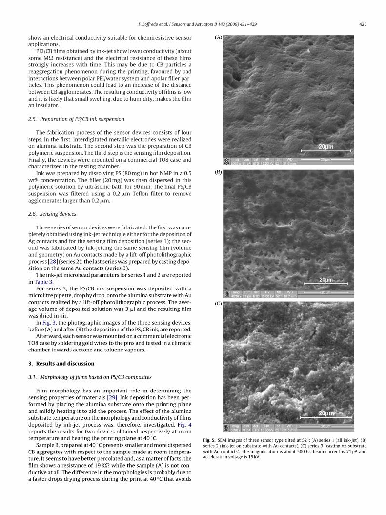
Fig. 5. SEM images of three sensor type tilted at 52◦: (A) series 1 (all ink-jet), (B)series 2 (ink-jet on substrate with Au contacts), (C) series 3 (casting on substrate
F. Loffredo et al. / Sensors an
how an electrical conductivity suitable for chemiresistive sensorpplications.
PEI/CB films obtained by ink-jet show lower conductivity (aboutome M� resistance) and the electrical resistance of these filmstrongly increases with time. This may be due to CB particles aeaggregation phenomenon during the printing, favoured by badnteractions between polar PEI/water system and apolar filler par-icles. This phenomenon could lead to an increase of the distanceetween CB agglomerates. The resulting conductivity of films is lownd it is likely that small swelling, due to humidity, makes the filmn insulator.
.5. Preparation of PS/CB ink suspension
The fabrication process of the sensor devices consists of fourteps. In the first, interdigitated metallic electrodes were realizedn alumina substrate. The second step was the preparation of CBolymeric suspension. The third step is the sensing film deposition.inally, the devices were mounted on a commercial TO8 case andharacterized in the testing chamber.
Ink was prepared by dissolving PS (80 mg) in hot NMP in a 0.5t% concentration. The filler (20 mg) was then dispersed in thisolymeric solution by ultrasonic bath for 90 min. The final PS/CBuspension was filtered using a 0.2 �m Teflon filter to removegglomerates larger than 0.2 �m.
.6. Sensing devices
Three series of sensor devices were fabricated: the first was com-letely obtained using ink-jet technique either for the deposition ofg contacts and for the sensing film deposition (series 1); the sec-nd was fabricated by ink-jetting the same sensing film (volumend geometry) on Au contacts made by a lift-off photolithographicrocess [28] (series 2); the last series was prepared by casting depo-ition on the same Au contacts (series 3).
The ink-jet microhead parameters for series 1 and 2 are reportedn Table 3.
For series 3, the PS/CB ink suspension was deposited with aicrolitre pipette, drop by drop, onto the alumina substrate with Au
ontacts realized by a lift-off photolithographic process. The aver-ge volume of deposited solution was 3 �l and the resulting filmas dried in air.
In Fig. 3, the photographic images of the three sensing devices,efore (A) and after (B) the deposition of the PS/CB ink, are reported.
Afterward, each sensor was mounted on a commercial electronicO8 case by soldering gold wires to the pins and tested in a climatichamber towards acetone and toluene vapours.
. Results and discussion
.1. Morphology of films based on PS/CB composites
Film morphology has an important role in determining theensing properties of materials [29]. Ink deposition has been per-ormed by placing the alumina substrate onto the printing planend mildly heating it to aid the process. The effect of the aluminaubstrate temperature on the morphology and conductivity of filmseposited by ink-jet process was, therefore, investigated. Fig. 4eports the results for two devices obtained respectively at roomemperature and heating the printing plane at 40 ◦C.
Sample B, prepared at 40 ◦C presents smaller and more dispersed
B aggregates with respect to the sample made at room tempera-ure. It seems to have better percolated and, as a matter of facts, thelm shows a resistance of 19 K� while the sample (A) is not con-uctive at all. The difference in the morphologies is probably due tofaster drops drying process during the print at 40 ◦C that avoidswith Au contacts). The magnification is about 5000×, beam current is 71 pA andacceleration voltage is 15 kV.

426 F. Loffredo et al. / Sensors and Actuators B 143 (2009) 421–429
on su
toh
doc1prsD
tPai(6
3
ts
euh
F
recovers to the baseline value. It is interesting to note that ink-jetfilms (series 1 and 2) recover completely after each measuring step
Fig. 6. FIB cut images of (A) a series 3 sample (casting sensing film
he riaggregation of CB particles. Therefore, all sensor devices basedn PS/CB/NMP films deposited by ink-jet were then manufactured,eating the printing plane at 40 ◦C.
The morphology of films obtained by ink-jet printing is veryifferent from those deposited by casting. Surface photographsbtained by SEM show that both the series 1 and 2 have a moreompact structure at the micrometer scale, as shown in Fig. 5. Series, in particular, appears to have a smooth surface and a denselyacked structure. In the casting films, the SEM image reveals augged surface composed of grains of about 300 nm in size, dimen-ion comparable with the CB mean particle size as measured byLS.
PS/CB composites were sectioned using the FIB equipment andheir thickness was evaluated. In Fig. 6A and B the FIB sections ofS/CB films deposited respectively by casting and by ink-jet ontolumina are shown. Nanocomposites thickness obtained by cast-ng is about 1.10 �m with a CB particles diameter of about 300 nmFig. 6A) while film PS/CB ink-jetted have a thickness of about00 nm (Fig. 6B).
.2. Electrical characterization of PS/CB sensor devices
In Fig. 7 the I/V characteristics in air at room temperature ofhe three series of devices are reported. The I/V plots are linear,
uggesting an ohmic behaviour for all the PS/CB sensors.The electrical resistance of series 1 (“all ink-jet” sample) is, how-ver, higher than that recorded for series 2 and 3. This was quitenexpected, since for both series 1 and 2, processing parametersad been tuned to obtain devices with impedance similar to series
ig. 7. Current (I)–Voltage (V) characteristics of series 1, 2 and 3, respectively.
bstrate with Au contacts) and (B) a series 1 sample (“all ink-jet”).
3. This difference has, therefore, to be related to either the differ-ent metal used for the electrodes and to the different electrodesdeposition technique.
Device resistances at different time of aging were then mea-sured. All devices exhibited a stable behaviour for the whole 60days observation time as it is apparent for data reported in Fig. 8.
3.3. Device responses to acetone and toluene vapours
Sensor devices have been tested in controlled atmosphere tomeasure the electrical responses to different acetone and tolueneconcentrations. Fig. 9 shows the normalized cycle curves for ace-tone concentrations from 600 ppm to 5000 ppm. All ink-jet-printedsensor devices have the dynamic electric responses to acetone typ-ical of PS/CB based sensors (see Fig. 9, where series 1, 2 and 3 arecompared). The device responses to the acetone have been deter-mined by the current intensity change defined as (I − I0)/I0 whereI0 is the sensor baseline current intensity and I is the sensor currentintensity upon its exposure to solvent vapours.
The current decreases when the device is exposed to acetonevapours up to an equilibrium value which is function of the vapourconcentration. When the flow of acetone is stopped the current
to their baseline levels after the VOC exposure is removed, differ-ently from what observed for the films obtained by casting (series
Fig. 8. The variation of the electrical resistances for the three devices observed inabout 60 days.

F. Loffredo et al. / Sensors and Actuators B 143 (2009) 421–429 427
Fs
3if
swfdcrsc
dttriftc
iw
rra
bl
a
Fig. 10. Responses at different concentrations of acetone for the sensor devices.
TT
Sp
ig. 9. Normalized dynamic responses at different concentrations of acetone for theensor devices (series 1 and 2 ink-jet, series 3 casting).
). The effect could be probably ascribed to lower thickness of thenk-jetted films, that could also explain the best relative responseor series 3 devices at the higher concentrations.
The sensitive performances of series 1 and 2 devices are quiteimilar except for the response time at the lower concentrationshich is smaller for series 2. This may be due to the different sur-
ace morphology caused by the different metal contacts. Series 2evices have a lower relative response and a faster response timeompared to the sensor obtained by casting (series 3). The minoreactive volume in series 2 together with its electrical resistanceimilar to series 3 devices suggest that polymer adhesion on Auontacts could be improved using ink-jet printing technique.
Such considerations are summarized in Table 4 where the mainevice parameters measured in the controlled environment of ace-one vapours are reported. The noise is given by fluctuations aroundhe measured resistance. Sensitivity is the slope of the electricalesponse at the different concentrations. The minimum detections the minimum analyte concentration that the sensor can detectrom the noise starting from the baseline. The response time ishe time interval between 10% and 90% of the response at a givenoncentration.
The quantitative responses obtained with sensors prepared bynk-jet processing (series 1 and 2) have been compared, in Fig. 10,
ith those of the series 3.All sensors series exhibit linear responses in the investigated
ange of concentrations. The series two sensors have higheresponse at 600 ppm compared to other sensors while at 1200 ppmnd 2400 ppm its response is similar to series 3 devices.
The improved behaviour of series two sensors is also confirmedy the measurements with toluene that can be injected at even
ower concentrations.In summary, the electrical test in controlled environment under
cetone exposure shows that:
Devices with ink-jetted polymeric film on ink-jetted silver trans-ducer (series 1) have the worst performances and this can beassigned to the transducer quality.
able 4he main device parameters measured in the controlled acetone environment.
Resistance (k�) Noise (�) Sensitivity (� ppm−1) Sensitiv
Series 1 90 50 0.29 0.019Series 2 20 50 0.082 2.4Series 3 18 10 0.014 2.7
eries 1 refers to devices with polymeric films deposited with ink-jet technique on ink-jehotolitographed gold transducer. Series 3 refers to devices with polymeric films deposita The minimum detection is the minimum analyte concentration that the sensor can d
Fig. 11. Sensitivity of the three series samples to toluene vapours.
Devices with ink-jetted polymeric film on photolitographedtranducer (series 2) have the best performance at the lower(<1000 ppm) concentration. This can be due to an improved finestsurface/volume ratio of the polymer film with respect to the castfilm and to a better polymer/gold electrode contact.Devices with polymeric film casted on Au photolitographed tran-ducer (serie3) have its best performance at high concentration(>1000 ppm) but slow kinetic thanks to its high volume sensinglayer.
The series 3 sensor devices have been investigated in a rangeof toluene concentrations from 60 ppm to 500 ppm. Fig. 11 showstoluene sensitivity measurements of all the tested devices. Polymernanocomposite have a polar affinity to toluene greater with respectto acetone so higher response is shown by all the devices.
The reproducibility of these sensors have been also evaluated.
The sensors have been tested several times in a two months timerange. Results are very encouraging since a relative data variationof most a 5% was measured in the whole time period.ity (%10−4 ppm−1) Min detection (ppma) Response time (0–90% min)
100 2030 470 20
tted silver transducer. Series 2 refers to devices with polymeric films ink-jetted oned by casting technique on photolitographed gold transducer.istinguish from the noise.

4 d Actu
3
cb
ddiNueittssto
A
d
R
[
[
[
[
[
[
[
[
[
[
[
[
[
[
[
[
[
[
[
[
28 F. Loffredo et al. / Sensors an
.4. Conclusions
The work described in this paper suggests that ink-jet printingan be effectively used to produce sensors based on polymer/carbonlack composites.
We studied and optimized ink-jet parameters (amplitude anduration of jetting impulse, substrate velocity) to obtain sensorevices based on PS/CB surfaces. The manufacture of a VOC chem-
cal sensor completely by ink-jet processing has been shown.amely, the electrodes and the sensing films were fabricatedsing the same tool. This is a first step to obtain an all printedlectronic circuit, for sensing applications. The performances ofnk-jet-printed sensors at low concentrations are comparable tohose of the casting sensor devices. By comparing the responsesowards acetone and toluene vapours, it is clearly evident that theensor response is affected by the ink deposition method. ink-jettedensitive films show good sensitivity especially at low concentra-ion. ink-jetted silver transducers need further investigation andptimization.
cknowledgement
The support by the TRIPODE project financed by the Ministeroell’Università e della Ricerca (MUR) is gratefully acknowledged.
eferences
[1] R.F. Service, Science 304 (2004) 675.[2] P. Calvert, Ink-jet printing for materials and devices, Chem. Mater. 13 (2001)
3299–3305.[3] B.J. de Gans, P.C. Duineveld, U.S. Schubert, Ink-jet ptrinting of polymers: state
of the art and future developments, Adv. Mater. 16 (2004) 203–213.[4] E. Tekin, B.J. de Gans, U.S. Schubert, Ink-jet printing of polymers—from single
dots to thin film libraries, J. Mater. Chem. 14 (2004) 627–2632.[5] E. Segal, R. Tchoudakov, M. Narkis, A. Siegmann, Y. Wei, Polystyrene/polyaniline
nanoblends for sensing of aliphatic alcohols, Sen. Actuators B 104 (2005)140–150.
[6] C. Moldovan, L. Hinescu, M. Hinescu, R. Iosub, M. Nisulescu, B. Firtat, M. Mod-reanu, D. Dascalu, V. Voicu, C. Tarabasanu, Silicon micromachined sensor forgas detection, Mater. Sci. Eng. B 101 (2003) 227–231.
[7] A. Fujii, H. Mizukami, Y. Hashimoto, T. Umeda, Y. Nishihara, M. Ozaki, K. Yoshino,Highly efficient photovoltaic cells composed of interpenetrating conductingpolymer/C60 heterojunction, Synth. Met. 152 (2005) 121–124.
[8] Y. Zhang, Y. Guan, J. Liu, J. Xu, W. Cao, Fabrication of covalently attachedconducting multilayer self-assembly film of polyaniline by in situ couplingreaction, Synth. Met. 128 (2002) 305–309.
[9] S. Chatzandroulis, N. Andreadis, D. Goustouridis, L. Quercia, I. Raptis, K. Beltsios,Composite chemical sensors based on carbon-filled patterned negative resists,Jpn. J. Appl. Phys. B 46 (2007) 6423–6428.
10] R. Parashkov, E. Becker, T. Riedl, H.H. Johannes, W. Kowalsky, Large area elec-tronics using printing methods, Proc. IEEE 93 (2005) 1321–1329.
11] A. Bietsch, J. Zhang, M. Hegner, H.P. Lang, C. Gerber, Rapid functionalizationof cantilever array sensors by ink-jet printing, Nanotechnology 15 (2004)873–880.
12] S. Wenfeng, Y. Zhaoa, C. Zhang, The preparation of ZnO based gas-sensing thinfilms by ink-jet printing method, Thin Solid Films 483 (2005) 382–387.
13] D.L. McCorkle, R.J. Warmack, S.V. Patel, T. Mlsna, S.R. Hunter, T.L. Ferrell, Ethanolvapor detection in aqueous environments using micro-capacitors and dielectricpolymers, Sens. Actuators B 107 (2005) 892–903.
14] J.C. Carter, R.M. Alvis, S.B. Browna, K.C. Langry, T.S. Wilson, M.T. McBride, M.L.Myrick, W. Royall Cox, M.E. Grove c, B.W. Colston, Fabricating optical fiber imag-ing sensors using ink-jet printing technology: a pH sensor proof-of-concept,Biosens. Bioelectron. 21 (2006) 1359–1364.
15] M.F. Mabrook, C. Pearson, M.C. Petty, Inkjet-printed polymer films for the detec-tion of organic vapours, IEEE Sens. J. 6 (2006) 1435–1444.
16] M.F. Mabrook, C. Pearson, M.C. Petty, Inkjet-printed polypyrrole thin films forvapour sensing, Sens. Actuators B 115 (2006) 547–551.
17] B. Li, S. Santhanam, L. Schultz, M. Jeffries EL, M.C. Iovu, G. Sauvè, J. Cooper,R. Zhang, J.C. Revelli, A.G. Kusne, J.L. Snyder, T. Kowalewski, L.E. Weiss, R.D.McCullough, G.K. Fedder, D.N. Lambeth, Ink-jet printed chemical sensor arraybased on polythiophene conductive polymers, Sens. Actuators B 123 (2007)651–660.
18] F. Loffredo, G. Burrasca, L. Quercia, D. Della Sala, Gas sensor devices obtainedby ink-jet printing of polyaniline suspensions, Macromol. Symp. 247 (2007)357–363.
19] K. Crowley, E. O’Malley, A. Morrin, M.R. Smyth, A.J. Killard, An aqueous ammoniasensor based on an inkjet-printed polyaniline nanoparticle-modified electrode,Analyst 133 (2008) 391–399.
ators B 143 (2009) 421–429
20] M.S. Freund, N.S. Lewis, A chemically diverse, conducting polymer-based elec-tronic nose, Proc. Natl. Acad. Sci. U.S.A. 92 (1995) 2652–2656.
21] L. Quercia, F. Loffredo, B. Alfano, V. La Ferrara, G. Di Francia, Fabrication andcharacterization of carbon nanoparticles for polymer based vapor sensors, Sens.Actuators B 100 (2004) 22–28.
22] B.J. Doleman, M.C. Lonergan, E.J. Severin, T.P. Vaid, N.S. Lewis, Quantitativestudy of the resolving power of arrays of carbon black-polymer compositesin various vapor-sensing tasks, Anal. Chem. 70 (1998) 4177.
23] M.E. Koscho, R.H. Grubbs, N.S. Lewis, Properties of vapor detector arraysformed through plasticization of carbon black-organic polymer composites,Anal. Chem. 74 (2002) 1307.
24] D.R. Lide (Ed.), Handbook of Chemistry and Physics, vol.12, 77th ed., CRC press,Boca Raton, 1996, 12–41 pp.
25] D. Kim, J. Moon, Highly conductive ink jet printed films of nanosilver particlesfor printable electronics, Electrochem. Solid-State Lett. 8 (2005) J30–J33.
26] A.L. Dearden, P.J. Smith, D.Y. Shin, N. Reis, B. Derby, P. O’Brien, A lowcuring temperature silver ink for use in ink-jet printing and subsequent pro-duction of conductive tracks, Macromol. Rapid Commun. 26 (2005) 315–318.
27] T.H.J. Van Osch, J. Perelaer, A.W.M. de Laat, U.S. Schubert, Ink-jet printing ofnarrow conductive tracks on untreated polymeric substrates, Adv. Mater. 20(2008) 343–345.
28] B. Philip, J.K. Abraham, A. Chandrasekhar, V.K. Varadan, Carbon nan-otube/PMMA composite thin films for gas-sensing applications, Smart Mater.Struct. 12 (2003) 935–939.
29] L. Quercia, F. Loffredo, G. Di Francia, Influence of filler dispersion on thin filmcomposites sensing properties, Sens. Actuators B 109 (2005) 153–158.
Biographies
Fausta Loffredo graduated with honors in chemistry at university of salerno (Italy)in 1998 and received her PhD in chemistry from the same university in February2002. Hers doctoral work focused on the synthesis and characterization of syndio-tactic homopolymer and copolymers of styrene that was able to form crystallineclathrate and nanoporous forms. The last ones were used as thermoplastic molecularsieves. In October 2001 she won a scholarship in field of macromolecular chemistryand she studied problems relative to use of multilayer films of physical recycledpolymers in alimentary applications. In May 2002 she began her activities at ENEA-Centro Ricerche in the area of polymeric sensors based on polymeric nanocomposite.In October 2004 she won a position as a researcher at ENEA-Centro Ricerche. Hercurrent research interest is the ink-jet printing of polymeric materials to use insensor and electronic applications.
Anna De Girolamo Del Mauro received the degree in chemistry from the universityof salerno, Italy (2001) and the PhD degree in chemistry from the same univer-sity (2004). She has been working at the ENEA research center in Portici (NA) sinceOctober 2006. Her research is focused on fabrication and characterization of poly-mer/conductive filler composites based chemical vapour sensors.
Gianbattista Burrasca graduated in Electronics Engineering–Telecommunicationssector at University of Ancona (Italy) in 2000 with a thesis on electromagneticdiffraction problems. In March 2001 he began activities in designing of photovoltaicsystems and electronic circuits for photovoltaic applications, employee in a privatecompany. In October 2004 he began at ENEA-Centro Ricerche, studies and activitiesrelated to ink-jet techniques for functional material’s deposition and embossingtechnique for polymeric material’s manipulation, finalized to development of newproduction techniques for electronic devices.
Vera La Ferrara was born in Lanciano, Chieti, Italy, in 1967. She graduated in physicsfrom the University “Federico II” of Naples, Italy, in 1994. Since 2000 she is researcherat the Department of Physical Technologies and New Materials—section ‘Nanomate-rials and Devices Technologies’ in ENEA Research Center in Portici. Her main researchinterests are chemical and electrochemical techniques for porous silicon and nano-structured materials fabrication. She works on fabrication and characterization ofsensors based on nanowires or on commercial carbon nanotubes, manufacturingand optical characterization of polymeric templates and devices fabrication for drugdelivery. Currently she works on nanomachining through Focused Ion Beam (FIB).Dr. La Ferrara has coauthored over several publications published on internationaljournals and conference proceedings. She is currently referee of international jour-nals. She is also tutor of several thesis and PhD assigned by the University ‘FedericoII’ of Naples, Italy.
Luigi Quercia graduated with honors in physics at university of Naples in 1989and worked for three years between Trento and Naples setting up a laboratory forhigh-resolution spectroscopy techniques of metastable oxygen atoms in a cooledsupersonic molecular beam. In March 1992 won a permanent position as researcherat ENEA-Centro Ricerche where has been working for the next five years on photo-voltaic thin film cells and modules participating to many European projects. Since
1996 his interests focused on porous silicon, nano-structured materials and poly-mers used as sensitive elements for room temperature solid-state gas sensors. Heis author of about 30 publications on international journals and more than 60 com-munications to national and international conferences.Ettore Massera was born in Naples, Italy, in 1969. He received his degree in physicsfrom the “Federico II” University of Naples in May 1997. He has been working at the

d Actu
ErMs
Gpfimwcdt
“La Sapienza”–Rome (1983). He worked in Eni ricerche (ENI group) for industrial
F. Loffredo et al. / Sensors an
NEA research center in Portici (NA) from June 2003. At present he is in charge ofesearch activity on gas sensor devices based on nano-structured materials. Dr. E.assera previously worked on the study of thermal and optical properties of porous
ilicon at the physics Department in Naples.
irolamo Di Francia was born in Naples, Italy, in 1958. He received his degree inhysics from the University of Naples. In 1985 he started his research activity in the
eld of fabrication and characterization of semiconductor solar cells (c-Si, GaAs), for-erly in Ansaldo (Genova), and then in the ENEA research center of Rome, where heas appointed full time researcher in 1988. From 1991 he joined the ENEA researchenter of Naples where, starting from 1992, he investigated Porous Silicon basedevices. In 1996 he established there the Gas Sensor Laboratory mainly devotedo the fabrication and characterization of devices based on nanomaterials and on
ators B 143 (2009) 421–429 429
polymers nanocomposites. During his scientific activity Dr. Girolamo Di Franciapublished more than 60 scientific papers on international reviews and presentednumerous communications in national and international congresses.
Dario Della Sala is the “Head of Section” in the Department for Physical Technolo-gies and New Materials of ENEA. He has a degree in Physics from the University
research on solar cells and thin film transistor processing. At ENEA from 1990, hehas worked in the development of thin film technologies applied to photovoltaicsolar cells and to polymer electronics, OLED display and gas sensors. In this periodhe has leaded several teams and projects in the mentioned fields, and has been theauthor of 60 scientific papers and five patents.