
Industrial System Engineering for Drones
268
TECHNOLOGY IN ACTION™ Industrial System Engineering for Drones A Guide with Best Practices for Designing — Neeraj Kumar Singh Porselvan Muthukrishnan Satyanarayana Sanpini
-
Upload
khangminh22 -
Category
Documents
-
view
0 -
download
0
Transcript of Industrial System Engineering for Drones

T E C H N O L O G Y I N A C T I O N ™
Industrial System Engineering for Drones
A Guide with Best Practices for Designing—Neeraj Kumar SinghPorselvan MuthukrishnanSatyanarayana Sanpini

Industrial System Engineering for
DronesA Guide with Best Practices
for Designing
Neeraj Kumar SinghPorselvan MuthukrishnanSatyanarayana Sanpini

Industrial System Engineering for Drones: A Guide with Best Practices for
Designing
ISBN-13 (pbk): 978-1-4842-3533-1 ISBN-13 (electronic): 978-1-4842-3534-8https://doi.org/10.1007/978-1-4842-3534-8
Copyright © 2019 by Neeraj Kumar Singh, Porselvan Muthukrishnan, Satyanarayana Sanpini
This work is subject to copyright. All rights are reserved by the Publisher, whether the whole or part of the material is concerned, specifically the rights of translation, reprinting, reuse of illustrations, recitation, broadcasting, reproduction on microfilms or in any other physical way, and transmission or information storage and retrieval, electronic adaptation, computer software, or by similar or dissimilar methodology now known or hereafter developed.
Trademarked names, logos, and images may appear in this book. Rather than use a trademark symbol with every occurrence of a trademarked name, logo, or image we use the names, logos, and images only in an editorial fashion and to the benefit of the trademark owner, with no intention of infringement of the trademark.
The use in this publication of trade names, trademarks, service marks, and similar terms, even if they are not identified as such, is not to be taken as an expression of opinion as to whether or not they are subject to proprietary rights.
While the advice and information in this book are believed to be true and accurate at the date of publication, neither the authors nor the editors nor the publisher can accept any legal responsibility for any errors or omissions that may be made. The publisher makes no warranty, express or implied, with respect to the material contained herein.
Managing Director, Apress Media LLC: Welmoed SpahrAcquisitions Editor: Natalie PaoDevelopment Editor: James MarkhamCoordinating Editor: Jessica Vakili
Cover image designed by Freepik (www.freepik.com)
Distributed to the book trade worldwide by Springer Science+Business Media New York, 233 Spring Street, 6th Floor, New York, NY 10013. Phone 1-800-SPRINGER, fax (201) 348-4505, e-mail [email protected], or visit www.springeronline.com. Apress Media, LLC is a California LLC and the sole member (owner) is Springer Science + Business Media Finance Inc (SSBM Finance Inc). SSBM Finance Inc is a Delaware corporation.
For information on translations, please e-mail [email protected], or visit www.apress.com/rights-permissions.
Apress titles may be purchased in bulk for academic, corporate, or promotional use. eBook versions and licenses are also available for most titles. For more information, reference our Print and eBook Bulk Sales web page at www.apress.com/bulk-sales.
Any source code or other supplementary material referenced by the author in this book is available to readers on GitHub via the book's product page, located at www.apress.com/978-1-4842-3533-1. For more detailed information, please visit www.apress.com/source-code.
Printed on acid-free paper
Neeraj Kumar SinghBangalore, India
Porselvan MuthukrishnanBangalore, India
Satyanarayana SanpiniBangalore, India

Dedicated to my sons, Anant and Atulya, for filling my life with joy and inspiration
—Neeraj
Dedicated to my teachers and mentors
—Satya
Dedicated to my teachers and mentors
—Porselvan

v
About the Authors ������������������������������������������������������������������������������xiii
Acknowledgments ������������������������������������������������������������������������������xv
Table of Contents
Chapter 1: Introduction�������������������������������������������������������������������������1
What Is a Drone? ���������������������������������������������������������������������������������������������������2
Military ������������������������������������������������������������������������������������������������������������2
Industrial ���������������������������������������������������������������������������������������������������������3
Commercial �����������������������������������������������������������������������������������������������������3
Parts of a Drone System ���������������������������������������������������������������������������������������4
Hardware ���������������������������������������������������������������������������������������������������������4
Software ��������������������������������������������������������������������������������������������������������10
Mechanical ����������������������������������������������������������������������������������������������������12
Ground-Based Controllers and Accessories ��������������������������������������������������14
Summary�������������������������������������������������������������������������������������������������������������15
Chapter 2: Drone System Design Flow �����������������������������������������������17
System Design ����������������������������������������������������������������������������������������������������17
Requirement Specification ����������������������������������������������������������������������������18
Architecture ���������������������������������������������������������������������������������������������������19
Implementation ���������������������������������������������������������������������������������������������23
Specifications for Our Drone, “Crop Squad” ��������������������������������������������������23

vi
Mechanical Design ����������������������������������������������������������������������������������������������24
Definition �������������������������������������������������������������������������������������������������������26
Purpose ���������������������������������������������������������������������������������������������������������27
Requirements ������������������������������������������������������������������������������������������������28
Dependencies ������������������������������������������������������������������������������������������������32
Hardware Design ������������������������������������������������������������������������������������������������32
Hardware Requirements ��������������������������������������������������������������������������������33
Electrical Ingredients Selection ���������������������������������������������������������������������35
PCBA Design ��������������������������������������������������������������������������������������������������37
Floor Plan ������������������������������������������������������������������������������������������������������43
Power Architecture ����������������������������������������������������������������������������������������44
Software Architecture �����������������������������������������������������������������������������������������58
Logistics and Operations Management ���������������������������������������������������������������60
Board and System Assembly �������������������������������������������������������������������������61
Summary�������������������������������������������������������������������������������������������������������������62
Chapter 3: Key Ingredients and Selection Considerations ������������������63
System on a Chip ������������������������������������������������������������������������������������������������64
Categories �����������������������������������������������������������������������������������������������������65
Key Considerations ����������������������������������������������������������������������������������������66
Solutions ��������������������������������������������������������������������������������������������������������66
Memory ���������������������������������������������������������������������������������������������������������������67
Categories �����������������������������������������������������������������������������������������������������67
Key Considerations ����������������������������������������������������������������������������������������70
Solutions ��������������������������������������������������������������������������������������������������������71
Storage ����������������������������������������������������������������������������������������������������������������73
Categories �����������������������������������������������������������������������������������������������������73
Key Considerations ����������������������������������������������������������������������������������������81
Solutions ��������������������������������������������������������������������������������������������������������82
Table of ConTenTsTable of ConTenTs

vii
Communication Module ��������������������������������������������������������������������������������������83
Categories �����������������������������������������������������������������������������������������������������84
Key Considerations ����������������������������������������������������������������������������������������86
Solution ���������������������������������������������������������������������������������������������������������87
Camera ����������������������������������������������������������������������������������������������������������������88
Categories �����������������������������������������������������������������������������������������������������88
Key Considerations ����������������������������������������������������������������������������������������90
Solutions ��������������������������������������������������������������������������������������������������������90
Display ����������������������������������������������������������������������������������������������������������������92
Categories �����������������������������������������������������������������������������������������������������92
Key Considerations ����������������������������������������������������������������������������������������93
Flight Controllers �������������������������������������������������������������������������������������������������94
Categories �����������������������������������������������������������������������������������������������������94
Key Considerations ����������������������������������������������������������������������������������������95
Solutions ��������������������������������������������������������������������������������������������������������95
Battery ����������������������������������������������������������������������������������������������������������������95
Categories �����������������������������������������������������������������������������������������������������96
Key Considerations ����������������������������������������������������������������������������������������97
Solutions ��������������������������������������������������������������������������������������������������������98
Thermal Solution �������������������������������������������������������������������������������������������������99
Categories �����������������������������������������������������������������������������������������������������99
Key Considerations ��������������������������������������������������������������������������������������100
Solutions ������������������������������������������������������������������������������������������������������101
Interconnects ����������������������������������������������������������������������������������������������������101
Categories ���������������������������������������������������������������������������������������������������102
Key Considerations ��������������������������������������������������������������������������������������105
Solutions ������������������������������������������������������������������������������������������������������106
Table of ConTenTsTable of ConTenTs

viii
Mechanicals ������������������������������������������������������������������������������������������������������106
Categories ���������������������������������������������������������������������������������������������������106
Key Considerations ��������������������������������������������������������������������������������������107
Solutions ������������������������������������������������������������������������������������������������������108
Summary�����������������������������������������������������������������������������������������������������������108
Chapter 4: Drone Hardware Development ����������������������������������������111
PCB Library Development ���������������������������������������������������������������������������������112
Symbol Creation ������������������������������������������������������������������������������������������112
Schematics Design �������������������������������������������������������������������������������������������116
Schematics Capture ������������������������������������������������������������������������������������117
Design Rules Checking ��������������������������������������������������������������������������������118
Generating a Netlist �������������������������������������������������������������������������������������119
Bill of Materials �������������������������������������������������������������������������������������������������119
Symbol Attributes ����������������������������������������������������������������������������������������121
BOM Generation �������������������������������������������������������������������������������������������122
Material Readiness ��������������������������������������������������������������������������������������123
Layout Design ���������������������������������������������������������������������������������������������������123
Board Outline �����������������������������������������������������������������������������������������������124
Layer Stack-Up ��������������������������������������������������������������������������������������������124
Electrical Constraints�����������������������������������������������������������������������������������125
Mechanical Constraints �������������������������������������������������������������������������������130
Netlist ����������������������������������������������������������������������������������������������������������134
Summary �����������������������������������������������������������������������������������������������������138
Table of ConTenTsTable of ConTenTs

ix
Chapter 5: System Assembly, Bring-Up and Validation ��������������������139
PCB Fabrication Process �����������������������������������������������������������������������������������140
Fabrication Steps�����������������������������������������������������������������������������������������140
PCB Assembly Process��������������������������������������������������������������������������������������142
Surface Mount Assembly Process ���������������������������������������������������������������144
Through Hole Assembly Process �����������������������������������������������������������������148
Final Inspection and Functional Test �����������������������������������������������������������149
Post Process ������������������������������������������������������������������������������������������������149
Board Power-On ������������������������������������������������������������������������������������������������150
Basic Inspection ������������������������������������������������������������������������������������������151
Short-Circuit Checks �����������������������������������������������������������������������������������151
Power Check������������������������������������������������������������������������������������������������152
Sequencing and Reset Check ����������������������������������������������������������������������153
Board-Level Testing ������������������������������������������������������������������������������������������154
BIOS Flash Programming �����������������������������������������������������������������������������154
OS and Application Installation ��������������������������������������������������������������������155
Functionality Check �������������������������������������������������������������������������������������155
Design Validation Testing ����������������������������������������������������������������������������������156
Power Validation ������������������������������������������������������������������������������������������157
Electrical Validation �������������������������������������������������������������������������������������161
Drone Assembly ������������������������������������������������������������������������������������������������163
Drone System Validation Testing �����������������������������������������������������������������163
System Pilot Build ���������������������������������������������������������������������������������������164
Summary�����������������������������������������������������������������������������������������������������������165
Table of ConTenTsTable of ConTenTs

x
Chapter 6: Software Development ����������������������������������������������������167
Software Development and Deployment �����������������������������������������������������������167
Software Development Life Cycle ����������������������������������������������������������������168
Software Stack ��������������������������������������������������������������������������������������������173
Key Considerations of Drone Software Design ��������������������������������������������180
System Software Integration and Bring-Up �������������������������������������������������202
System Bring-Up �����������������������������������������������������������������������������������������202
Verification, Validation, and Maintenance ����������������������������������������������������208
Conclusion ���������������������������������������������������������������������������������������������������213
Chapter 7: Drone Product Certification ���������������������������������������������215
Regulatory Certification ������������������������������������������������������������������������������������216
Safety ����������������������������������������������������������������������������������������������������������216
Emission ������������������������������������������������������������������������������������������������������219
Immunity �����������������������������������������������������������������������������������������������������220
Environmental Certification �������������������������������������������������������������������������������222
Temperature ������������������������������������������������������������������������������������������������223
Humidity ������������������������������������������������������������������������������������������������������223
Altitude ��������������������������������������������������������������������������������������������������������224
Drop, Shock, and Vibration ��������������������������������������������������������������������������224
Reliability �����������������������������������������������������������������������������������������������������225
Service and Support �����������������������������������������������������������������������������������������225
Pilot Distribution ������������������������������������������������������������������������������������������225
Device Software Upgrade ����������������������������������������������������������������������������226
Technical Service ����������������������������������������������������������������������������������������226
Product Ecology ������������������������������������������������������������������������������������������������226
Prohibited Substances ���������������������������������������������������������������������������������226
ROHS �����������������������������������������������������������������������������������������������������������228
Table of ConTenTsTable of ConTenTs

xi
EU REACH ����������������������������������������������������������������������������������������������������229
California Proposition 65 �����������������������������������������������������������������������������229
WEEE �����������������������������������������������������������������������������������������������������������230
ISO ���������������������������������������������������������������������������������������������������������������230
Product Certification Centers ����������������������������������������������������������������������������230
Device Costing ��������������������������������������������������������������������������������������������������230
Production Cost �������������������������������������������������������������������������������������������231
Accessories Cost �����������������������������������������������������������������������������������������231
Drone Regulations ���������������������������������������������������������������������������������������������231
Regulations ��������������������������������������������������������������������������������������������������232
Drone Registration ���������������������������������������������������������������������������������������232
Summary�����������������������������������������������������������������������������������������������������������232
Appendix I: Schematics Basics ��������������������������������������������������������233
Reading Schematics ����������������������������������������������������������������������������������������� 236
Layout Basics ���������������������������������������������������������������������������������������������������� 237
Electronic System Design Communication interfaces �������������������������������������� 238
High Speed Interfaces ��������������������������������������������������������������������������������������� 241
Pulse-shaping ���������������������������������������������������������������������������������������������� 243
Reliability/durability ������������������������������������������������������������������������������������� 245
Low Speed Communication Interfaces ������������������������������������������������������������� 245
Appendix II: References ��������������������������������������������������������������������247
Epilogue ��������������������������������������������������������������������������������������������249
Index �������������������������������������������������������������������������������������������������251
Table of ConTenTsTable of ConTenTs

xiii
About the Authors
Neeraj Kumar Singh has been a Platform Architect for Intel Client
platforms for more than 12 years. His areas of expertise are hardware/
software co-design, SoC system/platform architecture, and system
software design and development. Neeraj is the author of System on Chip
Interfaces for Low Power Design and The Impact of Loop Unrolling on
Controller Delay in High Level Synthesis.
Porselvan Muthukrishnan has been a Hardware/System Design
Engineer for Intel IOT platforms for over 10 years. His area of expertise is
hardware/system design. Porselvan is currently working on system designs
for connected home, connected cars, and other IoT devices.
Satyanarayana Sanpini has been working in the fields of low-power
embedded systems architecture, SoC definition, architecture, and design
for the past 17+ years. He has contributed in various technical positions
at start-ups Ittiam, Beceem Communications, and MNCs Broadcom,
and also Qualcomm and Intel. He is currently based out of Bangalore,
India and works at Intel India Center. Satya obtained his M.Tech degree
in Electronics Design from Indian Institute of Science (IISc), Bangalore,
India. Apart from a passion for technology, Satya likes to spend time with
his young kids and explore nature’s grandeur through travel and trek.

xv
Acknowledgements
We would like to express gratitude to the people who helped us through
this book; some of them directly and many others indirectly.
It's impossible to not risk missing someone, but we will attempt
anyway.
First and foremost, we would like to acknowledge Vinay K C and
Balachandar Santhanam for their guidance and time in review. Vinay
and Bala, your detailed review helped the book significantly in terms of
structure, content, and quality; thank you very much!!
We would like to thank Intel management for the support and
encouragement.
Above all, we thank our families and friends for their understanding,
support, and being continuous source of encouragement.
1© Neeraj Kumar Singh, Porselvan Muthukrishnan, Satyanarayana Sanpini 2019N. K. Singh et al., Industrial System Engineering for Drones, https://doi.org/10.1007/978-1-4842-3534-8_1
CHAPTER 1
IntroductionSystem design is a discipline of creating a system/product, starting from
requirements to the final deployment in the field. It is a very vast subject
and encompasses multiple cross-functional domains such as market
research, planning, product definition, hardware design, software design,
industrial design, validation, certification, etc. It is very difficult to cover all
of these aspects in detail in a single book. This may be why few references
cover the system design in detail. This book is an attempt to provide a brief
introduction to the system design discipline.
As anyone can understand, a vast variety of systems are possible in the
real world. The focus of this book is a typical electromechanical system
design, with emphasis on electrical hardware system design concepts. You
will be taken through the processes and methodologies comprehensively
using the fairly complex electromechanical system of a drone as an
example. While this book primarily focuses on the electrical part of the
system design, other critical disciplines like mechanicals and software
are covered at a high level to give a complete perspective of the system
design. To give you a feel of designing a system from scratch yourself, at
many places the content is presented from a first-person perspective. By
end of the book, you will get a glimpse of how multiple subsystems are
developed or chosen carefully (components are either “make” or “buy”)
to get a flawless system (through the drone example). The focus areas
vary dynamically, but “make” components are emphasized more than
“buy” components. Hardware is always a make item for most of the system
design, so that’s why it’s covered in so much detail.

2
The organization of the book is as follows. In Chapter 1, we start with
brief description of the drone system and its critical components. In
Chapter 2, the typical system design flow details are presented. Chapter 3
delves into the drone system’s key ingredients and selection procedure.
In Chapter 4, the electronic hardware development process is covered
in detail. Chapter 5 covers typical procedures and checks followed as
part of a system bring-up. In Chapter 6, the software processes and real-
time software that go into drone-like systems are discussed. Chapter 7
concludes the book with coverage of the final certification processes a
system needs to go through before deployment. Two appendixes provide
additional basics and references.
What Is a Drone?An unmanned aerial vehicle (UAV), commonly known as a drone, is
an aircraft without a human pilot onboard. UAVs are a component of
an unmanned aircraft system, which includes a UAV, a ground-based
controller, and a system of communications between the two. The flight of
UAVs may operate with various degrees of autonomy, either under remote
control by a human operator or autonomously by onboard computers.
Drones are classified into different categories based on the
applications. Applications are broad, and from the design perspective,
generally fall under three major groups: military, industrial (enterprise),
and commercial.
MilitaryDrones in military applications are used for anti-aircraft target practice,
intelligence gathering and, more controversially, as weapons platforms.
Chapter 1 IntroduCtIon

3
IndustrialThe integration of drones and IoT (Internet of Things) technology has
created numerous industrial and enterprise use cases: drones working
with on-ground IOT sensor networks can help agricultural companies
monitor land and crops, energy companies survey power lines and
operational equipment, and insurance companies monitor properties for
claims and/or policies.
CommercialThe commercial field is a growing development, where the largest,
strongest, fastest, and most capable drones on the market are targeted
toward the professional community. They are the types of machines
that the movie industry puts to work and that commercial agencies use
to inspect infrastructure. Some impressive self-piloted drones survey
individual farmer’s fields. Commercial drones are the smaller consumer
products that make up just a tiny portion of the overall drone market.
Figure 1-1 shows the form factor of a commercial drone.
Figure 1-1. Commercial drone
Chapter 1 IntroduCtIon

4
Parts of a Drone SystemFrom an engineer’s view, the key parts of a drone system are the hardware,
software, and mechanical elements; and a perfect balance between the
three provides a flawless system design.
HardwareHardware is the electrical part of the drone system, which is eventually
a PCBA (printed circuit board assembly). Hardware is a multilayer
PCB that accommodates the SOC (system on a chip) and different
components of the subsystems interconnected through copper traces (part
of the PCB) or physical wires. Figure 1-2 shows the PCBA assembled with
SOC and subsystems on the top side (primary side).
Figure 1-2. PCBA mounted with SOC and subsystems
Chapter 1 IntroduCtIon

5
The SOC
The SOC is a miniature computer on a chip of a present generation
systems, especially a drone system. It’s a semiconductor device and an
integrated circuit that usually integrates digital, analog, mixed signal, and
radio frequency devices on a single chip. SOCs are most commonly used in
mobile computing and embedded systems.
In general, there are three distinguishable types of SOCs: SOCs built
around a microcontroller, SOCs built around a microprocessor, and
specialized SOCs designed for specific applications that do not fit into the
above two categories.
SOC usually consume less power and have a lower cost than the
multichip systems they replace.
Note Intel Core, atom, and Quark processors are SoCs on a single package.
Figure 1-3 shows a typical SOC that integrate digital, analog, and
mixed signal devices on a single chip. The device at the center of the SOC
is the silicon, and some capacitors are distributed on the top side of the
SOC. The bottom side of the SOC shows pins (called as balls in a ball grid
array), which are soldered on to a PCB to establish the connection with
the subsystems through PCB traces. You’ll see more details on this in later
sections.
Chapter 1 IntroduCtIon

6
Subsystems
Subsystems or electrical subsystems are technologies required in a system
to fulfill the intended usage of the system.
Broadly speaking, subsystems fall into any one of the following
computer architecture parts: input, output, storage, and communication
devices.
Input
A touch panel, keyboard, mouse, microphone, camera, sensors, and
remote control are some examples of input devices of a system.
Figure 1-3. Top and bottom views of the SOC
Chapter 1 IntroduCtIon

7
Output
Displays, speakers, motors, fans, and LEDs are some examples of output
devices of a system.
Storage
Memory, flash, hard disk drive, optical drive, secure digital, and solid state
drive are some examples of the storage devices of a system.
Communication Devices
Wired LAN (local area network), wireless LAN, mobile networks (3G, 4G,
and LTE), GPS (Global Positioning System), and USB are some examples of
the communication devices of a systems.
All of the subsystems listed above may or may not be a part of a
particular drone design. The target application picks the right subsystems
to be part of the drone system design.
For example, if the intended application of a drone is surveillance, it
should be equipped with a high resolution camera and the SOC used in
the system should be capable of accepting and processing the high speed
data from that camera. The PCBA should be designed in such a way as to
interconnect the high speed data between SOC and the camera module
and then be capable of transmitting the live or recorded data via the
wireless communication modules.
Besides SOC, the camera module, wireless module (WiFi/3G/4G modules),
memory, internal storage, sensors, and flight controllers are the basic
required subsystems for a surveillance drone. Figure 1-4 is the transparent
view of the internal parts of the drone, highlighting a few high- level
subsystems, which are visible.
Chapter 1 IntroduCtIon

8
Subsystems play an important role in defining the specifications of the
product. (“Product” is the right term for a system when in production stage
and available in the market). An end user will see these subsystems as a
feature list when selecting a product. A typical drone will have the features
listed in Table 1-1.
Figure 1-4. Parts of a drone
Table 1-1. Basic Features of a Drone
Features Specifications
Camera pixels 2Mp, 720phd
Controller 2.4Ghz
Channels 4 channels
Gyroscope 6-axis control
distance Control by phone about 164ft/
Control by controller about 262ft
Battery for quadcopter 3.7V 900mah li-po battery
Chapter 1 IntroduCtIon

9
Table 1-2 lists the specifications covering additional internal features of
the drone system. It must again be noted that the specification here is for
an example drone and will vary from one drone system to another. As seen
earlier, some subsystems from the list may or may not be required for the
target application of the system.
Table 1-2. Detailed Features of a Drone System
Subsystems Features Specifications
netWorK technology GSM / CdMa / hSpa / eVdo / Lte
proCeSSInG Cpu Quad-core 2.34 Ghz
Gpu 6-core graphics
MeMorY Card slot no
Internal 32/128/256 GB, 2 GB raM
CaMera primary 12 Mp (f/1.8, 28mm, 1/3"), phase detection autofocus,
oIS, quad-Led dual-tone flash, check quality
Features Geo-tagging, simultaneous 4K video and 8Mp image
recording, touch focus, face/smile detection, hdr
(photo/panorama)
Video 2160p@30fps, 1080p@30/60/120fps, 720p@240fps,
check quality
Secondary 7 Mp (f/2.2, 32mm), 1080p@30fps, 720p@240fps,
face detection, hdr, panorama
audIo alert types Vibration
Loudspeaker Yes, with stereo speakers
3.5mm jack no
(continued)
Chapter 1 IntroduCtIon

10
SoftwareThere are three or maybe four categories of software that we’d use on the
drone system:
1. Firmware components: Many of the HW components
(devices) that we put on a system today are not just
passive hardware components; they have associated
firmware that can help offload certain activities
without requiring the CPU’s attention.
2. OS and drivers: Typically, in an OS-based
environment, to maintain the coherency of device
usage and establish a level of security, the SW is
divided into system and application domains.
Different OSes use different terminologies for
the same: system and application domains. This
separation typically uses the protection and
separation mechanism provided by hardware. And
different SOC architectures implement and/or
Subsystems Features Specifications
CoMMS WLan Wi-Fi 802.11 a/b/g/n/ac, dual-band, hotspot
Bluetooth 4.2, a2dp, Le
GpS Yes, with a-GpS, GLonaSS, GaLILeo, QZSS
nFC Yes
uSB 2.0, proprietary reversible connector
SenSorS Sensors Fingerprint, accelerometer, gyro, proximity, compass,
barometer
Table 1-2. (continued)
Chapter 1 IntroduCtIon

11
provide different ways for protection and separation.
Broadly speaking, there are two parts to the system
part of the software:
a. The controllers’ and devices’ drivers, which provide access to
the hardware and serialize the access requests from different
SW components.
b. The other part is the overall management of resources
(devices/controllers, processor, and memory), and
scheduling, etc. It also provides infrastructure for
communication across various beings (hardware and
software) on the system. This part is commonly referred as
the operating system (OS). Given the nature of the usages,
drones need to use a real-time operating system (RTOS).
RTOS is a category of operating systems that provide
a mechanism to guarantee higher bound to a process
completion.
3. Sensing, navigation, and control: With drones being
UAVs, sensing, navigation, and control are of the
utmost importance. The first piece of this crucial
part is the sensing infrastructure, which feeds the
navigation system, which triggers control decisions.
4. Application-specific components: In addition to the
first three fundamental components, there are likely
to be some application- specific components (both
software and hardware). For illustration, taking the
example of the surveillance drone, there will be
image capture, processing, and transmit-related
components on the system. The application-specific
components make use of the “OS and driver” piece
in order to accomplish the goal.
Chapter 1 IntroduCtIon

12
Figure 1-5 shows the logical view of the software components of a
typical drone system, as just discussed.
Figure 1-5. Logical view of the drone software stack
MechanicalThe mechanical system is basically the enclosures, form factor, or simple
ID (industrial design) of the drone. The ID determines the exterior and
appearance of the drone. The ID of the drone will usually have numerous
mechanical parts in a complicated assembly with electrical parts
interconnected through mechanical or thermal interconnects.
The most popular drone, seen in Figure 1-1, has a quadcopter built
from an X-frame or H-frame with four servo motor/propeller units on each
end with numerous other mechanical parts along with the PCBA enclosed
in plastic.
A drone with frame as a base includes propellers, motors, landing gear,
body (usually PCBA, flight controllers, and motor drivers), and a
battery.
Chapter 1 IntroduCtIon
13
Note heavier drones are powered using alternate fuels other than batteries, such as solar power or gasoline. drones operating with these fuels are not only heavy but they use different technology and are designed for different purposes.
The PCBA is usually considered a single mechanical part of a system.
The PCBA is the energy consuming part of the system and dissipates heat
while doing the operation, so it needs a cooling system.
A typical electronics hardware setup will have a heatsink to spread
the heat generated by the integrated circuits, which is often accompanied
by a fan on the head to blow out the excess heat. The fan needs separate,
additional power on top of the system power and this kind of cooling is
termed as “active cooling,” whereas heatsink-based cooling without a fan is
called as “passive cooling.” Passive cooling doesn’t need any extra power.
For a very low-power system, the ground layers of the PCBA spread
the heat and become self-sustaining without any extra cooling system/
mechanism. Figure 1-6 shows the discrete mechanical parts of an ID
excluding enclosures. Most mechanical parts are customized for the
design, which can be designed in-house or can be created using third-
party mechanical expertise designers. Some mechanical parts like motors,
screws, and cables will be available off the shelf and can be purchased
directly from third-party vendors.
Chapter 1 IntroduCtIon

14
Ground-Based Controllers and AccessoriesGround-based controllers and accessories are essential items required for
a drone to operate, just like any other electronic gadget available on the
market.
The most important accessory is the RF-based remote controller
for the drone, which helps to control the UAV from a remote location.
Alternatively, the drones can also be controlled through a smartphone,
thanks to the latest advancement in the technologies, but only if the drones
are capable of connecting to the 3G/LTE mobile network.
Other functions like video streaming and capture can be done through
a smartphone application or GUI (graphics user interface) from a host
controller.
The majority of the drones today are battery operated; a charger/power
adapter is the other most important accessory of the system.
Figure 1-6. Mechanical parts of a drone
Chapter 1 IntroduCtIon
15
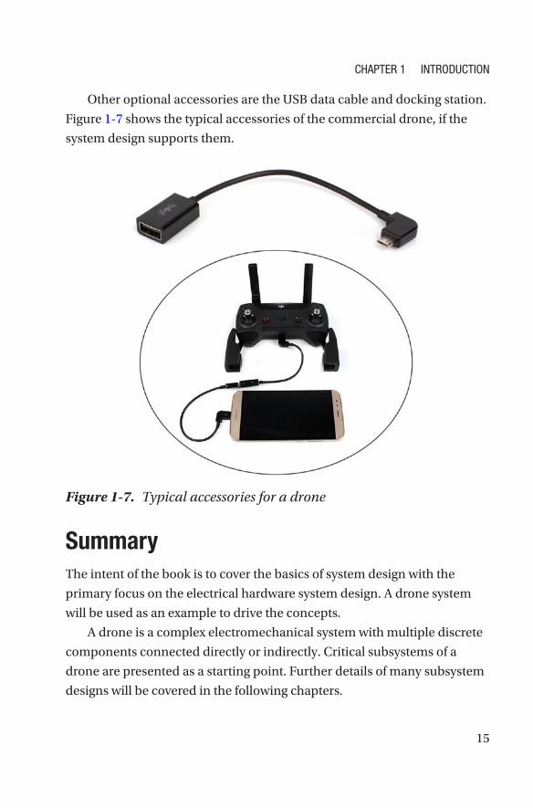
Other optional accessories are the USB data cable and docking station.
Figure 1-7 shows the typical accessories of the commercial drone, if the
system design supports them.
Figure 1-7. Typical accessories for a drone
SummaryThe intent of the book is to cover the basics of system design with the
primary focus on the electrical hardware system design. A drone system
will be used as an example to drive the concepts.
A drone is a complex electromechanical system with multiple discrete
components connected directly or indirectly. Critical subsystems of a
drone are presented as a starting point. Further details of many subsystem
designs will be covered in the following chapters.
Chapter 1 IntroduCtIon

17© Neeraj Kumar Singh, Porselvan Muthukrishnan, Satyanarayana Sanpini 2019 N. K. Singh et al., Industrial System Engineering for Drones, https://doi.org/10.1007/978-1-4842-3534-8_2
CHAPTER 2
Drone System Design FlowIn the previous chapter, you learned about the fundamentals of a drone
system and the integral parts of a drone, which are basically hardware,
software, and mechanicals. You also learned about the subsystems of the
drone and how they map to the features of the drone as a product.
In this chapter, we will primarily discuss the flow of drone system
design. The flow will assist you in the deep learning of the system and its
applications. Design flow starts with the architecture, which includes all
the system elements or blocks, which we will describe in detail in each
section on hardware, software, and mechanicals for a quick understanding
of the cross-functional engineers and any other team that contributes to
the system design.
In this chapter, we’ll focus on the general flow of the system design
with annotations relating to the drone system design. We’ll also define, at
a high level, what example design we will take for illustration purposes.
The details on various stages or steps relating to the specific drone system
design will be covered in the upcoming chapters.
System DesignSystem design, in general, is usually done by a group of experts (or team)
involving expertise from hardware, software, and mechanical engineers

18
with different and complementary skill sets. This group of people typically
consists of component engineers, CAD engineers, design engineers,
test engineers, and program managers. Many times the composition of
the team depends upon the nature of the product being designed and
developed.
In general, the product design process typically involves three main
aspects: specification, architecture, and implementation.
Requirement SpecificationRequirement specification is the first step in any system design. The
requirement specification step involves gathering the requirements and
converting them into detailed document collaterals which act as the
starting point for various teams involved in the design. For a complicated
electromechanical system like a drone, multiple documents from
electrical, mechanical, and software are required to understand
the design.
A single source document, which is accountable to generate all of
the other architectural documents in sequence or parallel, is the product
requirement document (PRD).
The PRD is the scope of the target system, created with input from the
marketing team based on the extensive market research, contributions
from the customer, and input from the engineering team. The engineering
team works in parallel to gather the requirements and collating the
reports and results from feasibility analysis. The PRD can sometimes
be interchanged with the system requirement document (SRD). While
different organizations use different terminology, generally PRD is
the terminology used by the marketing team, external teams, or non-
engineering teams, whereas the term SRD is used by the design team or
engineering team.
Chapter 2 Drone SyStem DeSign Flow

19
ArchitectureThe engineering team generates the engineering specification in response
to the PRD, which addresses the possibility of fulfilling the requirements
of the PRD or a deviation or alternate way of fulfilling the requirements.
There are several other design documents that represent the hardware,
software, and mechanicals at a high level to explain the sections to
external, cross-functional, and customer teams to keep everybody on the
same page before starting the actual design.
Mechanical Design
The mechanical concept is usually done in a CAD (computer-aided
design) tool. The output is usually a standard file format that can be
opened/imported in any CAD application software or multiple image files
showing the sectional view such as top, bottom, and cross-sectional view
of the target 3D model concept. Figure 2-1 shows the partially completed
or work-in-progress 3D model file developed using CAD tools of an
X-frame of a drone. This is not limited to the X-frame; other mechanical
parts like enclosures, screws, and propellers need to be designed in the
same way to complete the 3D model. The electrical components like
the PCB and the interconnects are modeled in a different electrical CAD
tool and are imported into a mechanical CAD tool to get the complete
3D concept of the drone. The dimensions and tolerances of the parts
need to be more accurate for the 3D model in order to avoid any defect
during manufacturing. The mechanical concept is usually a part of the
engineering specification and it presents the opportunities and risks of
meeting the requirements from the PRD.
Although the perfect balance between hardware, software, and
mechanical ingredients is required for an outstanding system design,
one of the key selling points for a consumer drone is the aesthetics of the
mechanical enclosures. Therefore, a lot of focus is on the mechanical
Chapter 2 Drone SyStem DeSign Flow

20
design in the initial phase. Mechanical design, like most other design work,
is an iterative process; that means you start with an initial concept and
then iterate over it based on feedback. Hardware and software go through
the minor changes in the middle or later point of time during the detailed
design phase.
There are different mechanical CAD tools available to develop the 3D
models. Output files are generated in a specific format to easily view using
other applications or viewers. Viewers are the light version of the same or
different CAD tool, and don’t require any license and can be installed on
any hardware with minimum graphics. Usually viewers are used by cross-
functional engineers to view the actual 3D model of the product during the
architecture and design phase. One such example is shown in Figure 2-1.
A completed X-frame step file is viewed using step viewer tool. A step file
is the most widely used file format (.STEP). An ISO 10303 standard format
can represent 3D objects in CAD and related information.
Figure 2-1. A 3D model of the X-frame
Chapter 2 Drone SyStem DeSign Flow

21
The mechanical design process has evolved over last few years with
the rise of 3D printing. New consumer-friendly 3D printers can produce
dimensional objects. The 3D printers print (create) objects with a plastic-
like substance as opposed to traditional printers that spread ink across a
page. Building a prototype from the 3D mechanical model is cooler these
days, unlike hardware design, which still stay as a longer pole in the system
design.
Hardware Design
In the past, new product design and development in the field of electronics
was by definition hardware design. Today, this isn’t the case; it is only a
part of the equation. Hardware design at a concept level or an architectural
level is usually explained with an electrical block diagram with all the
electrical ingredients interconnected through the compatible electrical
interfaces. Generally, all the ingredients are connected to the SOC, which
is often considered the brain of the system. A few ingredients can connect
to each other directly rather connecting to SOC if the ingredients are
independent or the functionality of the specific ingredient demands. The
key list of ingredients required for the system also explains the product
structure at a high level. Figure 2-2 shows the hardware block diagram,
which includes part numbers of the devices used and also completes the
key bill of materials of the hardware. These are the minimum required
hardware blocks to build a drone; more details in the upcoming chapters.
The hardware of the system is nothing but a PCBA. This block diagram
completely transforms into a PCBA, which is discussed in more detail in
the implementation part of this book.
Chapter 2 Drone SyStem DeSign Flow

22
Software Design
In a system, the complete functionality is co-provided by hardware (HW)
and software (SW). Based on the product PRD, HW and SW partitioning
is done. In other words, it shows what part of the functionality is provided
by chosen HW blocks and what is covered in SW. After the partition is
made, the SW design and development can start straightaway. There are
SW design practices and a SW development life cycle that is followed.
The focus of this book is not the software design flow since it’s very well
established and enough references are available relating to SW product
life cycle.
Figure 2-2. Drone hardware block diagram and key BOM
Chapter 2 Drone SyStem DeSign Flow

23
ImplementationThis is where the designers narrow their ideas, which can be guaranteed
successes, and from there they can outline their plan to make the
product. In this phase, the engineers implement the design and build the
prototype as per the plan outlined in the previous step. The last stage of
this phase is when the product is tested, and from there, improvements
are made. The implementation part is explained in detail in upcoming
chapters of this book.
Specifications for Our Drone, “Crop Squad”For the illustration and discussion in this book, we are going to take the
below specification for the design throughout this book. The specification
given in Table 2-1 also corresponds to the architecture diagram given in
Figure 2-2.
Table 2-1. Drone Hardware Specifications
Subsystems Features Specifications
proCeSSing CpU Quad-core 2.34 ghz
memory ram 4 gB
external SD Card 128 gB
internal uSSD 128 gB
Camera hyperspectral
imaging
line scan, 600-975nm, >100 bands
interface: USB 3.1
aUDio alert types Beep, vibration
loudspeaker yes, with stereo speakers(need basis)
(continued)
Chapter 2 Drone SyStem DeSign Flow

24
Mechanical DesignAs mentioned in the previous section, defining (creating) or choosing the
right mechanical design of the system is the starting point. In the following
sections, we will talk about the key aspects of making mechanical design
choices.
A drone is not an entirely new concept. The term was used in the early
1900s for UAVs. Different types of drones are already in use for various
purposes. Keeping that as a base and the target application in mind, a
perfect mechanical design needs to be created that, along with hardware
and software, must fulfill all the requirements listed in the PRD.
The simple drone named Crop Squad is designed for agriculture
applications and is expected to monitor crops, analyze the local crop
health, and upload the reports or upload the raw capture to the datacenter
for further analysis. From the mechanical engineering perspective, there
are specific things to take care of for this drone.
Subsystems Features Specifications
CommS wlan wi-Fi 802.11 a/b/g/n/ac, dual-band,
Bluetooth 4.2, a2Dp, le
gpS yes, with a-gpS, glonaSS, galileo, QZSS
DiSplay hDmi yes
io type C type C USB3.1 for data communication, charging
SenSorS Sensors accelerometer, gyro, proximity, compass,
barometer
otherS Fpga Flight controllers, embedded controllers, motor
pwm controllers
Table 2-1. (continued)
Chapter 2 Drone SyStem DeSign Flow

25
What are the typical mechanical requirements of Crop Squad to fulfill
this application?
1. A quadcopter to fly high to cover or get a view of a
larger area of the agricultural land
2. A hyperspectral imaging camera to capture the
patterns or other observations of the crops (leaves,
stems, and pods) periodically
3. A high-speed wireless network to upload the raw
image capture back to the datacenter for further
processing and analysis or to analyze locally if the
drone is equipped with a high computing processor
4. A remote controller to operate the drone from a
remote location or equip the drone with artificial
intelligence (AI) to do the job independently
without any control
At a high level, the requirement looks simple, with four variables:
quadcopter, camera, wireless network, and remote. But creating a
mechanical design is not as simple as that; numerous variables come into
the picture. The mechanical design also depends on the creativity of the
individuals. While the form factor or aesthetics of a product (including a
drone) are driven by industrial design and marketing, design engineers
usually have to apply a lot of creativity and ideas of innovation in meeting
the requirements.
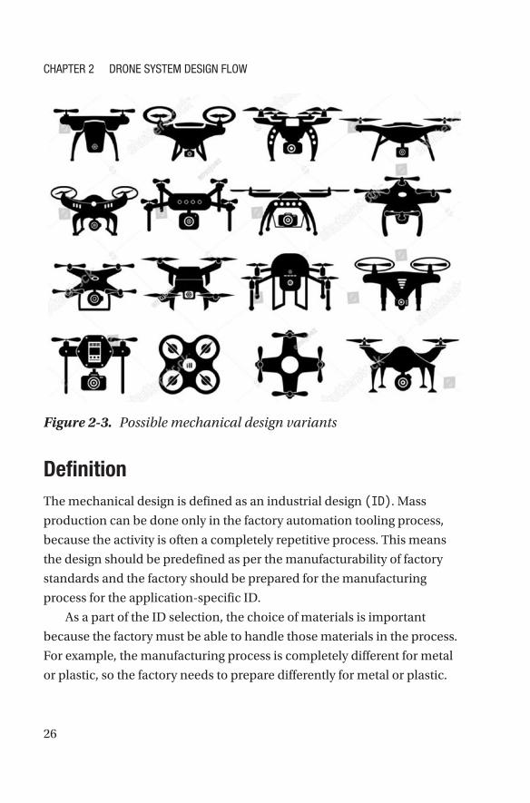
Figure 2-3 shows the different types of mechanical designs that can
be created for the requirements mentioned above. Each drone design
is unique and it’s up to designer to decide which design best suits their
application.
Chapter 2 Drone SyStem DeSign Flow
26
DefinitionThe mechanical design is defined as an industrial design (ID). Mass
production can be done only in the factory automation tooling process,
because the activity is often a completely repetitive process. This means
the design should be predefined as per the manufacturability of factory
standards and the factory should be prepared for the manufacturing
process for the application-specific ID.
As a part of the ID selection, the choice of materials is important
because the factory must be able to handle those materials in the process.
For example, the manufacturing process is completely different for metal
or plastic, so the factory needs to prepare differently for metal or plastic.
Figure 2-3. Possible mechanical design variants
Chapter 2 Drone SyStem DeSign Flow
27
An X-frame of the drone can be made from plastic or metal. A plastic part
and a metal part need to be designed differently, and the factory process is
likely to change based on the material.
With all other things being the same, the ID is one of the key deciding
factors since it creates the first impression with the customers, and a
favorable impression increases product sales.
PurposeThe PRD lists the high-level applications of the drone. It’s the engineer’s
responsibility to learn the next level of details and understand the actual
purpose of the drone. For example, Agriculture is the broad area where
drones are used for soil and field analysis; to spray the seeds; and to
irrigate, monitor, and collect health report of the crops.
If a single drone is designed for all of the above mentioned purpose,
the ID and system design will be complex. Even if the system is designed
to perform all of these tasks, the design will overload and the system CPU
unit may not support multiple parallel activities with the current available
technology. Instead, a single drone can be designed to fulfill a combination
of two or three applications together. The engineer has to clearly mark the
abilities of the drone being built.
Figure 2-4 shows the drone mounted with a hyperspectral camera
used to monitor crops. The same drone cannot be used for soil and field
analysis and for spraying water or seeds unless equipped with relevant
modules inside.
Chapter 2 Drone SyStem DeSign Flow

28
RequirementsOnce the purpose is known, the engineer can convert the PRD to next-
level detailed mechanical requirements for an ID, including hardware and
software.
The PRD and the purpose trigger the engineer’s creativity and give
birth to a brand new drone design. The engineer works with a cross-
functional team for the materials required, size, and shape of the ID.
The PCBA is considered as a single mechanical part from the hardware
team. The dimensions of the PCB are the most important requirements
from the hardware engineers to complete an ID. Some other requirements
are battery dimension, antenna position, and IO connector placement.
Figure 2-5 shows the typical stack-up of mechanical parts in a drone
ID. This is also the cross-sectional view of the mechanical design of the
drone, and the significance of each part is explained below. This stack-up
may differ for drones in different applications.
Figure 2-4. An agriculture drone used to monitor crops
Chapter 2 Drone SyStem DeSign Flow

29
1. Propeller: Angled blades attached to the revolving
shaft of a motor. These blades gives thrust and are
why the drones can fly high.
2. Propeller motor: This is a DC motor attached to the
four corners of the X-Frame. Power from the drone’s
electrical system rotates the blades to provide thrust
to the drone.
3. Enclosure top: A plastic or fiber mechanical
enclosure of the drone protects the internal
electrical and mechanical subsystems from the
external disturbances. Enclosures also provide the
aesthetic look for the drone as a product.
4. X-frame: This is the vertebra of the drone. All of the
other mechanical parts and subsystems of the drone
are attached to the X-frame through different types
of fasteners or ties. The X-frame is symmetrical by
dimensions and weight on all sides to achieve a
balanced flight of the drone. So the cross-sectional
view is symmetrical on Y axis.
Figure 2-5. A typical drone system stack-up
Chapter 2 Drone SyStem DeSign Flow

30
5. Enclosure bottom: A plastic or fiber mechanical
enclosure of the drone protects the internal
electrical and mechanical subsystems from the
external disturbances. Enclosures also provide the
aesthetic look for the drone as a product.
6. Mylar: A form of polyester resin used to make
heat-resistant plastic films and sheets. It acts as an
insulation layer between the conductive layer of the
PCBA and the metallic X-frame.
7. MB (motherboard): The PCBA of the system hosts
all of the electrical parts of the system soldered on to
it. By modifying the PCBA shape, the same layer can
accommodate the battery on the sides of the PCBA.
8. CPU: Usually an SOC, it’s the processing unit of the
system. All other devices soldered on the PCBA are
on the same layer adjacent to the CPU.
9. Shielding and TIM: Digital and RF devices usually
need shielding to protect from external disturbances
or to protect the external devices through radiation.
Radiation from the external world is suppressed by
connecting the shield to a system ground.
The TIM, thermal interface materials such as
graphite, is pasted as a thin layer on the shield
to radiate the excess heat generated from the
components of the system.
10. Heat spreader: The heat exchanger that moves
heat between a heat source and a secondary heat
exchange, whose surface area and geometry are
more favorable than the source.
Chapter 2 Drone SyStem DeSign Flow

31
11. Air gap: Provided wherever necessary in a
system. This air gap acts an insulator and also
accommodates material expansion and contraction
due to unavoidable reasons in a system.
12. Camera module: The lower-most part of the
drone in this application is the camera module.
Attached on the bottom to get a better field of view
(FOV) when drone fly high. Most camera modules
accommodate ISPs and connect to the SOC through
the USB 3.1 interface. If the SOC has integrated ISPs,
then the camera sensor can directly connect to the
SOC with camera-specific interfaces.
13. DB (daughterboard): If all of the ingredients can’t
be accommodated in the single PCBA, then there
can be several daughterboards on the system to
accommodate additional ingredients. Motherboards
and daughterboards can be connected through
board-to-board interconnections or a flex PCB
interconnect. In this drone, the WiFi+BT module
cannot be kept below the X-frame. The metal
X-frame might obstruct the signal for the module’s
embedded antenna. Alternatively, the module can
be kept in the same PCBA with the external antenna,
which may not be good for an ID.
14. FPC (flexible PCB): Generally used to connect one
or more rigid PCBs in a complex system.
Chapter 2 Drone SyStem DeSign Flow

32
DependenciesAlthough the engineer’s creativity and ideas produce an attractive ID, the
discrete components, subsystem location, and other dependencies can
limit her ideas from becoming a reality.
Multiple discrete components such as the X-frame, motors, propellers,
PCBA, screws, gaskets, enclosures, batteries, FPCs, and cables integrate
through various electrical and mechanical interconnects in an ID. Apart
from the discrete mechanical components, there are electrical subsystems
located on the PCBA, which largely impact the design of the ID.
For example, the position of the power and IO connectors determine
the front, back, top, and bottom view of the ID. Usually IO connectors are
placed on the back or bottom side of the ID to make them invisible to the
user. Also, the presence of wireless components prominently affects the
ID design. The antenna is the most vital part of the wireless interface and
its placement varies for the mobile network, WiFi, and other RF remote
control technologies.
With all of the above mentioned challenges, the mechanical team has
to come up with best ID for the product.
Hardware DesignThe process of converting the Figure 2-2 block diagram or hardware
architecture to a fully functional PCBA is called hardware design.
The hardware design fundamentally focuses on getting the desired
functionality to the system. PCBA development starts with the hardware
requirement capture based on the PRD, followed by ingredients selection
and choice of the right PCB to interconnect the ingredients, and finally, the
power architecture, design, and implementation for the hardware.
The PCBA is considered as a single discrete mechanical part in an ID.
Subsystems and other ingredients of the PCBA are part of the electrical BOM.
Chapter 2 Drone SyStem DeSign Flow

33
Hardware RequirementsThe first step in hardware design is the understanding of the hardware
requirements. Hardware requirements may vary depending on the
operating system and the overall system design, which is usually covered
in the PRD.
There are variations possible for a system providing similar
functionality. For our case, there could be different variations of
drones possible, but still providing the functionality we outlined. The
differentiation comes from the parts that are chosen in the system.
Generally speaking, there are different modules that can provide certain
functionality. However, there may be differences relating to, for example,
the power, performance, latency, and durability of those components.
Generally, there are minimum hardware specifications of the devices,
which barely meet the requirements. If the system is built with these
devices, it’s a low-end product. A low-end product usually lacks speed
and quality. So it is the one of the cheapest in the product range or on the
market as a whole.
Above minimum requirements, there are recommended specifications
for the effective operation of the operating system. Products with these
specifications fall in the medium range in terms of cost and quality.
Also, there is a higher end to the hardware specifications of each
device, under which the system will operate at high performance. So the
product is one of the most expensive or advanced in a product range or on
the market as a whole.
It is typically the hardware or the devices used that define whether the
system is a low-end or high-end product. Table 2-2 shows the hardware
requirements of the drone.
Chapter 2 Drone SyStem DeSign Flow

34
Table 2-2. Drone Hardware Requirements
Features Key Component Requirement
Proposals Dependencies
CpU Quad-core 2.34 ghz Quad-core 2.34ghz required
memory 2gB lpDDr3 4gB lpDDr3 required
Storage 64 gB uSSD 128gB uSSD required
Camera 600-975nm, line scan,
hyperspectral imaging
470-900nm, line scan,
hyperspectral imaging
required
wiFi 802.11 1x1 ac module m.2 12*16 802.11 1x1
ac module
required
Sensor accelerometer, ambient
light, gyroscope,
temperature, altitude,
pressure
accelerometer, ambient
light, gyroscope,
temperature, altitude,
pressure
required
io ports 1xUSB type C
1xuSD4.0
1xuSim
1xpowerJack
required
mobile network lte m.2 lte module optional
Fpga
pCB 12-layer hDi 8-layer hDi required
power integrated integrated required
Charger 7.4V, 5a 7.4V, 5a required
Battery 10000mahr 10000mahr required
DC adapter 12V, 3a 12V, 3a required
Chapter 2 Drone SyStem DeSign Flow

35
Electrical Ingredients SelectionAs explained in Chapter 1, the detailed electrical feature set of the system
is directly related to the electrical ingredients of the PCBA. Selection
of ingredients is based on the detailed analysis of the current available
technologies and anticipated technological developments. Usually, the
ingredients supplied by different vendors vary in terms of cost, package,
technology, and lead time based on factory production capabilities.
All the ingredients selected should adhere to the technology used in
the SOC. The SOC as a central processing unit connects all the ingredients
as peripherals of the system. Table 2-1 shows the list of electrical
ingredients of the system. The same list will become the key component
of the bill of materials, with the addition of the manufacturer and
manufacturer part number details.
BOM and Component Procurement
The bill of materials is a list of components required to build a system
or product. It includes raw materials, subassemblies, intermediate
assemblies, subcomponents, parts, and the quantities of each needed
to manufacture an end product. A component may be used for
communication between manufacturing partners, or confined to a single
manufacturing plant. A bill of materials is often tied to a production order
whose issuance may generate reservations for components in the bill of
materials that are in stock and requisitions for components that are not in
stock.
The list of materials required to build a system or a product is called a
system BOM. A system BOM is usually hierarchical in nature with multiple
levels. Each component in a BOM or subassembly in the main can be
called a child item of the main BOM.
Chapter 2 Drone SyStem DeSign Flow

36
Similarly, the list of components or materials required to build a PCBA
is called an electrical BOM (EBOM). The EBOM is a part of the system BOM
in most systems and is one of the child items of the main BOM.
In general, the electrical components are selected based on the
following key parameters:
• Availability: Availability is usually a development
schedule of the part. Design, build date, quantity,
and lead time of the part should match the project
schedule.
• Production status: The production status should be
active when the final product is built. Inactive or end-
of- life (EOL) samples are recommended for a new
design. At the very least, engineering samples should
be available during the design phase, if not production
samples.
• Cost: Cost is a key factor to be negotiated with the
manufacturer to get the overall target BOM cost as low
as possible.
• Operating temperature: Each ingredient falls under
different temperature grades like commercial,
industrial, and defense. The cost will increase if the
operating temperature range increases.
Note the widely accepted operating temperature range for commercial is – 0 to 60, for industrial is -40 to 85, and for military is -55 to 125.
• Storage temperature: The temperature at which
devices/products are stored, typically ambient
temperature.
Chapter 2 Drone SyStem DeSign Flow

37
All of the parts shown in Figure 2-5 are child items of the system
BOM. Reservations should be placed for the parts that need to be procured
from the third party-vendors. Custom-built parts like the X-frame,
enclosures, head spreader, PCBA, etc. are done at the OEM/ODM factory
facility by preparing the factory specific to the drone project.
An OEM (original equipment manufacturer) is a company that
manufactures the drone; it is marketed with a different manufacturer’s name.
An ODM (original design manufacturer) is a company that designs
and manufactures the product as per the specifications; the product is
rebranded by another company for sale.
PCBA DesignThe PCBA design is the extended process in the system design. Some
degree of pre-work needs to be done during the architecture phase. More
details will be explained in the upcoming chapters
To select the right PCB for a system, the following parameters need to
be examined:
1. PCBA dimensions
2. PCB type
3. PCB layer stack-up
PCBA Dimensions
The target length, width, and thickness of the PCBA are derived from the
mechanical design. All of the ingredients need to be accommodated in the
given length, width, and height of the PCB. Figure 2-6 illustrates the PCBA
dimension.
In this design, the Crop Squad drone is the size of a mid-sized
commercial drone. This PCB is approximately less than a size of the credit
card, which is 85mm X 54mm. The target PCB dimensions slightly vary
Chapter 2 Drone SyStem DeSign Flow
38
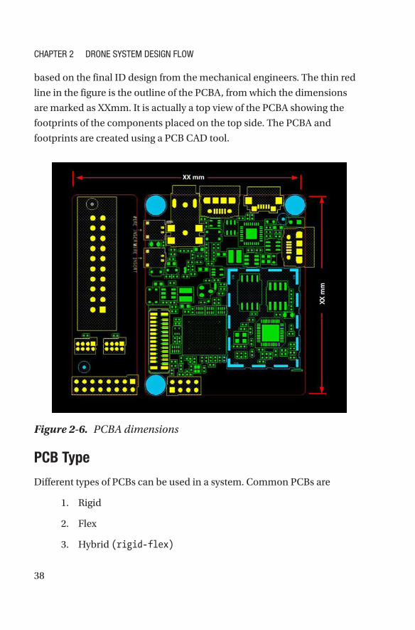
based on the final ID design from the mechanical engineers. The thin red
line in the figure is the outline of the PCBA, from which the dimensions
are marked as XXmm. It is actually a top view of the PCBA showing the
footprints of the components placed on the top side. The PCBA and
footprints are created using a PCB CAD tool.
Figure 2-6. PCBA dimensions
PCB Type
Different types of PCBs can be used in a system. Common PCBs are
1. Rigid
2. Flex
3. Hybrid (rigid-flex)
Chapter 2 Drone SyStem DeSign Flow

39
Rigid PCBs are most preferred. Flex PCBs are used in a complex
systems where rigid PCBs do not fit.
In the Crop Squad drone, shown in Figure 2-1, the architecture
diagram of the SSD and WiFi Bluetooth modules are placed on a separate
board and are connected to the main board through a FPC connector.
This shows that the electrical part of the drone is split into two rigid PCBAs
connected through a flexible PCB. The idea is to keep the WiFi module on
a separate PCB to avoid the obstruction of the embedded antenna by the
metallic X-frame and to eliminate the need of any external antenna.
In some systems, a rigid PCB breaks into small pieces and is
interconnected through the flexible PCBs without any external
interconnect, which is also called a hybrid PCB.
Figure 2-7 shows two rigid PCBs interconnected with a flexible
PCB. This figure clearly shows that rigid PCBs cannot be folded, whereas
flex PCBs can be folded any direction with minimum bend radius.
Figure 2-7. Hybrid PCB
Chapter 2 Drone SyStem DeSign Flow

40
Layer Stack-Up
A PCB can be single-sided or double-sided. A single-sided PCB is one
that has components placed on one side (top or bottom), whereas a
double-sided PCB has components on both the top and bottom side.
The advantages of a single-side PCB is low cost manufacturing and easy
assembly. No air gap is required for the non-component side inside a
mechanical assembly. The manufacturability and assembly cost is high
for a double-sided assembly and an air gap is required on both sides in a
mechanical assembly, since both sides are mounted with components.
In a complicated system, multiple conductive and dielectric layers are
sandwiched and laminated in between. Layer count, copper plane, and
dielectric thickness decide the overall thickness of the PCB.
The number of power rails in a system is directly proportional to the
power layer count. Signal count, trace width, and density of the high speed
and low speed signals determine the signal layer count of the PCB.
The power and signal from different layers are connected through
“vias” (drills filled with copper perpendicular to the PCB
plane connecting the conductors of the layers). A standard PCB
has through hole vias covering the top layer to the bottom layer. An HDI
(high-density interconnect) PCB has multiple via structures such as
a micro via or a stacked via (connects only two adjacent layers), a
buried via (connects internal layers not exposed to any external
layers), a blind via (connects the top layer to the next layer
under a component) and a through hole via.
PCB stack-up is an important factor in determining the EMC
performance of a product. A good stack-up can be very effective in
reducing radiation from the loops on the PCB (differential-mode
emission), as well as the cables attached to the board (common-mode
emission). On the other hand, a poor stack-up can increase the radiation
from both of these mechanisms considerably.
Chapter 2 Drone SyStem DeSign Flow

41
Figure 2-8 shows partial layer stack up of 3-6-3+ PCB with buried
vias (4-9) connecting 6 internal layers, a through hole via (1-12) connecting
all 16 layers, and a micro via or stacked via connecting the adjacent layers
for the top 4 and bottom 4 layers. The first column of the table shows the
layer name (i.e. signal or power). The signal layer is the layer in which the
actual signal with specific impedance is routed. The power layer is made
up of one or more copper planes that carry different power supplies for ICs
on the PCBA. The second column shows the layer type. The layer type is
either a conductive layer with thickness mentioned in ounces along with
conductive plating as “1/3oz+plating” or a dielectric layer with material
properties mentioned as “PP1067/1078.” The other two columns show the
thickness of each layer and tolerance in millimeters. The last column in the
stack-up is the dielectric constant of the dielectric materials. In general,
the stack-up will have a few more columns, including the trace width of the
signal to achieve the target impedances.
A detailed feasibility study needs to be done to select the right PCB
layer stack-up. Usually floor planning along with a route study is done
with a minimum layer count by the combined effort of electrical design
engineers and CAD engineers to arrive the right stack-up.
In Figure 2-2, there are high-speed electrical connections on the PCB
such SATA, USB3.1, HDMI, and PCIE. Considering the size of the board
and the density of the high-speed signal, the design may require 6 signal
layers and 6 power layers based on the initial assessment.
Via arrangements are decided based on the signal and power layer
arrangement. In this stack-up, the top 4 and bottom 4 layers can be
interconnected though a micro via. The 3-x-3+ mentioned in the stack-up
is a micro via on the first and last 3 layers plus an additional layer. Then the
center x number of layers are connected though a buried via.
Cost is an important factor and plays a key role in deciding the stack-
up. So many factors affect the cost of a PCB; for example, in the layer
Chapter 2 Drone SyStem DeSign Flow

42
stack-up in Figure 2-8 there will be significant cost reduction by reducing
the layer count, via pattern (removing the blind and buried vias will
significantly reduce manufacturing cost). It is up to the designer to choose
the optimum and correct stack-up for the design. The PCB stack can be
changed throughout the hardware design phase before we release the
design files for PCB fabrication. These PCB fabrication files also called
Gerber files. More details on this in upcoming chapters.
Figure 2-8. PCB layer stack-up
Chapter 2 Drone SyStem DeSign Flow

43
Floor PlanPlacement of the electrical ingredients on a given PCB area is controlled
by SOC placement. SOC interfaces are distributed in such a way that they
connect the ingredients that are placed around. All of the ingredients
placed around the SOC need to be connected with shorter traces due to
restrictions in the routed interface length. Figure 2-9 shows a typical floor
plan of a PCB with the SOC in the center and other electrical ingredients
around. (The floor plan shown is only for illustration purposes and does
not correspond to the drone architecture in Figure 2-2.)
Figure 2-9. SOC, peripheral device, and connector placement
Chapter 2 Drone SyStem DeSign Flow

44
The floor plan also includes the height of the PCB, a major
dependency for the mechanical design. Electrical ingredients placed on a
PCB vary in height, and the mechanical design needs to account for each
and every component. Generally, inductors and capacitors are the tallest
electrical components in the PCBA. Also, high-power consumption
devices dissipate more heat, and these power dissipating devices need
cooling systems. The cooling systems, such as heat sinks and fans, are
the non-electrics parts considered part of the PCBA and they add to the
overall height of the PCBA.
Power ArchitectureThe energy consumption and the battery life have become critical system
parameters. The early estimation of maximum system power consumption
is necessary to design a more efficient power supply.
Battery-operated systems generally have different power states. This
power state is more specific to the use cases of drones. Drone system
power consumption drastically varies for each power states. Drone
system idle is a power state in which all subsystems are on, without any
activity. This is a state where the drone is grounded and thus not in the
air. Standby is the power state in which the system consumes the lowest
possible power. A drone in flight with video recording is the highest power
consumption state and it drains the battery at the fastest rate.
Note System idle, active flight, video recording, sleep, and standby are the different power states a system can support. not all the power states may be applicable for a system.
The power map is the simple representation of the power architecture.
Generally, the power map represents only the maximum power
consumption state of the system.
Chapter 2 Drone SyStem DeSign Flow

45
Power Estimation
In any hardware design, the components in the PCBA are broadly
classified as active and passive devices. Active devices are the components
that consume energy. All ICs are active devices whereas inductors,
capacitors, resistors, and diodes are passive devices that do not need any
power for operation. ICs such as SOCs and other subsystem devices need
more than one power supply (also called a power rail). Generally ICs have
a core rail and IO rails, and core rails consume more power than IO rails.
More details on the power consumption of the devices are discussed in
following chapters.
The power consumption details of each device need to be extracted
from the datasheet of the device. The datasheet states the absolute and
recommended maximum voltage and current specs of the device for all
power states.
In most designs, the number of power rails required for the platform is
equal to or more than the required rails of SOC. Considering the SOC and
platform requirements are equally complicated and the design demands
different power sequencing for the SOC and the platform. Keeping the
SOC and platform requirements separate will make the calculation simple.
SOC Power Requirements
Table 2-3 shows the SOC voltage and current requirements. The SOC itself
as system on chip with multiple functional unit blocks requires different
voltage and current to operate. A typical SOC has functional unit blocks
such as core, graphics, memory, clock, PLL, display, camera, high-speed
IO, low-speed IO, etc. Each block’s voltage range and current consumption
is listed in the table.
Appropriate power devices need to be selected based on the voltage
and current requirement. The power supply should meet the voltage
tolerance (±5% for 3.3V and ±3% for 1.8V) level mentioned in the datasheet
Chapter 2 Drone SyStem DeSign Flow

46
of the each device. The power supply design should accommodate the
appropriate filter circuits to eliminate the ripple and noise from the power
supply before feeding into the devices. Ripple and noise can be reduced by
arranging the power layers in the stack-up as well. Other ways of reducing
the ripple are by placing the power components in the right location and
implementing the best-known power routing techniques.
In new generation SOCs, each functional unit block can be individually
power-gated, which means if any block is unused or inactive, it can be
switched off completely to save power.
Table 2-3. SOC Voltage and Current Requirements
SOC Power 3.3V±5%
1.8V±3%
1.35V±3%
1.2V±3%
1.0V±3%
0.7−1.1V
Core 3000
graphics 5000
logic 1800
l2/l3 2200
memory 1200
Display io 300 300
CFio 500 200
SDio 93
USB 200
total 593 500 1200 500 2200 9800
Chapter 2 Drone SyStem DeSign Flow

47
Platform Power Requirements
Similar to the SOC, there are multiple other devices on the platform that
have different voltage and current requirements. These devices spread
across the platform, and the few devices requiring common voltage can be
switched on simultaneously without any sequencing. Table 2-4 shows the
platform voltage and current requirements.
Multiple subsystems need same the voltage. For example, display,
sensors, camera, and modem are different subsystems and require
common 3.3V with different current requirements and with no specific
sequencing (all the subsystems can be switched on simultaneously).
The platform has multiple power gates for each device to enable/
disable power for the device when not in operation, similar to the SOC,
where each block can be power-gated internally to save power.
Table 2-4. Platform Voltage and Current Requirements
Subsystem Ingredients 5.0V 3.3V 1.8V 1.35V 1.2V
memory lpDDr3 1200
Storage uSSD 300
Ui Display, 100
camera, 900
sensors 10 10
CommS modem, 500
gpS 150
wi-Fi/Bt, 400
Fpga Fpga 500
USB 2.0, 3.0 1400
total 2300 1760 310 0 1200
Chapter 2 Drone SyStem DeSign Flow

48
Power Devices
The previous section listed the voltage, current, ripple, and noise
requirements for the SOC and platform. The total number of voltage
rails for the SOC and platform combined and the total calculated current
consumption for each rail in the SOC and platform helps the engineer to
choose the right power devices for the system. Most power devices fall into
two categories: linear and switching regulators.
Linear Regulators
A linear regulator operates by using a voltage-controlled source to force
a fixed voltage to appear at the regulator output terminal. The most
commonly used linear regulator is the low dropout (LDO) regulator. The
difference between the input voltage and the generated output voltage is
the dropout voltage. The product of the dropout voltage and the current
consumed by the device at the output of the regulator is the power
dissipated at the source. Basically, low dropout voltage and less current
consumption are the desirable parameters when selecting an LDO.
Switching Regulators
Switching regulators operate by switching on/off a series of devices. A FET
will be switched on/off by a pulse width modulation (PWM) controller
transferring energy to load. When the switch is on, energy is stored on an
inductor and capacitor and is also supplying to load. When the switch is
off, the stored energy is discharged to the load until the voltage reaches
the minimum required threshold of the load device. The on/off is done in
a specific duty cycle to keep the output voltage within the tolerance level
of the load device. There are different types of switching regulators: buck,
boost, and buck boost regulators.
Chapter 2 Drone SyStem DeSign Flow

49
Choosing the Best Regulator
The best regulator can be determined by evaluating the parameters listed
in Table 2-5.
Table 2-5. Comparison of Linear and Switching Reguators
Parameters Linear Switching
Function only steps down. input voltage must
not be greater than the output voltage.
Step up, step down,
and inverts
efficiency low to medium high
Complexity low medium to high
Size Small to medium large
Cost low medium to high
ripple/noise low medium to high
Function: Most designs convert high voltage to low voltage. Buck is
desirable, and can be either a linear or switching regulator. If any design
demands low voltage to high voltage conversion, then the regulator choice
is a switching regulator. For example, USB powered systems have 5.0 volts
as the main input, but some systems, like displaying black light, need a
higher voltage to operate. In this case, a boost regulator is required to up-
convert this 5.0 to a higher voltage.
Efficiency: There is no control over the efficiency of the linear regulator.
The product of the load current and the difference in the input and
output voltage gives the power dissipation of the device. For this reason,
linear regulators cannot be used for high load current (the load current
limit depends on the dropout voltage and max thermal dissipation of the
device). But switching regulators can be used for higher current loads and
efficiency can be increased by carefully selecting the external components
Chapter 2 Drone SyStem DeSign Flow

50
like low RDS on MOSFETs, low DCR inductors, and low ESR capacitors.
For better efficiency, go for switching regulators.
Complexity: A linear regulator is very simple. Less external
components are required for stable operation and easy implementation,
whereas the switching regulators are complex, due to the external
components dependencies. More accurate calculations are required when
selecting the components for stable operation.
Size: Linear regulators occupy less space in the board, while switching
regulators need more space on the board to accommodate the PWM
controller, external MOSFETs, inductors, capacitors, and other analog
components.
Cost: The architecture of the linear regulator is simple so the cost is
less. The switching regulator cost is high considering its advantages of high
current and better efficiency in a complex device architecture. On top of
the device cost, the switching regulator needs external components for
normal operation, so the overall cost is multiple times higher than that of a
linear regulator.
Ripple/noise: Ripple and noise are lower in a linear regulator; this
quality makes the linear regulator more suitable for analog designs and
clock and PLL blocks in the SOC. Switching regulator outputs are noisier
than linear ones even with multistage filters.
Power Map
The previous section explained the pros and cons of the switching and
linear regulators. Linear or switching regulators need to be selected for
multiple power rails of the SOC and platform. Among the power rails,
some need to be always on and some need to be power-gated whenever
the system goes to sleep or the subsystem is inactive for some reason. Also,
there are different power sequencing requirements for the SOC, platform,
and other devices if specified in the datasheet.
Chapter 2 Drone SyStem DeSign Flow
51
All of the requirements for power consumption, power gating, and
sequencing on a power map are drawn for easy understanding and are
converted to an actual design of circuits. Figure 2-10 illustrates the power
map, which will be converted to power design in schematics and then into
a PCBA.
Generally, the initial power map may not be accurate with the drone
architecture. It may go through significant changes on the later part of the
design based on the requirements of the electrical specifications of the
ingredients. A very complicated power architecture can be explained in a
simple way using a power map. From a landscape view, the items on the
left are
1. Source is the type of regulator used to deliver the
power. For example, Buck, Buck1… Buck6 are
switching regulators used to deliver higher load
currents delivering multiple loads together. ALDO,
DLDO, and GPLDO are LDOs delivering lower
currents either for single load or multiple loads.
2. Rail Name is the name of the connection used on
the board to differentiate from one another. Multiple
3.3V will be delivered from multiple sources to
multiple loads. Connections should be used to
distinguish names to avoid a short circuit on the
PCBA.
3. Voltage is the voltage level or the range the source is
delivering.
4. Imax is the maximum load current the device will
support or specified by the vendor in the datasheet.
5. Iload is the maximum current the device is actually
loaded by the subsystem connected to in the design.
Chapter 2 Drone SyStem DeSign Flow

52
On the top side of the power map are the details of the SOC blocks
and subsystems (camera, display, memory, modem, etc.); current
consumptions are listed. The power map also shows the connections
from the power supply devices to the subsystems and distribution along
the platform. The representation of power distribution in a map makes
the conversion easy for schematics and layout. Every connection in the
power map will become a trace on a PCB. The current consumption
values mentioned in the power map will help to calculate the power plane
thickness and power trace width in PCB.
Figure 2-10. System power map
Chapter 2 Drone SyStem DeSign Flow

53
Power Sequencing
Powering up a circuit on a printed circuit board is too often taken for
granted and can cause damage and both destructive and nondestructive
latch-up conditions. These problems may not be prominent until volume
production begins, when the tolerances of devices and designs are put to
the test. This is dangerously late in the process and extremely expensive
with respect to time and the delivery of projects and products. Errors
found at this stage result in numerous modifications, including PCB
layout changes, design alterations, and extra anomalies. With the advent
of incorporating many functional blocks into one integrated circuit (IC),
this results in supplying these blocks with multiple, sometimes equal, or
in many instances, differing voltage supplies. As more and more of these
SoC ICs proliferate the marketplace, the need for particular power supply
sequencing and power management issues arises. There is usually enough
information on device datasheets to guide a designer to a correct power-
up sequence for an individual IC. However, some ICs specifically require
a well-defined power-up sequence. This is true in the case of many of ICs
and is quite common in ones using multiple supplies such as converters
(consisting of both analog-to-digital converters (ADCs) and digital-to-
analog converters (DACs)), digital signal processors (DSPs), audio/video,
radio frequency, and many other mixed signal ICs. Essentially, any IC
containing some analog input/output with a digital engine falls into this
category, where particular power sequencing may be required. On these
ICs, there could be separate analog and digital supplies and some may
even have a digital input/output supply, as detailed in specific examples
discussed in the following sections. Some of the more common supplies
presently are +1.8 V, +2.0 V, +2.5 V, +3.3 V, +5 V, −5 V, +12 V, and −12 V.
Figure 2-11 shows a typical power sequencing requirement of the SOC.
Table 2-6 shows the timing details of the each power in microseconds.
Chapter 2 Drone SyStem DeSign Flow

54
Figure 2-11. SOC power-on sequence
Table 2-6. SOC Power Sequencing Numbers
Symbol Description Min Max Units
tvin +V3p3a stable power after +5pa USB power 0 na us
tvddio +V1p8a stable power after +3p3a 100 na us
tvdd +V0p9a stable power after +V1p8a 100 300 us
tclkin Clock active after +V0p9a stable 100 na us
trst host reset assertion after clock 10 na us
trst_width host reset active time 10 na us
tirq host interrupt assertion after deassertion of host rest 50 200 us
Chapter 2 Drone SyStem DeSign Flow

55
Battery Estimation
Batteries are energy storage devices that are particularly useful for
powering small portable devices like phones, laptops, and entertainment
devices as well as mobility devices that travel over the Earth’s surface,
through water, and in the air.
Battery Constraints
The batteries used in these applications are engineered to meet the
unique design constraints imposed by these different applications. These
constraints are covered in the following sections.
Number of Cells or Voltage
The term “battery” refers to a system of one or more cells. A cell represents
a particular chemical combination capable of producing a voltage and a
current. Different chemical combinations produce different voltages. By
combining cells in series, the voltage of a battery pack can be increased as
a multiple of the number of cells x the voltage of each cell.
Battery Chemistry
A rechargeable battery is referred to as a storage battery and is usually
constructed of one or more secondary cells. Each cell is capable of
producing a specific voltage with respect to the electrochemical makeup of
the cell. Batteries store energy through changes in their internal chemistry.
When a battery is discharged through a load like a circuit or a motor,
the internal battery chemistry undergoes a change. When the battery is
charged, the chemical change is reversed, and the energy is again stored
in the battery. A specific amount of energy can be stored in a battery given
the specific battery chemistry, the configuration of the battery, and the
battery volume and weight.
Chapter 2 Drone SyStem DeSign Flow

56
Cell Voltage and Battery Packs
For NiCad/NiMH, cell voltage is about 1.2V; for lead acid, it is 2.0V; and
for lithium cells, it is on the order of 3.6V. Typically, portable electronic
devices are designed to run on 12, 24, 36, or 48 voltages. To create these
voltages, a number of cells are connected in series in order to form a
battery that has the desired net voltage.
Battery Capacity
Battery capacity is published by the manufacturer as a nominal rating for a
given set of discharge conditions. These discharge conditions include rate
of discharge (C rate), temperature, and minimum cell voltage. Minimum
cell voltage is the lowest voltage to which a cell or battery should be
charged. Discharging a cell or a battery below the minimum voltage can
reduce or even destroy the battery’s capacity to hold a charge.
Battery performance parameters can include voltage, amp-hour
capacity, and C rate (rate of discharge).
The C rate refers to the amount of current the battery can sustain for an
hour while remaining within a specified voltage range. For a typical 12 volt
battery, this voltage range is between 12 volts and 10.5 volts for the battery
to be considered fully charged.
Typical units of battery capacity are expressed as a milliamp-hours or
mA*h; for larger batteries, it is amp-hours or A*h. This rating implies the
discharge rate in amperes that the battery can be expected to sustain for a
period of one hour.
Battery capacity varies with the discharge rate. When you discharge
a battery at higher rates, the amp-hour capacity of the battery will be less
than the nominal or published capacity.
Battery capacity is measured in amp-hours (Ah). A pack that can deliver
1 amp for 1 hour has a capacity of 1 Ah. The battery capacity is usually
given by the manufacturer in amp hours (Ah) or milliamp hours (mAh).
Chapter 2 Drone SyStem DeSign Flow

57
Suppose a 15lb drone with four motors draws an average of 4 amps
for video recording on the flight. If you fit a 4 Ah battery pack, it can be
expected to run for one hour on average.
Watt Hours and Energy Density
There are two different ways of indicating battery capacity: you can use
either AHr (ampere hour) or WHr (watt hour) for battery life calculations.
And both approaches are used in product designs. The WHr approach
is more comprehensible. The watt-hours stored in a battery pack are
approximated by multiplying the rated amp-hours by the pack voltage.
Energy density usually refers to the energy in watt hours per unit mass
of the battery. The energy available from a given battery can be estimated
using the manufacturer’s published data for a given battery pack or cell.
The information needed to calculate the energy density can also be
obtained through direct battery testing. Battery energy is described in units
of watt-hours/kilogram.
Battery Cost
Each battery chemistry requires a specific type of charge and charge
regime. Battery chemistries and chargers vary in both initial cost and
lifetime costs. Lithium-based batteries present higher initial costs than
similar capacity batteries employing other chemistries. However, lithium
batteries have high energy densities, long life cycles, and are more readily
recyclable than other chemistries. These factors contribute to lower
lifetime costs.
There is no answer to the question, “What is the best battery system
I can buy?” The answer always depends on the many factors involved
in a particular application. Battery systems and chemistries can be cost
compared using the relationship cost/watt-hr. Low cost/watt-hr figures can
indicate cost-effective energy storage.
Chapter 2 Drone SyStem DeSign Flow

58
This is precisely why designers and engineers need to have skills and
knowledge to analyze battery regimes in order to make the best selection
for a particular application.
For example, a battery used in a drone must have a high energy- to- weight
ratio. This would imply an investigation into lithium battery technology.
Battery systems can be expensive. It is therefore necessary to make careful
evaluations of the requirements and constraints imposed by a particular
application.
Software ArchitectureSoftware is the driver (in a way) of a system. In other words, the hardware
provides the capabilities, while the software uses the same, makes it run,
and provides the desired functionality. Theoretically speaking, there is
always a possibility to design purpose-built hardware(with limited or no
software) for a particular usage; however, practically speaking, we need
to make design decisions in terms of what functionality should be part
of hardware and what should be part of software. These design decisions
are made very early in the requirement phase. And, once done, the
hardware and software system designs run in parallel. Of course, there is
some dependency of SW development (and testing) on HW availability.
However, the dependency is mitigated by means of using HW simulators.
The simulators are used to provide the functional models of hardware,
which can be used to run and validate the software.
As discussed in the previous chapter, there are various different
categories to the SW stack. In this section, we talk about each category and
how and when they are developed.
1. Firmware components: You know that the firmware
components are dependent on and tied to the
device they are associated with. The device vendor
is responsible for providing production-worthy
Chapter 2 Drone SyStem DeSign Flow

59
firmware for the device. In this section, the term
“device” also includes the SoC.
2. OS and drivers: The OS component is supplied by
the OSV (OS vendors). There are a number of OS
flavors and variations that we can choose from.
This decision is guided by the OS properties and
characteristics. For our example, we’ll use a real-
time operating system, since drones are real-time
devices. The drivers fall into two categories. The
drivers for generic devices based on a certain
standard can be part of the OS itself, as an inbox
component. However, the drivers for devices
with differentiated values and characteristics
are provided by the device vendor itself. As the
choices relating to hardware devices to be used on
the system are made during hardware/software
co-design, the driver availability for the OS of our
choice is also considered. In certain cases, the
device vendor may not have the driver for the OS
we want to use. In that case, we might have to
either use a different device that provides the same
functionality or the device vendor might provide
the specification of their device and we might have
to write the driver ourselves. It is also possible to
influence the device vendor to provide the driver for
the OS of our choice; it’s a business decision for the
device vendor.
3. Sensing, navigation, and control: This is more
custom software that we may have to design and
develop on our own. There are drone kits available
on the market. If we chose to use a particular drone
Chapter 2 Drone SyStem DeSign Flow

60
kit, then this piece is available as part of the kit.
However, for a custom solution, we will have write
our own sensing, navigation, and control system.
4. Application-specific components: Application-
specific components, as the name suggests, are
based on the intended usage of the drone. There are
plenty of applications we could start with and then
customize to meet our purpose.
Logistics and Operations ManagementLogistics and operations management is critical to the success of the
project, which involves high volume manufacturing. Commercial drones
are usually produced in high volumes. Agricultural drones like Crop Squad
will be manufactured in lesser volumes, but the process of logistics and
operation management will be same when it is built by bigger companies
partnering with ODM/OEMs. Logistics and operations management is also
referred to as supply chain management, and includes all the operations
end to end, from the extraction of raw materials to the manufacturing
of the end product. Logistics is the key function in meeting market
requirements quickly, flexibly, and without incurring inventory cost. There
are representatives from the designers, third-party vendors supplying
materials, and the factory to manage the logistics and supply chain.
Operations management tracks the overall project schedule, supply
chain, stakeholder management, and coordination of internal teams,
third-party vendors, and external customers.
Each party or the company participating in the development of the
drone benefits from the success of the product; this is common for all
types of products, not just drones.
Chapter 2 Drone SyStem DeSign Flow

61
Board and System AssemblyThe supply chain management makes sure that the line items of the
system BOM and EBOM will be available on the scheduled date for PCB
assembly and system assembly.
Demand BOM
The demand BOM generates reservations for components that are in
stock and requisitions for components that are not in stock. Each part
has a unique part number. This includes the buy items and make items
of the board as well as the system. Buy items are the parts that need
to be procured from third-party suppliers; they already have unique
manufacturer part numbers. Make items will not have a manufacturer or
manufacturer part number because they are custom made in the internal
design house.
Production BOM
A production BOM is the final BOM. It is hierarchical in nature and
includes all board-level and system-level components, subassemblies, and
software required for the final product build.
Exactly two weeks before the PCBA build and system build, the BOM
needs to be frozen, after which no parts can be added. The addition of any
new component in this phase will cause a delay in the PCBA or product
build, which will affect the overall product schedule. Two weeks is not
a standard practice; it depends on the lead time of the parts used in the
BOM. The lead time of some special parts can be in terms of months. Any
part added at the last minute with a month-long lead time will hold the
PCBA and system build until that part docks in the factory.
Chapter 2 Drone SyStem DeSign Flow

62
SummaryIn this chapter, we quickly skimmed through the overall product system
design flow. We also talked about some specific considerations of a drone
system. Additionally, we created the high-level definition of the drone
system that we plan to design. Overall, the chapter sets the background for
the detailed discussion of the drone system design that we will go though
in the next chapters.
Chapter 2 Drone SyStem DeSign Flow

63© Neeraj Kumar Singh, Porselvan Muthukrishnan, Satyanarayana Sanpini 2019 N. K. Singh et al., Industrial System Engineering for Drones, https://doi.org/10.1007/978-1-4842-3534-8_3
CHAPTER 3
Key Ingredients and Selection ConsiderationsIn the previous chapter, you saw the drone system design f low, specifically
the architecture of the drone with respect to mechanicals, hardware, and
software. In this chapter, you’ll explore the details of each ingredient and
the key considerations when selecting the ingredients via a few examples.
It is always good for a designer to remember the basics while selecting
an ingredient. Technology keeps improving day by day. Keeping the
fundamentals handy will help designers select components quickly and
avoid mistakes.
Detailed study and analysis is important when selecting a component.
Unlike software, hardware is one part of the system where no modification
or rework can be done after build or manufacturing. Reworks can provide
temporary fixes in hardware, but for stable operation and reliability of the
hardware, permanent fixes or redesigns are required. To fix the issue, the
hardware has to go through the complete development cycle again or with
minimal changes in the affected areas. There might be multiple revisions
required to perfect the design. These changes may or may not affect the
mechanical sections to some extent.
64
System on a ChipDrones, to function properly; they require similar components that
we see in robots, smartphones, and wearable smart devices in order
to offer different existing applications within drone and any future
technology upgrades.
One such critical component is the SoC (system on a chip). This
SoC powers most of the current generation’s systems such as drones,
smartphones, wearables, and appliances. The following is a list of blocks
usually integrated inside a sample SoC:
• CPU: The central processing unit, usually a single core
processor but occasionally multiple core processors.
• Memory: Mostly the first-level and second-level cache
memories, which are SRAMS, for performing the
various tasks of the drone.
• GPU: The graphics processing unit is responsible
for displaying the output and acceleration in case of
high-end games. It may not be required for the drone’s
applications. Most drones don’t use a display.
• Northbridge: The interface that handles the
communication between the CPU and other
components of the SOC and the southbridge.
• Southbridge: A companion chip for the CPU inside the
SOC that handles all of the IO functions.
• DSP: Digital signal processors for analog and audio
applications inside the SOC.
• WiFi and cellular radios: Some SOCs integrate digital
parts of components like WiFi+BT modems and 3G/4G
cellular modems GPS for direct wireless connectivity.
Chapter 3 Key IngredIents and seleCtIon ConsIderatIons

65
The technical specifications of the SOC depend entirely on the
intended application. SOC specs such as processing speed and memory
capacity are different for different applications. For example, an
agricultural drone meant to perform crop monitoring will do more tasks
within the subsystems or the peripherals than the processors. The critical
subsystems are overloaded than the processors in a crop monitoring
drone, which is explained in detail below.
• Cameras: Continuously capture still images or videos of
the target crops.
• ISPs: Image signal processors convert the raw capture to
a specific format that a computer can read or the software
application can recognize for further processing. video
compression is done in the ISPs if the data is large and
needs to be uploaded through the network.
• Network modem: Establishes the connection between
the drone and the IP network/Cloud/server and helps
to upload the enormous data for further processing if
required.
Most of the latest generation SOCs integrate ISPs. In such case, the ISPs
inside the SOC get the raw capture from the camera though a direct digital
interface without any compression, apply the required image or video
processing algorithms, and compress the data before converting it into any
standard file format.
CategoriesThere are always multiple choices when selecting the SoC for a drone,
like any other electronic products. There are specific features to be looked
at when selecting the SOC for a drone. Additionally, there are power,
performance, and memory requirements. There are two major categories
of SoCs preferred these days: x86 and ARM.
Chapter 3 Key IngredIents and seleCtIon ConsIderatIons
66
Key ConsiderationsThe following list of processor characteristics covers the key considerations
for selecting an SOC:
1. Core count
2. Core frequency
3. Cache memory
4. Primary memory controller
5. Subsystem interfaces
6. Power consumption
The core count, frequency, cache, and memory considerations depend
on the workload (application) of the drone. Obviously, more cores with
large cache memory will perform better than a single core with lesser
cache memory. The higher the frequency, the higher the performance by
any processor because it executes more instructions per second. However,
if the workload is such that it does not leverage the higher core count (via
parallelism), then there is no point in selecting a multicore processor.
SolutionsDesigner can choose any processor for the drone from the different
variants available. For example, there is wide range of processors available
from the Intel x86 architecture.
A drone, especially a crop monitoring drone equipped with high-
performance hyperspectral camera, needs more memory, integrated
image processing, and high-speed interfaces like USB 3.1 and PCIe for the
camera interface.
The other blocks of the SOC can be minimal and sufficient if they meet
the basic requirements.
Chapter 3 Key IngredIents and seleCtIon ConsIderatIons

67
MemoryThere are different layers of memory systems. The first layer (L1) and
second layer (L2) memories reside on the CPU or SOC. They’re called the
cache memory and are usually static random-access memory (SRAM).
The next layer of memory present externally is the primary memory of the
system, which is usually dynamic random-access memory (DRAM). SRAM
and DRAM are volatile storage devices.
In modern computer systems, many types of memory devices are
available. Primary memories can be either volatile, non-volatile, or hybrid.
The most widely used primary memories are DDR SDRAM (double data
rate – synchronous dynamic random-access memory). Selecting the right
memory for any electronic system is a big task.
In late 1996, SDRAM began to appear in systems. Unlike previous
technologies, SDRAM is designed to synchronize itself with the timing of
the CPU. This enables the memory controller to know the exact clock cycle
when the requested data will be ready, so the CPU no longer has to wait
between memory accesses. SDRAM can stand for SDR SDRAM (single data
rate SDRAM), where the I/O, internal clock, and bus clock are the same.
DDR-SDRAM achieves greater bandwidth by transferring data on
the rising and falling edges of the clock signal. It doubles the transfer rate
without increasing the frequency of the clock.
CategoriesIn a system, the basic operating system loads the primary memory; on top
of that, additional memory space is required to load other applications.
There are different types of DRAM available on the market.
Chapter 3 Key IngredIents and seleCtIon ConsIderatIons

68
Standard DRAM
Detailed analysis is required to select the right memory device for the
system.
First Generation
The next generation of SDRAM is DDR, which achieves greater bandwidth
than the preceding single data rate SDRAM by transferring data on the rising
and falling edges of the clock signal (double pumped). Effectively, it doubles
the transfer rate without increasing the frequency of the clock. The transfer
rate of DDR SDRAM is the double of SDR SDRAM without changing the
internal clock. In DDR SDRAM, as the first generation of DDR memory, the
prefetch buffer is 2 bits, which is double of SDR SDRAM. The transfer rate of
DDR is between 266~400 MT/s. DDR266 and DDR400 are of this type.
Second Generation
Its primary benefit is the ability to operate the external data bus twice
as fast as DDR SDRAM. This is achieved by an improved bus signal. The
prefetch buffer of DDR2 is 4 bits (double of DDR SDRAM). DDR2 memory
is at the same internal clock speed (133~200MHz) as DDR, but the transfer
rate of DDR2 can reach 533~800 MT/s with the improved I/O bus signal.
DDR2 533 and DDR2 800 memory types are on the market.
Third Generation
DDR3 memory offers 40% less power consumption compared to current
DDR2 modules, allowing for lower operating currents and voltages (1.5 V,
compared to DDR2’s 1.8 V or DDR’s 2.5 V). The transfer rate of DDR3 is
800~1600 MT/s. DDR3’s prefetch buffer width is 8 bits, whereas DDR2’s is
4 bits, and DDR’s is 2 bits. DDR3 also adds two functions: ASR (automatic
self-refresh) and SRT (self-refresh temperature). They can make the
memory control the refresh rate according to the temperature variation.
Chapter 3 Key IngredIents and seleCtIon ConsIderatIons
69
Fourth Generation
DDR4 SDRAM provides a lower operating voltage (1.2V) and higher
transfer rate. The transfer rate of DDR4 is 2133~3200 MT/s. DDR4 adds
four new bank groups technology. Each bank group has the feature of
singlehanded operation. DDR4 can process four data within a clock cycle,
so DDR4’s efficiency is better than DDR3 obviously. DDR4 also adds some
functions, such as DBI (data bus inversion), CRC (cyclic redundancy
check), and CA parity. They can enhance DDR4 memory’s signal integrity
and improve the stability of data transmission/access.
Fifth Generation
DDR5 SDRAM, in computing interface development, is the abbreviation
for the fifth generation of double data rate synchronous dynamic random-
access memory. DDR5 is planned to reduce power consumption once
again, while doubling bandwidth and capacity relative to DDR4 SDRAM.
Mobile DRAM
The standard DRAM made for computers uses too much power, so
companies developed more power-efficient mobile DRAM for the growing
market of smart gadgets. Mobile DRAM works in same way as standard
DRAM but differs in size, heat, and power consumption. Mobile DRAM is
also called as low-power double data rate memory (LPDDR).
All LPDDR memory operates at low voltage (1.8, 1.2 volts), unlike the
traditional voltages of corresponding standard DDR (2.5, 1.8 volts). All
other parameters are similar to standard DDR memory, other than the
power supply.
In a mobile DRAM device, address control and command are shared
between the devices.
Chapter 3 Key IngredIents and seleCtIon ConsIderatIons

70
Key ConsiderationsThe selection of the memory device is based on the system software
requirements and also depends on the SOC. 2GB is the minimum
required memory to run a basic Windows/Linux OS, but 8GB might be
used in some systems to execute additional applications, heavy graphics,
or additional acceleration. This drone OS and system software may not
require 8GB, because neither it needs to run complex applications nor any
heavy graphics and the overall system is not that complicated. Only few
applications will be running on the base OS of the drone. For illustration
purpose, let’s assume 8GB is the requirement, as shown in the architecture
diagram. So we need to find a device with the following parameters:
• Technology supported on the SOC
• Memory capacity or density supported on the SOC
• Data bus width of memory controller on the SOC
• Memory controller operating the frequency/clock rate
• Data rate
• Operating temperature of the system
• Package size
If the memory controller of the SOC doesn’t support 8GB memory,
then there is no way the system can have 8GB. Either the system
requirements or the SOC must change.
Data bus width determines the memory rank and number of devices.
A memory rank is a set of DRAM chips connected to the same chip select,
which are therefore accessed simultaneously.
Chapter 3 Key IngredIents and seleCtIon ConsIderatIons

71
SolutionsMemory technology is always evolving. The most commonly used
memory devices at present in maximum electronic gadgets are standard
DDR3 or LPDDR3. DDR4 and LPDDR4 are already on the market and
are penetrating gadgets at a fast pace. DDR5 and LPDDR5 are still in
development stages. LPDDR3 solution below is the cheapest and matured
solution for a drone which is explained below.
If only one controller with a 64-bit bus width is available in the SOC,
and the maximum density available in a single device is 32 Gb (equivalent
to 4GB) with a 64-bit bus width from a particular vendor, two of these
devices are required for 8GB memory.
So two 32 Gb devices are selected for the drone. The memory solution
for the drone with the 8GB requirement is shown in Figure 3-1.
Since the SOC has a 64-bit width data bus, which is split into two 32-bit
width data buses to each of the devices, address command and control
(clock enable, chip select, and on die termination signals) signals are
common to both devices.
There are only two device loads; the single clock signal is provided for
both the devices as a tree connection. If there are more than two loads, two
individual clocks must drive each memory device pair (for a total of four
devices). These clock and data signals are high-speed signals operating in
GHz, so the signal routing should follow strict electrical guidelines to avoid
degradation and for better functionality and performance. This will ensure
the stable operation of the memory in a system even in at full load and
prolonged operation (stress test).
Chapter 3 Key IngredIents and seleCtIon ConsIderatIons

72
Apart from the design, the device also should meet other electrical and
mechanical requirements of the intended system. For example, a drone
design may allow less space to accommodate the PCB, due to its complicated
structure with multiple discrete mechanical elements. To achieve the
smallest PCB, finding a smaller memory package is necessary, and this will
reduce the overall board size. Similarly, the device has to meet other criteria
specific for a drone applications. A crop monitoring drone is a outdoor
device, may need industrial grade temperature, which is -40 to +85°C.
Figure 3-1. Memory solution block diagram
Chapter 3 Key IngredIents and seleCtIon ConsIderatIons

73
The following is the list of key features of the selected device. All of the
parameters and corresponding values given in the datasheets must meet
the system requirements.
• Frequency range of 800/933 MHz (data rate:
1600/1866 Mb/s/pin)
• Lead-free (RoHS-compliant) and halogen-free packaging
• VDD1/VDD2/VDDCA/VDDQ: 1.8V/1.2V/1.2V/1.2V
• Array configuration
• 128MB x 64 (DDP)
• 256MB x 64 (QDP)
• Packaging
• 12.0mm X 11.5mm, 178-ball FBGA package
• 13.0mm X 11.5mm, 178-ball FBGA package
• Operating temperature from -30°C to +85°C
StorageEvery system needs a storage device, which is a nonvolatile memory to
store the application and data. This secondary storage can be either
internal or external to the system. The operating system resides on this
secondary storage in any typical computer or electronic gadget. It also
serves as permanent storage for other files, like documents and video.
CategoriesThere are different types of storage devices based on the different
technologies that have evolved over the years. Some are outdated, and
others get improved every day.
Chapter 3 Key IngredIents and seleCtIon ConsIderatIons
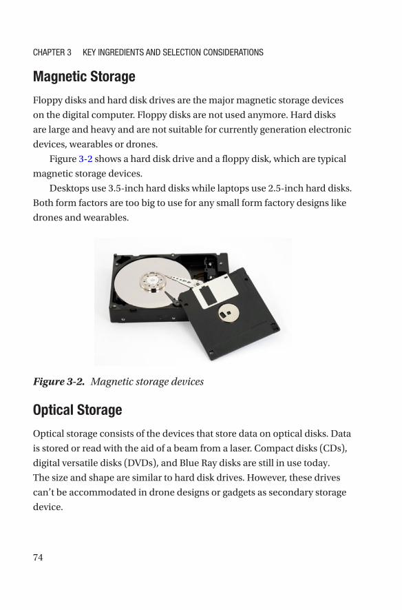
74
Magnetic Storage
Floppy disks and hard disk drives are the major magnetic storage devices
on the digital computer. Floppy disks are not used anymore. Hard disks
are large and heavy and are not suitable for currently generation electronic
devices, wearables or drones.
Figure 3-2 shows a hard disk drive and a floppy disk, which are typical
magnetic storage devices.
Desktops use 3.5-inch hard disks while laptops use 2.5-inch hard disks.
Both form factors are too big to use for any small form factory designs like
drones and wearables.
Optical Storage
Optical storage consists of the devices that store data on optical disks. Data
is stored or read with the aid of a beam from a laser. Compact disks (CDs),
digital versatile disks (DVDs), and Blue Ray disks are still in use today.
The size and shape are similar to hard disk drives. However, these drives
can’t be accommodated in drone designs or gadgets as secondary storage
device.
Figure 3-2. Magnetic storage devices
Chapter 3 Key IngredIents and seleCtIon ConsIderatIons
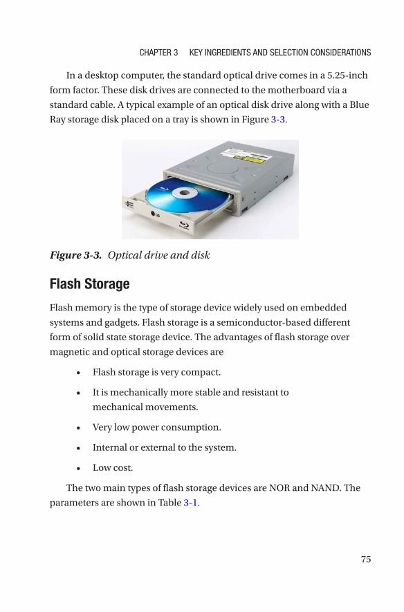
75
In a desktop computer, the standard optical drive comes in a 5.25-inch
form factor. These disk drives are connected to the motherboard via a
standard cable. A typical example of an optical disk drive along with a Blue
Ray storage disk placed on a tray is shown in Figure 3-3.
Flash Storage
Flash memory is the type of storage device widely used on embedded
systems and gadgets. Flash storage is a semiconductor-based different
form of solid state storage device. The advantages of flash storage over
magnetic and optical storage devices are
• Flash storage is very compact.
• It is mechanically more stable and resistant to
mechanical movements.
• Very low power consumption.
• Internal or external to the system.
• Low cost.
The two main types of flash storage devices are NOR and NAND. The
parameters are shown in Table 3-1.
Figure 3-3. Optical drive and disk
Chapter 3 Key IngredIents and seleCtIon ConsIderatIons

76
Both NAND and NOR flash devices are used as secondary memories
in systems in different forms of solid state storage. They can be either
internal, a device soldered on the board, or external through a JEDEC
standard connector.
CompactFlash
CompactFlash is a popular external memory used in cameras and other
handheld devices that need large storage. Based on the Parallel Advanced
Technology Attached interface, CF cards measure 43.8mm by 36.4mm and
are available with storage capacities ranging up to 512 GB. Though this is
smaller than a magnetic device, it’s still too big for a consumer drone.
CompactFlash cards need 3.3V or 5V for operation. CompactFlash
memory is usually an external storage device. A standard CompactFlash
connector is present on the system where the flash device will be plugged
in. Figure 3-4 shows a typical compact storage device.
Table 3-1. NOR vs. NAND Flash
Parameter NOR NAND
read speed Fast slow
Write speed slow Fast
erase time Fast slow
addressing Memory mapped address By row and column address
direct read yes no
error detection and
correction
no yes
application program/mass storage program
Chapter 3 Key IngredIents and seleCtIon ConsIderatIons
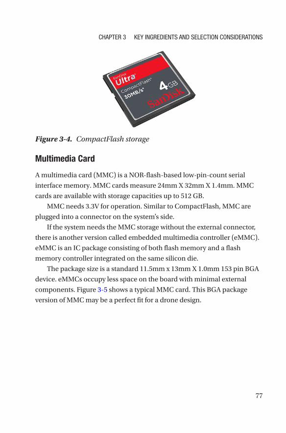
77
Multimedia Card
A multimedia card (MMC) is a NOR-flash-based low-pin-count serial
interface memory. MMC cards measure 24mm X 32mm X 1.4mm. MMC
cards are available with storage capacities up to 512 GB.
MMC needs 3.3V for operation. Similar to CompactFlash, MMC are
plugged into a connector on the system’s side.
If the system needs the MMC storage without the external connector,
there is another version called embedded multimedia controller (eMMC).
eMMC is an IC package consisting of both flash memory and a flash
memory controller integrated on the same silicon die.
The package size is a standard 11.5mm x 13mm X 1.0mm 153 pin BGA
device. eMMCs occupy less space on the board with minimal external
components. Figure 3-5 shows a typical MMC card. This BGA package
version of MMC may be a perfect fit for a drone design.
Figure 3-4. CompactFlash storage
Chapter 3 Key IngredIents and seleCtIon ConsIderatIons

78
Secure Digital Card
Secure Digital (SD) is another NAND flash-based low-pin-count serial
interface memory, similar to a MMC card but with improvements. There
are different versions of SD cards available in various speeds and voltage
levels.
Unlike CompactFlash and MMC, SD cards support different sizes:
standard, mini, and micro. These three physical sizes make the SD card a
more convenient choice for most current generation systems.
• Standard size:
• SD (SDSC), SDHC, SDXC, SDIO
• 32.0x24.0x2.1mm
• 32.0x24.0x1.4mm
• Mini size:
• SD, SDHC, SDIO
• 21.5x20.0x1.4mm
Figure 3-5. MMC/SD card
Chapter 3 Key IngredIents and seleCtIon ConsIderatIons

79
• Micro size:
• SD, SDHC, SDXC
• 15.0x11.0x1.0mm
Figure 3-6 shows a typical micro SD card. It may be the perfect fit for
the drone’s external expandable storage.
Solid State Drives
Flash-based SSDs are storage devices that primarily use electronics
interfaces compatible with traditional block input/output hard disk drives.
The SSD form factor is the same as that of a traditional hard disk drive.
Unlike hard disk drives, SSDs have no mechanical components. SSDs
are more resistant to physical shocks than other flash storage devices. SSD
uses NAND flash technology.
There is other version of SSD available: micro SSD. It can be soldered
on the board with the interfaces directly connecting to the SOC instead of
using a bulky connector. This device package is also small and best suited
for a smaller form factor design like drones. However, it’s an expensive
solution compared to all other storage technologies.
Figure 3-7 shows a typical example of a SSD drive. This is a connector-
based SSD solution with a form factor similar to a SATA hard drive.
Figure 3-6. Micro SD card
Chapter 3 Key IngredIents and seleCtIon ConsIderatIons
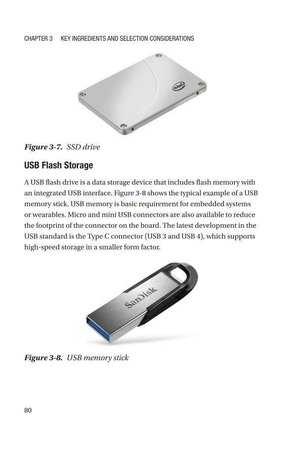
80
USB Flash Storage
A USB flash drive is a data storage device that includes flash memory with
an integrated USB interface. Figure 3-8 shows the typical example of a USB
memory stick. USB memory is basic requirement for embedded systems
or wearables. Micro and mini USB connectors are also available to reduce
the footprint of the connector on the board. The latest development in the
USB standard is the Type C connector (USB 3 and USB 4), which supports
high-speed storage in a smaller form factor.
Figure 3-7. SSD drive
Figure 3-8. USB memory stick
Chapter 3 Key IngredIents and seleCtIon ConsIderatIons

81
Key ConsiderationsA drone system will always be exposed to mechanical stresses like
vibrations, free fall, and drops. It is better to avoid storage devices with
mechanical parts. This clearly eliminates the mechanical and optical
storage devices as secondary storage devices for drones. Also, drone
designs should avoid storage devices with connectors. Storage devices
soldered down on the board are ideal.
Which means, the integrated eMMC and uSSD devices are the most
suitable for drones. The storage capacity of eMMC and uSSD are limited.
The current technology doesn’t support capacity beyond 256GB per
device. Terabyte eMMC and uSSD may be available in the future. For uSSD,
a standard SATA interface is required from the host side, which offers lower
pin count compared to the eMMC and SD card interfaces.
The micro SD card (SDXC) format can go up to terabytes, which also
occupies less space on the board with a higher pin count compared to uSSD.
Considering all the parameters, uSSD looks to be a better solution,
though it is expensive than the others. The higher the capacity, the higher
the price for any flash device.
Generally, no system depends on a single storage device. The same
rule applies for drones. If the space is available, providing additional
backup storage devices is necessary. If uSSD serves as the principal
integrated memory, SD card and USB flash devices can serve as external
extended storage devices. The system has to accommodate SD card and
USB connectors to enable the backup storage. These storage devices can
be plugged into the system when required.
The following is the list of key parameters to be checked before
selecting a storage device:
• Storage capacity
• Size
• Cost
Chapter 3 Key IngredIents and seleCtIon ConsIderatIons
82
• Host interface
• Operating voltage
• Security features like encryption and authentication
SolutionsMicro SSD is perfect for very small factor devices like drones and other
embedded systems. The micro SSD BGA package combines a SATA
flash controller with the latest in small geometry SLC NAND flash,
multiple power supplies, and security features including encryption,
authentication, RNG, anti-tamper, and a self-destruct feature in a single
device. For illustration purpose, the device selected for the drone has the
following features:
• Host accessible capacity up to 128GB
• Integrated switching power supplies with a single
power supply 3.3V
• Footprint replaceable with 256GB and higher-capacity
devices
• Zero power standby
• 524-pin BGA package of 32mm X 28mm
In addition to the micro SSD part, a micro SD card connector or a
USB connector can be provided on the system for the external detachable
storage devices. There can be multiple storage solutions for any systems
for backup if the PCB has the available space to accommodate these
devices. The storage solution for the drone is shown in Figure 3-9.
Chapter 3 Key IngredIents and seleCtIon ConsIderatIons

83
Communication ModuleThe communication module is the device capable of transmitting
analog or digital signals over a wired or wireless communication
channel. The module interfaces with the host processor through any of
the standard interfaces like UART, SDIO, or PCIe. The digital data from
the host processors is converted to a protocol suitable for modulation/
demodulation and then transmitted through wireless protocols. There are
different categories of wireless networks, based on the speed, distance,
and data rate requirements of the system. The higher the performance, the
higher the implementation cost of the wireless networks.
Figure 3-9. Storage solution for the drone
Chapter 3 Key IngredIents and seleCtIon ConsIderatIons

84
CategoriesWiFi, Bluetooth, 3G/4G mobile communication, and RF communications
are the different communication technologies used for data and control
communications. The system will have one or all of these wireless
networks based on the requirements. Each technology is unique in
implementation and operation and follows a different standard.
Whenever a system adds wireless communication, there will be
intentional and unintentional radiation added to the system. The system
needs to be strictly compliant to any regulatory standards so that it does
not cause any interference with any other communication internal or
external to the device. More details on regulatory and certification issues in
upcoming chapters.
Generally, any electronic system needs to be certified by an
international regulatory organization based on the class of equipment.
This is more stringent for systems that use wireless radios.
WiFi+BT
With current technologies, advanced WiFi and Bluetooth communication
technologies are integrated. These compact short-range modules are fully
certified with integrated antennas and software stacks that can interface
with the SOC with a simple UART interface. There are some more advanced
modules available with the PCIe interface to achieve a very high data rate.
These modules can be placed on the board (PCB antenna) and expose
the integrated antenna without any external antenna by covering it with
nonmetallic mechanical parts. These modules are available in different
form factors and are easy to integrate and plug-and-play with the host
processor. Pre-certified M.2, MiniPCIe, and LGA module packages are a
few of the standard packaging available.
All the WiFi devices are based on the IEEE 802.11 standard. Wi-Fi
is a trademark of the Wi-Fi Alliance, which restricts the use of the term
“Wi-Fi Certified” to products that successfully complete interoperability
Chapter 3 Key IngredIents and seleCtIon ConsIderatIons

85
certification testing. Figure 3-10 shows an M.2 form factor WiFi+BT
module that can be plugged into the drone system. The connector for this
module is part of the primary motherboard of the drone.
Mobile Network
Adding a mobile network to the drone provides many advantages. Mobile
connectivity primarily helps the drone for command and control. This
also improves safety because all the real-time information from the drone
can be sent over the network to the drone traffic management. A mobile
network on the drone also helps control drone beyond the line of sight,
provided the area has enough network coverage.
The different types of mobile networks that can be added to the drone
are 3G, 4G (LTE), or the current 5G network. Similar to the WiFi+BT
module, precertified cellular modems are available from different wireless
companies. These modems are available in different categories for
different bands corresponding to different regions.
Long-Term Evolution (LTE) is the current high-speed mobile network
used extensively. LTE is a high-speed wireless communication based on its
predecessors, the GSM/EDGE and UMTS/HSPA technologies. It increases
the capacity and speed using a different radio interface together with core
network improvements. LTE devices are based on the 3GPP standard.
Figure 3-10. Integrated WIFI+BT module in a M.2 form factor
Chapter 3 Key IngredIents and seleCtIon ConsIderatIons

86
IR/RF Wireless
Many drones, embedded systems, wearables, and appliances have IR or RF
remote controls. These days, commercial, off-the-shelf RF transmitters and
receivers are available for drones. The off-the-shelf transmitter-receiver
combination can be used to control the drones remotely and to stream
video and audio remotely. Miniature modules are available with the latest
technology and can be directly integrated with the system.
Several 2.4 GHz precertified solutions are readily available. Modern
2.4GHz RF protocols have higher bandwidth data rates and can allow
audio and video streams independent of control links.
Key ConsiderationsA wireless connection is mandatory to control the drone remotely. There
are different ways of implementing the control links and data links for the
drone system. In a crop monitoring drone, there can be a single solution
for control and data communication or there can be two dedicated
channels for control and data communication.
The coverage area for a wireless LAN and a mobile network is limited,
so the drone needs a RF communication channel for a control link to cover
longer distances.
RF remote control can be the dedicated control path, and WiFi+BT
or mobile network can be the dedicated data path. Considering that the
drone needs to live stream the data or access the cloud for analysis at
regular intervals, either the wireless LAN or the mobile network will serve
the purpose.
WiFi+BT is a better solution than a mobile network in terms of cost,
power consumption, and design complexity. Live streaming of data is
not possible if the drone is not in the network coverage area. The drone
needs to process the data offline or fly to the coverage area to upload data.
Another way is to add more WiFi access points near the drone’s fly zone.
Chapter 3 Key IngredIents and seleCtIon ConsIderatIons

87
SolutionThe wireless solutions for drones vary in technology, size, and cost. The
basic features of the WiFi+BT solution of Intel-based module are shown in
Figure 3-11 and listed below. The solution is the designer’s choice based
on the application of the drone.
The WiFi module selected is the M.2 form factor pluggable precertified
module. The features of the module are as follows:
• Dual-band wireless AC: 2.4 GHz, 5 GHz
• TX/RX streams: 1X1
• Max speed: 433 Mbps
• WiFi Certified: 802.11ac
• Bluetooth version: 4.2
Figure 3-11. Drone communication solution
Chapter 3 Key IngredIents and seleCtIon ConsIderatIons
88
• Size: 22mm X 30mm X 2.4mm
• Host interface: PCIe, USB
• Form factor: M.2 2230, 1216
CameraCameras play a significant role in systems that offer imaging as a primary
function. These days, it’s very difficult to find electronics systems or
gadgets without cameras. The camera serves as an eye for the machines.
A camera for our system is the integration of discrete components
such as image sensors, an image sensing processor, and power modules.
Electrical interconnects and software are the other necessary items for the
camera.
The sensor is the heart of the camera, and it can be either CMOS- or
CCD-based. There are millions of photodetector sites sensitive to the
visible spectrum called pixels.
A normal imaging color camera replicates the human eye and can
cover all the colors of the visible spectrum. A spectral imaging camera
can cover beyond the visible spectrum including ultra violet and infrared
regions. Such cameras capture all of the spectrum during daylight. During
the absence of sunlight, the target objects should be illuminated with
high temperature (around 3000K) halogen lamps to capture the infrared
spectrum.
CategoriesEvery digital camera sensor works by capturing light in an array of photo
sites. When the exposure begins, each side is uncovered by shutters to
collect the incoming light. When the shutter closes, the exposure ends
and the content of each photo site is read as an electrical signal, which is
Chapter 3 Key IngredIents and seleCtIon ConsIderatIons

89
stored as a numerical value in an image file. The stored values measure the
quantity of light.
The camera module usually supports the USB 2, MIPI, and LVDS
interfaces. The latest and most advanced camera modules support the
USB 3.1 host interface. This makes system integration easier with the module.
Monochrome
Monochrome sensors capture all of the incoming light at each pixel,
regardless of color. Each pixel captures 3x more light, since red, green,
and blue are absorbed. Monochrome sensors are able to capture higher
resolution images.
Color
Color sensors capture only one of the three primary colors at each photo
site in an alternating pattern, using something called a color filter array.
The most successful is the Bayer Pattern, which uses alternating rows of
red-green and green-blue filters.
Unlike with monochrome, each pixel effectively captures 1/3 of the
incoming light, since any color not matching the pattern is filtered out.
Any red or blue light that hits a green pixel won’t be recorded.
Spectral Imaging
Spectral imaging, also known as hyperspectral imaging, provides a digital
image with far more spectral information for each pixel than traditional
color images. The raw capture has a stack of tens to hundreds of pictures
with each successive image representing its own specific color, or
equivalently, as a detailed spectral curve for each pixel.
Chapter 3 Key IngredIents and seleCtIon ConsIderatIons

90
Key ConsiderationsFor a crop monitoring drone, a simple monochrome or color cameras
will not suffice. The camera has to go beyond the color wavelengths to
capture the anatomy of leaves, stem, pods, flowers, and fruits. For example,
to monitor leaf health and nutrition value, the camera has to capture the
internal chlorophyll pattern and distribution, which is beyond the visible
spectrum and includes the IR and UV region.
The system can have multiple cameras to cover the intended spectrum.
The system can combine a primary hyperspectral camera and additional
monochrome or color cameras to improve the accuracy of the system.
In a drone system, the camera module needs to be placed externally or
protrude on the bottom with rotatable plate, so that it covers 360-degree
field of view. These modules can be off the shelf or custom-made as per
the system requirement.
The power source and host interface can be through the external UBS
3.0 cable from the module to the system or through a separate power cable
in addition to the USB 3.0 data cable.
SolutionsA single hyperspectral imaging camera is mandatory for a crop monitoring
drone. There can be other cameras like a flight view or a first person view
camera for a better user control experience. Users can observe the flight
path in a display attached to the remote control.
The imaging solution for our hyperspectral crop monitoring drone is
shown in Figure 3-12.
Chapter 3 Key IngredIents and seleCtIon ConsIderatIons

91
The features of the hyperspectral imaging camera module are as
follows:
• Sensor: Hyperspectral imaging
• Type: Line scan
• Spectral range: 600-970
Figure 3-12. Drone imaging solution
Chapter 3 Key IngredIents and seleCtIon ConsIderatIons

92
• Bands: 100+
• Host interface: USB 3.0
A hyperspectral imaging sensor can generate a RGB color image
aligned with spectral images with multiple bands. The sensor can capture
all the required wavelengths during daylight under the bright sunlight.
During low light conditions, the camera works better if accompanied
with a halogen flash. A halogen lamp can generate the required
temperature when flashed on the objects. This creates the required
infrared wavelengths from the light reflections from the object along with
the RGB color image.
DisplayThe current generation systems have different sizes of integrated displays.
A display is required for any system that runs an operating system. A
display is helpful during the installation of the operating system, drivers,
and other software.
CategoriesFrom the system design perspective, there are two kinds of displays
available. Displays can be either built-in (internal) within the system or
external.
Internal
Internal displays are commonly used in laptops, tablets, and mobile
phones. An internal display makes the device more portable and reduces
the dependencies from external displays for development, operation,
debugging, and troubleshooting of the system. Since they must be built
into a system that is already small, the display must be smaller with less
Chapter 3 Key IngredIents and seleCtIon ConsIderatIons

93
resolution. Smaller displays can offer an integrated touch screen, which is
a more convenient input device these days.
Internal displays are powered using internally generated power from
the system. The backlight used for the display will be the most power-
consuming subsystem.
Generally, the host interface used in internal displays is LVDS, MIPI, or
eDP. The displays either integrate the controller inside or externally. Even
if there is no compatible interface in the SOC, there are options available to
convert any display, interface, and protocol to make it compatible for the
display.
External
External displays are standard computer monitors available in various
sizes and a wide range of resolutions. These displays are powered
externally and connect to the system either by a standard AV cable, a VGA
cable, a DVI cable, or HDMI cable.
External displays are more suitable for the system, which doesn’t need
a monitor all the time. It’s only required when there is a system upgrade,
installation, development, debugging, or any other activity. However, a
display is not mandatory for any embedded system.
Key ConsiderationsA display is not mandatory for the drone system. An external display
connector can be added as a backup display. An optional display can
be added on the remote controller to get a first person view of the drone
during the flight. This gives a better user experience for the operators.
An external display can be any of the low profile display connectors
like micro HDMI, mini DP, or Type C. This will help check and analyze the
images from the drone directly by connecting a monitor externally when
the drone is not in flight.
Chapter 3 Key IngredIents and seleCtIon ConsIderatIons

94
An optional integrated display can be attached to the remote
controller. A dedicated video transfer communication channel is required
between the drone and the remote to live stream the video.
Flight ControllersThe flight controller is the most important subsystem in a drone. A flight
controller receives commands from the user and controls the propellers
and motors to keep the drone in flight. It also receives other commands
like image capture, video capture, and any other use case commands from
the user and executes them while the drone is in the air.
CategoriesThere are different types of off-the-shelf flight controllers readily available
specifically for drones. They are available in different form factors and
varying sizes.
MCU/MPU
Microcontroller/microprocessor-based flight controllers are available
in different form factors. They are plug-and-play and can be integrated
with the system with less effort. The performance of the controllers
and the accuracy of the sensors will vary with the cost. Obviously, high
performance flight controllers are more expensive.
FPGA
Other than microcontrollers and microprocessors, there are FPGA or
custom-made ASIC-based high performance flight controllers available.
They are the most expensive solutions that integrate additional capability.
A system that doesn’t need an off-the-shelf flight controller can have an
on-board FPGA with on-board sensors.
Chapter 3 Key IngredIents and seleCtIon ConsIderatIons

95
Key ConsiderationsKey considerations for a flight controller are the complexity of integration
with the system, supported sensors, flying capability, and cost. Most
advanced flight controllers are easy to install and integrate with the host
computer.
SolutionsThe features of any flight controller are listed as follows in the product brief
or in the datasheet:
• 32-bit microcontroller/ARM cortex processor/FPGA
• Gyroscope and accelerometers
• Barometer
• Magnetometer
• GPS
• Supports quadcopter, hexcopter, tricopter, and
octocopter
BatteryDrones are supposed to fly high, so they must carry their own power
supply. Drones are powered using fuel, solar, or batteries. For industrial
drones used in the agriculture field, the battery is the main source of
the power. The battery is recharged when the drone is not in use or is
stationed.
Chapter 3 Key IngredIents and seleCtIon ConsIderatIons

96
CategoriesMost electronics gadgets and drones these days use rechargeable batteries.
The most common rechargeable batteries are covered in the following
sections.
Lead Acid
Lead acid is the oldest rechargeable battery system. Lead acid is rugged,
forgiving if abused, and economically priced. But it has a low specific
energy and limited cycle count. Lead acid is used for wheelchairs, golf
cars, personnel carriers, emergency lighting, and uninterruptible power
supplies.
Nickel Cadmium
Mature and well understood, NiCd is used where long service life, high
discharge current, and extreme temperatures are required. NiCd is one of
the most rugged and enduring batteries; it is the only chemistry that allows
ultra-fast charging with minimal stress. Its main applications are power
tools, medical devices, aviation, and UPS. Due to environmental concerns,
NiCd is being replaced with other chemistries, but it retains its status in
aircrafts due to its good safety record.
Nickel Metal Hydride
NiMH serves as a replacement for NiCd as it has only mild toxic metals and
provides higher specific energy. NiMH is used for medical instruments,
hybrid cars, and industrial applications. NiMH is also available in AA and
AAA cells for consumer use.
Chapter 3 Key IngredIents and seleCtIon ConsIderatIons
97
Lithium-Ion Batteries
Li-ion is taking over many applications that were previously served by
lead and nickel-based batteries. Due to safety concerns, Li-ion needs a
protection circuit. It is more expensive than most other batteries, but its
high cycle count and low maintenance reduce the cost per cycle over many
other chemistries.
Lithium batteries are the most suitable batteries in electronic gadgets
and especially in drones based on the following features and advantages:
• Characteristics: Small dry cell batteries, sealed,
rechargeable
• Form factor: Custom sizes in plastic cases, small
cylinders, button cells
• Applications: Cell phones, laptops, power tools, hybrid
automobiles, video cameras, handheld electronics,
drones
• Safety: Non-spillable, non-toxic
Key ConsiderationsThe first step in any battery selection is calculating the max current
consumption of the drone system. System power consumption varies
based on the KPIs. Maximum power is drawn during the max KPI, which
drains the battery at a faster rate.
For example, if the drone power consumption is 10A during the video
recording in flight, a 10000mA battery will last for an hour.
The nominal voltage of the battery is based on the battery architecture.
If a single cell of a lithium ion battery can generate nominal 3.7V, 10A, two
such cells in parallel will generate same voltage with twice the current, so
20A. Two such cells in series will generate twice the amount of voltage 7.2
Chapter 3 Key IngredIents and seleCtIon ConsIderatIons

98
with 10A of current. So for a drone, the cell architecture should be two cells
in a series, which is also called 2S1P architecture, which means two cells in
series and one parallel.
There is another parameter called charge rate on the datasheet.
Usually the charger design is based on the standard charging rate.
However, some systems need fast charging to reduce the charging time of
the system. In that case, the charger design should be done in such a way
as to charge the batteries at the faster rates.
SolutionsBattery specifications are generally listed in the vendor datasheets and are
as follows:
• Nominal capacity: 10000mAh
• Nominal voltage: 7.2V
• Voltage at end of discharge: 5.6V
• Charging voltage: 8.56V
• Standard charge: 0.2C CC/CV
• Standard discharge: 0.2C CC/CV
• Fast charge: 0.5C CC/CV
• Fast discharge: 0.5C CC
• Maximum continuous charge current: 5000mA
• Maximum continuous discharge current: 5000mA
• Product dimension: Length x width x thickness in mm
Chapter 3 Key IngredIents and seleCtIon ConsIderatIons

99
Thermal SolutionA common problem in product design, particularly in electronics, is
managing the thermal conditions for optimal efficiency. The core of the
challenge is designing energy-efficient microprocessors and printed circuit
boards that will not overheat.
A frequently overlooked aspect of thermal management problem
solving is architectural design. Whether it’s a private home, an office
building, or a dedicated server room or drone, architectural considerations
can have a huge impact on the thermal management solutions available.
CategoriesTo tackle and alleviate the difficulties and inefficiencies that arise as a
result of heat, engineers employ different cooling systems to manage
conditions. These systems can be divided into two main categories: those
with active and those with passive cooling techniques.
Active Cooling
Active cooling refers to cooling technologies that rely on an external device
to enhance heat transfer. Through active cooling technologies, the rate of
fluid flow increases during convection, which dramatically increases the
rate of heat removal.
Active cooling solutions include forced air through a fan or blower,
forced liquid, and thermoelectric coolers (TECs), which can be used to
optimize thermal management on all levels. Fans are used when natural
convection is insufficient to remove heat. They are commonly integrated
into electronics, such as computer cases, or are attached to CPUs, hard
drives, or chipsets to maintain thermal conditions and reduce failure risk.
Chapter 3 Key IngredIents and seleCtIon ConsIderatIons

100
The main disadvantage of active thermal management is that it
requires the use of electricity and therefore results in higher costs
compared to passive cooling.
Passive Cooling
The advantages of passive cooling techniques lie in the energy efficiency
and lower financial cost, making it an astute system design choice for the
thermal management of both buildings and electronic products.
Passive cooling achieves high levels of natural convection and heat
dissipation by utilizing a heat spreader or a heat sink to maximize the
radiation and convection heat transfer modes. In architectural design,
natural resources like wind or soil are used as heat sinks to absorb or
dissipate heat. This leads to proper cooling of electronic products and
thermal comfort in homes or office buildings by keeping them under the
maximum allowed operating temperature. A growing trend in this regard
can be witnessed in what is commonly known in the industry as passive
houses.
Passive thermal management is a cost-effective and energy-efficient
solution that relies on heat sinks, heat spreaders, heat pipes, or thermal
interface materials to maintain optimal operating temperatures.
Key ConsiderationsLike other electronic gadgets, the boards on drones do need cooling
solutions. There are significant advantages and disadvantages of both
active and passive cooling systems. There is no restriction on using active
or passive. Table 3-2 shows the list of key features to be checked before
finalizing a solution.
Chapter 3 Key IngredIents and seleCtIon ConsIderatIons

101
SolutionsFor a drone design, the weight and size of the solution is a high priority. An
active cooling solution is the right choice.
Power dissipation is managed by a section of low power fans. Since the
drone will be flying to perform the intended application and producing
enough noise with the propellers of the quadcopter, noise from the board
doesn’t make any difference.
A better cooling solution can be provided with active cooling system
on a drone system design.
InterconnectsAn interconnect is an electrical or optical connection or cable that
connects two devices or more. An interconnect joins electric conductors
electrically and mechanically to other conductors and to the terminals of
Table 3-2. Active vs. Passive Cooling
Key Features Active Passive
Weight low high
Compact size yes no
noise yes no
power dissipation high low
performance degradation no yes
operation cost high low
orientation yes no
reliability no high
eco-friendliness no yes
Chapter 3 Key IngredIents and seleCtIon ConsIderatIons

102
electrical devices. Interconnects are passive electrical components that
contain two terminals that store energy in their magnetic field, such as a
cable connecting a hard drive or a monitor connecting to a computer. A PC
contains several interconnects.
Since a drone is a complex electromechanical system, choosing the
right interconnects is critical to achieve the best performance.
CategoriesThere are wide range of interconnect parts from several manufacturers
that can be used onboard to connect electrical parts and subsystems.
Electronic cable connectors, board-to-board connectors, electrical wire-
to-board connectors, RF connectors, and FPC/FFC connectors are the
most frequently used connectors for electrical connections on board.
Cable Connectors
USB
The USB connection is quite possibly the most pervasive connection
type in today’s world. Nearly every form of computer peripheral device
like keyboards, mice, headsets, flash drives, and wireless adapters can be
connected to your computer through a USB port. The design has evolved
over the years, which means there are multiple versions of USB available:
• USB 1.0/1.1 can transmit data at speeds up to 12 Mbps.
• USB 2.0 can transmit data at speeds up to 480 Mbps
and is compatible with older versions of USB. At the
time of this article, USB 2.0 is the most common type
found in the market.
• USB 3.0 can transmit data at speeds up to 4.8 Gbps. It is
compatible with previous versions of USB.
Chapter 3 Key IngredIents and seleCtIon ConsIderatIons

103
The mini and micro USB variants are most often used with smaller,
portable devices like PDAs, phones, and digital cameras. The standard USB
connectors are more often used on devices that tend to remain plugged in,
like external hard drives, keyboards, and mice.
Ethernet
Ethernet cables are used to set up local area networks. In most cases,
they’re used to connect routers to modems and computers. If you’ve ever
tried to install or fix a home router, you’ve likely dealt with an Ethernet
computer cable. Nowadays, they come in three varieties:
• Cat 5 cables are the most basic type and provide speeds
of either 10 Mbps or 100 Mbps.
• Cat 5e, which means Cat 5 Enhanced, allows for faster
data transmission than its predecessor. It caps at 1,000
Mbps.
• Cat 6 is the latest and offers the best performance of the
three. It’s capable of supporting 10 Gbps speeds.
Other than USB and Ethernet, there are different standard cables and
cable connectors are available. These cables are categorized into power,
data, display, analog, digital, RF cables. VGA, HDMI and DVI are examples
for display cables. USB, Ethernet Copper and Ethernet Fiber are examples
for data cables.
Board-to-Board Connectors
Board-to-board connectors are used to connect printed circuit boards
(PCBs), an electronic component that contains a conductive pattern
printed on the surface of the insulating base in an accurate and repeatable
manner. Each terminal on a BTB connector is connected to a PCB. A BTB
connector includes housing and a specific number of terminals.
Chapter 3 Key IngredIents and seleCtIon ConsIderatIons

104
Three different mounting types of board-to-board connectors are
through hole, surface mount, and press fit technology. Two primary PCBs
can be sandwiched or connected right angle with there connectors.
BTB connectors are selected by considering the mounting method, pin
pitch, number of rows (a.k.a. number of ways), pin length, stacker height,
etc.
Wire-to-Board Connectors
This type of device connects a wire to a printed circuit board (PCB),
enabling connectivity between circuits. Manufactured for flexibility and
reliability, wire-to-board connectors are engineered for low-profile mating
and secure terminations, with products equipped with either a friction
lock mechanism or a full lock mechanism. Multiple or single connection-
type PCB tabs include stud mount, printed circuit mount, wire crimp,
testing, weld, and adapters for quick disconnect applications.
Complex electromechanical system like drone may use many wire to
board connectors across the system. For Example, the 360 degree view
camera at the bottom of the drone may need a special cabling, which may
not entangled when camera covers 360 degree. This should be flexible
enough not to obstruct the camera view and allowing the camera to do a
full rotation keeping the electrical contact stable.
RF Connectors
A coaxial RF connector (radio frequency connector) is an electrical
connector designed to work at radio frequencies in the multi-megahertz
range. RF connectors are typically used with coaxial cables and are
designed to maintain the shielding that the coaxial design offers. Better
models also minimize the change in transmission line impedance at the
connection. Mechanically, they may provide a fastening mechanism
(thread, bayonet, braces, blind mate) and springs for a low ohmic electric
Chapter 3 Key IngredIents and seleCtIon ConsIderatIons

105
contact while sparing the gold surface, thus allowing very high mating
cycles and reducing the insertion force. Research activity in the area
of radio-frequency (RF) circuit design has surged in the 2000s in direct
response to the enormous market demand for inexpensive, high-data-rate
wireless transceivers.
FPC/FFC Connectors
FPC/FFC is a one-piece connector that makes the connection with a
directly-inserted FFC or FPC and locks it by means of a lever. This type of
connector can be used in a wide range of digital devices when a low profile
or the horizontal insertion of flex is required.
Key ConsiderationsGenerally speaking, electrical connectors are mechanical components
that serve an electrical function. In addition to carrying electrical current
at a specified voltage, connectors either enable interconnection of
components during the assembly process or enable the user to easily
disconnect and reconnect different parts of the equipment. The size and
shape of connectors varies based upon the electrical requirements of the
equipment, the physical space within the equipment, and environmental
conditions in which the equipment must operate.
Connector manufacturers typically catalog connectors based upon
interconnections, which refer to the connector application or mechanical
method of interconnection. These applications range from connecting the
chip to a circuit board to connecting peripherals to devices and beyond.
Connectors that are attached to or mated with a printed circuit board
comprise a large majority of catalog connector offerings.
Chapter 3 Key IngredIents and seleCtIon ConsIderatIons

106
Connectors are selected based on the following requirements:
• Application environment
• Electrical requirements
• Mechanical requirements
• Safety and regulatory requirements
SolutionsThe selection of connectors is strictly based on the applications and the
board form factor. There are multiple interconnects required for the board
and the system.
MechanicalsAs discussed, several mechanical items must be added to complete the
drone system. The key mechanical items are the quadcopter, propellers,
enclosures, and mechanical interconnects. The quadcopter is the key
component that decides the skeleton of the drone. Apart from these key
mechanical components, there are numerous mechanicals inside the
drone enclosures including the PCBA.
CategoriesIn any system design, the mechanical items are categorized into make or
buy items. The quadcopter, plastic enclosures, and other customer parts
inside the drone will be designed with the mechanical CAD tool in-house
by the mechanical engineers. They are custom-made parts specific to the
Crop monitoring drone.
Chapter 3 Key IngredIents and seleCtIon ConsIderatIons
107
Once the design is complete in the CAD tool, the files are shared with
the manufacturers to prepare for the material and to manufacture the final
component.
The other category is the buy items. Propellers, fans, landing
gears, screws, and washers are usually buy items, and they can be
purchased from the vendors directly by providing them requirements or
specifications.
Key ConsiderationsThe key considerations for selecting a quadcopter and the respective
enclosure is as per the target dimensions, target weight, and other
mechanical factors like board, camera module dimensions, and weight.
For example, selecting a simple quadcopter has so many advantages over
other multicopter designs:
• It’s a simple design and the frame is easily available on
the market for easy integration.
• They are less expensive than other multicopters.
• They are suitable for all kinds of flight functions like
roll, pitch, yaw, and motion.
• The quadcopter can be done either with an X-frame or
H-frame.
If there are readily less expensive quadcopters available in the market,
this can be a buy item instead of make item. This reduces the effort and
cost further for the drone makers.
Similarly, the enclosures and other mechanical components like
landing gears, screws, and washers are selected based on the needs and
included in the BOM for procurement as buy item. The only mechanical
component that is very complicated and requires an expert’s suggestion
before purchase is the propellers.
Chapter 3 Key IngredIents and seleCtIon ConsIderatIons

108
Many commercially available motors and propellers are available for a
drone. The key considerations are
• Lift: The drone should be able to provide two times the
amount of thrust than the weight of the quadcopter.
This includes the weight of the board and other
mechanical components inside the drone.
• Size: The proper ratio of motor size to frame size.
• Power: The higher the voltage, the higher the speed of
the motor. This means more power is necessary. There
needs to be proper tradeoff between these features
when selecting a propeller.
• Specs: Other specs of the motor like RPM, thrust, no
load, and efficiency play a key role in the selection.
SolutionsConsider all the specs to pick the appropriate propellers for this drone.
The camera can be fit on the bottom side of the drone to give a proper
360-degree view. An enclosure will cover all the parts of the drone except
the propellers on the top and the camera on the bottom. The plastic
enclosures will also cover the daughterboard on the top side and expose
the antennas for better reachability.
SummaryIn this chapter, you scanned through the ingredients selection and key
considerations with a few examples of drone-specific ingredients. The
process and procedure is same for any small component adding into the
design at any stage. It is always the designer’s responsibility to check the
Chapter 3 Key IngredIents and seleCtIon ConsIderatIons

109
feasibility and select the best component from the different options. Apart
from design considerations, the components must comply with industrial
standards for industrial drones. And a general rule is that all components
should be RoHS-compliant, which is restriction of hazardous substances
on the component or in the manufacturing process of the component. This
applicable for drone manufacturing also.
Chapter 3 Key IngredIents and seleCtIon ConsIderatIons

111© Neeraj Kumar Singh, Porselvan Muthukrishnan, Satyanarayana Sanpini 2019 N. K. Singh et al., Industrial System Engineering for Drones, https://doi.org/10.1007/978-1-4842-3534-8_4
CHAPTER 4
Drone Hardware DevelopmentIn the previous chapter, you explored the key considerations for few of
the essential ingredients of a drone. This chapter will explain how the
electrical ingredients are put together to develop the hardware for the
drone. At a high level, drone development can split into drone hardware
development and drone system development. Drone hardware or PCBA
development is a critical part of system development. The design or
selection of components other than hardware completes the system
design.
In any electronics system, the PCBA is considered as one single
assembly item, particularly in a drone system, where the mechanical
and electrical components play an equal and important role. Even then,
hardware is the only item that goes through a complicated design process.
Unlike the PCBA, other system-level ingredients are either easily procured
or manufactured from dedicated suppliers.
PCBA development starts with the architecture, followed by
the electrical ingredients selection, which was discussed in the
previous chapters. The architecture and ingredients selections are the
documentation part of the hardware development. The actual design
requires electrical CAD tool involvement most of the time. The PCBA
design process has several steps, which can go in parallel or sequential.

112
The first step of the design is PCBA library development and the final step
is getting a complete, functionally working PCBA. To get the final working
PCBA, the total development cycle is split into design and validation cycles.
As mentioned earlier, this completed PCBA will be a single mechanical
component assembled in a drone system.
PCB Library DevelopmentPCB library development is the important task of PCB design and is a time-
consuming task. It’s usually done by highly trained professionals in all
aspects of library management from creating library elements through to a
complete library management environment. A library is usually managed
in a central server or a cloud, which provides access to the components for
several boards or projects at the same time.
Libraries are created in a specific file format and stored as individual
files. Different tools use different file formats. Libraries created for
a specific tool can’t be interchanged with other tools. The electrical
component library is a one-time creation process and will stay in the
server forever. Each component created or newly added will have unique
part identification in the same component library.
The entire library has to comply with the latest design technologies as
well as standards such as IPC-7351B to ensure a high-quality library.
Symbol CreationLibrary development is nothing but symbol creation for the required
electrical components in the system. Two types of symbols are created by
any board developers in hardware design. They are logical or schematics
symbols and CAD symbols or PCB footprints.
A logical symbol is the visual representation of an electrical ingredient
in the schematics. Similarly, a footprint is the visual representation of an
electrical ingredient in a PCB layout.
Chapter 4 Drone harDware Development

113
Schematics are the visual representation of an electrical circuit. The
completed schematic has all of the required symbols connected to each
other with wires (nets) as per the design requirement.
The PCB layout is the visual representation of the actual PCB with all
of the required PCB footprints connected to each other with copper traces
in a multilayer PCB. The PCB layout is done with dimensions and scales
matching the actual PCB and finally fabricated to a physical PCB.
Each individual component in the schematic has an individual
logical symbol. One or more logical symbols can use same footprint, if the
components share the same package. For example, the logical symbol for
resistors is the same for all of the values. The designer has to pick the right
value for their design. New resistor values are added to the same logical
symbol and are maintained as component libraries whereas complex
integrated circuits use unique logical symbols for each component.
Technical specifications are added for each component along with other
attributes like manufacturer part number and manufacturer name. The
footprint is usually added as an attribute for the logical symbol.
Logical Symbol Creation
Every electrical CAD design software/project has a separate librarian
tool to create, verify, and manage the component libraries. All symbols
are created in a simple 2D plane with simple drawing tools like squares,
rectangles, and circles. Discrete components such as resistors, capacitors,
inductors, and diodes are created with their unique 2D representation with
pins, which is commonly seen in text books. ICs are created as a square or
rectangle box with pins attached to it.
A standard practice is to create the symbols with grids. Having grids in
the symbols makes the schematic drawing easy; the schematic also should
follow a similar grids. Symbols can be created in different styles. Generally,
there are guidelines and BKMs (best known methods) to standardize the
symbols and schematics for the whole organization.
Chapter 4 Drone harDware Development

114
Pin names and numbers typically match with the names and numbers
from the component datasheet or the device collaterals. A few examples
of logical symbols used in a drone power circuit are shown in Figure 4-1.
Clockwise from the left corner is a resistor, capacitor, power, ground,
inductor, and IC. All of the components shown in the architecture block
diagram in Figure 2-2 have a corresponding logical symbol and footprint
with all the associated discrete components.
Figure 4-1. Logical symbol examples
Symbol Verification
Symbol verification is an important process associated with symbol
creation. Once the symbol is created, it needs to be verified by the
requested/concerned design engineer before adding it into the central
library.
Chapter 4 Drone harDware Development
115
The created symbol should meet the standards and BKMs, and more
importantly the symbol should be well-suited for the schematic design.
The pins are arranged in such a way that the connections can be done
with other peripheral components in a presentable manner and better
readability.
So it is crucial to verify that the symbol is created as per the
requirement. A symbol cannot be modified once it is added to the central
library, which enables other board developers to use the same symbol for
other boards and different projects.
PCB Footprint Creation
Similar to logical symbol creation, PCB footprint creation is done with a
2D electrical CAD tool with a simple drawing window. Unlike the logical
symbol creation, footprint creation requires a different expertise. A
footprint is the exact representation of component pads or a land pattern
with proper scale. All footprints are also provided with component height
information to generate a 3D view from a layout file if needed.
The footprint is the exact replica of the component pads including
dimensions, unlike the logical symbol, which is the only visual
representation of the component in a schematic.
A footprint is the visual representation of the component in a PCB
layout. The fabricated bare PCB will have all the component pads, exactly
created as a footprint on which the components are mounted. This bare
PCB with all the components mounted completes the hardware and
provides a finished PCBA.
Figure 4-2 shows a completed layout with all the component
footprints. Footprints are red for resistors, purple for capacitors, yellow for
inductors, and green for IC. Every block in the drone architecture block
diagram in Figure 2-2 has a PCB footprint with an associated discrete
component.
Chapter 4 Drone harDware Development

116
Footprint Verification
Footprint verification is also a critical process, similar to the logical symbol
verification. Generally, there are multiple levels of verification done to
check the footprint compliance with the IPC guidelines. The footprint
is added in the library and accessed by board developers through the
component libraries.
Schematics DesignSchematics design is the representation of the detailed electrical circuit
elements interconnection within a system. Schematics give a detailed view
of the components and the connections between them. It’s the precise
low-level design of the hardware block diagram shown in the Figure 4-3.
Figure 4-2. PCB footprint examples
Chapter 4 Drone harDware Development

117
Every electrical component of the system is placed on the schematic
and connected with other components logically and functionally as per
the design. Schematics are done considering all the electrical rules, laws,
and guidelines for proper operation. Generally, schematic designs are
produced by professional analog and deigital electronics design engineers.
Schematics CaptureThe drone architecture diagram in Figure 2-2 is converted to a multiple
page electrical circuit in a schematics capture. A simple hardware circuit
with fewer components can be accommodated on a single page. A complex
hardware circuit like a drone can’t be done on a single page. Multiple pages
show multiple components connected across the pages. Connections
across the pages are always presented with off-page connectors.
All the connections are labelled with net names for easy identification
on the layout. Connections without net names are provided with random
names and numbers when generating net list. This helps engineers
identify and understand the electrical connection and types on a layout
tool after importing the schematics files in a layout.
Connections are usually divided into power, ground, and signals.
Signals are classified as analog, digital, and RF signals. Digital signals are
further classified as high speed and low speed signals. Each connection
or interface follows the set of electrical guidelines for connections and
terminations. These signal terminations are represented in schematics
with appropriate components like resistors, inductors, and capacitors on
the actual connection.
In a schematic, each component is provided with a unique reference
designator. This reference designator helps to identify the particular
component throughout the hardware development especially in layout,
bill of materials, testing, and validation.
Chapter 4 Drone harDware Development

118
In addition to the component datasheet, every component
manufacturer provides a recommended design. This recommended
design is based on the evaluation board design and tested data from the
manufacturer. However, a designer can choose to design a completely new
circuit that is different from the reference circuit. An example schematic of
a power component is shown in Figure 4-3.
There are numerous complicated circuit designs for the complete
drone hardware, interconnected to each other on multi-page schematics,
which may or may not follow the reference circuit from the datasheet.
Figure 4-3. Schematics example
Design Rules CheckingDesign Rules Checking (DRC) is a powerful automated feature that checks
both the logical and physical integrity of a design. Checks are made against
any or all enabled design rules embedded in the tool. The tool generates
reports and suggestions.
This feature should be used on every schematic to show that electrical
rules have been maintained and to ensure there are no other design
violations. It is particularly recommended that a design rule check always
be performed prior to generating the final netlist.
Chapter 4 Drone harDware Development

119
There are also tools available for circuit simulation. Simulation allows
the designer to check the circuit operation. However, simulation requires
the actual electrical model of the components or the schematic needs to be
exported to other simulation tools with all of the electrical specifications of
the component.
Generating a NetlistNetlist generation is the final step in the schematic design. In electronic
design, a netlist is a description of the connectivity of an electronic circuit.
In its simplest form, a netlist consists of a list of the electronic components
in a circuit and a list of the nodes they are connected to. A network (net) is
a collection of two or more interconnected components.
The structure, complexity, and representation of a netlist can vary
considerably, but the fundamental purpose of every netlist is to convey
connectivity information. Netlists usually provide nothing more than
instances, nodes, and perhaps some attributes of the components
involved.
For the Crop monitoring drone, three different schematics and netlists
are generated. One is for the main board, one for the daughterboard, and
one for the flex PCB board.
Bill of MaterialsThe bill of materials (BOM) is a key data set generated from a board design
project either from a schematic or a layout tool. This report-type document
provides a listing of all components required to build the product,
including the bare board, which is essentially the base “component” upon
which all other parts are assembled. The BOM acts as a guide for what
needs to be procured to build the product as designed. It also provides a
means to calculate the cost based on the required number of assembled
Chapter 4 Drone harDware Development

120
boards in a requested spin. The BOM is generated through a dedicated and
powerful report generation engine, the interface of which is known as the
Report Manager from the tool itself.
An electrical BOM can be in a spreadsheet format with attributes in
each column. Attributes are usually provided for each component while
creating the logical symbol.
The schematics entry tool provides the options to generate the BOM in
multiple formats.
Since creating a schematic is a manual, time-consuming process, a
BOM is generated frequently from the partially completed schematics.
This partial BOM is called an intermediate demand BOM, and it’s sent
to the PCBA manufacturing factory. The factory communicates to the
suppliers and requests the components and required quantities.
Early submission of the demand BOM is better for long lead
components. This enables the supplier to get the required quantities from
their side to meet the PCBA manufacturing schedule. Figure 4-4 shows an
example of a tool-generated BOM.
For the drone design, three different electrical BOMs are generated for
the motherboard, daughterboard, and flex PCB.
Figure 4-4. Tool-generated BOM
Chapter 4 Drone harDware Development

121
Symbol AttributesThere are certain inputs to be taken care in a schematics tool to generate a
BOM. The key inputs are symbol attributes. General BKM is to provide all
the symbol attributes while creating a logical symbol itself. Figure 4- 5
shows the symbol attribute window from a schematics tool. The first
column shows the attribute names, and the corresponding symbol
attributes are provided in the second column. A complete, clean BOM can
be generated from the schematic if the logical symbol is provided with all
the required properties in a BOM.
Figure 4-5. Symbol attribute window
Chapter 4 Drone harDware Development

122
BOM GenerationA BOM can be generated from the project source documents or from the
active PCB document using the Reports > Bill of Materials command from
the schematic or PCB editor.
The tool-generated BOM is shared with the PCBA manufacturer to
add additional information required for the BOM, usually local supplier
and cost data. Being able to cost a project and determine the quantities
of design components to be ordered from suppliers/distributors is an
essential part of the overall design process.
The following supplier-based data can be included in a bill of materials
by the factory. Designers can also add this data into the tool-generated
BOM itself, if they have access to all this information from suppliers or
factory.
• Supplier: Name of the supplier
• Supplier currency: Alphabetic code for the chosen
currency used for pricing data. Usually US dollars for
most suppliers.
• Supplier order quantity: Number of units required to
fulfill the desired production quantity of the product.
• Supplier part number: Part number for the supplier
item. This is different from the manufacturing part
number.
• Supplier stock: How many units of the item the supplier
has in stock.
• Supplier subtotal: The supplier order quantity
multiplied by the supplier unit price, resulting in the
subtotal for that item.
• Supplier unit price: Cost per unit of the supplier item.
Chapter 4 Drone harDware Development

123
Material ReadinessKeeping the materials ready for the PCBA is a complicated process in any
factory. Each component needs to be checked frequently and followed up
with the supplier for stock. Once the design is fixed for one particular part
number, it cannot be modified after fabricating the board.
There may be some footprint-compatible components available from
the same vendor or competitive vendor. But getting the stock at the right
time is difficult and so is meeting the schedule.
Layout DesignThe completed schematic circuit of the design is transformed into a
PCB. The netlist from the schematic is imported into the layout tool as the
base. The electrical components need to be grouped and placed in order to
comply with all the electrical guidelines when routing the signals.
The PCB layout can be performed manually (using CAD) or in
combination with an auto route. The best results are usually still achieved
using at least some manual routing, simply because the design engineer
has a far better judgement of how to arrange circuitry. Many auto-routed
boards are often completely illogical in their track routing; the program has
optimized the connections and sacrificed any small amount of order that
may have been put in place by manual routing.
The CAD PCB layout consists of several layers; for illustration, often the
layers are colored and compressed into the one overlay image. The circuit
design and the PCB overlay image are usually supplied by the designer
to the client in a PDF document produced by the CAD package. The PCB
overlay may quite easily be printed in the actual size, cut out, and used
for approximate size comparisons with mechanical items. For instance,
the print can be placed inside the actual enclosure to see how it will be
positioned in relation to other parts. Components can also be placed up
against the pad markings as a quick idiot-check of dimensions.
Chapter 4 Drone harDware Development

124
The width of the tracks is a trade-off based on current flow, space
available, size of parts, and electromagnetic interference. The track layout
is a similar trade-off that also picks when to dodge from one side of the
board to the other to avoid an obstacle, but overall normally aims to
find the shortest regular path between the connected points. Given the
impedance, susceptibility, and signal on tracks, the loop area is another
trade-off that is considered as the design proceeds. Added to all this is the
design for manufacture.
Board OutlineFor a drone, one possible shape is a rectangular board, considering the
mechanical structure. But it’s not uncommon to see round, triangular, or
other interesting PCB shapes. Drone PCBs are designed to be as small as
possible, but that’s not necessary if your application doesn’t require it.
If you are putting the PCB into a drone enclosure, the dimensions may
be limited by the size of the housing. In that case, you need to know the
enclosure’s dimensions before laying out the PCB so that everything fits
inside. As seen in the second chapter, the ID defines the size of the PCB
and outline.
The various components also have an effect on the size of the finished
PCB. For instance, surface-mounted components are small and have
a low profile, so you’ll be able to make the PCB smaller. Through hole
components are larger, but they’re often easier to find and solder.
Layer Stack-UpLarger circuits can be difficult to design on a single- or double-layer
PCB. Most of the component packages are BGA packages, which need
signals to be routed in an internal layer. Considering the density of the
signals and complexity of the routing, you might need multiple layers
with different layer vias to achieve the smallest size. A first-level initial
Chapter 4 Drone harDware Development

125
assessment is done during the architecture phase, as seen in Chapter 2,
and is carried forward to the actual layout design, with modifications if
required.
Most PCB manufacturers let you order different layer thicknesses.
“Copper weight” is the term manufacturers use to describe the layer
thickness, and it’s measured in ounces. The thickness of a layer will affect
how much current can flow through the circuit without damaging the
traces. Trace width is another factor that affects how much current can
safely flow through the circuit. To determine safe values for width and
thickness, you need to know the amperage that will flow through the trace
in question. An online trace width calculator can help determine the ideal
trace thickness and width for a given amperage.
Generally, multiple layer PCBs have few continuous ground layers
where the entire layer is covered with a copper plane connected to ground.
The positive traces are routed on top and connections to ground are made
with through holes or vias. Ground layers are good for circuits that are
prone to interference because the large area of copper acts as a shield
against electromagnetic fields. They also help dissipate the heat generated
by the components.
Electrical ConstraintsIn a professionally designed PCB, most of the copper traces bend at 45°
angles. One reason for this is that 45° angles shorten the electrical path
between components compared to 90° angles. Another reason is that
high-speed logic signals can get reflected off the back of the angle, causing
interference.
This drone project uses digital logic or high-speed communication
protocols above 200 MHz. All general high-speed guidelines are
applicable, like avoiding 90° angles and vias in the traces. For slower speed
circuits, 90° traces won’t have much of an effect on the performance of
your circuit.
Chapter 4 Drone harDware Development

126
Like layer thickness, the width of your traces will affect how much
current can flow through your circuit without damaging the circuit.
The proximity of traces to components and adjacent traces will also
determine how wide your traces can be. When designing a small PCB with
lots of traces and components, you might need to make the traces narrow
for everything to fit.
Signal Integrity
The challenges of high-speed design require some additional effort to
ensure signal integrity. This can be achieved by following fundamental
analog design rules and using careful PCB layout techniques.
A transmission line can be defined as a “conductive connection
between a transmitter and a receiver capable of carrying a signal.”
Traditionally, transmission lines are thought of as telecom-based
cables operating over long distances. However, with high-speed digital
signal transmission, even the shortest passive PCB track suffers from
transmission line effects. At low frequencies, a wire or a PCB track may
be considered to be an ideal circuit without resistance, capacitance, or
inductance. But at high frequencies, AC circuit characteristics dominate,
causing impedances, inductances, and capacitances to become prevalent
in the wire.
Impedance Mismatch
Unequal impedance of the source output, line, receiver, or load causes
impedance mismatch. This mismatch means the transmitted signal is not
fully absorbed within the receiver and the excess energy is reflected back to
the transmitter. This process continues back and forth until all of the energy
is absorbed. At high data rates, this can cause signal overshoot, undershoot,
ringing, and stair-step waveforms, which produce signal errors. Impedance
mismatch can be overcome by matching the transceiver buffers to the
Chapter 4 Drone harDware Development
127
transmission media. In the case of a PCB, this can be achieved by careful
selection of the medium and by the use of termination schemes.
The termination scheme used to overcome impedance mismatch
depends on the application. The schemes include simple parallel
termination and more complex RC termination where a resistor capacitor
network provides a low pass filter to remove low frequency effects but
passes the high frequency signal.
Signal Attenuation
High-frequency signal transmission line losses make it difficult for the
receiver to interpret the information correctly. The following two types of
transmission line losses are due to the transmission medium:
• Dielectric absorption: High-frequency signals excite
molecules in the insulator, which cause the insulator
to absorb signal energy. This absorption reduces the
signal strength. Dielectric absorption relates to the
PCB material and can be lessened by careful material
selection.
• Skin effect: Varying current waveforms caused by
AC and high-frequency signals tend to travel on the
conductor’s surface. Signals traveling on the surface
cause the self-inductance of the material to produce
an increased inductive reactance at high frequencies,
which forces electrons to the material’s surface. The
effective reduction of the conductive area causes an
increase of resistance and, therefore, attenuation of
the signal. Increasing track width can reduce the skin
effect, but this is not always possible.
Chapter 4 Drone harDware Development

128
Cross Talk
Whenever a signal is driven along a wire, a magnetic field develops around
the wire. If two wires are placed adjacent to each other, it is possible
that the two magnetic fields interact, causing a cross-coupling of energy
between signals known as crosstalk. The following two energy coupling
types are the predominant causes of crosstalk:
• Mutual inductance: A magnetic field causes induced
current from the driven wire to appear on the quiet
wire. This mutual inductance causes positive waves to
appear near the transmitter end of the quiet line (near
end inductance) and negative waves at the receiver end
of the transmission line (far end crosstalk).
• Mutual capacitance: The coupling of two electric fields
when current is injected in the quiet line proportional
to the rate of change of voltage in the driver. This
mutual capacitance causes positive waves near both
ends of the transmission line.
Power Integrity
Power integrity (PI) is an analysis to check whether the desired voltage and
current requirements are met from source to destination. Today, power
integrity plays a major role in the success and failure of new electronic
products. There are several coupled aspects of PI: on the chip, on the chip
package, on the circuit board, and in the system. Four main issues must be
resolved to ensure power integrity at the printed circuit board level:
• Keep the voltage ripple at the chips pads lower than the
specification.
• Control ground bounce (also called synchronous
switching noise, simultaneous switching noise, or
simultaneous switching output).
Chapter 4 Drone harDware Development

129
• Control electromagnetic interference and maintain
electromagnetic compatibility: the power distribution
network is generally the largest set of conductors on
the circuit board and therefore the largest antenna for
emission and reception of noise.
• Maintaining a proper DC voltage level at the load at
high currents is challenging. A modern processor or
field-programmable gate array can draw 1-100 Amps at
sub-1V VDD levels with AC and DC margins in the tens
of millivolts. Very little DC voltage drop can thus be
tolerated on the power distribution network.
The current path from the power supply through the PCB and IC
package to the die is called the power distribution network. Its role is to
transfer the power to the consumers with little DC voltage drop and to
allow little ripple induced by dynamic current at the consumer. The DC
drop occurs if there is too much resistance in the plane or power traces
leading from the VR to the load. This can be countered by raising the
voltage on the VR or extending the “sense” point of the VR to the consumer.
Dynamic current occurs when the consumer switches its transistors,
typically triggered by a clock. This dynamic current can be considerably
larger than the static current (internal leakage) of the consumer. This
fast current consumption can pull the voltage of the rail down, creating a
voltage ripple. This change in current happens much faster than the VRM
can react. The switching current must therefore be handled by decoupling
capacitors.
The noise or voltage ripple must be handled differently depending
on the frequency of operation. The highest frequencies must be handled
on-die. This noise is decoupled by parasitic coupling on the die and
capacitive coupling between metal layers. Frequencies above 50-100 MHz
must be handled on the package; this is done by on-package capacitors.
Frequencies below 100 MHz are handled on the PCB by plane capacitance
Chapter 4 Drone harDware Development

130
and using decoupling capacitors. Capacitors work on different frequencies
depending on their type, capacitance, and physical size. It is therefore
necessary to utilize multiple capacitors of different sizes to ensure low
PDN impedance across the frequency range. The physical size of the
capacitors affects its parasitic inductance. The parasitic inductance
creates impedance spikes at certain frequencies. Smaller capacitors are
therefore better. The placement of the capacitors is of varying importance
depending on the frequency of operation. The smallest value capacitors
should be as close as possible to the consumer to minimize the AC current
loop area. Larger capacitors in the micro Farad range can be placed more
or less anywhere.
The target impedance is the impedance at which the ripple created
by the dynamic current of the specific consumer is within the specified
range. In addition to the target impedance, it is important to know which
frequencies it applies, and at which frequency the consumer package is
responsible (this is specified in the datasheet of the specific consumer IC).
Mechanical ConstraintsOne of the more challenging parts of managing today’s electronic product
development process is collaboration among various players of a project.
PCB designers often find themselves negotiating between industrial
or mechanical designers and electrical designers. Requirements from
each team may conflict, and often the PCB designer must resolve these
differences.
The most important step for a mechanical designer and a PCB
designer is to agree on the ground rules for working together. Establishing
a common coordinate system, orientation, dimensioning, and units are
key to getting off to a good start.
Chapter 4 Drone harDware Development

131
Compared to mechanical CAD programs, PCB design software has
very limited mechanical design capabilities:
• Most PCB design software can only view a board in a
single orientation and from a single direction. Boards
are viewed from a single side, and opposite side
features and components are viewed as an “X-ray”
through the board.
• PCB design software typically has much less flexible
dimensioning capabilities. In particular, most PCB
software lacks the automatic linked-in dimensioning
that mechanical CAD users take for granted.
• Most PCB design software has less flexibility in
measuring and documenting distances between
features. Even the lowest-cost mechanical CAD
software implements extensive relative measurements
and features “snap to” capabilities.
Coordinate System
In the circuit board industry, it is standard to place the origin at the lower
left-hand corner of the circuit board, with the horizontal axis as the X
axis and the vertical axis as the Y axis. Some designers prefer to use the
lower left mounting or tooling hole as the origin. For boards with cutouts
or chamfers in that corner, place the origin where the corner would have
been without the cutout or at either remaining corner. For circular or
radially-symmetrical boards, place the origin at the center of the board.
Establishing a useful origin for unusual shaped boards may call for some
creativity.
Chapter 4 Drone harDware Development

132
Orientation
If practical, orient the longest axis horizontally to allow the largest view
area on a standard landscape computer monitor. Create all board drawings
from the same viewpoint, unless there are compelling reasons to show
them in another orientation. If drawings need to be viewed from the
reverse “mirrored” side, be sure to keep the same origin and provide notes
to help the designer definitively establish which edge is which.
Dimension
PCB designers are used to working with coordinate dimensions. Writing
all dimensions in ordinate style removes a common source of error by
eliminating the need to do math to figure out feature and component
locations.
Keep Out Zones (KOZ)
The mechanical designer needs to communicate the following to the PCB
designer:
• Board physical description: Shape of the board,
including slots, cutouts, and thickness, location and
diameter of mounting and tooling holes.
• Design constraints: Maximum component height for
both sides and keep-out areas.
• Location and part numbers of critical components,
especially connectors: Except for the simplest of boards,
this is a lot of information to place in a single drawing.
Cluttered drawings can be difficult to make and
error-prone to read. When in doubt, create separate
drawings for different information. Be sure to keep the
orientation consistent and unambiguous!
Chapter 4 Drone harDware Development

133
Physical Constraints
Draw the shape of the board to scale and detail slots, cut-outs, chamfers,
mounting/tooling holes, and hole clearances. For curved sections, show
the center point and radius, plus the location of the curve end-points.
PCBs are milled to shape so concave corners need to be rounded. If there
are board dimensions that can be expanded or shrunk, indicate them on
the drawing. Be sure to note the required board thickness (0.062”, 0.093”,
and 0.031” thicknesses are few common thicknesses). Creating a system-
level drawing can be a great way to communicate physical constraints.
Show the board superimposed on an enclosure or in relation to other
boards in a system.
Design Constraints
Indicate design constraints such as whether parts may be placed on both
sides and the maximum component heights for each side. Show areas that
need to be free of components or free of traces. Place an arrow and a note
on the drawing to indicate the direction of system airflow.
Component Location
Specifying component locations can be one of the more challenging parts
of a PCB design project. The geometric center is the best reference point
for many parts such as chip resistors, capacitors, diodes, transistors, and
ICs. However, other components such as connectors don’t always have
obvious points of reference. Here are some guidelines:
• Use the geometric center of the mating surface as the
reference point for vertical mount connectors.
• For right-angle connectors, dimension the center line
and front edge.
Chapter 4 Drone harDware Development

134
• For through-hole connectors, include a set of reference
dimensions for at least one pin (pin 1). Note that using
the pad as a reference point does not always work
for surface mount parts as the pad center may not
correspond to either the pin or lead center.
• For all connectors, show the relative position of both
pin 1 and pin 2.
• For FFC/FPC (flat flex cable/flat printed circuit)
connectors, indicate the cable conductive side and
cable plug-in direction. In general, don’t be anxious
about including additional “reference” dimensions.
When in doubt, add a note explaining the chosen
reference points.
It is important to set up the board outline, stack-up, electrical,
and mechanical constraints before importing the netlist. All of these
constraints are general and a few might be more relevant to the drone
design.
NetlistThe netlist is the final output file from the schematic and is also a primary
input for a PCB layout.
The instances, nodes, and attributes of the components involved and
the connections are imported into the layout tool. Once the components
are imported, they can be either placed manually or automatically.
Placement
Components are grouped together based on the functionality and placed
closer to each other to reduce the length of the signal routing.
Chapter 4 Drone harDware Development

135
Figure 4-6 shows an IC highlighted in blue placed inside the board
outline. Associated components highlighted in green for that IC are
grouped together outside the board before being placed inside the board
outline. Other components (in grey) imported from the netlist are already
grouped and placed inside the board outline.
Figure 4-6. A PCB CAD file with partially completed placement
Routing
Once the placement is done, placement review is done by the electrical
designers to check the placement as per the electrical guidelines. CAD
engineers start routing the signals after placement completion. Routing
is done layer by layer, interface by interface. Electrical properties of the
signals are provided in the constraint manager based on the type of the
signal. Different routing is required for different signal types. The trace
width and max length of the signal vary based on the layers used.
Chapter 4 Drone harDware Development
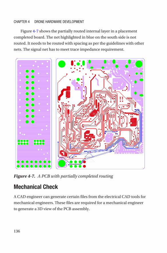
136
Figure 4-7 shows the partially routed internal layer in a placement
completed board. The net highlighted in blue on the south side is not
routed. It needs to be routed with spacing as per the guidelines with other
nets. The signal net has to meet trace impedance requirement.
Figure 4-7. A PCB with partially completed routing
Mechanical Check
A CAD engineer can generate certain files from the electrical CAD tools for
mechanical engineers. These files are required for a mechanical engineer
to generate a 3D view of the PCB assembly.
Chapter 4 Drone harDware Development
137
This 3D view of the PCB assembly is in certain standard file format,
which can be imported to any mechanical tool to check the mechanical
assembly of the drone with other mechanical components already
imported to the tool or designed in the same tool.
Gerber Release
Initially developed by a company with the name of Gerber, the Gerber
format currently refers to a widely accepted standard capable of describing
board images such as conductor layers, solder mask layers, and legend
layers.
Printed circuit boards are designed in a specialized EDA (electronic
design automation) or a CAD system that further generates board
manufacturing data, based on which circuit board fabrications are
commenced. PCB manufacturers won’t fully understand all details of
a PCB design file unless a Gerber format file is generated for reference
and guidelines. The Gerber format file is applied to describe the design
requirement of each image of a circuit board and it can be applied for both
bare board fabrication and PCB assembly.
No one needs a delayed printed circuit board project. Delayed PCBs
often end in huge penalties paid to the manufacture for the wasted
slots. The ideal circumstance is that you send your design file to the PCB
manufacturer, and the manufacturer arranges board fabrication based on
your file and delivers the products to you. The practical situation, however,
is not that simple.
It usually takes a long period of time from the moment you send your
design file out to the final arrival of the boards. Certain effectiveness
and efficiency measures can spare you from unwanted delays in PCB
manufacturing.
When it comes to bare board fabrication, the Gerber format is
called for by both standard photo plotters and other manufacturing
equipment desiring image data like legend printers, direct imagers, or
Chapter 4 Drone harDware Development
138
AOI (automated/automatic optical inspection) equipment. Put simply,
Gerber format files are essential from the beginning to the end of the PCB
fabrication process.
When it comes to PCB assembly, a stencil layer is included in the
Gerber format and component locations are regulated as well, which are
regarded as significant reference data for SMT (surface mount technology)
assembly, thru-hole assembly, and mix of them.
Gerber files do play a crucial role as a connector and translator
between PCB design engineers and PCB manufacturers, enabling
design engineers’ considerations and concepts to be understood by
manufacturers so that correct and reliable products can be effectively and
efficiently manufactured.
SummaryIn this chapter, we discussed general and drone-specific hardware
development procedures and processes. The hardware development cycle
starts with the architecture block diagram, but the actual detailed design
starts from the library creation and schematic design for the multiple
boards in the system. Completed schematics are transferred to the layout
tool with appropriate inputs and prerequisites. The prerequisites for the
layout define the outline, stack-up, and the electrical and mechanical
constraints. Finally, the Gerber release for all the boards required for the
drone marks the end of the drone hardware design cycle, which is the half
mile crossed for the entire development cycle.
Chapter 4 Drone harDware Development

139© Neeraj Kumar Singh, Porselvan Muthukrishnan, Satyanarayana Sanpini 2019 N. K. Singh et al., Industrial System Engineering for Drones, https://doi.org/10.1007/978-1-4842-3534-8_5
CHAPTER 5
System Assembly, Bring-Up and ValidationThe second half of the product development cycle is the board bring-up,
which aids the final system bring-up. No physical hardware or system
parts are seen until the Gerber release. That is when the bring-up, the
actual hardware, and mechanical parts are available for hands-on. The
upcoming chapters will discuss more about the manufacturing, power
on, testing, and validation of the actual hardware and the system. The
pilot system build starts once the system is tested and validated against
all the design and certification requirements as per the PRD. The system
is deployed with the features list. Pilot systems are usually distributed to
internal customers and are restricted to a lab environment until the system
passes the regulatory and precompliance testing. Feedback and input from
customers are consolidated to fine-tune the system further. Often, there is
a separate tool for bug assignment, tracking, and issue resolution.
Regulatory and environmental compliance testing is required
for any electronic product. The presence of wireless radios and other
communication modules on the system makes it mandatory to pass
more stringent compliance standards. Apart from the usual commercial

140
and industrial electronic product certifications, flying an unmanned
aerial vehicle (drone) means compliance with additional standards and
regulations specified by the Federal Aviation Authority (FAA).
This chapter covers the manufacturing and assembly of the drone with
the list of make and buy items ordered as per the system BOM. PCBs are
the primary make item; they are designed in-house and manufactured by
the PCB vendors using a complex manufacturing and assembly process.
PCB Fabrication ProcessFor most of the electronics system design, the PCB manufacturing,
assembly, and bring-up process is the same. The PCB manufacturing
process starts immediately after releasing the Gerber files to the PCB
fabricator. Design engineers will clear any engineering questions raised
by the manufacturer after the initial assessment of the Gerber files. The
fabrication process starts after clearing all the engineering questions. The
design and layout engineers are not involved in the PCB fabrication, but
it is always good to have working knowledge of the process and design for
manufacturing (DFM) concepts. Knowledge of these concepts will improve
the quality of the deliverables in forthcoming PCB designs; this will also
avoid repetitive mistakes and reduce the number of engineering questions.
Fabrication StepsPCB manufacturing companies have specific manufacturing processes
depending on the technologies used by the PCB vendor. In a multilayer
PCB, layers of copper foil, prepreg, and core material are sandwiched
together, as shown in the layer stack-up in Chapter 2. The multiple layers
are pressed together under high temperature and pressure. High pressure
and temperature will melt the prepreg adhesive that holds the multiple
layers into a single PCB.
Chapter 5 SyStem aSSembly, bring-Up and Validation

141
The standard manufacturing steps for a simple double-layer PCB are
as follows:
1. Cut the PCB raw materials to a suitable size and
shape.
2. Drill the PCB for mounting holes and vias as per the
drill file (part of the design package).
3. Plate the drilled holes with copper (thickness as
specified by the design engineers).
4. Press the board with dry film.
5. Transfer the routing to the board by exposing the
dry film and route film on the top. (The routing is
unique for each layer.)
6. Put the board in the electric copper machine to
make the board conductive.
7. Add electric tin to take away the copper protected by
the dry film.
8. Take away the dry film.
9. Use a special liquid to etch the unused copper on
the board.
10. Remove the tin.
11. Apply a solder mask on the board, which is an
epoxy resin and is normally green in color (this
is the material that gives the green color
to the PCB).
12. Expose the solder mask on the component pads for
soldering (top and bottom layer).
13. Print the silk screen.
Chapter 5 SyStem aSSembly, bring-Up and Validation

142
14. Finish the surface.
15. Perform the flying probe test.
16. Run functional and quality checks.
17. Package and ship the bare PCB to the assembly
house.
For a multilayer PCB, the layers are finished individually and pressed
together in the proper sequence with the correct orientation as per the
design file. The multilayer sandwiched board is then electroplated on
the top and bottom layers with the required copper thickness. The board
continues from Step 2 of the PCB process for the top and bottom layers.
The manufacturer can also do a multipack fabrication as per the
designer’s request, if the PCB size is small. A multipack PCBA combines
two or more identical PCBAs, fabricated and assembled in a single PCB
substrate. A multipack can also be done for different PCBAs with the same
layer stack-up. A multipack configuration increases the output and reduces
the cost.
Different types of materials are used for core and prepreg on the
internal layers of a multilayer PCB. The top and bottom layers are usually
thick copper foils electroplated with copper too. The total copper thickness
of the top and bottom layer is the combined thickness of the copper foil
and plating.
The finished thickness of the board is usually +/- 10% from most of
the PCB fabricators. The final board is packed and shipped for the SMT
(surface mount technology) assembly process.
PCB Assembly ProcessUnlike the fabrication, the assembly process needs significant involvement
from the design engineers. As described in previous chapters, the
production BOM (electrical BOM) is the final input for the PCB
Chapter 5 SyStem aSSembly, bring-Up and Validation

143
assembly. The multilayer bare PCB shipped from the fabricator is one of
the line items of the production BOM.
The system BOM can include multiple PCBAs (for example,
motherboard, daughterboard, flex PCBs, etc. in a Crop Squad
drone kind of system). Each PCBA of the system has to go through the
same fabrication and assembly process individually.
PCBA manufacturers also assess the functionality of a PCB design;
this primarily includes a DFM check. This is a preliminary step; the
training and knowledge transfer occurs between the design engineers and
manufacturers before the real PCBA process even begins.
Most companies specializing in PCB assembly need the design file
of the PCB to start out, along with any other design notes and specific
requirements. For more complicated designs, the designers release the
pre-Gerber files as a trial package, before releasing the actual Gerber files,
so that the PCB assembly company can check the PCB file for any issues
that may affect the PCB’s functionality or manufacturability. This activity
captures design for manufacturability issues, short circuits, or any other
electrical problems.
This check also covers the design specifications of a PCB. More
specifically, it looks for any missing, redundant, or potentially problematic
features. Any of these issues may severely and negatively influence the
functionality of the final project. For example, one common PCB design
flaw is leaving too little spacing between PCB components, which can
result in shorts and other malfunctions.
By identifying potential problems through DFM checks before
manufacturing begins, you can cut manufacturing costs and eliminate
unanticipated expenses. This is because these checks cut down on the low-
yield issues.
Boards can be powered on immediately after the assembly. There are
some key steps to be followed to get the board ready for power-on. They
are manual, best known methods, followed traditionally in any PCBA
bring-up process.
Chapter 5 SyStem aSSembly, bring-Up and Validation
144
Surface Mount Assembly ProcessThe surface mount assembly process is the assembly of the surface mount
devices on a PCB. There are a wide range of SMD component packages
available on the market and they come in various shapes and sizes;
for example, BGA, QFN, and LGA are different varieties of SMT
packages offered for an IC.
Surface mount technology was developed to build highly complex
electronic circuits into smaller and smaller assemblies with good
repeatability and with a higher level of automation. SMT reduces the
manufacturing costs and enables the engineers to use the PCB space more
efficiently. There are step-by-step processes necessary to complete an SMT
of a PCB.
Solder Paste Stenciling
Applying a solder paste to the board is the first step of the assembly
process. A thin stainless-steel stencil is placed over the PCB, which
is similar to placing a mask in a screen printing process. This allows
technicians to apply solder paste only to certain pads of the target
PCB. These pads are where components will sit on the finished PCB.
The solder paste is a greyish substance consisting of tiny balls of metal,
also known as solder. The solder paste mixes solder with a flux, which is a
chemical designed help the solder melt and bond to a surface. Solder paste
appears as a grey paste and must be applied to the board at exactly the
right places and in precisely the right amounts.
In a professional PCBA line, which is also called a SMT line, a
mechanical fixture holds the PCB and solder stencil in place. An applicator
places the solder paste on the intended areas in precise amounts. The
machine spreads the paste across the stencil, applying it evenly to every
open area. After removing the stencil, the solder paste remains in the
intended locations or the component pads.
Chapter 5 SyStem aSSembly, bring-Up and Validation

145
Pick and Place
After applying the solder paste to the PCB board, the PCBA process moves
on to the pick-and-place machine, a robotic device that places surface
mount components, or SMDs, on a prepared PCB. SMDs account for most
non-connector components on PCBs today. These SMDs are soldered
onto the surface of the board in the next step of the PCBA process.
Traditionally, this was a manual process done with a pair of tweezers,
in which rework technicians had to pick and place components by hand.
This step is now an automated process among all the PCB manufacturers
these days. This shift occurred largely because machines tend to be more
accurate and more consistent than humans.
The device starts the pick-and-place process by picking up a PCB
board with a vacuum grip and moving it to the pick-and-place station. The
robot orients the PCB at the station and begins applying the SMTs to the
PCB surface. These components are placed on top of the soldering paste in
preprogrammed locations.
Reflow Soldering
Once the solder paste and surface mount components are all in place,
they need to remain there. This means the solder paste needs to solidify,
adhering the components to the board. The PCB assembly accomplishes
this through a process called reflow.
Once the pick-and-place process concludes, the PCB board is
transferred to a conveyor belt. This conveyor belt moves through a large
reflow oven, which is somewhat like a commercial pizza oven. This
oven consists of a series of heaters which gradually heat the board to a
temperature around 250 degrees Celsius, or 480 degrees Fahrenheit. This is
hot enough to melt the solder in the solder paste.
Once the solder melts, the PCB continues to move through the oven. It
passes through a series of cooler heaters, which allow the melted solder to
Chapter 5 SyStem aSSembly, bring-Up and Validation

146
cool and solidify in a controlled manner. This creates a permanent solder
joint to connect the SMDs to the PCB.
Many PCBAs require special consideration during reflow, especially
for a two-sided PCB assembly. A two-sided PCB assembly needs stenciling
and reflowing for each side separately. First, the side with fewer and
smaller parts is stenciled, placed, and reflowed, followed by the other side.
Inspection and Quality Control
Once the surface mount components are soldered in place after the
reflow process, as a next step the assembled board needs to be tested for
functionality. Often, movement during the reflow process will result in
poor connection quality or a complete lack of a connection. Shorts are also
a common side effect of this movement, as misplaced components can
sometimes connect portions of the circuit that should not connect.
Checking for these errors and misalignments can involve one of several
different inspection methods. The most common inspection methods
include manual, automatic, and X-ray check.
Manual Checks
Despite the upcoming development trend of automated and smart
manufacturing, manual checks are still relied upon in the PCB assembly
process. For smaller batches, an in-person visual inspection by a designer
is an effective method to ensure the quality of a PCB after the reflow
process. However, this method becomes increasingly impractical and
inaccurate as the number of inspected boards increases. Looking at such
small components for more than an hour can lead to optical fatigue,
resulting in less accurate inspections.
Chapter 5 SyStem aSSembly, bring-Up and Validation

147
Automatic Checks
Automatic optical inspection is a more appropriate inspection method
for larger batches of PCBAs. An automatic optical inspection machine,
also known as an AOI machine, uses a series of high-powered cameras to
“see” PCBs. These cameras are arranged at different angles to view solder
connections. Different quality solder connections reflect light in different
ways, allowing the AOI to recognize a lower-quality solder. The AOI does
this at a very high speed, allowing it to process a high quantity of PCBs in a
relatively short time.
X-Ray Check
Another method of inspection involves X-rays. This is a less common
inspection method. It’s used most often for more complex or layered PCBs.
The X-ray allows a viewer to see through layers and visualize lower layers
to identify any potentially hidden problems.
After all these checks, the fate of a malfunctioning board depends on
the PCBA company’s standards; they will be sent back to be cleared and
reworked, or scrapped.
Whether an inspection finds one of these mistakes or not, the next step
of the process is to test the part to make sure it does what it’s supposed to
do. This involves testing the PCB connections for quality. Boards requiring
programming or calibration require even more steps to test proper
functionality.
Such inspections can occur regularly after the reflow process to
identify any potential problems. These regular checks can ensure that
errors are found and fixed as soon as possible, which helps both the
manufacturer and the designer save time, labor, and materials.
Chapter 5 SyStem aSSembly, bring-Up and Validation

148
Through Hole Assembly ProcessPCBs with more electrical interconnects and mechanical components
include through hole connectors beyond the usual SMDs. Drone boards
are very good example and have an equal number of SMDs and through
hole components. These can be plated through hole components or non-
plated through hole components.
A plated through hole is a hole in the PCB that is plated all the way
through the board. PCB components use these holes to pass a signal from
one side of the board to the other. In this case, soldering paste will not do
any good, as the paste will run straight through the hole without a chance
to adhere.
Instead of soldering paste, PTH components require a more
specialized kind of soldering method in the later PCB assembly process.
Manual Soldering
Manual through hole insertion is a straightforward process. Typically,
one person at a single station is tasked with inserting one component
into a designated PTH. Once they are finished, the board is transferred
to the next station, where another person works on inserting a different
component. The cycle continues for each PTH that needs to be outfitted.
This can be a lengthy process, depending on how many PTH components
need to be inserted during one cycle of the PCBA. Most companies
specifically try to avoid designing with PTH components for this very
purpose, but PTH components are still common among PCB designs.
Wave Soldering
Wave soldering is the automated version of manual soldering, but involves
a very different process. Once the PTH component is put in place, the
board is put on yet another conveyor belt. This time, the conveyor belt
runs through a specialized oven where a wave of molten solder washes
Chapter 5 SyStem aSSembly, bring-Up and Validation

149
over the bottom of the board. This solders all of the pins on the bottom of
the board at once. This kind of soldering is nearly impossible for double-
sided PCBs, as soldering the entire PCB side would render any delicate
electronic components useless.
After this soldering process is finished, the PCB can move to the final
inspection, or it can run through the previous steps if the PCB needs
additional parts added or another side assembled.
Final Inspection and Functional TestAfter the soldering step of the PCBA process is finished, a final inspection
will test the PCB for its functionality. This inspection is known as a
functional test. The test puts the PCB through its paces, simulating the
normal circumstances in which the PCB will operate. Power and simulated
signals run through the PCB in this test while testers monitor the PCB’s
electrical characteristics.
If any of these characteristics, including voltage, current, or signal
output, show unacceptable fluctuation or hit peaks outside of a
predetermined range, the PCB fails the test. The failed PCB can then be
recycled or scrapped, depending on the company’s standards.
Testing is the final and most important step in the PCB assembly
process since it determines the success or failure of the process. This is also
the reason why regular testing and inspection throughout the assembly
process is so important.
Post ProcessSoldering paste leaves behind some amount of flux, while human handling
can transfer oils and dirt from fingers and clothing to the PCB surface.
Once all is done, the results can look a little unclean, which is both an
aesthetic and a practical issue.
Chapter 5 SyStem aSSembly, bring-Up and Validation

150
After months of remaining on a PCB, flux residue starts to smell and
feel sticky. It also becomes somewhat acidic, which can damage solder
joints over time. Additionally, customer satisfaction tends to suffer when
shipments of new PCBs are covered in residue and fingerprints. For these
reasons, washing the product after finishing all the soldering steps is
important.
A stainless steel, high-pressure washing apparatus using deionized
water is the best tool for removing residue from PCBs. Washing PCBs in
deionized water poses no threat to the device. This is because it’s the ions
in regular water that do damage to a circuit, not the water itself. Deionized
water, therefore, is harmless to PCBs as they undergo a wash cycle.
After washing, a quick drying cycle with compressed air leaves the
finished PCBs ready for power-on.
Typically, the design engineers will be present at the factory to do
the initial power-on. The factory power-on helps the engineers to fix
any assembly-related issues in the factory itself. The skilled staff and the
trained rework technicians can do the reworks at the same quality level as
the machines.
Board Power-OnOnce the PCBA is completed, there are several key preliminary and sanity
checks to be done to ensure the board is ready for power-on. Powering on
the board without finishing these steps can spoil the board, and there’s a
chance that the board can go dead and never become usable. This is why
sanity tests are important; otherwise the efforts of many engineers to get a
PCBA working will be in vain. A board can look like it works, but actually
can have multiple hidden hardware issues that only pop up later when
developing firmware/software, making the issues very difficult to debug.
This is because the many independent subsystems communicate with
each other and work together for complete functionality.
Chapter 5 SyStem aSSembly, bring-Up and Validation

151
There is a large variation of possible things to check. They must be
done very carefully and all observations must be captured so they can be
revisited in case of any issues. The traditional checks before powering on a
PCBA are elaborated below.
Basic InspectionThe first step is to check that all of the components used on the top and
bottom layers are soldered as per BOM. Assembly is strictly as per install or
no-install components in the production BOM.
No-install components are the optional components used in the
design; they’re not required for the power-on or basic functionality. This is
usually for future scaling or backup circuits for secondary features.
All of the components should be verified for the manufacturing part
numbers. Manufacturing part numbers should match exactly as given in
the BOM, including the version ID and date code if any.
The pin 1 marking or orientation should match with the assembly
file or the board file released along with the design package to the PCBA
manufacturer.
Polarity of the discrete components should be verified as per the
design. Installing polarized components like diodes, capacitors, and
inductors in reverse can lead to shorts or component damage.
There should not be any visible short circuits between pads upon
visual inspection. The pads should be soldered with good quality (QFN
pads, connectors with a small pitch). High-end microscopes can
check smaller size components clearly.
Short-Circuit ChecksAfter completing the sanity check, the board has to be verified for
impedance and shorts. All the power rail points should be measured for
impedance with respect to ground and other power rails. There must
Chapter 5 SyStem aSSembly, bring-Up and Validation

152
not be any short (0 ohm resistance) between the power-to-power and
power-to-ground connections.
Some power rails have very low impedance. The CPU core voltage of
the latest generation processors from Intel with multiple cores can even
show 1 ohm impedance due to the high current requirement for that rail.
Some power rails may show low impedances like 20 ohms, 40 ohms, or 90
ohms due to higher current consumption.
Impedance of all the power rails should match the requirement before
power-on. For example, all power rails shown in Figure 2-10 in Chapter 2
should show finite resistance when measured with a digital multimeter,
which qualifies the board for safe power-on.
Power CheckIf all the rail impedance is as expected or calculated, the next step is to
connect the main input power to the board as per the main input power
requirement. If the system is battery powered, it gets connected to a fully
charged battery. Typically, a bench-top power supply with a digital display
(for current and voltage) is used to feed power through the battery
connectors to know the total current consumption of the board. This lets
the test engineer limit the input current to the board to avoid any high
current intake or system damage in case of any short.
The latest generation of SOCs categorize the rails for power and energy
management. The always-on rails must be on at all the time, irrespective
of the power state. A few rails may not be required by default; they will be
available only when the appropriate software/firmware is installed. As a
first step, always-on rails are verified on the board.
For example, in a drone system, the power for the propellers can be
off when system is idle and grounded. It can be switched on when the
system needs to take off when the application starts. This will save some
power and protects the battery from draining. These rails are completely
dependent on the software or application.
Chapter 5 SyStem aSSembly, bring-Up and Validation
153
When the required input power is supplied to the board, the always-on
power supply comes up. These power rail voltages should pass the voltage
level and tolerance criteria as per the requirement.
For other voltages to come up, firmware or software needs to installed,
which is the next step of the bring-up process. Power supplies that don’t
pass the exit criteria may have issues on the actual design, assembly, or
even PCB.
A digital multimeter is suitable equipment to measure the power rails.
Sequencing and Reset CheckPower sequencing is an important feature to be tested, if all the power
rails are as expected and meet the required tolerance. As explained in
the previous chapter, every device needs specific power sequencing. The
overall power sequencing is designed by consolidating all the individual
device power sequencing requirements.
A multiple channel cathode ray oscilloscope (CRO) is the suitable
equipment to check the power sequencing. Latest generation CROs
support four channels simultaneously. Four rails can be connected
together and the timings between those rails can be measured.
A high bandwidth CRO is required to measure the faster ramp timings
and the very minute delays between power signals. Typically, there are
individual enable and rest signals for different devices. All of them are
control signals to be measured along with the power rails. A platform reset
signal is the last signal released at the end of any power sequencing, which
is usually released from the last power device to the SOC, after which the
entire platform comes out of reset.
Figure 2-11 is an example of a power sequencing requirement. The
timings on the actual board can be measured by probing the signals using
a CRO. Capturing any two signals are enough to check the timings. Four
signals are captured at the same time using a CRO, or a single logical
analyzer is used to capture all of the signals at the same time.
Chapter 5 SyStem aSSembly, bring-Up and Validation

154
Board-Level TestingSoftware installation is the next stage if the board is electrically stable
with the power supply, reset, and clocks. It’s also ready for board-level
functionality testing if all of the required software is in place.
The BIOS is the first-level software, which is flashed on the board
immediately after power-on. In some designs, the BIOS is mandatory
to complete the power sequencing, due to the software dependency
of a few or more power rails. BIOS installation is followed by operating
system installation and then the applications. Only after the BIOS, OS, and
applications load will the board show all the power rails and any sign of
operation. Without the software, none of the subsystems and input and
output devices will work.
BIOS Flash ProgrammingThe BIOS can be flashed in two ways in any system. Generally, there
is a flash memory device on the board, which is usually nonvolatile
memory of limited size to program the BIOS. The flash device can be
programmed directly through an external connector on board, using a
flash programmer. Alternately, the board can be connected to the host
system through any communication interfaces to flash or update the BIOS
through the command-line interface.
The flash program is usually a binary file, which only the host system
understands. Typically, the size of the memory device and the BIOS file
will be evaluated before the start of the project by the BIOS engineers.
In order to update the BIOS, the flash chip must be completely erased
and updated with a flash programmer utility software. This is essentially
the process known as “flashing the BIOS.” This is referred to as “flashing”
because the BIOS code is stored in flash memory.
Hardware settings and configurations can also be done in the BIOS
using commands.
Chapter 5 SyStem aSSembly, bring-Up and Validation
155
OS and Application InstallationAn embedded operating system is typically designed to be resource-
efficient and reliable. Resource efficiency comes at a cost of losing some
functionality or granularity that larger computer operating systems provide,
including functions that may not be used by the specialized applications
they run. Depending on the method used for multitasking, this type of OS is
frequently considered to be a real-time operating system (RTOS).
The drone works on the same operating system as any other embedded
electronics system works. However, applications are customized and
specifically built for the quadcopter. On top of the OS, web and mobile
applications need to be customized for the drone.
For the Crop Squad drone, there are applications such as live image
capture and analysis; also, connectivity needs to be developed, along
with the drivers for the corresponding ingredients and subsystems to be
developed.
Once the OS and the required applications are in place, the drone
is ready for a board-level functionality check. A few of the system-level
parts like the motor, camera, WiFi+BT, and LEDs can be directly wired
to the board without mechanical interconnects to complete the board-
level testing. This will validate all of the electrical ingredients in the PCB
manufacturing factory itself, to avoid a board debug later after the PCBA
moves away from the factory to the validation lab.
Functionality CheckThe proper operation of the drone parts (system components) is
important for smooth, safe flight and other operations. As a first-level
test, drone hardware can be tested standalone with only a board-level
assembly, without any mechanical structures assembled to validate all
the board-level features. A board functionality check can be done after
installing the OS and the required applications on the hardware.
Chapter 5 SyStem aSSembly, bring-Up and Validation

156
In a typical Crop Squad drone architecture, there are numerous
board-level components available to test the board functionality alone.
The motherboard (includes subsystems like SOC, memory, storage,
flight controller, sensors), daughterboard (WiFi+BT module),
camera, battery, antenna, and motors are assembled first with all the
electrical interconnects, without enclosures, to do the board-level
functionality check.
The complete board-level validation helps the designers and test
engineers fix any hardware or software level issues on the board before the
system assembly. Hardware-level errors can be fixed by doing the rework
on the PCBA, before putting it into the enclosure. If there are issues that
can’t be fixed by a rework, the board will go through the complete design
cycle again. Board respins delay the product launch further and deviate
the project from the original schedule. Apart from actual design issues,
other hardware issues are unlikely if the hardware meets all the initial
software requirements. Unlike hardware, software issues can be fixed
easily at a later stage without doing any hardware rework.
If the hardware, software, and required applications are functionally
verified, then a limited number of boards will be built and passed for
software validation. The completion of the board and system validation
qualifies the board for deployment.
Design Validation TestingDesign validation testing is done for the boards in any system to make sure
the design is suitable for production. This process identifies any issues on
the board. Issues can be identified anywhere in the design and can be on
the basis of functionality, stress, or extreme corner case tests. Even if there
are no issues, there might be opportunities for optimization, cost cutting,
and yield increase in the next revision of boards or the next version of the
product.
Chapter 5 SyStem aSSembly, bring-Up and Validation

157
For hardware, the two critical validation processes are required to
qualify the hardware for mass production. They are power and electrical
validation testing. This validation enables the product for end user
deployment.
Power ValidationPower validation is a must-do for each individual power supply design and
also for the overall system power of drone. These power supplies are tested
for various use case scenarios, operating conditions, and corner cases (for
example, normal operating voltage at ambient, high, and low
temperatures; high operating voltage at a low temperature; and
low operating voltage at a higher temperature). All the validation
test cases are done from the deployment perspective.
Validating the power supplies and verifying the performance for
design margins is necessary to ensure a high quality and reliable product.
Not verifying a power supply leaves a design vulnerable to a potentially
unpleasant situation if problems arise after products are in the field. The
product owner will have to recall or replace them with good working
products. The manufacturer will incur a great loss if this happens. Some
power supplies devices may operate without any issues under typical
conditions, but may be at the edge of normal operation. When a power
supply is heated or cooled, or when components age, its characteristics
change to a point where a marginal design might fail.
No matter how basic a power supply may be, it should be tested by a
qualified individual to ensure it meets system requirements. Irrespective of
full software coding and full functionality verification, it is critical that the
power supply be verified for proper working and operation with sufficient
design margins.
A good understanding of various test cases, processes to perform,
and data capturing can help do this effectively. A designer should
establish a test specification and a test plan for the power supply. The test
Chapter 5 SyStem aSSembly, bring-Up and Validation

158
specification should include all acceptable operating limits and the various
operating conditions (temperature, line conditions, and so forth)
under which the system must operate. A test plan describes the process of
how to ensure the design meets the test specification.
System conditions (line, loads, etc.) and the environment
vary greatly from application to application. Therefore, specific test
specifications and plans vary from one system to another.
A bench-top power supply, an electronic load, a multimeter, an
oscilloscope, and a network analyzer are required equipment for power
validation testing.
Power Integrity
The primary step in validating any power supply is measuring the ripple,
noise, and transients on the voltage rails. If issues are found for any power
supply or if values are not within specified limits, the power supply need to
be tuned until these values are within limits and to make the output clean.
There is no universally accepted method for measuring ripple and
noise. Each manufacture, and sometimes different products from the
same manufacturer, may have varying methods for these measurements.
In some cases, the bandwidth of the test oscilloscope is defined as 20MHz
or 100MHz. In addition, added components such as capacitors, resistors,
twisted wires, and/or coax are sometimes required in the test setups that
are defined by the manufacturer. In order to meet the product’s specified
ripple and noise specs, care must be taken to follow the manufacture’s
defined test setup.
Efficiency
Efficiency measurement is very important activity to be done for any power
device, specifically battery operated systems. Low efficiency or unwanted
power dissipation on any power supply may lead to unnecessary draining
of the battery during normal operations.
Chapter 5 SyStem aSSembly, bring-Up and Validation

159
The three basic pieces of equipment required to measure the efficiency
are a programmable bench-top power supply, an electronic load, and
digital multimeter.
Isolate the input and output connections for each power supply on the
board. Supply the power from the bench-top power supply through input
test points of the power devices on the board and connect the electronic
load at the output of the power device. Measure input voltage, input
current, output voltage, and output current for different load conditions.
The product of the input voltage and input current will give input power
similarly for output power. Apply the simple formula of Efficiency = Output
Power/Input Power for every power supply rail used on the board.
Theoretical calculations may vary with the test results for few rails
or sometimes all the rails. The differences need to be analyzed and
calculations need to be corrected. Any issues in the efficiency need to be
tuned to meet the target system power consumption as specified in the
PRD.
Thermal
All the power devices and discrete components (mosfet, power
inductor, and bulk capacitors) should be operated below the
specified operating conditions for safe and reliable performance. Every
component datasheet specifies the recommended operating temperature
conditions. As seen in the earlier chapters, any component operating
beyond the safe operating conditions shows a high failure rate and low
reliability.
All of the critical or high power dissipating devices’ case temperatures
can be measured using a thermocouple. In addition to the ambient
temperature, this testing has to be carried out under high and low
operating temperature as well for consumer or industrial grades.
Generally, the board is kept inside a thermal chamber in a higher load use
case, with all of the board’s cooling system in place (which is part of
Chapter 5 SyStem aSSembly, bring-Up and Validation

160
the system assembly). Each device is attached to the thermocouple with
a longer wire extended outside of the chamber for measurement.
The temperature of the device is measured with different loads and
use cases to make sure the package temperature is within the limits
and complies with the latest international standards, such as the JEDEC
standard. This will qualify the board as ready for deployment from the
thermal perspective.
Power and Performance
One of the key factors of success for any product is meeting the power
targets. The product features list the battery life for different use cases.
Each system use case has specific power targets.
The system power targets are broken down to device-level power
targets. Each device has its own power target. The active and standby
power consumption of the system are calculated by putting down the
active and standby power consumption of each device. The target power
consumption values of each device are specified in the datasheet.
There is special equipment available to do this power measurement.
For example, NIDAQ is data acquisition (DAQ) equipment to measure an
electrical or physical phenomenon such as voltage, current, temperature,
pressure, or sound with a computer.
This equipment supports multiple channel measurements at the
same time. All the voltage rails can be connected simultaneously in the
available channels along with the main system channel for current and
voltage measurement. The high accurate data acquisition can be done
for different system use cases like flight mode, active mode, and standby
mode. Each subsystem’s power consumption and the overall system power
consumption are calculated from the acquisition results. The different
levels of power consumption are correlated with the power targets
specified in the PRD. The board and the system are considered ready if all
the power targets are met. Any power supply that doesn’t meet the power
Chapter 5 SyStem aSSembly, bring-Up and Validation
161
target needs to be relooked or redesigned. If it cannot be resolved due
to a bug in the device or semiconductor itself, then the battery life time
claimed in the PRD has to be revisited or changed according to the actual
measurement.
Electrical ValidationElectrical validation captures the quality of the electrical signals for all
of the subsystems. For example, interfaces like PCIe, SATA, and SD card
between the SOC and the subsystems, as shown in the architecture block
diagram, are verified for quality and reliability for all the test scenarios that
qualify a drone as a product under various operating conditions. Similar
to the power validation, electrical validation is also done from a product
deployment perspective.
For both power and electrical validation testing, a detailed plan must
be in place and agreed upon by all during the design phase itself.
Signal Integrity Testing
Signal integrity is a set of measurements to assess the quality of electrical
signals. Electrical signals are simply a voltage or current waveform. All
interfaces used on the system need to be verified and results must be
captured.
Different probing techniques are used for singled ended and
differential signals. The other categorizations are low speed and high
speed signals. There is no clear distinction between low speed and
high speed signals. Normally, frequencies beyond 50MHz signals are
considered high speed signals. This also depends on the signal routing.
Low frequency signals routed with longer lengths are also considered
critical from the signal integrity.
Chapter 5 SyStem aSSembly, bring-Up and Validation

162
Theoretically, although the design follows all the electrical constraints
mentioned in Chapter 4, the physical board can have issues due to the
variation in the calculated parameters and properties of the materials.
In a normally working board, the key parameters to be captured to
validate the signal quality are signal frequency, overshoot, undershoot, rise
time, fall time, and pulse width/shape from the quality perspective.
From the timing perspective, setup time and hold time between
clock and data, for both read and write operations, must be captured and
verified.
If these parameters meet the exit criteria and the values are well within
the spec, then the board is declared deployment-ready.
Any of the measured values don’t meet the spec, the issue must be
fixed by hardware or software tuning. If any of the issues can’t be fixed, the
board will go through redesign cycle.
Most of the signal integrity issues occur due to the PCB trace
impedance mismatch, return loss, insertion loss, cross talk, and jitter.
Optional circuits can be implemented on the design anticipating
potential issues or if the designer is not confident enough about a
particular interface. Optional circuits can be used for tuning if the
designers anticipate any potential issues during the testing phase. This
tuning can be done on the board at later time during the validation phase.
Integration Testing
Integration testing is completely software dependent. All the
programmable ICs have to be installed with the right version of software
to carry out this test. Integration testing test cases check that the overall
interaction between different system components is happening as
per specification. For example, single device read, single device write,
interrupt read, interrupt service, device reset, and GPIO enable/disable are
part of integration testing.
Chapter 5 SyStem aSSembly, bring-Up and Validation

163
Drone AssemblyIn the previous sections, we discussed the generic flow of a system
assembly, bring-up, and validation. In the following sections, we will
discuss how the generic flow applies to the drone product life cycle.
All of the drone parts play key roles in the proper flight. Each and
every part needs to be validated against the design. No drone part is
insignificant; even the screws must fit properly, without any tolerance
mismatch, for a smooth and safe flight.
Knowledge of each part is important before assembling the drone and
help in case of debugging any issues with the flight. The following is the list
of key drone parts to be assembled for the complete system. Most of the
system parts, other than the board, are buy items. They can be standard
parts or customized parts purchased from third-party vendors.
• Propellers
• Motors
• Landing gear
• Drone enclosures
• Drone hardware
Drone System Validation TestingDrone system validation includes a broad range of checks from the visual
inspection to flight observation and functionality check. Each mechanical
part of the drone has a checklist to be verified before assembly.
Propellers are responsible for pulling the drones into the air from the
ground and pushing it forward. Most consumer drone propellers are made
from plastic or carbon fiber. Measure the length, width, thickness, and
shape of the propeller if it is manufactured as per the design requirement.
Chapter 5 SyStem aSSembly, bring-Up and Validation

164
Motor design is very important for a drone. The selection of more
efficient, more reliable, and quieter motors is key. More efficient motors
save battery life.
For a drone, some of the key system-level test cases are
• Drone idle mode
• Drone flight mode
• WIFI+BT communication
• Wireless remote control
• Battery charging and discharging
• Still capture ground and flight
• Video capture ground and flight
System Pilot BuildAfter completing the system validation testing, with all of the quality and
reliability criteria passed, the drone can be declared deployment-ready. If
the system is deployment-ready, manufactures will use their high volume
manufacturing techniques to do the pilot builds.
Factory tooling is done to automate certain production tasks in a
common high volume manufacturing tasks. Assembly lines are one good
example of high volume manufacturing areas where components are put
together piece-by-piece by human workers, machines, or a combination
of the two. Each worker or machine in the assembly performs a specific
task and then passes a unit onto another worker or machine until all the
tasks necessary to create a final product are performed. Factory workers
are often trained by the mechanical engineer via assembly instructions to
assemble the final drone product.
Chapter 5 SyStem aSSembly, bring-Up and Validation

165
Pilot builds are distributed to limited internal customers for product
testing. These pilot builds are tested only in a lab environment. A few
samples of the pilot builds are supplied for product certification. The pilot
builds can be distributed for field testing only after certification by an
authorized regulatory test lab.
SummaryHow a bunch of software design package files transforms into a complete,
physical PCBA, through the PCB fabrication and assembly process, is what
this chapter is all about.
The completed PCBA or hardware then comes back to designer’s
hands for testing and validation. The detailed validation and verification
checks the hardware for quality, reliability, and deployment readiness.
Hardware, after meeting the criteria, qualifies for drone system assembly.
The drone is validated again as a product for deployment readiness, with
all the preplanned system-level tests. The positive results from the system-
level testing triggers the pilot build at the factory. The pilot build is just the
beginning (it’s also called pre-production units). This contributes to the
fine tuning of hardware and software. After all this, the final step to take the
system to production is certification.
Chapter 5 SyStem aSSembly, bring-Up and Validation

167© Neeraj Kumar Singh, Porselvan Muthukrishnan, Satyanarayana Sanpini 2019 N. K. Singh et al., Industrial System Engineering for Drones, https://doi.org/10.1007/978-1-4842-3534-8_6
CHAPTER 6
Software DevelopmentIn general, for any system design, the first step is to do the hardware and
software partitioning, meaning identifying what goes in the hardware and
what goes in the software. The hardware design part was addressed in the
earlier chapters.
In the chapters so far, we have discussed the drone system design from
hardware perspective, which is the primary objective of the book. In this
chapter, now, we will cover the software aspect of the system. The chapter
title may not be a great fit since the chapter will not only cover the software
development, but will start from the planning and cover the development,
integration, and maintenance of the same.
The majority of the software development process and consideration
will be similar to any standard software development, which is covered in
many books and other material. The key focus in this chapter, therefore,
will be to address the drone-specific aspects of software design. There are
two such factors: low power and the real-time aspect.
Software Development and DeploymentSoftware development and deployment is a detailed process consisting of
many phases. The overall process flow is called software development life
cycle.

168
Software Development Life CycleThe software development life cycle (SDLC) is the process of planning,
implementing, testing, deploying, and maintaining a software system.
In this context, there are multiple pieces of software that need to be
developed and then integrated to create a platform and then validated
for the right functionality and then debugged in case of issues and then
maintained and upgraded as necessary.
So, overall, the stages or steps that apply to the drone software design
and deployment are as follows:
• Development
• Integration
• Validation
• Debug
• Maintenance
In our drone design, a lot of software will be procured from different
vendors and only a part of the whole software stack will be developed in-
house.
As far as development is concerned, there are multiple stages involved
in the development itself: preliminary analysis, system analysis, system
design, and implementation. In our particular case, a majority of the
software components will be provided by the component supplier, so
the real activities will start with integration. However, there are still some
components that need to be developed in-house.
In the software development business, various activities relating to
the development through maintenance follow specific processes and
methodologies. These processes and methodologies put together define
a model. In the next few sections, we’ll talk about some of the most
prominent models and choose the specific model to employ.
Chapter 6 Software Development

169
Software Development Models
There are various software development models in practice. By model
we mean various processes and methodologies that we apply during
software development. The models are chosen based on the nature of
the software project, meaning certain models are more suited for specific
kinds of projects. The following sections cover a few of the more prominent
software development models in practice.
Waterfall Model
The waterfall model follows the sequential approach where each key
activity in the process is represented as a separate phase and carried
out one after another. In other words, in the waterfall model, phases like
requirements, design, implementation, testing, and maintenance are
carried out one after another. Therefore, for example, the design will not
start until all requirements have been captured and analyzed. Figure 6-1
illustrates the waterfall model.
Figure 6-1. Waterfall model
Chapter 6 Software Development

170
As might be evident, the waterfall method is most suited for systems
where the requirements are well understood in advance and there is little
chance of any change.
V-Shaped Model
The V-shaped software development model is similar to the waterfall
model in the sense that execution of the processes happen in a sequential
manner; however, it’s in a V-shape. V-shaped SDLC is also called a
verification and validation model since it is driven by the testing/
verification/validation at each of the development phases. Figure 6-2
illustrates the V-shaped model in detail.
Figure 6-2. V-shaped model
As is evident, the V-shaped model is suitable only for systems where
the requirements are well understood in advance and there is only a little
chance of a change in the requirements.
Chapter 6 Software Development

171
Incremental, Iterative, and Agile
Incremental, iterative, and agile are slightly different but related models.
The incremental model develops an initial implementation, exposes
the same to a user for feedback, and takes it through several versions until
the complete system has been developed.
The iterative development model aims to develop a system through
building small portions of all the features, across all components.
So, the key difference between the incremental methodology and the
iterative methodology is that each increment in the incremental approach
builds a complete feature of the software, while in the iterative approach, it
builds small portions of all the features. In other words, in a sense, during
iterative development model, only the implementation part is taken in
iterations while the feature set of the product remain the same; however,
during the incremental development phase, the feature set changes from
version to version.
The agile development methodology, in a way, combines the two
models, incremental and iterative. In the agile methodology, there are
iterations of predefined periods/timelines. The iterative approach is
taken and working software is delivered after each iteration. Each build
is incremental in terms of the features set; the final build holds all the
features required for the system. Figure 6-3 illustrates the agile model.
Chapter 6 Software Development

172
As might be evident, the incremental, iterative, and agile
methodologies are most suited for systems where the final feature set is
not known in advance (depends upon the customer feedback) and/or the
feature set/priority of specific features might change, which is usually the
case for most software systems today. It is therefore easy to extrapolate that
these methodologies are very common and prevalent today.
This discussion gives a quick summary of the most common
methodologies in use. They are not the only models. Other models like
the RAD (rapid application development) model and the spiral model are
not so common. Bringing the discussion back to our drone design, our
requirements are fairly well known in advance, and it not feasible to test
the drone at the system level with half-baked/partial features. Therefore,
for our system, we’ll use the waterfall methodology.
Figure 6-3. Agile model
Chapter 6 Software Development

173
Having discussed the key processes, methodologies, and models
in the software development and deployment, let’s talk about what
software components we require, what specific design and development
considerations need to be applied, what methodologies/models we apply
for each of them, and finally how these components integrate. Let’s start
with the software stack of a generic system and then move to the specifics.
Software StackA software stack is a set of software subsystems or components needed
to create a complete platform. In addition to the components set/list, a
software stack also refers to the inter-relationship of these components.
A typical software stack looks like Figure 6-4.
Figure 6-4. Software Stack
Figure 6-4 shows the software components logically organized as
layers. At the bottom is the firmware component, which can be considered
as part of the hardware as well. The layer above is for the OS and drivers,
which are considered the privileged software and can access the hardware
Chapter 6 Software Development

174
and resources that the upper layers (libraries/runtime and applications)
cannot. This boundary is commonly referred to as the kernel mode and
user mode of operation.
Hardware
Since the system software depends a lot on the underlying hardware, let’s
recap the hardware design of our reference drone. At the center is a SoC,
which acts as the central point and glues everything together. Then there
are various discrete hardware components that are connected to the SoC
via various controller interfaces, such as a camera, sensors (including
GPS), connectivity (WiFi+BT), a charger, and so on.
Now, from the software perspective, first we need the system firmware,
which boots the system up. The system firmware is provided by the SoC
vendor. In addition to the BIOS, the system firmware also contains the
UEFI (pre-OS) drivers for various components on the system.
With the system firmware the system can boot the UEFI shell. It doesn’t
have anything to get to so now we need to install an OS on the system.
System Firmware and Device
The system firmware is responsible for setting up the SoC and booting
the system. The system firmware takes charge when the power button is
pressed and performs the boot activities, including POST (power on self-
test). The system firmware is provided by the SoC vendor. See Figure 6-5.
Chapter 6 Software Development

175
In today’s world (systems), devices have firmware as well. The
device firmware, along with the device hardware, provides the specified
functionality. Typically, device firmware is part of the device itself. It is,
however, possible to upgrade device firmware (which is one of the key
reasons for having hardware and firmware as separate entities). There
are only few instances when we need to update the firmware of a device
already put into market. The device vendors provide proprietary tools and
mechanisms along with the updated firmware for upgrading the firmware.
The OS vendors create the standards for device firmware update capsule.
Figure 6-5. Hardware design block diagram
Chapter 6 Software Development

176
The high-level mechanism or architecture of the firmware update
capsule is that the OS software passes on the device firmware as a payload
to the system firmware. The system firmware then accesses the device and
updates the firmware. The device vendors are responsible for ensuring
they provide a mechanism for system firmware (UEFI-based) to access the
device and update the firmware through an established protocol.
Operating System
The operating system of choice is a real-time operating system. A real-time
operating system (RTOS) is an operating system intended to serve real-
time applications that process data as it comes in, with stringent response
time requirements. The key characteristic of a real-time operating system
is that it needs to abide by the response time requirements. A real-time
operating system is designed with that requirement in mind. In our case,
we chose the Linux-based RTLinux operating system. RTLinux is GNU- GPL
licensed open source. Figure 6-6 shows the design of the RTLinux system.
Figure 6-6. RTLinux system architecture
Chapter 6 Software Development

177
As can be seen, in the RTLinux operating system, there is a layer (the
RTLinux layer or RTLinux plugin) between the real hardware and the
standard Linux kernel.
The standard Linux kernel is not modified at all, and in a RTLinux
operating system, the RTLinux plugin/layer takes over the overall
scheduling and proxies to the standard kernel as the hardware. The Real-
Time Tasks are directly handled by the RTLinux layer, while the standard
kernel is treated as a low priority monolithic task.
The key things to note about the RTLinux layer or plugin:
• RTLinux sits between the real hardware and kernel.
• It acts as hardware for the Linux kernel.
• It treats the kernel as a monolithic big process.
RTLinux can be downloaded from the Web. It is open source, so we can
customize the system as needed.
RTLinux Design
In order to understand the design of RTLinux, we need to understand the
architecture and working of the standard Linux kernel. The Linux kernel
separates the hardware from the user-level software and applications. The
kernel is responsible for scheduling and assigning priority to each task in
order to optimize the user experience and performance. The scheduling
policy is a priority-based time sharing (FIFO, round robin, etc.) system,
which implies that the kernel has the ability to suspend any task once it
has consumed the time-slice allotted. This scheduling algorithm along
with device drivers, uninterruptible system calls, interrupt disabling (at
specific points), and virtual memory usage and operations, are the sources
of unpredictability in terms of response time and performance of a task.
After executing a task for a predetermined time-slice, the standard Linux
kernel could preempt the task and schedule another one. Therefore,
the continuity of the task gets lost. If the task doesn’t have a real-time
Chapter 6 Software Development

178
requirement, the task might not realize it since all this switching back and
forth happens very quickly. However, the fact of the matter is that in trying
to ensure fair distribution of CPU time among all tasks, the kernel can
prevent uninterrupted usage of the CPU by any one particular task.
Now, the fundamental expectation from a real-time kernel is that the
kernel is able to guarantee the timing requirements of the running tasks.
The RTLinux kernel accomplishes real-time performances by removing
the sources of unpredictability just discussed. As we can see in Figure 6-6,
we can consider the RTLinux kernel as sitting between the standard Linux
kernel and the hardware. The RTLinux layer proxies as the hardware, and
therefore, the Linux kernel sees the RTLinux layer as the actual hardware.
The Linux kernel runs as yet another task, which runs along with other RT
tasks. Now, the user can both introduce and set priorities to each and every
task. The scheduling of Real-Time Tasks is handled by the RTLinux layer
and not by the standard Linux kernel. The user can achieve correct timing
for the processes by deciding on the scheduling algorithms, priorities,
frequency of execution, and so on. The RTLinux layer assigns the lowest
priority to the standard Linux kernel.
Another chance to accomplish the real-time performance is by
intercepting all hardware interrupts: only for the interrupts relating to the
Real-Time Tasks an appropriate interrupt service routine is run. All other
interrupts are passed onto the Linux kernel as software interrupts. The
standard Linux kernel runs when the RTLinux kernel is idle. The RTLinux
executive itself is non-preemptible.
Yet another tweak to improve the real-time performance is Real-Time
Tasks are privileged and therefore have direct access to the hardware,
and they do not use virtual memory (virtual memory is one of the biggest
causes of unpredictability). Real-time tasks are written as special Linux
modules that can be dynamically loaded into memory. The initialization
code for a Real-Time Task initializes the Real-Time Task structure and
informs the RTLinux kernel of its deadline, period, and release-time
constraints.
Chapter 6 Software Development

179
RTLinux coexists along with the Linux kernel since we don’t need
to modify the standard Linux kernel. As discussed, by applying some
relatively simple modifications and tricks, RTLinux manages to convert the
standard Linux kernel into a hard real-time operating system.
Having discussed the architecture and design of RTLinux, let’s discuss
the software stack/architecture of the overall drone system. With real-time
Linux, a potential software architecture would look like Figure 6-7. The
RTLinux kernel sits above the hardware. Real-time processes are handled
by the RTLinux kernel/layer directly. The non-real-time processes are
handled by the standard Linux kernel. The task named “Service Agent
Task” in Figure 6-7 is a service listening and responding to the remote
request (monitoring, control, etc.). The remote monitoring and control
tasks connect to the “Service Agent Task” via the internet/network protocol.
Figure 6-7. Complete Software architecture with RTLinux
Chapter 6 Software Development

180
SDK and Libraries
In general, there are many third-party SDKs and libraries available to
procure, install, and use for our purposes. In this particular case, we need
the Imaging SDKs for surveillance purposes. The OpenCV and GStreamer
SDKs are good enough for our sample drone. OpenCV is a vision-related
SDK that allows us to make sense of captured data. It allows us to identify
the object in an image and take actions based on it, if needed. GStreamer is
the media framework that allows us to capture and transform data.
Application
The application layer is responsible for accomplishing the intended
purpose of the drone. There are two key elements of the system we are
designing: the drone should be able to fly in the specified areas and
perform surveillance. As part of the surveillance, the drone needs to
capture videos and stream the same to the monitoring station.
It is possible to design the application from scratch on our own;
however, many vendors provide software for drones. Skyward,
DroneDeploy, and DroneFly are some of the drone software providers in
the industry. Using already established software makes it easier, faster, and
more efficient to productize the drone.
Since we’re on this topic, here are some open source software packages
that allow you to create a drone design and its essential components:
Mach Up: http://insideunmannedsystems.com/ma/
Wired: MIT Software for Drone Design
Key Considerations of Drone Software DesignAs discussed in the beginning sections of the chapter, the process/
methodology of software development is similar to any other software
system. Of the many potential models we discussed, we chose to apply the
waterfall methodology since it suits our needs: the requirements are well
Chapter 6 Software Development

181
known and it is of little use to provide a half-baked/partially featured drone
to users for feedback/testing (as done in incremental/iterative model).
It is, however, evident that there are a few specific attributes of a drone
system that requires consideration. These software design/development
considerations are not isolated from the hardware design, therefore we shall
discuss them in tandem. This means we will talk about the specific attributes
of a drone system and follow that up with the specific design considerations
in hardware and software in order to support the needs. The two key
attributes that need consideration while designing a drone system are
1. Drones are battery-powered systems, meaning they
should run for a while with one charge of battery.
So we must optimize the power of the system by
applying the low-power design rules/guidelines.
2. Drones are real-time systems, meaning that drones
run under very stringent timing/response time
constraints. Drones are flying devices that capture/
sense the data and they need to process the data
and respond/react quickly in order to avoid
potentially fatal events.
In the following sections, we will talk about both of these aspects in
detail and discuss the specific hardware and software design choices we
need to make.
Low Power
A drone runs on battery and needs to be power efficient to run for longer
without requiring a recharge (of the battery). This is not to say that systems
not running on batteries need not be power efficient. It is important to
be power efficient all the time; however, it is all the more important for
a battery-operated device to be more power efficient than ones always
connected to power.
Chapter 6 Software Development

182
HW Considerations
At a system level, we need to manage the system power at all times,
meaning when the system is active (active power management), when
it is idle (idle power management), and also during connected standby
(connected standby power management). There are many design
considerations in order to manage power for all three scenarios; however,
the key ones boil down to the following:
1. Components in the system should support
different operating performance levels with
respective power consumption levels. This allows
for optimizing power by means of running at the
appropriate performance levels. Since the higher
performance level requires higher power and the
lower performance level accordingly lower power,
by setting the components to the appropriate
performance level, the system is able to optimize
power.
2. Components in the system should support various
sleep states with differing wakeup latency: deeper
sleep states consume less power, but have longer
wakeup latency. Using the components’ behavior,
the system/software can set the idle components to
the appropriate (based on wakeup latency) lower
power sleep states and thereby save power.
3. The platform should support system-level lower
power states: the software can put the system to the
appropriate system-level power state by exercising/
leveraging these states and thereby save power.
Chapter 6 Software Development

183
4. And, at the platform design level, the design choices
should be made in such a way that the components
involved in one use case share the power resources(or
in other words, in the same power domain); however,
more importantly, the components engaged in
mutually exclusive usages should *not* be sharing the
power resources. This enables the system/software to
switch off the power resource for components not in
use and thereby save power.
SW Considerations
In order to understand and appreciate the SW considerations better, we
ought to understand the fundamentals of power consumption, followed by
the philosophy applied to power saving or optimizations.
Power Consumption of a System
Roughly speaking, systems have two modes when powered on: the first is
the active mode when the system is actively being used and the second
mode is when the system is on but it’s on standby and waiting for input
from the user. In the standby mode, to save power, most of the system
components can be turned off since they are idle. To effectively manage
the power and state transition, the Advanced Configuration and Power
Interface (ACPI) standard defines various system states and device states
in detail. Generally speaking, the device/IP is nonfunctional in low-power
states. In order to use the device/IP again, one needs to bring the device/
IP back to a functional state from the low-power, nonfunctional state. The
time taken in the process is called wake-up latency. Again, a general rule of
thumb is, the lower the power state, the longer it takes to bring the device/
IP to a fully functional state (the greater the wake-up latency).
Chapter 6 Software Development

184
So, speaking of the power consumed by a system, as shown in
Figure 6- 8, the total power consumed is a summation of active mode
power consumption, standby (sleep) mode power consumption, and
wake-up power. Wake-up power is the power wasted during wake-up. In a
nutshell, there are three categories of power consumption as listed below
and shown in Figure 6-8, and separate strategies are applied to optimize
them in a system:
1. Power consumption in active mode
2. Power consumption in standby mode
3. Power wastage during system wake
Figure 6-8. Power consumption of a system across active, standby, and transit modes
Power Optimization at the System Level
While discussing power optimization at the system level, we will discuss
the optimization on three fronts: active power management, idle power
management, and connected standby power management.
Chapter 6 Software Development

185
Active Power Management
Active power management refers to the management of power when the
system is being used. The main thing to understand about APM is the
fact that even when the system is in use, only a few of the subsystems are
active; therefore, the rest of the system components can be turned off. To
this end, the system is designed with use cases in mind, such that when a
system is in use in a particular way, only the resources required for that use
case are active and the rest can be power-gated to save maximum power.
Idle Power Management
Idle power management is the set of policies that are employed to save
power when the system is idle. In modern systems, it is also desirable that
the system is able to resume a normal full functional state as soon as there
is need for it. The need may arise from an incoming call or the user’s desire
to wake the system for normal usage. The idle power management requires
that the system is in a state where it consumes as little power as possible.
However, the components must be able to become functional in very little
time. To this end, there is a lot of effort on the part of the system designers,
hardware IP designers, and OS designers.
Connected Standby Power Management
Modern systems are not only supposed to be using little power when idle
and come back up to working state when required, but there is a third
dimension to it. That is, even when idle, the system is connected to the
world and keeps up to date with all that is happening. For example, the
system keeps the stock tab, news, and social media notifications all up to
date so that when a user opens it up, the user finds everything up to date.
In addition, the system should be able to notify the user of the events the
user has subscribed to. Towards this end, the whole system is designed in
such a way that
Chapter 6 Software Development

186
1. System components (at least some) have a state
where they consume very little power, all the
functional parts are shut down, but they have a
portion that is always on and connected.
2. The entry and exit to the low power state is limited
and predictable.
3. Offload: System components have built-in
intelligence such that they can function and do
some basic jobs without involving other system
components. For example, the network devices
in a connected standby platform must be capable
of protocol offloads. Specifically, the network
device must be capable of offloading the Address
Resolution Protocol (ARP), Name Solicitation (NS),
and several other WiFi-specific protocols. And for
another example, audio playback can be offloaded
such that during audio playback only the audio
controller is active and everybody else can go to
low-power states (after setting things up for the
audio controller, of course).
4. Wake: System components have a mechanism to
wake the system when required. This occurs in three
cases:
4.1. One of the offloaded components has
discovered some event for which it needs to
involve other system components.
4.2. One of the offloaded components needs
assistance from another component to carry
out further instructions.
Chapter 6 Software Development

187
4.3. The user has requested the system to come up
for action via any of the interfaces (typically
buttons).
5. The OS and software are designed in such a way
that at every small interval the system comes up
online, does routine housekeeping, updates the
relevant tabs, and goes back to sleep. In this context,
modern operating systems have introduced a new
concept, time coalescing, which simply means that
the recurring booking jobs are aligned such that the
system is able to carry out all tasks in one wakeup
instance and they don’t require a separate wakeup
for each of them, which would be counterproductive
to say the least.
ACPI States
In order to facilitate optimal power management at the system level, ACPI
has defined standard states for system, devices, processors, and so on.
Figure 6-9 shows the various states defined by ACPI and the transitions
between them. In the following sections, we talk about them and explain
what they all mean.
Chapter 6 Software Development

188
Global and System States
ACPI defines four global states and a total of six system states. The global
states are marked G0–G3 while the system states are marked as S0–S5. It
must be noted that even though S6 is mentioned in some motherboard
documents, it is not an ACPI-defined state. S6, wherever mentioned,
corresponds to G3.
ACPI defines a mechanism to transition the system between the
working state (G0) and a sleeping state (G1) or the soft-off (G2) state.
During transitions between the working and sleeping states, the context of
the user’s operating environment is maintained. ACPI defines the quality
of the G1 sleeping state by defining the system attributes of four types of
ACPI sleeping states (S1, S2, S3, and S4). Each sleeping state is defined to
allow implementations that can trade off cost, power, and wake latencies.
Figure 6-9. Global system power states and transitions
Chapter 6 Software Development

189
1. G0/S0: In the G0 state, work is being performed by
the OS/application software and the hardware. The
CPU or any particular hardware device could be in
any one of the defined power states (C0-C3 or D0-
D3); however, some work will be taking place in the
system.
a. S0: The system is in a fully working state.
2. G1: In the G1 state, the system is assumed to be
doing no work. Prior to entering the G1 state, the
OSPM will place devices in a device power state
compatible with the system sleeping state to be
entered; if a device is enabled to wake the system,
then the OSPM will place these devices into the
lowest Dx state from which the device supports
wake.
a. S1: The S1 state is defined as a low wake-latency
sleeping state. In this state, the entire system
context is preserved with the exception of CPU
caches. Before entering S1, the OSPM will flush
the system caches.
b. S2: The S2 state is defined as a low wake
latency sleep state. This state is similar to the
S1 sleeping state where any context except
for system memory may be lost. Additionally,
control starts from the processor’s reset vector
after the wake event.
c. S3: Commonly referred to as standby, sleep, or
suspend to RAM (STR), the S3 state is defined
as a low wake-latency sleep state. From the
software viewpoint, this state is functionally the
Chapter 6 Software Development
190
same as the S2 state. The operational difference
is that some power resources that may have
been left on in the S2 state may not be available
to the S3 state. As such, some devices may be in
a lower power state when the system is in the
S3 state than when the system is in the S2 state.
Similarly, some device wake events can function
in S2 but not S3.
d. S4: Also known as hibernation or suspend
to disk, the S4 sleeping state is the lowest-
power, longest wake-latency sleeping state
supported by ACPI. In order to reduce
power to a minimum, it is assumed that the
hardware platform has powered off all devices.
Because this is a sleeping state, the platform
context is maintained. Depending on how the
transition into the S4 sleeping state occurs, the
responsibility for maintaining system context
changes between the OSPM and BIOS. To
preserve context, in this state all content of the
main memory is saved to non-volatile memory
such as a hard drive and is powered down. The
contents of RAM are restored on resume. All
hardware is in the off state and maintains no
context.
3. G2/S5: Also referred as soft off. In G2/S5, all
hardware is in the off state and maintains no
context. The OSPM places the platform in the S5
soft off state to achieve a logical off. The S5 state is
not a sleeping state (it is a G2 state) and no context
is saved by the OSPM or hardware but power may
Chapter 6 Software Development

191
still be applied to parts of the platform in this state
and as such, it is not safe to disassemble. Also
from a hardware perspective, the S4 and S5 states
are nearly identical. When initiated, the hardware
will sequence the system to a state similar to the
off state. The hardware has no responsibility for
maintaining any system context (memory or I/O);
however, it does allow a transition to the S0 state
due to a power button press or a remote start.
4. G3: Also called mechanical off, G3 is the same as
S5; additionally, the power supply is isolated. The
computer's power has been totally removed via
a mechanical switch and no electrical current is
running through the circuitry, so it can be worked
on without damaging the hardware.
Device States
In addition to global and system states, ACPI defines various device states
ranging from D0 to D3.
1. D0: This state is assumed to be the highest level of
functionality and power consumption. The device is
completely active and responsive, and is expected to
remember all relevant contexts.
2. D1: The meaning of the D1 device state is defined
by each device class. Many device classes may not
define D1. In general, D1 is expected to save less
power and preserve more device context than D2.
Devices in D1 may cause the device to lose some
context.
Chapter 6 Software Development

192
3. D2: The meaning of the D2 device state is defined
by each device class. Many device classes may not
define D2. In general, D2 is expected to save more
power and preserve less device context than D1 or
D0. Devices in D2 may cause the device to lose some
context.
4. D3 Hot: The meaning of the D3 Hot state is defined
by each device class. Devices in the D3 Hot state are
required to be software enumerable. In general, D3
Hot is expected to save more power and optionally
preserve device context. If device context is lost
when this state is entered, the OS software will
reinitialize the device when transitioning to D0.
5. D3 Cold: Power has been fully removed from the
device. The device context is lost when this state
is entered, so the OS software will reinitialize the
device when powering it back on. Since device
context and power are lost, devices in this state do
not decode their address lines. Devices in this state
have the longest restore times.
Processor States
ACPI defines the power state of system processors while in the G0 working
state as being either active (executing) or sleeping (not executing).
Processor power states are designated C0, C1, C2, C3, … Cn. The C0
power state is an active power state where the CPU executes instructions.
The C1 through Cn power states are processor sleeping states where the
processor consumes less power and dissipates less heat than leaving the
processor in the C0 state. While in a sleeping state, the processor does not
execute any instructions. Each processor’s sleeping state has a latency
associated with entering and exiting that corresponds to the power savings.
Chapter 6 Software Development

193
In general, the longer the entry/exit latency, the greater the power savings
for the state. To conserve power, OSPM places the processor into one of its
supported sleeping states when idle. While in the C0 state, ACPI allows the
performance of the processor to be altered through a defined “throttling”
process and through transitions into multiple performance states
(P-states). A diagram of processor power states is provided in Figure 6-10.
Figure 6-10. Processor power states
It is clear from the above discussion that detecting inactivity and
putting the devices and eventually the system (if possible) in their low
power states forms the heart of power management software.
Linux Power Management
In Linux, the power management software manages state transitions
in association with device drivers and applications. It circulates the PM
events, including standby state transitions and sleep state transitions, to
Chapter 6 Software Development

194
various software components. This way the software components can
participate in the state transitions decisions. For example, based on the
situation, individual components can veto certain state transitions.
Since most of the devices have operating context or state, there is a
need to save and restore the same as and when the devices transition into
and out of the low power state. Based on the Linux power management
protocol, device drivers are responsible for saving the device’s state before
putting it into a low-power state and restoring it before the device becomes
active. Applications usually don’t engage in the power management
activities directly.
The overall scheme of power management is rather simple. The power
management system discussed earlier plays the central role. All drivers
that need and want to participate in the system state transition activities
register with the power management system. The power management
system maintains a list of all registered drivers. At the time of registration,
the driver also provides a callback function for state transition events.
The power management system is aware of the system state transitions
and invokes the callback function of all participating (or in other words,
registered) drivers. The callback function does the processing based on the
state transition event type and returns an integer value: a return value of
zero indicates that the reporting driver agrees to the state transition event,
and at the contrary, a non-zero return indicates that the device driver
doesn’t agree to the state transition request. The nonzero return value
causes the power management system to abort the state transition flow.
The callbacks are invoked in a predictable order. Based on the
implementation, the driver that registers last is invoked first. Figure 6-11
illustrate the flow more visually. In this example, there are three drivers: A,
B, and C. In the beginning, all three of them are in running/active state, as
shown.
Chapter 6 Software Development

195
Now, let’s say the system wants to transition to a standby state. In order
to achieve that, the PM system sends out a standby request to all three
drivers, and assuming all three drivers agree to the transition, the system
state now looks like Figure 6-12, wherein the devices have been put into a
standby state.
Figure 6-11. System in running state
Figure 6-12. System in standby state
At the time of driver unload (say when the device is removed or
something of that sort), the driver can call upon the PM system to indicate
that it is not interested in participating in the PM events and wants to
unregister. And, as expected, the PM system will not bother the driver (on
state transitions) once it has unregistered itself from the PM system.
From the system power management perspective there are two
models/protocols/specifications: APM and ACPI. APM is rather older than
ACPI. ACPI is the specification most systems follow; however, APM is also
Chapter 6 Software Development

196
supported on Linux. In order to enable support for APM, however, we need
to compile with CONFIG_APM=y. Also, we need to tell bootloader to use
APM instead of ACPI. APM and ACPI are mutually exclusive and we need
to tell the bootloader appropriately.
The driver is written for devices in such a way that it works for the
device across all platforms, generally. That implies that the driver should
not assume any specific system/platform design and should not hardcode
any values that will change from platform/system design to design.
Drivers, however, might need some parameters that depend on the
platform design. The information may be needed by the driver to make the
device functional, or power management transitions, and so on.
The question is what mechanism should we apply to pass these
specific parameters to the driver? The answer to this is ACPI, again. ACPI,
as part of the specification, provides a mechanism for drivers and the
ACPI BIOS to communication by means of ACPI tables. The ACPI BIOS
creates and exposes various tables to the OS. These tables are consumed
and used by the drivers at runtime. These ACPI tables can and do contain
data/values and also methods. Since these methods (BIOS) are written/
developed for a specific platform, they know platform design-specific
details. These methods, therefore, could perform a platform-specific
job when invoked. These methods are particularly useful for power
management activities like switching on/off a particular power rail.
These ACPI methods are compiled into the AML (ACPI machine
language) and interpreted (when invoked) by AMLI built into the OS. In
addition to the mechanism to provide raw tables to the OS, the ACPI
specification defines the device power state transition and management
very meticulously. In order to support the power management flows,
there are specific methods that are defined for predefined purposes.
These predefined methods are invoked by the ACPI driver at a specific
event. Some of the key methods are summarized as follows (the list is not
supposed to be exhaustive, but for illustration purpose only):
Chapter 6 Software Development

197
1. _PRx: _PRx (where x could be 0, 1, 2, or 3, respective
to each supported device state) methods specify
what power resources are needed for the device to
operate in state Dx. The ACPI framework in the OS
needs to ensure that when the device transitions
into Dx, power resources for the same are turned
on. _PRx methods are defined in a particular device
node scope and apply to that particular device.
2. _PSx: _PSx(where x could be 0,1,2, or 3, respective
to each supported device state) methods are called
when the device transitions to state Dx. _PSx is
intended to perform any platform-specific actions
required during these transitions. Similar to _PRx, _
PSx methods are defined in a particular device node
scope and apply to that particular device.
3. _SxW: On a given platform, there is a specific
mapping between device states that supports the
wake capability and system states that can respond
to wake events. ACPI defines the _SxW (where x
could be 0,1,2, or 3, respective to each supported
device state) objects to provide this information to
the operating system. There is an SxW object for
each supported system power state, Sx.
4. _CRS: _CRS is used to describe the resources for a
device. Similar to _PRx, _CRS methods are defined
in a particular device node scope and apply to that
particular device.
5. _DSW: ACPI defines the _DSW object as a way for
the operating system to inform the ACPI platform
firmware about the next sleep or low- power idle
period.
Chapter 6 Software Development

198
6. _PRW: _PRW is used to specify any additional power
resource that may be needed for a device to be
enabled for wake. _PRW is also used to define the
wake capability for traditional PC platforms.
Similar to _PRx, _PRW methods are defined in a
particular device node scope and apply to that
particular device.
The ACPI code needs to provide these callbacks that are used by
the ACPI framework. The code is based on the platform design. The
mechanism enables a separation between the platform-specific operations
and the platform-agnostic, device-specific operations. This allows the
device drivers to focus on the platform-agnostic operations/flows and rely
on the ACPI callbacks to do the platform-specific operations like switching
on/off a particular power resource, and so on.
Real-Time Systems
A drone is a real-time system, meaning it has to process and respond to
events within the stipulated maximum threshold time in order to avoid
a system malfunction. Real-time systems run with resource and time
constraints. In order to design a robust real-time system like a drone,
we need to make specific design choices in HW and SW. The HW and
SW considerations for a real-time system are discussed in the following
sections.
Hardware
In a simple system, the control logic is easy to design. There could be one
simple loop that checks for the events that need servicing and performs
the necessary actions. However, as the system complexity grows (with
multiple functions, events, and priorities), the control system complexity
grows accordingly.
Chapter 6 Software Development

199
As control systems become more complicated, it is increasingly
difficult to manage the various MCU functions with a simple control
routine. With multiple events with different priorities, a single control
loop just cannot get to every function quickly enough. And, for a real-time
system, all events need be serviced within their required response time.
Timer
In order to satisfy the need, we need a real-time approach to control,
which can ensure that events are serviced within their stipulated/required
response times. One option for improving real-time response is to use a
real-time operating system or RTOS. In this approach, every task in the
control system can be assigned a time slice of the CPU processing cycle. If
a particular function doesn’t need the time allocated currently, it can “turn
over” the time to another function so that precious processing cycles are
not lost. Modern CPUs have been optimized to make it easy to implement
RTOS implementations. One of the key features is inclusion of a dedicated
timer that is used for determining processing allocation, which makes it
easy to allocate time slices to functions/tasks.
Advanced Interrupt Controller
Because RTOS-based systems need to respond to real-time events quickly
and efficiently, it is important to optimize the interrupt processing time.
This is because, if the interrupt takes too many cycles to respond, real-time
response will suffer. Also, if the device interrupts are multiplexed due to a
lower number of interrupt lines/vector available on interrupt controller,
the software will have to spend a lot of time trying to figure out the source
of the interrupt (by reading all the devices that are multiplexed into a line).
It is therefore necessary for the system to have an advanced interrupt
controller to optimize the interrupt processing time.
Chapter 6 Software Development

200
Context Switching
While switching from one task/function to the other, there are a plenty
of things that need to change: registers, memory, and so on. MCUs
provide HW support for faster context switch and make it easier to have a
predictable response time.
Memory
Ensuring required data and code availability to the MCU for operation is
essential to meet the response time requirement. Even correctable faults
(for example, page faults) can add unpredictable latency, which a real-
time system may not be able to tolerate. In fact, the virtual memory system
is one of the key contributors to the response time unpredictability.
Data Processing Throughput
The associated processing units/DSP should be capable of supporting the
compute/processing requirement of the system.
Priority
Since in the real-time system top priority tasks should always run first (and
should be able to preempt the current running process if a higher priority
task comes in), there needs to be a mechanism to assign priorities to tasks,
preempt the tasks based on priority, and context switch to the new task.
The SoC chosen for our reference drone design does support the above
HW features and therefore is suitable for a real-time system design like a
drone.
Chapter 6 Software Development

201
SW Considerations
In addition to the specific hardware considerations, there needs to be a few
considerations during software design. It must be noted that the software
considerations are for the same purpose or need: designing a real-time
system that can respond and complete the work in a stipulated time,
reliably.
Interrupt Handling
While discussing the HW consideration topic, optimized interrupt
handling is essential to accomplish the real-time performance
requirement. Because multiple interrupts are often present in the system,
prioritization needs to happen. In other words, the most important task
must always be serviced within predefined time constraints regardless of
other events.
Also, the maximum contribution to the interrupt latency is due to non-
reentrant or critical processing paths that must be completed before the
interrupt can actually be processed.
Real-Time Operating Systems
There are so many operating systems available to choose from and most
of the time there is no clear choice. We need to make tradeoffs in terms of
capabilities and other features. At a high level, today there are two classes
of operating systems used for real-time work: dedicated RTOSes designed
exclusively for real-time applications and general-purpose operating
systems that have been enhanced to provide real-time capability. The
use of a real-time executive makes real-time performance feasible for a
general-purpose operating system.
Chapter 6 Software Development

202
Real-Time Languages
In order to improve the real-time performance of the software system, the
usage of specially designed real-time languages is helpful. Ada, HAL/S,
and CHILL are a few real-time languages. Even though it is possible to
use a general purpose language like C or Java, because of the special
requirements of performance and reliability demanded by real-time
systems, the choice of programming language is important. Many general
purpose programming languages (e.g., C, FORTRAN, Modula-2), however,
can be used effectively for real-time applications.
Task Synchronization and Communication
In a multi-tasking system there is a need for different tasks to pass
information. There is also a need to have a synchronization mechanism
across tasks. In a real-time system, semaphores are commonly used to
implement and manage the mailboxes used for synchronization.
System Software Integration and Bring-UpIn the preceding sections, we talked about how to develop and/or procure
the software components that are required for our drone software system
design. Once these components are available, we need to integrate them to
make the system. In the following sections, we will talk about the steps we
have to follow to make a system out of these components.
System Bring-UpThe first step in making the system is to bring up the base system. Bringing
up the core system means assembling the hardware, applying the firmware
to boot the system, installing the operating system, and enabling the
system interfaces. We need to follow a step-by-step procedure to bring up
the system.
Chapter 6 Software Development

203
System Firmware
As you might imagine, the first step is to assemble the hardware as
prescribed earlier. Once the hardware is assembled, the next step is to get
the system firmware. The system firmware needs to be flashed in the SPI
NOR (for our design choice). The system firmware is provided by the SoC
vendor, and it may have multiple subcomponents depending on the SoC
design/vendor. The SoC vendor provides the tools and mechanism for
flashing the system firmware.
The system firmware is responsible for the system initialization. Please
note that there are two components to the system firmware: the first is
related to the SoC, and the other is related to the rest of the platform.
The SoC-related part is responsible for initializing the SoC components
and interfaces, and the platform-related component is responsible for
initializing and setting up the rest of the components on the base board.
The platform-related component of the system firmware comes from
the SoC vendor as a reference (based on the reference platform, the SoC
vendor would have created it for internal consumption and validation). We
need to make the changes based on platform design and components.
Once the system firmware is flashed and the system is powered up, the
system will be able to boot to an built-in mini operating system (EFI shell).
Since there is no other operating system installed yet, the BIOS boot up
process will launch the EFI shell and stop there. The next step is to install
RTLinux (the operating system we chose earlier).
OS (RTLinux)
As you know, RTLinux is basically a patch over the standard Linux kernel.
RTLinux talks directly to the hardware and acts as a proxy for hardware to
the Linux kernel. In order to install RTLinux, the first step is to compile the
RTLinux patch for the specific Linux kernel version.
Chapter 6 Software Development

204
It should be noted that RTLinux versions and Linux kernel versions are
two separate things. For our instance, we are going to use RTLinux 3.1. The
kernel patch for Linux kernel 2.4.4 is named kernel_patch-2.4. Please note
that the RTLinux kernel patch is available for other kernel versions as well:
for example, kernel_patch-2.2.19 is for kernel 2.2.19.
The kernel and respective RTLinux patch need to be downloaded and
patched. The Linux patching process is the same as applying any other
patch to the kernel. After the patch process, the kernel and modules need
to be built and installed. After the installation, we reboot the system and
then configure and enable the RTLinux. Once Linux/RTLinux is installed,
the system firmware boot up process will launch this new OS.
Drivers/Modules
In the RTLinux (Linux) world, the hardware drivers are developed as
modules and compiled and installed. In the current context, drivers for
a majority of the devices are already part of the mainstream kernel code.
Please note that despite the fact that drivers may be part of the same
source base, they may not be part of the kernel inherently. At the same
time, once the modules are loaded, they become part of the kernel itself.
The modules are loaded using the insmod command and removed from
the kernel using the rmmod command. While developing modules, no
libraries are linked to the modules/kernel and therefore we should not
include any of the standard header files or use any of the functions from
the standard libraries.
Figure 6-13 shows the Linux module’s loading and unloading process.
The insmod command calls the init function of the module and the
rmmod calls the cleanup function of the module. The module developer is
responsible for providing both functions.
Chapter 6 Software Development

205
In the typical scenario, the component vendors provide the driver/
module for customers. For our design as well, we procure the driver
components from the respective vendors. Generally speaking, there are
two types of components on our system.
Figure 6-13. Linux Module Loading Process
Chapter 6 Software Development

206
1. There are controllers that are part of the SoC we
chose. The internal block diagram of a sample SoC,
for example, might look like Figure 6- 14.
As you can see, there are many controllers like
I2C, SPI, USB, UART, PCIe, Audio, Graphics, and
Camera/Imaging controllers on the SoC. In this
case, the drivers for these controllers (within the
SoC) are provided by the SoC vendor, unless they’re
already part of the OS by default.
Figure 6-14. Sample SoC block diagram
Chapter 6 Software Development

207
2. The second category is those that are located on the
board as discrete components and are connected
to the controllers on the SoC. The cameras, sensors,
and WiFi+BT modules fall into this category. These
components are provided by separate vendors
and the drivers are provided by the respective
vendors, unless they’re already part of the OS. When
making the component/design choices, we need
to investigate whether a driver (for the specific OS
of choice) for the component is provided by the
respective vendor. If the driver is not provided by the
vendor, we need to develop a driver on our own by
referring to the device/components specification.
Given the fact that there are so many vendors and
plenty of choices while choosing the components,
there is almost no reason to choose a component
that does not have a driver for the OS of our choice.
There may be a remote case where we absolutely
need to choose a component for which the driver is
not available, and we must develop the driver on our
own. However, it’s best to avoid such a case since
the time, effort, and resources required to develop a
driver for a non-trivial component is significant.
Now that we have the drivers for the components on the system, we
must load the drivers for them to start operating. The drivers are written
as Linux loadable modules, and are loaded with the insmod command; to
remove or unload a driver, rmmod is used. Once these drivers are loaded
and start operating, we are ready for the application layer. The application
layer uses these drivers to interact with the hardware.
Chapter 6 Software Development

208
Libraries/Middle Layer and Application
As discussed, the application layer is responsible for bringing the system
to life by means of supporting the intended usage. And libraries make
the application development easier by means of providing commonly
used functions, APIs, and framework. As far as the bring-up activity is
concerned, libraries and applications are more or less the same. Both are
user mode components. As discussed, the libraries we need (OpenCV and
GStreamer) can be downloaded from the Web and installed, and we need
to procure the application software (home grown or delivered by any one
of the drone software providers), install it, and start using the same. There
is also a need for remote control and monitoring software. This remote
control and monitoring software runs remotely and connects to the drone
system over the network/internet protocol. The application software can
be developed and installed like any other standard application software.
Verification, Validation, and MaintenanceOnce we have all the software components put together, we need to
ensure that the components individually and as a whole system meet
the requirements. There are various aspects of requirements, such as
functional, performance, stability, reliability, and security. Verification and
validation ensure that the systems meet all of these different requirements.
Verification and validation are related but slightly different practices.
Verification is the process of evaluating software to determine whether the
product at a given development phase satisfies the conditions imposed at
the start of that phase. Verification is static practice of verifying documents,
design, and code. Review, inspection, and “walk through” are some of the
mechanisms to carry out verification. Another key point to note is that
verification can determine whether the software is of high quality or not;
however, it doesn’t ensure that the system is functionally good.
Chapter 6 Software Development

209
Validation, on the other hand, is the process of evaluating the product
at the end of development to determine whether it satisfies specified
requirements. It is a dynamic process and is accomplished by various
kinds of testing and end user trials. There are various types of testing,
categorized based on different parameters: mechanism, methodology,
and level. In the following sections, we will do quick survey of the various
types and methodologies, and make a decision on what kind of testing and
methodologies apply to our system.
Based on the Mechanism
Based on the mechanism applied for testing, the testing can be categorized
as follows:
• Manual testing: It is carried out manually. Manual
testing requires a lot of people and resources, and
therefore limits the coverage.
• Automated testing: Automated testing uses software
and tools to test a system. Some of the software and
tools are developed to carry out a specific type of
testing; therefore, we may need to use many different
tools to cover all of the aspects of testing.
Based on the Methodology
Based on the methodology applied to the testing, the testing can be
categorized as follows:
• Black box testing: In black box testing, tests are defined,
designed, and performed without knowing and/or
worrying about the internal implementation. It only
relies on the inputs provided and expected output.
Chapter 6 Software Development

210
• White box testing: In white box testing, the internal
implementation is known to the tester and the test
cases and inputs are chosen by the tester, keeping in
mind the internal implementation.
• Gray box testing: As the name indicates, gray box
testing is a combination of black and white box testing.
In this case, the tester has some knowledge of the
implementation (at least the high-level interactions),
but doesn’t know all the low-level implementation
detail, and the test case definition follows accordingly.
Based on the Testing Level
• Functional testing: As part of the functional testing, the
system is tested against the functional requirement.
There are different levels of functional testing:
• Unit testing: During unit testing, individual units of
source code like functions and classes are tested in
isolation.
• Integration testing: During the integration testing,
multiple modules are put together and tested as a
group.
• Smoke and sanity testing: As part of the smoke
testing, right after the build/integration, some sets
of tests are performed to ascertain that critical
functionalities of the software system are working
fine. Sanity tests are performed, focusing on the
specific fixes/changes in mind. The intent is to
ascertain whether the fix looks reasonable to go
ahead with further testing.
Chapter 6 Software Development

211
• System testing: In system testing, the testing
happens at the system level (with respect to
expected system functionality) to ensure that the
system meets the specified system requirements.
• Regression testing: The regression testing ensures
that the changes to the software don’t break the
existing functionalities (in a way that adversely
affects the system).
• User acceptance testing (UAT): UAT is performed
to ensure that the system meets the stated end use
requirements. There are two stages in UAT: the
alpha testing is done on the developer side, while
the beta testing is done on the end user/consumer
side. UAT is also known as end user testing (EUT) or
acceptance testing (AT).
• End-to-end testing: End-to-end testing is performed
to exercise the complete flow of the application/
software system. It is usually done after system
testing, and is carried out in a real-world scenario
and environment.
• Non-functional testing: There are many nonfunctional
tests carried out to ensure various aspects of the
system. Some of the key non-functional test categories
are summarized below:
• Performance testing: Performance testing is
carried out to ensure that the performance needs
of the software/system are met in terms of speed,
scalability, stability, and reliability.
Chapter 6 Software Development

212
• Load testing: Load testing is performed to check
the system behavior under both normal and
anticipated peak load conditions.
• Stress testing: Stress testing is performed to check
the system behavior at load beyond the anticipated
peak load conditions (and what the system can
handle). This is done by driving an unusually high
load on the system.
• Security testing: Security testing is performed to
ensure that the system is safe from attacks like
SQL injection, DoS, identity spoofing, cross-site
scripting (XSS), and more. There are tools to
statically analyze the software and identify potential
security issues.
Now coming back to our drone system software, we apply both
manual and automated testing. We apply different coverage to different
components/areas: for the components availed from third parties
(external world), we apply black box testing, while for internally developed
components we apply gray box testing mixed with white box testing. As
far as the functional test is concerned, all of the stages are performed for
the software components developed internally, while for the components
procured from external sources (third parties) we start with integration
testing and go all the way to end-to-end testing. Security testing is part and
parcel, and one of the most important aspects of overall validation.
Maintenance is about ensuring that the critical needs of software are
met in terms of bug fixes and critical feature upgrades to keep the system
running. In our case, we do not plan to upgrade the drone software with
new features; however, we will need to fix any critical bugs if and when
identified.
Chapter 6 Software Development

213
ConclusionIn this chapter, we discussed the drone software design and development.
We discussed the software development life cycle, the software stack, and
drone software design considerations, followed by the system bring- up,
validation, and maintenance. The specifics of the components and
features will depend on the purpose and design of the drone. However, the
overall flow and process will remain similar for any drone software design.
Chapter 6 Software Development

215© Neeraj Kumar Singh, Porselvan Muthukrishnan, Satyanarayana Sanpini 2019 N. K. Singh et al., Industrial System Engineering for Drones, https://doi.org/10.1007/978-1-4842-3534-8_7
CHAPTER 7
Drone Product CertificationProduct certification or product qualification is the process of certifying
that am electronic product has passed performance tests and quality
assurance tests and meets qualification criteria stipulated in contracts,
regulations, and specifications.
Right from the outset, products must comply with certain regulations
that determine what substances and materials they can be made of and
in what concentrations, and even where and how the products can be
manufactured.
These regulations are in place to protect the public and the
environment from toxic substances, to work towards the elimination of
human rights violations in factories and mines, and to reduce violence
in third-world countries. The general public may not realize just how
hard companies work to make sure their products are safe and maintain
an ethical supply chain, nor do some professionals fully grasp how
comprehensive these regulations actually are.
The crop squad drone is no exception. The drone has to pass the
general electronic device regulations and additional drone-specific
regulations and certifications.
In fact, there are so many regulations that companies hire entire teams
to work behind the scenes to make sure the final products are compliant.

216
Each country has its own accreditation bodies/standards organizations
and certification marking. The certification specification, test methods,
and frequency of testing are published by the standards organization.
There are many third-party certification centers or labs, which are usually
accredited by the product certification bodies. Product manufacturers can
choose any of these centers to get certification for their products.
Regulatory CertificationThe electronics industry has experienced a continuous pressure in product
regulatory compliance mainly caused by the increase in the number of
regulations that product designers and manufacturers need to abide by in
order to put products into the marketplace.
These certifications qualify the products and their characteristics and
are aimed at reducing the impact to health, minimizing security threats,
and being respectful to the environment. The European Union has nearly
500 active laws in 2016 (such as RoHS, REACH, and WEEE) and tops the
list of market regions with the most regulations issued per annum. The US
follows with almost 200 (the FDA among others), and Asia and Central
and South America have nearly 150 active laws each in 2016. In recent
years, countries in Central and South America and Asia have become more
concerned with the environmental impact of electronic products; thus
they also have drafted and passed more environmental bills.
All types of electronic devices, including drones, must comply the
following list of standards to get the marking or certification.
SafetyThe board, accessories, and the system (including power supply,
chassis, and all contents) should comply and to be tested to all
the applicable safety standards, such as IEC for safety. Testing must be
Chapter 7 Drone proDuCt CertifiCation

217
performed at accredited labs. Passing test reports must be provided to a
product regulatory engineer for review and approval.
A drone is an electromechanical device, and all of the below
mentioned tests are mandatory before launching one into the market.
Electrical
Electrical safety testing is essential to ensure safe operating standards for
any product that uses electricity.
To get the approval from different certifying agencies for respective
countries, the product must pass safety tests such as the high voltage
test, insulation resistance test, ground bond and ground continuity test,
and leakage current test. More details of these tests are described in IEC
60335, IEC 61010, and many other national and international standards
documents.
Drones run on electricity so it’s very important for a drone to pass the
electrical safety test.
Functional
Functional safety is essential to ensure the system is free of risk of physical
injury or of damage to the health of people either directly or indirectly.
Unlike automotive, aerospace, and medical systems, there is no
stringent functional safety standard for drones as of today. As the market
for commercial drones matures, more stringent certification requirements
are expected to be established.
Drones are more common for commercial and industrial applications.
The increase in drone usage is raising safety concerns and this will make
the standards more stringent in future.
More details are available in IEC 61508, which is the generic functional
standard for electrical and electronic systems.
Chapter 7 Drone proDuCt CertifiCation

218
Mechanical
It is essential to check the fast-moving blades or propellers as well as the
conditions under which a mechanical failure of the drones could pose a
potential safety risk to users. Also, drones are checked to make sure there
are no sharp edges to cause injuries while handling or non-operation of
drone systems.
All of the external parts of a drone are continuously moving. Some
drones may have sharp blades used as propellers, so mechanical safety is
very important.
Chemical
Chemical safety certification is to make sure users are not exposed to
life-threatening chemicals used in the system. Chemicals are found
everywhere; whether they are naturally present in raw materials or added
to create specific characteristics, they have become a heavily regulated
area. All the chemicals should be assessed and tested to protect users from
unnecessary risks.
Different parts of the drone use different materials: metal, plastic, or
fiber, based on the requirements. The chemicals used for the mechanical
parts and hardware are assessed carefully to make sure they are safe for the
environment.
Battery
Millions of products, from laptops to cell phones to watches and more
recently electric/hybrid vehicles and drones, contain batteries.
With the increase in applications for these batteries, it has
become apparent that there are some safety issues that need to be
addressed. Batteries can catch fire if they are damaged, exposed to high
temperatures (exceeding 290°F), or packaged incorrectly. Lithium-ion
battery thermal runaway reactions can exceed 1,220 °F, the melting point
Chapter 7 Drone proDuCt CertifiCation

219
of aluminum, a key material in airplane construction. Lithium-metal
battery fires are far hotter yet.
For example, a UPS cargo plane that was carrying thousands of lithium
batteries crashed near Dubai in the United Arab Emirates, killing both
pilots. The accident is still under investigation, but preliminary reports
indicate that investigators have focused much of their attention on the
batteries, which may have started a fire onboard the plane.
As a result, the organizations that now govern the transportation of
lithium and lithium-ion batteries and cells include the International Civil
Aviation Organization (ICAO), the International Air Transport Association
(IATA), and the International Maritime Dangerous Goods Code (IMDG).
In addition to international requirements, domestic regulations must be
followed. The United States Department of Transportation (DOT) regulates
the shipment of lithium and lithium-ion cells and batteries domestically
under part 49 of the Code of Federal Regulations and UN/DOT under
Section 38.3.
To properly address the safety issue and decrease the failure rate, new
standards have been instituted. The required compliance to the new IEC
62133 standard means testing needs to be completed before the battery
products can be shipped and domestic shipments must be tested in
accordance with UN 38.3.
This standard specifies requirements and tests for the safe operation of
portable, sealed secondary cells and batteries. Cells and batteries need to
be designed and constructed so that they are safe under conditions of both
intended use and reasonably foreseeable misuse.
EmissionEmission testing is the part of Electromagnetic Compatibly (EMC)
regulation on any electronic devices including drones. The goal of
emission testing is to protect the radio spectrum to enable radio services to
operate and to ensure that electrical interference is minimized.
Chapter 7 Drone proDuCt CertifiCation

220
Most EMC standards throughout the world are based on a CISPR
standard (the International Special Committee on Radio
Interference). As indicated in the name, CISPR is a special committee of
the IEC (International Electrotechnical Commission) whose remit is
to prepare and issue standards for various product types such that radio
services are protected.
All EMC standards find their origins in CISPR standards irrespective
of their actual name. FCC Parts 15 and 18 (USA), for example, are derived
from CISPR 16, 11, and 22.
Radiated
Radiation testing involves measuring the electromagnetic field strength of
the emissions that are unintentionally generated by the electronic product
or drones. Emissions are inherent to the switching voltages and currents
within any digital circuit. The intent of radiation testing is to ensure that
radiation levels are within specified acceptable levels.
Conducted
Conducted emissions are internal electromagnetic emissions propagated
along a power or signal conductor, creating noise. The noise is
subsequently transferred to the equipment. This test method is used to
measure conducted emissions on power leads and antenna terminals.
ImmunityImmunity testing is just the application of some electromagnetic
phenomena to the drone product. It is the opposite of emissions testing.
Instead of measuring what’s coming from your product, immunity testing
involves subjecting your product to radio waves.
Chapter 7 Drone proDuCt CertifiCation

221
Radiated
Radiated field susceptibility testing typically involves a high-powered
source of RF or EM pulse energy and a radiating antenna to direct the
energy at the potential victim or device under test (the drone). This
checks the capability and operation of the drone even in the presence of an
external interference signal propagated via free space.
Conducted
This method is used to determine whether equipment is susceptible to
external electromagnetic energy injected on its power leads, antenna ports,
and interconnecting cables. Conducted voltage and current susceptibility
testing typically involve a high-powered signal or pulse generator and a
current clamp or other type of transformer to inject the test signal. The
conducted susceptibility is performed to determine a drone’s ability to
operate in the presence of an external interference signal propagated via
a conductor. This usually happens in the power supply mains or from the
battery terminals.
Transient immunity is also tested against powerline disturbances
including surges, lightning strikes, and switching noise. In motor vehicles
or drones, the tests are also performed on battery terminals. It is implicit
that the immunity should be as per the standard allowed limits.
Electrostatic Discharge
Electrostatic discharge (ESD) is the sudden flow of electricity between
two electrically charged objects caused by contact, an electrical short,
or dielectric breakdown. A buildup of static electricity can be caused by
turbocharging or by electrostatic induction. Electronic devices need to be
tested for ESD to prevent the device from damage during operation, static,
or packaging transportation.
Chapter 7 Drone proDuCt CertifiCation

222
Electrostatic discharge testing is typically performed with a piezo spark
generator called an “ESD pistol.” Higher energy pulses, such as lightning
or nuclear EMP simulations, can require a large current clamp or a large
antenna that completely surrounds the drone. Some antennas are so large
that they are located outdoors, and care must be taken not to cause an
EMP hazard to the surrounding environment.
Electrical Fast Transient
The EFT immunity test is an attempt to simulate switching of inductive
loads in the real world. A few examples of inductive load switching that
could perceivably affect your product are bundled cables can capacitive
couple disturbances from switched loads other cables, motors, and relays
and toggling the switch nearby. These immunity tests are conducted while
charging the drone through an AC adapter. This test proves that drone’s
functionality is not affected by any fast changing voltages in the power
supply input.
Environmental CertificationEnvironmental testing certification is done for all the electronic devices
to make sure they meet certain operating conditions as per the regulatory
standards. This is applicable for drones.
Most certification services have a logo that can be applied to products
certified under their standards. This is seen as a form of corporate social
responsibility, allowing companies to address their obligation to minimize
the harmful impacts to the environment by voluntarily following a set of
externally set and measured objectives.
Product designers have to choose to comply with specific standards
and validate against them with the help of certification companies. All the
components chosen for the product must comply with these standards
and criteria.
Chapter 7 Drone proDuCt CertifiCation

223
TemperatureEach component manufacturer defines its own operating temperature
grades so designers must pay close attention to actual datasheet
specifications. Most common temperature grades are
• Commercial: 0 °C to 70 °C
• Industrial: −40 °C to 85 °C
• Military: −55 °C to 125 °C
The environmental testing and validation is done in two stages. First,
the boards without enclosures are kept inside the thermal chamber in
operating condition. The chamber temperature is varied between -40, 25
(Ambient) and 85 °C as per the temperature change profile specified in
the standards. Usually the temperature change rate should not exceed
2 °C. The same procedure is repeated for the boards inside the enclosures,
which are drones. This certifies the drones, if it operates in that specified
temperature range without any issues as specified by the standard.
The drone system should also meet the storage temperature range.
The drone system is kept inside the chamber, non-operational. The drone
is stored for days in an extended temperature, usually -40 to 125 °C
for industrial. After few days, the device is powered on in the ambient
temperature. If the device is functional without any failures, it complies
with the industrial storage temperature regulations.
HumidityProlonged exposure to humidity can cause serious damage to electronic
products. Drones must pass the humidity requirement, which can be tested
in the humidity chamber. Humidity testing is combined with temperature
and altitude testing in most cases, to match real-world conditions. The drone
must be operable between 10%-90% relative humidity, a most common
standard requirement for any electronic product.
Chapter 7 Drone proDuCt CertifiCation

224
AltitudeHigh altitude simulation testing provides insight into the integrity and
durability of products that are frequently operated, installed, stored, or
transported in elevated conditions. Similar to humidity, altitude is usually
combined with pressure. The system is validated and certified in different
altitude and pressure conditions.
The commercial drones are allowed to fly as long as they stay in the
visual range of the user. There are strict rules for flying drones in different
countries. All the drones used for commercial and industrial are low-
altitude drones. Drones flying above 400 meters from sea level have to
obtain special permission from the regulating bodies.
Apart from operational altitude, the storage altitude needs to be tested.
This validates the drones for packaging and shipment in higher altitudes.
Drop, Shock, and VibrationMechanical testing includes drop, shock, and vibration testing. The most
common tests are 6-axis vibration (sine or random), drop shock (half-
sine or random), and drop test on the floor (with or without the package).
This qualifies the drone for certain standards and ensures the durability,
robustness, and performance of the drones.
Generally, the requirement criteria are as follows:
• Packaged shock (drop): 6 face drops, 2 corner drops,
and 3 edge drops for a total of 11 drops from a height of
36 inches if package weight < 20 pounds (30 inches if
package weight ≥ 20 to < 40 pounds).
• Packaged vibration: 0.015 g2/Hz from 5 Hz to 40 Hz,
sloping to 0.00015 g2/Hz at 500 Hz (slope down), input
acceleration is 1.09 gRMS, 1 hour per axis for all 3 axes
for all samples; random control limit tolerance is ± 3 dB.
Chapter 7 Drone proDuCt CertifiCation

225
ReliabilityAs per a new study, electronics failures are the cause of 25% of all failures,
the rest being attributed to weather and pilot error. Drone systems provide
increasing protection against human-induced failures and enhanced
performance through improvements in flight control software. These
systems also have multiple sensors to detect and predict deterioration or
failures. However, the low-cost commercial systems attractive to some of
the leaner and cost-sensitive small-to-midsized businesses may not have
the same level of redundancy to provide failsafe operations. This places a
greater reliance on the reliability of each electronic component as control
software improves and the balance of high-end redundant systems vs. less
redundant low-to mid-range systems shifts. This is in no small part due to
the relative complexity of the electronics in drone systems.
Service and SupportThe ODM should include a manual and authorized service center partner
listed for support. This will help the user to inspect the aircraft completely
and to determine any issue and also the procedure to fix it. The user
should able to solve any small fixes or should be able to estimate the repair
cost and needed parts with the help of an authorized technical team. The
local service centers should be able to fix any kinds of issues of the drone.
Pilot DistributionPilot testing provides an opportunity to identify the system-level bugs
before the product launch. It also helps to fine-tune the final system.
A limited number of users are identified from the designers, test
engineers, and customers for the pilot distribution. Inputs are taken from
the users for fine tuning the system. Authorized service centers receive the
pilot product for the required training for service and repair.
Chapter 7 Drone proDuCt CertifiCation

226
Device Software UpgradeThe final drone product provides a simple mechanism accessible to the
user or the service personnel for device software upgrades through a
laptop, PC, or directly from a wireless network.
Technical ServiceThe final product is accompanied by a technical user manual to enable
the user or the service personal to easily configure the device. The user
manual should include the brand new drone assembly fresh from the
box (assembling the discrete parts like propellers and landing
gears if shipped as separate components) and how to replace the
broken drone parts. The accompanying technical service manual can be
either a hard copy or an electronic copy or a website link.
Product EcologyProducts get qualified and approved by a product ecology engineer or
scientist. An ecology engineer closely works with the designers to make
sure the components, processing, and manufacturing are compliant with
global environmental standards.
The component, PCB, and product manufacturers provide the test
reports and corresponding collaterals for the ecological engineers for
review up on request.
Prohibited SubstancesAny component in the electrical BOM, system BOM, or the processes
such as manufacturing and assembly should not contain any of the
below listed prohibited substances. Most of the vendor datasheets and
Chapter 7 Drone proDuCt CertifiCation
227
device collaterals specify the restrictions of hazardous substances and
compliance. If not mentioned, the document must be available upon the
request from the vendor.
ID substance/Reportable applications/Reporting threshold:
• Asbestos/All/Intentionally added
• Fluorinated greenhouse gases (PFC, SF6, HFC)/All/
Intentionally added
• Mercury/Mercury compounds/All, except batteries/
Intentionally added or 0.1 mass% of total Hg in
homogenous material
• Ozone-depleting substances (CFC, Halon, HBFC,
HCFC, and others)/All/Intentionally added
• Perfluorooctane sulfonates (PFOS)/All/Intentionally
added or 0.1 mass% in material
• Phenol, 2-(2Hbenzotriazol-2-yl)-4,6-bis
(1,1- dimethlethyl) CAS number 3846-71-7/All/
Intentionally added
• Polybrominated biphenyls (PBBs)/All/0.1 mass% in
homogenous material
• Polybrominated diphenylethers (PBDEs)/All/0.1
mass% in homogenous material
• Polychlorinated biphenyls (PCBs) and specific
substitutes/All/Intentionally added
• Polychlorinated terphenyls (PCTs)/All/0.005 mass% in
material
• Polychlorinated naphthalenes (PCNs)/All/Intentionally
added
Chapter 7 Drone proDuCt CertifiCation

228
• Radioactive substances/All/Intentionally added
• Shortchain Chlorinated Paraffins (C10 – C13)/All/0.1
mass%
• Tributyl Tin Oxide (TBTO) CAS Number 56-35-9/All/
Intentionally added or 0.1 mass%
ROHSRoHS (Restriction of Hazardous Substances Directive) is the directive that
restricts the use of ten hazardous materials in the manufacturing of various
types of electronic and electrical equipment. Initially there were six; four
were added during 2015. The designers have to make sure the product is
free of these hazardous materials.
RoHS restricts the use of the following ten substances:
• Lead (Pb)
• Mercury (Hg)
• Cadmium (Cd)
• Hexavalent chromium (Cr6+)
• Polybrominated biphenyls (PBB)
• Polybrominated diphenyl ether (PBDE)
• Bis(2-ethylhexyl) phthalate (DEHP)
• Butyl benzyl phthalate (BBP)
• Dibutyl phthalate (DBP)
• Diisobutyl phthalate (DIBP)
Chapter 7 Drone proDuCt CertifiCation

229
EU REACHThe product manufacturer needs to establish and maintain a robust
business process for tracking new EU Registration, Evaluation and
Authorization of Chemical (REACH) candidate list substances of very high
concern (SVHCs) as they are posted on the ECHA website and to identify
new reporting obligations.
Devices must be compliant with REACH Regulation EU NO 1907/2006
and latest REACH SVHC list. EU REACH SVHCs above the reporting
threshold in articles supplied to the actual product owners or designers
upon listing of the SHVC on the candidate lists along with Safe Use
directions and location of substances in the device(s).
The manufacturer must also provide test reports for the standards such
as IEC 62474, IPC 1752 Class 5/6, or negative declarations demonstrating
compliance of cables, power cords, and power adaptors.
Negative REACH declarations are acceptable if approved or waived by
the product ecology engineer.
California Proposition 65California Proposition 65 protects the public from toxic substances that
may cause cancer and birth defects and reduces or eliminates exposures to
those chemicals generally, for example in consumer products, by requiring
warnings in advance of exposure.
If the device contains cables, power cords, or power adaptors, all shall
meet the California Proposition 65 requirements. The manufacturers
must provide documentation and/or test reports that show compliance.
In the event that California Proposition 65 substances are over the
reporting threshold or intentionally added, the device must be labeled
with the appropriate warning label. If the substance threshold is over the
reportable level, the manufacturer must specify the chemical, location,
and concentration.
Chapter 7 Drone proDuCt CertifiCation
230
WEEEThe WEEE directive sets collection, recycling, and recovery targets for all
types of electrical goods, with a minimum rate of 4 kilograms per head of
population per annum recovered for recycling by 2009. The RoHS directive
sets restrictions upon European manufacturers as to the material content
of new electronic equipment placed on the market.
All devices must comply with the WEEE (Waste Electrical and
Electronic Equipment) directive EN 50419. The WEEE marking must be
on the board or system.
ISOAll manufacturers must be ISO-9001 certified and must have in place a
Hazardous Substance Program Management program.
Product Certification CentersSince the certification equipment is fairly costly and it is a very specialized
skill to make drones, manufactures use the services of product certification
centers. Product certification centers offer a full range of testing and
certification services including pre-assessment, gap analysis, batch testing,
and full compliance testing. The certification centers specialize in the job
and cater services to various different manufactures.
Device CostingCosting is very important when bringing a new physical product to market.
It’s even more challenging for those bringing a complex product such as a
drone to market. BOM costing starts during the architecture phase itself.
Chapter 7 Drone proDuCt CertifiCation

231
Apart from the BOM cost, other costs such manufacturing and life cycle
costs add to the final product cost.
Costing varies throughout the product design cycle. The product cost is
different for proof of concept, prototype/pilot, and the actual product.
Production CostThe production cost influences the final product cost. The final individual
product cost is the outcome of total mass volume product cost and non-
recurring engineering and manufacturing cost.
Production costs are the direct materials, direct labor, and
manufacturing overhead used to manufacture products. The production
costs are also referred to as manufacturing costs, product costs, a
manufacturer’s inventorial costs, or the costs occurring in the factory.
Accessories CostMany products offer optional accessories bought separately for the
product by the user. Some drones are designed in such a way that they can
be used with third-party accessories or components.
Drone RegulationsBefore flying the drone, the user need to be aware of the rules and
regulations that the Federal Aviation Administration (FAA) has put in place
for flying drones in the US. There are similar regulations in other countries.
The user also should be aware of the regulations and the rights of those
around the flying drone.
The drone product has to include the rules or a document so that the
user has easy access to regulations in order to educate him/herself.
Chapter 7 Drone proDuCt CertifiCation

232
RegulationsThe basic rules for flying a drone are the following: fly the drone below
400 feet from the ground level; keep the drone within sight; never fly in
the no- fly zone specified by the government; never fly over a crowded
area; never fly under the influence; and never fly during an emergency
situation like a fire.
Drone RegistrationIt is mandatory to register the drone and the pilot, if used for commercial
and outdoor. However, non-commercial, indoor usage does not require
any registration for the drone or the pilot.
Toy drones, which are tiny and weigh less than 8.8 ounces (250g), do
not require registration. All other drones need to be registered for outdoor
usage.
SummaryAcquiring the necessary certifications closes the industrial drone design
process, and the drone product is officially ready to be shipped to the retail
stores or the customers directly.
Once the drone product is out in the market, the marketing team starts
their research again on the new market trends or new feature addition.
All the limitations and technology gaps will be filled usually in the next
revision products. This product life cycle goes on and on, not only for
drones, but for any kind of electronic product.
Chapter 7 Drone proDuCt CertifiCation

233© Neeraj Kumar Singh, Porselvan Muthukrishnan, Satyanarayana Sanpini 2019 N. K. Singh et al., Industrial System Engineering for Drones, https://doi.org/10.1007/978-1-4842-3534-8
APPENDIX I
Schematics BasicsSchematics are the primary document to design, build and troubleshoot
the hardware.
Mostly, the architecture or functional blocks are split in to schematics
pages and connected together. There might be separate sections for each
subsystems, power delivery and Interconnects. Every electrical subsystem
is covered in the schematics. The pages are sequenced in such a way
the designer or the test engineers later navigate easily block by block.
There are BKMs available for schematics to make it more presentable
aesthetically, readable and easily understandable later during the design
review and testing phase.
The components or symbols within the page or across the pages are
connected through wires called nets. The point to point nets are connected
with unique signal names. Signal names are based on the electrical
interface type. There are global nets like power nodes, which might be
connecting many devices run throughout the schematics pages.
Different components use different reference designators to identify in
schematics.
Understanding how to read and follow schematics is an important skill
for any electronics engineer.

234
Some of the standard basic schematics symbols of various components
are given below
Resistor
Capacitor
Inductor
Diode
APPENDIX I SCHEMATICS BASICS

235
Three Pin Header/Connector
IC (20 Pin Buffer)
TACT Switch with mounting holes (M1..M4)
Power Source
APPENDIX I SCHEMATICS BASICS

236
Ground
Transistor
Similar to these symbols, there are unique way of representing Logic
Gates, Op AMPs, Oscillators and Crystals, Transformers, Fuses, Relays etc.
Schematics is simple and the easy way to understand the components,
connections and operation of the circuit.
Each part will be provided with unique reference designators to
identify from the schematics and layout. Resistors, capacitors, inductors
and other discrete are identified with values and other details. While
integrated circuits are identified with part numbers along with the version
numbers.
Reading SchematicsFirst step in reading the schematics is understanding the components. And
how those components are connected each other through nets and nodes.
Each net name will be provided with unique labels.
APPENDIX I SCHEMATICS BASICS
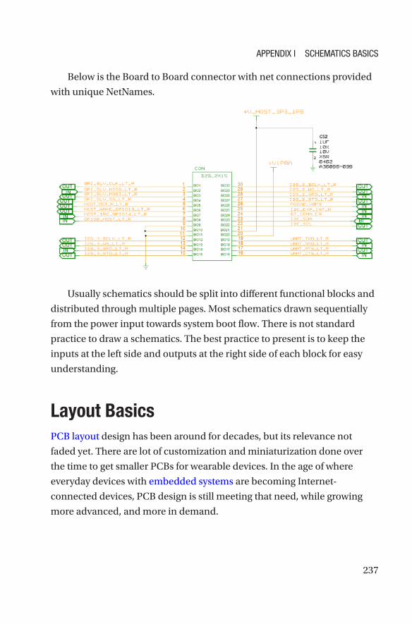
237
Below is the Board to Board connector with net connections provided
with unique NetNames.
Usually schematics should be split into different functional blocks and
distributed through multiple pages. Most schematics drawn sequentially
from the power input towards system boot flow. There is not standard
practice to draw a schematics. The best practice to present is to keep the
inputs at the left side and outputs at the right side of each block for easy
understanding.
Layout BasicsPCB layout design has been around for decades, but its relevance not
faded yet. There are lot of customization and miniaturization done over
the time to get smaller PCBs for wearable devices. In the age of where
everyday devices with embedded systems are becoming Internet-
connected devices, PCB design is still meeting that need, while growing
more advanced, and more in demand.
APPENDIX I SCHEMATICS BASICS

238
Despite so much advancements in the PCB technology and the design
tools, the layout CAD design still same. Skilled CAD design engineers have
to do manually place and route the connections in a PCB.
Its absolute necessary for an engineer working on systems designs to
learn about printed circuit boards.
First step is setting up the layers as per the plan in the Layout tool.
Fix the board outline along with the layer details. Import the netlist from
the schematics design. All the schematics symbols shown above will be
imported in the layout with equivalent layout symbols along with the
reference designators and properties.
Once component are imported along with the connection details,
finish the component placement as per the floor plan. Freeze the
placement as per the system requirements.
Start the signal routing as per the guidelines. Do the power routing at
the end.
Designers can view the board file on the Layout viewer, navigate layer
by layer and make sure everything done as per electrical guidelines. Do not
violate laws of physics anywhere in the design.
Electronic System Design Communication interfacesInterfacing the electronic system allows the electronic circuit or system
to communicate internally and externally. The communications interface
allows the transmission of either analogue signals or digital data.
Each electronic system communicates with other systems by
transmitting data via a transmitter (Tx) subsystem and receives data via
a receiver (Rx) subsystem. The medium between the two systems is the
communications channel. However, when analogue signals or digital data
are transmitted through the communications channel, noise might be
APPENDIX I SCHEMATICS BASICS

239
added to the signal, potentially corrupting the data. A great deal of care
must be taken to ensure that the electronic systems do not use corrupted
information.
Although information can be sent or received as analogue signals or
digital data, digital data transmission is increasingly common and occurs
as either parallel or serial data transmission:
Parallel data transmission. Multiple bits of data are transferred
simultaneously, allowing high-speed data transfer.
Serial data transmission. One bit of data is transferred at a time (a
serial bitstream). Serial data transmission takes longer, but when the data
is transmitted on electrical wires (typically copper wires), fewer wires are
required than with the parallel data transmission. Serial data transmission
also lends itself to data transmission via optical fibers and wireless
methods.
Many systems allow several parallel and serial communications
standards.
For the synchronous data transfer, a separate clock is shown for the
transmitter and receiver. In practice, there might only be one common
clock for the transmitter and receiver.
During data transmission, errors can occur when noise is added to
the signal and when the noise is large enough to corrupt the data being
transmitted. The transmitter circuit can include the ability to add information
to the data before they are transmitted, and the receiver circuit can include
the ability to identify whether the data it has received appears to be OK or has
been corrupted. A simple method for error checking is to use parity checking,
in which a bit is added and transmitted with the data. Considering a byte of
data (8 bits) as an example, parity checking is of two types:
Odd parity coding will set the parity bit to a logic 1 if the number of
logic 1s in the byte is even, so that the total number of logic 1s is an odd
number. If the receiver receives an odd number of logic 1s, then it will
identify that the byte was transmitted correctly.
APPENDIX I SCHEMATICS BASICS

240
Even parity coding will set the parity bit to a logic 1 if the number of
logic 1s in the byte is odd, so that the total number of logic 1s is an even
number. If the receiver receives an even number of logic 1s, then it will
identify that the byte was transmitted correctly.
Parity checking is a rudimentary method, and most communications
systems include more sophisticated capabilities.
The characteristics of the channel must also be considered, the data
may need to be modulated before transmission. Modulation takes either of
two forms:
Baseband signals in digital are the 1s and 0s being generated. On a PCB
and communicating between ICs on the PCB, baseband signals are used.
These signals cover a frequency range from DC to an upper frequency
value.
Modulated signals are baseband signals that have been modulated by
a carrier signal so that the entire signal is now at some higher frequency.
Modulation allows the baseband signals to be transmitted through
a particular communications channel. When modulated signals are
transmitted and received, the electronic system must include a modulator
and a demodulator.
The transmission of the signal through the communications channel
can be either one-way or two-way, so the designer must decide whether
the communication is to be simplex, half-duplex, or full-duplex:
Simplex, in which data transmission is one-way on a single channel.
Half-duplex, in which data transmission is two-way on a single
channel. This means that the direction of data transmission alternates, so
that the system would be able to receive or transmit, but not both at the
same time.
Full-duplex, in which data transmission is two-way on two channels.
This means that an electronic system would be able to receive or transmit
at the same time.
Finally, the signal will be transmitted through the communications
channel via electrical wires, optical fibers, or using wireless methods.
APPENDIX I SCHEMATICS BASICS

241
Wired, in which metal wires, typically copper, are used to transmit the
electrical signal.
Optical fiber, in which an electrical signal is converted to an optical
(light) signal and transmitted along the optical fiber. This allows high
transmission rates and low loss, so that signals can be transmitted over
long distances, and a low bit error rate. The electrical signal is generated
either by a light-emitting diode (LED) creating noncoherent light or by a
laser creating coherent light. At the receiver end, the signal is converted
back to an electrical signal using a photodiode or phototransistor.
Wireless, in which an electrical signal is modulated and applied to
an antenna. The more popular modulation methods are AM (amplitude
modulation), FM (frequency modulation), and PM (phase modulation).
The signal is transmitted through free space, and at the receiver, another
antenna picks up the transmitted signal, demodulates it, and restores it. It
must then be amplified before it can be used.
High Speed InterfacesHigh-speed serial interfaces are successful in chips due to demand for high
bandwidth and performance of electronic devices. Various standards are
developed around different high speed interfaces in a single monolithic
IC. However, different standards also have different requirements and
from a silicon design perspective. Creating a high speed interface cell that
meets the requirements of different standards becomes a smart design
proposition.
Only by understanding the differences among emerging high-
speed interface standards and the tradeoffs involved in a common
implementation will the system designer will better be able to choose the
right device for his application.
APPENDIX I SCHEMATICS BASICS

242
Basically, a given high speed link can be modeled with three elements:
the transmitter, a channel that propagates the signal, and a receiver:
The channel may be as simple as a pc board trace used to interconnect
two chips or it may be much more complicated - for example, for a WAN
backplane application the "channel" may have multiple lengths of pc
board trace joined by connectors. For long-reach standards the channel
may also have optics since long reach is required.
In an ideal system, the edges of a digital signal will always occur at
integer multiples of the signal period. In a real system, the edges of a digital
signal will occur in a distribution around the center point, which is the
average period of the digital signal.
Jitter is defined as the variation in the edge placement of a digital
signal. Three jitter components are usually specified: jitter generation,
jitter tolerance, and jitter transfer. Jitter generation is the amount of jitter
created by a device assuming the device's reference clock to be jitter-free.
Jitter tolerance is the maximum amount of jitter a device can withstand and
still reliably receive data. Jitter transfer is a measure of the amount of jitter
transferred from the receive side of a device to the transmit side of a device.
Jitter requirements for high-speed interface standards vary widely.
Deterministic jitter is jitter generated by either insufficient channel
bandwidth, leading to inter-symbol-interference, or by duty-cycle
distortion, which leads to timing errors in data clocking. Random jitter
is usually assumed to have a Gaussian distribution and is generated by
physical noise such as thermal noise. Sinusoidal jitter is used to test the
jitter tolerance of a receiver across a range of jitter frequencies and is not a
jitter type that would be encountered in a deployed system.
Multiple approaches to meet the jitter requirements can be taken.
Since many of these high-bandwidth interfaces use source-synchronous
clocks, the jitter in the generated clock is of concern. Such systems benefit
from using a high-quality crystal and PLL to generate the board clock used
to clock most of the system logic, since clocks recovered from the received
data usually have high jitter relative to a quality crystal oscillator.
APPENDIX I SCHEMATICS BASICS

243
Pre-emphasis may be applied to the output signals to ensure the
received signal has a well-defined shape after the frequency-dependent
deleterious effects of the channel are taken into consideration. PLLs
required by the clock-and-data-recovery circuits in the receivers must
be able to accurately track the input data. The receivers may also use
equalization to reshape the received pulse and "open the eye" of the
received signal.
Pulse-shapingThe pre-emphasis and equalization techniques described above are
methods of pulse-shaping where the shape of the waveform is modified to
"open-up" the eye diagram. Pre-emphasis is done by emphasizing the high
frequency content of the output waveform and is done by the transmitter.
Equalization is done by emphasizing the high frequency content of the
input waveform and is done by the receiver. The emphasis on the high-
frequency content is required since the channel frequency response is a
low-pass response.
One simpler common pre-emphasis technique is to temporarily
increase the rail voltage of the transmitter for 0-1 or 1-0 transitions. With
this technique the rise and fall times for the circuit are accelerated, since
after the transition the output is allowed to "settle" to a voltage closer to
the common-mode voltage for a continuous run of common symbols.
This technique has the advantage of requiring minimal circuit area to
implement, since it can be done using digital logic — complex analog
filters are not required.
An example differential interface architecture used by many CMOS
differential circuits, The transmitter may be AC- or DC-coupled to the
receiver. For DC-coupling, the transmitter output lines are directly
connected to the receiver input lines - so any DC voltage on the transmitter
APPENDIX I SCHEMATICS BASICS

244
output line is presented to the receiver input line. The common-mode
voltage of a DC-coupled receiver will therefore vary as the common-mode
voltage of the transmitter varies.
For an AC-coupled link, the transmitter output lines are connected
to the receiver input lines through series capacitors, which serve as DC-
blockers. An AC-coupled receiver can control its common-mode voltage,
since the AC-coupling capacitor serves as a DC block - the transmitter
cannot vary the common-mode voltage of the receiver. AC-coupling is
possible because the maximum run-length (number of consecutive 1s or
0s) of the subject protocol is limited (the pattern must be DC-balanced).
When the maximum run-length of a protocol is too large, AC-coupling is
not possible.
The differential transmitter is paired with a differential receiver -
however, while the differential transmitter architecture is relatively
standardized there are many different differential receiver architectures
in use. A DC-coupled example receiver architecture coupled to the
differential transmitter.
One of the advantages of an AC-coupled high-speed link is the control
the receiver designer has over the common-mode voltage - the designer
can optimize the receive circuit for a specific common mode voltage,
because the input signals will not have any DC component. As a result,
the jitter requirements of a particular specification can potentially be met
with more margin with an AC-coupled receiver than with a DC-coupled
receiver.
The result is that the design of a DC-coupled transmitter may be easier
than an AC-coupled transmitter for the same set of specifications. Also, the
design of an AC-coupled receiver will be easier than the design of a DC-
coupled receiver for the same set of specifications.
APPENDIX I SCHEMATICS BASICS

245
Reliability/durabilityThe primary concern for reliability is ESD protection. Since the I/Os for
multi-gigabit standards are by definition high data rate, the I/O must have
low capacitance. The requirement for low capacitance leads to novel ESD
structures to ensure the I/Os are fully protected without introducing the
deleterious effects on rise time which result from high capacitance. Such
effects include a decrease in supported bandwidth and increases in jitter
and power consumption.
Low Speed Communication InterfacesThe most common low speed communications interfaces are I2C, SPI
and UART.
The main difference between synchronous interfaces (like the SPI
or I2C) and the asynchronous ones (like the UART) is in the way the
timing information is passed from transmitter to receiver. Synchronous
communication peripherals need a physical line (a wire) to be dedicated
to the clock signal, providing synchronization between the two devices.
APPENDIX I SCHEMATICS BASICS

247© Neeraj Kumar Singh, Porselvan Muthukrishnan, Satyanarayana Sanpini 2019 N. K. Singh et al., Industrial System Engineering for Drones, https://doi.org/10.1007/978-1-4842-3534-8
APPENDIX II
ReferencesThe electrical hardware system design is complex and requires multi-
disciplinary expertize. The system quality, durability and cost are
dependent on the choices made by the architect.
To familiarize himself on multiple aspects not fully covered in this
book, the reader is encouraged to go through following references on
circuit design, schematics design, layout design, testing, validation and
certification.
http://www.circuitbasics.com/make-custom-pcb/
https://www.pcbcart.com/article/content/pcb-assembly-
process.html
https://www.hackster.io/muunbo/how-to-bring-up-a-pcb-cb2a78
https://www.fedevel.com/welldoneblog/2013/10/9-steps-to-
bring-up-a-freescale-i-mx6-board-to-life/
https://emcfastpass.com/emc-testing-beginners-guide/emissions/
http://airborn.com.au/method/layout.html
http://www.omnicircuitboards.com/blog/bid/289774/
Understanding-PCB-Manufacturing-Multilayer-Assembly
https://www.propertycasualty360.com/2016/04/28/14-
things- you-need-to-know-about-commercial-drones/?slretu
rn=20180816080124
https://www.wired.com/story/guide-drones/
https://wpo-altertechnology.com/drones-product-safety/
http://www.omnicircuitboards.com/blog/bid/289774/Understanding-PCB-Manufacturing-Multilayer-Assembly

248
https://blog.assentcompliance.com/index.php/what-is-product-
compliance/
https://www.dekra-product-safety.com/en/solutions/chemical-
safety- testing
http://www.tracglobal.com/content/emission-testing
https://www.worldscientific.com/worldscibooks/10.1142/10241
https://top-10-drones.com/blog/choose-motor-propeller-
quadcopter/
APPENDIX II REFERENCES

249© Neeraj Kumar Singh, Porselvan Muthukrishnan, Satyanarayana Sanpini 2019 N. K. Singh et al., Industrial System Engineering for Drones, https://doi.org/10.1007/978-1-4842-3534-8
Epilogue
We set out with a goal of providing good overview and introduction
to electrical system design. Reader is taken through fascinating and
challenging world of system design, starting from design flow till
certification considerations. Drone system example is considered as it
encompasses multiple aspects like industrial design, mechanical design,
electrical hardware design and real time software designs. Hopefully we
succeeded, to a large extent, in providing firm footing, so that reader can
explore further on his own.
To develop further expertize and appreciation for the subject matter,
reader is encouraged to take up study of few additional embedded system
examples like set top box, WiFi routers, IoT systems for home automation,
surveillance etc. Studying standard teardown reports is good way to start
with. Even more effective approach would be to do a hands on high level
design of a small system that addresses a specific need in the real world,
however small it may be.

251© Neeraj Kumar Singh, Porselvan Muthukrishnan, Satyanarayana Sanpini 2019 N. K. Singh et al., Industrial System Engineering for Drones, https://doi.org/10.1007/978-1-4842-3534-8
Index
AActive cooling solutions, 99Active power management, 185Advanced configuration and power
interface (ACPI), 183Agile model, 172AHr (ampere hour)/WHr
(watt hour), 57Altitude simulation testing, 224Assembly process, 142
design specifications of, 143inspection and functional test, 149manual soldering, 148post process, 149, 150pre-gerber files, 143surface mount, 144
hole connectors, 148inspection and quality
control, 146inspection method, 147manual checks, 146pick and place, 145reflow soldering, 145soldering process, 149solder paste, 144wave soldering, 148X-ray check, 147
BBaseband signals, 240Batteries/solar/fuels, 95
architecture, 98lead acid, 96lithium, 97NiCd, 96NiMH, 96power consumption, 97rechargeable batteries, 96specifications, 98
Battery estimation, 55capacity, 56cells/voltage, 55cell voltage and packs, 56chemistry, 55constraints, 55initial and lifetime costs, 57watt hours and energy density, 57
Bill of materials (BOM), 35–37component, 119generation, 122material readiness, 123report-type document, 119symbol attributes, 121time-consuming process, 120tool-generated BOM, 120

252
Black box testing, 209Board-level testing (BLT)
BIOS, 154flash programming, 154functionality check, 155OS and application
installation, 155Board-to-board (BTB)
connectors, 103Bringing-up system, 139
drivers/modules, 204–207libraries/middle layer and
application, 208loading and unloading
process, 204OS (RTLinux), 203SoC block diagram, 206system firmware, 203
CCache memory, 67Cameras
categories, 88color sensors, 89crop monitoring drone, 90drone imaging solution, 91features of, 91hyperspectral imaging
sensor, 90, 92integration of, 88monochrome sensors, 89power source and host
interface, 90
spectral imaging, 89Clock-and-data-recovery circuits, 243Color sensors, 89Communication module, 83
electronic system, 84features of, 87intentional and unintentional
radiation, 84IR/RF wireless, 86key considerations, 86mobile network, 85module interfaces, 83solution, 87WiFi+BT, 84, 85wireless protocols, 83
CompactFlash storage, 77Computer-aided design (CAD)
tool, 19Connected standby power
management, 185–187Cooling technologies, 99Costing testing, 230Cathode ray oscilloscope (CRO), 153Crop Squad specification, 23, 24
DData acquisition (DAQ)
equipment, 160Design constraints, 133Design rules checking (DRC), 118Design validation testing
electrical validation, 161integration testing, 162
INDEX
253
optional circuits, 162signal integrity
testing, 161, 162power validation
design margins, 157efficiency measurement, 158power and performance,
160, 161power integrity, 158power supplies, 157system power targets, 160test specification, 157thermal device, 159
validation processes, 157Drone system
accessories, 15assembly
factory tooling, 164standard/customized
parts, 163system pilot build, 164system validation, 163
classification, 2commercial field, 3ground-based controllers and
accessories, 14, 15hardware, 4–10industrial option, 3logical view, 12mechanical system, 12–14military applications, 2software, 10–12
Drop, shock, and vibration testing, 224
E
Electrical fast transient (EFT) test, 222Electronic system design
baseband signals, 240error checking, 239full-duplex, 240half-duplex, 240implex, 240modulated signals, 240modulation methods, 241optical fiber, 241parallel data transmission, 239parity checking, 240parity coding, 240serial data transmission, 239Tx and Rx, 238wireless, 241
embedded multimedia controller (eMMC), 77
Electromagnetic compatibly (EMC), 219
End-to-end testing, 211Environmental testing certification
altitude testing, 224drop, shock, and vibration
testing, 224humidity, 223product designers, 222reliability, 225temperature, 223
Electrostatic discharge (ESD), 221Ethernet, 103External displays, 93
Index

254
FFabrication process manufacturing
process, 140–142Field programmable gate array
(FPGA), 94Flash storage device
advantages of, 75compactflash, 76Micro SD card, 79MMC/SD card, 78multimedia card, 77NOR vs. NAND flash, 76secure digital, 78solid state drives, 79, 80USB flash drive, 80, 81
Flight controllers, 94, 95FPC/FFC connection, 105Functional testing, 210
GGlobal system power states and
transitions, 188Gray box testing, 210
HHardware design
ball grid array, 5electrical ingredients selection
BOM and components, 35–37electrical BOM (EBOM), 36feature, 35production status, 36
features of, 8, 9floor plan, 43–45PCBA design, 4
dimensions, 38, 39hybrid PCB, 39layer stack-up, 40–42parameters, 37types, 38–40
power architecturebatteries, 55–58comparison of, 49complexity, 50cost and size, 50devices, 48efficiency, 49estimation, 45function, 49linear regulators, 48map, 50–52platform requirements, 47ripple and noise, 50sequencing data, 53–55SOC voltage and current
requirements, 45states, 44switching regulators, 48
process of, 32requirements, 33, 34SOC, 5, 6subsystems/electrical subsystems
communication devices, 7–10input, 6output, 7storage, 7
INDEX

255
Hardware development, 111High-speed serial interfaces
AC-coupled, 244DC-coupled, 244elements, 242ideal system, 242jitter components, 242jitter requirements, 242pre-emphasis technique, 243pulse-shaping technique, 243real system, 242reliability/durability, 245transmitter, 243, 244
Hyperspectral imaging. See Spectral imaging
IIndustrial design (ID), 26Idle power management, 185Immunity testing, 220Incremental, iterative, and agile
models, 171–173Ingredients, 63
batteries, 95–98camera, 88–92communication module, 87–92display, 92–95
external, 93internal, 92key considerations, 93
flight controllers, 94, 95interconnect (see Interconnects)mechanicals, 106–108
memory system, 67–74storage solution, 83–93system on a chip, 64–66thermal solution, 99–102
Integration testing, 210Interconnects
board-to-board (BTB) connectors, 103
definition of, 101electrical connections, 102Ethernet cables, 103FPC/FFC connectors, 105key considerations, 105mini and micro USB, 103requirements, 106RF connector, 104selection of, 106wire-to-board connectors, 104
Internal displays, 92
JJitter, 242
KKeep Out Zones (KOZ), 132
LLayout design
auto route, 123board outline, 124CAD PCB layout, 123
Index

256
electrical components, 123electrical constraints
capacitance, 128cross talk, 128dielectric absorption, 127impedance mismatch, 126mutual inductance, 128power integrity, 128–130proximity of, 126signal attenuation, 127signal integrity, 126skin effect, 127
layer stack-up, 124, 125mechanical constraints
component locations, 133coordinate system, 131design capabilities, 131design constraints, 133dimension, 132Keep Out Zones (KOZ), 132orientation, 132physical constraints, 133requirements, 130
NetlistGerber release, 137mechanical check, 136placement, 134, 135routing, 135, 136
trade-off, 124Lead acid, 96Light-emitting diode (LED), 241Linear regulator operates, 48Linux
ACPI methods, 196–198callback function, 194models/protocols/
specifications, 195module loading process, 205operating context/state, 194platform/system design, 196predefined methods, 196running/active state, 194standby state, 195
Lithium-Ion (Li-ion) batteries, 97Load testing, 212Logistics and operations
management, 60–61Low speed communications
interfaces, 245
MMagnetic storage devices, 74Mechanical design
Crop Squad, 25definition, 24, 26dependencies, 32monitor crops, 28purpose, 27, 28requirements
air gap, 31camera module, 31daughterboard, 31dimensions of, 28enclosures, 29flexible PCB, 31heat spreader, 30
Layout design (cont.)
INDEX

257
motherboard, 30Mylar, 30processing unit, 30propeller motor, 29shielding, 30stack-up, 28X-frame, 29
variants, 26Mechanical items
categories, 106key considerations, 108multicopter designs, 107quadcopter, 106solutions, 108
Memory systemsblock diagram, 72cache memory, 67DDR-SDRAM, 67fifth generation, 69first generation, 68fourth generation, 69key considerations, 70layer of, 67load and prolonged operation, 71mobile DRAM, 69parameters, 70requirements, 73second generation, 68third generation, 68
Microcontroller/microprocessor, 94Mobile network, 85Modulated signals, 240Monochrome sensors, 89Multimedia card (MMC), 77
NNetlist generation, 119Nickel Cadmium (NiCd), 96Nickel Metal Hydride (NiMH), 96Non-functional testing, 211
OOptical storage devices, 74
P, QParallel data transmission, 239Passive cooling techniques, 100Performance testing, 211Physical constraints, 133Pilot systems, 139Pilot testing, 225Power integrity (PI), 128–130Power management system, 194Power-on
firmware/software, 153generation of, 152input power requirement, 152inspection, 151preliminary and sanity
checks, 150sequencing and reset check, 153short-circuit checks, 151variation of, 151
Pre-emphasis technique, 243Product requirement document
(PRD), 18
Index

258
Printed circuit board assembly (PCBA), 4, 111
Printed circuit board (PCB), 104assembly process, 142–150fabrication process, 140–142layout design, 237library development
footprint creation, 115, 116footprint verification, 116logical symbol creation,
113, 114symbol creation, 112symbol verification, 114time-consuming task, 112visual representation, 113
PCBA, 112Product certification/
qualification, 215accessories cost, 231device costing, 230environmental certification
(see Environmental testing certification)
product certification centers, 230product ecology, 226
California Proposition 65, 229EU REACH, 229ISO, 230prohibited substances, 226ROHS, 228WEEE, 230
production cost, 231registration, 232regulations, 215, 231
regulatory certificationbattery, 218chemical safety
certification, 218conducted emissions, 220conducted voltage, 221EFT immunity test, 222electrical safety testing, 217electronic devices, 216emission testing, 219electrostatic discharge
(ESD), 221functional safety, 217immunity testing, 220mechanical check, 218products and
characteristics, 216radiation testing, 220, 221safety, 216
service and support, 225–226Pulse-shaping technique, 243
RRadiation testing, 220, 221Radio-frequency (RF), 105Real-time operating system
(RTOS), 176Regression testing, 211Restriction of Hazardous
Substances Directive (ROHS), 228
RTLinux system architecture, 176
INDEX

259
S
Schematics designbest practice, 237capture, 117, 118definition, 233design rules, 118Netlist generation, 119nets, 233reading, 236reference circuit, 118reference designator, 117representation of, 116symbols, 234
Secure Digital (SD), 78Security testing, 212Serial data transmission, 239Smoke and sanity testing, 210Software architecture, 58–60
application components, 60categories, 58firmware components, 58OS and drivers, 59sensing, navigation and control, 59
Software development life cycle (SDLC), 168
incremental, iterative, and agile, 171–173
software development models, 169
stages/steps, 168V-shaped model, 170waterfall model, 169, 170
Software development process, 167
ACPI states, 187active power management, 185connected standby power
management, 185–187considerations, 180device states, 191global and system states, 188–190idle power management, 185key attributes, 181Linux power management,
193–198low power
HW considerations, 182, 183power consumption, 183, 184power optimization, 184SW considerations, 183
power state, 192processor power states, 193real-time system, 198–202requirements, 180SDLC (see Software development
life cycle (SDLC))software stack, 173–180system bring-up, 202–208verification, validation, and
maintenance, 208–212mechanism, 209methodology, 209testing level, 210–212
Software stackapplication layer, 180architecture, 179components, 173firmware and device, 174, 175
Index

260
hardware, 174operating system, 176, 177RTLinux design, 177–179RTLinux operating system, 177SDK and libraries, 180
Solid State Drives (SSD), 79, 80Spectral imaging, 89System requirement document
(SRD), 18Static random-access memory
(SRAM), 67Storage device
eMMC and uSSD, 81features of, 82flash storage, 75–80key parameters, 81magnetic storage, 74nonvolatile memory, 73optical storage, 74SDXC format, 81storage solution, 82, 83
Storage temperature, 36Stress testing, 212Switching regulators operate, 48Synchronous vs. asynchronous
interfaces, 245Synchronous dynamic random-access
memory (SDRAM), 67System design flow, 1, 17
architecture, 19
hardware block diagram, 22, 23mechanical concept, 19–21software, 22
aspects, 18implementation, 23logistics and operations
management, 60, 61mechanical design (see
Mechanical design)requirement specification, 18software architecture, 58–60specifications of, 23, 24
System-on-a-chip (SOC), 53categories, 65component, 64key considerations, 66solutions, 66
System pilot build, 164System power map, 52–54System testing, 211System validation testing, 163
TTheoretical calculations, 159Thermal solution
active cooling solutions, 99architectural design, 99categories, 99key features, 100passive cooling techniques, 100solution, 101
Software stack (cont.)
INDEX

261
UUnit testing, 210Universal Serial Bus (USB)
connection, 102Unmanned aerial vehicle
(UAV), 2USB memory stick, 80, 81User acceptance testing
(UAT), 211
VV-shaped model, 170
W, X, Y, ZWaterfall model, 169, 170White box testing, 210WiFi+BT, 84, 85Wire-to-board connection, 104
Index