Improving Reconfigurable Systems Reliability by Combining Periodical Test and Redundancy Techniques:...
12
JOURNAL OF ELECTRONIC TESTING: Theory and Applications 17, 163–174, 2001 c 2001 Kluwer Academic Publishers. Manufactured in The Netherlands. Improving Reconfigurable Systems Reliability by Combining Periodical Test and Redundancy Techniques: A Case Study EDUARDO AUGUSTO BEZERRA Space Science Centre, School of Engineering and Information Technology, University of Sussex, UK; Informatics Faculty, Catholic University – PUCRS, Brazil [email protected] FABIAN VARGAS Electrical Engineering Department, Catholic University – PUCRS, Brazil [email protected] MICHAEL PAUL GOUGH Space Science Centre, School of Engineering and Information Technology, University of Sussex, UK [email protected] Received November 21, 2000; Revised February 28, 2001 Editors: V.H. Champac and M. Lubaszewski Abstract. This paper revises and introduces to the field of reconfigurable computer systems, some traditional techniques used in the fields of fault-tolerance and testing of digital circuits. The target area is that of on-board spacecraft electronics, as this class of application is a good candidate for the use of reconfigurable computing technology. Fault tolerant strategies are used in order for the system to adapt itself to the severe conditions found in space. In addition, the paper describes some problems and possible solutions for the use of reconfigurable components, based on programmable logic, in space applications. Keywords: reconfigurable computing, fault tolerance, test, programmable-logic-array, and space applications 1. Introduction The on-board computer system of a spacecraft for long-life missions is a good representative example of an adaptive system [9, 20]. This category of sys- tem, including software and hardware, has to be de- signed considering that post-launch maintenance is generally impractical [20], and the hardness of the space environment will certainly cause problems to the system. Traditional on-board computers based on microprocessors, adapt to the problems they face by using fault-tolerance techniques. Faults are tolerated, and vital services such as, for instance, communication to ground stations, are maintained operative. From the hardware point of view, the adaptation takes place by the isolation of faulty modules from the system, and, where it is possible, by the activation of spare mod- ules. At the software level, the adaptation is identified, basically, when the microprocessor starts using a new program, stored on-board or up-loaded from ground. Reconfigurable devices introduce to the hardware level, the flexibility for adaptation provided at the software level [19, 25]. In the case of space ap- plications, two important advantages of having the
-
Upload
independent -
Category
Documents
-
view
2 -
download
0
Transcript of Improving Reconfigurable Systems Reliability by Combining Periodical Test and Redundancy Techniques:...
JOURNAL OF ELECTRONIC TESTING: Theory and Applications 17, 163–174, 2001c© 2001 Kluwer Academic Publishers. Manufactured in The Netherlands.
Improving Reconfigurable Systems Reliability by Combining Periodical Testand Redundancy Techniques: A Case Study
EDUARDO AUGUSTO BEZERRASpace Science Centre, School of Engineering and Information Technology, University of Sussex, UK;
Informatics Faculty, Catholic University – PUCRS, [email protected]
FABIAN VARGASElectrical Engineering Department, Catholic University – PUCRS, Brazil
MICHAEL PAUL GOUGHSpace Science Centre, School of Engineering and Information Technology, University of Sussex, UK
Received November 21, 2000; Revised February 28, 2001
Editors: V.H. Champac and M. Lubaszewski
Abstract. This paper revises and introduces to the field of reconfigurable computer systems, some traditionaltechniques used in the fields of fault-tolerance and testing of digital circuits. The target area is that of on-boardspacecraft electronics, as this class of application is a good candidate for the use of reconfigurable computingtechnology. Fault tolerant strategies are used in order for the system to adapt itself to the severe conditions foundin space. In addition, the paper describes some problems and possible solutions for the use of reconfigurablecomponents, based on programmable logic, in space applications.
Keywords: reconfigurable computing, fault tolerance, test, programmable-logic-array, and space applications
1. Introduction
The on-board computer system of a spacecraft forlong-life missions is a good representative exampleof an adaptive system [9, 20]. This category of sys-tem, including software and hardware, has to be de-signed considering that post-launch maintenance isgenerally impractical [20], and the hardness of thespace environment will certainly cause problems tothe system. Traditional on-board computers based onmicroprocessors, adapt to the problems they face byusing fault-tolerance techniques. Faults are tolerated,
and vital services such as, for instance, communicationto ground stations, are maintained operative. From thehardware point of view, the adaptation takes place bythe isolation of faulty modules from the system, and,where it is possible, by the activation of spare mod-ules. At the software level, the adaptation is identified,basically, when the microprocessor starts using a newprogram, stored on-board or up-loaded from ground.
Reconfigurable devices introduce to the hardwarelevel, the flexibility for adaptation provided at thesoftware level [19, 25]. In the case of space ap-plications, two important advantages of having the
164 Bezerra, Vargas and Gough
whole computer system, including the hardware andthe software parts, implemented using only hardwarecomponents (reconfigurable hardware) are: the econ-omy in area usage and board complexity; and the in-creased processing speed with lower clock rates.
On-board systems based on reconfigurable hardwarewill also reduce the overall design cost associated withthis category of computer. Because of the applicationspecific nature of this kind of system, its requirementscan vary significantly from application to application,resulting in a completely new design for almost everynew application. Reconfigurable devices are appropri-ate for the implementation of application specific solu-tions. This allows the designers to have different hard-ware configurations, without the need for changes inthe board layout. It is another example of adaptation.In this case the hardware adapts to a new applicationnot because of the occurrence of a fault, but because ofa new mission requirement.
The drawback to the use of reconfigurable devicesis the difficulty associated with the “software” devel-opment for this kind of hardware. The internal organ-isation of the reconfigurable devices available, makesthe development of good synthesis tools for high levelprogramming languages an arduous job. Even whenusing hardware description languages as, for instance,VHDL, the developer of spacecraft computers has tokeep the code as simple as possible, in order to avoidproblems for the synthesis tool [3]. For instance, insystems that require complex data structures or manylevels of nested loops, the best solution maybe to stilluse conventional microprocessor based boards.
The first concern of a designer of a reconfigurablesystem for long-life space applications is the improve-ment of system dependability features such as, forexample, reliability, availability, maintainability andtestability [22]. Reliable devices together with fault-tolerance and test strategies are used in order to ac-complish this target. In the past few years, strategies toimprove the dependability features of reconfigurablecomputer systems, have been proposed and imple-mented [4, 9, 11, 13, 14, 23, 24]. These strategies aremainly based on the traditional ones used in micropro-cessor based systems.
Following a similar approach, in this paper strategiesto improve the dependability of reconfigurable com-puting systems for space applications are presented.An important consideration is to define the strategiesthat make use of the fact that reconfigurable comput-ing permits new possibilities, for instance, the use of a
combination of strategies for fault tolerance in softwareand in hardware at the same level of abstraction. Theideas discussed here can be used not only for space ap-plications, but also for any other embedded system withsimilar dependability requirements. It is important tohighlight that all strategies discussed in this work areto be applied during the system’s usage and at a highlevel of abstraction. The fault detection activities takeplace first at component level and then at the networknode level. The diagnosis (location) of faults inside acomponent is an interesting activity from the manufac-turers’ point of view and it is out of the scope of thiswork. This position can be explained because there is ahuge effort from the user point of view to isolate faultyparts internally to a component. Instead of this, it ismore interesting for the user to try to recover the wholecomponent, which is possible if the application is basedon SRAM-type FPGA components.
This paper is organised as follows. Section 2describes a case study which is one of the motivationsfor this work. Section 3 describes the basic node ofa network architecture for space applications, basedon reconfigurable devices. In Section 4 there is a de-scription of the fault model adopted, and a brief re-view of Single Event Upset (SEU), which is one ofthe main sources of problems in on-board electronicsin space applications. Section 5 introduces strategiesfor dependability improvement, with emphasis on re-liability, availability and testability improvement tech-niques. Section 6 describes an approach for maskingconnectivity faults. Section 7 presents implementationdetails. Section 8 discusses expected results. In Sec-tion 9 there are some conclusions, and future directions.
2. Motivation for the Use of FPGAsin Space Applications
The main motivation for using FPGAs instead of micro-processors for on-board computer implementation, isthe gain in performance with associated decrease in thePCB area usage. In order to find out the feasibility of us-ing FPGAs in this class of application, a case study wasdeveloped. The case study is the FPGA implementa-tion of an on-board instrumentation module of a NASAsounding rocket [5]. This rocket flew from Spitzbergen,Norway, in the winter of 1997/1998, carrying a scien-tific application computer designed at the Space Sci-ence Centre, University of Sussex [10]. The real timescience measurement performed by this embedded

Improving Reconfigurable Systems Reliability 165
system is an auto-correlation function (ACF) [2]processing of particle count pulses as a means of study-ing processes occurring in near Earth plasmas. Theoriginal module as flown consisted of a board withtwo DS87C520 microcontrollers (8051 family), FIFOs,state machines and software written in assembly lan-guage. Although this ACF implementation is a veryspecific application, the system as a whole, includingthe hardware and the software parts, is not too dif-ferent from conventional embedded systems based onmicroprocessors or microcontrollers. This case studyis a typical memory transfer application, with a highinput sampling rate and with scarceness of processingmodules. The most demanding actions for processingblocks, are the ones with multiply-and-accumulate op-erations (MACs), typical of DSP applications.
The test strategies proposed in this paper are de-signed to execute in parallel with the user applicationand with the fault-tolerance strategies. When consider-ing processing time, there are no performance penal-ties, because there is no need, for instance, to timeshare tasks. Table 1 lists the number of cycles neces-sary to run the processes written in assembly languagefor the microcontrollers, and the equivalent ones writ-ten in VHDL for the FPGA. The software algorithmflown on the example mission was broken down intosix contributing processes to ease the comparison.
Another important system feature improved becauseof the use of configurable computing technology is thereduction in the number of hardware components. Themain system repercussions are the reduction in the on-board area usage, and in the power consumption. Thereduction in the number of components can be achievedby using only one FPGA device configured to executethe same functionality as the whole 8051 based system.For instance, external chip FIFOs were replaced bycircular FIFOs implemented using data structures inVHDL.
Table 1. Performance comparison for the case study.
µcontroller FPGA(cycles) (cycles) Rate
P1 4,518 1 4,518 times faster
P2 8..36 1 8 to 36 times faster
P3 18..1,018 1..68 18 to 14.97 times faster
P4 1,240 48 25.8 times faster
P5 1,334..3,438 132..143 10.11 to 24 times faster
P6 11,116 288 38.6 times faster
Fig. 1. Block diagram of the proposed system. (a) Network archi-tecture. (b) Basic RCM node.
Considering the use of the FPGA board in an ap-plication where fault-tolerance is not a requirement,as the original case study, all of the electronics boardcan be implemented as a single chip, for instance, anXQ4085XL Xilinx FPGA [5, 26] with two XQ1701Lserial ROMs to store the bitstream. The result is a re-duction from 22 to 3 chips. Extrapolating the case studyto a long-life system, where fault-tolerance is required,we can use a board similar to the one shown in Fig. 1(b).In this case the reduction in the number of componentsmay be from 22 to about 10 chips on-board, which isstill a significant result, considering that now the sys-tem has fault-tolerant capabilities.
3. System Description Overview
Field-programmable gate arrays (FPGAs) are the de-vices used for the implementation of reconfigurable

166 Bezerra, Vargas and Gough
computer systems. The block diagram in Fig. 1(a)shows the proposed architecture for an on-board pro-cessing system, based on FPGAs, which may be usedfor both scientific and commercial space applications.The two main improvements in this architecture overthe architectures that have been used in most spaceapplications previously, are the use of reconfigurabledevices as the main processing elements, and the use ofa network to connect the different modules. As the mainobjective of this paper is to discuss and to present strate-gies for the dependability improvement of processingelements of a reconfigurable system, we describe inthis Section a basic network node.
The block diagram of the network node shown inFig. 1(b) has two external communication channels,one for connection to the network, and the other onefor interfacing to the application. The first one has afixed number of signals, as the protocol for inter-nodecommunication is pre-defined. A microcontroller withan embedded UART is a good option for the inter-nodecommunication. The second one is defined accordingto the application requirements, and is a good exam-ple of the flexibility introduced by the reconfigurablecomputer technology.
The main responsibilities of the processing element,FPGA module in Fig. 1(b), are to construct teleme-try packets, according to the European Space Agency(ESA) standards [6], and to implement the protocol forcommunication on the on-board network system. Theprotocol used is the Controller Area Network (CAN),and the HurriCANe core, designed by ESA has beenused in the design [16].
In some applications it may be possible to transfersome or all user processing activities to the FPGA mod-ule. An example is when the on-board data-handling(OBDH) system and one (or more) of the applicationsare designed by the same group [7, 8]. In this case the“User” block shown in Fig. 1(a) may be very simple,for instance, consisting of only analog devices, sensorsand converters, as the FPGA module in Fig. 1(b) maybe used to execute all of the processing.
The microcontroller is responsible for the implemen-tation of the physical layer of the CAN protocol, con-necting the CAN core (located on the FPGA module)to the network bus. Another important activity per-formed by the microcontroller is the management ofthe reconfiguration and test of the FPGA module. Thedesign and implementation of these activities are themain objective of this work, and they are detailed inSection 5.
Other components of the Reconfigurable ComputerModule (RCM) node are a RAM memory and a pro-grammable switch. The RAM module may be attachedto the FPGA module, in order to be used by some ap-plications as a scratch area. The programmable switchis one of the single points of failure of the system (theother one is the FPGA itself), and for this reason ahighly reliable and non complex device is used.
The data pins of the microcontrollers are connecteddirectly to a voter implemented in the FPGA, and thepins used to program the FPGA are connected to theprogrammable switch. If a single discrepancy is de-tected by the voter, then the FPGA reprograms theswitch in order to select one of the two healthy mi-crocontrollers as the new configuration manager.
The microcontrollers’ embedded flash memorieshold the configuration bitstreams (CBs) for the FPGAmodule. They may be changed from the ground in caseof system upgrades or bug fixes. The microcontrollerworks as a configuration manager allowing device(s) ofthe FPGA module to be initialised from the flash mem-ories as if they were serial ROMs. The microcontrolleris also responsible for refreshing the flash memorieswhen they experience upsets. As the objective of thiswork is the improvement of the dependability featuresof the FPGA module, strategies for dependability im-provement of the microcontroller and flash memorieswill be discussed in a future work.
4. Fault Model Adopted
As the systems based on the proposed architecture havebeen conceived for long-life missions, all of the elec-tronic components must be military standard. However,as stated before, because of the hostile environmentfound in space and the long-life expected for the sys-tem, additional fault-tolerance strategies are used in thedesign, even when employing high reliability devices.In order to define the strategies, a very simple, but ef-ficient, fault model was chosen. The faults consideredin this fault model are “stuck-at” and “connectivity”(faults in interconnect resources) [22].
The main cause of stuck-at faults in space are theSingle-Event Upsets (SEUs) caused by atmospherichigh-energy neutrons [1, 17, 18]. Most of the FPGAsavailable are SRAM based, and devices implementedwith this kind of technology are sensitive to SEUs. Ba-sically, a SEU takes place when a single high-energyparticle (typically a heavy ion) strikes a sensitive nodein a memory cell, which causes the particle to loose
Improving Reconfigurable Systems Reliability 167
energy via production of electron-hole pairs, resultingin a densely ionised track in the local region of that ele-ment. It will force the affected memory cell to stay in afixed state, 0 or 1, and, consequently, stuck-at faults arethe best option to model the bit errors that can occur.
The other modelled fault, connectivity, is responsi-ble for most of the problems in a board [22] and, asdescribed later, special strategies as, for instance, busreplication and voters, are used to tolerate this problem.Connectivity faults are related to I/O and connectionresources in general. Some authors defend the posi-tion that tests in the processing elements cover also theconnectivity faults. The strategies used to prevent and,when it is not possible, to tolerate the faults, belong tothe fault model adopted, are described next in Section 5.
In [1, 18] there is a study showing the low SEU sus-ceptibility of Xilinx FPGAs. However, for some criticalapplications where human life is at a premium or whenthe whole on-board electronics is dependent on two orthree core components, then, even the low SEU sus-ceptibility must be improved. The strategies describedin the next sections are used to tolerate the effects offaults resulting of SEU occurrences. Needless to saythat in order to tolerate a fault, it is necessary first todetect the fault. Test strategies for fault detection arealso described next.
5. SEU Prevention Strategies
5.1. Refresh Operation in a Triple ModularRedundancy (TMR) FPGA System
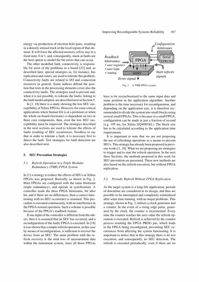
In [1] a strategy to reduce the effects of SEUs in XilinxFPGAs was proposed. Basically, as shown in Fig. 2,three FPGAs are configured with the same bitstream(triple redundancy), and operate in synchronism. Acontroller reads the three FPGA bitstreams, bit afterbit, and if there are no differences, then a correct func-tioning with no SEU occurrence is assumed. This pro-cedure is executed continuously, with no interference inthe FPGA normal operation. Such a scheme is possiblebecause of the FPGA’s readback feature.
If one input of the controller is different from the oth-ers, then it is assumed that an SEU has occurred, and areconfiguration of the faulty FPGA is executed. In [18]it was shown that a simple refresh operation, in this caseby means of reconfiguration, is sufficient to recover thedevice from an SEU. The main problem with the re-fresh recovery is the total loss of measurement datawithin the instrument system, since all those FPGAs
Fig. 2. A TMR FPGA system.
have to be resynchronised to the same input data andsame position in the application algorithm. Anotherproblem is the time necessary for reconfiguration, anddepending on the application size, it is therefore rec-ommended to divide the system into small blocks usingseveral small FPGAs. This is because in a small FPGA,configuration can be made in just a fraction of second(e.g. 195 ms, for Xilinx XQ4085XL). The block sizehas to be calculated according to the application timerequirements.
It is important to note that we are not proposingthe use of refreshing operations as a means to preventSEUs. This strategy has already been proposed in previ-ous works [1, 18]. What we are proposing are strategiesto trigger and to start the refresh operation. In the nextthree Sections, the methods proposed in this work forSEU prevention are presented. These new methods arealso based on the refresh execution, but without FPGAreplication.
5.2. Periodic Refresh Without FPGA Replication
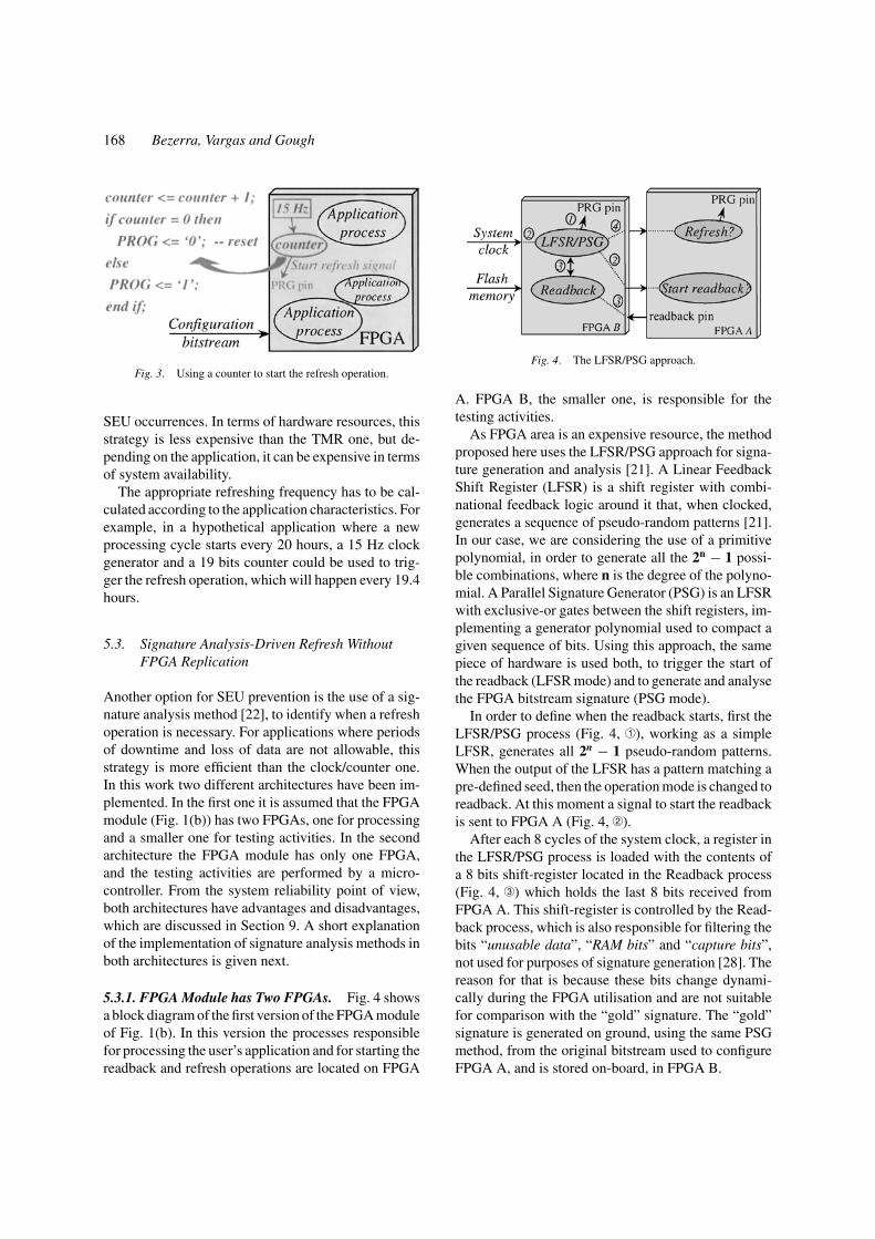
As the target system is a long-life application, periodsof downtime are considered in its design, and thus arepossible to be interrupted and completely reinitialisedafter some time running, with no major problems. Thisstrategy, shown in Fig. 3, utilises a clock generator anda counter. In the event of a rising edge pulse, gener-ated by the clock, the counter is incremented. Everytime the counter reaches the zero value the refresh op-eration is executed. Refresh is achieved by the counterprocess resetting the FPGA PROG pin, which leadsto the FPGA being reconfigured, preventing SEU oc-currences from affecting the system functioning. It isimportant to notice that in this strategy there is no testexecution, and consequently, no SEU detection. Therefresh is executed periodically, even if there are no
168 Bezerra, Vargas and Gough
Fig. 3. Using a counter to start the refresh operation.
SEU occurrences. In terms of hardware resources, thisstrategy is less expensive than the TMR one, but de-pending on the application, it can be expensive in termsof system availability.
The appropriate refreshing frequency has to be cal-culated according to the application characteristics. Forexample, in a hypothetical application where a newprocessing cycle starts every 20 hours, a 15 Hz clockgenerator and a 19 bits counter could be used to trig-ger the refresh operation, which will happen every 19.4hours.
5.3. Signature Analysis-Driven Refresh WithoutFPGA Replication
Another option for SEU prevention is the use of a sig-nature analysis method [22], to identify when a refreshoperation is necessary. For applications where periodsof downtime and loss of data are not allowable, thisstrategy is more efficient than the clock/counter one.In this work two different architectures have been im-plemented. In the first one it is assumed that the FPGAmodule (Fig. 1(b)) has two FPGAs, one for processingand a smaller one for testing activities. In the secondarchitecture the FPGA module has only one FPGA,and the testing activities are performed by a micro-controller. From the system reliability point of view,both architectures have advantages and disadvantages,which are discussed in Section 9. A short explanationof the implementation of signature analysis methods inboth architectures is given next.
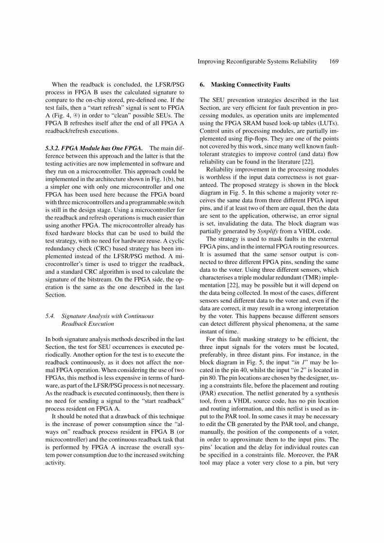
5.3.1. FPGA Module has Two FPGAs. Fig. 4 showsa block diagram of the first version of the FPGA moduleof Fig. 1(b). In this version the processes responsiblefor processing the user’s application and for starting thereadback and refresh operations are located on FPGA
Fig. 4. The LFSR/PSG approach.
A. FPGA B, the smaller one, is responsible for thetesting activities.
As FPGA area is an expensive resource, the methodproposed here uses the LFSR/PSG approach for signa-ture generation and analysis [21]. A Linear FeedbackShift Register (LFSR) is a shift register with combi-national feedback logic around it that, when clocked,generates a sequence of pseudo-random patterns [21].In our case, we are considering the use of a primitivepolynomial, in order to generate all the 2n − 1 possi-ble combinations, where n is the degree of the polyno-mial. A Parallel Signature Generator (PSG) is an LFSRwith exclusive-or gates between the shift registers, im-plementing a generator polynomial used to compact agiven sequence of bits. Using this approach, the samepiece of hardware is used both, to trigger the start ofthe readback (LFSR mode) and to generate and analysethe FPGA bitstream signature (PSG mode).
In order to define when the readback starts, first theLFSR/PSG process (Fig. 4, ✐1 ), working as a simpleLFSR, generates all 2n − 1 pseudo-random patterns.When the output of the LFSR has a pattern matching apre-defined seed, then the operation mode is changed toreadback. At this moment a signal to start the readbackis sent to FPGA A (Fig. 4, ✐2 ).
After each 8 cycles of the system clock, a register inthe LFSR/PSG process is loaded with the contents ofa 8 bits shift-register located in the Readback process(Fig. 4, ✐3 ) which holds the last 8 bits received fromFPGA A. This shift-register is controlled by the Read-back process, which is also responsible for filtering thebits “unusable data”, “RAM bits” and “capture bits”,not used for purposes of signature generation [28]. Thereason for that is because these bits change dynami-cally during the FPGA utilisation and are not suitablefor comparison with the “gold” signature. The “gold”signature is generated on ground, using the same PSGmethod, from the original bitstream used to configureFPGA A, and is stored on-board, in FPGA B.
Improving Reconfigurable Systems Reliability 169
When the readback is concluded, the LFSR/PSGprocess in FPGA B uses the calculated signature tocompare to the on-chip stored, pre-defined one. If thetest fails, then a “start refresh” signal is sent to FPGAA (Fig. 4, ✐4 ) in order to “clean” possible SEUs. TheFPGA B refreshes itself after the end of all FPGA Areadback/refresh executions.
5.3.2. FPGA Module has One FPGA. The main dif-ference between this approach and the latter is that thetesting activities are now implemented in software andthey run on a microcontroller. This approach could beimplemented in the architecture shown in Fig. 1(b), buta simpler one with only one microcontroller and oneFPGA has been used here because the FPGA boardwith three microcontrollers and a programmable switchis still in the design stage. Using a microcontroller forthe readback and refresh operations is much easier thanusing another FPGA. The microcontroller already hasfixed hardware blocks that can be used to build thetest strategy, with no need for hardware reuse. A cyclicredundancy check (CRC) based strategy has been im-plemented instead of the LFSR/PSG method. A mi-crocontroller’s timer is used to trigger the readback,and a standard CRC algorithm is used to calculate thesignature of the bitstream. On the FPGA side, the op-eration is the same as the one described in the lastSection.
5.4. Signature Analysis with ContinuousReadback Execution
In both signature analysis methods described in the lastSection, the test for SEU occurrences is executed pe-riodically. Another option for the test is to execute thereadback continuously, as it does not affect the nor-mal FPGA operation. When considering the use of twoFPGAs, this method is less expensive in terms of hard-ware, as part of the LFSR/PSG process is not necessary.As the readback is executed continuously, then there isno need for sending a signal to the “start readback”process resident on FPGA A.
It should be noted that a drawback of this techniqueis the increase of power consumption since the “al-ways on” readback process resident in FPGA B (ormicrocontroller) and the continuous readback task thatis performed by FPGA A increase the overall sys-tem power consumption due to the increased switchingactivity.
6. Masking Connectivity Faults
The SEU prevention strategies described in the lastSection, are very efficient for fault prevention in pro-cessing modules, as operation units are implementedusing the FPGA SRAM based look-up tables (LUTs).Control units of processing modules, are partially im-plemented using flip-flops. They are one of the pointsnot covered by this work, since many well known fault-tolerant strategies to improve control (and data) flowreliability can be found in the literature [22].
Reliability improvement in the processing modulesis worthless if the input data correctness is not guar-anteed. The proposed strategy is shown in the blockdiagram in Fig. 5. In this scheme a majority voter re-ceives the same data from three different FPGA inputpins, and if at least two of them are equal, then the dataare sent to the application, otherwise, an error signalis set, invalidating the data. The block diagram waspartially generated by Synplify from a VHDL code.
The strategy is used to mask faults in the externalFPGA pins, and in the internal FPGA routing resources.It is assumed that the same sensor output is con-nected to three different FPGA pins, sending the samedata to the voter. Using three different sensors, whichcharacterises a triple modular redundant (TMR) imple-mentation [22], may be possible but it will depend onthe data being collected. In most of the cases, differentsensors send different data to the voter and, even if thedata are correct, it may result in a wrong interpretationby the voter. This happens because different sensorscan detect different physical phenomena, at the sameinstant of time.
For this fault masking strategy to be efficient, thethree input signals for the voters must be located,preferably, in three distant pins. For instance, in theblock diagram in Fig. 5, the input “in 1” may be lo-cated in the pin 40, whilst the input “in 2” is located inpin 80. The pin locations are chosen by the designer, us-ing a constraints file, before the placement and routing(PAR) execution. The netlist generated by a synthesistool, from a VHDL source code, has no pin locationand routing information, and this netlist is used as in-put to the PAR tool. In some cases it may be necessaryto edit the CB generated by the PAR tool, and change,manually, the position of the components of a voter,in order to approximate them to the input pins. Thepins’ location and the delay for individual routes canbe specified in a constraints file. Moreover, the PARtool may place a voter very close to a pin, but very

170 Bezerra, Vargas and Gough
Fig. 5. Using replicated inputs/voter to mask connectivity faults.
distant from another one, having both time delays ac-cording to that defined in the constraints file, but withvery different times between them. A solution to avoidthe need for manual intervention, is to define very shortdelays in the constraints file. The problem with this so-lution is that, depending on the design complexity, andthe size of the FPGA chosen, the constraints specifiedmay not be achievable. This strategy for connectiv-ity faults masking can be employed in the RCM nodeshown in Fig. 1(b), because the voters are implementedin the same FPGA along with the application, as shownin Fig. 5. This strategy masks permanent, transient orintermittent faults efficiently.
7. Prototyping Environmentand Implementation Details
Prototypes of the proposed strategies (Sections 5.2, 5.3,5.4 and 6) have been implemented using two FPGAdeveloping boards, one with a Xilinx XC4010XL andanother one with a Xilinx Virtex XCV50. The boardwith the Virtex FPGA was used in all implementations.The XC4010XL FPGA was used as the tester describedin Section 5.3 (“FPGA module has two FPGAs”).
The Virtex board has a PIC microcontroller, whichis used for configuring and testing the FPGA. The bit-stream for configuring the FPGA is stored in the PIC’sembedded flash memory. The strategies described inSection 5.3 have not been fully tested because of theabsence of a board with three flash memories and aprogrammable switch. However, all the procedures de-scribed, except for the flash memory selection, havebeen verified and proven to be functioning in a satis-factory way.
A vacuum chamber could have been used at theSpace Science Centre in the testing activities, but therewere no spare FPGA boards available when this paperwas written. The solution adopted was a determinis-tic fault injection by using Xilinx development tools.For instance, the flow used for the fault injection andsystem verification of Section 5.3 (“FPGA module hasone FPGA”) is as follows:
1. Generation of the CB and respective signature;2. Download the CB into the PIC’s flash memory;3. Load PIC with the test program and the signature;4. PIC configures the FPGA and starts the testing
activity;
Improving Reconfigurable Systems Reliability 171
5. Change the state of a LUT’s bit using Xilinx FloorPlanner Editor in the host computer;
6. Download the faulty CB into the FPGA using aJTAG cable (PIC holds the signature of the healthyCB);
7. Next time PIC calculates the CRC, the injected faultis detected and the healthy CB located on the PIC’sflash memory is used to refresh the FPGA.
Deterministic fault injection has limitations in compar-ison to a random strategy using a vacuum chamber andradioactive material, but it is sufficient to show the effi-ciency of the proposed strategies considering the faultmodel adopted.
8. Numerical Analysis of the SignatureAnalysis Method
The RCM node shown in Fig. 1(b) has been analysed innumerical terms using reliability evaluation techniques[22]. For this analysis two situations are considered.
In the first situation, the three flash memories holdthree different CBs. This scenario represents a realreconfigurable computing system, because the FPGAfunctionality can be altered, on-the-fly, according tothe application requirements. From the fault-tolerancepoint of view it is not a good approach as, in the caseof an SEU occurrence in one of the flash memories,the respective application has to stop, and wait for agood CB be up-loaded from the ground station. Thereliability of this situation is found from Eq. (1).
R1(t) = 1 − (1 − Rflash(t)) (1)
Since the reliabilities of all components, but the flashmemories, are constant, they have not been includedin the numerical analysis. The reliabilities of the flashmemories are not constant, because their contents maybe changed when a new CB is uploaded.
In the second situation, the three flash memories holdthe same CB, which characterises a TMR system. Thevote is executed, implicitly, by the microcontroller orby FPGA B, using the signature analysis method de-scribed in Sections 5.3 and 5.4. As this test strategy isnot capable of fault location, then, in case of a fault de-tection, it is not possible to identify whether the prob-lem was in the flash memory or in the tester. In anycase, the FPGA A (Fig. 4) is reconfigured with a CBfrom another flash memory. If the error persists, thenthe diagnosis is a permanent fault in FPGA A, and the
module has to be by-passed. On the other hand, if withthe new CB no error is detected, then the respectiveflash memory is considered faulty, and then it needsto be refreshed in order to try to clear any occurrenceof SEUs. The reliability of this situation can be foundfrom Eq. (2).
R2(t) = 1 − ((1 − Rflash 1(t))∗(1 − Rflash 2(t))
∗
×(1 − Rflash 3(t))) (2)
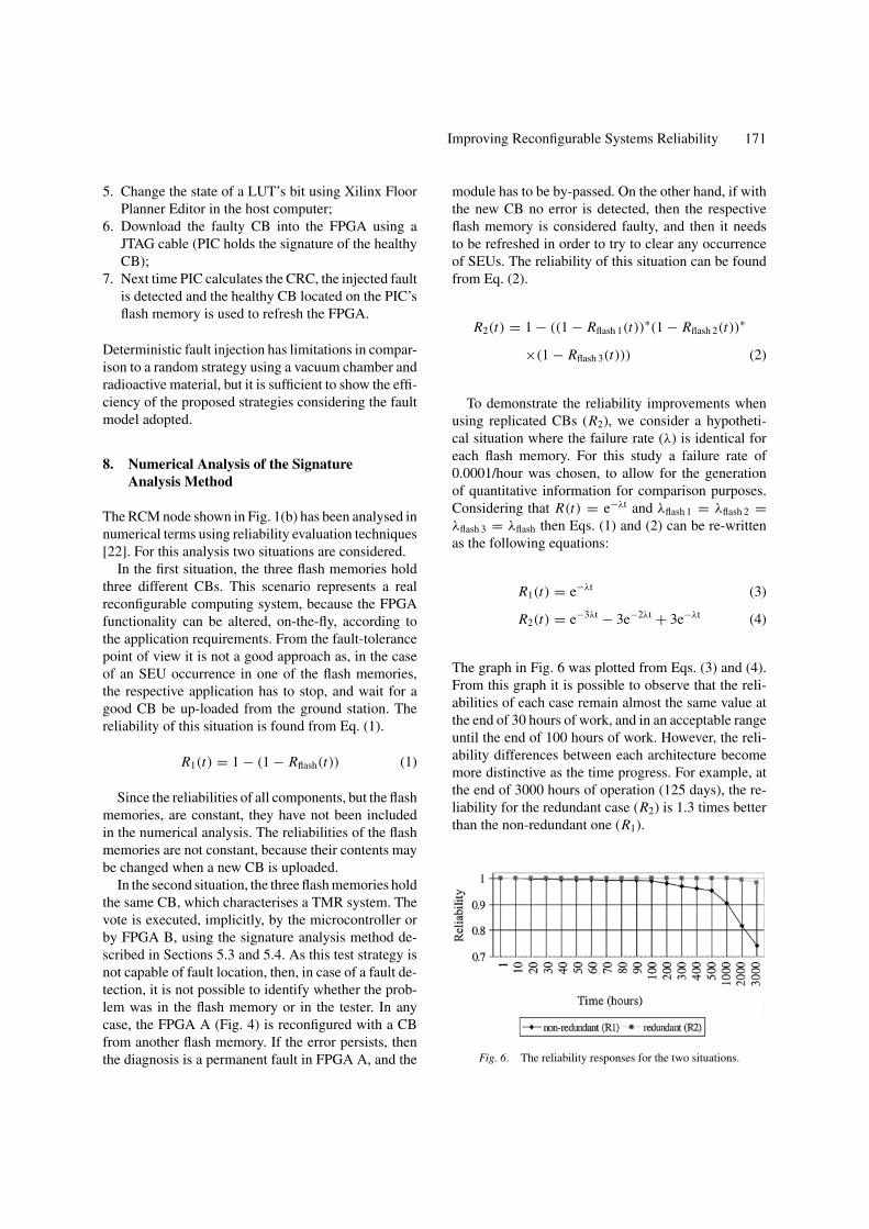
To demonstrate the reliability improvements whenusing replicated CBs (R2), we consider a hypotheti-cal situation where the failure rate (λ) is identical foreach flash memory. For this study a failure rate of0.0001/hour was chosen, to allow for the generationof quantitative information for comparison purposes.Considering that R(t) = e−λt and λflash 1 = λflash 2 =λflash 3 = λflash then Eqs. (1) and (2) can be re-writtenas the following equations:
R1(t) = e−λt (3)
R2(t) = e−3λt − 3e−2λt + 3e−λt (4)
The graph in Fig. 6 was plotted from Eqs. (3) and (4).From this graph it is possible to observe that the reli-abilities of each case remain almost the same value atthe end of 30 hours of work, and in an acceptable rangeuntil the end of 100 hours of work. However, the reli-ability differences between each architecture becomemore distinctive as the time progress. For example, atthe end of 3000 hours of operation (125 days), the re-liability for the redundant case (R2) is 1.3 times betterthan the non-redundant one (R1).
Fig. 6. The reliability responses for the two situations.

172 Bezerra, Vargas and Gough
9. Final Considerations
The design of reconfigurable computer systems, forspace applications, using SRAM-based FPGAs, de-pends not only on high reliability military devices be-ing available commercially, but also on the definitionof strategies for fault tolerance and on-board testing.
This work introduced the use of Built-In SelfTest (BIST) techniques and traditional fault-tolerancestrategies together with reconfigurable computing tech-nology, in order to improve some dependability fea-tures of on-board computers used in space applications.
The proposed strategies are described inSections 5.2, 5.3, 5.4 and 6. The strategies adoptedfor our particular implementation are described in Sec-tions 5.3 and 6, FPGA module with only one FPGA. Toimplement the signature analysis methods, an externaltester is necessary. From the reliability point of view,an advantage of using an FPGA as a tester is that thewhole system, including the testing algorithms and theuser’s application could be implemented at the samelevel of abstraction and using the same description lan-guage. This facilitates the use of formal verificationmethods, improving the system reliability at the designstage. On the other hand, the tester FPGA is an extrasingle point of failure, and for this reason the secondstrategy described in Section 5.3 can be considered, inour case, as the one providing more reliability to thesystem.
Another reason for having selected that strategy isthe savings in the PCB area usage and power consump-tion, which are extremely important concerns whendesigning on-board computers for space applications.In some applications where power consumption is notcrucial, the strategy described in Section 5.4 provideshigher levels of reliability.
Performance figures as, for instance, FPGA area us-age are not presented in this paper because of the rapidadvances in the FPGA industry both at the hardware(FPGA internal organisation) and software (synthesistools) levels.
A comparison between the proposed strategy andprevious works in not straightforward. Most of thestrategies for testing FPGAs found in the literature,target the manufacturer’s side, where the objective isto locate the fault inside the FPGA. From the user’spoint of view this information is irrelevant. The fewworks targeting the user’s side have considerable dif-ferences to the proposed one, for instance, in the lowoverhead approach [15]. In that approach, the FPGA is
partitioned in tiles, and each tile has logic blocks usedas spares. It is an expensive approach in terms of FPGAarea usage, but it is more effective than our proposedstrategy in case of permanent faults. The strategies de-scribed in this paper deserve a deeper investigation,in order to be used in the design of an adaptive on-board instrument processing system, entirely based onreconfigurable technology. During the case study im-plementation, a series of problems related to the devel-opment of FPGA based systems arose. For instance, thesynthesis tools available for high-level languages (e.g.VHDL behavioural and Verilog) are still not efficient,and a VHDL developer has to follow strict rules to ob-tain good results [3, 12]. An FPGA configuration bit-stream generated from a high-level language is spaceconsuming, and represents a lower performer circuitwhen compared to one generated from schematic dia-grams or low level languages such as VHDL structural.
Another concern is the time necessary for ElectronicDesign Automation (EDA) tools to generate CBs. Intime critical systems, such as space applications, ef-fective development facilities are important because ofthe short time available for making remedial changes toa faulty application. In the past several missions weresaved as a result of the rapid problem identification,followed by the development of a solution, groundtests and timely transmission of the new software tothe spacecraft computer. In addition to the selection ofefficient EDA tools, another investigation to be done isrelated to the hardware description language subject.
The original design had only FPGAs (see FPGAmodule on Fig. 4), but the programming effort in VHDLnecessary to implement the physical layer of the net-work protocol, and the FPGAs reconfiguration man-agement was too high. A microcontroller has beenadded to the original design of the RCM node, inorder to facilitate the software development. At thispoint it is important to make clear that it is not a hard-ware/software co-design project. The two parts of thesystem are completely independent, with a very welldefined interface. The software part (microcontroller)is developed and tested considering the existence of twoexternal objects. On one side there is the object networkbus used by the microcontroller to transmit and receivebytes to/from the network. On the other side there is theobject FPGA module, which receives/transmits bytesfrom/to the microcontroller and also it is tested and re-freshed according to the strategies defined in this work.The hardware part, FPGA module, has the microcon-troller as an external object used to feed the module

Improving Reconfigurable Systems Reliability 173
with bytes from the network and to send bytes to thenetwork. The tests and reconfigurations performed arecompletely transparent to the FPGA module.
From the fault tolerance point of view, there are sev-eral single points of failure at the node level in theproposed system. However, fault tolerance strategiesat the network level can be used to identify and to iso-late faulty nodes, keeping the system working. Thesestrategies are the subject of a future work.
Acknowledgments
This research was partly supported by CNPq—Brazilian Council for the Development of Science andTechnology, and PUCRS—Pontific Catholic Univer-sity of Rio Grande do Sul, Brazil.
References
1. P. Alfke and R. Padovani, “Radiation Tolerance of High-DensityFPGAs,” Xilinx High Reliable Products, Internal Reports 1999,http://www.xilinx.com/products/hirel qml.htm.
2. K. Beauchamp and C. Yuen, Digital Methods for Signal Ana-lysis, New York: George Allen & Unwin, 1979.
3. E.A. Bezerra and M.P. Gough, “A Guide to Migrating from Mi-croprocessor to FPGA Coping with the Support Tools Limita-tions,” Microprocessors and Microsystems, vol. 23, no. 10, pp.561–572, March 2000.
4. E.A. Bezerra, F. Vargas, and M.P. Gough, “Merging BIST andConfigurable Computing Technology to Improve Availability inSpace Applications,” Proc. 1st IEEE Latin American Test Work-shop (LATW’00), March 2000, Rio de Janeiro, Brazil, pp. 146–151.
5. E.A. Bezerra, M.P. Gough, and A. Buckley, “A VHDL Imple-mentation of an On-board ACF Application Targeting FPGAs,”Proc. Military and Aerospace Applications of ProgrammableLogic Devices Conf. (MAPLD’99), 1999, The Johns HopkinsUniversity, USA, pp. 290–296.
6. ESA, “Packet Utilisation Standard, Issue l,” European SpaceAgency (ESA) PSS-07-0, Noordwijk, The Netherlands, 1992.
7. ESA, “Cluster: mission, payload and supporting activities,”European Space Agency (ESA) SP-1159, Noordwijk, TheNetherlands, 1993.
8. ESA, “Development of On-Board Embedded Real-TimeSystems—An Engineering Approach,” European Space Agency(ESA) STR-260, Noordwijk, The Netherlands, 1999.
9. A. Fukunaga, K. Hayworth, and A. Stoica, “Evolvable Hardwarefor Spacecraft Autonomy,” NASA JPL Technical Reports, Snow-mass, Colorado, USA, 1998. http://techreports.jpl.nasa.gov/.
10. M.P. Gough, “Particle Correlator Instruments in Space: Perfor-mance Limitations Successes, and the Future,” American Geo-physics Union, Santa Fe Chapman Conf., USA, 1995.
11. K. Huang and F. Lombardi, “An Approach to Testing Pro-grammable/Configurable Field Programmable Gate Arrays,”Proc. 1996 IEEE VLSI Test Symp., 1996, pp. 450–455.
12. IEEE, “Draft Standard For VHDL Register Transfer Level Syn-thesis,” IEEE, USA, 1998.
13. F. Kocan and D.G. Saab, “Dynamic Fault Diagnosis on Reconfig-urable Hardware,” Proc. ACM/SIGDA Design Automation Con-ference (DAC’99), 1999, New Orleans, Louisiana, pp. 389–395.
14. J. Lach, W.H. Mangione-Smith, and M. Potkonjak, “EfficientlySupporting Fault-Tolerance in FPGAs,” Proc. ACM/SIGDA Int.Symp. on Field Programmable Gate Arrays (FPGA’98), Feb.1998, Monterey, California, pp. 132–141.
15. J. Lach, W.H. Mangione Smith, and M. Potkonjak, “Low Over-head Fault-Tolerant FPGA Systems,” IEEE Trans. VLSI Systems,vol. 6, no. 2, pp. 212–221, 1998.
16. W. Lawrenz, CAN System Engineering—From Theory to Prac-tical Applications, New York: Springer-Verlag, 1997.
17. G. Lum and G. Vandenboom, “Single Event Effects Testing ofXilinx FPGAs,” Xilinx High Reliable Products, Internal Report,1999, http://www.xilinx.com/products/hirel qml.htm.
18. O. Mattias, M. Ohlsson, P. Dyreklev, K. Johansson, and P.Alfke, “Neutron Single Event Upsets in SRAM-Based FP-GAs,” Xilinx High Reliable Products, Internal Report, 1999,http://www.xilinx.com/products/hirel qml.htm.
19. W.H. Mangione-Smith, B. Hutchings, D. Andrews, A. DeHon,C. Ebeling, R. Hartenstein, O. Mencer, J. Morris, K. Palem,V.K. Prasanna, and H.A.E. Spaanenburg, “Seeking Solutions inConfigurable Computing,” Computer, vol. 30, no. 12, pp. 38–43,Dec. 1997.
20. N. Muscettola, P.P. Nayak, B. Pell, and B. Williams, “Re-mote Agent: To Boldly Go Where No AI System Has GoneBefore,” IJCAI’97—Japanese Conf. on Artificial Intelligence,1997, Nayoga, Japan, pp. 48–60.
21. W.W. Peterson and E.J. Weldon, Error Correcting Codes,Cambridge, MA: MIT Press, 1972.
22. D.K. Pradhan, Fault-Tolerant Computer System Design, NewYork: Prentice-Hall, 1996.
23. C. Stroud, E. Lee, and M. Abramoviei, “Bist-Based Diagnosticof FPGA Logic Blocks,” Proc. Int. Test Conference (ITC’97),Nov. 1997, Washington, DC, pp. 539–547.
24. F. Vargas and M. Nicolaidis, “SEU-Tolerant SRAM DesignBased on Current Monitoring,” Proc. Int. Symp. on Fault-Tolerant Computing (FTCS’94), June 1994, Austin, Texas, pp.106–115.
25. J. Villasenor et al., “Configurable Computing Solutions for Au-tomatic Target Recognition,” Proc. IEEE Workshop on FPGAsfor Custom Computing Machines, April 1996, Napa, CA, pp.70–79.
26. Xilinx, “The Programmable Logic Data Book,” Xilinx, San Jose,1999.
27. Xilinx, “Virtex Configuration and Readback,” Xilinx Applica-tion Note 138 (XAPP 138), San Jose, March 1999.
Eduardo Augusto Bezerra received his Electronic Engineeringdegree from USURJ, Rio de Janeiro (Brazil) in 1991, and his MScdegree in Computer Science from UFRGS, Porto Alegre (Brazil) in1996. Since 1985 he has been working on the design and implementa-tion of software and hardware for embedded systems, and since 1993he has been working with fault tolerance and parallel processing. In1995 he started working with HW/SW co-design and reconfigurablecomputing technology. Since 1996, he is a lecturer at the Facultyof Informatics, PUC-RS, Brazil. Currently, he is a PhD candidate inComputing and Electronic Engineering at the Space Science Centre,

174 Bezerra, Vargas and Gough
University of Sussex, UK. WWW: http://www.sussex.ac.uk/space-science/ http://www.sussex.ac.uk/∼tapu9; http://www.inf.pucrs.br/∼eduardob.
Fabian Vargas is an Electronic Engineer (PUCRS, Brazil, 1988),MSc in Computer Science (UFRGS, Brazil, 1991) and PhD inMicroelectronics (INPG, Grenoble, France, 1995). At present, is aprofessor at the Electrical Engineering Dept., PUCRS, Brazil, andthe Chair of IEEE-TTTC for Latin America. He also founded andchaired the 1st IEEE Latin American Test Workshop (LATW’2000).His main areas of interest are Design of fault tolerant ICs and sys-tems, Built-In Self Test (BIST), and HW/SW Codesign.
Michael Paul Gough received his BSc Honours in 1967, MSc in1968 from the University of Leicester, UK and PhD, in 1972, from
the University of Southampton, UK. He is a Fellow of the Instituteof Electrical Engineers, Fellow of the Royal Astronomical Society,a Chartered Engineer and presently holds the2 position of Profes-sor of Space Science at the University of Sussex (UK). He is aauthor or co-author of over a hundred papers published coveringa broad range of scientific topics within the disciplines of SpaceScience, Information Systems, Physics and Geophysics, including:Ionospheric Physics; Magnetospheric Physics; Astrophysics; Instru-ment Technology; Space Plasma Physics; Microprocessor Applica-tions; Fault-Tolerance; Parallel Computing; Neural Networks; FuzzyLogic; and Data Compression. He has been a PI or Co-I for instru-ments flown on a number of spacecraft: ESA GEOS I & GOES II;UOSAT-2; AMPTE-UKS; CRRES; MARS-96; ESA Cluster I & II;STS-46 & STS-75, and on a number of sounding rockets: AUN;CAESAR; E2B; Pulsaur; OEDIPUS-C; Latur; and Svalbard. WWW:http://www.sussex.ac.uk/space-science/.