Impact of alloy disorder on the band structure of compressively strained GaBi x As 1− x
10
Impact of alloy disorder on the band structure of compressively strained GaBi x As 1-x Muhammad Usman, 1, * Christopher A. Broderick, 1, 2 Zahida Batool, 3 Konstanze Hild, 3 Thomas J. C. Hosea, 3, 4 Stephen J. Sweeney, 3 and Eoin P. O’Reilly 1, 2 1 Tyndall National Institute, Lee Maltings, Dyke Parade, Cork, Ireland 2 Department of Physics, University College Cork, Cork, Ireland 3 Advanced Technology Institute and Department of Physics, University of Surrey, Guildford, Surrey, GU2 7XH, United Kingdom 4 Ibnu Sina Institute for Fundamental Science Studies, Universiti Teknologi Malaysia, Johor Bahru, Johor 81310, Malaysia The incorporation of bismuth (Bi) in GaAs results in a large reduction of the band gap energy (Eg ) accompanied with a large increase in the spin-orbit splitting energy (4SO), leading to the condition that 4SO >Eg which is anticipated to reduce so-called CHSH Auger recombination losses whereby the energy and momentum of a recombining electron-hole pair is given to a second hole which is excited into the spin-orbit band. We theoretically investigate the electronic structure of experimentally grown GaBixAs1-x samples on (100) GaAs substrates by directly comparing our data with room temperature photo-modulated reflectance (PR) measurements. Our atomistic theoretical calculations, in agreement with the PR measurements, confirm that Eg is equal to 4SO for x ≈ 9%. We then theoretically probe the inhomogeneous broadening of the interband transition energies as a function of the alloy disorder. The broadening associated with spin-split-off transitions arises from conventional alloy effects, while the behaviour of the heavy-hole transitions can be well described using a valence band-anticrossing model. We show that for the samples containing 8.5% and 10.4% Bi the difficulty in identifying a clear light-hole-related transition energy from the measured PR data is due to the significant broadening of the host matrix light-hole states as a result of the presence of a large number of Bi resonant states in the same energy range and disorder in the alloy. We further provide quantitative estimates of the impact of supercell size and the assumed random distribution of Bi atoms on the interband transition energies in GaBixAs1-x. Our calculations support a type-I band alignment at the GaBixAs1-x/GaAs interface, consistent with recent experimental findings. I. INTRODUCTION There is increasing interest in the highly mis- matched semiconductor alloy, GaBi x As 1-x , both from a fundamental perspective 1–4 and also because of its potential device applications. 5–8 When a small frac- tion of As is replaced by Bi in GaAs, the energy gap E g decreases rapidly, by ≈ 90 meV when 1% of As is replaced by Bi. In addition, photo-reflectance mea- surements show that the energy separation, Δ SO , be- tween the spin-split-off valence band and the valence band edge also increases rapidly with Bi composition. 9 This then leads to the situation in GaBi x As 1-x , where the spin-orbit-splitting energy can exceed the energy gap Δ SO ≥ E g for x & 9%. This is of significant po- tential benefit for telecomm lasers, because it could enable the suppression of the Auger recombination losses which dominate the threshold characteristics of GaInAsP and AlGaInAs lasers. 5,7,10 The strong band gap bowing in GaBi x As 1-x is sim- ilar to that observed in GaN x As 1-x , where E g de- creases by as much as 150 meV when 1% of As is re- placed by N. The band gap reduction in GaN x As 1-x has been well explained using a band-anticrossing (BAC) model. 11 It is well established that replac- ing a single As atom by N introduces a resonant de- fect level above the conduction band edge (CBE) in GaAs. 12,13 This occurs because N is considerably more electronegative and is also 40% smaller than As. The interaction between the resonant N states and the CBE of the host GaAs matrix then accounts for the observed rapid reduction in E g . It was proposed 14 , and later confirmed theoretically 2,15 that replacing As by Bi can introduce a similar BAC effect. Like N and As, Bi is also a group-V element, which lies be- low Sb in the periodic table. Bi is much larger than As, and is also less electronegative. It should there- fore be expected that any Bi-related resonant defect levels should lie in the valence band (VB) and that, if an anticrossing interaction occurs, it will occur be- tween the Bi-related defect levels and the valence band edge (VBE) of the GaAs matrix. Recent sp 3 s * tight- binding calculations which we have performed confirm the existence of such a band-anticrossing interaction, with the calculated variation of E g and of Δ SO in ex- cellent agreement with experiment. 2 Although the BAC model provides an accurate de- scription of some of the key features in the band struc- ture of highly mismatched alloys, it includes several critical simplifying assumptions. It assumes for in- stance in GaBi x As 1-x that each Bi atom introduces resonant defect levels with constant energy E Bi , and then treats the effect on the band structure in terms of the interaction between these states and the host matrix valence band. The BAC model therefore effec- tively assumes that all Bi atoms are in an identical en- vironment. Although this may be approximately true for very low Bi compositions, where most Bi atoms are widely separated from each other, this assumption can be expected to break down with increasing Bi compo- sition. Firstly, there should be an increasing number of Bi pairs and clusters formed with increasing Bi com- position, where a Bi pair consists of a Ga atom that has two Bi neighbours, with clusters then containing larger numbers of contiguous Bi atoms. These pairs and clusters introduce defect levels which lie above the arXiv:1303.1070v1 [cond-mat.mtrl-sci] 5 Mar 2013
-
Upload
independent -
Category
Documents
-
view
0 -
download
0
Transcript of Impact of alloy disorder on the band structure of compressively strained GaBi x As 1− x
Impact of alloy disorder on the band structure of compressively strainedGaBixAs1−x
Muhammad Usman,1, ∗ Christopher A. Broderick,1, 2 Zahida Batool,3 Konstanze
Hild,3 Thomas J. C. Hosea,3, 4 Stephen J. Sweeney,3 and Eoin P. O’Reilly1, 2
1Tyndall National Institute, Lee Maltings, Dyke Parade, Cork, Ireland2Department of Physics, University College Cork, Cork, Ireland
3Advanced Technology Institute and Department of Physics,University of Surrey, Guildford, Surrey, GU2 7XH, United Kingdom
4Ibnu Sina Institute for Fundamental Science Studies,Universiti Teknologi Malaysia, Johor Bahru, Johor 81310, Malaysia
The incorporation of bismuth (Bi) in GaAs results in a large reduction of the band gap energy(Eg) accompanied with a large increase in the spin-orbit splitting energy (4SO), leading to thecondition that 4SO > Eg which is anticipated to reduce so-called CHSH Auger recombinationlosses whereby the energy and momentum of a recombining electron-hole pair is given to a secondhole which is excited into the spin-orbit band. We theoretically investigate the electronic structure ofexperimentally grown GaBixAs1−x samples on (100) GaAs substrates by directly comparing our datawith room temperature photo-modulated reflectance (PR) measurements. Our atomistic theoreticalcalculations, in agreement with the PR measurements, confirm that Eg is equal to 4SO for x ≈ 9%.We then theoretically probe the inhomogeneous broadening of the interband transition energies as afunction of the alloy disorder. The broadening associated with spin-split-off transitions arises fromconventional alloy effects, while the behaviour of the heavy-hole transitions can be well describedusing a valence band-anticrossing model. We show that for the samples containing 8.5% and 10.4%Bi the difficulty in identifying a clear light-hole-related transition energy from the measured PR datais due to the significant broadening of the host matrix light-hole states as a result of the presence ofa large number of Bi resonant states in the same energy range and disorder in the alloy. We furtherprovide quantitative estimates of the impact of supercell size and the assumed random distributionof Bi atoms on the interband transition energies in GaBixAs1−x. Our calculations support a type-Iband alignment at the GaBixAs1−x/GaAs interface, consistent with recent experimental findings.
I. INTRODUCTION
There is increasing interest in the highly mis-matched semiconductor alloy, GaBixAs1−x, both froma fundamental perspective1–4 and also because of itspotential device applications.5–8 When a small frac-tion of As is replaced by Bi in GaAs, the energy gapEg decreases rapidly, by ≈ 90 meV when 1% of Asis replaced by Bi. In addition, photo-reflectance mea-surements show that the energy separation, ∆SO, be-tween the spin-split-off valence band and the valenceband edge also increases rapidly with Bi composition.9
This then leads to the situation in GaBixAs1−x, wherethe spin-orbit-splitting energy can exceed the energygap ∆SO ≥ Eg for x & 9%. This is of significant po-tential benefit for telecomm lasers, because it couldenable the suppression of the Auger recombinationlosses which dominate the threshold characteristics ofGaInAsP and AlGaInAs lasers.5,7,10
The strong band gap bowing in GaBixAs1−x is sim-ilar to that observed in GaNxAs1−x, where Eg de-creases by as much as 150 meV when 1% of As is re-placed by N. The band gap reduction in GaNxAs1−xhas been well explained using a band-anticrossing(BAC) model.11 It is well established that replac-ing a single As atom by N introduces a resonant de-fect level above the conduction band edge (CBE) inGaAs.12,13 This occurs because N is considerably moreelectronegative and is also 40% smaller than As. Theinteraction between the resonant N states and theCBE of the host GaAs matrix then accounts for theobserved rapid reduction in Eg. It was proposed14,and later confirmed theoretically2,15 that replacing As
by Bi can introduce a similar BAC effect. Like Nand As, Bi is also a group-V element, which lies be-low Sb in the periodic table. Bi is much larger thanAs, and is also less electronegative. It should there-fore be expected that any Bi-related resonant defectlevels should lie in the valence band (VB) and that,if an anticrossing interaction occurs, it will occur be-tween the Bi-related defect levels and the valence bandedge (VBE) of the GaAs matrix. Recent sp3s∗ tight-binding calculations which we have performed confirmthe existence of such a band-anticrossing interaction,with the calculated variation of Eg and of ∆SO in ex-cellent agreement with experiment.2
Although the BAC model provides an accurate de-scription of some of the key features in the band struc-ture of highly mismatched alloys, it includes severalcritical simplifying assumptions. It assumes for in-stance in GaBixAs1−x that each Bi atom introducesresonant defect levels with constant energy EBi, andthen treats the effect on the band structure in termsof the interaction between these states and the hostmatrix valence band. The BAC model therefore effec-tively assumes that all Bi atoms are in an identical en-vironment. Although this may be approximately truefor very low Bi compositions, where most Bi atoms arewidely separated from each other, this assumption canbe expected to break down with increasing Bi compo-sition. Firstly, there should be an increasing numberof Bi pairs and clusters formed with increasing Bi com-position, where a Bi pair consists of a Ga atom thathas two Bi neighbours, with clusters then containinglarger numbers of contiguous Bi atoms. These pairsand clusters introduce defect levels which lie above the
arX
iv:1
303.
1070
v1 [
cond
-mat
.mtr
l-sc
i] 5
Mar
201
3
2
isolated Bi state energy, EBi and which also interactwith the valence band states2. In addition, isolated Biatoms also see an increasingly disordered local envi-ronment, leading to an inhomogeneous broadening ofthe associated resonant defect level energies. We in-vestigate here the effects of these two different types ofdisorder on the valence band structure of GaBixAs1−xgrown pseudomorphically on GaAs, using the sp3s∗
tight-binding model introduced in Ref. 2.
This paper presents a combined theoretical and ex-perimental analysis of the effects of disorder on theelectronic structure of GaBixAs1−x epilayers grownunder compressive strain on (100) GaAs substrates.Such layers are of interest for a number of reasons.Firstly, many applications such as semiconductorlasers and related devices require the growth of suchlayers. Secondly, the growth of these strained struc-tures has an interesting impact on the band structure,splitting the degeneracy of the heavy-hole and light-hole states at the valence band maximum, with thesplitting between the two sets of states initially in-creasing for instance at a rate of about ≈ 75 meV per% lattice mismatch for a compressively strained In-GaAs layer grown pseudomorphically on GaAs. Wenote that the compressive strain in a GaBixAs1−xpseudomorphic layer should also split the four-fold de-generacy of the Bi resonant states, with the two stateswith heavy-hole symmetry shifting upwards in energy,while the light-hole states shift downwards. With in-creasing strain, the GaAs host matrix light-hole statesshould start to pass through the Bi heavy-hole-like res-onant states. The intrinsic disorder in GaBiAs thenlead to mixing between these two types of state.
The GaBixAs1−x samples studied were grown bymolecular beam epitaxy with Bi concentrations ofx = 2.3%, 4.5%, 8.5%, and 10.4%.9,16,17 The sam-ples are fully strained (pseudomorphic) to the GaAssubstrate, as confirmed by x-ray diffraction data in-dicating the GaAs in-plane lattice constant for theGaBixAs1−x layers.16–18 The theoretical analysis wasundertaken using the sp3s∗ tight-binding Hamilto-nian which we have developed for GaBiAs2 to investi-gate the electronic structure of large randomly disor-dered supercells. The electronic structure is studiedexperimentally by photo-modulated reflectance (PR)spectroscopy9, which is considered to be an excellenttechnique due to its sensitivity to critical point tran-sitions in the band structure.19 Further details of theexperimental procedure are described in Batool et al.9,while the sample details can be found in Lu et al.16,17
Three sets of features are found in the PR spectra,associated with transitions between the conductionband minimum at Γ and valence states which respec-tively include host matrix heavy-hole (HH), light-hole(LH) and spin-split-off (SO) character. Our calcula-tions provide a detailed understanding of the broad-ening observed in the PR measurements for each ofthese features due to the presence not just of isolatedBi atoms but also of pair and cluster states. We finddifferent factors affecting each of the three transitions,with the calculated data being in generally good agree-ment with the measured spectra. In order to test theeffects of disorder, we undertake a set of supercell cal-
culations for each of the 4 samples investigated, wherethe supercell size is varied from 1000 to 8000 atoms,with several calculations with different random distri-butions of Bi atoms being undertaken for each super-cell size. We find for each supercell size that the cal-culated value of the energy gap separating the lowestconduction and highest (HH-like) valence states variesfor a given Bi composition x depending on the actualdistribution of Bi pair and cluster states in the su-percell considered, consistent with the inhomogeneousbroadening of the lowest energy transition in the PRspectra. The calculated transition energy to the SOband is largely independent of the supercell size andconfiguration, but we find that the GaAs host matrixSO state character is spread over a number of supercellstates, contributing also to an inhomogeneous broad-ening of the transition energy, which increases withincreasing Bi composition x. Finally we consider tran-sitions to states which include GaAs LH zone-centrecharacter. Because these states become degeneratewith a broad distribution of Bi-related resonant statesin a strained layer, we find that transitions to the LHstates become very strongly perturbed with increasingBi composition, with the GaAs LH Γ character distri-bution varying both with supercell size and with theparticular random distribution of Bi compositions. Athigher Bi compositions, no single feature can be asso-ciated with the GaAs LH states, consistent with thedifficulty in fully fitting the LH part of the spectrumat higher Bi compositions.
The remainder of the paper is organised as follows.We give a brief overview of the theoretical and ex-perimental methodology in section II. The main re-sults are then presented in section III. We begin bypresenting a general comparison between the exper-imental and theoretical results in section III A. Thisis followed in section III B by a more detailed anal-ysis of the effect of supercell size and of assumed Biatom distribution on the calculated spectra. We con-sider supercell sizes of 1000, 4096, and 8000 atoms foreach of the four grown samples. We find for a fixedBi composition that a larger supercell size results inan enhanced inhomogeneous broadening in particularof the LH character. The results clearly highlight theimportance of performing large supercell calculationsto model realistic dilute alloy environments. In sec-tion III C, we quantify the impact of the random dis-tribution of Bi atoms on the broadening of transitionenergies by performing 8000 atom supercell calcula-tions with four different random distributions of Biatoms for each of the four compositions considered.Our results indicate a significant broadening of thetransition energies due to the random distribution ofatoms, showing that the local band edge energies in aGaBiAs alloy are very sensitive to the Bi distributionin the given region. In section III D, we summarisethe key physical insights gained by comparison of ouratomistic simulations with the measured PR spectra.In section III E, we consider the band edge alignmentin compressively strained GaBixAs1−x/GaAs samples.The band alignment at the GaBixAs1−x/GaAs inter-face remains uncertain in the literature with reportssuggesting that the conduction band offset is of type

3
I,2,20,21 or type II,14 or nearly flat.22 Our calculationssupport a type-I band alignment for all the samplesconsidered. The overall conclusions of our work aresummarised in section IV.
II. METHODOLOGY
The atomistic calculations are performed using atight-binding (TB) model, where the alloy atom posi-tions are determined using a valence force field (VFF)strain energy minimization scheme and the electronicstructure is then calculated using an sp3s∗ TB Hamil-tonian, including bond-length and bond-angle depen-dent interaction parameters. The VFF and TB mod-els are implemented in NanoElectronic MOdeling Sim-ulator (NEMO 3-D).23,24 The values of the tight-binding parameters for GaAs and GaBi, as well as thevalues of the force constants (α and β) for the VFFmodel are reported in Ref. 2. The VFF parameters forGaBi were obtained by fitting to first principle calcula-tions of GaBi elastic constants.25 We further verified2
that the relaxed Ga-Bi bond lengths in GaBiAs cal-culated using the VFF model were in good agreementwith the results of the x-ray absorption spectroscopymeasurements,26 thereby confirming the validity ofthe VFF mdoel employed. The TB and VFF modelshave previously been applied to study free-standingGaBixAs1−x and GaBixP1−x supercells containing upto 8000 atoms. These calculations showed that Bi-related resonant states interact with GaAs host ma-trix valence band states in GaBixAs1−x via a composi-tion dependent band anti-crossing (BAC) interaction,which we calculate to shift the highest valence bandedge upwards in energy by ≈ 55 meV per % of Bireplacing As for low Bi compositions. This BAC in-teraction is analogous to the BAC interaction betweennitrogen (N) defect states and GaAs conduction bandstates in GaNxAs1−x alloys.27 The calculated compo-sitional dependence of the band gap and spin-orbit-splitting energies demonstrated excellent agreementwith the available experimental data sets includingBi samples with compositions up to 10%. The ex-perimentally observed large bowing of the band gapenergy was explained in terms of two factors: (i) alinear decrease of ≈ 30 meV per % Bi in the lowestconduction band edge energy (Ec1) which occurs dueto a conventional alloy shift and (ii) a large non-linearincrease in the highest valence band edge energy (Ev1)of ≈ 30-55 meV per % Bi due to the band anti-crossinginteraction. The energy of the spin-split-off band (SO)was calculated to shift downwards in energy slightly,exhibiting a linear decrease of ≈ 5 meV per % Bi. Itshould be noted that no evidence was found for anyBAC interaction involving the SO band, as earlier as-sumed by Alberi et al.14
In this paper, we apply our TB model to investigatecompressively strained GaBixAs1−x samples, grownepitaxially on a (100) GaAs substrate. In the VFFrelaxation scheme, we keep the in-plane lattice con-stant for all supercells considered fixed to that of theGaAs lattice constant, while allowing the supercell torelax freely along the growth direction. We use peri-
odic boundary conditions in all three spatial directionsfor the calculations of electronic structure. For eachcalculation undertaken, the Bi atoms are placed on Assites, selected randomly in the supercells.
In order to compare the theoretical calculationswith the experimental data, we calculate the distri-bution of the host matrix Γ-character, GΓ(E), acrossthe alloy valence band states. The calculation of theΓ-character is carried out by projection of the six high-est host matrix zone centre valence band states (twoHH, two LH and two SO) onto the full spectrum ofthe energy states in the alloy (GaBixAs1−x) supercellunder consideration. In what follows, we use the sub-scripts l, 0 and k, 1 to index the unperturbed host andBi-containing alloy states, respectively. The GΓ(E)spectrum is then calculated by projecting the unper-turbed GaMAsM supercell states at Γ, |ψl,0〉, ontothe spectrum of the GaMBiLAsM−L alloy supercell,{Ek, |ψk,1〉}:
GΓ (E) =∑k
g(El)∑l=1
fΓ,kl δ (Ek − E) (1)
fΓ,kl = |〈ψk,1|ψl,0〉|2 (2)
Here δ (Ek − E) is the Dirac delta function centredon Ek, g(El) is the degeneracy of the host matrixband having energy El at the Γ point in the Brillouinzone and
∑l fΓ,kl is the fractional Γ character of the
alloy state |ψk,1〉. Since the PR measurements areperformed at room temperature (300 K) and the TBcalculations are parametrised to the low temperatureband structure, we shift the energy scale of our theo-retically calculated Γ-character plots at 0 K by 0.098eV to convert them to room temperature values.
The analysis of GΓ(E) plots has provided a veryuseful approach to understand the character and evo-lution of alloy band edge states.2,27 Analysis of suchplots confirms the presence of the band anti-crossinginteraction in ordered supercell calculations of dilutebismide alloys.28
Turning to the experimental data, the measuredPR spectral line shapes were least-squares fitted usingAspnes third derivative functionals of the form29:
4RR
= Re[Ceiθ (E − Eg + iγ)−n
] (3)
where C and θ are amplitude and phase variables, Ethe energy of the probe beam, Eg the critical pointtransition energy, and γ a broadening parameter. Weinvestigated the effect of choosing several of the sug-gested values for the line shape exponent factor n,29
but found that this had little influence on the fittedtransition energies. Here, we present the results forfits using n = 3. In the next section III A, we useEq. 3 to fit the measured PR data and identify theinterband transition energies.
4
TABLE I: The values of the broadening parameters γ used in Eq. 3 to fit the PR spectra plotted in Figs. 1 and 2.
Bi composition γHH γLH γSO
(%) (meV) (meV) (meV)2.3 82.1 ± 5.3 51.9 ± 3.5 30.9 ± 0.34.5 31.3 ± 1.2 31.0 ± 2.0 22.2 ± 1.38.5 31.4 ± 0.5 82.1 ± 7.0 31.9 ± 2.210.4 31.4 ± 1.0 31.4 ± 1.0∗ 38.4 ± 3.2
*Here γLH was constrained to equal γHH in thefit for 10.4% Bi, due to an extra feature in theLH energy range which is difficult to model.
III. RESULTS AND DISCUSSIONS
A. Comparison of Theory and Experiment
Fig. 1 shows the measured PR spectra (black dots)near to and just above the energy gap for the fourGaBixAs1−x samples considered, with compositions x= 2.3%, 4.5%, 8.5%, and 10.4%. The measured PRdata have been fitted using Eq. 3, with the fits shownin the figure by the solid red lines. The values ofthe broadening parameter γ used in Eq. 3 to obtainbest fits to the experimental data are listed in tableI. These values are directly related both to inhomo-geneous broadening of the transition energies due toalloy disorder effects in the grown samples, as wellas to any composition fluctuation effects. The fittedγ values will be compared to the broadening of ourtheoretically calculated Γ-character plots later in thispaper.
For each composition case shown in Fig. 1, cumu-lative HH+LH Γ character spectra are also plotted,using the same energy scale (green bars) and whereeach peak in the theoretical spectra is associated witha transition between the lowest conduction state anda given valence state. The Γ-character plots are com-puted from 8000 atom supercell calculations, with theBi atoms randomly distributed within each supercellconsidered. Here we consider only one random distri-bution of Bi atoms to compare against experiment foreach composition. The results here therefore highlightalloy disorder effects such as mixing of alloy valenceband states with Bi pair and cluster related states,as a function of the Bi composition. Later in sectionIII C, we will investigate the second important factorthat contributes in the inhomogeneous broadening ofthe transition energies by performing calculations forfour different random distributions of Bi atoms foreach grown sample. These later results will show thatthe specific distribution of Bi atoms within a super-cell can further alter the calculated energy spectra byintroducing different Bi local environments. This canresult in a redistribution of Γ-character and shifts inthe transition energies, thus providing a further con-tribution to the inhomogeneous broadening of the cal-culated spectra.
We find that the alloy conduction band (CB) Γ-character is largely concentrated on the lowest energyconduction state of the alloy, which retains more than95% Γ character for all of the supercells and Bi compo-
0.6 0.7 0.8 0.9 1.0 1.1 1.2 1.3 1.4 1.5 1.6 1.7Energy (eV)
// //
////
// //
0.5
0
-0.5
1.5
1.0
0.5
2.22.01.81.61.4
3.5
3.0
2.5
2.0
∆R
/R (1
0
)-4
x4
x20
x2
Bi = 2.3%
Bi = 4.5%
Bi = 8.5%
Bi = 10.4%
EgEv1
EgEv2
Fraction
al HH
+LH
Γ Ch
aracter
1.0
0.5
0
1.0
0.5
0
1.0
0.5
0
1.0
0.5
0
Broadening of LH transition energy
(a)
(b)
(c)
(d)
FIG. 1: Room temperature photo-reflectance (PR) spectrafor the four compressively-strained GaBixAs1−x samples,in the region of the fundamental band gap highlightingthe EEv1
g = Ec1− Ev1 and EEv2g = Ec1− Ev2 transitions.
The black circles are from measured values and the redlines are the fits obtained by equation 3. The green barsare the calculated GaAs HH+LH Γ-character plots for thealloy valence band states, computed from 8000 atom su-percell calculations. The values of the HH and LH relatedtransition energies are selected from the Γ character plotsas the energies with the highest HH and LH Γ characterprojections, respectively. The dashed lines are a guide tothe eye and indicate the PR fitting transition energies.
sitions considered. This is consistent with our previ-ous free-standing GaBixAs1−x supercell calculations,where the conduction band Γ-character was found tobe more than 99.9% concentrated on the lowest energystate.2 This confirms that we can use a conventionalalloy model to describe the shift in the conductionband edge energy with alloy composition. Therefore,we do not show plots of the CB Γ-character in thispaper, and use the calculated lowest conduction bandedge energy, Ec1, to compute the interband transitionenergies.
The two composition dependent features in the PRplots of Fig. 1 are assigned for the 2.3% and 4.5%samples to the EEv1
g = Ec1− Ev1 and EEv2g = Ec1−
Ev2 transitions. This assignment is supported by theΓ-character plots, where the lower energy feature isassociated with transitions to HH-like valence states(Ev1) and the higher energy feature with transitions
5
1.55 1.60 1.65 1.70 1.75 1.80 1.85Energy (eV)
(a) Bi = 2.3%
(b) Bi = 4.5%
(c) Bi = 8.5%
(d) Bi = 10.4%
x2
x5
0.5
0
-0.5
1.0
0.80.6
0.4
0.2
1.81.61.41.21.00.8
2.42.2
2.01.81.6
ΔR/
R (1
0 )
-4Eg
ESO
1.00.50
1.00.50
1.00.50
1.00.50
Fractional Γ HH
/LH C
haracter
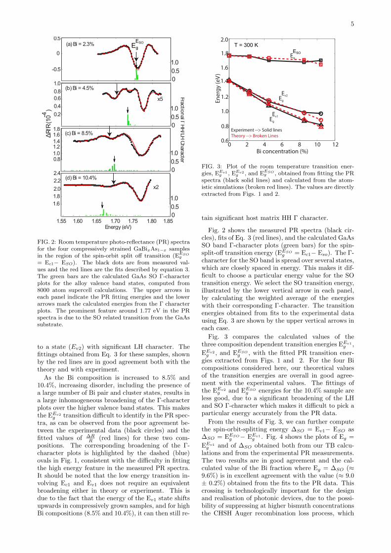
FIG. 2: Room temperature photo-reflectance (PR) spectrafor the four compressively strained GaBixAs1−x samplesin the region of the spin-orbit split off transition (EESO
g
= Ec1− ESO). The black dots are from measured val-ues and the red lines are the fits described by equation 3.The green bars are the calculated GaAs SO Γ-characterplots for the alloy valence band states, computed from8000 atom supercell calculations. The upper arrows ineach panel indicate the PR fitting energies and the lowerarrows mark the calculated energies from the Γ characterplots. The prominent feature around 1.77 eV in the PRspectra is due to the SO related transition from the GaAssubstrate.
to a state (Ev2) with significant LH character. Thefittings obtained from Eq. 3 for these samples, shownby the red lines are in good agreement both with thetheory and with experiment.
As the Bi composition is increased to 8.5% and10.4%, increasing disorder, including the presence ofa large number of Bi pair and cluster states, results ina large inhomogeneous broadening of the Γ-characterplots over the higher valence band states. This makesthe EEv2
g transition difficult to identify in the PR spec-tra, as can be observed from the poor agreement be-tween the experimental data (black circles) and thefitted values of ∆R
R (red lines) for these two com-positions. The corresponding broadening of the Γ-character plots is highlighted by the dashed (blue)ovals in Fig. 1, consistent with the difficulty in fittingthe high energy feature in the measured PR spectra.It should be noted that the low energy transition in-volving Ec1 and Ev1 does not require an equivalentbroadening either in theory or experiment. This isdue to the fact that the energy of the Ev1 state shiftsupwards in compressively grown samples, and for highBi compositions (8.5% and 10.4%), it can then still re-
0 2 4 6 8 10 12
2.0
1.8
1.6
1.4
1.2
1.0
0.8
0.6
Bi concentration (%)
Ene
rgy
(eV
)
Eg
Eg
Ev1
Eg
Ev2
Experiment --> Solid lines
ESO
Theory --> Broken Lines
T = 300 K
FIG. 3: Plot of the room temperature transition ener-gies, EEv1
g , EEv2g , and EESO
g , obtained from fitting the PRspectra (black solid lines) and calculated from the atom-istic simulations (broken red lines). The values are directlyextracted from Figs. 1 and 2.
tain significant host matrix HH Γ character.
Fig. 2 shows the measured PR spectra (black cir-cles), fits of Eq. 3 (red lines), and the calculated GaAsSO band Γ-character plots (green bars) for the spin-split-off transition energy (EESO
g = Ec1− Eso). The Γ-character for the SO band is spread over several states,which are closely spaced in energy. This makes it dif-ficult to choose a particular energy value for the SOtransition energy. We select the SO transition energy,illustrated by the lower vertical arrow in each panel,by calculating the weighted average of the energieswith their corresponding Γ-character. The transitionenergies obtained from fits to the experimental datausing Eq. 3 are shown by the upper vertical arrows ineach case.
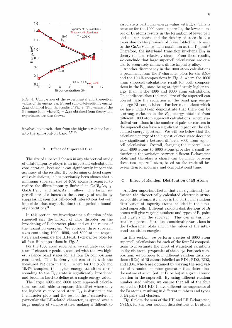
Fig. 3 compares the calculated values of thethree composition dependent transition energies EEv1
g ,
EEv2g , and EESO
g , with the fitted PR transition ener-gies extracted from Figs. 1 and 2. For the four Bicompositions considered here, our theoretical valuesof the transition energies are overall in good agree-ment with the experimental values. The fittings ofthe EEv2
g and EESOg energies for the 10.4% sample are
less good, due to a significant broadening of the LHand SO Γ-character which makes it difficult to pick aparticular energy accurately from the PR data.
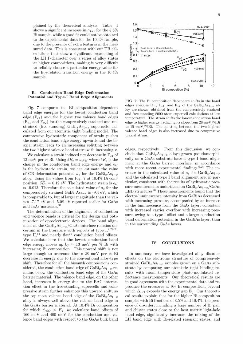
From the results of Fig. 3, we can further computethe spin-orbit-splitting energy ∆SO = Ev1− ESO as∆SO = EESO
g − EEv1g . Fig. 4 shows the plots of Eg =
EEv1g and of ∆SO obtained both from our TB calcu-
lations and from the experimental PR measurements.The two results are in good agreement and the cal-culated value of the Bi fraction where Eg = ∆SO (≈9.6%) is in excellent agreement with the value (≈ 9.0± 0.2%) obtained from the fits to the PR data. Thiscrossing is technologically important for the designand realisation of photonic devices, due to the possi-bility of suppressing at higher bismuth concentrationsthe CHSH Auger recombination loss process, which
6
Experiment --> Solid linesTheory --> Broken Lines
EgEv1
ΔSO
0 2 4 6 8 10 12 Bi concentration (%)
0.2
0.4
1.6
1.4
1.2
1.0
0.8
0.6
Ene
rgy
(eV
)
9.0 +/- 0.2 % ~9.6%
T = 300 K
FIG. 4: Comparison of the experimental and theoreticalvalues of the energy gap Eg and spin-orbit-splitting energy∆SO obtained from the results of Fig. 3. The values of theBi composition where Eg = ∆SO obtained from theory andexperiment are also shown.
involves hole excitation from the highest valence bandinto the spin-split-off band.5,7,10
B. Effect of Supercell Size
The size of supercell chosen in any theoretical studyof dilute impurity alloys is an important calculationalconsideration, because it can significantly impact theaccuracy of the results. By performing ordered super-cell calculations, it has previously been shown that aminimum supercell size of 4096 atoms is required torealize the dilute impurity limit2,15 in GaBixAs1−x,GaBixP1−x, and InBixAs1−x alloys. The larger su-percell size also increases the accuracy of results bysuppressing spurious cell-to-cell interactions betweenimpurities that may arise due to the periodic bound-ary conditions.30
In this section, we investigate as a function of thesupercell size the impact of alloy disorder on thebroadening of Γ-character plots and on the values ofthe transition energies. We consider three supercellsizes containing 1000, 4096, and 8000 atoms respec-tively and compare the HH+LH Γ-character plots forall four Bi compositions in Fig. 5.
For the 1000 atom supercells, we calculate two dis-tinct Γ-character peaks associated with the two high-est valence band states for all four Bi compositionsconsidered. This is clearly not consistent with themeasured PR data in Fig. 1, where for the 8.5% and10.4% samples, the higher energy transition corre-sponding to the Ev2 state is significantly broadenedand becomes hard to define at a single energy value.
The larger 4096 and 8000 atom supercell calcula-tions are both able to capture this effect where onlythe highest valence band state Ev1 is distinct in theΓ-character plots and the rest of the Γ-character, inparticular the LH-related character, is spread over alarge number of valence states, making it difficult to
associate a particular energy value with Ev2. This isbecause for the 1000 atom supercells, the lower num-ber of Bi atoms results in the formation of fewer pairand cluster states, and the density of states is alsolower due to the presence of fewer folded bands nearto the GaAs valence band maximum at the Γ point.2
Therefore, the interband transition involving Ev2 intheory remains relatively sharp. From these results,we conclude that large supercell calculations are cru-cial to accurately mimic a dilute impurity alloy.
Another discrepancy in the 1000 atom calculationsis prominent from the Γ character plots for the 8.5%and the 10.4% compositions in Fig. 5, where the 1000atom supercell calculations result for both composi-tions in the Ev1 state being at significantly higher en-ergy than in the 4096 and 8000 atom calculations.This indicates that the small size of the supercell canoverestimate the reduction in the band gap energyat large Bi compositions. Further calculations whichwe have undertaken demonstrate that there can bea strong variation in the Ev1 energy obtained fromdifferent 1000 atom supercell calculations, where sta-tistical variations in the number of pairs or clusters inthe supercell can have a significant impact on the cal-culated energy spectrum. We will see below that thecalculated energy of the highest valence state does notvary significantly between different 8000 atom super-cell calculations. Overall, changing the supercell sizefrom 4096 atoms to 8000 atoms provides a small re-duction in the variation between different Γ-characterplots and therefore a choice can be made betweenthese two supercell sizes, based on the trade-off be-tween desired accuracy and computational time.
C. Effect of Random Distribution of Bi Atoms
Another important factor that can significantly in-fluence the theoretically calculated electronic struc-ture of dilute impurity alloys is the particular randomdistribution of impurity atoms included in the simu-lated supercells. Different random distributions of Biatoms will give varying numbers and types of Bi pairsand clusters in the supercell. This can in turn forsmaller supercells introduce considerable variations inthe Γ-character plots and in the values of the inter-band transition energies.
In this section, we perform a series of 8000 atomsupercell calculations for each of the four Bi composi-tions to investigate the effect of statistical variationson the electronic properties of the alloy. For each com-position, we consider four different random distribu-tions (RDs) of Bi atoms labelled as RD1, RD2, RD3,and RD4, which are obtained by varying the seed val-ues of a random number generator that determinesthe nature of anion (either Bi or As) at a given atomiclocation in the supercell. By using different randomnumber seed values, we ensure that all of the foursupercells (RD1-RD4) have different arrangements ofthe Bi atoms, resulting in different numbers and typesof Bi pairs and clusters.
Fig. 6 plots the sum of the HH and LH Γ-character,GΓ(E), for the four random distributions of Bi atoms

7
FIG. 5: For each Bi composition of the experimentally grown samples, we calculate and plot combined HH and LH Γcharacter for three alloy supercells consisting of 1000, 4096, and 8000 atoms. For the same Bi composition, a larger alloysupercell will have more Bi atoms and therefore an increased number of pair and cluster configurations. This is reflectedby the wider Γ character distribution for larger supercells. The significant overestimation of the alloy VBE energy in1000 atom supercell calculations for 8.5% and 10.4% samples is due to artificially enhanced cell-to-cell interaction of pairand cluster states in the structures considered.
0 0.1 0.2 0.3 0.4 0.5Energy (eV)
00.5
1.00
0.5
1.00
0.5
1.0
00.5
1.0
HH
+LH
Γ C
har
acte
r
RD1
RD2
RD3
RD4
0 0.1 0.2 0.3 0.4 0.5Energy (eV)
00.5
1.00
0.5
1.00
0.5
1.0
00.5
1.0
HH
+LH
Γ C
har
acte
r
RD1
RD2
RD3
RD4(57,0.1)
(1,20)
(2,18)
(3,11)
(9,7)(18,4)(32,18)(9,30)
(5,6)
(50,3)(11,36)(6,25)
(2,6)
(65,2)(2,63)
(,3)(4,2)
(43,5)(8,27)(8,7)(5,14)
Bi = 2.3% Bi = 4.5%
Bi = 8.5% Bi = 10.4%
0 0.1 0.2 0.3 0.4 0.5Energy (eV)
00.5
1.00
0.5
1.00
0.5
1.0
00.5
1.0
HH
+LH
Γ C
har
acte
r
RD1
RD2
RD3
RD4
0 0.1 0.2 0.3 0.4 0.5Energy (eV)
00.5
1.00
0.5
1.00
0.5
1.0
00.5
1.0
HH
+LH
Γ C
har
acte
r
RD1
RD2
RD3
RD4
(55,0.2)(4,11)
(6,3)(,13)
(59,0.1)(4,1)(,5)
(,13)(3,8)
(52,0.7)(1,3)
(6,5)(4,4)(1,6)(,13)
(,8)
(61,0.2)(1,5)(,3)
(2,23)(,9)(,7)
(37,1)(20,10)(6,5)
(2,1)
(2,7)
(54,0.3)(,2)
(3,10)(3,15)
(64,0.1)(1,4)(2,21)
(,10)(,5)
(47,0.1)(13,2)(,8)(2,20)(,5)(,5)(,6)
(23,5)(32,9)(3,12)
(3,4)
(39,2)(13,12)
(8,12)
(,18)
(2,4)(3,10)
(15,4)(45,5)(1,34)
(3,2)(,6)(,5)(,7)
FIG. 6: For each of the four Bi compositions, we consider four random distributions of Bi atoms in the supercell, labelledas RD1, RD2, RD3, and RD4. Each random distribution introduces different pair and cluster states and thereforeexhibits different broadening of the combined HH and LH Γ-character. The calculated data are shown for 8000 atomsupercell calculations. We also specify the values of individual HH and LH contributions in the few highest energy barsof the plot as (HH,LH). If (,LH) or (HH,) is mentioned for a particular bar, that indicates that HH or LH contributionin that bar is less than 0.1%. The zero of energy is taken in all cases at the GaAs valence band maximum.

8
considered at each composition. We specify the sepa-rate contributions from the GaAs HH and LH statesin the label (HH,LH) for the highest few states, in or-der to highlight the distribution of the HH and LHcharacter over the alloy states. It should be notedthat (,LH) and (HH,) refers to cases where a particu-lar alloy state has less than 0.1% HH or LH character,respectively.
The impact of variations between different randomdistributions is more prominent for the two lower Bicompositions, 2.3% and 4.5%. This can be mainly at-tributed to two reasons: (i) For the lower Bi composi-tions, there is a significantly smaller number of pairsand clusters in a supercell, and therefore the impactof any variation in their type or number is more pro-nounced. Similar conclusions were presented earlier2
based on free-standing supercell calculations, wherethe addition of a single pair or a single Ga-centred3 Bi cluster in a 4096 atom Ga2048BiMAs2048−M su-percell (M=2, 3) resulted in very large variations inthe valence band edge energies. (ii) The highest va-lence band edge energy is very close to the energies ofthe pair/cluster states and the stronger state mixingwhich this allows therefore results in the broadened Γ-character distributions. This behaviour is confirmedby close examination of RD1 for 2.3% Bi and RD1 andRD3 for 4.6% Bi. These are the distributions whichgive rise to the highest valence band maximum ener-gies, and also have the lowest Γ character associatedwith the highest state, reflecting the contribution of(higher energy) pair or cluster states in each of thesecases. The large γHH value required to fit the PRspectrum of the 2.3% sample may then include a con-tribution due to mixing of the host Γ states with pairand cluster states which lie close to the band edge atthis composition.
For the larger Bi compositions, 8.5% and 10.4%, thehighest valence band edge energy increases well abovethe energies of the pair/cluster states and thereforea sharp peak is observed for Ev1 in the Γ-characterplots. This is quite evident for the 10.4% compositioncase, where 55%, 59%, 52%, and 61% HH character isfound on the highest valence band state for the fourrandom distributions. For these compositions, the LHΓ-character is in each case distributed over a broadrange of valence band states, so that it then provesvery difficult in the 10.4% cases to identify any singlestate as the LH-like valence band maximum, consis-tent with the difficulty in fitting the PR spectra inthis energy range.
D. Summary of the Alloy Disorder Effects andComparison with the PR fits
In the previous two subsections III B and III C, wehave investigated the calculated impact of alloy dis-order when varying two important parameters: su-percell size and the assumed (random) distributionof impurity atoms. Both of these factors have beenfound to significantly impact the calculated electronicstructure of GaBixAs1−x alloys, and therefore requirecareful attention. Below, we summarize our results
and the key physical insights gained in the previoussubsections concerning the electronic properties of thealloy:
• A very small supercell size can result in arti-ficially enhanced alloy disorder effects on theband edge energies, and can therefore introducesignificant errors in the calculated band gap en-ergy. Small supercells also fail to correctly cap-ture the broadening of LH character observedin experimental PR data for higher Bi compo-sitions. Our calculations show that a supercellsize of 4096 or larger is required to accuratelymodel dilute bismide alloys.
• The effect of atomistic randomness remains im-portant at low Bi compositions (2.3% and 4.5%)even in larger supercells, where variations in thelocal Bi environments can significantly impactthe calculated distribution of Γ-character, con-sistent with the large γHH value required to fitthe 2.3% PR spectrum.
• At higher Bi compositions (8.5% and 10.4%),the effect of atomistic randomness is less markedat the valence band maximum, because the Ev1
energy is shifted well above the pair/clusterstate energies.
• Overall, the broadening of the theoretically cal-culated Γ-character plots correlates well withthe values of the broadening parameter γ (pro-vided in table I) used to fit the PR spectravia Eq. 3. The large values of the γ parame-ter used to fit the PR data for the 2.3% sam-ple may include a contribution due to compo-sition variations in the grown sample, as wellas a contribution due to state mixing with pairand cluster states. For the three higher compo-sition samples, a constant value of γHH can bechosen to fit the HH-related transition. Thisis consistent with the theoretically computedΓ-character plots, where the HH-character islargely present on the alloy VBE state and doesnot show much spreading even for different ran-dom distributions of the Bi atoms, as evidentfrom the plots in Fig. 6.
• The value of the γSO broadening parameter intable I for the SO band slightly increases withBi composition. This is consistent with the Γ-character plots shown in Fig. 2, which show anincrease in broadening of the Γ-character withincreasing composition. In order to quantify thiseffect, we estimate the calculated broadening ofthe SO Γ character by calculating the energyrange 4E around ESO which includes 70% ofthe SO character. The values obtained for 2.3%,4.5%, 8.5%, and 10.4% Bi compositions are <1meV, 2.7 meV, 5.7 meV, and 13.8 meV, clearlyindicating an increasing broadening of SO Γ-character with increasing Bi composition, con-sistent with conventional alloy disorder effects.
• The behaviour of the γLH parameter values forthe LH-related transition energy is also well ex-
9
plained by the theoretical analysis. Table Ishows a significant increase in γLH for the 8.6%Bi sample, while a good fit could not be obtainedto the experimental data for the 10.4% sample,due to the presence of extra features in the mea-sured data. This is consistent with our TB cal-culations that show a significant broadening ofthe LH Γ-character over a series of alloy statesat higher compositions, making it very difficultto reliably choose a particular energy value forthe Ev2-related transition energy in the 10.4%sample.
E. Conduction Band Edge DeformationPotential and Type-I Band Edge Alignments
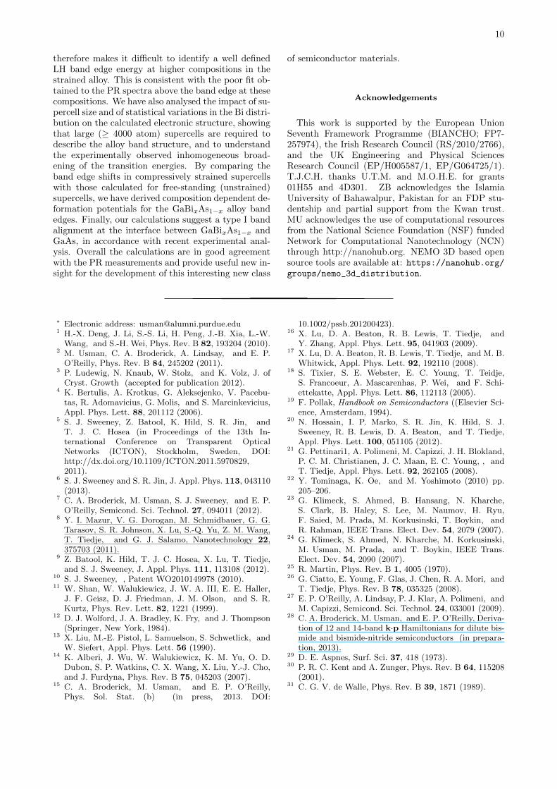
Fig. 7 compares the Bi composition dependentband edge energies for the lowest conduction bandedge (Ec1) and the highest two valence band edges(Ev1 and Ev2) for the compressively strained and un-strained (free-standing) GaBixAs1−x supercells, cal-culated from our atomistic tight binding model. Thecompressive hydrostatic component of strain pushesthe conduction band edge energy upwards and the bi-axial strain leads to an increasing splitting betweenthe two highest valence band states with increasing x.
We calculate a strain induced net decrease in Ec1 of13 meV per % Bi. Using δEc = acεH where δEc is thechange in the conduction band edge energy and εHis the hydrostatic strain, we can estimate the valueof CB deformation potential ac for the GaBixAs1−xalloy. Using the values from Fig. 7 at 10.4% Bi com-position, δEc = 0.12 eV. The hydrostatic strain is εH≈ -0.013. Therefore the calculated value of ac for thecompressively strained GaBixAs1−x is -9.4 eV, whichis comparable to, but of larger magnitude than the val-ues -7.17 eV and -5.08 eV reported earlier for GaAsand InAs materials.31
The determination of the alignment of conductionand valence bands is critical for the design and opti-mization of optoelectronic devices. The band align-ment at the GaBixAs1−x/GaAs interface remains un-certain in the literature with reports of type I,2,20,21
type II,14 and nearly flat22 conduction band offsets.We calculate here that the lowest conduction bandedge energy moves up by ≈ 13 meV per % Bi withincreasing Bi composition. This upward shift is notlarge enough to overcome the ≈ 28 meV per % Bidecrease in energy due to the conventional alloy-typeshift. Therefore for all the bismuth compositions con-sidered, the conduction band edge of GaBixAs1−x re-mains below the conduction band edge of the GaAsbarrier material. The valence band edge, on the otherhand, increases in energy due to the BAC interac-tion effect in the free-standing supercells and com-pressive strain further enhances this upward shift, sothe top most valence band edge of the GaBixAs1−xalloy is always well above the valence band edge inthe GaAs barrier material. At 10.4% Bi compositionfor which 4SO > Eg, we calculate band offsets of160 meV and 400 meV for the conduction and va-lence band edges with respect to the GaAs bulk band
1.6
1.5
1.4
1.3
1.2
Ene
rgy
(eV
)
// //0.4
0.3
0.2
0.1
0
Solid lines --> strained GaBiAsBroken lines --> unstrained GaBiAs
0 2 4 6 8 10 12Bi composition (%)
Ec1
Ev1
Ev2
GaAs VBE
GaAs CBE
T = 0K
158 meV
400 meV
FIG. 7: The Bi composition dependent shifts in the bandedges energies Ec1, Ev1, and Ev2 of the GaBixAs1−x al-loy are shown, obtained from the compressively strainedand free-standing 8000 atom supercell calculations at lowtemperature. The strain shifts the lowest conduction bandedge to higher energy, reducing its slope from 28 meV/%Bito 15 meV/%Bi. The splitting between the two highestvalence band edges is also increased due to compressivebiaxial strain.
edges, respectively. From this discussion, we con-clude that GaBixAs1−x alloys grown pseudomorphi-cally on a GaAs substrate have a type I band align-ment at the GaAs barrier interface, in accordancewith more recent experimental findings.9,20 The in-crease in the calculated value of ac for GaBixAs1−xand the calculated type I band alignment are, in par-ticular, consistent with the results of hydrostatic pres-sure measurements undertaken on GaBixAs1−x/GaAsLED structures20 These measurements found that theelectro-luminescence intensity from GaBiAs decreasedwith increasing pressure, accompanied by an increasein the luminescence from the GaAs layer, consistentwith increased carrier overflow with increasing pres-sure, owing to a type I offset and a larger conductionband deformation potential in the GaBiAs layer, thanin the surrounding GaAs layers.
IV. CONCLUSIONS
In summary, we have investigated alloy disordereffects on the electronic structure of compressivelystrained GaBixAs1−x samples grown on a GaAs sub-strate by comparing our atomistic tight binding re-sults with room temperature photo-modulated re-flectance measurements. Our theoretical results arein good agreement with the experimental data and re-produce the crossover at 9% Bi composition, beyondwhich ∆SO exceeds the energy gap Eg. Our theoreti-cal results explain that for the higher Bi compositionsamples with Bi fractions of 8.5% and 10.4%, the pres-ence of disorder, including a large number of Bi pairand cluster states close to the host matrix light-holeband edge, signifcantly increases the mixing of theLH band edge with Bi-related resonant states, and
10
therefore makes it difficult to identify a well definedLH band edge energy at higher compositions in thestrained alloy. This is consistent with the poor fit ob-tained to the PR spectra above the band edge at thesecompositions. We have also analysed the impact of su-percell size and of statistical variations in the Bi distri-bution on the calculated electronic structure, showingthat large (≥ 4000 atom) supercells are required todescribe the alloy band structure, and to understandthe experimentally observed inhomogeneous broad-ening of the transition energies. By comparing theband edge shifts in compressively strained supercellswith those calculated for free-standing (unstrained)supercells, we have derived composition dependent de-formation potentials for the GaBixAs1−x alloy bandedges. Finally, our calculations suggest a type I bandalignment at the interface between GaBixAs1−x andGaAs, in accordance with recent experimental anal-ysis. Overall the calculations are in good agreementwith the PR measurements and provide useful new in-sight for the development of this interesting new class
of semiconductor materials.
Acknowledgements
This work is supported by the European UnionSeventh Framework Programme (BIANCHO; FP7-257974), the Irish Research Council (RS/2010/2766),and the UK Engineering and Physical SciencesResearch Council (EP/H005587/1, EP/G064725/1).T.J.C.H. thanks U.T.M. and M.O.H.E. for grants01H55 and 4D301. ZB acknowledges the IslamiaUniversity of Bahawalpur, Pakistan for an FDP stu-dentship and partial support from the Kwan trust.MU acknowledges the use of computational resourcesfrom the National Science Foundation (NSF) fundedNetwork for Computational Nanotechnology (NCN)through http://nanohub.org. NEMO 3D based opensource tools are available at: https://nanohub.org/groups/nemo_3d_distribution.
∗ Electronic address: [email protected] H.-X. Deng, J. Li, S.-S. Li, H. Peng, J.-B. Xia, L.-W.
Wang, and S.-H. Wei, Phys. Rev. B 82, 193204 (2010).2 M. Usman, C. A. Broderick, A. Lindsay, and E. P.
O’Reilly, Phys. Rev. B 84, 245202 (2011).3 P. Ludewig, N. Knaub, W. Stolz, and K. Volz, J. of
Cryst. Growth (accepted for publication 2012).4 K. Bertulis, A. Krotkus, G. Aleksejenko, V. Pacebu-
tas, R. Adomavicius, G. Molis, and S. Marcinkevicius,Appl. Phys. Lett. 88, 201112 (2006).
5 S. J. Sweeney, Z. Batool, K. Hild, S. R. Jin, andT. J. C. Hosea (in Proceedings of the 13th In-ternational Conference on Transparent OpticalNetworks (ICTON), Stockholm, Sweden, DOI:http://dx.doi.org/10.1109/ICTON.2011.5970829,2011).
6 S. J. Sweeney and S. R. Jin, J. Appl. Phys. 113, 043110(2013).
7 C. A. Broderick, M. Usman, S. J. Sweeney, and E. P.O’Reilly, Semicond. Sci. Technol. 27, 094011 (2012).
8 Y. I. Mazur, V. G. Dorogan, M. Schmidbauer, G. G.Tarasov, S. R. Johnson, X. Lu, S.-Q. Yu, Z. M. Wang,T. Tiedje, and G. J. Salamo, Nanotechnology 22,375703 (2011).
9 Z. Batool, K. Hild, T. J. C. Hosea, X. Lu, T. Tiedje,and S. J. Sweeney, J. Appl. Phys. 111, 113108 (2012).
10 S. J. Sweeney, , Patent WO2010149978 (2010).11 W. Shan, W. Walukiewicz, J. W. A. III, E. E. Haller,
J. F. Geisz, D. J. Friedman, J. M. Olson, and S. R.Kurtz, Phys. Rev. Lett. 82, 1221 (1999).
12 D. J. Wolford, J. A. Bradley, K. Fry, and J. Thompson(Springer, New York, 1984).
13 X. Liu, M.-E. Pistol, L. Samuelson, S. Schwetlick, andW. Siefert, Appl. Phys. Lett. 56 (1990).
14 K. Alberi, J. Wu, W. Walukiewicz, K. M. Yu, O. D.Dubon, S. P. Watkins, C. X. Wang, X. Liu, Y.-J. Cho,and J. Furdyna, Phys. Rev. B 75, 045203 (2007).
15 C. A. Broderick, M. Usman, and E. P. O’Reilly,Phys. Sol. Stat. (b) (in press, 2013. DOI:
10.1002/pssb.201200423).16 X. Lu, D. A. Beaton, R. B. Lewis, T. Tiedje, and
Y. Zhang, Appl. Phys. Lett. 95, 041903 (2009).17 X. Lu, D. A. Beaton, R. B. Lewis, T. Tiedje, and M. B.
Whitwick, Appl. Phys. Lett. 92, 192110 (2008).18 S. Tixier, S. E. Webster, E. C. Young, T. Teidje,
S. Francoeur, A. Mascarenhas, P. Wei, and F. Schi-ettekatte, Appl. Phys. Lett. 86, 112113 (2005).
19 F. Pollak, Handbook on Semiconductors ((Elsevier Sci-ence, Amsterdam, 1994).
20 N. Hossain, I. P. Marko, S. R. Jin, K. Hild, S. J.Sweeney, R. B. Lewis, D. A. Beaton, and T. Tiedje,Appl. Phys. Lett. 100, 051105 (2012).
21 G. Pettinari1, A. Polimeni, M. Capizzi, J. H. Blokland,P. C. M. Christianen, J. C. Maan, E. C. Young, , andT. Tiedje, Appl. Phys. Lett. 92, 262105 (2008).
22 Y. Tominaga, K. Oe, and M. Yoshimoto (2010) pp.205–206.
23 G. Klimeck, S. Ahmed, B. Hansang, N. Kharche,S. Clark, B. Haley, S. Lee, M. Naumov, H. Ryu,F. Saied, M. Prada, M. Korkusinski, T. Boykin, andR. Rahman, IEEE Trans. Elect. Dev. 54, 2079 (2007).
24 G. Klimeck, S. Ahmed, N. Kharche, M. Korkusinski,M. Usman, M. Prada, and T. Boykin, IEEE Trans.Elect. Dev. 54, 2090 (2007).
25 R. Martin, Phys. Rev. B 1, 4005 (1970).26 G. Ciatto, E. Young, F. Glas, J. Chen, R. A. Mori, and
T. Tiedje, Phys. Rev. B 78, 035325 (2008).27 E. P. O’Reilly, A. Lindsay, P. J. Klar, A. Polimeni, and
M. Capizzi, Semicond. Sci. Technol. 24, 033001 (2009).28 C. A. Broderick, M. Usman, and E. P. O’Reilly, Deriva-
tion of 12 and 14-band k·p Hamiltonians for dilute bis-mide and bismide-nitride semiconductors (in prepara-tion, 2013).
29 D. E. Aspnes, Surf. Sci. 37, 418 (1973).30 P. R. C. Kent and A. Zunger, Phys. Rev. B 64, 115208
(2001).31 C. G. V. de Walle, Phys. Rev. B 39, 1871 (1989).