Hybrid PWM Techniques for a DCM-232 Three-Phase ... - MDPI
16
Citation: Vazquez-Guzman, G.; Martinez-Rodriguez, P.R.; Sosa- Zñniga, J.M.; Aztatzi-Pluma, D.; Langarica-Cordoba, D.; Saldivar, B.; Martínez-Méndez, R. Hybrid PWM Techniques for a DCM-232 Three- Phase Transformerless Inverter with Reduced Leakage Ground Current. Micromachines 2022, 13, 36. https:// doi.org/10.3390/mi13010036 Academic Editor: Francisco J. Perez-Pinal Received: 7 December 2021 Accepted: 23 December 2021 Published: 28 December 2021 Publisher’s Note: MDPI stays neutral with regard to jurisdictional claims in published maps and institutional affil- iations. Copyright: © 2021 by the authors. Licensee MDPI, Basel, Switzerland. This article is an open access article distributed under the terms and conditions of the Creative Commons Attribution (CC BY) license (https:// creativecommons.org/licenses/by/ 4.0/). micromachines Article Hybrid PWM Techniques for a DCM-232 Three-Phase Transformerless Inverter with Reduced Leakage Ground Current Gerardo Vazquez-Guzman 1 , Panfilo R. Martinez-Rodriguez 2, * , Jose M. Sosa-Zuñiga 1 , Dalyndha Aztatzi-Pluma 3 , Diego Langarica-Cordoba 2 , Belem Saldivar 4,5 , Rigoberto Martínez-Méndez 4 1 Laboratory of Electrical and Power Electronics, Tecnologico Nacional de Mexico/ITS de Irapuato, Irapuato 36821, GTO, Mexico; [email protected] (G.V.-G.); [email protected] (J.M.S.-Z.) 2 School of Sciences, Universidad Autonoma de San Luis Potosi (UASLP), San Luis Potosi 78295, SLP, Mexico; [email protected] 3 Department of Mechatronics Engineering, Tecnologico Nacional de Mexico/ITS de Abasolo, Abasolo 36976, GTO, Mexico; [email protected] 4 Faculty of Engineering, Autonomous University of the State of Mexico, Toluca 50130, MEX, Mexico; [email protected] (B.S.); [email protected] (R.M.-M.) 5 Cátedras CONACYT, Ciudad de Mexico 03940, CDMX, Mexico * Correspondence: [email protected] Abstract: Pulse Width Modulation (PWM) strategies are crucial for controlling DC–AC power converters. In particular, transformerless inverters require specific PWM techniques to improve efficiency and to deal with leakage ground current issues. In this paper, three hybrid PWM methods are proposed for a DCM-232 three-phase topology. These methods are based on the concepts of carrier-based PWM and space vector modulation. Calculations of time intervals for active and null vectors are performed in a conventional way, and the resulting waveforms are compared with a carrier signal. The digital signals obtained are processed using Boolean functions, generating ten signals to control the DCM-232 three-phase inverter. The performance of the three proposed PWM methods is evaluated considering the reduction in leakage ground current and efficiency. The proposed modulation techniques have relevant performances complying with international standards, which make them suitable for transformerless three-phase photovoltaic (PV) inverter markets. To validate the proposed hybrid PWM strategies, numerical simulations and experimental tests were performed. Keywords: PV generation; space vector modulation; transformerless inverters; grid connection; leakage ground current 1. Introduction Transformerless photovoltaic (PV) systems have increased their popularity due to their high performance in terms of efficiency, size, and price. Nevertheless, the loss of galvanic isolation involves other challenges, for instance, reducing or eliminating leakage currents (LKC) that appear in the ground path. In three-phase transformerless PV systems, conventional topologies such as the six- switch three-phase inverter or the three-phase cascade multilevel inverter (3P-CMI) gener- ate high-frequency common-mode voltage (CMV) components, which due to the structure of the system, cause the common-mode current (CMC), also known as LKC. The CMC is the major issue in transformerless grid connected PV systems, as it can lead to additional power losses, protection tripping, important safety problems, and high total harmonic dis- tortion (THD) of the current injected into the grid. Due to these issues, international norms have been developed to limit the CMC circulation through the PV system to guarantee the security of the system and humans in contact with it, for instance, the international standard DIN VDE 0126-1-1 establishes the maximum limit of the RMS value of the CMC in 300 mA. The scientific community has reported several techniques based on different approaches to mitigate the CMC. Among these, pulse width modulation (PWM) solutions Micromachines 2022, 13, 36. https://doi.org/10.3390/mi13010036 https://www.mdpi.com/journal/micromachines
-
Upload
khangminh22 -
Category
Documents
-
view
0 -
download
0
Transcript of Hybrid PWM Techniques for a DCM-232 Three-Phase ... - MDPI
Citation: Vazquez-Guzman, G.;
Martinez-Rodriguez, P.R.; Sosa-
Zñniga, J.M.; Aztatzi-Pluma, D.;
Langarica-Cordoba, D.; Saldivar, B.;
Martínez-Méndez, R. Hybrid PWM
Techniques for a DCM-232 Three-
Phase Transformerless Inverter with
Reduced Leakage Ground Current.
Micromachines 2022, 13, 36. https://
doi.org/10.3390/mi13010036
Academic Editor: Francisco J.
Perez-Pinal
Received: 7 December 2021
Accepted: 23 December 2021
Published: 28 December 2021
Publisher’s Note: MDPI stays neutral
with regard to jurisdictional claims in
published maps and institutional affil-
iations.
Copyright: © 2021 by the authors.
Licensee MDPI, Basel, Switzerland.
This article is an open access article
distributed under the terms and
conditions of the Creative Commons
Attribution (CC BY) license (https://
creativecommons.org/licenses/by/
4.0/).
micromachines
Article
Hybrid PWM Techniques for a DCM-232 Three-PhaseTransformerless Inverter with Reduced Leakage Ground Current
Gerardo Vazquez-Guzman 1 , Panfilo R. Martinez-Rodriguez 2,* , Jose M. Sosa-Zuñiga 1 ,Dalyndha Aztatzi-Pluma 3 , Diego Langarica-Cordoba 2 , Belem Saldivar 4,5 , Rigoberto Martínez-Méndez 4
1 Laboratory of Electrical and Power Electronics, Tecnologico Nacional de Mexico/ITS de Irapuato,Irapuato 36821, GTO, Mexico; [email protected] (G.V.-G.); [email protected] (J.M.S.-Z.)
2 School of Sciences, Universidad Autonoma de San Luis Potosi (UASLP), San Luis Potosi 78295, SLP, Mexico;[email protected]
3 Department of Mechatronics Engineering, Tecnologico Nacional de Mexico/ITS de Abasolo,Abasolo 36976, GTO, Mexico; [email protected]
4 Faculty of Engineering, Autonomous University of the State of Mexico, Toluca 50130, MEX, Mexico;[email protected] (B.S.); [email protected] (R.M.-M.)
5 Cátedras CONACYT, Ciudad de Mexico 03940, CDMX, Mexico* Correspondence: [email protected]
Abstract: Pulse Width Modulation (PWM) strategies are crucial for controlling DC–AC powerconverters. In particular, transformerless inverters require specific PWM techniques to improveefficiency and to deal with leakage ground current issues. In this paper, three hybrid PWM methodsare proposed for a DCM-232 three-phase topology. These methods are based on the concepts ofcarrier-based PWM and space vector modulation. Calculations of time intervals for active and nullvectors are performed in a conventional way, and the resulting waveforms are compared with a carriersignal. The digital signals obtained are processed using Boolean functions, generating ten signals tocontrol the DCM-232 three-phase inverter. The performance of the three proposed PWM methodsis evaluated considering the reduction in leakage ground current and efficiency. The proposedmodulation techniques have relevant performances complying with international standards, whichmake them suitable for transformerless three-phase photovoltaic (PV) inverter markets. To validatethe proposed hybrid PWM strategies, numerical simulations and experimental tests were performed.
Keywords: PV generation; space vector modulation; transformerless inverters; grid connection;leakage ground current
1. Introduction
Transformerless photovoltaic (PV) systems have increased their popularity due totheir high performance in terms of efficiency, size, and price. Nevertheless, the loss ofgalvanic isolation involves other challenges, for instance, reducing or eliminating leakagecurrents (LKC) that appear in the ground path.
In three-phase transformerless PV systems, conventional topologies such as the six-switch three-phase inverter or the three-phase cascade multilevel inverter (3P-CMI) gener-ate high-frequency common-mode voltage (CMV) components, which due to the structureof the system, cause the common-mode current (CMC), also known as LKC. The CMC isthe major issue in transformerless grid connected PV systems, as it can lead to additionalpower losses, protection tripping, important safety problems, and high total harmonic dis-tortion (THD) of the current injected into the grid. Due to these issues, international normshave been developed to limit the CMC circulation through the PV system to guaranteethe security of the system and humans in contact with it, for instance, the internationalstandard DIN VDE 0126-1-1 establishes the maximum limit of the RMS value of the CMCin 300 mA. The scientific community has reported several techniques based on differentapproaches to mitigate the CMC. Among these, pulse width modulation (PWM) solutions
Micromachines 2022, 13, 36. https://doi.org/10.3390/mi13010036 https://www.mdpi.com/journal/micromachines
Micromachines 2022, 13, 36 2 of 16
have been popular because it is not necessary to increase the number of semiconductors inthe topology or to implement complex control systems. Furthermore, additional functionssuch as voltage balancing of capacitors can be performed in split DC bus topologies asin neutral point clamped (NPC) inverters, and total system efficiency can be improvedthrough a proper modulation design.
The six-switch three-phase inverter (3P-FB) has been widely studied under spacevector modulation techniques for transformerless grid connection and motor drive appli-cations. In [1], a near-state PWM (NSPWM) method was proposed; here, a comparisonwith similar PWM methods is performed. The NSPWM method makes use of a set of threevoltage vectors to match the output and volt-second references. The three voltage vectorsare two adjacent vectors together with a near-neighbor vector; then, nonzero voltage vectorsare utilized. The sectors are displaced from each other by 30; therefore, new regions aredefined with respect to the conventional distribution. As no zero voltage vectors are used,the CMV does not take values produced by those vectors; therefore, CMV variations arereduced. In the case of PV systems, in [2], an evaluation of three-phase converters withoutgalvanic isolation is reported. The analysis considers the conventional 3P-FB, the 3P-FBwith split capacitor (3P-FBSC), and the three-phase NPC inverter (3P-NPC). The resultsdemonstrate that the 3P-FBSC and 3P-NPC inverters produce low CMC, which make themtwo suitable solutions in three-phase transformerless inverters.
Derived from the 3P-FB inverter topology, some modified topologies have been alsoproposed to solve the CMC issue. For example, by adding passive components, as in theZ-source inverter topology presented in [3], it is possible to avoid the use of a boost stage atthe input of the system. Additionally, the CMC magnitude can be reduced by modifyingthe PWM strategy as in [4], where the authors proposed a modified Z-source inverterand a space vector based modulation (SVM) technique that reduces the CMC magnitude.Moreover, in [5–7], a family of topologies called Quasi Z-source inverters is presented, themain idea is to reduce the component rating, the source stress, and component count and tomake some contributions to simplify the control strategies. Another approach consists in theaddition of active components in order to deal with the CMC, for instance, diodes, IGBTs, orMOSFETs as in [8], where additional diodes connected as a three-phase rectifier plus an IGBTare used to implement the null vectors in an SVM technique. The main idea is to connectthe output of the inverter to Vdc/3 or to 2Vdc/3, thus avoiding some CMV transitions andreducing the magnitude of the CMC. Another alternative based on the traditional 3P-FBinverter is to use the idea of DC decoupling developed in the H5 and H6 topologies forsingle-phase systems [9,10]. In this case, [11,12] proposed the H7 topology and a study ofseveral SVM techniques to reduce the CMC, and [13] proposed that the H8 topology andits SVM technique are presented. In both cases, the main idea is to disconnect the DC busduring the null vectors, which in combination with an adequate sequence of active vectorsallows us to mitigate the CMC. Another topology that is a combination of a NPC topologyand the 3P-FB inverters is presented in [14] where a type of NPC circuit is added at theoutput of the inverter following the idea of the HERIC single-phase inverter [15]. The nullvectors are now implemented in a freewheeling circuit, which reduces the transitions of theCMV in the circuit, obtaining a reduction in the CMC magnitude.
The DCM-232 topology and its space vector PWM strategy have been designed to dealwith the CMC issue. The main objective as in the aforementioned cases is to reduce the fastchanges in the CMV by as much as possible and consequently to decrease the magnitude ofthe CMC. This inverter is based also on the 3P-FB topology at the AC output side, while onthe DC input side, there are two DC sources that can be completely decoupled from the 3P-FBcircuit by means of two semiconductors switched at the same time [16]. The PWM strategy isbased on the space vector PWM technique, where the main difference is that the active vectorsare implemented in the 3P-FB circuit and that the zero vectors are implemented by decouplingthe DC sources using power semiconductor switches. In the literature, some PWM strategieshave also been designed for the DCM-232 inverter; see for instance [17], where a carrier-basedPWM is proposed to solve the CMC issue using the principle explained above.
Micromachines 2022, 13, 36 3 of 16
In this paper, three PWM methods based on the Space Vector PWM (SVPWM) tech-nique are studied to reduce the CMC components. The proposed modulation strategiesare used to control the three-phase DCM-232 topology. The time intervals to control onand off conditions for each switch are defined using the waveforms obtained by means ofthe SVPWM concept and then a comparison with a triangular carrier signal is performed.Finally, the resulting signals are processed by a Boolean function implemented in a ComplexProgramable Logic Device (CPLD) to determine the final sequence for each switch. TheDCM-232 topology consists in a 3P-FB inverter plus four switches that decouples the signalto generate two independent DC sources, i.e., two PV generators. The main idea is tocontrol the decoupling switches in order to keep the CMV constant, thereby achieving areduction in the CMC. The CMV evaluation is performed by driving the Common ModeModel (CMM) of the DCM-232 inverter. In addition, the paper considers an efficiencyanalysis based on numerical results obtained by means of the implementation of the realmodels of the semiconductors. Finally, a comparative analysis between the proposed PWMtechniques and some solutions available in the literature is performed.
2. Topology Description and Proposed Space Vector PWM Techniques
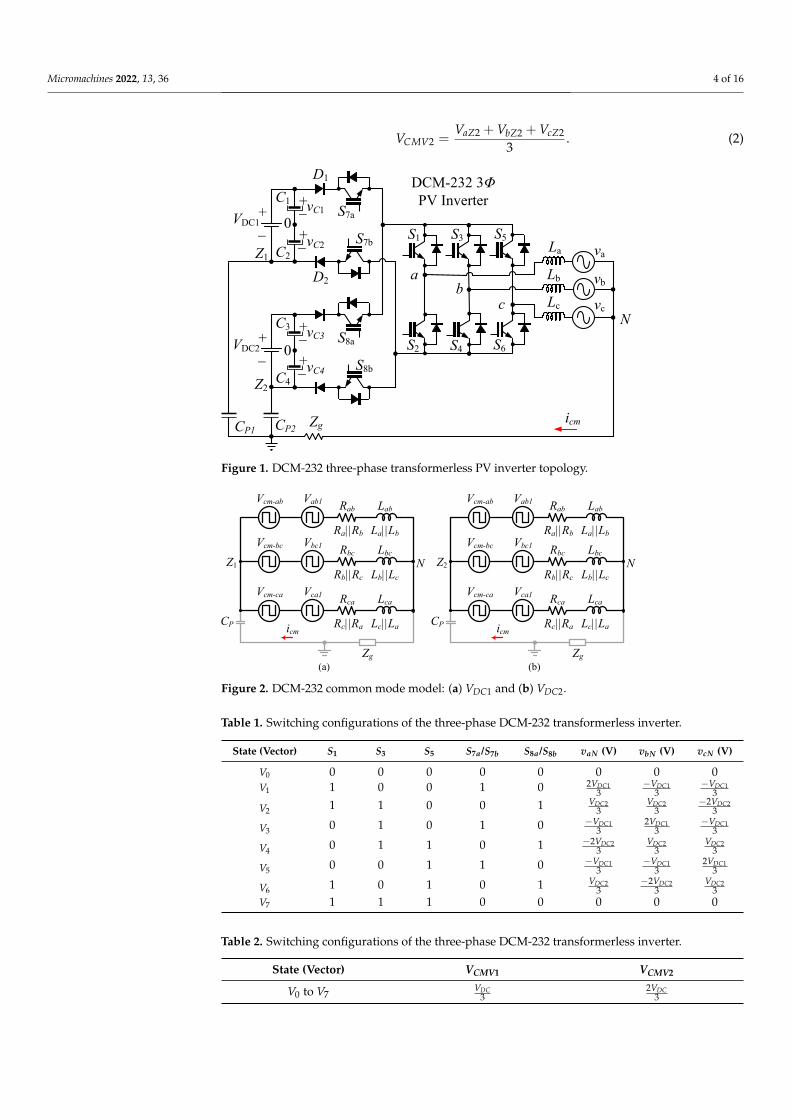
A simplified circuit of the DCM-232 topology considered for the design of the SVPWMtechniques is shown in Figure 1. One of the main considerations for the simplified circuit isthat the DC sources are assumed constant. However, in a real PV transformerless system,the voltage magnitude is slightly variable and, in that case, it is necessary to implementa solution, for example, modifying the modulation strategy or implementing a balancecontrol loop; nevertheless, this topic is out of the scope of this paper and is left for a futureresearch. Three additional important considerations of the simplified diagram are thatonly the stray capacitance generated by the PV panel are considered; the drive circuitsfor the semiconductors and control system are not included because these elements donot affect the common mode behavior. Finally, in the case of the ground impedance, thecapacitive and inductive effects are disregarded in the system. Therefore, the impedance isconsidered mainly resistive [18]. The different states that can be proposed to control theDCM-232 inverter in which the structure consists of ten switches are summarized in Table 1.As it can be observed, there are eight possible states. These states produce the followingvoltage levels between phases and the neutral connection: VDC1 = VDC2, 2VDC/3, VDC/3,0V, −VDC/3, and −2VDC/3. It is important to note that all of the states considered hereare exactly the same as in the conventional 3P-FB inverter. However, the main differenceis that the switches on the DC side, S7a,S7b, S8a, and S8b, are used to make a decouplingaction when certain active or null vectors supply the load.
2.1. DCM-232 Common Mode Model
In order to determine the CMV behavior, a CMM for the DCM-232 topology is derived.Considering the directions given in [19], the simplified CMM shown in Figure 2 can beobtained. As it can be observed, there are two separated circuits, the circuit in Figure 2acorresponds to the DC source VDC1, while the simplified circuit shown in Figure 2b corre-sponds to the DC source VDC2. Since the power sources are isolated from each other with acommon load, the obtained model is also separated and is essentially the model obtainedin [2] for the 3P-FB inverter. Based on that, the common mode voltage in this topology canbe calculated in each DC source using (1) and (2). Considering (1) and (2), the CMV can becalculated for each state defined in Table 1, and the results are shown in Table 2. It can benoted that the CMV maintains the same magnitude throughout the switching period whenthe odd vectors (V1, V3 and V5) or the even vectors (V2, V4 and V6) are connected to the loadusing VDC1 and VDC2, respectively. On the other hand, when zero vectors are generated(V0 and V7), the CMV keeps the previous value because both DC sources are decoupledfrom the load.
VCMV1 =VaZ1 + VbZ1 + VcZ1
3, (1)
Micromachines 2022, 13, 36 4 of 16
VCMV2 =VaZ2 + VbZ2 + VcZ2
3. (2)
DCM-232 3Φ
PV Inverter
S1
S2
S3
S4
S5
S6
La
Lb
Lc
va
vb
vc
N
+_
+_
+_
C1
C2
vC1
vC2
VDC1
+_
+_
+_
C3
C4
vC3
vC4
VDC2
S7a
S7b
S8a
S8b
CP2icmCP1
Zg
Z1
Z2
0
0
D1
D2a
bc
Figure 1. DCM-232 three-phase transformerless PV inverter topology.
(a)
icm
Zg
CP
Vcm-ab Vab1
Vcm-bc Vbc1
Vcm-ca Vca1
Z1 NLbc
Lb||Lc
Lca
Lc||La
Lab
La||Lb
Rab
Ra||Rb
Rbc
Rb||Rc
Rca
Rc||Ra
(b)
icm
Zg
CP
Vcm-ab Vab1
Vcm-bc Vbc1
Vcm-ca Vca1
Z2 NLbc
Lb||Lc
Lca
Lc||La
Lab
La||Lb
Rab
Ra||Rb
Rbc
Rb||Rc
Rca
Rc||Ra
Figure 2. DCM-232 common mode model: (a) VDC1 and (b) VDC2.
Table 1. Switching configurations of the three-phase DCM-232 transformerless inverter.
State (Vector) S1 S3 S5 S7a/S7b S8a/S8b vaN (V) vbN (V) vcN (V)
V0 0 0 0 0 0 0 0 0V1 1 0 0 1 0 2VDC1
3−VDC1
3−VDC1
3
V2 1 1 0 0 1 VDC23
VDC23
−2VDC23
V3 0 1 0 1 0 −VDC13
2VDC13
−VDC13
V4 0 1 1 0 1 −2VDC23
VDC23
VDC23
V5 0 0 1 1 0 −VDC13
−VDC13
2VDC13
V6 1 0 1 0 1 VDC23
−2VDC23
VDC23
V7 1 1 1 0 0 0 0 0
Table 2. Switching configurations of the three-phase DCM-232 transformerless inverter.
State (Vector) VCMV1 VCMV2
V0 to V7VDC
32VDC
3
Micromachines 2022, 13, 36 5 of 16
2.2. Proposed Space Vector PWM Techniques
The circuit theory states that a three-phase system can be represented on a α-β planeby means of the Clarke transformation, as shown in (3)–(5). Note that a simplification usingcosine functions for the three-phase voltage components (va, vb, and vc) is considered.
[vα
vβ
]=
23
[1 − 1
2 − 12
0√
32 −
√3
2
] vavbvc
, (3)
vα = Vm cos(ωt), (4)
vβ = Vm sin(ωt). (5)
Based on (4) and (5), the module and the angle of the reference vector, Vre f , can becalculated as
|Vre f | =√
vα2 + vβ
2, (6)
tan(θ) =vβ
vα. (7)
Then, substituting (4) and (5) in (7), the module of the reference vector can be redefined as
|Vre f | =√(Vm cos(ωt))2 + (Vm sin(ωt))2,
|Vre f | = Vm, (8)
and finally, from (7), the angle θ can be calculated as follows:
θ = tan−1(vβ
vα
). (9)
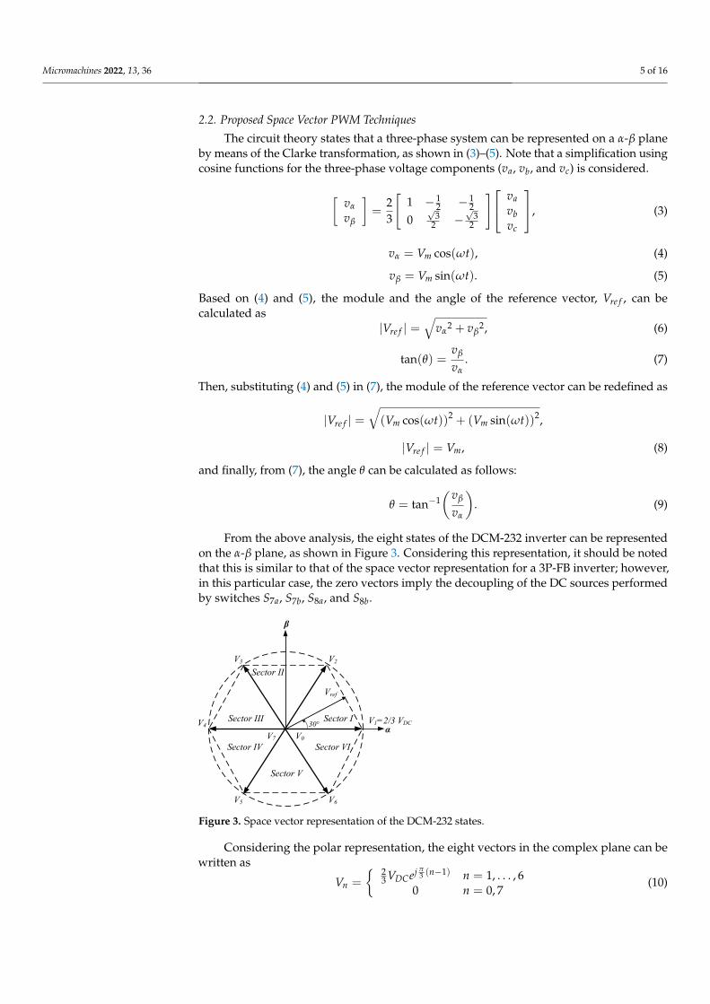
From the above analysis, the eight states of the DCM-232 inverter can be representedon the α-β plane, as shown in Figure 3. Considering this representation, it should be notedthat this is similar to that of the space vector representation for a 3P-FB inverter; however,in this particular case, the zero vectors imply the decoupling of the DC sources performedby switches S7a, S7b, S8a, and S8b.
β
α
Sector II
Sector III Sector I
Sector IV Sector VI
Sector V
V1=2/3 VDC
V2V3
V4
V5 V6
V0V7
Vref
30°
Figure 3. Space vector representation of the DCM-232 states.
Considering the polar representation, the eight vectors in the complex plane can bewritten as
Vn =
23 VDCej π
3 (n−1) n = 1, . . . , 60 n = 0, 7
(10)
Micromachines 2022, 13, 36 6 of 16
For a balanced three-phase system, Vre f can be expressed as
Vre f = Vejωt. (11)
In order to synthesize Vre f , three successive space vectors can be applied along aswitching period (Ts =
1fs
). Therefore, the addition of the applied vectors (active and/ornull) must satisfy
Vata + Vbtb + VNt0 = Vre f Ts, (12)
Notice that the switching period is the sum of the times of each applied vector:
ta + tb + t0 = Ts. (13)
To determine the duty cycles for each applied vector, the complex components (VAand VB) in the α-β plane for Vre f can be defined as
Vre f =
VA = 1
TsVata
VB = 1Ts
Vbtb.(14)
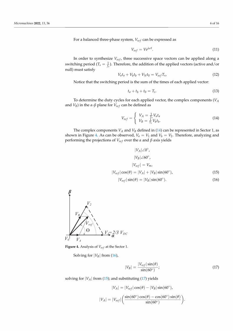
The complex components VA and VB defined in (14) can be represented in Sector 1, asshown in Figure 4. As can be observed, Va = V1 and Vb = V2. Therefore, analyzing andperforming the projections of Vre f over the α and β axis yields
|VA|∠0,
|VB|∠60,
|Vre f | = Vm,
|Vre f | cos(θ) = |VA|+ |VB| sin(60), (15)
|Vre f | sin(θ) = |VB| sin(60). (16)
V1=2/3 VDC
V2
α
β
V0
Vref
VA
VB
Ɵ
Figure 4. Analysis of Vre f at the Sector 1.
Solving for |VB| from (16),
|VB| =|Vre f | sin(θ)
sin(60); (17)
solving for |VA| from (15); and substituting (17) yields
|VA| = |Vre f | cos(θ)− |VB| sin(60),
|VA| = |Vre f |(
sin(60) cos(θ)− cos(60) sin(θ)sin(60)
).
Micromachines 2022, 13, 36 7 of 16
Then, using the following trigonometric identity,
sin(a− b) = sin(a) cos(b)− cos(a) sin(b),
yields
|VA| =|Vre f | sin(60 − θ)
sin(60). (18)
Substituting the components (14) in (17) and (18),
1Ts
Vbtb =|Vre f | sin(θ)
sin(60),
1Ts
Vata =|Vre f | sin(60 − θ)
sin(60).
Now, solving for ta,
ta =|Vre f |Ts sin(60 − θ)
Va sin(60),
and then solving for tb,
tb =|Vre f |Ts sin(θ)
Vb sin(60),
and since Va = Vb = 23 VDC and sin(60) =
√3
2 ,
ta =
√3|Vre f |Ts sin(60 − θ)
VDC(19)
and
tb =
√3|Vre f |Ts sin(θ)
VDC. (20)
Finally, solving for t0 from (13) yields
t0 = Ts − ta − tb. (21)
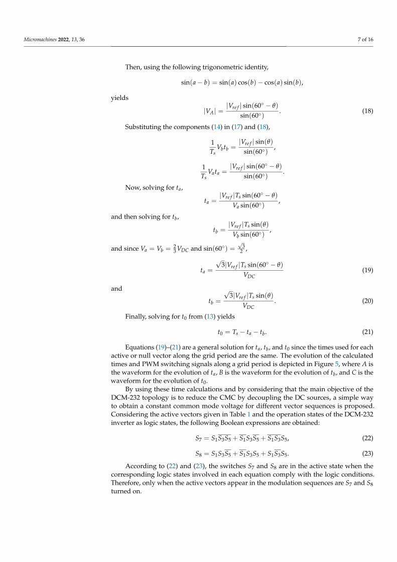
Equations (19)–(21) are a general solution for ta, tb, and t0 since the times used for eachactive or null vector along the grid period are the same. The evolution of the calculatedtimes and PWM switching signals along a grid period is depicted in Figure 5, where A isthe waveform for the evolution of ta, B is the waveform for the evolution of tb, and C is thewaveform for the evolution of t0.
By using these time calculations and by considering that the main objective of theDCM-232 topology is to reduce the CMC by decoupling the DC sources, a simple wayto obtain a constant common mode voltage for different vector sequences is proposed.Considering the active vectors given in Table 1 and the operation states of the DCM-232inverter as logic states, the following Boolean expressions are obtained:
S7 = S1S3S5 + S1S3S5 + S1S3S5, (22)
S8 = S1S3S5 + S1S3S5 + S1S3S5. (23)
According to (22) and (23), the switches S7 and S8 are in the active state when thecorresponding logic states involved in each equation comply with the logic conditions.Therefore, only when the active vectors appear in the modulation sequences are S7 and S8turned on.
Micromachines 2022, 13, 36 8 of 16
30 90 150 210 270 330 360
0.46
-0.46
0
Sectors
V VI I II III IV V
t
A B C0
1
2
3
4
5
6
t
(a)
(b)
S10
1
S3
S5
0
1
0
1
t
t
t
(c)
Figure 5. From top to bottom, (a) sectors; (b) evolution of the switching times ta, tb, and t0; and(c) switching sequences for S1, S3, and S5 in a conventional three-phase full-bridge inverter.
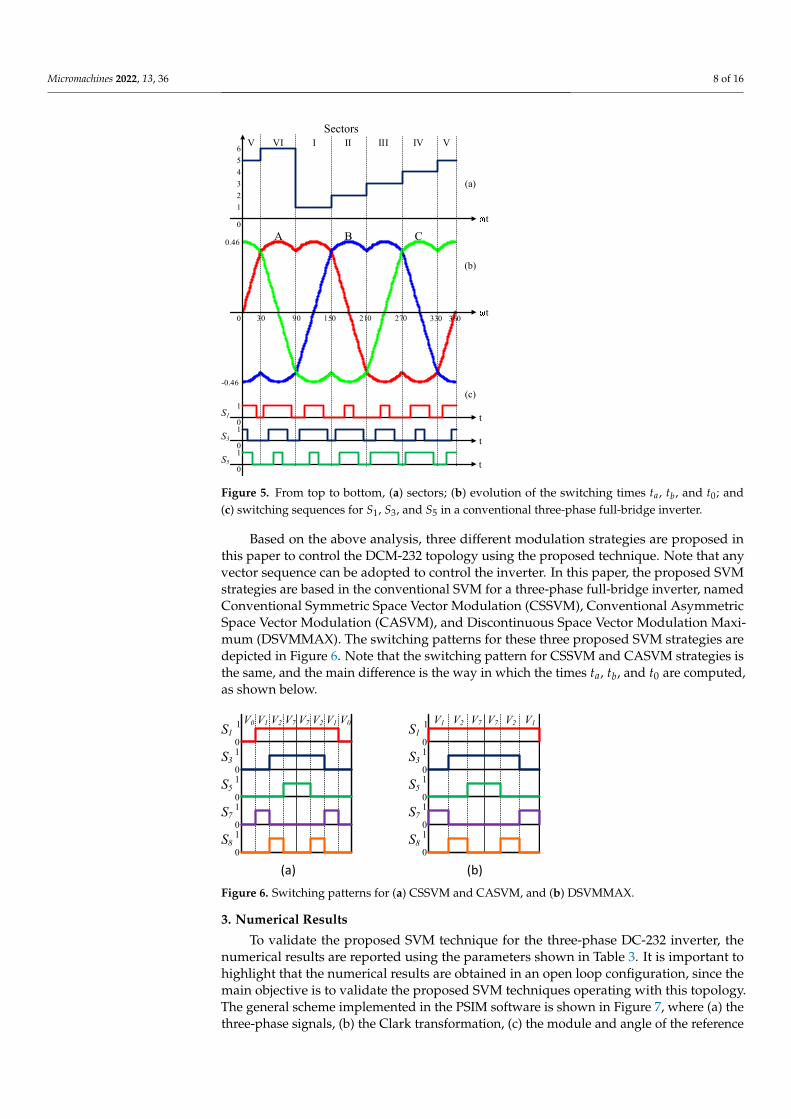
Based on the above analysis, three different modulation strategies are proposed inthis paper to control the DCM-232 topology using the proposed technique. Note that anyvector sequence can be adopted to control the inverter. In this paper, the proposed SVMstrategies are based in the conventional SVM for a three-phase full-bridge inverter, namedConventional Symmetric Space Vector Modulation (CSSVM), Conventional AsymmetricSpace Vector Modulation (CASVM), and Discontinuous Space Vector Modulation Maxi-mum (DSVMMAX). The switching patterns for these three proposed SVM strategies aredepicted in Figure 6. Note that the switching pattern for CSSVM and CASVM strategies isthe same, and the main difference is the way in which the times ta, tb, and t0 are computed,as shown below.
S10
1
S3
S5
0
1
0
1
V0 V1 V1V7 V7 V0V2 V2
S70
1
S80
1
S10
1
S3
S5
0
1
0
1
V1 V1V7 V7V2 V2
S70
1
S80
1
(a) (b)
Figure 6. Switching patterns for (a) CSSVM and CASVM, and (b) DSVMMAX.
3. Numerical Results
To validate the proposed SVM technique for the three-phase DC-232 inverter, thenumerical results are reported using the parameters shown in Table 3. It is important tohighlight that the numerical results are obtained in an open loop configuration, since themain objective is to validate the proposed SVM techniques operating with this topology.The general scheme implemented in the PSIM software is shown in Figure 7, where (a) thethree-phase signals, (b) the Clark transformation, (c) the module and angle of the reference
Micromachines 2022, 13, 36 9 of 16
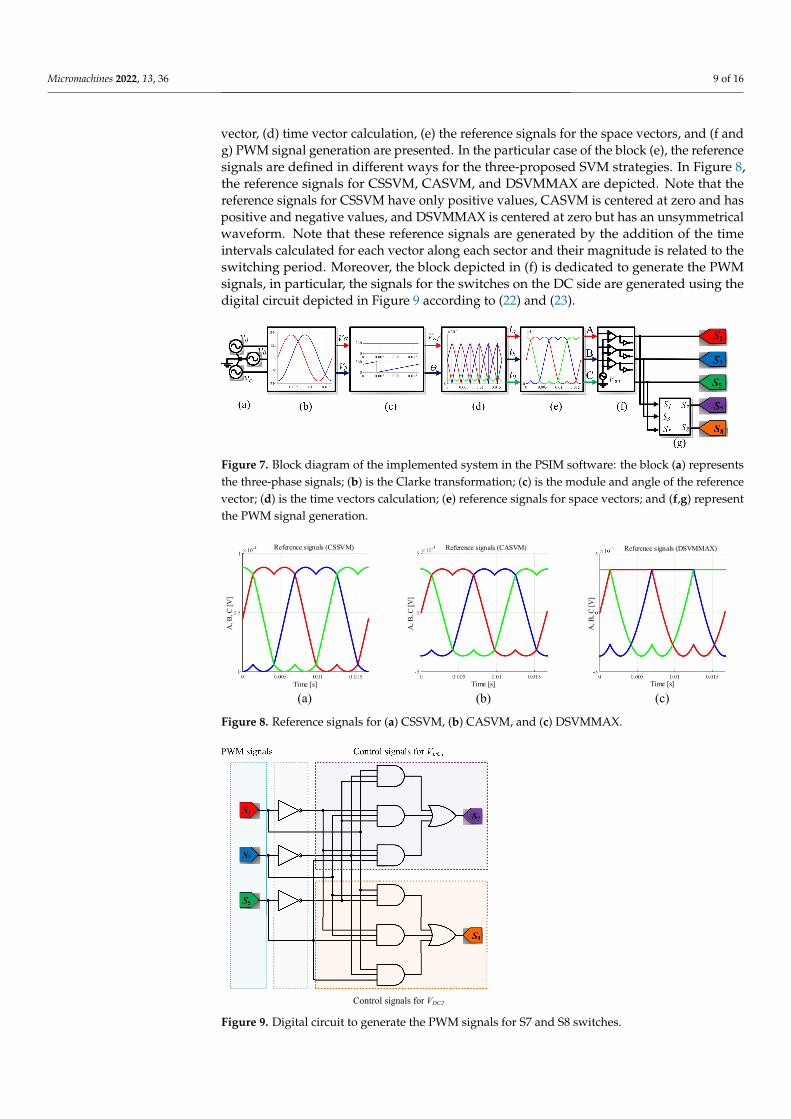
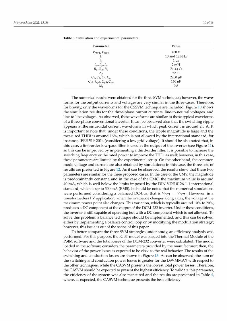
vector, (d) time vector calculation, (e) the reference signals for the space vectors, and (f andg) PWM signal generation are presented. In the particular case of the block (e), the referencesignals are defined in different ways for the three-proposed SVM strategies. In Figure 8,the reference signals for CSSVM, CASVM, and DSVMMAX are depicted. Note that thereference signals for CSSVM have only positive values, CASVM is centered at zero and haspositive and negative values, and DSVMMAX is centered at zero but has an unsymmetricalwaveform. Note that these reference signals are generated by the addition of the timeintervals calculated for each vector along each sector and their magnitude is related to theswitching period. Moreover, the block depicted in (f) is dedicated to generate the PWMsignals, in particular, the signals for the switches on the DC side are generated using thedigital circuit depicted in Figure 9 according to (22) and (23).
Figure 7. Block diagram of the implemented system in the PSIM software: the block (a) representsthe three-phase signals; (b) is the Clarke transformation; (c) is the module and angle of the referencevector; (d) is the time vectors calculation; (e) reference signals for space vectors; and (f,g) representthe PWM signal generation.
(a) (b) (c)
Reference signals (CSSVM) Reference signals (CASVM) Reference signals (DSVMMAX)
Time [s]Time [s] Time [s]
A, B
, C
[V
]
A, B
, C
[V
]
A, B
, C
[V
]
Figure 8. Reference signals for (a) CSSVM, (b) CASVM, and (c) DSVMMAX.
PW
Control signals for VDC2
Figure 9. Digital circuit to generate the PWM signals for S7 and S8 switches.
Micromachines 2022, 13, 36 10 of 16
Table 3. Simulation and experimental parameters.
Parameter Value
VDC1, VDC2 400 Vfs 10 and 12 kHztd 1 µs
La, Lb, Lc 2 mHRa, Rb, Rc 71.43 Ω
Zg 22 ΩC1, C2, C3, C4 2200 µF
Cp1, Cp2, Cp3, Cp4 160 nFMi 0.8
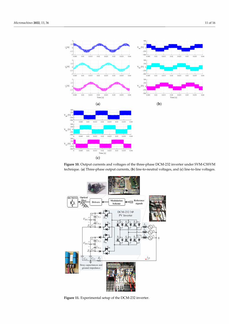
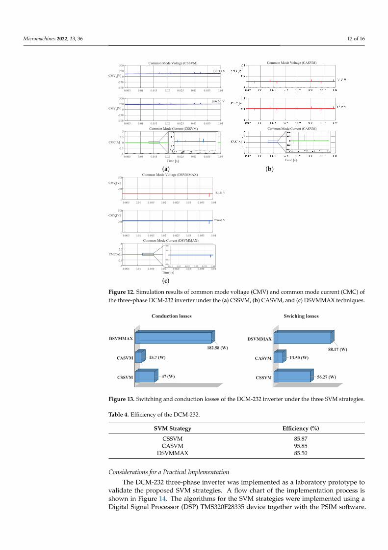
The numerical results were obtained for the three SVM techniques; however, the wave-forms for the output currents and voltages are very similar in the three cases. Therefore,for brevity, only the waveforms for the CSSVM technique are included. Figure 10 showsthe simulation results for the three-phase output currents, line-to-neutral voltages, andline-to-line voltages. As observed, these waveforms are similar to those typical waveformsof a three-phase conventional inverter. It can be observed also that the switching rippleappears at the sinusoidal current waveforms in which peak current is around 2.5 A. Itis important to note that, under these conditions, the ripple magnitude is large and themeasured THDi is around 16%, which is not allowed by the international standard, forinstance, IEEE 519-2014 (considering a low grid voltage). It should be also noted that, inthis case, a first-order low-pass filter is used at the output of the inverter (see Figure 11),so this can be improved by implementing a third-order filter. It is possible to increase theswitching frequency or the rated power to improve the THDi as well; however, in this case,these parameters are limited by the experimental setup. On the other hand, the commonmode voltage and current are also obtained by simulations; in this case, the three sets ofresults are presented in Figure 12. As it can be observed, the results show that these twoparameters are similar for the three proposed cases. In the case of the CMV, the magnitudeis predominantly constant, and in the case of the CMC, the maximum value is around40 mA, which is well below the limits imposed by the DIN VDE 0126-1-1 internationalstandard, which is up to 300 mA (RMS). It should be noted that the numerical simulationswere performed considering a balanced DC-bus, that is VDC1 = VDC2. However, in atransformerless PV application, when the irradiance changes along a day, the voltage at themaximum power point also changes. This variation, which is typically around 10% to 20%,produces a DC component at the output of the DCM-232 inverter. Under these conditions,the inverter is still capable of operating but with a DC component which is not allowed. Tosolve this problem, a balance technique should be implemented, and this can be solvedeither by implementing a balance control loop or by modifying the modulation strategy;however, this issue is out of the scope of this paper.
To better compare the three SVM strategies under study, an efficiency analysis wasperformed. For this purpose, the IGBT model was loaded into the Thermal Module of thePSIM software and the total losses of the DCM-232 converter were calculated. The modelloaded in the software considers the parameters provided by the manufacturer; then, thebehavior of the power losses is expected to be close to the real behavior. The results of theswitching and conduction losses are shown in Figure 13. As can be observed, the sum ofthe switching and conduction power losses is greater for the DSVMMAX with respect tothe other techniques, while the CASVM presents the lowest total power losses. Therefore,the CASVM should be expected to present the highest efficiency. To validate this parameter,the efficiency of the system was also measured and the results are presented in Table 4,where, as expected, the CASVM technique presents the best efficiency.
Micromachines 2022, 13, 36 11 of 16
0.005 0.01 0.015 0.02 0.025 0.03 0.035 0.04-5
-2.5
0
2.5
5
0.005 0.01 0.015 0.02 0.025 0.03 0.035 0.04-5
-2.5
0
2.5
5
0.02
Time [s]
0.005 0.01 0.015 0.025 0.03 0.035 0.04-5
-2.5
0
2.5
5
ia[A]
ic[A]
ib[A]
0.005 0.01 0.015 0.02 0.025 0.03 0.035 0.04-500
-250
0
250
500
0.005 0.01 0.015 0.02 0.025 0.03 0.035 0.04-500
-250
0
250
500
0.02
Time [s]
0.005 0.01 0.015 0.025 0.03 0.035 0.04-500
-250
0
250
500
Vbn[V]
Vcn[V]
Van[V]
(a) (b)
0 0.005 0.01 0.015 0.02 0.025 0.03 0.035 0.04-500
-250
0
250
500
0 0.005 0.01 0.015 0.02 0.025 0.03 0.035 0.04-500
-250
0
250
500
0.02
Time [s]
0 0.005 0.01 0.015 0.025 0.03 0.035 0.04-500
-250
0
250
500
Vab[V]
Vbc[V]
Vca[V]
(c)
Figure 10. Output currents and voltages of the three-phase DCM-232 inverter under SVM-CSSVMtechnique. (a) Three-phase output currents, (b) line-to-neutral voltages, and (c) line-to-line voltages.
DCM-232 3Φ
PV Inverter
S1
S2
S3
S4
S5
S6
La
Lb
Lc
va
vb
vc
N
+_
+_
+_
C1
C2
vC1
vC2
VDC1
+_
+_
+_
C3
C4
vC3
vC4
VDC2
S7a
S7b
S8a
S8b
CP2icmCP1
Zg
Z1
Z2
0
0
Stray capacitances and
ground impedance
CPLD Cool
Runner II DSP
F28335
Modulation
Scheme
Optical
fiber Reference
signals
DCM332
Drivers
DCM-232 3Φ
PV Inverter
Output filter
Figure 11. Experimental setup of the DCM-232 inverter.
Micromachines 2022, 13, 36 12 of 16
0.005 0.01 0.015 0.02 0.025 0.03 0.035 0.04-500
-250
0
250
500Voltaje de modo común (CMV)
0.005 0.01 0.015 0.02 0.025 0.03 0.035 0.04-500
-250
0
250
500
Tiempo [s]
0.005 0.01 0.015 0.02 0.025 0.03 0.035 0.04-5
-2.5
0
2.5
5Corriente de modo común (CMC)
CMV1[V]
CMV2[V]
CMC[A]
Common Mode Voltage (CSSVM)
Common Mode Current (CSSVM)
Time [s]
133.33 V
266.66 V
Common Mode Voltage (CASVM)
Common Mode Current (CASVM)
Time [s]
(a) (b)
0.005 0.01 0.015 0.02 0.025 0.03 0.035 0.040
250
500Voltaje de modo común (CMV)
0.005 0.01 0.015 0.02 0.025 0.03 0.035 0.040
250
500
Tiempo [s
0.005 0.01 0.015 0.02 0.025 0.03 0.035 0.04-5
-2.5
0
2.5
5Corriente de modo común (CMC)
CMV1[V]
CMV2[V]
CMC[A]
133.33 V
266.66 V
Common Mode Voltage (DSVMMAX)
Common Mode Current (DSVMMAX)
Time [s]
(c)
Figure 12. Simulation results of common mode voltage (CMV) and common mode current (CMC) ofthe three-phase DCM-232 inverter under the (a) CSSVM, (b) CASVM, and (c) DSVMMAX techniques.
CS VM
C
D
47 (W)
15.7 (W)
182.58 (W)
CS VM
C
D
56.27 (W)
13.50 (W)
88.17 (W)
Figure 13. Switching and conduction losses of the DCM-232 inverter under the three SVM strategies.
Table 4. Efficiency of the DCM-232.
SVM Strategy Efficiency (%)
CSSVM 85.87CASVM 95.85
DSVMMAX 85.50
Considerations for a Practical Implementation
The DCM-232 three-phase inverter was implemented as a laboratory prototype tovalidate the proposed SVM strategies. A flow chart of the implementation process isshown in Figure 14. The algorithms for the SVM strategies were implemented using aDigital Signal Processor (DSP) TMS320F28335 device together with the PSIM software.
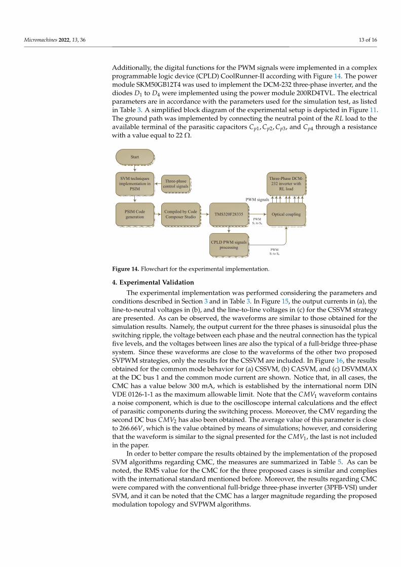
Micromachines 2022, 13, 36 13 of 16
Additionally, the digital functions for the PWM signals were implemented in a complexprogrammable logic device (CPLD) CoolRunner-II according with Figure 14. The powermodule SKM50GB12T4 was used to implement the DCM-232 three-phase inverter, and thediodes D1 to D4 were implemented using the power module 200RD4TVL. The electricalparameters are in accordance with the parameters used for the simulation test, as listedin Table 3. A simplified block diagram of the experimental setup is depicted in Figure 11.The ground path was implemented by connecting the neutral point of the RL load to theavailable terminal of the parasitic capacitors Cp1, Cp2, Cp3, and Cp4 through a resistancewith a value equal to 22 Ω.
Figure 14. Flowchart for the experimental implementation.
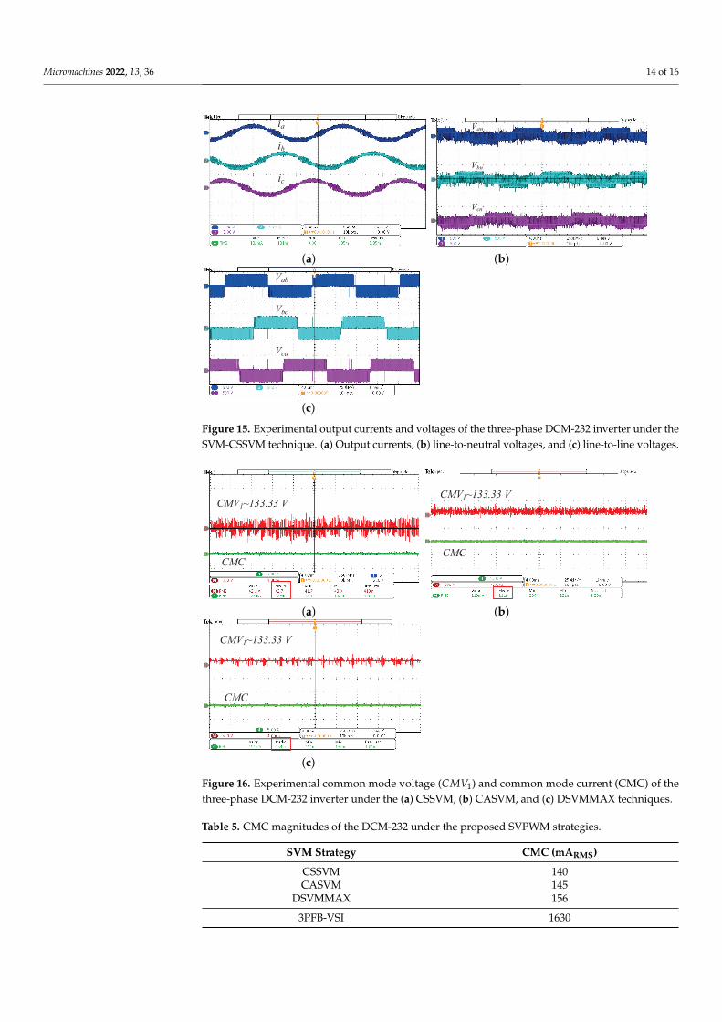
4. Experimental Validation
The experimental implementation was performed considering the parameters andconditions described in Section 3 and in Table 3. In Figure 15, the output currents in (a), theline-to-neutral voltages in (b), and the line-to-line voltages in (c) for the CSSVM strategyare presented. As can be observed, the waveforms are similar to those obtained for thesimulation results. Namely, the output current for the three phases is sinusoidal plus theswitching ripple, the voltage between each phase and the neutral connection has the typicalfive levels, and the voltages between lines are also the typical of a full-bridge three-phasesystem. Since these waveforms are close to the waveforms of the other two proposedSVPWM strategies, only the results for the CSSVM are included. In Figure 16, the resultsobtained for the common mode behavior for (a) CSSVM, (b) CASVM, and (c) DSVMMAXat the DC bus 1 and the common mode current are shown. Notice that, in all cases, theCMC has a value below 300 mA, which is established by the international norm DINVDE 0126-1-1 as the maximum allowable limit. Note that the CMV1 waveform containsa noise component, which is due to the oscilloscope internal calculations and the effectof parasitic components during the switching process. Moreover, the CMV regarding thesecond DC bus CMV2 has also been obtained. The average value of this parameter is closeto 266.66V, which is the value obtained by means of simulations; however, and consideringthat the waveform is similar to the signal presented for the CMV1, the last is not includedin the paper.
In order to better compare the results obtained by the implementation of the proposedSVM algorithms regarding CMC, the measures are summarized in Table 5. As can benoted, the RMS value for the CMC for the three proposed cases is similar and complieswith the international standard mentioned before. Moreover, the results regarding CMCwere compared with the conventional full-bridge three-phase inverter (3PFB-VSI) underSVM, and it can be noted that the CMC has a larger magnitude regarding the proposedmodulation topology and SVPWM algorithms.
Micromachines 2022, 13, 36 14 of 16
ia
ib
ic
Van
Vbn
Vcn
(a) (b)Vab
Vbc
Vca
(c)
Figure 15. Experimental output currents and voltages of the three-phase DCM-232 inverter under theSVM-CSSVM technique. (a) Output currents, (b) line-to-neutral voltages, and (c) line-to-line voltages.
CMV1~133.33 V
CMC
CMV1~133.33 V
CMC
(a) (b)
CMV1~133.33 V
CMC
(c)
Figure 16. Experimental common mode voltage (CMV1) and common mode current (CMC) of thethree-phase DCM-232 inverter under the (a) CSSVM, (b) CASVM, and (c) DSVMMAX techniques.
Table 5. CMC magnitudes of the DCM-232 under the proposed SVPWM strategies.
SVM Strategy CMC (mARMS)
CSSVM 140CASVM 145
DSVMMAX 156
3PFB-VSI 1630

Micromachines 2022, 13, 36 15 of 16
5. Conclusions
In this paper, three hybrid modulation strategies were proposed. The proposed modu-lation strategies combine the time calculations of the space vector modulation techniqueand the comparison of the reference signals with a carrier triangular waveform, as does thesinusoidal pulse width modulation strategies. The results show that the SVM algorithmsfor the DCM-232 can be implemented using this combined method, which is convenientfor practical implementation in a digital platform. Moreover, an evaluation of the efficiencywas performed, and the results show that the modulation sequence has an importanteffect on this parameter. This analysis demonstrates that the CASVM technique has thehighest efficiency (95.85%) among the proposed modulations algorithms, although all ofthe proposed methods present an efficiency above 85.5%. Finally, it can be also concludedthat any of the proposed techniques is capable of reducing the magnitude of the commonmode current (i.e., up to 140 mARMS for the CSSVM technique), which is a very interestingfeature for transformerless photovoltaic applications since the power inverter operationcomplies with the international standards.
Author Contributions: All authors contributed to the development of the overall document, spacevector modulation design, analysis, simulations, and experimental results. All authors have read andagreed to the published version of the manuscript.
Funding: This research was partially funded by Tecnologico Nacional de Mexico under the project10138.21-PD.
Conflicts of Interest: The authors declare no conflict of interest.
AbbreviationsThe following abbreviations are used in this paper:
PWM Pulse Width ModulationDC Direct CurrentDC-AC Direct Current–Alternating CurrentPV PhotovoltaicLKC Leakage Currents3P-CMI Three-Phase Cascade Multilevel InverterCMV Common-Mode VoltageCMC Common-Mode CurrentTHD Total Harmonic DistortionRMS Root Mean SquareNPC Neutral Point Clampled3P-FB Six-Switch Three-Phase InverterNSPWM Near-State Pulse Width Modulation3P-FBSC Six-Switch Three-Phase Inverter with Split Capacitor3P-NPC Three-Phase Neutral Point Clamped InverterSVM Space Vector ModulationIGBT Isolated Gate Bipolar TransistorMOSFET Metal-Oxide Semiconductor Field-Effect TransistorHERIC Highly Efficient and Reliable Inverter ConceptSVPWM Space Vector Pulse Width ModulationCPLD Complex Programmable Logic DeviceCMM Common-Mode ModelCSSVM Conventional Symmetric Space Vector ModulationCASVM Conventional Asymmetric Space Vector ModulationDSVMMAX Discontinuous Space Vector Modulation MaximumDSP Digital Signal Processor

Micromachines 2022, 13, 36 16 of 16
References1. Un, E.; Hava, A.M. A Near-State PWM Method With Reduced Switching Losses and Reduced Common-Mode Voltage for
Three-Phase Voltage Source Inverters. IEEE Trans. Ind. Appl. 2009, 45, 782–793. [CrossRef]2. Kerekes, T.; Teodorescu, R.; Liserre, M.; Klumpner, C.; Sumner, M. Evaluation of Three-Phase Transformerless Photovoltaic
Inverter Topologies. IEEE Trans. Power Electron. 2009, 24, 2202–2211. [CrossRef]3. Huang, Y.; Shen, M.; Peng, F.Z.; Wang, J. Z-Source Inverter for Residential Photovoltaic Systems. IEEE Trans. Power Electron. 2006,
21, 1776–1782. [CrossRef]4. Bradaschia, F.; Cavalcanti, M.C.; Ferraz, P.E.P.; Neves, F.A.S.; dos Santos, E.C.; da Silva, J.H.G.M. Modulation for Three-Phase
Transformerless Z-Source Inverter to Reduce Leakage Currents in Photovoltaic Systems. IEEE Trans. Ind. Electron. 2011, 58,5385–5395. [CrossRef]
5. Park, J.; Kim, H.; Nho, E.; Chun, T.; Choi, J. Grid-connected PV System Using a Quasi-Z-source Inverter. In Proceedings of the 2009Twenty-Fourth Annual IEEE Applied Power Electronics Conference and Exposition, Washington, DC, USA, 15–19 February 2009;pp. 925–929.
6. Li, Y.; Anderson, J.; Peng, F.Z.; Liu, D. Quasi-Z-Source Inverter for Photovoltaic Power Generation Systems. In Proceed-ings of the 2009 Twenty-Fourth Annual IEEE Applied Power Electronics Conference and Exposition, Washington, DC, USA,15–19 February 2009; pp. 918–924.
7. Anderson, J.; Peng, F.Z. Four quasi-Z-Source inverters. In Proceedings of the 2008 IEEE Power Electronics Specialists Conference,Rhodes, Greece, 15–19 June 2008; pp. 2743–2749.
8. Vazquez, G.; Kerekes, T.; Rocabert, J.; Rodriguez, P.; Teodorescu, R.; Aguilar, D. A photovoltaic three-phase topology to reduceCommon Mode Voltage. In Proceedings of the 2010 IEEE International Symposium on Industrial Electronics, Bari, Italy,4–7 July 2010; pp. 2885–2890.
9. Li, W.; Gu, Y.; Luo, H.; Cui, W.; He, X.; Xia, C. Topology Review and Derivation Methodology of Single-Phase TransformerlessPhotovoltaic Inverters for Leakage Current Suppression. IEEE Trans. Ind. Electron. 2015, 62, 4537–4551. [CrossRef]
10. Xiao, H.; Xie, S.; Chen, Y.; Huang, R. An optimized transformerless photovoltaic grid-connected inverter. IEEE Trans. Ind. Electron.2011, 58, 1887–1895. [CrossRef]
11. Kheng Suan, F.T.; Rahim, N.A.; Ping, H.W. Three-phase transformerless grid-connected photovoltaic inverter to reduceleakage currents. In Proceedings of the IEEE Conference on Clean Energy and Technology (CEAT), Lankgkawi, Malaysia,18–20 November 2013; pp. 277–280.
12. Freddy, T.K.S.; Rahim, N.A.; Hew, W.; Che, H.S. Modulation Techniques to Reduce Leakage Current in Three-Phase Transformer-less H7 Photovoltaic Inverter. IEEE Trans. Ind. Electron. 2015, 62, 322–331. [CrossRef]
13. Rahimi, R.; Farhangi, S.; Farhangi, B.; Moradi, G.R.; Afshari, E.; Blaabjerg, F. H8 Inverter to Reduce Leakage Current inTransformerless Three-Phase Grid-Connected Photovoltaic systems. IEEE J. Emerg. Sel. Top. Power Electron. 2018, 6, 910–918.[CrossRef]
14. Zhou, L.; Gao, F.; Shen, G.; Xu, T.; Wang, W. Low leakage current transformerless three-phase photovoltaic inverter. In Proceedingsof the 2016 IEEE Energy Conversion Congress and Exposition (ECCE), Milwaukee, WI, USA, 18–22 September 2016; pp. 1–5.
15. Kerekes, T.; Teodorescu, R.; Rodriguez, P.; Vazquez, G.; Aldabas, E. A New High-Efficiency Single-Phase Transformerless PVInverter Topology. IEEE Trans. Ind. Appl. 2011, 58, 184–191. [CrossRef]
16. Rodriguez, P.; Munoz-Aguilar, R.S.; Vazquez, G.; Candela, I.; Aldabas, E.; Etxeberria-Otadui, I. DCM-232 converter: A PVtransformerless three-phase inverter. In Proceedings of the IECON 2011-37th Annual Conference of the IEEE IndustrialElectronics Society, Melbourne, Australia, 7–10 November 2011; pp. 3876–3881.
17. Guo, X.; Xu, D.; Wu, B. New control strategy for DCM-232 three-phase PV inverter with constant common mode voltage andanti-islanding capability. In Proceedings of the 2014 IEEE Energy Conversion Congress and Exposition (ECCE), Pittsburgh, PA,USA, 14–18 September 2014; pp. 5613–5617.
18. Noroozi, N.; Zolghadri, M.R.; Yaghoubi, M. A novel modulation method for reducing common mode voltage in three-phaseinverters. In Proceedings of the Environment and Electrical Engineering and 2017 IEEE Industrial and Commercial PowerSystems Europe (EEEIC/I&CPS Europe), Italy, Milan, 6–9 June 2017; pp. 1–5.
19. Gubia, E.; Sanchis, P.; Ursua, A.; Lopez, J.; Marroyo, L. Ground currents in single-phase transformerless photovoltaic systems.Prog. Photovolt. Res. Appl. 2007, 15, 629–650. [CrossRef]