Hybrid Clock Recovery for a Gigabit POF Transceiver Implemented on FPGA
6
2988 JOURNAL OF LIGHTWAVE TECHNOLOGY, VOL. 31, NO. 18, SEPTEMBER 15, 2013 Hybrid Clock Recovery for a Gigabit POF Transceiver Implemented on FPGA Julio Ram´ ırez, Antonino Nespola, Stefano Straullu, Paolo Savio, Silvio Abrate, Member, IEEE, and Roberto Gaudino, Senior Member, IEEE Abstract—In this paper, we present a clock recovery system im- plemented on field programmable gate array and integrated to the Gigabit Ethernet media converter for PMMA SI-POF developed within the framework of the POF-PLUS EU Project. We demon- strate timing synchronizing using only one sample per symbol from a highly distorted and attenuated 2-PAM signal without requiring any sort of preequalization. This is achieved by means of a hybrid analog–digital PLL with a timing error detector based on a modi- fied version of the M ¨ uller and Mueller algorithm, a loop filter, and a VCXO. Index Terms—Clock recovery (CR), DSP, field programmable gate array (FPGA), gigabit ethernet, optical communications, phase-locked loop (PLL), polymer optical fiber, timing error de- tector (TED). I. INTRODUCTION I N recent years, the increasing demand for bandwidth has driven the demand for higher performance. As a conse- quence, traditional communication solutions have been dra- matically improved and significant research efforts have led to the creation of new technologies capable to cope with ever- increasing requirements. As a part of this trend, European Tele- com Operators, together with the European Union, have been actively working and creating policies to bring broadband access to the European continent. In this sense, the European Seventh Framework Program 7 (FP7) hosted the POF-PLUS Project [1], an initiative aimed to promote research and development of short-range optical communication solutions based on plastic optical fiber (POF) to provide wired and wireless services for in-building/in-home networks and to investigate the feasibility of optical interconnects applications. As reported in [2] and [3], this initiative led to the implementation on a field programmable gate array (FPGA) of a Gigabit Ethernet media converter in full compliance with the IEEE 802.3 Ethernet Standard and capable of overcoming the impairments introduced by the POF channel. As shown in [4], the most critical issue in POF transmission schemes is to overcome the severe limitations in terms of avail- able channel bandwidth. In fact, the electrical to electrical available 6-dB bandwidth (from the electrical input of the transmitter to the electrical Manuscript received February 13, 2013; revised July 12, 2013; accepted July 30, 2013. Date of publication August 6, 2013; date of current version August 29, 2013. The authors are with PhotonLab, Istituto Superiore Mario Boella, 10138 Torino, Italy (e-mail: [email protected]; [email protected]; [email protected]; [email protected]; [email protected]; [email protected]). Digital Object Identifier 10.1109/JLT.2013.2276767 output of the photodiode) is below 100 MHz, while the media converter transmits above 1 Gbit/s. As a result, the received eye diagram is completely closed due to intersymbol interference. On top of this, due to fiber attenuation, the received signal after the POF target length is very small, so the signal to noise ratio is also very small. The key elements of the proposed architecture are thus as follows. A highly optimized equalization algorithm to overcome intersymbol interference (explained in detail in [2]). Forward error correction (FEC) in the form of a (255, 237) Reed–Solomon (RS) code [2]. A clock recovery system based on a properly optimized phase-locked loop (PLL), thereby able to recover synchro- nism with a completely closed eye diagram. As stated in [3], the first versions of the transceiver did not include a clock recovery (CR) system, therefore, in order to test and debug the proposed architecture, it was necessary to bypass the clock between the transmitting and receiving nodes. In summary, the system was able to perform 2-pulse amplitude modulation (PAM), reso- nant cavity light emitting diode (RC-LED)-based trans- mission over 50+ m of standard A4a.2 1 mm poly-methyl- methacrylate step-index plastic optical fiber (PMMA SI-POF) with a high optical power margin of 4 dB; to run real traffic, implementing a complete media con- verter between standard Gigabit Ethernet 1000Base-T and the PMMA SI-POF. After having successfully validated the operation of this first prototype, we proceeded to complete it by implementing the required timing recovery system. In this paper, we describe the chosen CR architecture and its hardware implementation on FPGA. In particular, we demonstrate the timing recovery capabilities of the system for continuous-mode data transmission based on 2-PAM signals without requiring preequalizing schemes and achieving the full functionality of the previously validated media converter. Next section will present the designing process of the system. II. TIMING RECOVERY SYSTEM A. POF Channel The first step of the design process consists of obtaining an expression to model the impairments inflicted by the POF channel on the received signal. Accordingly, the analysis starts by proposing the block dia- gram shown in Fig. 1, from which the overall transfer function 0733-8724 © 2013 IEEE
-
Upload
independent -
Category
Documents
-
view
4 -
download
0
Transcript of Hybrid Clock Recovery for a Gigabit POF Transceiver Implemented on FPGA

2988 JOURNAL OF LIGHTWAVE TECHNOLOGY, VOL. 31, NO. 18, SEPTEMBER 15, 2013
Hybrid Clock Recovery for a Gigabit POFTransceiver Implemented on FPGA
Julio Ramırez, Antonino Nespola, Stefano Straullu, Paolo Savio, Silvio Abrate, Member, IEEE,and Roberto Gaudino, Senior Member, IEEE
Abstract—In this paper, we present a clock recovery system im-plemented on field programmable gate array and integrated to theGigabit Ethernet media converter for PMMA SI-POF developedwithin the framework of the POF-PLUS EU Project. We demon-strate timing synchronizing using only one sample per symbol froma highly distorted and attenuated 2-PAM signal without requiringany sort of preequalization. This is achieved by means of a hybridanalog–digital PLL with a timing error detector based on a modi-fied version of the Muller and Mueller algorithm, a loop filter, anda VCXO.
Index Terms—Clock recovery (CR), DSP, field programmablegate array (FPGA), gigabit ethernet, optical communications,phase-locked loop (PLL), polymer optical fiber, timing error de-tector (TED).
I. INTRODUCTION
IN recent years, the increasing demand for bandwidth hasdriven the demand for higher performance. As a conse-
quence, traditional communication solutions have been dra-matically improved and significant research efforts have ledto the creation of new technologies capable to cope with ever-increasing requirements. As a part of this trend, European Tele-com Operators, together with the European Union, have beenactively working and creating policies to bring broadband accessto the European continent. In this sense, the European SeventhFramework Program 7 (FP7) hosted the POF-PLUS Project [1],an initiative aimed to promote research and development ofshort-range optical communication solutions based on plasticoptical fiber (POF) to provide wired and wireless services forin-building/in-home networks and to investigate the feasibilityof optical interconnects applications. As reported in [2] and [3],this initiative led to the implementation on a field programmablegate array (FPGA) of a Gigabit Ethernet media converter in fullcompliance with the IEEE 802.3 Ethernet Standard and capableof overcoming the impairments introduced by the POF channel.As shown in [4], the most critical issue in POF transmissionschemes is to overcome the severe limitations in terms of avail-able channel bandwidth.
In fact, the electrical to electrical available 6-dB bandwidth(from the electrical input of the transmitter to the electrical
Manuscript received February 13, 2013; revised July 12, 2013; accepted July30, 2013. Date of publication August 6, 2013; date of current version August29, 2013.
The authors are with PhotonLab, Istituto Superiore Mario Boella,10138 Torino, Italy (e-mail: [email protected]; [email protected];[email protected]; [email protected]; [email protected]; [email protected]).
Digital Object Identifier 10.1109/JLT.2013.2276767
output of the photodiode) is below 100 MHz, while the mediaconverter transmits above 1 Gbit/s. As a result, the received eyediagram is completely closed due to intersymbol interference.On top of this, due to fiber attenuation, the received signal afterthe POF target length is very small, so the signal to noise ratio isalso very small. The key elements of the proposed architectureare thus as follows.
� A highly optimized equalization algorithm to overcomeintersymbol interference (explained in detail in [2]).
� Forward error correction (FEC) in the form of a (255, 237)Reed–Solomon (RS) code [2].
� A clock recovery system based on a properly optimizedphase-locked loop (PLL), thereby able to recover synchro-nism with a completely closed eye diagram.
As stated in [3], the first versions of the transceiver did notinclude a clock recovery (CR) system, therefore, in order totest and debug the proposed architecture, it was necessary tobypass the clock between the transmitting and receiving nodes.In summary, the system was able
� to perform 2-pulse amplitude modulation (PAM), reso-nant cavity light emitting diode (RC-LED)-based trans-mission over 50+ m of standard A4a.2 1 mm poly-methyl-methacrylate step-index plastic optical fiber (PMMASI-POF) with a high optical power margin of 4 dB;
� to run real traffic, implementing a complete media con-verter between standard Gigabit Ethernet 1000Base-T andthe PMMA SI-POF.
After having successfully validated the operation of this firstprototype, we proceeded to complete it by implementing therequired timing recovery system.
In this paper, we describe the chosen CR architectureand its hardware implementation on FPGA. In particular, wedemonstrate the timing recovery capabilities of the system forcontinuous-mode data transmission based on 2-PAM signalswithout requiring preequalizing schemes and achieving the fullfunctionality of the previously validated media converter. Nextsection will present the designing process of the system.
II. TIMING RECOVERY SYSTEM
A. POF Channel
The first step of the design process consists of obtainingan expression to model the impairments inflicted by the POFchannel on the received signal.
Accordingly, the analysis starts by proposing the block dia-gram shown in Fig. 1, from which the overall transfer function
0733-8724 © 2013 IEEE

RAMIREZ et al.: HYBRID CLOCK RECOVERY FOR A GIGABIT POF TRANSCEIVER IMPLEMENTED ON FPGA 2989
Fig. 1. Block diagram of the POF channel.
for the POF channel can be derived as
P (ω) = HTX(ω) · HPOF(ω) · HRX(ω). (1)
where HP OF (ω) is modeled as a linear time invariant (LTI)low-pass filter, while HT X (ω) and HRX (ω) correspond to thetheoretical transfer functions of the 2-PAM transmitter plus RC-LED and the optoelectronic receiver PD, respectively. Once thechannel is modeled, the signal at the output of the optoelectronicreceiver YR (t) can be expressed as
YR (t) =n=∞∑
n=−∞xnp(t − εT ) + v(t) (2)
where xn denotes the transmitted 2-PAM symbols, v(t) is the in-herent additive colored Gaussian noise introduced during the op-toelectronic conversion, and εT is the unknown fractional timedelay between transmitter and the receiver (−1/2 < ε <1/2).
In order to maximize noise immunity, YR (t) must be sampledat instants of maximum eye opening, referred as optimum sam-pling instants; their individuation implies adjusting the phaseof the sampling clock according to εT . For this purpose, thereceiver must contain a clock synchronizer, which is a devicethat makes the estimation ε of the mentioned delay [5].
There are two main types of clock synchronizers, which arecategorized, depending on their architecture schemes, as feedforward and feedback synchronizers, the latter also referred aserror-tracking synchronizers [5]. Further classifications basedon other criteria can be made. For instance, if the synchronizerrelies on decided symbols to produce a timing estimate, thenit is defined as decision directed, otherwise, it is nondata aided[5]. Moreover, it can be further categorized depending on itsoperation domain, i.e., analog or digital, as being a continuousor discrete time system; and depending on the data transmissionmode as being a burst or continuous mode clock synchronizer.
For the present case, it was decided to implement acontinuous-mode and nondata-aided error-tracking synchro-nizer by means of a hybrid analog–digital architecture.
B. Hybrid Synchronizer Architecture
The general diagram of the resulting system is depicted inFig. 2. As seen, the incoming symbols transmitted at a linerate of 1.0991 Gbps (nominally 1.1 Gbps) are sampled by theon board analog to digital converter (ADC), which operates indouble data rate (DDR) mode, then the samples are forwardedto the timing error detector (TED), based on the Muller andMueller (M&M) algorithm [6], then the error signal is averagedby the loop filter, and finally, is converted to the analog domainby a Δ-Σ modulator followed by an RC filter, which togetheroperate as DAC [7] and drive the VCO. It is, hence, evident that
Fig. 2. Hybrid clock recovery architecture.
Fig. 3. M&M typical implementation.
error-tracking synchronizers apply the PLL concept to derive asampling clock from the received signal [5].
Furthermore, it should be noticed that in order to maximizeflexibility and ease eventual upgrades, it was decided to imple-ment most of the system inside the FPGA, so that the scalabilityof our architecture toward higher bit rates is mostly limited bythe analog devices present in the loop, and in particular, bythe capabilities of the ADC converter. Due to the architectureshown in Fig. 2, this is the “fastest” and the most critical circuitrequired since, inside the FPGA, all the subsequent signal pro-cessing is done using highly parallelized algorithms. In fact, theused FPGA clock is 275 MHz, significantly smaller than the bitrate.
In the following, the design and implementation of each blockcomposing this hybrid architecture is presented.
C. Muller and Mueller TED
As aforementioned, the M&M TED is implemented accord-ing to the timing recovering methods proposed in [6]. Typicallydefined as a decision-directed synchronizer [5], its conventionalimplementation diagram, as part of a clock recovery system, isshown in Fig. 3.
As seen, this device derives the delay εT by estimating theerror ek between the equalized PAM signal YS (k) and the de-cided symbols ak so that assuming sample times t = kT, wehave that the error for the kth symbol is expressed as [6]
ek = ak−1YS (kT + εT ) − akYS ((k − 1)T + εT ). (3)
As it can be noticed, the diagram shown in Fig. 3 differs fromthe architecture proposed in Fig. 2 in the way in which ek isderived so that instead of estimating the phase error based on
2990 JOURNAL OF LIGHTWAVE TECHNOLOGY, VOL. 31, NO. 18, SEPTEMBER 15, 2013
Fig. 4. S-curve of the M&M TED.
the preequalized signal YS (k) and its corresponding decidedsymbol, the M&M TED is modified in such a way that it requiresonly the unequalized received samples YR (k). The redefinedM&M algorithm can be expressed as
ek = signk−1YR (kT + εT ) − signkYR ((k − 1)T + εT ) (4)
where signk denotes the sign of the kth sample of the receivedsignal YR (k).
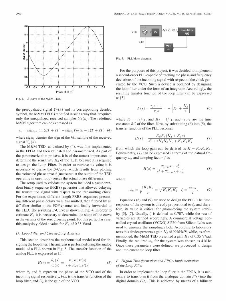
The M&M TED, as defined by (4), was first implementedin the FPGA and then validated and parameterized. As part ofthe parameterization process, it is of the utmost importance todetermine the sensitivity Kd of the TED, because it is requiredto design the Loop Filter. In order to retrieve its value it isnecessary to derive the S-Curve, which results from plottingthe estimated phase error ε (measured at the output of the TEDoperating in open loop) versus the actual phase difference.
The setup used to validate the system included a pseudoran-dom binary sequence (PRBS) generator that allowed delayingthe transmitted signal with respect to the transmitting clock.For the experiment, different length PRBS sequences present-ing different phase delays were transmitted, then filtered by anRC filter similar to the POF channel and finally forwarded tothe TED. The resulting S-Curve is shown in Fig. 4. In order toestimate Kd it is necessary to determine the slope of the curvein the vicinity of the zero crossing point. For this particular case,this analysis yielded a value for Kd of 0.35 V/rad.
D. Loop Filter and Closed-Loop Analysis
This section describes the mathematical model used for de-signing the loop filter. The analysis is performed using the analogmodel of a PLL shown in Fig. 5. The transfer function of theanalog PLL is expressed as [5]
H(s) =θo(s)θi(s)
=KdKoF (s)
s + KdKoF (s)(5)
where θo and θi represent the phase of the VCO and of theincoming signal respectively, F(s) is the transfer function of theloop filter, and Ko is the gain of the VCO.
Fig. 5. PLL block diagram.
For the purposes of this project, it was decided to implementa second-order PLL capable of tracking the phase and frequencydeviations of the incoming signal with respect to the clock gen-erated by the VCO. Such a device is obtained by designingthe loop filter under the form of an integrator. Accordingly, theresulting transfer function of the loop filter can be expressedas [5]
F (s) =τ2s + 1
τ1s= −
[K1 +
K2
s
](6)
where K1 = τ2/τ1 , and K2 = 1/τ1 , and τ1 , τ2 are the timeconstants RC of the filter. Now, by substituting (6) into (5), thetransfer function of the PLL becomes
H(s) =KdKo(K2 + K1s)
s2 + sKdKoK1 + KdKoK2(7)
from which the loop gain can be derived as K = KdKoK1 .Equivalently, (7) can be expressed in terms of the natural fre-quency ωn and damping factor ζ as
H(s) =2ζωns + ω2
n
s2 + 2ζωns + ω2n
(8)
where
ωn =√
KdKo
τ1=
√KdKoK2 ζ =
τ2ωn
2. (9)
Equations (8) and (9) are used to design the PLL. The time-response of the system is directly proportional to ζ, and there-fore, its value is critical for guaranteeing the system stabil-ity [5], [7]. Usually, ζ is defined as 0.707, while the rest ofvariables are defined accordingly. A commercial voltage con-trolled crystal oscillator (VCXO) SI550 from Silicon Labs wasused to generate the sampling clock. According to laboratorytests this device presents a gain Ko of 99 kHz/V, while, as afore-mentioned, the M&M TED presented a gain Kd of 0.35 V/rad.Finally, the required ωn for the system was chosen as 4 kHz.Once these parameters were defined, we proceeded to designand implement the loop filter.
E. Digital Transformation and FPGA Implementationof the Loop Filter
In order to implement the loop filter in the FPGA, it is nec-essary to transform it from the analogue domain F(s) into thedigital domain F(z). This is achieved by means of a bilinear

RAMIREZ et al.: HYBRID CLOCK RECOVERY FOR A GIGABIT POF TRANSCEIVER IMPLEMENTED ON FPGA 2991
Fig. 6. Loop filter implementation diagram.
Fig. 7. DAC top level diagram [8].
transformation, which basically maps the left side of the s-plane into the unit circle of the z-plane, thus guaranteeing thatany stable system in the analogue domain is transformed intoa stable digital system. The bilinear transformation is definedas [7]
H(z) = H(s) ⇒ s =2TS
1 − z−1
1 + z−1 (10)
where TS is the sampling period.The resulting loop filter architecture was implemented as
shown in Fig. 6. The gain constants K1 and K2 were definedtaking into account the previously defined values ωn ,Kd , andKo and, as depicted in Fig. 6, were implemented using shift reg-isters instead of the more bulk and slower multipliers. In the end,the coefficients resulted in K1 = 0.00001994 and K2 = 0.5569and, as seen, they were approximated by a binary division as2−1 and 2−13 , respectively.
F. Digital to Analog Conversion
The DAC was implemented in correspondence with the Xilinxapplication note number XAPP154 [8]. This document describesits implementation using a Δ-Σ modulator, for which providesa template programmed in Verilog, and also the schematic forimplementing the corresponding RC passive filter. The top leveldiagram of the system is shown in Fig. 7.
As depicted, the code provided implements a modulator thatoperates with a clock at 100 MHz; therefore, it was necessaryto modify the code to operate at 275 MHz (FPGA Clock). Alsodifferent values of resistance and capacitance were chosen toimplement the external passive filter. For more details regardingthis device, the mentioned application note should be consulted.After having described the CR system, we will now proceedto present the results obtained from its validation process andfrom its operation as part of the fully engineered 1 Gbit/s mediaconverter.
Fig. 8. Clock recovery experimental setup.
TABLE IHOLDING WINDOW AND JITTER MEASUREMENTS
Fig. 9. Convergence time of the clock recovery system.
III. EXPERIMENTAL RESULTS AND DISCUSSION
A. Testing the Clock Recovery System
A series of tests were performed to parameterize the CR sys-tem. The first experiments were aimed to measure the holdingwindow of the system, which is the range of frequencies forwhich the system is able to lock the clock, and also the jit-ter throughout this holding window. The experimental setup isshown in Fig. 8.
As detailed, it consisted on a PRBS generator, the opto-electronic transmitter (RCLED), 50 m of PMMA SI-POF andan opto-electronic converter (A3PICs), the Media Converter(CR+EQ) implemented inside the FPGA, the external VCXO,a bit error rate (BER) tester and a real time oscilloscope. The ex-periment was performed as follows: first a clock frequency nearto the target one was fixed, different length PRBS sequenceswere transmitted, the media converter was restarted and if thesystem was able to lock the clock and operate error free, thenthe frequency was considered within the holding window, andthe jitter was measured directly from the eye diagram on theoscilloscope.

2992 JOURNAL OF LIGHTWAVE TECHNOLOGY, VOL. 31, NO. 18, SEPTEMBER 15, 2013
Fig. 10. Experimental setup to validate the fully engineered 1Gbit/s media converter.
Table I lists the results obtained; in particular, it should benoticed that the line rate of the system is 1.0991 Gbps whichcorresponds to a symbol period of 0.91 ns.
Once the holding window was experimentally delimited, theconvergence time was measured. To this end, a flag signal wasgenerated inside the FPGA; when the error estimated by theM&M TED was bounded within certain values that indicated astate of convergence, the flag was enabled. The resulting curveobtained with a PRBS with length 223 − 1 is shown in Fig. 9,where it is evident that the convergence time is directly propor-tional to the frequency deviation. The fact that the frequenciesare negative is just a matter of nomenclature, because the ref-erence and starting scanning point of the tracking algorithm isset to the far right limit of the holding window. Moreover, theseresults show that the convergence time for the chosen operatingfrequency is 55 ms. It should be noticed that this time can bereduced by either moving the operating frequency toward thestarting scanning point or by start scanning in the vicinity of theoperating frequency.
B. Fully Engineered 1 Gbit/s Media Converter
A final test to validate the operation of the fully engineered1 Gbit/s media converter (including the clock recovery system)with 50 m of PMMA SI-POF was performed. The experimentalsetup is shown in Fig. 10. The test consisted on the full-duplextransmission of real arbitrary traffic generated by means of anAgilent N2X Router Tester. The Router Tester allowed to mea-sure the overall delay of the system as <30 μs. Moreover, themedia converter presented an error-free operation for the trans-mission without extra-attenuation at the receiver, i.e., with a re-ceived optical power of −9.5 dB. Finally, the curve of the BERas function of the received optical power is shown in Fig. 11.As seen, the system guarantees a total power margin of 4 dBbefore FEC, which means that the inclusion of the CR system tothe media converter does not imply a penalty in terms of poweroptical margin when compared with the results reported in [3].This is the most important result of the project.
Fig. 11. BER versus received optical power curve of the fully engineered 1Gbit/s media converter.
IV. CONCLUSION
This paper presented the design and implementation of acontinuous-mode and nondata-aided CR system for a 1 Gbit/smedia converter for PMMA SI-POF applications. In particular,it has been demonstrated how a hybrid digital–analog PLL basedon a modified M&M TED is capable of
� recovering synchronism from a highly distorted and atten-uated 2-PAM signal without requiring any sort of pree-qualization and without incurring in a penalty in terms ofoptical power margin;
� achieving synchronism in 55 ms and tracking clock fre-quency variations while maintaining low jitter operation.
In general, it is also stated that through the obtained resultsthe achievement of a fully engineered 1 Gbit/s media converterin full compliance with the IEEE 802.3 Gigabit Ethernet stan-dard, and thus, the complete fulfillment, for which respected tothe partnership POLITO-ISMB, of the main objectives of thePOF-PLUS EU Project.

RAMIREZ et al.: HYBRID CLOCK RECOVERY FOR A GIGABIT POF TRANSCEIVER IMPLEMENTED ON FPGA 2993
ACKNOWLEDGMENT
This work would have not been possible without the help ofthe other partners of the POF-PLUS project.
REFERENCES
[1] B. Charbonnier, P. Urvoas, M. Ouzzif, J. Le Masson, J. D. Lambkin,M. O’Gorman, and R. Gaudino, “EU project POF-PLUS: Gigabit trans-mission over 50 m of step-index plastic optical fibre for home networking,”in Proc. Opt. Fiber Commun. Conf., Mar. 22–26, 2009, pp. 1–3.
[2] A. Nespola, S. Straullu, P. Savio, D. Zeolla, J. Ramirez, S. Abrate, andR. Gaudino, “A new physical layer capable of record gigabit transmis-sion over 1 mm step index polymer optical fiber,” J. Lightwave Technol.,vol. 28, no. 20, pp. 2944–2950, Oct. 15, 2010.
[3] A. Nespola, S. Straullu, P. Savio, D. Zeolla, S. Abrate, D. Cardenas,J. Ramirez, N. Campione, and R. Gaudino, “First demonstration of real-time LED-based Gigabit Ethernet transmission on 50 m of A4a.2 SI-POFwith significant system margin,” in Proc. 36th Eur. Conf. Exhibition Opt.Commun., Sept. 19–23, 2010, pp. 1–3.
[4] D. Cardenas, A. Nespola, P. Spalla, S. Abrate, and R. Gaudino, “A mediaconverter prototype for 10-Mb/s ethernet transmission over 425 m of large-core step-index polymer optical fiber,” J. Lightwave Technol., vol. 24,no. 12, pp. 4946–4952, Dec. 2006.
[5] H. Meyr, M. Moeneclaey, and S. Fechtel, Digital Communication Re-ceivers: Synchronization, Channel Estimation, and Signal Processing, 1sted. Hoboken, NJ, USA: Wiley, 1998.
[6] K. H. Mueller and M. Muller, “Timing recovery in digital synchronousdata receivers,” IEEE Trans. Commun., vol. COM-24, no. 5, pp. 516–531,May 1976.
[7] D. Stephens, Phase-Locked Loops for Wireless Communications, 2nd ed.Norwell, MA, USA: Kluwer, 2002.
[8] J. Logue, “Virtex synthesizable delta-sigma DAC,” Xilinx, Inc., San Jose,CA, USA, Xilinx Application Note XAPP154, Sep. 1999.
Julio Ramırez received the Licenciate degree in electronics engineering in 2008from the Instituto Tecnologico de Costa Rica, Cartago, Costa Rica and the Ph.D.degree in electronics and telecommunications engineering from the Politecnicodi Torino, Torino, Italy, in 2012.
In 2009, he joined the PhotonLab at the Istituto Superiore Mario Boella,Turin, Italy, where he worked on the design, development, and implementa-tion on FPGA of digital signal processing techniques for Short-Range OpticalCommunications Systems over Plastic Optical Fiber. Since early 2013, he hasbeen with the Institute of Communication and Navigation, the German SpaceCenter (DLR), Cologne, Germany, and is currently conducting research on thedesign and hardware implementation of high speed error correction techniquesfor free-space-optical aerospace communication systems.
Antonino Nespola received the M.S. and Ph.D. degrees in electrical engineer-ing from the Politecnico of Torino, Torino, Italy, in 1995 and 2000, respectively.
From 1997 to 1998, he was a Visiting Researcher in the Photonics Labo-ratory, University of California Los Angeles, Los Angeles, CA, USA. From1999 to 2003, he was a Member of Technical Staff and an R&D Lab Directorin Corning, Milan, Italy, where he conducted research in high-speed opto-electronics. In 2003, he joined Pirelli Labs, Milan, as a Senior Researcher. Heis currently a Senior Researcher at Istituto Superiore Mario Boella, Turin, Italy.He has published more than 40 journal and conference papers, and holds threeU.S./European patents.
Stefano Straullu received the M.S. degree in telecommunications engineeringin 2005 from the Politecnico of Turin, Turin, Italy, with a thesis about theproject, the realization and the testing of opto-electronic subsystems for packet-switched optical networks from the PhotonLab, Istituto Superiore Mario Boella,Turin, Italy. Since early 2012, he has been working toward the Ph.D. degreein electronics and communications engineering at the Politecnico di Torino. In2006, he joined the Integration Testing team of Motorola Electronics S.p.A,Turin. Since May 2009, he has been a Researcher at the Istituto Superiore MarioBoella, Turin.
Paolo Savio received the M.S. degree in electrical engineering from the Politec-nico di Torino, Torino, Italy, and the University of Illinois at Chicago (followingthe TOP-UIC exchange program), Chicago, IL, USA, in 1999.
In 2000, he joined Accent srl, Vimercate (Mi), Italy, working on integratedcircuit design and verification. From 2004 to 2008, in Fondazione Torino Wire-less, he was involved in technology transfer and acceleration activities for SMEs,following the development of innovative prototypes. He is currently with IstitutoSuperiore Mario Boella, Turin, Italy.
Silvio Abrate received the M.S. degree in telecommunications engineering in1999 from Politecnico di Torino, Torino, Italy, with a thesis about the distributionof satellite television over an in-building fiber infrastructure.
Since 2001, he has been with the Optical Networks Division of Alcatel S.p.A.,Vimercate (MI), Italy. Since February 2003, he has been a Senior Researcherat Istituto Superiore Mario Boella, Turin, Italy as a Coordinator of the PHOtonic Technologies and Optical Networks Laboratory (PhotonLab) held by theinstitute in cooperation with Politecnico di Torino. He is the author or coauthorof more 40 journal and conference papers, and holds four U.S./European patents.
Roberto Gaudino is currently an Assistant Professor at Politecnico di Torino,Torino, Italy.
His main research interests include the long haul DWDM systems, fiber non-linearity, modeling of optical communication systems, and on the experimentalimplementation of optical networks. Starting from his previous researches onfiber modeling, on new optical modulation formats, such as duo-binary, polar-ization or phase modulation, and on coherent optical detection, he is currentlyinvestigating on short-reach optical links using plastic optical fibers. He spentone year in 1997 at the Georgia Institute of Technology, Atlanta, GA, USA, asa Visiting Researcher. From 1998, he is with the team that coordinates the de-velopment of the commercial optical system simulation software OptSim (ArtisSoftware Corp., now acquired by RSoft Design). He has consulted for severalcompanies and he is the author or coauthor of more than 80 papers in the fieldof optical fiber transmission and optical networks. He has been the coordinatorof the EU FP6-IST STREP project “POF-ALL” and currently is the ScientificCoordinator of the EUFP7-ICT STREP project “POF-PLUS.”