
HV590 Series Frequency Inverter User Manual - HNC Electric
192
HV590 Series Frequency Inverter User Manual HNC Electric Limited
-
Upload
khangminh22 -
Category
Documents
-
view
1 -
download
0
Transcript of HV590 Series Frequency Inverter User Manual - HNC Electric

HV590 Series Frequency Inverter
User Manual
HNC Electric Limited

Foreword
Thank you for using the HV590 series of high-performance vector inverter.
New HV590 series is a general current vector control inverter integrated with the
performance and features in a high degree.
HV590 with industry-leading drive performance and functionality control, using unique
current vector control algorithm can efficiently drive induction motor to achieve high
accuracy, high torque and high-performance control.
Customer success, Market Serivce!HV590 in terms of performance and control are
worthy of trust!
This guide explains how to properly use HV590 series inverter. Before using
(installation, operation, maintenance, inspection, etc.), be sure to carefully read the
instructions. Understanding of product safety precautions before using this product.
General notes
This manual due to product improvement, specifications change, as well as to
the instructions of their ease of use will be appropriate changes. We will update
the information number of instructions, issued a revised edition.
Due to damage to or loss need to order the manual, please contact HNC or
HNC agents to order it as per the information number on the cover.
This icon in the instructions with the products you ordered may be different,
please refer to the specific documentation for products supplied.

Definition of security In this manual, safety issues the following two categories:
Warning: Due to the dangers posed against the required operation, may result
in serious injury and even death;
Causion: Due to the dangers posed against the required operation, may lead
to moderate harm or minor injuries, and damage to the equipment;
Installation, commissioning and maintenance of the system, please carefully read this
chapter (safety precautions), follow the required safety precautions to operate. HNC is not
responsible in case of any injuries and losses caused as a result of improper operations.
Safety precautions Before Installation
Warning
Do not install inverter finding the control system with water in, or inverter with missing parts
or damaged parts.
Please do not install inverter when the packing list is not consistent with the physical name.
Warning
Carefully handled when loading, otherwise it may damage the inverter.
Please don’t use the damaged driver or missing parts inverter, there may be risk of injury.
Do not touch components of the control system, otherwise it will cause danger of static
electricity.
During Installation
Warning
Mount the inverter on incombustible surface like metal, and keep away from flammable
substances. Otherwise it may cause fire.
Do not twist the mounting bolt of the equipment, especially the screw bolt marked in RED.
Prohibit the use in the dangerous environment where inflammable or combustible or
explosive gas, liquid or solid exists. Or it may cause electric shock or fire.
Caution
Do not drop the conducting wire stub or screw into the inverter. Otherwise ,it may cause
damage to the inverter.
Please install the inverter at the place of less direct sunlight and vibration.
Please mind the location of its installation when more than two inverters are installed in one
cabinet, so that radiation effect is promised.
During Wiring
Warning
Operation shall be performed by the professional engineering technician. Otherwise there
will be unexpected danger.
There shall be circuit breaker between the inverter and power supply. Otherwise, there may
be fire.
Make sure the power is disconnected prior to the connection. Otherwise there will be danger
of electric shock.
The earth terminal shall be earthed reliably. Otherwise there may be danger of electric shock.
Warning
Please don't put the power line and the signal line from the same pipeline,when operating
wiring, please make power line and signal line apart above 30cm.
The encoder must use shielded cable, and the shield must ensure that a single side of a
reliable ground!
Do not connect the input power cable to the output terminals(U、V、W).Attention to the
terminals of the mark and do not make wrong connection. Otherwise it may damage the
inverter.
The brake resistor must be connected between the terminals (+)、(B). and never connect
to DC bus terminals (+)、(-) , otherwise it may cause fire.
Ensure the wiring meet the EMC requirements and the local safety standard.
The wire size shall be determined according to the manual. Otherwise, accident may be
caused!
Before Power-on:
Caution
Any part of the inverter need not to carry on pressure test,which has been done before
leaving factory.Or accident may be caused.
Please confirm whether the power voltage class is consistent with the rated voltage of the
inverter and the Input terminal (R、S、T) and Output terminal(U、V、W)cable connecting
positions are correct, and check whether the external circuit is short circuited and whether
the connecting line is firm,otherwise it may damage the inverter.
Do not frequently turn ON/OFF power .If continuously ON/OFF power is needed, please
make sure the time interval more than 1 minute.
Caution
The cover must be well closed prior to the inverter power-on. Otherwise electric shock may
be caused!
All the external fittings must be connected correctly in accordance with the circuit provided in
this manual.Or accident may occur.
Upon Power-on
Warning
Do not open the cover of the inverter upon power-on.Otherwise there will be danger of
electric shock!
Do not touch the inverter and its surrounding circuit with wet hand. Otherwise there will be
danger of electric shock.
Do not touch the inverter terminals (including control terminal). Otherwise there will be
danger of electric shock.
At power-on, the inverter will perform the security check of the external stong-current circuit
automatically. Thus, at this time please do not touch the terminals U、V、W, or the terminals
of motor, otherwise there will be danger of electric shock.
If the parameter identification is required, pay attention to the danger of injury arising from
the rotating motor. Otherwise accident may occur.
Do not change the factory settings at will. Otherwise it may damage the equipment.
During the Operation
Warning
Do not touch the fan, heat sink or discharge resistor to sense the temperature. Otherwise,
you may get burnt.
Detection of signals during the operation shall only be conducted by qualified technician.
Otherwise, personal injury or equipment damage may be caused.
Cautions
Do not control run/stop by using contactor.Or equipment damage may be caused!
Avoid anything falling into the equipment when inverter is running.Or damage may be
caused.
Maintenance
Warning
Do not carry out repairs and maintenance of equipment with power on. Otherwise, there is a
risk of electric shock!
No specially trained personnel can not make inverter implementation of repairs and
maintenance. Otherwise, personal injury or equipment damage may be caused!
Make sure the inverter when the inverter voltage is lower than AC36V implementation of the
maintenance and repair, five minutes after power prevail. Otherwise, the residual charge on

the capacitor will cause damage!
Make the inverter parameter settings, only with all pluggable plug in and out in the case of
power outages!
Precautions
Motor Insulation Inspection
Motor in use for the first time, placed a long time before re-use and periodic inspection
should be done, the motor insulation should be checked, to prevent the motor winding
insulation failure and damage to the inverter. To motor insulation check connection separate
from the inverter, 500V megger is recommended, should ensure that the measured insulation
resistance of not less than 5MΩ.
Motor Thermal Protection
If the rated capacity of the motor Yes not match those of the inverter, especially when the
rated power of the inverter is higher than the rated power of the motor, be sure to adjust the
inverter motor protection parameter values , or thermal relay shall be mounted for motor
protection.
Running with Frequency higher than Power Frequency
This inverter can provide output frequency from 0Hz to 3200Hz. If the customer is
required to run 50Hz above, consider the mechanical endurance of the device.
Vibration of Mechanical Device
The inverter may encounter the mechanical resonance point at certain output frequencies,
which can be avoided by setting the skip frequency parameters in the inverter.
Motor Heat and Noise
Since the output voltage of inverter is PWM wave and contains certain harmonics, the
temperature rise, noise and vibration of the motor comparing with the power frequency will be
increased slightly.
Use with the voltage different with the rated voltage
If the HV590 series inverter is used outside the allowable working voltage range as
specified in this manual, it is easily lead to the inverter devices damage. If needed, use the
corresponding boost or lower voltage transformer processing.
The output side with the pressure-sensitive devices or to improve the power factor capacitor
Since the inverter output is PWM wave, the output side if installed with capacitors to
improve the power factor or lightning varistors. Easily lead to the inverter instantaneous
overcurrent or even damage the drive, do not use.
Switching Devices like Contactors Used at the Input and Output terminal
If a contactor is installed between the power supply and the input terminal of the inverter,
it is not allowed to use the contactor to control the startup/stop of the inverter. Necessarily
need to use the contactor control inverter start and stop of not less than an hour. Frequent
charge and discharge will reduce the service life of the capacitor inside the inverter. If
switching devices like contactor are installed between the output terminal and the motor,
should ensure that the inverter output off operation, otherwise easily lead to the inverter
module damage.

Change Three-phase Input to Two-phase Input
It is not allowed to change the HV590 series three-phase inverter into two-phase.
Otherwise, it may cause fault or damage to the inverter. This operation must be handed under
HNC technical guidance.
Lightning Surge Protection
The series inverter has lightning over current protection device, and has certain self-
protection ability against the lightning. In applications where lightning occurs frequently, the
user shall install additional protection devices in front of the inverter.
Altitude and Derating Use
Altitude of over 1000m of the region, the heat sink’s cooling effect of the inverter may turn
poorer due to the thin air. Therefore, it needs to derate the inverter for use. This case please
contact our technical advice.
Some Special Use
If the user needs to use the inverter with the methods other than the recommended wiring
diagram in this manual, such as DC bus, please consult our company.
Cautions of Inverter scrapped
The electrolytic capacitors on the main circuit and the PCB may explode when they are
burnt. Emission of toxic gas may be generated when the plastic parts are burnt. Processed as
industrial waste.
Adaptable Motor
1) The standard adaptable motor is four-pole squirrel-cage asynchronous induction motor or
permanent magnetic synchronous motor. If such motor is not available, be sure to select
adaptable motors in according to the rated current of the motor.
2) The cooling fan and the rotor shaft of the non-frequency-conversion motor adopt coaxial
connection. When the rotating speed is reduced, the heat sink cooling effect will be reuduced.
Therefore, overheating occasions should be retrofitted with a strong exhaust fan or replace the
variable frequency motor.
3) Since the inverter has built-in standard parameters of the adaptable motors, it is necessary
to perform motor parameter identification or modify the default values so as to comply with the
actual values as much as possible, or it may affect the performance and protective properties.
4)Since short circuit cable or internal circuit of motor may cause alarm,or even machine
explosion,please do insulation and short circuit test before the initial use as well as daily
maintenance.Note:be sure to do this test, inverter and tested parts must be all separated!
EMC Guidance According to the national standard of GB/T12668.3, HV590 complys with the requirements
for electromagnetic interference and anti-electromagnetic interference.
HV590 series inverter meet international standard as below,the products have passed CE
certification.
IEC/EN 61800-5-1:2003 Safety Regulationson Commissionable Electric Drive System
IEC/EN 61800-3:2004 Commissionable Electric Drive System
To obtain good electromagnetic compatibility in general industrial environment, please
refer to the following instruction:
Installation of EMC guidance:
1) Ground wire of inverter and other electrical products should be well grounded.
2) Try not set parallel arrangement for inverter input/output power line and weak
electric signal lines, set vertical arrangement if possible.
3) The inverter output power line is recommended to use shielded cable, or steel
shielded power line, and shielding layer should be reliable grounded. Twisted pair
shielded control cable is recommended for wiring of interference device.
4) If the distance between the inverter and the motor exceeds 100 meters, output filter
or reactor shall be installed. Input filter installation EMC guidance:
1) Note:The filters should strictly be used according to the rated value. As filter belongs
to class I appliances, filter metal shell ground shold be large area well connected to
installation cabinet metal gound, and good conductive continuity is required. Otherwise
there will be risk of electric shock and serious impact on the EMC effect.
2) EMC test proves, filter and PE end must be connected to the same public ground,
otherwise it will seriously affect the EMC effect.
3) Filter should be installed as close as possible to the inverter power supply input.
Section I. Product Information ........................................................................................... 1
1.1 Nameplate specification .......................................................................................... 1
1.2 Model specification .................................................................................................. 1
1.3 Product series ......................................................................................................... 2
1.4 Product shape ......................................................................................................... 4
1.4.1 Product Component Name ............................................................................ 4
1.4.2 Product Outline, Mounting Dimension, and Weight ....................................... 5
1.5 Standard specification ........................................................................................... 9
1.6 Interface configuration ........................................................................................ 12
Section II. Installation &Wiring ......................................................................................... 14
2.1 Use of the environment ....................................................................................... 14
2.2 Handling and installation ..................................................................................... 14
2.3 Lower cover removable and installation .............................................................. 16
2.4 Wiring .................................................................................................................. 17
2.4.1 HV590 diagram ......................................................................................... 17
2.5 Main circuit terminals (G type) ............................................................................ 18
2.5.1 HV590 main circuit terminals .................................................................... 18
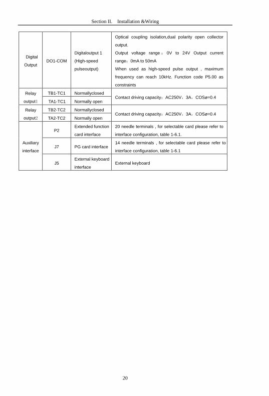
2.6 Control circuit terminals ...................................................................................... 18
2.6.1 Control circuit terminal arrangement ......................................................... 18
2.6.2 Control circuit terminals description .......................................................... 19
2.6.3 Description of wiring of control terminals .................................................. 21
2.7 Standby circuit .................................................................................................... 23
Section III. Fittings ............................................................................................................. 24
3.1 Connection with peripheral devices .............................................................................. 24
3.1.1 Connection of the Product and Peripheral Devices .......................................... 24

3.1.2 Peripheral Electric Parts of HV590 .................................................................... 25
3.2 Mounting hole dimension ................................................................................................ 27
3.2.1 Braking unit & Braking resistance ...................................................................... 27
3.2.2 Specifications of circuit breaker、cable and contactors ................................ 28
Section IV. Keyboard Operation ........................................................................................ 29
4.1 Keyboard size ................................................................................................................... 29
4.1.1 HV590 keyboard specification ............................................................................ 29
4.1.2 Keyboard warehouse JP3 dimension ............................................................... 29
4.2 Display Interface .............................................................................................................. 30
4.2.1 Function description of operation panel ............................................................ 30
4.3 Examples for parameter setting .................................................................................... 32
4.3.1 Description of function code viewing and modificationmethod ..................... 32
4.3.2 Parameter display mode ..................................................................................... 32
4.3.3 User set parameter operation mode ................................................................. 33
4.3.4 Check method of state parameter ..................................................................... 34
4.3.5 Password Setting .................................................................................................. 34
4.3.6 Motor parameter automatic tuning ..................................................................... 35
4.4 Test running ...................................................................................................................... 36
Section V. Parameter Function Table ............................................................................... 37
5.1 Monitor function group:U0.00-U0.61 ......................................................................... 37
5.2 Basic function group:P0.00-P0.28.............................................................................. 42
5.3 Parameters for motor 1:P1.00-P1.37 ......................................................................... 51
5.4 Vector control function group:P2.00-P2.22 .............................................................. 53
5.5 V/F control group:P3.00-P3.15 ................................................................................... 55
5.6 Input terminal:P4.00-P4.40 .......................................................................................... 59

5.7 Output terminal:P5.00-P5.22 ...................................................................................... 72
5.8 Start/stop control:P6.00-P6.15 ................................................................................... 76
5.9 Keyboard and display:P7.00-P7.14 ........................................................................... 80
5.10 Auxiliary function:P8.00-P8.53 ................................................................................. 83
5.11 Overload and protection:P9.00-P9.70..................................................................... 91
5.12 PID function group:PA.00-PA.28 ........................................................................... 100
5.13 Swing frequency, fixed length and counting:Pb.00-Pb.09 ................................. 104
5.14 MS speed function&simple PLC function:PC.00-PC.51 .................................... 106
5.15 Communication function group:Pd.00-Pd.06 ....................................................... 110
5.16 User customization function code:PE.00-PE.29 ................................................. 111
5.17 Function code management:PP.00-PP.04 ........................................................... 112
5.18 Torque control group: A0.00-A0.08 ...................................................................... 114
5.19 VirtualIO: A1.00-A1.21 ............................................................................................ 115
5.20 The second motor control:A2.00-A2.65 ................................................................ 119
5.21 The third motor control: A5.00-A5.09 ................................................................... 122
5.22 AI curve setup: A6.00-A6.29 .................................................................................. 123
5.23 User programmable card parameters: A7.00-A7.09 ......................................... 125
5.24 Point to point communication:A8.00-8.11 ............................................................ 126
5.25 Extended function group:A9.00-A9.09 .................................................................. 127
5.26 AI/AO correction: AC.00-AC.19 ............................................................................. 127
Section VI. Fault Diagnosis & Solutions ........................................................................ 129
6.1 Fault alarm and solutions ............................................................................................. 129
6.2 Common fault and solutions ........................................................................................ 136
Section VII. Inspection & Maintenance .......................................................................... 147
7.1 Inspection and Maintenance ........................................................................................ 147
7.2 Regular replacement of the device ............................................................................. 148
7.3 Storage ............................................................................................................................ 148
7.4 Measuring and Judgment ............................................................................................. 148
7.5 Safety Precaution ........................................................................................................... 148
Appendix I. H5RS485 Card & RS485Communication Protocol .................................... 149
I.1 H5RS485 card ................................................................................................................. 149
I.2 Communication protocol ................................................................................................ 149
I.2.1 Protocol content ................................................................................................... 149
I.3 Protocol Description........................................................................................................ 149
I.4 Cyclical Redundancy Check ......................................................................................... 152
Appendix II. Parameter Settings List .............................................................................. 160
Appendix III. Recommended accessories selection ..................................................... 181
1.Brake unit braking resistor selection: ............................................................................. 181
2.Input AC reactor................................................................................................................. 182
3.Output AC reactor ............................................................................................................. 183
Product Feedback .............................................................................................................. 185
Warranty Agreement ........................................................................................................... 186
1
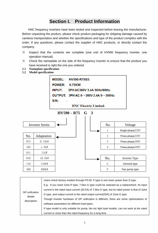
Section I. Product Information
HNC frequency inverters have been tested and inspected before leaving the manufacturer.
Before unpacking the product, please check product packaging for shipping damage caused by
careless transportation and whether the specifications and type of the product complies with the
order. If any questions, please contact the supplier of HNC products, or directly contact the
company.
※ Inspect that the contents are complete (one unit of HV590 frequency inverter, one
operation manual).
※ Check the nameplate on the side of the frequency inverter to ensure that the product you
have received is right the one you ordered.
1.1 Nameplate specification
1.2 Model specification
HV590 – R75 G 3
Inverter Series No. Voltage
1 Single-phase220V
No. Adaptation 2 Three-phase220V
R75 0.75kW 3 Three-phase380V
1R5 1.5kW
4 Three-phase480V
011 11kW
018 18.5kW No. Inverter Type
110 110kW G General type
400 400kW P Fan pump type
GP unification
Model
description
Users check factory models through P0.00. P type is one lower power than G type.
E.g:If you need 11kw P type, 7.5kw G type could be selected as a replacement. Its input
current is the rated input current (20.5A) of 7.5kw G type, but its rated power is that of 11kw
G type, and output current is the rated output current(25A) of 11kw G type.
Though inverter hardware of GP unification is different, there are some optimizations of
software parameters for different load types .
P type model is only suitable for pump, fan etc light load models, can not work at the rated
current or more than the rated frequency for a long time.

Section I. Product Information
2
1.3 Product series
Inverter model Motor adapter
Rated input A Rated output A kW HP
1PH single phase input:AC 220V,50/60Hz
HV590-R40G1 0.4 0.5 5.9 2.5
HV590-R75G1 0.75 1 8.3 4
HV590-1R5G1 1.5 2 14.1 7
HV590-2R2G1 2.2 3 24.2 10
HV590-004G1 4.0 5.5 34.0 16
3PH 3-phase input:AC 220V,50/60Hz
HV590-R40G2 0.4 0.5 4.1 2.5
HV590-R75G2 0.75 1 5.3 4
HV590-1R5G2 1.5 2 8.0 7
HV590-2R2G2 2.2 3 11.8 10
HV590-004G2 4.0 5.5 18.1 16
HV590-5R5G2 5.5 7.5 28.0 25
HV590-7R5G2 7.5 10 37.1 32
HV590-011G2 11 15 49.8 45
HV590-015G2 15 20 65.4 60
HV590-018G2 18.5 25 81.6 75
HV590-022G2 22 30 97.7 90
HV590-030G2 30 40 122.1 110
HV590-037G2 37 50 157.4 152
HV590-045G2 45 60 185.3 176
HV590-055G2 55 70 215.8 210
3PH 3-phase input:AC 380V,50/60Hz
HV590-R75G3 0.75 1 4.3 2.5
HV590-1R5G3 1.5 2 5.2 3.7
HV590-2R2G3 2.2 3 6.0 5
HV590-004G3 4.0 5 10.5 8.5
HV590-5R5G3 5.5 7.5 15.5 13
HV590-7R5G3 7.5 10 20.5 16
HV590-011G3 11.0 15 27.5 25
HV590-015G3 15.0 20 37.1 32
HV590-018G3 18.5 25 41.9 38
HV590-022G3 22 30 49.3 45

Section I. Product Information
3
HV590-030G3 30 40 65.7 60
HV590-037G3 37 50 80.6 75
HV590-045G3 45 60 96.4 90
HV590-055G3 55 70 117.6 110
HV590-075G3 75 100 166.4 150
HV590-093G3 90 125 184.3 170
HV590-110G3 110 150 226.8 210
HV590-132G3 132 175 268.1 250
HV590-160G3 160 210 321.1 300
HV590-187G3 185 245 368.0 340
HV590-200G3 200 260 406.6 380
HV590-220G3 220 300 442.7 415
HV590-250G3 250 350 503.0 470
HV590-280G3 280 370 555.9 520
HV590-315G3 315 500 650.7 600
HV590-355G3 355 420 734.5 650
HV590-400G3 400 530 787.6 725
HV590-450G3 450 595 846.0 820
HV590-500G3 500 670 885.0 860
HV590-560G3 560 750 990.0 950
HV590-630G3 630 840 1150.0 1100
3PH 3-phase input:AC 460V,50/60Hz
HV590-R75G4 0.75 1 4.1 2.5
HV590-1R5G4 1.5 2 4.9 3.7
HV590-2R2G4 2.2 3 5.7 5
HV590-004G4 4.0 5 9.4 8
HV590-5R5G4 5.5 7.5 12.5 11
HV590-7R5G4 7.5 10 18.3 15
HV590-011G4 11.0 15 23.1 22
HV590-015G4 15.0 20 29.8 27
HV590-018G4 18.5 25 35.7 34
HV590-022G4 22 30 41.7 40
HV590-030G4 30 40 57.4 55
HV590-037G4 37 50 66.5 65
HV590-045G4 45 60 81.7 80
HV590-055G4 55 70 101.9 100
HV590-075G4 75 100 137.4 130
HV590-093G4 90 125 151.8 147
Section I. Product Information
4
HV590-110G4 110 150 216.0 180
HV590-132G4 132 175 220.7 216
HV590-160G4 160 210 264.2 259
HV590-187G4 185 245 309.4 300
HV590-200G4 200 260 334.4 328
HV590-220G4 220 300 363.9 358
HV590-250G4 250 350 407.9 400
HV590-280G4 280 370 457.4 449
HV590-315G4 315 500 533.2 516
HV590-355G4 355 420 623.3 570
HV590-400G4 400 530 706.9 650
HV590-450G4 450 595 760.0 700
HV590-500G4 500 670 865.0 800
HV590-560G4 560 750 970.0 900
HV590-630G4 630 840 1100.0 1000
Table 1-3
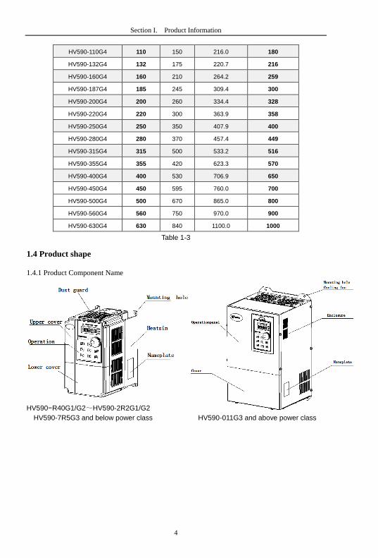
1.4 Product shape
1.4.1 Product Component Name
HV590−R40G1/G2~HV590-2R2G1/G2
HV590-7R5G3 and below power class HV590-011G3 and above power class
Section I. Product Information
5
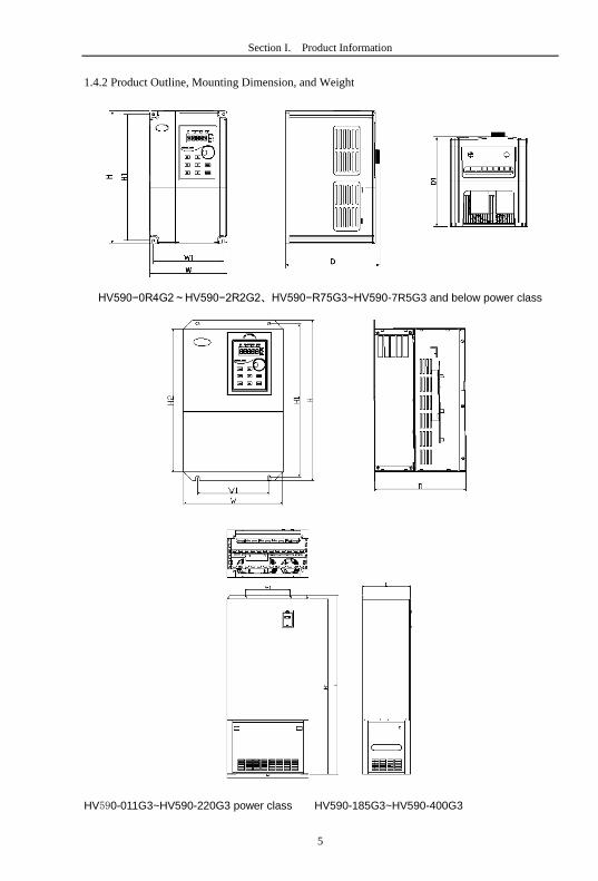
1.4.2 Product Outline, Mounting Dimension, and Weight
HV590−0R4G2~HV590−2R2G2、HV590−R75G3~HV590-7R5G3 and below power class
HV590-011G3~HV590-220G3 power class HV590-185G3~HV590-400G3

Section I. Product Information
6
Fig.1−4 Product outline and mounting dimension
Shape DIM
Shape dimension and nstallation dimension(mm)
Weight
(kg
) W H D W1 H1 D1 H2
Asse
mbly
apert
ure
HV590−R40G1
118.5 185 159 106.5 174.5 150 5.5 2.2 HV590−R75G1
HV590−1R5G1
HV590−2R2G1
HV590-004G1 150 258 183.8 136.8 245 175.3 5.5 4.0
HV590−R40G2
118.5 185 159 106.5 174.5 150 5.5 2.2 HV590−R75G2
HV590−1R5G2
HV590−2R2G2
HV590-004G2 150 258 183.8 136.8 245 175.3 5.5 4.0
HV590-5R5G2 210 337 191 150 322.5 298 7 8.7
HV590-7R5G2 210 337 191 150 322.5 298 7 8.7
HV590-011G2 221 380 229.6 163 363.6 341 7 10
HV590-015G2 221 380 229.6 163 363.6 341 7 10
HV590-018G2 285 501 230.2 200 482 460 7 19
HV590-022G2 352 585 274.2 220 559 538 10 35
HV590-030G2 352 585 274.2 220 559 538 10 35
HV590−037G2 352 585 274.2 220 559 538 10 35
HV590−045G2 384 650 310 300 628 600 10 48
HV590−055G2 485 760 316 325 739 713 12 66
HV590−R75G3
118.5 185 159 106.5 174.5 150 5.5 2.2 HV590-1R5G3
HV590-2R2G3
HV590-004G3 118.5 195 169 106.5 184.5 160 5.5 2.6
HV590-5R5G3 150 258 183.8 136.8 245
175.
3 5.5 4.0
HV590-7R5G3
HV590-011G3 210 337 191 150 322.5 298 7 8.7
HV590-015G3
HV590-018G3 221 380 229.6 163 363.6 341 7 10
HV590-022G3
HV590-030G3 285 501 230.2 200 482 460 7 19
HV590−037G3
HV590−045G3
352 585 274.2 220 559 538 10 25 HV590−055G3
HV590−075G3
HV590−090G3 384 650 310 300 628 600 10 48
HV590−110G3 485 760 316 325 739 713 12 66
Wall mounting 533 830 405 325 809 780 12 94
Section I. Product Information
7
HV590−132G3
HV590−160G3
HV590−185G3
Cabinet installation
533 1212 405 325 1191 780 12 150 HV590−132G3
HV590−160G3
HV590−185G3
Cabinet installation
638 1402 374 350 1372 14 175 HV590−200G3
HV590−220G3
Cabinet installation
700 1627 460 520 1592 14 253 HV590−250G3
HV590−280G3
HV590−315G3
HV590−355G3 800 1772 460 520 1737 14 300
HV590−400G3
HV590−450G3
1200 2000 568 14 400 HV590−500G3
HV590−560G3
HV590−630G3
HV590−R75G4
118.5 185 159 106.5 174.5 150 5.5 2.2 HV590-1R5G4
HV590-2R2G4
HV590-004G4 118.5 195 169 106.5 184.5 160 5.5 2.6
HV590-5R5G4 150 258 183.8 136.8 245
175.
3 5.5 4.0
HV590-7R5G4
HV590-011G4 210 337 191 150 322.5 298 7 8.7
HV590-015G4
HV590-018G4 221 380 229.6 163 363.6 341 7 10
HV590-022G4
HV590-030G4 285 501 230.2 200 482 460 7 19
HV590−037G4
HV590−045G4
352 585 274.2 220 559 538 10 25 HV590−055G4
HV590−075G4
HV590−090G4 384 650 310 300 628 600 10 48
HV590−110G4 485 760 316 325 739 713 12 66
Wall mounting
533 830 405 325 809 780 12 94 HV590−132G4
HV590−160G4
HV590−185G4
Cabinet installation
533 1212 405 325 1191 780 12 150 HV590−132G4
HV590−160G4

Section I. Product Information
8
HV590−185G4
Cabinet installation
638 1402 374 350 1372 14 175 HV590−200G4
HV590−220G4
Cabinet installation
700 1627 460 520 1592 14 253 HV590−250G4
HV590−280G4
HV590−315G4
HV590−355G4 800 1772 460 520 1737 14 300
HV590−400G4
HV590−450G4
1200 2000 568 14 400 HV590−500G4
HV590−560G4
HV590−630G4

Section I. Product Information
9
1.5 Standard specification
Item Specifications
Ba
sic
fu
nc
tio
n
Control system High performance of current vector control technology to realize
asynchronous motor and synchronous motor control
Drive performance High efficiency driving for induction motor and synchronous motor
Maximum frequency Vector control:0~300HzV/Fcontrol:0~3200Hz
Carrier frequency 0.5k~16kHz;thecarrierfrequency will be automatically adjusted
according to the load characteristics
Input frequency resolution Digital setting: 0.01Hz
Analog setting: maximum frequency ×0.025%
Control mode
Open loop vector control(SVC)
Closed loop vector control(FVC)
V/F control
Startuptorque Type G:0.5Hz/150%(SVC);0Hz/180%(FVC)
Speed range 1:100(SVC) Speed range
Speed stabilizing precision ±0.5%(SVC) Speed stabilizing precision
Torque control precision ±5%(FVC)
Over load capability G type: rated current 150% -1 minute, rated current 180% -3
seconds;
Torque boost Auto torque boost function;Manual torque boost 0.1%~30.0%
V/Fcurve LinearV/F,Multi-point V/Fand Square V/F curve (power of 1.2, 1.4, 1.6,
1.8, 2)
V/F separation In 2 ways:separation ,semi seperation
Acc. /deccurve
Straight line or S curve acceleration and deceleration mode.
Four kinds of acceleration and deceleration time. Acceleration and
deceleration time range between 0.0s to 6500.0s
DC brake DC brake frequency:0.00Hz to maximum frequency,brake time:
0.0s to 36.0s, and brake current value: 0.0% to 100.0%.
Jog control Jog frequency range:0.00Hz~50.00Hz. Jog acceleration/deceleration
time 0.0s~6500.0s.
Simple PLC and MS speed
running
It can realize at maximum of 16 segments speed running via the built-
in PLC or control terminal.
Built-in PID It is easy to realize process-controlled close loop control system
Auto voltage regulation
(AVR)
It can keep constant output voltage automatically in case of change of
network voltage.
Over-voltage/current stall
control
It can limit the running voltage/current automatically and prevent
frequent over-voltage/current tripping duringthe running process
Quickcurrent limit Minimize the over-current fault,protect normal operation of the inverter
Torque limit & control
"Excavators" characteristics,automatically limit torque during
operation,prevent frequent over-current trip;
Closed loop vector mode can realize the torque control.
Pers
on
alized
Instantaneous stop
non-stop
When instantaneous power off,voltage reduction is compensated
through load feedback energy,which could make inverter keep running
in a short period of time.
Rapid current limit To avoid inverter frequent over-current fault.
Virtual IO 5 groups of virtual DI,DO to realize simple logic control
Section I. Product Information
10
Timingcontrol Timing control function:settimerange0Min~6500.0Min
Multiple motor switch 4 groups of motor parameter,which can realize 4-motor switch control
Multi-threaded bus support Support 3 kinds of field bus:RS485, Profibus-DP, CANopen
Motor overheat protection Select optional H5PC1 analog input AI3x can accept the motor
temperature sensor input(PT100、PT1000)
Multi-encoder support Support difference,open collector, UVW, rotary transformer, sine
cosine encoder etc.
Programmable PLC Select optional user programmable card,which can realize secondary
development,programming mode compatible with Drino PLC.
Excellent backend software
Support inverter parameter operation and virtual oscilloscope
function.Inverter internal state graphic monitor can be realized
through virtual oscilloscope.
Ru
nn
ing
Running command channel
Three types of channels:operation panel reference,control terminal
reference and serial communication port reference.These channel
scan be switched in various modes.
Frequency source
There are totally eleven types of frequency sources, such as digital
reference, analog voltage reference, analog current reference, pulse
reference, MS speed, PLC, PID and serial port reference.
Auxiliary frequency source 11 kinds of auxiliary frequency source which can flexible achieve
auxiliary frequency tuning, frequency synthesis
Input terminal
Standard:
There are 6 digital input terminals,DI5 can be used as100kHz high-
speed input pulse.
2 analog input terminals which can be used as 0-10V voltage input or
0~20mA current input.
Extended function:
4 digital input terminals,
1analog input terminals support-10~10V voltage input &PT100\PT100
Output terminal
Standard:
1 digital output terminals, Y1 is high-speed pulse output terminal (can
be choosen as open circuit collector type), support 0~10kHz square
wave signal;
2 relay output terminal;
2 analog output terminals, support 0~20mA output current or 0~10V
output voltage;
Extended function:
2 digital output terminal;;
1 analog output terminal, support 0~20mA output current or 0~10V
output voltage.
Keyb
oard
op
era
tio
n
LED display Realizeparameter setting,statusmonitoringfunction
Keyboard potentiometer Equipped with keyboard potentiometer or coding potentiometer
Key lock&function selection Realize button locking,define operation range for part of buttons to
prevent operation fault.
Protection function
It can implement power-on motor short-circuit detection,input/output
phase loss protection, over current protection,over voltage
protection,under voltage protection,overheating protection and overload
protection.
Optionalparts Liquid crystal display operation panel, brake component, multi-
Section I. Product Information
11
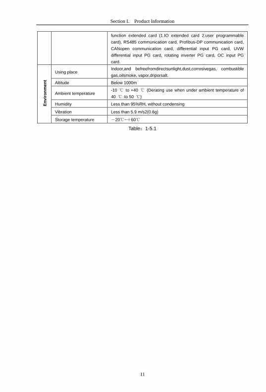
function extended card (1.IO extended card 2.user programmable
card), RS485 communication card, Profibus-DP communication card,
CANopen communication card, differential input PG card, UVW
differential input PG card, rotating inverter PG card, OC input PG
card.
En
vir
on
men
t
Using place Indoor,and befreefromdirectsunlight,dust,corrosivegas, combustible
gas,oilsmoke, vapor,driporsalt.
Altitude Below 1000m
Ambient temperature -10 to +40 (Derating use when under ambient temperature of
40 to 50 )
Humidity Less than 95%RH, without condensing
Vibration Less than 5.9 m/s2(0.6g)
Storage temperature -20~+60
Table:1-5.1
Section I. Product Information
12
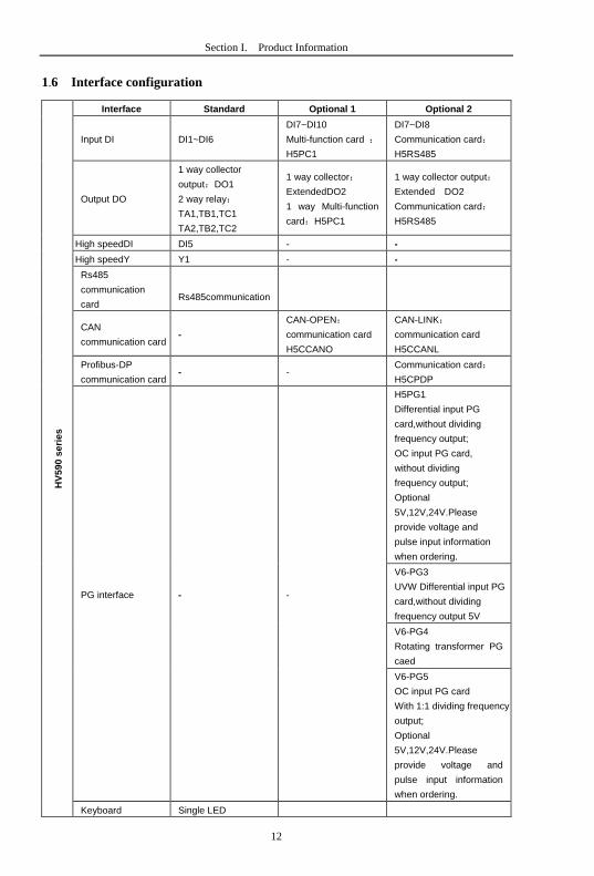
1.6 Interface configuration
HV
590 s
eri
es
Interface Standard Optional 1 Optional 2
Input DI DI1~DI6
DI7~DI10
Multi-function card :
H5PC1
DI7~DI8
Communication card:
H5RS485
Output DO
1 way collector
output:DO1
2 way relay:
TA1,TB1,TC1
TA2,TB2,TC2
1 way collector:
ExtendedDO2
1 way Multi-function
card:H5PC1
1 way collector output:
Extended DO2
Communication card:
H5RS485
High speedDI DI5 - -
High speedY Y1 - -
Rs485
communication
card
Rs485communication
CAN
communication card -
CAN-OPEN:
communication card
H5CCANO
CAN-LINK:
communication card
H5CCANL
Profibus-DP
communication card - -
Communication card:
H5CPDP
PG interface - -
H5PG1
Differential input PG
card,without dividing
frequency output;
OC input PG card,
without dividing
frequency output;
Optional
5V,12V,24V.Please
provide voltage and
pulse input information
when ordering.
V6-PG3
UVW Differential input PG
card,without dividing
frequency output 5V
V6-PG4
Rotating transformer PG
caed
V6-PG5
OC input PG card
With 1:1 dividing frequency
output;
Optional
5V,12V,24V.Please
provide voltage and
pulse input information
when ordering.
Keyboard Single LED

Section I. Product Information
13
keyboard:J5P1
6 groups of parameter
can be stored
Potentiometer
Constant pressure
water supply board -
4-pump constant
pressure water
supply
4-pump soft start
control panelH5WS
-
Table:1-6.1
If you need accessories in the table, please declare in order.
14
Section II. Installation &Wiring
2.1 Use of the environment
1) Ambient temperature-10~40.
2) Avoid electromagnetic interference and keep the unit away from the source of interference.
3) Prevent dropping water, steam, dust powder, cotton fiber or fine metal powderfrominvasion.
4) Prevent oil, salt and corrosive gas from entering it.
5) Avoid vibration. Vibration should be less than 0.6G. Keep away from punching machine etc.
6) Avoid high temperature, moisture or being wetted due to raining, with the humidity below
95%RH (non-condensing).
7) Prohibit the use in the dangerous environment where inflammable or combustible or explosive
gas, liquid or solid exists.
2.2 Handling and installation
※ When transporting inverter, right lifting tools are required to prevent inverter from
damaging.
※ The number of stacked box of the inverter are not permitted higher than the limit.
※ Please don’t run the inverter if there is damage or lacking of components.
※ Do not place heavy objects on the frequency inverter.
※ Please prevent screw, cable pieces or other conductive objects or oil etc
inflammableobjects invading the frequency inverter.
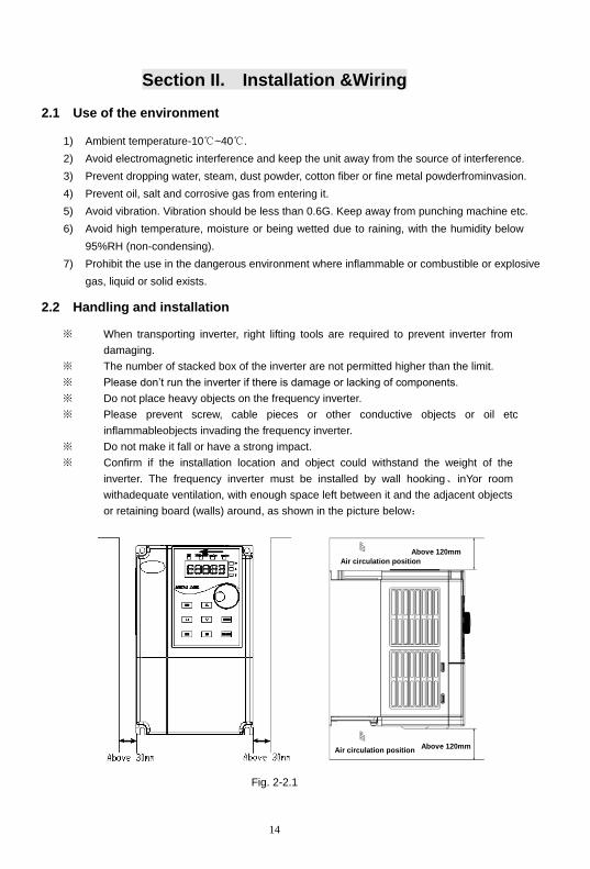
※ Do not make it fall or have a strong impact.
※ Confirm if the installation location and object could withstand the weight of the
inverter. The frequency inverter must be installed by wall hooking、inYor room
withadequate ventilation, with enough space left between it and the adjacent objects
or retaining board (walls) around, as shown in the picture below:
Fig. 2-2.1
Air circulation position
Air circulation position
Above 120mm
Above 120mm
Air circulation position
Air circulation position
Above 120mm
Above 120mm
Section II. Installation &Wiring
15
Heat dissipation problems should be concerned when doing mechanical installation, please
mind rules belows:
1) Mounting space is shown in 2-2.1, which could ensure the heat sinking space of the
inverter. However, the heat sinking of other devices in the cabinet shall also be considered.
2) Install the inverter vertically so that the heat may be expelled from the top.However, the
equipment cannot be installed upside down. If there are multiple inverters in the cabinet,
parallel installation is better. In the applications where up-down installation is required,
please install the thermal insulating guide plate referring to the Fig. 2-2.2 for standalone
installation and up-down installation.
3) Installing support must be flame retardant materials.
4) It is suggested that cooling cabinet be put outside at places where powder dust exists.
Space inside the sealed cabinet shall be large as much as possible.
Section II. Installation &Wiring
16
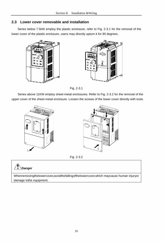
2.3 Lower cover removable and installation
Series below 7.5kW employ the plastic enclosure, refer to Fig. 2-3.1 for the removal of the
lower cover of the plastic enclosure, users may directly upturn it for 90 degrees.
Fig. 2-3.1
Series above 11KW employ sheet-metal enclosures. Refer to Fig. 2-3.2 for the removal of the
upper cover of the sheet-metal enclosure. Loosen the screws of the lower cover directly with tools.
Fig. 2-3.2
Danger
Whenremovingthelowercover,avoidthefallingofthelowercover,which maycause human injuryor
damage tothe equipment.
Section II. Installation &Wiring
17
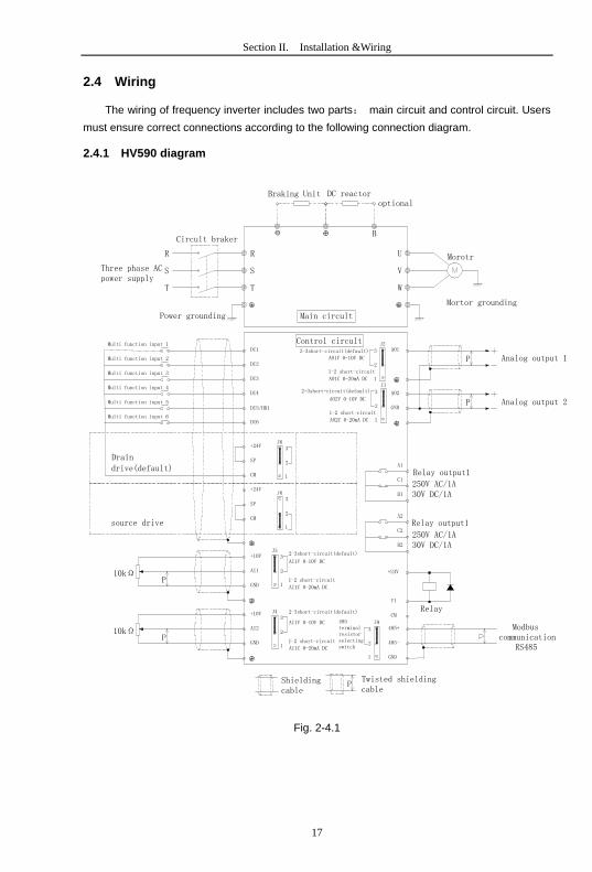
2.4 Wiring
The wiring of frequency inverter includes two parts: main circuit and control circuit. Users
must ensure correct connections according to the following connection diagram.
2.4.1 HV590 diagram
B
R
S
T
U
V
W
DI1
DI2
DI3
DI4
DI5/HD1
DI6
+10V
AI1
GND
10kΩP
AO1
AO2
GND
A1
+24V
Y1
P
P
C1
B1
250V AC/1A30V DC/1A
CM
P
R
S
T
A2
C2
B2
250V AC/1A30V DC/1A
+10V
AI2
GND
10kΩP
+24V
SP
CM
+24V
485+
485-
GND
SP
CM
3
2
1
J6
3
2
1
J6
Drain drive(default)
source drive
3
2
1
J32-3short-circuit(default)
AI1V 0-10V DC
1-2 short-circuit
AI1C 0-20mA DC
3
2
1
J4 2-3short-circuit(default)
AI1V 0-10V DC
1-2 short-circuit
AI1C 0-20mA DC
3
2
1
J2
2-3short-circuit(default)AO1V 0-10V DC
1-2 short-circuit
AO1C 0-20mA DC
3
2
1
2-3short-circuit(default)
AO2V 0-10V DC
1-2 short-circuit
AO2C 0-20mA DC
J1
3
2
1
J9485 terminal resistor selecting switch
Circult braker
Three phase ACpower supply
Power grounding
Braking Unit
Morotr
Mortor grounding
Multi function input 1
Multi function input 2
Multi function input 3
Multi function input 4
Multi function input 5
Multi function input 6
DC reactor
Main circult
Control circult
Analog output 1
Analog output 2
Relay output1
Relay output1
Relay
Modbuscommunication
RS485
Shieldingcable
Twisted shieldingcable
optional
Fig. 2-4.1
Section II. Installation &Wiring
18
2.5 Main circuit terminals (G type)
2.5.1 HV590 main circuit terminals
HV590−R40G2~HV590−004G2 & HV590−R75G3~HV590−015G3
2.5.2 HV550−018G3~HV550−630G3
Terminal symbol Terminal name and function description
R、S、T Three-phase AC input terminal
⊕1、⊕2 DC reactor connecting terminal, short circuited with copper bus upon
delivery ⊕2、 Ө DC power input terminal; DC input terminal of external braking unit
U、V、W Three-phase AC output terminal
Grounding terminal PE
2.6 Control circuit terminals
2.6.1 Control circuit terminal arrangement
HV590 Control circuit terminals
24V SP CM DI1 DI2 DI3 DI4 DI5 DI6 CM A2 B2 C2
+10VAI1 AI2 GND 485+ Y1 A1 B1 C1485-GNDAO2AO1
Terminal symbol Terminal name and function description
R、S、T Three-phase AC input terminal
⊕、B Connecting terminal of braking resistor
⊕、Ө DC power input terminal; DC input terminal of external braking unit
U、V、W Three-phase AC output terminal
Grounding terminal PE
Section II. Installation &Wiring
19
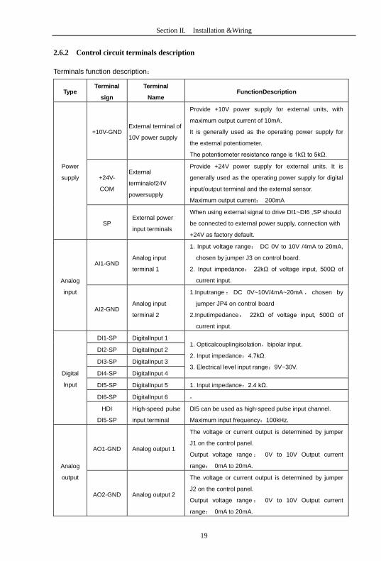
2.6.2 Control circuit terminals description
Terminals function description:
Type Terminal
sign
Terminal
Name FunctionDescription
Power
supply
+10V-GND External terminal of
10V power supply
Provide +10V power supply for external units, with
maximum output current of 10mA.
It is generally used as the operating power supply for
the external potentiometer.
The potentiometer resistance range is 1kΩ to 5kΩ.
+24V-
COM
External
terminalof24V
powersupply
Provide +24V power supply for external units. It is
generally used as the operating power supply for digital
input/output terminal and the external sensor.
Maximum output current: 200mA
SP External power
input terminals
When using external signal to drive DI1~DI6 ,SP should
be connected to external power supply, connection with
+24V as factory default.
Analog
input
AI1-GND Analog input
terminal 1
1. Input voltage range: DC 0V to 10V /4mA to 20mA,
chosen by jumper J3 on control board.
2. Input impedance: 22kΩ of voltage input, 500Ω of
current input.
AI2-GND Analog input
terminal 2
1.Inputrange : DC 0V~10V/4mA~20mA , chosen by
jumper JP4 on control board
2.Inputimpedance: 22kΩ of voltage input, 500Ω of
current input.
Digital
Input
DI1-SP DigitalInput 1 1. Opticalcouplingisolation,bipolar input.
2. Input impedance:4.7kΩ.
3. Electrical level input range:9V~30V.
DI2-SP DigitalInput 2
DI3-SP DigitalInput 3
DI4-SP DigitalInput 4
DI5-SP DigitalInput 5 1. Input impedance:2.4 kΩ.
DI6-SP DigitalInput 6 -
HDI
DI5-SP
High-speed pulse
input terminal
DI5 can be used as high-speed pulse input channel.
Maximum input frequency:100kHz.
Analog
output
AO1-GND Analog output 1
The voltage or current output is determined by jumper
J1 on the control panel.
Output voltage range : 0V to 10V Output current
range: 0mA to 20mA.
AO2-GND Analog output 2
The voltage or current output is determined by jumper
J2 on the control panel.
Output voltage range : 0V to 10V Output current
range: 0mA to 20mA.
Section II. Installation &Wiring
20
Digital
Output DO1-COM
Digitaloutput 1
(High-speed
pulseoutput)
Optical coupling isolation,dual polarity open collector
output.
Output voltage range : 0V to 24V Output current
range:0mA to 50mA
When used as high-speed pulse output , maximum
frequency can reach 10kHz. Function code P5.00 as
constraints
Relay
output1
TB1-TC1 Normallyclosed Contact driving capacity:AC250V,3A,COSø=0.4
TA1-TC1 Normally open
Relay
output2
TB2-TC2 Normallyclosed Contact driving capacity:AC250V,3A,COSø=0.4
TA2-TC2 Normally open
Auxiliary
interface
P2 Extended function
card interface
20 needle terminals , for selectable card please refer to
interface configuration, table 1-6.1.
J7 PG card interface 14 needle terminals , for selectable card please refer to
interface configuration, table 1-6.1
J5 External keyboard
interface External keyboard

Section II. Installation &Wiring
21
2.6.3 Description of wiring of control terminals
1) Analoginput terminal
Because the weak analog signal will be easily affected by the external interference,
generally shielded cable shall be used, the cable length shall be as short as possible and no
longer than 20 meters, as shown in Fig. 2-6.1. In case the analog signal is subject to severe
interference, analog signal source side shall be installed with filter capacitor or ferrite magnetic
ring, as shown in Fig.2-6.2.
Fig. 2-6.1 Analog input terminal wiring diagram
Fig.2-6.2Analog input terminal processing wiring diagram
Less then 20 meters
+10V
AI1
GND
PE
HV590
AI1
GND
HV590
Ferriter magnetic ring
0.022uF
C
Go through in the same direction or
wind 2~3 rounds in the same direction
External analog source
Section II. Installation &Wiring
22
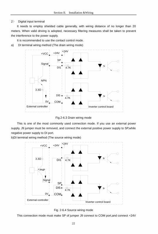
2) Digital input terminal
It needs to employ shielded cable generally, with wiring distance of no longer than 20
meters. When valid driving is adopted, necessary filtering measures shall be taken to prevent
the interference to the power supply.
It is recommended to use the contact control mode.
a) DI terminal wiring method (The drain wiring mode)
Fig.2-6.3 Drain wiring mode
This is one of the most commonly used connection mode. If you use an external power
supply, J9 jumper must be removed, and connect the external positive power supply to SP,while
negative power supply to DI port.
b)DI terminal wiring method (The source wiring mode)
Fig. 2-6.4 Source wiring mode
This connection mode must make SP of jumper J9 connect to COM port,and connect +24V
External controller Inverter control board
NPN
3.3Ω
0V COM
DI54.7K
Signal
+VCC +24V
DI1
SP
4.7K
+24V
External controllerInverter control board
PNP
3.3Ω
0V COM
DI54.7K
Signal
+VCC +24V
DI1
SP
4.7K
+24V
Section II. Installation &Wiring
23
and public terminal of external controller together.If you use an external power supply,jumper J9
must be removed,and connect external negative power supply to SP ,while positive power
supply to DI port.
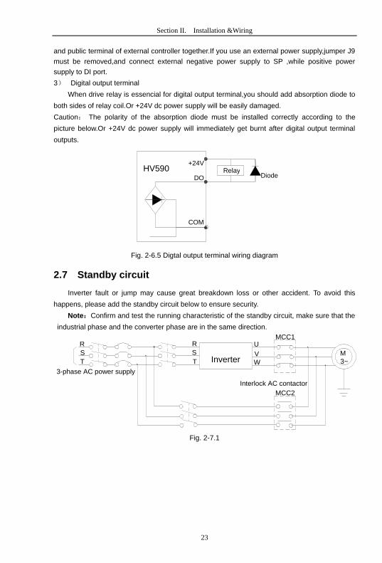
3) Digital output terminal
When drive relay is essencial for digital output terminal,you should add absorption diode to
both sides of relay coil.Or +24V dc power supply will be easily damaged.
Caution: The polarity of the absorption diode must be installed correctly according to the
picture below.Or +24V dc power supply will immediately get burnt after digital output terminal
outputs.
Fig. 2-6.5 Digtal output terminal wiring diagram
2.7 Standby circuit
Inverter fault or jump may cause great breakdown loss or other accident. To avoid this
happens, please add the standby circuit below to ensure security.
Note:Confirm and test the running characteristic of the standby circuit, make sure that the
industrial phase and the converter phase are in the same direction.
Fig. 2-7.1
T
R
SInverter
R
Interlock AC contactor
3-phase AC power supply
M
3~T
S
U
V
W
MCC1
MCC2
Relay
COM
+24V
DO
HV590 Diode

24
Section III. Fittings
3.1 Connection with peripheral devices
3.1.1 Connection of the Product and Peripheral Devices
Fig.3−1 Connection diagram of the product and peripheral devices
Power supply
Contactor
Input AC reactor
DC reactor
Inverter
Grounding
Motor
Circuit breaker or
leakage circuit breaker
Input noise filter
Output noise filter
Braking resistor
Output AC reactor

Section IV. Keyboard Operation
25
3.1.2 Peripheral Electric Parts of HV590
PartName InstallationLocation FunctionDescription
Circuit breaker The front-end of
theinputcircuit
Disconnect the power supply in case of downstream
equipment is over current
Contactor Between the circuitbreaker
andthe inverterinputside
Power-onandpower-offoftheinverter.Frequent
power-on/power-off operation(at least once per
minute) on the inverter should be avoided
AC input reactor Inputsideof the inverter
Improve the power factor of the input side:
1.Eliminate the high order harmonics of the input
side effectively, and prevent other equipment from
damagingdue to voltage waveform deformation.
2.Eliminate the unbalancedinput current due to
theunbalancedpowerphases.
EMC input filter Input side ofthe inverter
1.Reduce the external conduction and radiation
interference of the inverter;
2.Reduce the conduction interference flowing from
thepower end to the inverter, thus improving the
anti-interference capacity of the inverter.
3.The common size of 3-phase EMI noise filter is
shown as following: confirm the power supply is
3-phase three lines or 3-phase four lines or single
phase. Grounding wire is as short as possible, try
to place the filter near the converter.
Please choose EMI filter when the inverter is used
in residential area, commercial area, science area
as well as situations where higher demand to
prevent radio interference is needed or meeting
CE、UL、CSA standard but existing equipment that
anti-interference ability is not sufficient.
If needing the filter, please connect with the company.
DC reactor
HV590 series can adopt
external DC reactor
according to the need.
Improve the power factor of the input side:
1.Improve the overall efficiency and thermal stability
2.Effectively reduce the influence of high order
harmonicsat the input side on the inverter and
reduce the external conduction and radiation
interference.
ACoutput reactor
Between the inverter output
side and the
motor,closetothe inverter
The inverter output side generally has higher
harmonic.When the motor is far from the inverter,
since there are many capacitors in the circuit,
certain harmonics will cause resonance in the circuit
and bring in the following results:
1.Degrade the motor insulation performance and
damagethe motor for the long run
2.Generatelarge leakage current and cause frequent

Section IV. Keyboard Operation
26
inverter protection action
3.In general, if the distance between the inverter
and themotor exceeds 100 meters, output AC
reactor should be installed
Output EMI filter
Between the inverter output
side and the motor,closetothe
inverter
The fittings can restrain the disturbance noise and
lead line leak current produced in the output side.
Table:3-1.1

Section IV. Keyboard Operation
27
3.2 Mounting hole dimension
3.2.1 Braking unit & Braking resistance
When customers choose the type with braking,there will be braking unit inside the
inverter,maximum braking torque is 50%.Please refer to the table below and choose the matched
braking resistance separately.
Shape DIM Braking
unit
Braking unit
Braking moment % Braking
Quanti
ty
HV590−R40G1/G2
Standard
built-in
100W 300Ω 1 220
HV590−R75G1/G2 120W 200Ω 1 125
HV590−1R5G1/G2 300W 100Ω 1 125
HV590−2R2G1/G2 300W 70Ω 1 120
HV590−R75G3 100W 300Ω 1 130
HV590−1R5G3 200W 300Ω 1 125
HV590−2R2G3 200W 200Ω 1 135
HV590−3R7G3 400W 150Ω 1 135
HV590−5R5G3 500W 100Ω 1 135
HV590−7R5G3 800W 75Ω 1 130
HV590−011G3 1040W 50Ω 1 135
HV590−015G3 1560W 40Ω 1 125
HV590−018G3 4800W 32Ω 1 125
HV590−022G3 4800W 27.2Ω 1 125
HV590−030G3
outlay
6000W 20Ω 1 125
HV590−037G3 9600W 16Ω 1 125
HV590−045G3 9600W 13.6Ω 1 125
HV590−055G3 6000W 20Ω 2 135
HV590−075G3 9600W 13.6Ω 2 145
Table:3-2.1
If you need accessories in the table,please declare in order.
For larger built-in braking torque,please use the HNC braking unit.do ou can refer to HNC
braking unit manual for details.
Other large power models do not contain a built-in braking.If large power model need to be
equipped with braking function,please choose HNC braking unit.
External DC reactor installation:
For HV590 series inverter, external DC reactor can be ordered according to your
needs.When installation,you should tear down copper platoon between DC+1 and DC+2 of
inverter main circuit.And then add reactor between DC+1 and DC+2,wiring between reactor
terminals and inverter terminals DC+1 and DC+2 have no polarity. After installation of dc
reactor,short circuit copper platoon between DC+1 and DC+2 is no more used.

Section IV. Keyboard Operation
28
3.2.2 Specifications of circuit breaker、cable and contactors
Shape DIM breaker
(A)
contacto
r(A)
R、S、T、⊕、B、Ө、U、V、W Terminal screwPE
Termina
l screw
FasteningMo
ment(N·m)
wiresta
ndard(
mm2)
Termina
l screw
FasteningMo
ment(N·m)
wiresta
ndard(
mm2)
HV590−R40G1/G2 16 10 M4 1.2~1.5 2.5 M4 1.2~1.5 2.5
HV590−R75G1/G2 25 16 M4 1.2~1.5 2.5 M4 1.2~1.5 2.5
HV590−1R5G1/G2 32 25 M4 1.2~1.5 4 M4 1.2~1.5 2.5
HV590−2R2G1/G2 40 32 M4 1.2~1.5 6 M4 1.2~1.5 4
HV590−R75G3 10 10 M4 1.2~1.5 2.5 M4 1.2~1.5 2.5
HV590−1R5G3 16 10 M4 1.2~1.5 2.5 M4 1.2~1.5 2.5
HV590−2R2G3 16 10 M4 1.2~1.5 2.5 M4 1.2~1.5 2.5
HV590−3R7G3 25 16 M4 1.2~1.5 4 M4 1.2~1.5 4
HV590−5R5G3 32 25 M4 1.2~1.5 6 M4 1.2~1.5 6
HV590−7R5G3 40 32 M4 1.2~1.5 6 M4 1.2~1.5 6
HV590−011G3 63 40 M5 2.5~3.0 6 M5 2.5~3.0 6
HV590−015G3 63 63 M5 2.5~3.0 6 M5 2.5~3.0 6
HV590−018G3 100 63 M6 4.0~5.0 10 M6 4.0~5.0 10
HV590−022G3 100 100 M6 4.0~5.0 16 M6 4.0~5.0 16
HV590−030G3 125 100 M6 4.0~5.0 25 M6 4.0~5.0 16
HV590−037G3 160 100 M8 9.0~10.0 25 M8 9.0~10.0 16
HV590−045G3 200 125 M8 9.0~10.0 35 M8 9.0~10.0 16
HV590−055G3 315 250 M10 17.6~22.5 50 M10 14.0~15.0 25
HV590−075G3 350 330 M10 17.6~22.5 60 M10 14.0~15.0 35
HV590−090G3 315 250 M10 17.6~22.5 70 M10 14.0~15.0 35
HV590−110G3 350 330 M10 17.6~22.5 100 M10 14.0~15.0 50
HV590−132G3 400 330 M12 31.4~39.2 150 M12 17.6~22.5 75
HV590−160G3 500 400 M12 31.4~39.2 185 M12 17.6~22.5 50×2
HV590−200G3 630 500 M12 48.6~59.4 240 M12 31.4~39.2 60×2
HV590−220G3 800 630 M12 48.6~59.4 150×2 M12 31.4~39.2 75×2
HV590−280G3 1000 630 M12 48.6~59.4 185×2 M12 31.4~39.2 100×2
HV590−315G3 1000 800 M14 48.6~59.4 250×2 M14 31.4~39.2 125×2
HV590−355G3 1200 800 M14 48.6~59.4 325×2 M14 31.4~39.2 150×2
HV590−400G3 1500 1000 M14 48.6~59.4 325×2 M14 31.4~39.2 150×2
Table:3-2.3

Section IV. Keyboard Operation
29
Section IV. Keyboard Operation
4.1 Keyboard size
4.1.1 HV590 keyboard specification
Fig. 4-1.1
4.1.2 Keyboard warehouse JP3 dimension
Fig. 4-1.2
50.000
Section IV. Keyboard Operation
30
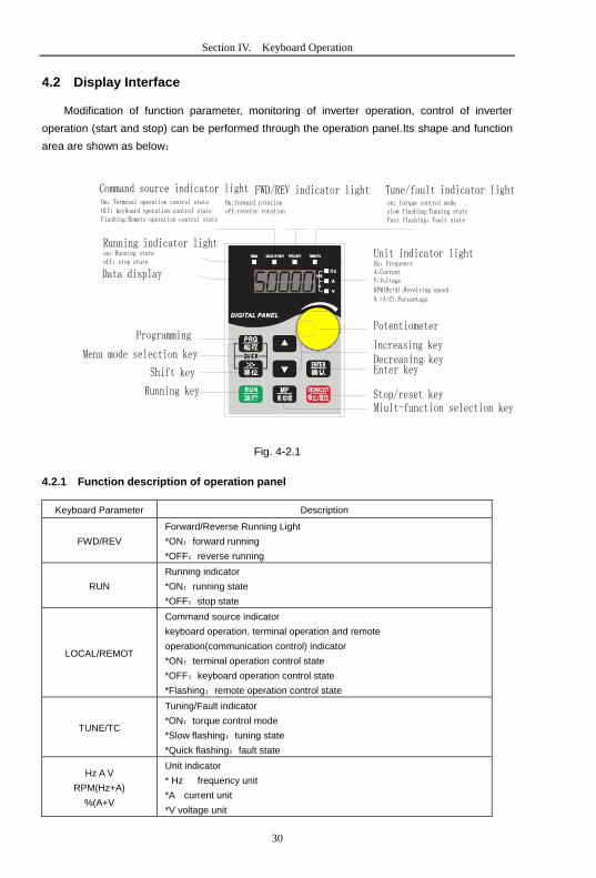
4.2 Display Interface
Modification of function parameter, monitoring of inverter operation, control of inverter
operation (start and stop) can be performed through the operation panel.Its shape and function
area are shown as below:
Data display
Running indicator lighton:Running stateoff:stop state
Command source indicator lightOn:Terminal operation control stateOff:keyboard operation control stateFlashing:Remote operation control state
FWD/REV indicator light Tune/fault indicator lighton:torque control modeslow flashing:Tunning stateFast flashing:Fault state
Unit indicator lightHz:FrequencyA:CurrentV:VoltageRPM(Hz+A):Revolving speed%(A+Z):Percentage
Potentiometer
Increasing keyDecreasing keyEnter key
Stop/reset keyMiult-function selection key
Programming
Menu mode selection key
Shift key
Running key
On:forward rotationoff:reverse rotation
Fig. 4-2.1
4.2.1 Function description of operation panel
Keyboard Parameter Description
FWD/REV
Forward/Reverse Running Light
*ON:forward running
*OFF:reverse running
RUN
Running indicator
*ON:running state
*OFF:stop state
LOCAL/REMOT
Command source indicator
keyboard operation, terminal operation and remote
operation(communication control) indicator
*ON:terminal operation control state
*OFF:keyboard operation control state
*Flashing:remote operation control state
TUNE/TC
Tuning/Fault indicator
*ON:torque control mode
*Slow flashing:tuning state
*Quick flashing:fault state
Hz A V
RPM(Hz+A)
%(A+V
Unit indicator
* Hz frequency unit
*A current unit
*V voltage unit
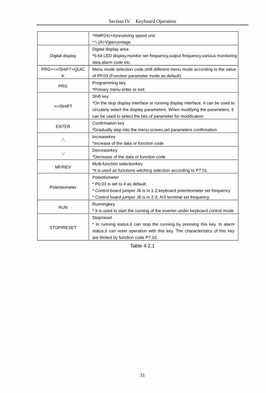
Section IV. Keyboard Operation
31
*RMP(Hz+A)revolving speed unit
*%(A+V)percentage
Digital display
Digital display area
*5-bit LED display,monitor set frequency,output frequency,various monitoring
data,alarm code etc.
PRG+>>/SHIFT=QUIC
K
Menu mode selection code,shift different menu mode according to the value
of PP.03 (Function parameter mode as default)
PRG Programming key
*Primary menu enter or exit
>>/SHIFT
Shift key
*On the stop display interface or running display interface, it can be used to
circularly select the display parameters. When modifying the parameters, it
can be used to select the bits of parameter for modification
ENTER Confirmation key
*Gradually step into the menu screen,set parameters confirmation
∧ Increasekey
*Increase of the data or function code
∨ Decreasekey
*Decrease of the data or function code
MF/REV Multi-function selectionkey
*It is used as functions witching selection according to P7.01.
Potentiometer
Potentiometer
* P0.03 is set to 4 as default;
* Control board jumper J6 is in 1-2,keyboard potentiometer set frequency
* Control board jumper J6 is in 2-3, AI3 terminal set frequency
RUN Runningkey
* It is used to start the running of the inverter under keyboard control mode
STOP/RESET
Stop/reset
* In running status,it can stop the running by pressing this key. In alarm
status,it can reset operation with this key. The characteristics of this key
are limited by function code P7.02.
Table 4-2.1

Section IV. Keyboard Operation
32
4.3 Examples for parameter setting
4.3.1 Description of function code viewing and modificationmethod
The operation panel of HV590 inverter adopts three-level menu structure to perform
parameter setting.The three-level menu includes:function parameter group(level1menu)→
function code(level 2 menu)→setting value of function code(level 3 menu).The operation
process is as shown in Figure below.
Table 4-3.1
Caution: When operating on level 3 menu, press PRG key or ENTER key to return to level
2 menu. The difference between ENTER and PRG keys is that pressing ENTER KEY will
save the setup parameter and return to level 2 menu and then automatically shift to the next
function code, while pressing PRG key will directly return to level 2 menu without saving the
parameter, and it will return to the current function code.
Take the modification of function code P3.02(ranging from 10.00Hz to 15.00Hz ) as an
example. (The boldface bit indicates the flashing bit).
Table 4-3.2
In level 3 menu, if the parameter has no flashing bit, it indicates that the function code
cannot be modified. The possible reasons include:
1) The function code is an unchangeable parameter, such as actual detection parameter,
running record parameter, etc.
2) The function code cannot be modified in running status but can be modified after the
unit is stopped.
4.3.2 Parameter display mode
Parameter display mode is mainly established to view different arrangement forms of
function parameters according to user’s actual needs.3 kinds of display mode:
Name Description
Function parameter mode Sequence display inverter function parameters ,there are
P0~PF、A0~AF、U0~UF fuction groups respectively.
User set parameter mode User set individual function parameters(32 at most), parameters
that needed to be displayed can be set through PE group
User modify parameter mode Inconsistent with factory default parameters
Table 4-3.1
level 0 menu level 1 menu level 2 menu level 3 menu
PRG ENTER
PRG
PRG
ENTER
ENTER
Parameter set
modification
Function parameter
choice modification
Function parameter
value modification
PRG
PRG
PRG
PRG
ENTER
ENTER
>>SHIFT
ENTER
Section IV. Keyboard Operation
33
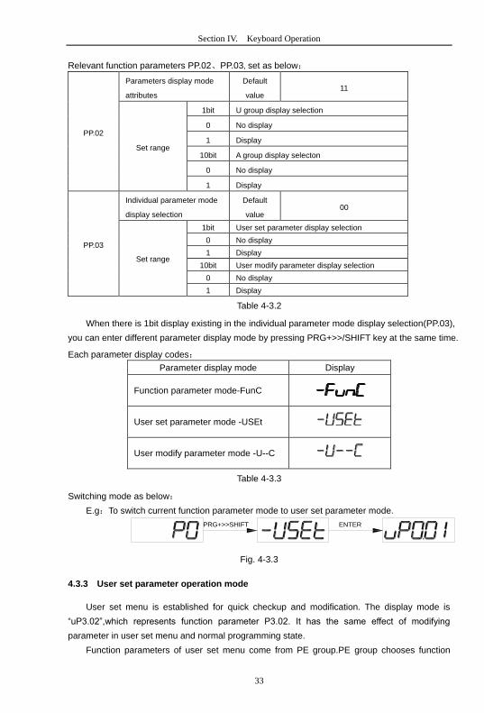
Relevant function parameters PP.02、PP.03, set as below:
PP.02
Parameters display mode
attributes
Default
value 11
Set range
1bit U group display selection
0 No display
1 Display
10bit A group display selecton
0 No display
1 Display
PP.03
Individual parameter mode
display selection
Default
value 00
Set range
1bit User set parameter display selection
0 No display
1 Display
10bit User modify parameter display selection
0 No display
1 Display
Table 4-3.2
When there is 1bit display existing in the individual parameter mode display selection(PP.03),
you can enter different parameter display mode by pressing PRG+>>/SHIFT key at the same time. Each parameter display codes:
Parameter display mode Display
Function parameter mode-FunC
User set parameter mode -USEt
User modify parameter mode -U--C
Table 4-3.3
Switching mode as below:
E.g:To switch current function parameter mode to user set parameter mode.
Fig. 4-3.3
4.3.3 User set parameter operation mode
User set menu is established for quick checkup and modification. The display mode is
“uP3.02”,which represents function parameter P3.02. It has the same effect of modifying
parameter in user set menu and normal programming state.
Function parameters of user set menu come from PE group.PE group chooses function
PRG+>>SHIFT ENTER

Section IV. Keyboard Operation
34
parameter:when PE is set to P0.00 ,it means no choosing,totally 30 functions can be set. If
display “NULL” when entering menu, it means user set menu is null.
16 parameters have been stored at initial time for user’s convenience:
P0.01:Control mode P0.02:Command source selection
P0.03:Main frequency source selection P0.07:Frequency source selection
P0.08:Preset frequency P0.17:Acceleration time
P0.18:Deceleration time P3.00:V/F curve set
P3.01:Torque boost P4.00:DI1Terminal function selection
P4.01:DI2terminal function selection P4.02:DI3 terminal function selection
P5.04:DO1output selection P5.07:AO1 output selection
P6.00:Startup mode P6.10:Stop mode
Users could modify the user set parameter according to specific need of your own.
4.3.4 Check method of state parameter
When the inverter is in stop or running status, multiple status parameters can be displayed.
It can select if this parameter is to be displayed in binary bit with the function codes P7.03
(running parameter1) , P7.04 (running parameter2) and P7.05(stop parameter).
In stop status, there are 4 running state parameter:set frequency, bus voltage,analog
input voltage AI1, analog input voltage AI2 which of them are of default display.Other display
parameters respectively:DI input state,DO output state,analog input voltage AI3, actual count
value, actual length value, PLC running steps, load speed display, PID set, PULSE input pulse
frequency and 3 reserved parameters (whether to display or not is determined by function code
P7.05 binary bit choice). Selected parameter are switched in sequence order.
In running status, there are a total of 5 running status parameters, including:setup
frequency, running frequency, bus voltage,output voltage,output current ,which of them are of
default display. Other display parameters respectively :output power, output torque, DI input
state,DO output state, analog input voltage AI1, analog input voltage AI2, analog input voltage
AI3, actual count value, actual length value, linear velocity, PID set, PID feedback etc. Whether
to display or not is determined by function code P7.03、P7.04 binary bit choice. Selected
parameter are switched in sequence order.
When inverter power on after powered off , the display parameter is the one that chosen
before power off as default.
4.3.5 Password Setting
The inverter provides user password protection function. When PP.00 is set to non-zero
value, it is user password and enabled after exiting the function code editing status. When the
user presses the PRG key again, “-----“will be displayed to require the user to enter user
password, or the user cannot enter the general menu.
To cancel the password protection function, the user needs to enter the relevant interface
through password, and change the PP.00 setting to 0.

Section IV. Keyboard Operation
35
4.3.6 Motor parameter automatic tuning
Vector control running mode:before running, user must accurately input motor nameplate
parameters. HV590 series inverter will be matching standard motor parameter according to this
nameplate. Vector control methods are very much dependent on motor parameters, to get good
control performance, accurate control motor parameters must be acquired.
Motor parameter auto tuning procedure is as follows:
Firstly, select command source(P0.02) as operation panel command channel.Secondly,
input parameters below in accordance with motor actual parameter:
Motor selection Parameter
Motor 1
P1.00:Motor type selection P1.01:Motor rated power
P1.02:Motor rated voltage P1.03:Motor rated current
P1.04:Motor rated frequency P1.05:Motor rated revolving speed
Motor 2
A2.00:Motor type selection A2.01:Motor rated power
A2.02:Motor rated voltage A2.03:Motor rated current
A2.04:Motor rated frequency A2.05:Motor rated revolving speed
Motor 3
A3.00:Motor type selection A3.01:Motor rated power
A3.02:Motor rated voltage A3.03:Motor rated current
A3.04:Motor rated frequency A3.05:Motor rated revolving speed
Motor 4
A4.00:Motor type selection A4.01:Motor rated power
A4.02:Motor rated voltage A4.03:Motor rated current
A4.04:Motor rated frequency A4.05:Motor rated revolving speed
Table 4-3.4
E.g:Asynchronous motor parameter tuning
If motor and the load can be totally separated, please select P1.37(Motor 2\3\4 as
A2\A3\A4.37) to 2(Asynchronous machine complete tuning), then press RUN key on keyboard
panel, inverter will automatically calculate the motor of the following parameters:
Motor selection Parameter
Motor 1
P1.06:Asynchronous motor stator resistance
P1.07: Asynchronous motor rotor resistance
P1.08: Asynchronous motor leakage inductance
P1.09: Asynchronous motor mutual inductance
P1.10: Asynchronous motor no-load current
Motor 2
A2.06: Asynchronous motor stator resistance
A2.07: Asynchronous motor rotor resistance

Section IV. Keyboard Operation
36
A2.08: Asynchronous motor leakage inductance
A2.09: Asynchronous motor mutual inductance
P2.10: Asynchronous motor no-load current
Motor 3
A3.06: Asynchronous motor stator resistance
A3.07: Asynchronous motor rotor resistance
A3.08: Asynchronous motor leakage inductance
A3.09: Asynchronous motor mutual inductance
P3.10: Asynchronous motor no-load current
Motor 4
A4.06: Asynchronous motor stator resistance
A4.07: Asynchronous motor rotor resistance
A4.08: Asynchronous motor leakage inductance
A4.09: Asynchronous motor mutual inductance
P4.10: Asynchronous motor no-load current
Table4-3.5
If motor and the load can not be totally separated, please select P1.37(Motor 2\3\4 as
A2\A3\A4.37) to 1(Asynchronous machine static tuning), then press RUN key on keyboard panel.
4.4 Test running
HV590 General machine type factory setting value
Code Factory setting Description
P0.01 0 Speed sensorless vector control(SVC)
P0.02 0 Operation panel command channel(LED OFF)
P0.03 4 AI3(Potentiometer)
Users set motor parameters P1.00~P1.05 to correct values, after parameters auto tuning,
motor operation can be directly controlled through keyboard, while frequency can be set through
keyboard potentiometer.
37
Section V. Parameter Function Table
Caution:
The symbols in the function table are explained as follows:
“”:indicates that the parameter setup value cannot be modified when the inverter is in the
running status.
“”:indicates that the parameter value is the actual detection record and cannot be modified.
“”:indicates that the parameter setup value can be modified when the inverter is in stop
status and running status.
“”:indicates that the parameter is “Factory default parameter” and can be set only by the
manufacturer, and the user is forbidden to perform any operation.
“-”:indicates that the parameter factory value is relevant to power or model, for specifications
please refer to corresponding parameter description.
“Change limit” indicates if the parameter is adjustable during operation.
When PP.0 is set to non-zero value, it means that the parameter protection password is set
and only when correct password is input can the user enter the parameter menu. To cancel the
password, PP.00should be set to 0.
In the user set parameter mode , parameter menu is not protected by password protection.
P group, A group are of basic function parameters, U group is the monitor function group.
5.1 Monitor function group:U0.00-U0.61
U0 parameter group is used to monitor inverter running status .Customers can check through
panel for field commissioning as well as read parameter value through communication for position
machine monitoring. Among which, U0.00~U0.31 is defined for running or stop monitor parameter
by P7.03 and P7.04.
For specific parameter function code、parameter name and minimum unit, please refer to the
table below.
Function code Designation Unit
U0.00 Running frequency(Hz) 0.01Hz
Inverter current actual setting frequency
U0.01 Setting frequency(Hz) 0.01Hz
Inverter current actual output frequency
U0.02 DC bus voltage(V) 0.1V
Detection value of DC bus voltage
U0.03 The output voltage(V) 1V
Inverteractual output voltage
U0.04 Motor output current(A) 0.01A
Valid value of motor actual current

38
Section V. Parameter Function Table
U0.05 The output power(kW) 0.1kW
The calculated value of actual output power of motor
U0.06 Output torque(%) 0.1%
The output torque of the motor
U0.07 DI input status 1
IO input status,it’s value is a hexadecimal digit.Each bit corresponds to each input terminal state:
0~14 bit Input status
0 Invalid
1 Valid
U0.08 Y output status 1
IO output status,it’s value is a hexadecimal digit.Each bit corresponds to each output terminal state :
0~9 bit Output status
0 Invalid
1 Valid
U0.09 AI1 voltage(V) 0.01V
AI1 input voltage, corrected by AC.00~AC.03
U0.10 AI2 voltage(V) 0.01V
AI2 input voltage, corrected by AC.04~AC.07
7 6 5 4 3 2 1 0
DI1
DI2
10 9 8
DI3
DI4
DI5
DI6
VDI5
VDI4
VDI3
VDI2
VDI1
2 2 2 2 2 2 2 201234567
2 2 28910
1114 13 12
211
2 2 2121314
DI7
DI8
DI10
DI9
7 6 5 4 3 2 1 0
Y1R
TA1-TB1-TC1
9 8
TA2-TB2-TC2
DO1
DO2 VDO1
VDO2
VDO3
VDO5
VDO4
2 2 2 2 2 2 2 2 0 1 2 3 4 5 6 7 2 2 8 9
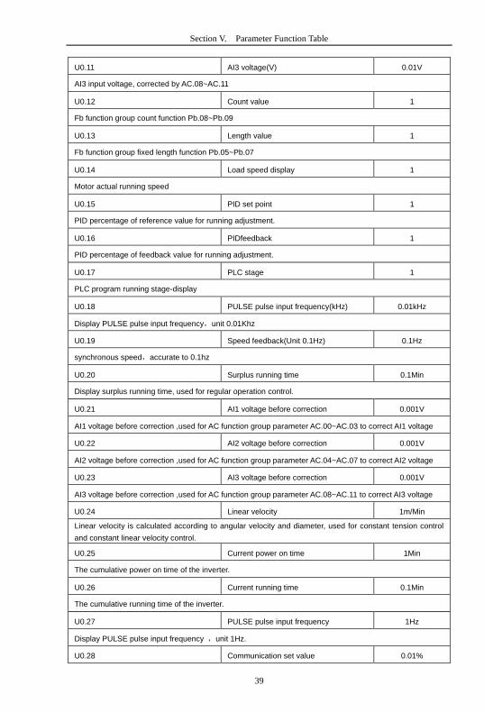
39
Section V. Parameter Function Table
U0.11 AI3 voltage(V) 0.01V
AI3 input voltage, corrected by AC.08~AC.11
U0.12 Count value 1
Fb function group count function Pb.08~Pb.09
U0.13 Length value 1
Fb function group fixed length function Pb.05~Pb.07
U0.14 Load speed display 1
Motor actual running speed
U0.15 PID set point 1
PID percentage of reference value for running adjustment.
U0.16 PIDfeedback 1
PID percentage of feedback value for running adjustment.
U0.17 PLC stage 1
PLC program running stage-display
U0.18 PULSE pulse input frequency(kHz) 0.01kHz
Display PULSE pulse input frequency,unit 0.01Khz
U0.19 Speed feedback(Unit 0.1Hz) 0.1Hz
synchronous speed,accurate to 0.1hz
U0.20 Surplus running time 0.1Min
Display surplus running time, used for regular operation control.
U0.21 AI1 voltage before correction 0.001V
AI1 voltage before correction ,used for AC function group parameter AC.00~AC.03 to correct AI1 voltage
U0.22 AI2 voltage before correction 0.001V
AI2 voltage before correction ,used for AC function group parameter AC.04~AC.07 to correct AI2 voltage
U0.23 AI3 voltage before correction 0.001V
AI3 voltage before correction ,used for AC function group parameter AC.08~AC.11 to correct AI3 voltage
U0.24 Linear velocity 1m/Min
Linear velocity is calculated according to angular velocity and diameter, used for constant tension control
and constant linear velocity control.
U0.25 Current power on time 1Min
The cumulative power on time of the inverter.
U0.26 Current running time 0.1Min
The cumulative running time of the inverter.
U0.27 PULSE pulse input frequency 1Hz
Display PULSE pulse input frequency ,unit 1Hz.
U0.28 Communication set value 0.01%

40
Section V. Parameter Function Table
Communication set value
U0.29 Encoder feedback speed 0.01Hz
PG feedback speed, accurate to 0.1hz
U0.30 Main frequency X display 0.01Hz
P0.03 main frequency source set frequency
U0.31 Auxiliary frequency Y display 0.01Hz
P0.04 auxiliary frequency source set frequency
U0.32 View arbitrary memory address value 1
To view arbitrary memory address, advanced commissioning function.
U0.33 Reserve 0.0°
U0.34 Motor temperature 1
Display motor temperature. Other device temperature can also be tested through different temperature
measuring point.
U0.35 Target torque(%) 0.1%
Target torque setup.In torque control mode, it is used to check the set target torque.
U0.36 Rotary variable position 1
It’s rotor position when speed feedback.
U0.37 Power factor angle 0.1
Current power factor angle,power factor=COS(angle),angle=0,maximum power.
U0.38 ABZ position 0.0
ABZ incremental feedback position information of encoder calculation.
U0.39 VF target voltage separation 1V
VF target voltage when power supply separating.
U0.40 VF output voltage separation 1V
VF output voltage when power supply separating.
U0.41 DI input status intuitive display -
Display DI input status intuitively, offer DI input information more detailed than U0.07, advanced
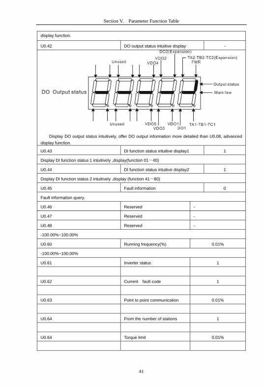
41
Section V. Parameter Function Table
display function.
U0.42 DO output status intuitive display -
Display DO output status intuitively, offer DO output information more detailed than U0.08, advanced
display function.
U0.43 DI function status intuitive display1 1
Display DI function status 1 intuitively ,display(function 01-40)
U0.44 DI function status intuitive display2 1
Display DI function status 2 intuitively ,display (function 41-80)
U0.45 Fault information 0
Fault information query.
U0.46 Reserved -
U0.47 Reserved -
U0.48 Reserved -
-100.00%~100.00%
U0.60 Running frequency(%) 0.01%
-100.00%~100.00%
U0.61 Inverter status 1
U0.62 Current fault code 1
U0.63 Point to point communication 0.01%
U0.64 From the number of stations 1
U0.64 Torque limit 0.01%
42
Section V. Parameter Function Table
5.2 Basic function group:P0.00-P0.28
Code Description/Display Setting Range Factory
Setting
Change
Limit
P0.00 GP type display G type(constant torque load type) 1
- P type(draught fan,pump load type) 2
This parameter is only for the use of viewing the factory model. It is can not be modified.
1:It is applicable to the constant torque load of specified rated parameter
2:It is applicable to the variable torque load of specified rated parameter(draught fan,pump load type)
P0.01 Motor 1 control mode
Speed sensorless vector control(SVC) 0
0 Speed sensor vector control(FVC) 1
V/F control 2
0:Speed sensorless vector control
It refers to the open-loop vector control that is generally applied to high performance control field. One
inverter can only drive one motor. E.g:machine tool, centrifugal machine, fiber drawing machine, injection
molding machine’ load etc.
1:Speed sensor vector control
It refers to the closed-loop vector control and encoder must be added to the motor end.Inverter must
be matching with the same type PG card of the encoder. This control mode is suitable for high precision
speed control and torque control field. One inverter can only drive one motor. E.g :high speed
papermaking machinery , hoisting machinery , elevator’load etc.
2:V/F control
V/F control mode is suitable for fields that load demand is not high or one inverter can drive multiple
motos. E.g:draught fan, pump’ load etc.
Tips:Motor parameters must be indentified before choosing vector control mode.Only accurate motor
parameters can play the advantage of vector control mode. Users can get better performance by adjusting
speed regulator group P2 parameters(motor 2,motor 3,motor 4 respectively for group A2,A3,A4)
FVC is generally used for permanent magnet synchronous motor, while part of the small power
applications can select V/F control mode. HV590 series support specific models of permanent magnet
synchronous motor sensorless vector control mode. Please refer to HV590 users manual and HV590S
dedicated users manual for using method.
P0.02 Command source selection
Operation panel command channel(LED
off) 0
0 Terminal command channel(LED on) 1
Serial port communicationcommand
channel(LED flashing) 2
Inverter control commands include: run, stop, forward rotation (FWD), reverse rotation (REV),
forward jog (FJOG), reverse jog (RJOG), etc.
0: Operation panel command channel (“LOCAL/REMOT” LED off);
Perform running command control with RUN, MF.K and STOP/RESET keyson the operation panel.
1: Terminal command channel (“LOCAL/REMOT” LED on);
Perform running command control with multifunctional input terminals such as FWD, REV, FJOG,
RJOG, and so on.
2:Serial port communication command channel (“LOCAL/REMOT” LED flashing).
The running command is given by the host computer via the communication mode. When the item is
choosen,it must be equipped with communication card(Modbus RTU 、 ProfibusDP card 、 users
programmable control card or CANopen card and so on).
For the communication protocol, please refer to “PD group communication parameters”and
43
Section V. Parameter Function Table
supplementary explanation of corresponding communication card for details.
Supplementary explanation for communication card is allotted with communication card.This manual
contains a brief description of communication card.
P0.03 Main frequency source X
selection
Digital setup(Preset frequency P0.08,
UP/DOWN can be modified, power off
without memory)
0
4
Digital setup(Preset frequency P0.08,
UP/DOWN can be modified, power off
with memory)
1
AI1 2
AI2 3
AI3(Potentiometer) 4
Pulse setup(DI5) 5
MS command 6
Simple PLC 7
PIDsetup 8
Communicaton setup 9
This parameter is used to select the main reference frequency input channel. Totally 10 main reference
frequency channels:
0:Digital setup(power off without memory)
Initial value of set frequency equals to P0.08 “preset frequency”.User can change inverter set
frequency value through keyboard ∧ key and ∨ key ( or multi-function input terminal UP,DOWN).
Inverter power on after powered off, frequency set value restored to P0.08 “Preset frequency”.
1:Digital setup(power off with memory)
Initial value of set frequency equals to P0.08 “preset frequency”. User can change inverter set
frequency value through keyboard ∧ key and ∨ key ( or multi-function input terminal UP,DOWN).
Inverter power on after powered off, frequency set value restored to the value that equals to setupof
last power off time. Correction is memorized through keyboard ∧ key and ∨ key or terminal UP,DOWN.
What needs to be reminded is, P0.23 is “Digital setup frequency memory selection”. P0.23 is used to
select correction whether to be memorized or cleared and is relevant to stop, irrelevant to power off
memory, please pay attention during operation.
2:AI1
3:AI2
4:AI3(Potentiometer)
Frequency is determined by analog input terminal. HV590 series control board offers 2 analog input
terminal(AI1,AI2), optional device HNC5PC1 card can offer 1 isolated analog input terminal(AI3x).
AI1,AI2 can be chosen as 0V~10V voltage input as well as 0mA~20mA current input by the jumper
J3,J4 on control board.
AI1、AI2 input voltage value has a corresponding relationship with target frequency, users can choose
them at will. HV590 offers 5 groups of corresponding relation curve, which 3 of them are linear
relationship(2-point correspondence), 2 of them are 4-point correspondence(any curve among them). User
can set through P4 group or A6 function code.
Function code P4.33 is used to set AI1~AI22-channel analog input. Choose 1 curve among the 5
respectively. For specific correspondence please refer to P4、A6 groups.
5:Pulse setup(DI5)
Pulse setup is set through terminal pulse. Signal standard:voltage range 9V~30V, frequency range
0kHz~100kHz. Set pulse can be only input through multi-function input terminal DI5.
44
Section V. Parameter Function Table
Relationship between DI5 input pulse frequency and corresponding settings is set through P4.28~P4.31.
It is linear relationship(2-point correspondence). Pulse input 100.0% refers to the percentage of P0.10 .
6:MS command
MS command running mode is set through different combination mode of digital input DI terminal.
There are 4 MS command terminals with 16 status of HV590 series. PC group function codes correspond
to 16 “MS command”. “MS command” is percentage relativing to P0.10( maximum frequency).
When digital input terminal DI is used as MS command terminal, user should set through P4 group.For
specifications please refer to P4 group.
7:Simple PLC
When frequency source is set to 7, running frequency source can be switched to any frequency
command during 1~16.
User can set frequency command retention time and acceleration/deceleration time respectively.For
specifications please refer to PC group .
8:PID
Running frequency is the output of PID control process. Generally used for field process closed-loop
control.
When PID is choosen, user should set relevant parameters of PA group “PID function”.
9:Communicaton setup
Communication setup refers to main frequency source that setting through communication method of
position machine.
HV590 series support 4 kinds of communication mode:Modbus、Profibus.DP、CANopen 3 kinds of
communication can not be used at the same time.
Communication card should be installed during the use of communication.4 kinds of communication
card are optional.User can select to buy according to the needs, and set parameter P0.28 correctly.
P0.04 Auxiliary frequency source
Y selection
Digital setup(preset frequency P0.08,
UP/DOWN adjustable, power off without
memory)
0
0
Digital setup(preset frequency P0.08,
UP/DOWN adjustable, power off with
memory)
1
AI1 2
AI2 3
AI3(Potentiometer) 4
PULSE setup (Dl5) 5
MS command 6
Simple PLC 7
PIDsetup 8
Communication setup 9
When the auxiliary frequency source is used as independent frequency reference channel (i.e.
frequency source switching from X to Y), it is used in the same way as the relative specifications of P0.03.
When the auxiliary frequency source is used as overlap reference (i.e. frequency source selection
switching from X plus Y or X to X plus Y), it has special points as follows:
1. When the auxiliary frequency source is digital reference, the preset frequency (P0.08) is
nonsensical, and it needs to adjust the main reference frequency through the keys “∧”and “∨” of the
keyboard (or UP andDOWN of multifunctional input terminals).
2. When the auxiliary frequency source is analog input reference (AI1、AI2、AI3) or pulse input
reference, 100% of input setup is relative to the auxiliary frequency source range,and can be set through
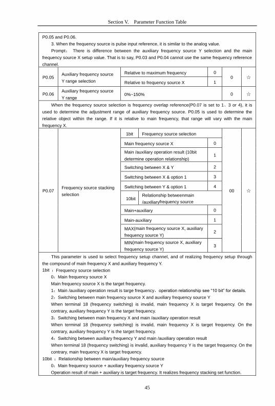
45
Section V. Parameter Function Table
P0.05 and P0.06.
3. When the frequency source is pulse input reference, it is similar to the analog value.
Prompt: There is difference between the auxiliary frequency source Y selection and the main
frequency source X setup value. That is to say, P0.03 and P0.04 cannot use the same frequency reference
channel.
P0.05 Auxiliary frequency source
Y range selection
Relative to maximum frequency 0 0
Relative to frequency source X 1
P0.06 Auxiliary frequency source
Y range 0%~150% 0
When the frequency source selection is frequency overlap reference(P0.07 is set to 1、3 or 4), it is
used to determine the adjustment range of auxiliary frequency source. P0.05 is used to determine the
relative object within the range. If it is relative to main frequency, that range will vary with the main
frequency X.
P0.07 Frequency source stacking
selection
1bit Frequency source selection
00
Main frequency source X 0
Main /auxiliary operation result (10bit
determine operation relationship) 1
Switching between X & Y 2
Switching between X & option 1 3
Switching between Y & option 1 4
10bit Relationship betweenmain
/auxiliaryfrequency source
Main+auxiliary 0
Main-auxiliary 1
MAX(main frequency source X, auxiliary
frequency source Y) 2
MIN(main frequency source X, auxiliary
frequency source Y) 3
This parameter is used to select frequency setup channel, and of realizing frequency setup through
the compound of main frequency X and auxiliary frequency Y.
1bit :Frequency source selection
0:Main frequency source X
Main frequency source X is the target frequency.
1:Main /auxiliary operation result is targe frequency,operation relationship see “10 bit” for details.
2:Switching between main frequency source X and auxiliary frequency source Y
When terminal 18 (frequency switching) is invalid, main frequency X is target frequency. On the
contrary, auxiliary frequency Y is the target frequency.
3:Switching between main frequency X and main /auxiliary operation result
When terminal 18 (frequency switching) is invalid, main frequency X is target frequency. On the
contrary, auxiliary frequency Y is the target frequency.
4:Switching between auxiliary frequency Y and main /auxiliary operation result
When terminal 18 (frequency switching) is invalid, auxiliary frequency Y is the target frequency. On the
contrary, main frequency X is target frequency.
10bit :Relationship between main/auxiliary frequency source
0:Main frequency source + auxiliary frequency source Y
Operation result of main + auxiliary is target frequency. It realizes frequency stacking set function.

46
Section V. Parameter Function Table
1:Main frequency source - auxiliary frequency source Y
Operation result of main - auxiliary is target frequency.
2:MAX(main frequency source X, auxiliary frequency source Y)
Choose bigger absolute value of the two as target frequency
3:MIN(main frequency source X, auxiliary frequency source Y)
Choose smaller absolute value of the two as target frequency.
Besides, when frequency source is main& auxiliary operation,users can set offset frequency through
P0.21.By stacking offset frequency on main& auxiliary operation result,it could flexible cope with all
kinds of needs.
P0.08 Preset frequency 0.00Hz to maximum frequency(It is only valid
when frequency source is set to “digital setting”) 50.00Hz
When set the frequency source to “digital setting” or “terminal UP/DOWN”, the parameter value is the
initial value of the inverter frequency digital setting.
P0.09 Running direction Consistent direction 0
0
Reverse direction 1
Modification of this parameter can change the rotary direction of the motor without changing any other
parameters, which is equivalent to the role of switching the rotary direction through adjusting any two lines
of the motor (U, V and W).
When needing to change the rotary direction of the motor, users can modify this parameter rather than
adjust the wiring of the motor.
Caution: When the function code is restored to the factory default value, this parameter value is
restored to 0, which should be used prudently in the applications where the motor rotary direction is not
allowed to change.
P0.10 Maximum frequency 50.00Hz~320.00Hz 50.00Hz
When analog input, pulse input(DI5), MS command etc are used as frequency source, their respective
100% are relatively calibrated through P0.10.
HV590 maximum frequency could reach 3200Hz. Users can set decimal digits of frequency command
through P0.22 to balance the idex of frequency command resolution and frequency input range.
When P0.22 is set to 1,frequency resolution ratio is 0.1Hz, P0.10 setting range is 50.0Hz~3200.0Hz;
When P0.22 is set to 2, frequency resolution ratio is 0.01Hz, P0.10 setting range is 50.00Hz~320.00Hz.
P0.11 Frequency source upper limit
P0.12 setup 0
0
AI1 1
AI2 2
AI3(Potentiometer) 3
PULSE setup 4
Communication setup 5
It defines the source of frequency upper limit. Frequency upper limit comes from digital setup (P0.12)
or analog input channel. When upper limt is set through analog input, 100% of analog input corresponds to
P0.12.
E.g : When winding control field is in the torque control mode, to avoid material break
phenomenon,users can set upper limit frequency through analog value. When running frequency reaches
value of upper limit , inverter maintains operation at the upper limit frequency.
P0.12 Frequency upper limit Frequency lower limit(P0.14) to maximum
frequency(P0.10) 50.00Hz
P0.13 Frequency upper limit offset 0.00Hz~maximum frequency P0.10 0.00Hz

47
Section V. Parameter Function Table
When upper limit is set through analog value or PULSE setup, P0.13 will be used as analog
valueoffset. The addition of offset frequency and analog setup value of frequency upper limit is used as
the final setup value of frequency upper limit.
P0.14 Frequency lower limit 0.00Hz to frequency upper limit P0.12 0.00Hz
When the running frequency of the inverter is lower than the frequency lower limit, it can select to
run at frequency lower limit or stop the inverter. Refer to P8.14 function code for details.
P0.15 Carrier frequency 0.5kHz~16.0kHz -
This function is used to adjust the carrier frequency of the inverter. By adjusting the carrier
frequency, the motor noise can be reduced, the resonance of the mechanical system can be avoided, so
that the leakage current to the ground and the interference of the inverter can be reduced.
When the carrier wave frequency is low, the output current higher harmonic component will be
increased, the motor loss will be increased, and the motor temperature rise will also be increased.
When the carrier wave frequency is high, the motor loss is reduced, and the motor temperature
rise is reduced, but the inverter loss and inverter temperature rise will be increased, and thus the
interference will be increased.
The adjustment of carrier frequency will influence the following items on the performance:
Carrier frequency low→ high
Motor noise big→ small
Output current waveform poor→ well
Motor temperature rise high→ low
Inverter temperature rise low→ high
Leakage current small→ large
Radiation interference small→ big
Different power of inverter is set with different carrier frequency by the factory. Though user could
modify it , attention should be paid:if carrier frequency is set higher than the factory set valule, it will
lead to inverter radiator temperature rise increasing. User should take inverter derating use, or there
will be danger of overheating alarm.
P0.16 Carrier frequency adjusting
with temperature
No 0 0
Yes 1
Carrier frequency adjusting with temperature refers to the detecting of radiator temperature. When
the temperature is high , carrier frequency automatically decreased to reduce the inverter temperature
rise. On the contrary , when the temperature is low, carrier frequency gradually restored to the set
value.This function could help to reduce the chance of inverter overheating alarm.
P0.17 Acceleration time 1 0.00s~65000s -
P0.18 Deceleration time 1 0.00s~65000s -
The acceleration time means the time t1 needed for the inverter to accelerate from 0Hz to the
reference frequency(P0.25).
The deceleration time means the time t2 needed for the inverter to decelerate from the reference
frequency (P0.25) to 0Hz.
The descriptionof acceleration and deceleration time are as shown in Fig.5.1:

48
Section V. Parameter Function Table
Fig.5-1Acceleration/decelerationtime schematic diagram
HV590 totally offers 4 groups of speed-up/speed-DOWN time for selection,you can shift through
digital input terminal DI,4 groups of them are shown as follows:
GROUP 1:P0.17、P0.18;
GROUP 2:P8.03、P8.04;
GROUP 3:P8.05、P8.06;
GROUP 4:P8.07、P8.08.
P0.19 Acc./dec. time unit
1second 0
1 0.1 seconds 1
0.01 seconds 2
HV590 offers 3 kinds of speed-up /speed down time unit to meet the need of all kinds of
scene.Respectively for 1 second、0.1 seconds and 0.01 seconds.
Caution:Decimal places as well as corresponding acceleration/deceleration time of the 4 groups may
be changed when modifying this function parameter,special attention should be paid in the process of
application.
P0.21 Auxiliary frequency source
offset frequency 0.00Hz~Maximum frequencyP0.10 0.00Hz
It is valid only at the time of main/auxiliary operation is choosen.
When frequency source is main / auxiliary operation(P0.21 as offset frequency) ,it could make
frequency set more flexible by stacking offset frequency on main& auxiliary operation as the final frequency
set value.
P0.22 Frequency command
resolution
0.1Hz 1 2
0.01Hz 2
This parameter is used to dertermine all the function code resolution which is relevant to frequency.
Frequency resolution is 0.1Hz , HV590 maximum output frequency can reach 3200Hz. While
frequency resolution is 0.01Hz, HV590 maximum output frequency is 320.00Hz.
Caution:Parameter (relating to frequency ) decimal digits and corresponding frequency value will
change through modifying P0.22. Special attention should be paid during operation.
P0.23 Digital setup frequency
memory selection upon stop
Without memory 0 0
Memory 1
This function is only valid when frequency source is digital setup.
0: Without memory
Actual deceleration time
Output frequency
Hz
t1 t2 Setting deceleration time
t
Acceleraion/deceleration
reference frequency
Setting frequency
Actual acceleration time
Setting acceleration time

49
Section V. Parameter Function Table
Upon power fault or stop of the inverter, set the frequency value back to the setup value of “Preset
Frequency” (P0.08). Frequency modification which set through keyboard “∧”、“∨” or terminal UP、
DOWN is cleared.
1: Memory
Digital setup frequency is the retention that reserved at last stop time. Keyboard “∧”、“∨” or
terminal UP、DOWN to make the correction valid.
P0.24 Motor selection
Motor 1 0
0 Motor 2 1
Motor 3 2
Motor 4 3
HV590 support applications that driving 4 motors in time-sharing. 4 motors can be set motor
nameplate parameters, independent parameter tuning, control mode, parameters relating to operation
performance respectively.
Motor 1 corresponding function groups are P1 group and P2 group. Motor 2,motor 3, motor 4
corresponding groups are A2 group, A3 group and A4 group respectively.
Users select current motor through P0.24 function code as well as digital input terminal DI. When
function code selecton conflicting with terminal DI selection, DI terminal selection is priority.
P0.25 Acceleration / deceleration
reference frequency
Maximum frequency(P0.10) 0
0 Set frequency 1
100Hz 2
Acceleration / deceleration time means the time needed for the inverter varying from 0Hz to the
frequency ofP0.25, Fig5.1 is acceleration / deceleration time schematic diagram.
When P0.25 is choosen to 1, acceleration / deceleration time is connected with set frequency.If set
frequency change frequently, the motor acceleration willchange,attention should be paid in applications.
P0.26 Frequency UP/DOWN
reference upon running
Running frequency 0 0
Set frequency 1
This parameter is only valid when frequency source is digital setting.
To select(through keyboard ∧、∨ key or terminal UP/DOWN) the modifying method of set
frequency, namely, target frequency is increasing/decreasing based on the running frequency or setting
frequency.
The difference between the two settings become apparently in inverter acceleration and
deceleration process.
P0.27 Command source &
frequency source binding
1bit Operation panel command bound
frequency source selection
000
Without binding 0
Digital setup frequency source 1
AI1 2
AI2 3
AI3(Potentiometer) 4
PULSE pulse setup(DI5) 5
MS command 6
Simple PLC 7
PID 8

50
Section V. Parameter Function Table
Communication setup 9
10bit Terminal command bound frequency
source selection
Without bound 0
Digital setup frequency source 1
AI1 2
AI2 3
AI3(Potentiometer) 4
PULSE pulse setup(DI5) 5
MS command 6
Simple PLC 7
PID 8
Communication setup 9
100bit Communication command binding
frequency source selection
Without bound 0
Digital setup frequency source 1
AI1 2
AI2 3
AI3(Potentiometer) 4
PULSE pulse setup(DI5) 5
MS command 6
Simple PLC 7
PID 8
Communication setup 9
It defines bound combination between 3 running command channels and 9 frequency setup
channels, which is easy to achieve synchronous switching.
Frequency setup channels above have the same definition with P0.03 “main frequency source X
selection”, please refer to P0.03 for details. Different running command channels can bind the same
frequency setup channel. When the command source is valid during command source & frequency
source binding, set frequency source of P0.03~P0.07 is invalid.
P0.28 Communication expansion
card
Modbus communication card 0
0 Profibus.DP communication card 1
CANopen communication card 2
CANlink communication card 3
HV590 series offers 3 kinds of communication mode. All of the 3 need to be equipped with optional
communication card .And they can not be used at the same time.
P0.28 is used to set the type of the optional communication card. When user replace the
communication card , P0.28 should be properly set.

51
Section V. Parameter Function Table
5.3 Parameters for motor 1:P1.00-P1.37
Code Description/Display Setting Range Factory
Setting
Change
Limit
P1.00 Motor type selection
General asynchronous motor 0
0 Variable frequency asynchronous motor 1
P1.01 Rated power 0.1kW~1000.0kW -
P1.02 Rated voltage 1V~2000V -
P1.03 Rated current 0.01A~655.35A(Inverter power≦55kW)
0.1A~6553.5A(Inverter power >55kW) -
P1.04 Rated frequency 0.01Hz~maximum frequency -
P1.05 Rated revolving speed 1rpm~65535rpm -
Function codes above are motor nameplate parameters. No matter VF control or vector control is the
choosen mode, users should accurately set the relating parameter according to the motor nameplate.
For better VF or vector control performance, users should tune the motor parameter. The accuracy of
the regulation results has intimate relationship with the accuracy of set motor nameplate parameters.
P1.06 Asynchronous motor stator
resistance
0.001Ω~65.535Ω(Inverter power <=55kW)
0.0001Ω~6.5535Ω(Inverter power >55kW) -
P1.07 Asynchronous motor rotor
resistance
0.001Ω~65.535Ω(Inverter power <=55kW)
0.0001Ω~6.5535Ω(Inverter power >55kW) -
P1.08 Asynchronous motor
leakage inductance
0.01mH~655.35mH(Inverter power <=55kW)
0.001mH~65.535mH(Inverter power >55kW) -
P1.09 Asynchronous motor mutual
inductance
0.1mH~6553.5mH(Inverter power <=55kW)
0.01mH~655.35mH(Inverter power >55kW) -
P1.10 Asynchronous motor no
load current
0.01A~P1.03(Inverter power <=55kW)
0.1A~P1.03(Inverter power >55kW) -
P1.06~P1.10 are parameters for asynchronous motor.Generally, motor nameplate dosen’t contain
such parameters, users can get them throung inverter auto tuning. Among them, 3 parameters
(P1.06~P1.08) can be get through “ asynchronous motor static tuning”, while all the 5 parameters as well
as encoder phase ,current loop PI etc can be get through“asynchronous motor complete tuning”. When
change the motor rated power (P1.01) or motor rated voltage (P1.02), inverter would automatically
modify the P1.06~P1.10 parameter value and restore them to common standard of Y series motor
parameter.
If the asynchronous motor is unable to be tuned, users could input above parameters with factory
offeredmotor value.
P1.27 Encoder pulses number 1~65535 2500
To set ABZ or UVW incremental encoder pulse number per revolution.
In the speed sensor vector control mode, P1.27 must be set accurately.Or motor would not normally
operate.
P1.28 Encoder type
ABZ incremental encoder 0
0 UVW incremental encoder 1
Rotary transformer 2
Sine/cosine encoder 3
52
Section V. Parameter Function Table
UVW encoder 4
HV590 support multiple encoder types. Different encoder should be equipped with different PG card.
For specifications please refer to Appendix IV. All the 5 encoders are suitable for synchronous motor,
while only ABZ incremental encoder and rotary transformer are suitable for asynchronous motor.
After installing the PG card, make sure that P1.28 is accurate according to actual situation.
P1.30 ABZ incremental encoder AB
phase
Forward 0 0
Reserve 1
This function code is only valid to ABZ incremental encoder(P1.28=0).It is used to set ABZ
incremental encoder AB signal phase sequence.
It is valid for both synchronous motor and asynchronous motor. Users could get ABZ encoder AB
phase sequence through asynchronous motor complete tuning or synchronous motor no-load tuning.
P1.31 Encoder installation angle 0.00~359.90 0.00
This parameter is only valid to synchronous motor control mode. It is valid for encoder types of ABZ
incremental encoder, UVW incremental encoder, rotary transformer,and UVW encoder.
P1.31 is available for synchronous motor complete / static tuning .It’s very important to operation of
synchronous motor. User should tune it before synchronous motor initial use.
P1.32 UVW phase sequence Forward 0
0
Reverse 1
P1.33 UVW encoder offset angle 0.00~359.90 0.00
P1.32 and P1.33 are only valid for synchronous motor using UVW encoder.
These two parameters can be obtained through synchronous motor complete / static tuning, which are
very important to operation of synchronous motor. Users should tune them before synchronous initial use.
P1.34 Rotary transformer pole pairs 1~65535 1
Rotary transformer is equipped with pole pairs.When using the encoder, correct parameters must be
set to it.
P1.36 PG dropped inspection time 0.0s:no action 0.1s~10.0s 0.0s
It is used to set inspection time of encoder disconnection fault.When feedback signal is 0.0s,
encoder disconnection fault will not be inspected.
If inverter detected disconnection fault,and the feedback value exceeded the P1.36 setup
range.Inverter fault alarm No. 20= E.PG1.
P1.37 Tuning selection
Without operation 0
0 Asynchronous static tuning 1 1
Asynchronous complete tuning 2
Asynchronous static tuning 2 3
Caution:Correct motor ratings must be set before tuning
0:No operation, tuning is forbidden.
1:Asynchronous motor static tuning 1
It is used for occasions that asynchronous motor and the load are not easily torn off, which may lead
to complete tuning invalid. Correct motor type and motor nameplate parameters P1.00~P1.05 must be
set before static tuning. User could get P1.06~P1.08 through tuing.
Action description:Set P1.37 to 1 and then press RUN button, inverter will carry out asynchronous
static tuning.
2:Asynchronous complete tuning
Asynchronous complete tuning can guarantee inverter dynamic control performance. Motor and the
load should be disconnected to keep motor complete status.
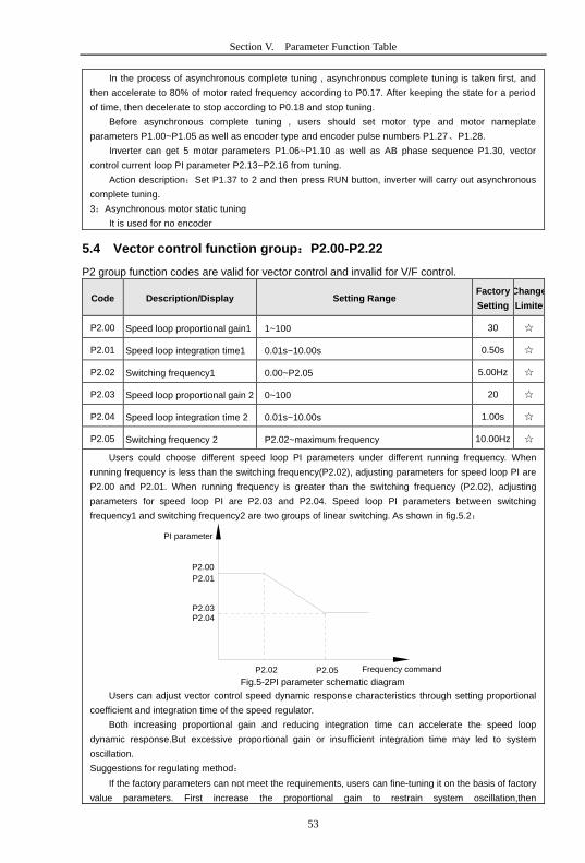
53
Section V. Parameter Function Table
In the process of asynchronous complete tuning , asynchronous complete tuning is taken first, and
then accelerate to 80% of motor rated frequency according to P0.17. After keeping the state for a period
of time, then decelerate to stop according to P0.18 and stop tuning.
Before asynchronous complete tuning , users should set motor type and motor nameplate
parameters P1.00~P1.05 as well as encoder type and encoder pulse numbers P1.27、P1.28.
Inverter can get 5 motor parameters P1.06~P1.10 as well as AB phase sequence P1.30, vector
control current loop PI parameter P2.13~P2.16 from tuning.
Action description:Set P1.37 to 2 and then press RUN button, inverter will carry out asynchronous
complete tuning.
3:Asynchronous motor static tuning
It is used for no encoder
5.4 Vector control function group:P2.00-P2.22
P2 group function codes are valid for vector control and invalid for V/F control.
Code Description/Display Setting Range Factory
Setting
Change
Limite
P2.00 Speed loop proportional gain1 1~100 30
P2.01 Speed loop integration time1 0.01s~10.00s 0.50s
P2.02 Switching frequency1 0.00~P2.05 5.00Hz
P2.03 Speed loop proportional gain 2 0~100 20
P2.04 Speed loop integration time 2 0.01s~10.00s 1.00s
P2.05 Switching frequency 2 P2.02~maximum frequency 10.00Hz
Users could choose different speed loop PI parameters under different running frequency. When
running frequency is less than the switching frequency(P2.02), adjusting parameters for speed loop PI are
P2.00 and P2.01. When running frequency is greater than the switching frequency (P2.02), adjusting
parameters for speed loop PI are P2.03 and P2.04. Speed loop PI parameters between switching
frequency1 and switching frequency2 are two groups of linear switching. As shown in fig.5.2:
Fig.5-2PI parameter schematic diagram
Users can adjust vector control speed dynamic response characteristics through setting proportional
coefficient and integration time of the speed regulator.
Both increasing proportional gain and reducing integration time can accelerate the speed loop
dynamic response.But excessive proportional gain or insufficient integration time may led to system
oscillation.
Suggestions for regulating method:
If the factory parameters can not meet the requirements, users can fine-tuning it on the basis of factory
value parameters. First increase the proportional gain to restrain system oscillation,then
P2.02 P2.05
P2.04P2.03
P2.01
P2.00
Frequency command
PI parameter
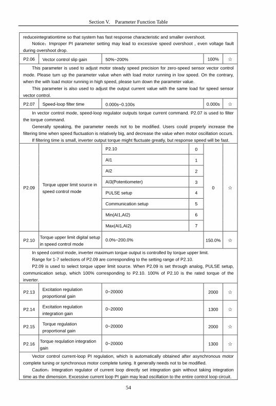
54
Section V. Parameter Function Table
reduceintegrationtime so that system has fast response characteristic and smaller overshoot.
Notice:Improper PI parameter setting may lead to excessive speed overshoot , even voltage fault
during overshoot drop.
P2.06 Vector control slip gain 50%~200% 100%
This parameter is used to adjust motor steady speed precision for zero-speed sensor vector control
mode. Please turn up the parameter value when with load motor running in low speed. On the contrary,
when the with load motor running in high speed, please turn down the parameter value.
This parameter is also used to adjust the output current value with the same load for speed sensor
vector control.
P2.07 Speed-loop filter time 0.000s~0.100s 0.000s
In vector control mode, speed-loop regulator outputs torque current command. P2.07 is used to filter
the torque command.
Generally speaking, the parameter needs not to be modified. Users could properly increase the
filtering time when speed fluctuation is relatively big, and decrease the value when motor oscillation occurs.
If filtering time is small, inverter output torque might fluctuate greatly, but response speed will be fast.
P2.09 Torque upper limit source in
speed control mode
P2.10 0
0
AI1 1
AI2 2
AI3(Potentiometer) 3
PULSE setup 4
Communication setup 5
Min(AI1,AI2) 6
Max(AI1,AI2) 7
P2.10 Torque upper limit digital setup
in speed control mode 0.0%~200.0% 150.0%
In speed control mode, inverter maximum torque output is controlled by torque upper limit.
Range for 1-7 selections of P2.09 are corresponding to the setting range of P2.10.
P2.09 is used to select torque upper limit source. When P2.09 is set through analog, PULSE setup,
communication setup, which 100% corresponding to P2.10. 100% of P2.10 is the rated torque of the
inverter.
P2.13 Excitation regulation
proportional gain 0~20000 2000
P2.14 Excitation regulation
integration gain 0~20000 1300
P2.15 Torque regulation
proportional gain 0~20000 2000
P2.16 Torque requlation integration
gain 0~20000 1300
Vector control current-loop PI regulation, which is automatically obtained after asynchronous motor
complete tuning or synchronous motor complete tuning. It generally needs not to be modified.
Caution:Integration regulator of current loop directly set integration gain without taking integration
time as the dimension. Excessive current loop PI gain may lead oscillation to the entire control loop circuit.
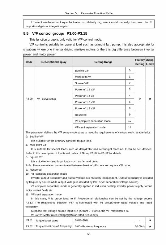
55
Section V. Parameter Function Table
If current oscillation or torque fluctuation is relatively big, users could manually turn down the PI
proportional gain or integration gain.
5.5 V/F control group:P3.00-P3.15
This function group is only valid for V/F control mode.
V/F control is suitable for general load such as draught fan, pump. It is also appropriate for
situations where one inverter driving multiple motors or there is big difference between inverter
power and motor power.
Code Description/Display Setting Range Factory
Setting
Change
Limite
P3.00 V/F curve setup
Beeline V/F 0
0
Multi-point V/F 1
Square V/F 2
Power of 1.2 V/F 3
Power of 1.4 V/F 4
Power of 1.6 V/F 6
Power of 1.8 V/F 8
Reserved 9
VF complete separation mode 10
VF semi separation mode 11
This parameter defines the V/F setup mode so as to meet the requirements of various load characteristics.
0:Beeline V/F
It is suitable for the ordinary constant torque load.
1:Multi-point V/F
It is suitable for special loads such as dehydrator and centrifugal machine. It can be self-defined.
Refer to the description of functional codes of Group F1-07 to F1-12 for details.
2:Square V/F
It is suitable for centrifugal loads such as fan and pump.
3~8:These are relation curve situated between beeline V/F curve and square V/F curve.
9:Reserved
10:VF complete separation mode
Inverter output frequency and output voltage are mutually independent. Output frequency is decided
by frequency source,while output voltage is decided by P3.13(VF separation voltage source).
VF complete separation mode is generally applied in induction heating, inverter power supply, torque
motor control fields etc.
11:VF semi separation mode
In this case, V is proportional to F. Proportional relationship can be set by the voltage source
P3.13. The relationship between V&F is connected with P1 group(motor rated voltage and rated
frequency).
Suppose that voltage source input is X (X from 0~100%), the V,F relationship is:
V/F=2*X*(Motor rated voltage)/(Motor rated frequency)
P3.01 Torque boost value 0.0%~30% -
P3.02 Torque boost cut-off frequency 0.00~Maximum frequency 50.00Hz

56
Section V. Parameter Function Table
Fig. 5-3 Manual torque boost schematic diagram
To compensate the low frequency torque characteristics of V/F control, boost compensation should be
made to inverter low frequency output voltage.
Torque hoist: it will be set according to the percentage of input rated voltage to the inverter. Below
are explanations of setting torque increase:
1) When the torque hoist is set as 0.0%, the inverter will aYpt auto torque hoist.
2) This parameter can be properly hoisted for small motor, while for large motor; the parameter can be
properly decreased.
3) If the torque hoist is set to be too large, the motor may be overheated, and the inverter may be
over-current.
Torque hoist cut-off frequency: As shown in Fig. 5.3, the torque hoist is valid when the cutoff
frequency below this setting. Otherwise, the torque hoist will be invalid.
P3.03 Multi-point V/F frequency
point F1 0.00Hz~P3.05 0.00Hz
P3.04 Multi-point V/F voltage point
V1 0.0%~100.0% 0.0%
P3.05 Multi-point V/F frequency
point F2 P3.03~P3.07 0.00Hz
P3.06 Multi-point V/F voltage point
V2 0.0%~100.0% 0.0%
P3.07 Multi-point V/F frequency
point F3
P3.05~Motor rated frequency(P1.04)Note:Motor
2\3\4 rated frequency respectively
A2.04\A3.04\A4.04
0.00Hz
P3.08 Multi-point V/F voltage point
V3 0.0%~100.0% 0.0%
Six parameters of P3.03 to P3.08 define the multi-point V/F curve.
The setup value of multi-point V/F curve is generally set in accordance with the load characteristics of
the motor.
Caution:
1) It must be set as follows: V1<V2<V3,F1<F2<F3. Fig5.4 is schematic diagram for multi-point
V/F curve.
2) If the voltage is set too high at the time of low frequency, it may cause overheating and even
burning of the motor as well as stall over current or over current protection of the inverter.
f1 Output frequencyfb
V1
Vb
Output voltage
V1:Manual torque boost voltage Vb:Maximum output voltage
f1:Cutt-off frequency of torque boost fb:Rated running frequency
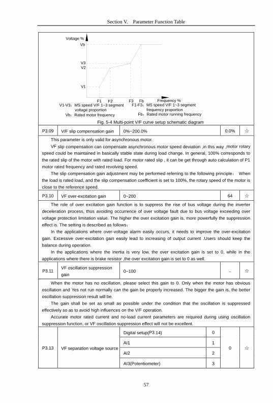
57
Section V. Parameter Function Table
Fig. 5-4 Multi-point V/F curve setup schematic diagram
P3.09 V/F slip compensation gain 0%~200.0% 0.0%
This parameter is only valid for asynchronous motor.
VF slip compensation can compensate asynchronous motor speed deviation ,in this way ,motor rotary
speed could be maintained in basically stable state during load change. In general, 100% corresponds to
the rated slip of the motor with rated load. For motor rated slip , it can be get through auto calculation of P1
motor rated frequency and rated revolving speed.
The slip compensation gain adjustment may be performed referring to the following principle: When
the load is rated load, and the slip compensation coefficient is set to 100%, the rotary speed of the motor is
close to the reference speed.
P3.10 VF over-excitation gain 0~200 64
The role of over excitation gain function is to suppress the rise of bus voltage during the inverter
deceleration process, thus avoiding occurrence of over voltage fault due to bus voltage exceeding over
voltage protection limitation value. The higher the over excitation gain is, more powerfully the suppression
effect is. The setting is described as follows:
In the applications where over-voltage alarm easily occurs, it needs to improve the over-excitation
gain. Excessive over-excitation gain easily lead to increasing of output current .Users should keep the
balance during operation.
In the applications where the inertia is very low, the over excitation gain is set to 0, while in the
applications where there is brake resistor ,the over excitation gain is set to 0 as well.
P3.11 VF oscillation suppression
gain 0~100 -
When the motor has no oscillation, please select this gain to 0. Only when the motor has obvious
oscillation and Yes not run normally can the gain be properly increased. The bigger the gain is, the better
oscillation suppression result will be.
The gain shall be set as small as possible under the condition that the oscillation is suppressed
effectively so as to avoid high influences on the V/F operation.
Accurate motor rated current and no-load current parameters are required during using oscillation
suppression function, or VF oscillation suppression effect will not be excellent.
P3.13 VF separation voltage source
Digital setup(P3.14) 0
0
AI1 1
AI2 2
AI3(Potentiometer) 3
F1 Frequency %
Voltage %
Vb
V3V2
V1
F2 F3 FbV1-V3:MS speed V/F 1~3 segment
voltage proportion
F1-F3:MS speed V/F 1~3 segment
frequency proportion
Vb:Rated motor frequency Fb:Rated motor running frequency
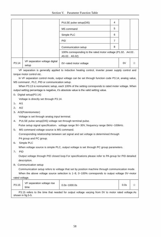
58
Section V. Parameter Function Table
PULSE pulse setup(DI5) 4
MS command 5
Simple PLC 6
PID 7
Communication setup 8
100% corresponding to the rated motor voltage (P1.02、A4.02、
A5.02、A5.02)
P3.14 VF separation voltage digital
setup 0V~rated motor voltage 0V
VF separation is generally applied to induction heating control, inverter power supply control and
torque motor control etc.
In VF separation control mode, output voltage can be set through function code P3.14, analog value,
MS command , PLC, PID or communication setup.
When P3.13 is nonnumeric setup, each 100% of the setting corresponds to rated moter voltage. When
output setting percentage is negative, it’s absolute value is the valid setting value.
0:Digital setup(P3.14)
Voltage is directly set through P3.14.
1: AI1
2: AI2
3:AI3(Potentiometer)
Voltage is set through analog input terminal.
4: PULSE pulse setup(DI5) voltage set through terminal pulse.
Pulse setup signal specification:voltage range 9V~30V, frequency range 0kHz~100kHz.
5: MS command voltage source is MS command.
Corresponding relationship between set signal and set voltage is determined through
P4 group and PC group.
6: Simple PLC
When voltage source is simple PLC, output voltage is set through PC group parameters.
7: PID
Output voltage through PID closed loop.For specifications please refer to PA group for PID detailed
description.
8:Communication setup
Communication setup refers to voltage that set by position machine through communication mode.
When the above voltage source selection is 1~8, 0~100% corresponds to output voltage 0V~motor
rated voltage.
P3.15 VF separation voltage rise
time 0.0s~1000.0s 0.0s
P3.15 refers to the time that needed for output voltage varying from 0V to motor rated voltage.As shown in fig.5-5.
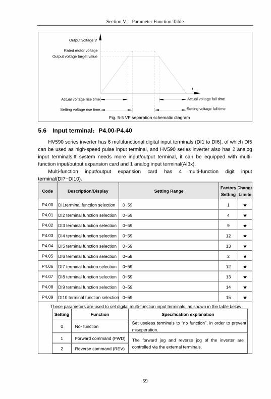
59
Section V. Parameter Function Table
Fig. 5-5 VF separation schematic diagram
5.6 Input terminal:P4.00-P4.40
HV590 series inverter has 6 multifunctional digital input terminals (DI1 to DI6), of which DI5
can be used as high-speed pulse input terminal, and HV590 series inverter also has 2 analog
input terminals.If system needs more input/output terminal, it can be equipped with multi-
function input/output expansion card and 1 analog input terminal(AI3x).
Multi-function input/output expansion card has 4 multi-function digit input
terminal(DI7~DI10).
Code Description/Display Setting Range Factory
Setting
Change
Limite
P4.00 DI1terminal function selection 0~59 1
P4.01 DI2 terminal function selection 0~59 4
P4.02 DI3 terminal function selection 0~59 9
P4.03 DI4 terminal function selection 0~59 12
P4.04 DI5 terminal function selection 0~59 13
P4.05 DI6 terminal function selection 0~59 2
P4.06 DI7 terminal function selection 0~59 12
P4.07 DI8 terminal function selection 0~59 13
P4.08 DI9 terminal function selection 0~59 14
P4.09 DI10 terminal function selection 0~59 15
These parameters are used to set digital multi-function input terminals, as shown in the table below:
Setting Function Specification explanation
0 No- function Set useless terminals to “no function”, in order to prevent
misoperation.
1 Forward command (FWD) The forward jog and reverse jog of the inverter are
controlled via the external terminals. 2 Reverse command (REV)
Actual voltage fall time
Output voltage V
Setting voltage fall time
t
Rated motor voltage
Output voltage target value
Actual voltage rise time
Setting voltage rise time
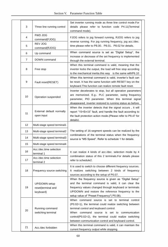
60
Section V. Parameter Function Table
3 Three line running control
Set inverter running mode as three line control mode.For
details please refer to function code P4.11(Terminal
command mode).
4 FWD JOG
command(FJOG) FJOG refers to jog forward running, RJOG refers to jog
reverse running. For jog running frequency, jog acc./dec.
time please refer to P8.00、P8.01、P8.02 for details. 5 REV JOG
command(RJOG)
6 Up command When command source is set as “Digital Setup”, the
increase or decrease of the set frequency is implemented
through the external terminal. 7 DOWN command
8 Free stop
When this terminal command is valid, meaning that the
inverter locks the output, the load will free stop according
to the mechanical inertia.this way is the same withP6.10
9 Fault reset(RESET)
When this terminal command is valid, inverter’s fault can
be reset. It has the same function with RESET key on the
keyboard.This function can realize remote fault reset.
10 Operation suspended
Inverter decelerates to stop, but all operation parameters
are memorized. E.g:PLC parameter, swing frequency
parameter, PID parameter. When this terminal signal
disappeared, inverter restored to running status as before.
11 External default normally
open input
When the inverter detects that the signal occurs , it will
report “15=Err15” fault, and handle the fault according to
the fault protection action mode.(Please refer to P9.47 for
details).
12 Multi-stage speed terminal1
The setting of 16-segment speeds can be realized by the
combinations of the terminal status when the frequency
source is “MS Speed”. Refer to schedule 1 for details.
13 Multi-stage speed terminal2
14 Multi-stage speed terminal3
15 Multi-stage speed terminal4
16 Acc./dec.time selection
terminal 1 It can realize 4 kinds of acc./dec. selection mode by 4
combination status of this 2 terminals.For details please
refer to schedule2. 17 Acc./dec.time selection
terminal 2
18 Frequency source switching
It is used to switch to choose different frequency sources.
It realizes switching between 2 kinds of frequency
sources according to the setup of P0.07.
19
UP/DOWN setup
reset(terminal and
keyboard)
When the frequency source is given as “Digital Setup”
and the terminal command is valid, it can clear the
frequency values changed through keyboard or terminals
UP/DOWN and restore the reference frequency to the
setup value of “Preset Frequency"( P0.08).
20 Running command
switching terminal
When command source is set to terminal control
(P0.02=1), the terminal could realize switching between
terminal control and keyboard control.
When command source is set to communication
control(P0.02=2), the terminal could realize switching
between communication control and keyboard control.
21 Acc./dec forbidden When this terminal command is valid, it can maintain the
current frequency output while stopping.

61
Section V. Parameter Function Table
22 PID pause
PID temporary invalid, the inverter maintains the current
frequency output and no longer taking PID adjustment of
frequency source.
23 PLC status reset
When this terminal command is valid, it clears the
memorized PLC running phase and running time, and
restores to the initial status of PLC running.
24 Swing frequency pause
When this terminal command is valid, the inverter maintains
the frequency output of the swing frequency center, and the
swing frequency pauses.
25 Counter input It is used as input terminal of the counting pulse.
26 Counter reset When this terminal command is valid, it clears the
counting value of the counter to zero.
27 Length counting input It is used as pulse input terminal of the length counting.
28 Length counting reset When this terminal is valid, it clears the length counting to
zero.
29 Torque control forbidden It prohibits inverter torque control. Inverter enters in
speed control mode.
30 PULSE frequency
input(Only valid for DI5) DI5 is used as pulse input terminal.
31 Reserved Reserved
32 Immediate DC braking When this terminal is valid, inverter directly switch to dc
braking state.
33 External default normally
closed input
When the inverter detects that the signal occurs , it will
report “Err15” fault, and stop running.
34 Frequency modification
enable
If the function is valid, inverter Yes not respond to
frequency change until the function turns to be invalid.
35 PID direction reversed PID and PA.03 set values are set in oppoisite directions
when the terminal is valid.
36 External stop terminal1 It could make inverter stop when in keyboard control.
Equivalent to function of STOP key on the keyboard.
37 Control command
switching terminal 2
It is used to switch control mode between terminal and
communication.
38 PID integration
suspension
When it is valid, PID integration regulation function pauses,
while PID proportional regulation and differential regulation
function are still valid.
39 Frequency source X and
preset frequency switching
When it is valid, frequency source X is replaced by the
preset frequency P0.08.
40 Frequency source Y and
preset frequency switching
When it is valid, frequency source Y is replaced by the
preset frequency P0.08.。
41 Motor selection terminal1 It can realize 4 groups of motor parameters switching by 4
combination status of this 2 terminals.For details please
refer to schedule3. 42 Motor selection terminal2
43 PID parameter switching
PA.18=1, the parameter is invalid, PID parameter takes
use of PA.05~PA.07. On the contrary, PA.15~PA.17 are
taken for the use.
44 User-defined fault 1 When user-defined fault 1&2 are valid, inverter alarm fault
number 27= E.USt1 & 28= E.USt2 respectively. Inverter will
handle the fault according to the mode selected by P9.49. 45 User-defined fault 2

62
Section V. Parameter Function Table
46 Speed control/ torque
control switching
It enables control mode to switch between inverter torque
control and speed control. Inverter running in the A0.00
defined mode when the terminal is invalid, and will switch
to another mode when it is valid.
47 Emergency stop
Inverter stops at the fastest speed when the terminal is
valid. Current is set to the current upper limit during this
stop process. This function is used for inverter fast stop ,
which can meet the stop need in system emergency.
48 External stop terminal 2
This terminal can be used to stopthe inverter in any
circumstances (panel control ,terminal control and
communication control). Deceleration time is fixed to
deceleration time 4.
49 Deceleration DC braking If it is valid, inverter first decelerates to stop DC braking
start frequency and then switches to DC braking state.
50 Running time reset Inverter running time of this time is cleared if the terminal is
valid. It operates with the use of P8.42 and P8.53.
51-59 Reserved Reserved
Schedule 1 MS command function description
4 MS command terminals, which can be combined into 16 states. For 16 corresponding values, please
refer to schedule 1 as below:
K4 K3 K2 K1 Command setup Corresponding
parameter
OFF OFF OFF OFF MS command 0 PC.00
OFF OFF OFF ON MS command 1 PC.01
OFF OFF ON OFF MS command 2 PC.02
OFF OFF ON ON MS command 3 PC.03
OFF ON OFF OFF MS command 4 PC.04
OFF ON OFF ON MS command 5 PC.05
OFF ON ON OFF MS command 6 PC.06
OFF ON ON ON MS command 7 PC.07
ON OFF OFF OFF MS command 8 PC.08
ON OFF OFF ON MS command 9 PC.09
ON OFF ON OFF MS command 10 PC.10
ON OFF ON ON MS command 11 PC.11
ON ON OFF OFF MS command 12 PC.12
ON ON OFF ON MS command 13 PC.13
ON ON ON OFF MS command 14 PC.14
ON ON ON ON MS command 15 PC.15
When frequency source is set to multi-stage speed mode, 100.0% of function code PC.00~PC.15 are
corresponding to maximum frequency P0.10. To meet the need, MS command can be used not only for
multi-stage speed function, but also PID setup source or VF separation voltage source.
Schedule 2 Acceleration / deceleration terminal selection description:
Terminal2 Terminal1 Acc./dec. selection Corresponding
parameter
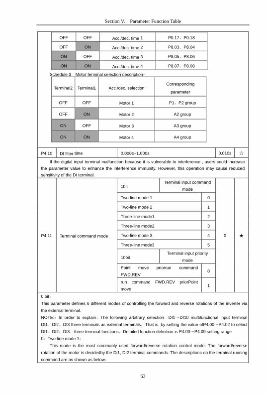
63
Section V. Parameter Function Table
OFF OFF Acc./dec. time 1 P0.17、P0.18
OFF ON Acc./dec. time 2 P8.03、P8.04
ON OFF Acc./dec. time 3 P8.05、P8.06
ON ON Acc./dec. time 4 P8.07、P8.08
Schedule 3 Motor terminal selection description:
Terminal2 Terminal1 Acc./dec. selection Corresponding
parameter
OFF OFF Motor 1 P1、P2 group
OFF ON Motor 2 A2 group
ON OFF Motor 3 A3 group
ON ON Motor 4 A4 group
P4.10 DI filter time 0.000s~1.000s 0.010s
If the digital input terminal malfunction because it is vulnerable to interference , users could increase
the parameter value to enhance the interference immunity. However, this operation may cause reduced
sensitivity of the DI terminal.
P4.11 Terminal command mode
1bit Terminal input command
mode
0
Two-line mode 1 0
Two-line mode 2 1
Three-line mode1 2
Three-line mode2 3
Two-line mode 3 4
Three-line mode3 5
10bit Terminal input priority
mode
Point move priorrun command
FWD,REV 0
run command FWD,REV priorPoint
move 1
0 bit:
This parameter defines 6 different modes of controlling the forward and reverse rotations of the inverter via
the external terminal.
NOTE::In order to explain,The following arbitrary selection DI1~DI10 multifunctional input terminal
DI1、DI2、DI3 three terminals as external terminals,That is, by setting the value ofP4.00~P4.02 to select
DI1、DI2、DI3 three terminal functions。Detailed function definition is P4.00~P4.09 setting range
0:Two-line mode 1:
This mode is the most commanly used forward/reverse rotation control mode. The forward/reverse
rotation of the motor is decidedby the Di1, DI2 terminal commands. The descriptions on the terminal running
command are as shown as below:
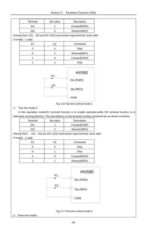
64
Section V. Parameter Function Table
Terminal Set value Description
DI1 1 Forward(FWD)
DI2 2 Reverse(REV)
Among them ,DI1、DI2 are DI1~DI10 muti-fuction input terminal, level valid.
0 invalid,1 valid
K1 K2 Command
0 0 Stop
0 1 Reverse(REV)
1 0 Forward(FWD)
1 1 Stop
Fig. 5-6 Two-line control mode 1
1: Two-line mode 2:
In this operation mode,DI1 terminal function is to enable operation,while DI2 terminal function is to
determine running direction. The descriptions on the terminal running command are as shown as below:
Terminal Set value Description
DI1 1 Forward(FWD)
DI2 2 Reverse(REV)
Among them ,DI1、DI2 are DI1~DI10 multi-fuction input terminal, level valid
0 invalid,1 valid
K1 K2 Command
0 0 Stop
0 1 Stop
1 0 Forward(FWD)
1 1 Reverse(REV)
Fig. 5-7 Two-line control mode 2
2:Three-line mode1
K2
K1
DIx (FWD)
DIy (REV)
COM
HV590
K2
K1
DIx (FWD)
DIy (REV)
COM
HV590
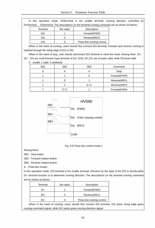
65
Section V. Parameter Function Table
In this operation mode, DI3terminal is the enable terminal, running direction controlled by
DI1terminal 、DI2terminal. The descriptions on the terminal running command are as shown as below:
Terminal Set value Description
DI1 1 Forward(FWD)
DI2 2 Reverse(REV)
DI3 3 Three-line running control
When in the need of running, users should first connect DI3 terminal. Forward and reverse running is
realized through the rising edge of Di1 or DI2.
When in the need of stop, user should disconnect DI3 terminal to meet the need. Among them, DI1、
DI2、DI3 are multi-function input terminal of DI1~DI10. DI1,DI2 are of pulse valid, while DI3 level valid.
0 invalid. 1 valid. X arbitrarily
SB1 SB2 SB3 Command
0 X X Stop
1 1 0 Forward(FWD)
1 0 1 Reverse(REV)
1 1 0->1 Reverse(REV)
1 0->1 1 Forward(FWD)
Fig. 5-8 Three-line control mode 1
Among them:
SB1:Stop button
SB2:Forward rotation button
SB3:Reverse rotation button
3:Three-line mode2
In this operation mode, DI3 terminal is the enable terminal, Direction by the state of the DI2 to decide,while
DI1 terminal function is to determine running direction. The descriptions on the terminal running command
are as shown as below:
Terminal Set value Description
DI1 1 Forward(FWD)
DI2 2 Reverse(REV)
DI3 3 Three-line running control
When in the need of running, users should first connect DI3 terminal. DI1 pulse rising edge gives
running command signal, while DI2 status gives running direction signal.
HV590
DIy (REV)
COM
DIx (FWD)
DIn 3-line running control
SB2
SB1
SB3

66
Section V. Parameter Function Table
When in the need of stop, user should disconnect DIn terminal to meet the need. Among them, DI1, DI2,
DI3 are multi-function input terminals of DI1~DI10. DI1 is of pulse valid, while DI2, DI3is of level valid.
0 invalid. 1 valid. X arbitrarily
SB1 SB2 K Command
0 X X Stop
1 1 0 Forward(FWD)
1 1 1 Reverse(REV)
Fig. 5-9 Three-line control mode 2
Among them :
SB1:Stop button
SB2:Running button
4:Two-line mode3
this operation mode is Priority control two-line mode.The forward/reverse rotation of the motor is
decidedby the Di1, DI2 terminal commands. The descriptions on the terminal running command are as
shown as below:
Terminal Set value Description
DI1 1 Forward(FWD)
DI2 2 Reverse(REV)
Among them ,DI1、DI2 are DI1~DI10 multi-fuction input terminal, level valid
0 invalid,1valid
K1 K2 Command
0 0 Stop
0 1 Reverse(REV)
1 0 Forward(FWD)
1 0->1 Forward(FWD)
0->1 1 Reverse(REV)
5:Three-line mode3
In this operation mode, DI3 terminal is the enable terminal, running direction controlled by
DI1terminal 、DI2terminal. The descriptions on the terminal running command are as shown as below:
HV590
DIy (REV)
COM
DIx (FWD)
DIn 3-line running control
SB2
SB1
K

67
Section V. Parameter Function Table
Terminal Set value Description
DI1 1 Forward(FWD)
DI2 2 Reverse(REV)
DI3 3 Three-line running control
When in the need of running, users should first connect DI3 terminal. Forward and reverse running is
realized through the rising edge of Di1 or DI2
Direction as first control priority control,when DI1 is valid,DI2 pulse rising edge is invalid,when DI2 is
valid,DI1 pulse rising edge is invalid,When in the need of stop, user should disconnect DI3 terminal to
meet the need. Among them, DI1、DI2、DIn are multi-function input terminal of DI1~DI10. DI1,DI2 are of
pulse valid, while DI3 level valid.
0 invalid. 1 valid. X arbitrarily
SB1 SB2 SB3 Command
0 X X Stop
1 1 0 Forward(FWD)
1 0 1 Reverse(REV)
1 1 0->1 Forward(FWD)
1 0->1 1 Reverse(REV)
Fig. 5-8 Three-line control mode 1
Among them:
SB1:Stop button
SB2:Forward rotation button
SB3:Reverse rotation button
P4.12 Terminal UP/DOWN variation
rate 0.01Hz/s~65.535Hz/s 1.00Hz/s
It is used to set the frequency variation rate (frequency variation per second) when adjusting the set
frequency with terminals UP/DOWN.
When P0.22 (frequency decimal point) is set to 2, range of P4.12 value is 0.001Hz/s~65.535Hz/s.
When P0.22 (frequency decimal point) is set to 1, range of P4.12 value is 0.01Hz/s~655.35Hz/ s.
P4.13 AI curve 1 minimum input 0.00V~P4.15 0.00V
P4.14 AI curve 1 minimum input
corresponding setup -100.00%~100.0% 0.0%
P4.15 AI curve 1 maximum input P4.13~10.00V 10.00V
HV590
DIy (REV)
COM
DIx (FWD)
DIn 3-line running control
SB2
SB1
SB3

68
Section V. Parameter Function Table
P4.16 AI curve 1 maximum input
corresponding setup -100.00%~100.0% 100.0%
P4.17 AI1 filter time 0.00s~10.00s 0.10s
Fig. 5-10 Relationship between analog input and setup value
The parameters mentioned above define the relationship between analog input voltage and the analog
input setup value.
When analog input voltage exceeds the setup “maximum input” limit, analog voltage is calculated as
“maximum input” .Similarly, when analog input is smaller than the setup “minimum input”,analog voltage is
calculated as minimum input or 0.0% according to the setting of P4.34.
AI used as current input terminal :1mA current equals to 0.5V voltage.
AI input filtering time is used to set AI1 software filtering time.When field anlog quantity is vulnerable,
please increase the filtering time so that anlog quantity tends to be stable. But excessive filtering time will
lead to slow response time to anlog detection. User should balance it according to practical application
cases.
In various application cases, the nominal value corresponding to 100% of analog reference will be
different. Refer to specific application description for the specific value.
100%
Corresponding setting
(frequency,torque)
0V(0mA) 10V(20mA)
A1
100%
0V(0mA) 10V(20mA)
A1
-100%
Corresponding setting
(frequency,torque)
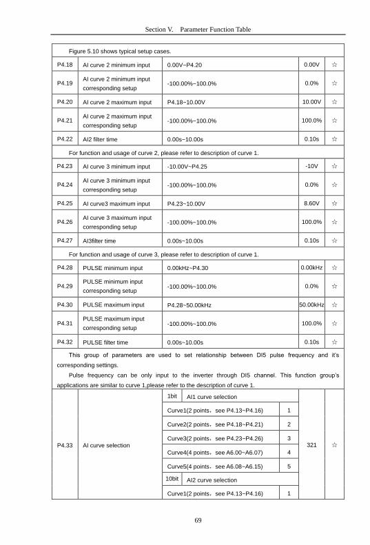
69
Section V. Parameter Function Table
Figure 5.10 shows typical setup cases.
P4.18 AI curve 2 minimum input 0.00V~P4.20 0.00V
P4.19 AI curve 2 minimum input
corresponding setup -100.00%~100.0% 0.0%
P4.20 AI curve 2 maximum input P4.18~10.00V 10.00V
P4.21 AI curve 2 maximum input
corresponding setup -100.00%~100.0% 100.0%
P4.22 AI2 filter time 0.00s~10.00s 0.10s
For function and usage of curve 2, please refer to description of curve 1.
P4.23 AI curve 3 minimum input -10.00V~P4.25 -10V
P4.24 AI curve 3 minimum input
corresponding setup -100.00%~100.0% 0.0%
P4.25 AI curve3 maximum input P4.23~10.00V 8.60V
P4.26 AI curve 3 maximum input
corresponding setup -100.00%~100.0% 100.0%
P4.27 AI3filter time 0.00s~10.00s 0.10s
For function and usage of curve 3, please refer to description of curve 1.
P4.28 PULSE minimum input 0.00kHz~P4.30 0.00kHz
P4.29 PULSE minimum input
corresponding setup -100.00%~100.0% 0.0%
P4.30 PULSE maximum input P4.28~50.00kHz 50.00kHz
P4.31 PULSE maximum input
corresponding setup -100.00%~100.0% 100.0%
P4.32 PULSE filter time 0.00s~10.00s 0.10s
This group of parameters are used to set relationship between DI5 pulse frequency and it’s
corresponding settings.
Pulse frequency can be only input to the inverter through DI5 channel. This function group’s
applications are similar to curve 1,please refer to the description of curve 1.
P4.33 AI curve selection
1bit AI1 curve selection
321
Curve1(2 points,see P4.13~P4.16) 1
Curve2(2 points,see P4.18~P4.21) 2
Curve3(2 points,see P4.23~P4.26) 3
Curve4(4 points,see A6.00~A6.07) 4
Curve5(4 points,see A6.08~A6.15) 5
10bit AI2 curve selection
Curve1(2 points,see P4.13~P4.16) 1

70
Section V. Parameter Function Table
Curve2(2 points,see P4.18~P4.21) 2
Curve3(2 points,see P4.23~P4.26) 3
Curve4(4 points,see A6.00~A6.07) 4
Curve5(4 points,see A6.00~A6.07) 5
100bit AI3 curve selection
Curve1(2 points,see P4.13~P4.16) 1
Curve2(2 points,see P4.18~P4.21) 2
Curve3(2 points,see P4.23~P4.26) 3
Curve4(4 points,see A6.00~A6.07) 4
Curve5(4 points,see A6.00~A6.07) 5
The 1bit, 10bit, 100bit of the function code are used to choose the set curve of analog input AI1、
AI2、AI3 respectively.
3 analog input can choose any curve of the 5 types.
Curve1, curve 2, curve 3 are 2 points curve that set through P4 group function codes, while curve 4,
curve 5 are 4 points curve that set through A8 group function codes.
HV590 standard unit offers 3-channel analog input terminals. Multi-function I/O expansion card is
needed in the use of AI3x.
P4.34 AI below minimum input
setup selection
1bit AI1 below minimum input setup
selection
000
Minimum input setup 0
0.0% 1
10bit AI2 below minimum input setup selection
Minimum input setup 0
0.0% 1
100bit AI3 below minimum input set selection
Minimum input setup 0
0.0% 1
This function code is used to dertermine analog quantity corresponding setup when analog input
voltage below the setup of minimum input.
The 1bit, 10bit, 100bit of the function code are corresponding to the analog input AI1、AI2、AI3
respectively. If the bit is set to 0 and AI is below the minimum setup , the analog input setup is the curve
“minimum input corresponding setup”(P4.14、P4.19、P4.24) . If the bit is set to 0 and AI is below the
minimum setup , the analog quantity corresponding setup is 0.0%.
P4.35 DI1 delay time 0.0s~3600.0s 0.0s
P4.36 DI2 delay time 0.0s~3600.0s 0.0s
P4.37 DI3 delay time 0.0s~3600.0s 0.0s
Only DI1, DI2, DI3 are able to set equipment delay time.
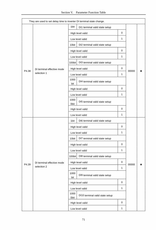
71
Section V. Parameter Function Table
They are used to set delay time to inverter DI terminal state change.
P4.38 DI terminal effective mode
selection 1
1bit DI1 terminal valid state setup
00000
High level valid 0
Low level valid 1
10bit DI2 terminal valid state setup
High level valid 0
Low level valid 1
100bit DI3 terminal valid state setup
High level valid 0
Low level valid 1
1000
bit DI4 terminal valid state setup
High level valid 0
Low level valid 1
1000
0bit DI5 terminal valid state setup
High level valid 0
Low level valid 1
P4.39 DI terminal effective mode
selection 2
1bit DI6 terminal valid state setup
00000
High level valid 0
Low level valid 1
10bit DI7 terminal valid state setup
High level valid 0
Low level valid 1
100bit DI8 terminal valid state setup
High level valid 0
Low level valid 1
1000
bit DI9 terminal valid state setup
High level valid 0
Low level valid 1
1000
0bit DI10 terminal valid state setup
High level valid 0
Low level valid 1

72
Section V. Parameter Function Table
It is used to set digital input terminal effective mode.
High level valid:Connection between COM and corresponding DI is valid,disconnection invalid.
Low level valid:Connection between COM and corresponding DI is invalid,disconnection valid.
5.7 Output terminal:P5.00-P5.22
HV590 series inverter provides two multifunctional analog terminal output selections,two
multifunctional relay output terminal, oneDO terminal (can be used as high speed pulse output
terminal as well as open collector switching output). If the above output terminals can not meet
the field application, users should choose optional multi-function input/output expansion card.
Output terminals of multi-fuction input/output expansion card contain 1 multi-function analog
output terminal(DO2), 1 multi-function relay output terminal (relay 2) , 1 multi-function digital
output terminal(DO2).
Code
Description/
Keyboard Display Setting Range
Factory
Setting
Change
Limite
P5.00 Y terminal output mode
selection
Pulse output(Y1P) 0
0
Switch output(Y1R) 1
Y1 is programmable multiplex terminal, which can be used as high speed pulse output terminal (Y1P)
or open collector switching output terminal (Y1R).
When P5.00 is set to 0, maximum output frequency can reach 10kHz , please refer to P5.06 for related
description.
P5.01 Y1Rselection (open
collector output terminal) 0-40 0
P5.02 Relay output selection
(TA1.TB1.TC1) 0-40 2
P5.03 Expansion card relay output
selection(TA2.TB2.TC2) 0-40 2
P5.04 DO1 output selection(open
collector output terminal) 0-40 1
P5.05 Expansion card DO2 output
selection 0-40 1
The above 5 function codes are used to select 5 digital output function. TA1.TB1.TC1 and
TA2.TB2.TC2 are control board and expansion card relay respectively.
Function selections are as follows:
Set
value Function Description
0 No output The output terminals have no function
1 Inverter in operation When the inverter is running, ON signal is output.
2 Output fault(Stop fault) When inverter fault happens and stops due to the fault ,
ON signal is output
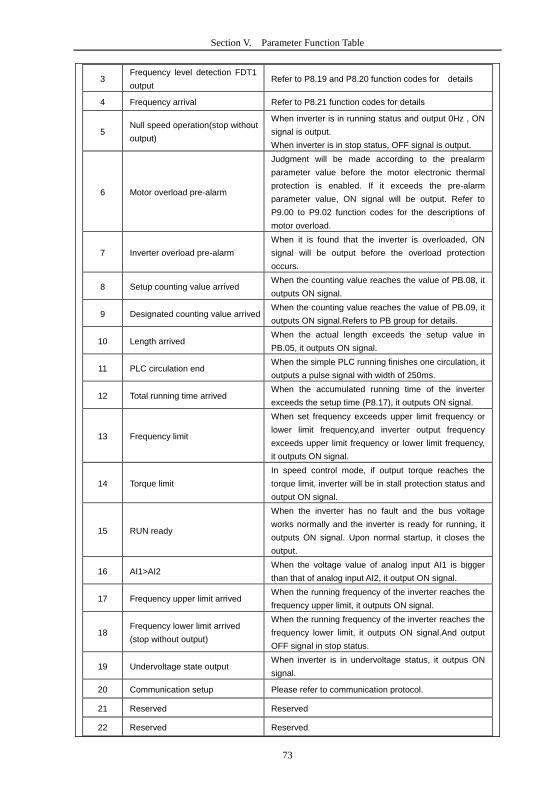
73
Section V. Parameter Function Table
3 Frequency level detection FDT1
output Refer to P8.19 and P8.20 function codes for details
4 Frequency arrival Refer to P8.21 function codes for details
5 Null speed operation(stop without
output)
When inverter is in running status and output 0Hz , ON
signal is output.
When inverter is in stop status, OFF signal is output.
6 Motor overload pre-alarm
Judgment will be made according to the prealarm
parameter value before the motor electronic thermal
protection is enabled. If it exceeds the pre-alarm
parameter value, ON signal will be output. Refer to
P9.00 to P9.02 function codes for the descriptions of
motor overload.
7 Inverter overload pre-alarm
When it is found that the inverter is overloaded, ON
signal will be output before the overload protection
occurs.
8 Setup counting value arrived When the counting value reaches the value of PB.08, it
outputs ON signal.
9 Designated counting value arrived When the counting value reaches the value of PB.09, it
outputs ON signal.Refers to PB group for details.
10 Length arrived When the actual length exceeds the setup value in
PB.05, it outputs ON signal.
11 PLC circulation end When the simple PLC running finishes one circulation, it
outputs a pulse signal with width of 250ms.
12 Total running time arrived When the accumulated running time of the inverter
exceeds the setup time (P8.17), it outputs ON signal.
13 Frequency limit
When set frequency exceeds upper limit frequency or
lower limit frequency,and inverter output frequency
exceeds upper limit frequency or lower limit frequency,
it outputs ON signal.
14 Torque limit
In speed control mode, if output torque reaches the
torque limit, inverter will be in stall protection status and
output ON signal.
15 RUN ready
When the inverter has no fault and the bus voltage
works normally and the inverter is ready for running, it
outputs ON signal. Upon normal startup, it closes the
output.
16 AI1>AI2 When the voltage value of analog input AI1 is bigger
than that of analog input AI2, it output ON signal.
17 Frequency upper limit arrived When the running frequency of the inverter reaches the
frequency upper limit, it outputs ON signal.
18 Frequency lower limit arrived
(stop without output)
When the running frequency of the inverter reaches the
frequency lower limit, it outputs ON signal.And output
OFF signal in stop status.
19 Undervoltage state output When inverter is in undervoltage status, it outpus ON
signal.
20 Communication setup Please refer to communication protocol.
21 Reserved Reserved
22 Reserved Reserved

74
Section V. Parameter Function Table
23 Null speed operation 2(Stop with
output)
When inverter output 0Hz , ON signal is output.
When inverter is in stop status, ON signal is output.
24 Total power-on time arrival When accumulated power-on time(P7.13) exceeds
P8.16 set value, it outputs ON signal.
25 Inspection level of FDT2 frequency Please refer to function code P8.28、P8.29 for details.
26 Frequency 1 arrival output Please refer to function code P8.30、P8.31 for details.
27 Frequency 2 arrival output Please refer to function code P8.32、P8.33 for details.
28 Current 1 arrival output Please refer to function code P8.38、P8.39 for details.
29 Current 2 arrival output Please refer to function code P8.40、P8.41 for details.
30 Timing arrival output When inverter running time reaches the set timming
(P8.42 valid), it outputs ON signal.
31 AI1excessive input
When analog input value AI1 is bigger than P8.46 (AI1
input protection upper limit) or smaller than P8.45(AI1
input protection lower limit), it outpus ON signal.
32 Load off Inverter in load off status, it outpus ON signal.
33 Reverse running Inverter in reverse running mode, it outputs ON signal.
34 Zero current state Please refer to function code P8.28、P8.29 for details.
35 Module temperature arrival When module radiator temperature(P7.07) reaches the
set value of P8.47, it outputs ON signal.
36 Software excessive current Please refer to function code P8.36、P8.37 for details.
37 Frequency lower limit arrival(stop
with output)
When running frequency reaches frequency lower limit,
it outputs ON signal.When in stop status ,it outputs ON
signal too.
38 Alarm output When inverter fault with processing mode of continue
running, it outputs alarm signal.
39 Motor over temperature alarm
When motor temperature reaches set value of P9.58 , it
outputs ON signal.(temperature can be viewed through
U0.34)
40 The running time arrival When the running time exceeds the set value of P8.53 ,
it outputs ON signal.
41 Alarm output
When inverter fault with processing mode of continue
running(uninclude under voltage fault), it outputs alarm
signal.
42 running command status output running command status direct output ( run
command)
43 Forward running command
status output
Forward running command status direct output
(forward run command)
44 Reverse running command
status output
Reverse running command status direct output
(Reverse run command)
P5.06
Y1P output function
selection(pulse output
terminal)
0-16 0
P5.07 AO1 output function selection 0-16 0
P5.08 AO2 output function selection 0-16 1
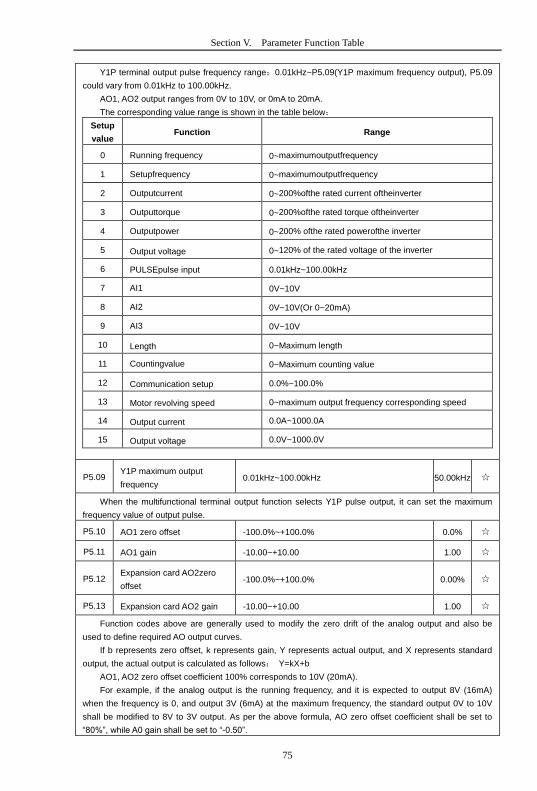
75
Section V. Parameter Function Table
Y1P terminal output pulse frequency range:0.01kHz~P5.09(Y1P maximum frequency output), P5.09
could vary from 0.01kHz to 100.00kHz.
AO1, AO2 output ranges from 0V to 10V, or 0mA to 20mA.
The corresponding value range is shown in the table below:
Setup
value Function Range
0 Running frequency 0~maximumoutputfrequency
1 Setupfrequency 0~maximumoutputfrequency
2 Outputcurrent 0~200%ofthe rated current oftheinverter
3 Outputtorque 0~200%ofthe rated torque oftheinverter
4 Outputpower 0~200% ofthe rated powerofthe inverter
5 Output voltage 0~120% of the rated voltage of the inverter
6 PULSEpulse input 0.01kHz~100.00kHz
7 AI1 0V~10V
8 AI2 0V~10V(Or 0~20mA)
9 AI3 0V~10V
10 Length 0~Maximum length
11 Countingvalue 0~Maximum counting value
12 Communication setup 0.0%~100.0%
13 Motor revolving speed 0~maximum output frequency corresponding speed
14 Output current 0.0A~1000.0A
15 Output voltage 0.0V~1000.0V
P5.09 Y1P maximum output
frequency 0.01kHz~100.00kHz 50.00kHz
When the multifunctional terminal output function selects Y1P pulse output, it can set the maximum
frequency value of output pulse.
P5.10 AO1 zero offset -100.0%~+100.0% 0.0%
P5.11 AO1 gain -10.00~+10.00 1.00
P5.12 Expansion card AO2zero
offset -100.0%~+100.0% 0.00%
P5.13 Expansion card AO2 gain -10.00~+10.00 1.00
Function codes above are generally used to modify the zero drift of the analog output and also be
used to define required AO output curves.
If b represents zero offset, k represents gain, Y represents actual output, and X represents standard
output, the actual output is calculated as follows: Y=kX+b
AO1, AO2 zero offset coefficient 100% corresponds to 10V (20mA).
For example, if the analog output is the running frequency, and it is expected to output 8V (16mA)
when the frequency is 0, and output 3V (6mA) at the maximum frequency, the standard output 0V to 10V
shall be modified to 8V to 3V output. As per the above formula, AO zero offset coefficient shall be set to
“80%”, while A0 gain shall be set to “-0.50”.

76
Section V. Parameter Function Table
P5.17 Y1R output delay time 0.0s~3600.0s 0.0s
P5.18 RELAY1 output delay time 0.0s~3600.0s 0.0s
P5.19 RELAY2 output delay time 0.0s~3600.0s 0.0s
P5.20 DO1 output delay time 0.0s~3600.0s 0.0s
P5.21 DO2 output delay time 0.0s~3600.0s 0.0s
Set output terminal Y1R, relay 1, relay 2, DO1 and DO2 delay time that begins from status changing to
real output changing.
P5.22 DO output terminal valid
state selection
1bit Y1R valid state selection
00000
Positive logic 0
Negative logic 1
10bit RELAY1 terminal valid state setup
Positive logic 0
Negative logic 1
100bit RELAY2 terminal valid state setup
Positive logic 0
Negative logic 1
1000
bit DO1 terminal valid state setup
Positive logic 0
Negative logic 1
10000
bit DO2 terminal valid state setup
Positive logic 0
Negative logic 1
Define output terminal Y1R、Relay 1、Relay 2、DO1 andDO2 output logic.
0: Positive logic
Digital output terminals and the corresponding public end connected as effective state, disconnect for
invalid state.
1:Negative logic
Digital output terminals and the corresponding public end connected as invalid state, disconnect for
effective state.
5.8 Start/stop control:P6.00-P6.15
Code
Description/
Keyboard Display Setting Range
Factory
Setting
Change
Limite
P6.00 Start mode Direct startup 0 0
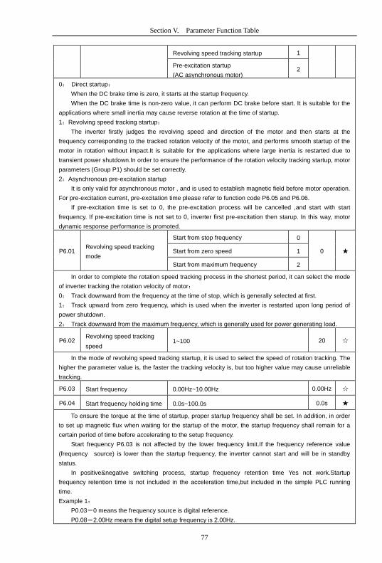
77
Section V. Parameter Function Table
Revolving speed tracking startup 1
Pre-excitation startup
(AC asynchronous motor) 2
0: Direct startup:
When the DC brake time is zero, it starts at the startup frequency.
When the DC brake time is non-zero value, it can perform DC brake before start. It is suitable for the
applications where small inertia may cause reverse rotation at the time of startup.
1:Revolving speed tracking startup:
The inverter firstly judges the revolving speed and direction of the motor and then starts at the
frequency corresponding to the tracked rotation velocity of the motor, and performs smooth startup of the
motor in rotation without impact.It is suitable for the applications where large inertia is restarted due to
transient power shutdown.In order to ensure the performance of the rotation velocity tracking startup, motor
parameters (Group P1) should be set correctly.
2:Asynchronous pre-excitation startup
It is only valid for asynchronous motor , and is used to establish magnetic field before motor operation.
For pre-excitation current, pre-excitation time please refer to function code P6.05 and P6.06.
If pre-excitation time is set to 0, the pre-excitation process will be cancelled ,and start with start
frequency. If pre-excitation time is not set to 0, inverter first pre-excitation then starup. In this way, motor
dynamic response performance is promoted.
P6.01 Revolving speed tracking
mode
Start from stop frequency 0
0 Start from zero speed 1
Start from maximum frequency 2
In order to complete the rotation speed tracking process in the shortest period, it can select the mode
of inverter tracking the rotation velocity of motor:
0: Track downward from the frequency at the time of stop, which is generally selected at first.
1: Track upward from zero frequency, which is used when the inverter is restarted upon long period of
power shutdown.
2: Track downward from the maximum frequency, which is generally used for power generating load.
P6.02 Revolving speed tracking
speed 1~100 20
In the mode of revolving speed tracking startup, it is used to select the speed of rotation tracking. The
higher the parameter value is, the faster the tracking velocity is, but too higher value may cause unreliable
tracking.
P6.03 Start frequency 0.00Hz~10.00Hz 0.00Hz
P6.04 Start frequency holding time 0.0s~100.0s 0.0s
To ensure the torque at the time of startup, proper startup frequency shall be set. In addition, in order
to set up magnetic flux when waiting for the startup of the motor, the startup frequency shall remain for a
certain period of time before accelerating to the setup frequency.
Start frequency P6.03 is not affected by the lower frequency limit.If the frequency reference value
(frequency source) is lower than the startup frequency, the inverter cannot start and will be in standby
status.
In positive&negative switching process, startup frequency retention time Yes not work.Startup
frequency retention time is not included in the acceleration time,but included in the simple PLC running
time.
Example 1:
P0.03=0 means the frequency source is digital reference.
P0.08=2.00Hz means the digital setup frequency is 2.00Hz.

78
Section V. Parameter Function Table
P6.03=5.00Hz means the startup frequency is 5.00Hz.
P6.04=2.0s means that the startup frequency retention time is 2.0s.
In this case, the inverter will be in the standby status and its output frequency is 0Hz.
Example 2:
P0.03=0 means the frequency source is digital reference.
P0.08=10.00Hz means the digital setup frequency is 10.00Hz.
P6.03=5.00Hz means the startup frequency is 5.00Hz.
P6.04=2.0s means that the startup frequency retention time is 2.0s.
In this case, the inverter accelerates to 5.00 Hz and remains for 2 seconds, and then accelerates to
the setup frequency 10Hz.
P6.05 Start dc braking current
/pre-excitation current 0%~100% 0%
P6.06 Start dc braking time /pre-
excitation time 0.0s~100.0s 0.0s
Pre-excitation is used to establish asynchronous motor magnetic field before startup, which would
improve response speed.
Start dc current braking is only valid when it is direct startup. Inverter first carries out dc braking
according to the setup of start dc current braking , and then carries out operation after start dc braking
time.
If dc braking time is set to 0, inverter directly start without dc braking. The bigger the dc braking current
is , the greater the braking force is.
If start mode is asynchrounous motor pre-excitation start, inverter first establish magnetic field through
pre-excitation current setup, then start to run after pre-excitation time. If set pre-excitation time to 0,
inverter would directly start without pre-excitation process./
Start dc braking current/pre-excitation current is the relative percentage of rated current.
P6.07 Acceleration/ deceleration
mode
Straight acc. /dec. 0
0
S curve acc. /dec. mode A 1
It is used to select the frequency change mode during the inverter start and stop process.
0: Straight acceleration/ deceleration
The output frequency increases or decreases along the straight line. HV590 series inverter provides 4
types of acceleration/deceleration time.It can select acceleration/ deceleration time via the multifunctional
digital input terminals.
1:S-curve acceleration/ deceleration mode A
The output frequency increases or decreases along the straight line. S curve is generally used in the
applications where start and stop processes are relatively gentle, such as elevator and conveyor belt.The
acceleration/ deceleration time is consistent with the straight acceleration/ deceleration time.Function
codes of P6.08 and P6.09 can be respectively definedthe time proportion of starting-segment and finishing-
segment for S-curve acceleration/ deceleration.
P6.08 Initial-segment time
proportion of S-curve 0.0%~(100.0%.P6.09) 30.0%
P6.09 Finishing-segment time
proportion of S-curve 0.0%~(100.0%.P6.08) 30.0%
Function code of P6.08 and P6.09 can be respectively defined the time proportion between the S-
curve initial-segment and finishing-segment for S-curve acceleration/ deceleration A. They are required to
meet the standard of P6.08+P6.09≤100.0%.
t1 in the Fig.5-11 is the parameters defined by P6.08, in this period of time which the changing slope
of output frequency is becoming larger and larger. t2 is defined by parameter P6.09, in this period of time

79
Section V. Parameter Function Table
which the changing slope of output frequency change to zero. The changing slope of output frequency is
fixing within the time of t1 and t2.
Fig.5-11S-curve acceleration/deceleration schematicdiagram A
P6.10 Stop mode Speed-Down to stop 0
0
Free stop 1
0:Deceleration to stop
When the stop command is valid, the inverter will decelerate to stop according to the setup
deceleration time.
1: Free stop
When the stop command is valid, the inverter will terminate the output immediately and the load will
coast to stop according to the mechanical inertia.
P6.11 DC braking initial frequency
at stop 0.00Hz~maximum frequency 0.00Hz
P6.12 DC braking waiting time at
stop 0.0s~36.0s 0.0s
P6.13 DC braking current at stop 0%~100% 0%
P6.14 DC braking time at stop 0.0s~100.0s 0.0s
DC brake initial frequency at stop: During the process of decelerating to stop, when the running
frequency at stop reaches this frequency, it will start the process of DC brake.
DC brake waiting time at stop: Prior to the beginning of DC brake at stop, the inverter will terminate
the output, and then start DC brake after this delay time. It is used to prevent over current fault due to DC
brake which starts at the time of higher velocity.
DC brake current at stop: The DC brake quantity added shall be set according to the percentage
setting of the rated current of the inverter. The higher the brake current is, more powerful the brake effect is.
DC brake time at stop: It refers to the continuous DC brake time. If this DC brake time is set to 0, it
indicates that there is no DC brake process, and the inverter will stop according to the setting process of
decelerating to stop.
The process of DC brake at stop is as shown in Figure below.
t1 t2 t2t1
t
Output frequency Hz
Setting frequency f

80
Section V. Parameter Function Table
Fig.5-13DC brake schematicdiagram
P6.15 Brake utilization ratio 0%~100% 100%
It is only valid for the inverter with built-in brake unit.
It is used to adjust the duty ratio of the brake unit.When the brake utilization ratio is high,then the duty
ratio of brake unit action is high,braking effect is strong.But there will be big fluctuation of inverter bus
voltage.
5.9 Keyboard and display:P7.00-P7.14
Code
Description/
Keyboard Display Setting Range
Factory
Setting
Change
Limit
P7.01 MF/REV key function selection
MF/REV key invalid 0
0
Switching between operation panel com-
mand channel&the remote command
channel (terminal command channel or
serial port command channel)
1
Switching between FWD&REV rotation 2
Forward jog command 3
Reverse jog command 4
It is used to set the functions of multifunctional MF/REV key.
0: Invalid function
1: Operation panel command channel and remote command channel
It can perform switching between the current command source and keyboard control(local
operation).The function key is invalid when current command source is keyboard control.
t
Output frequency
Hz
P6.11
t
Output voltage effective value
DC brake quantity at stop
Running command
P6.12
P6.14
81
Section V. Parameter Function Table
2: Switching between forward and reverse rotation
Switching the rotary direction of the motor via the MF/REV key on the keyboard is only enabled when
the command source is “operation panel command”.
3: Forward jog
It can perform forward jog (FJOG) operation via the MF/REV key on the keyboard.
4: Reverse jog
It can perform reverse jog (RJOG) operation via the MF/REV key on the keyboard.
P7.02 STOP/RESET function
The stop function of STOP/RES key is
valid only in the keyboard control mode. 0
1 The stop function of STOP/RES key is
valid in any control mode. 1
P7.03 LED running display
parameter1 0000~FFFF 1F
If the above parameters need to be displayed during the operation, users can set their corresponding
positions to 1 and then convert this binary number into decimal number and set it to P7.03.
P7.04 LED running display
parameter 2 0000~FFFF 0
If the above parameters need to be displayed during the operation, users can set their corresponding
positions to 1 and then convert this binary number into decimal number and set it to P7.04.
Running display parameter is used to set paratermers which can be seen under inverter running state.
32 state parameters can be checked at most,you could choose the needed state parameter through
P7.03、P7.04 binary digit,display sequence starts from P7.03 lowest digit order.
P7.05 LED stop display parameter 0000~FFFF 33
7 6 5 4 3 2 1 0
Running frequency 1(Hz)
Setting frequency (Hz)
Bus voltage(V)
Output voltage(V)
Output current(A)
Output power(kW)
Output torque(%)
DI input status(V)
15 14 13 12 11 10 9 8
D0 output status
Count value
Length value
Load speed display
PID setting
AI1(V)
AI2(V)
AI3(V)
7 6 5 4 3 2 1 0
PID feedback
Surplus running time
PLC stage
Input pulse frequency (kHz)
Running frequency 2(Hz)
AI1 voltage before correction(V)
AI2 voltage before correction(V)
AI3 voltage before correction(V)
15 14 13 12 11 10 9 8
Linear speed
Communication setting
Encoder feedback speed
Present power-on time(Hour)
Present running time(Min)
Input pulse frequency(Hz)
Main frequency X display
Auxiliary frequency Y display

82
Section V. Parameter Function Table
If the above parameters need to be displayed at the time of stop, it can set their corresponding
positions to 1 and then convert this binary number into decimal number and set it to P7.05.
P7.06 Load speed coefficient 0.0001~6.5000 1.0000
When display of the load speed is necessary, P7.06 is used to adjust the corresponding relationship
between inverter frequency output and load speed. For details please refer to P7.12.
P7.07 Inverter module radiator
temperature 0.0~100.0 12
It is used to display IGBT temperature.
Different model’s inverter module is set with different IGBT over temperature protection value.
P7.08 Product ID 0
Display inverter product ID
P7.09 Accumulative running time 0h~65535h 0h
It is used to display the accumulated running time of the inverter. When the accumulated running time
reaches P8.17 setup running time, the multifunctional digital output terminal(12) will output ON signal.
P7.10 Performance version
number Display performance version number -
P7.11 Software version No. Control board software version No. -
P7.12 Load speed display decimal
digits
No decimal place 0
1 One decimal place 1
Two decimal places 2
Three decimal places 3
Decimal point position: It is used to set the number of decimal places of the load speed.
For example, if the Load speed display coefficient P7.06 is 2.000,load speed display decimal digits is
2(Two decimal places),when inverter running frequency is 40.00Hz,the load speed will be :
40.00*2.000=80.00(2 decimal digit display)
If the inverter is in stopped state, then load speed displays as corresponding set frequency speed.Take
set frequency of 50.00Hz as an example,the stop state load speed is: 50.00*2.000=100.00(Two decimal
places)
P7.13 Accumulative power-on time 0h~65535h -
It displays accumulative power-on time since leaving the factory.
When it reaches the set power-on time (P8.17) , multi-function digital output (24) ON signal.
P7.14 Accumulative power
consumption 0~65535 -
7 6 5 4 3 2 1 0
DI input status
Setting frequency(Hz)
Bus voltage(V)
DO output status
AI1 (V)
AI2 (V)
AI3 (V)
Counter
15 14 13 12 11 10 9 8
Length value
Reserved
Reserved
Reserved
PLC stage
Load speed
PID setting
Input pulse frequency(Hz)

83
Section V. Parameter Function Table
It displays the inverter accumulative power consumption.
5.10 Auxiliary function:P8.00-P8.53
Code
Description/
Keyboard Display Setting Range
Factory
Setting
Change
Limit
P8.00 Jog running frequency 0.00Hz~maximum frequency 2.00Hz
P8.01 Jog acceleration time 0.0s~6500.0s 20.0s
P8.02 Jog deceleration time 0.0s~6500.0s 20.0s
It defines the reference frequency and acc. / dec. time of the inverter at the time of jogging.
The jog process is started and stopped according to direct startup mode(P6.00=0)and decelerate to
stop mode(P6.10=0).
P8.03 Acceleration time 2 0.0s~6500.0s 10.0s
P8.04 Deceleration time 2 0.0s~6500.0s 10.0s
P8.05 Acceleration time 3 0.0s~6500.0s 10.0s
P8.06 Deceleration time 3 0.0s~6500.0s 10.0s
P8.07 Acceleration time 4 0.0s~6500.0s 10.0s
P8.08 Deceleration time 4 0.0s~6500.0s 10.0s
HV590 offers 4 groups of speed-up/speed-down time,P0.17/P0.18 and 3 groups above.
P8.03 to P8.08 parameters have the same definition with P0.17 and P0.18.You can switch to choose
the 4 groups through different combination of DI multi-function digital input terminal.For specific using
method,please refer to function code P4.01~P4.05 for details.
P8.09 Hopping frequency 1 0.00Hz~maximum frequency 0.00Hz
P8.10 Hopping frequency 2 0.00Hz~maximum frequency 0.00Hz
P8.11 Hopping frequency amplitude 0.00Hz~maximum frequency 0.00Hz
Fig.5-14 Skip frequency schematicdiagram
When set frequency is within the range of hopping frequency,the actual running frequency will run
close to the set frequency of hopping frequency.Inverter can avoid load mechanical resonance by setting
hopping frequency.
HV590 can set 2 hopping frequency points,if both of them are set to 0,then the hopping frequency
function is canceled.Hopping frequency and hopping frequency amplitude schematic is shown in Fig5-14.
P8.12 Dead zone time of 0.00s~3000.0s 0.0s
Hopping frequency 1
Hopping frequency 2
Output frequency
Hz
Hopping frequency amplitude
t
Hopping frequency amplitude
Hopping frequency amplitude
Hopping frequency amplitude
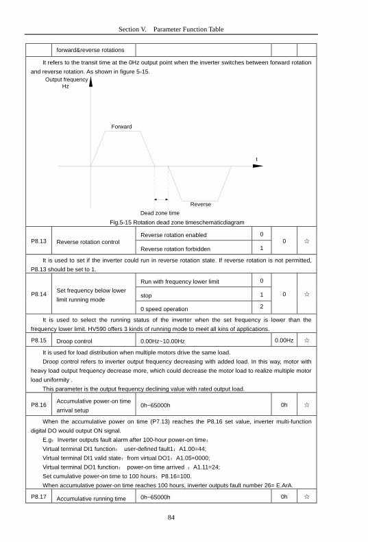
84
Section V. Parameter Function Table
forward&reverse rotations
It refers to the transit time at the 0Hz output point when the inverter switches between forward rotation
and reverse rotation. As shown in figure 5-15.
Fig.5-15 Rotation dead zone timeschematicdiagram
P8.13 Reverse rotation control Reverse rotation enabled 0
0
Reverse rotation forbidden 1
It is used to set if the inverter could run in reverse rotation state. If reverse rotation is not permitted,
P8.13 should be set to 1.
P8.14 Set frequency below lower
limit running mode
Run with frequency lower limit 0
0 stop 1
0 speed operation 2
It is used to select the running status of the inverter when the set frequency is lower than the
frequency lower limit. HV590 offers 3 kinds of running mode to meet all kins of applications.
P8.15 Droop control 0.00Hz~10.00Hz 0.00Hz
It is used for load distribution when multiple motors drive the same load.
Droop control refers to inverter output frequency decreasing with added load. In this way, motor with
heavy load output frequency decrease more, which could decrease the motor load to realize multiple motor
load uniformity .
This parameter is the output frequency declining value with rated output load.
P8.16 Accumulative power-on time
arrival setup 0h~65000h 0h
When the accumulative power on time (P7.13) reaches the P8.16 set value, inverter multi-function
digital DO would output ON signal.
E.g:Inverter outputs fault alarm after 100-hour power-on time:
Virtual terminal DI1 function: user-defined fault1:A1.00=44;
Virtual terminal DI1 valid state:from virtual DO1:A1.05=0000;
Virtual terminal DO1 function: power-on time arrived :A1.11=24;
Set cumulative power-on time to 100 hours:P8.16=100.
When accumulative power-on time reaches 100 hours, inverter outputs fault number 26= E.ArA.
P8.17 Accumulative running time 0h~65000h 0h
Output frequency
Hz
Forward
Reverse
Dead zone time
t
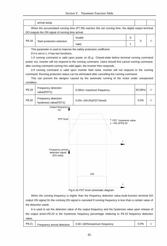
85
Section V. Parameter Function Table
arrival setup
When the accumulated running time (P7.09) reaches this set running time, the digital output terminal
DO outputs the ON signal of running time arrival.
P8.18 Start protection selection
Invalid 0
0
Valid 1
This parameter is used to improve the safety protection coefficient.
If it is set to 1, it has two functions:
1.If running command is valid upon power on (E.g:Closed-state before terminal running command
power on), inverter will not respond to the running command. Users should first cancel running command,
after running command coming into valid again, the inverter then responds.
2.If running command is valid upon inverter fault reset, inverter will not respond to the running
command. Running protection status can be eliminated after cancelling the running command.
This can prevent the dangers caused by the automatic running of the motor under unexpected
condition.
P8.19 Frequency detection
value(FDT1) 0.00Hz~maximum frequency 50.00Hz
P8.20 Frequency detection
hysteresis value(FDT1) 0.0%~100.0%(FDT1level) 5.0%
Fig.5-16 FDT level schematic diagram
When the running frequency is higher than the frequency detection value,multi-function terminal DO
output ON signal.On the contrary,ON signal is canceled if running frequency is less than a certain value of
the detection valule.
It is used to set the detection value of the output frequency and the hysteresis value upon release of
the output action.P8.20 is the hysteresis frequency percentage relativing to P8.19 frequency detection
value.
P8.21 Frequency arrival detection 0.00~100%maximum frequency 0.0%
Output frequency
Hz
t
Frequency arrival
detection signal
(DO,relay)
t
FDT hysteresis value
=P8.19*P8.20
FDT level
ON
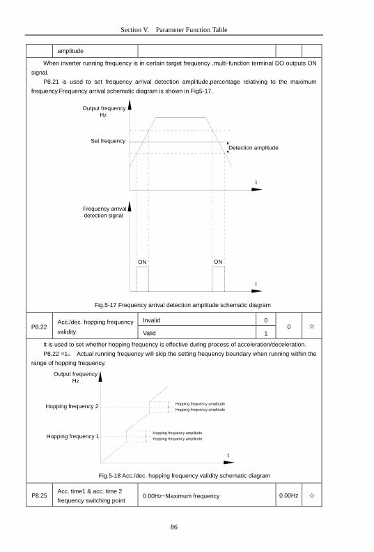
86
Section V. Parameter Function Table
amplitude
When inverter running frequency is in certain target frequency ,multi-function terminal DO outputs ON
signal.
P8.21 is used to set frequency arrival detection amplitude,percentage relativing to the maximum
frequency.Frequency arrival schematic diagram is shown in Fig5-17.
Fig.5-17 Frequency arrival detection amplitude schematic diagram
P8.22 Acc./dec. hopping frequency
validity
Invalid 0 0
Valid 1
It is used to set whether hopping frequency is effective during process of acceleration/deceleration.
P8.22 =1: Actual running frequency will skip the setting frequency boundary when running within the
range of hopping frequency.
Fig.5-18 Acc./dec. hopping frequency validity schematic diagram
P8.25 Acc. time1 & acc. time 2
frequency switching point 0.00Hz~Maximum frequency 0.00Hz
Output frequency
Hz
t
t
Set frequency
Detection amplitude
ON
ON
Frequency arrival
detection signal
Output frequency
Hz
t
Hopping frequency 1
Hopping frequency 2 Hopping frequency amplitude
Hopping frequency amplitude
Hopping frequency amplitude
Hopping frequency amplitude
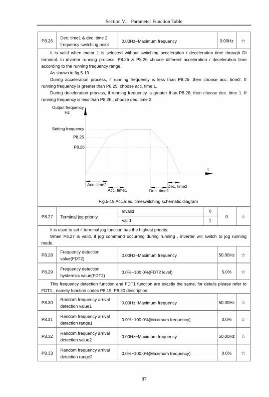
87
Section V. Parameter Function Table
P8.26 Dec. time1 & dec. time 2
frequency switching point 0.00Hz~Maximum frequency 0.00Hz
It is valid when motor 1 is selected without switching acceleration / deceleration time through DI
terminal. In inverter running process, P8.25 & P8.26 choose different acceleration / deceleration time
according to the running frequency range.
As shown in fig.5-19:
During acceleration process, if running frequency is less than P8.25 ,then choose acc. time2. If
running frequency is greater than P8.25, choose acc. time 1.
During deceleration process, if running frequency is greater than P8.26, then choose dec. time 1. If
running frequency is less than P8.26 , choose dec. time 2.
Fig.5-19 Acc./dec. timeswitching schematic diagram
P8.27 Terminal jog priority
Invalid 0
0 Valid 1
It is used to set if terminal jog function has the highest priority.
When P8.27 is valid, if jog command occurring during running , inverter will switch to jog running
mode.
P8.28 Frequency detection
value(FDT2) 0.00Hz~Maximum frequency 50.00Hz
P8.29 Frequency detection
hysteresis value(FDT2) 0.0%~100.0%(FDT2 level) 5.0%
This frequency detection function and FDT1 function are exactly the same, for details please refer to
FDT1 , namely function codes P8.19, P8.20 description.
P8.30 Random frequency arrival
detection value1 0.00Hz~Maximum frequency 50.00Hz
P8.31 Random frequency arrival
detection range1 0.0%~100.0%(Maximum frequency) 0.0%
P8.32 Random frequency arrival
detection value2 0.00Hz~Maximum frequency 50.00Hz
P8.33 Random frequency arrival
detection range2 0.0%~100.0%(Maximum frequency) 0.0%
Output frequency
Hz
Acc. time2
Acc. time1 Dec. time1 Dec. time2
t
Setting frequency
P8.25
P8.26

88
Section V. Parameter Function Table
Fig.5-20 Random frequency arrival detection schematic diagram
When inverter output frequency is within the positive & negative detection range of random frequency
arrival detection value , multi-funtion terminal DO output ON signal.
P8.34 Zero-current detection level 0.0%~300.0%(Motor rated current) 5.0%
P8.35 Zero-current detection delay
time 0.00s~600.00s 0.10s
When inverter output current is less than or equals to zero-current detection level, and the lasting
time exceeds zero-current detection delay time,inverter multi-function terminal DO output DO signal.
Fig.5-21 is schematic diagram of zero-current detection.
Fig.5-21 Zero-current detection schematic diagram
Running frequency
t
Random frequency arrival
Random frequency arrival
detection signal or relay
ON
ON
OFF
OFF
OFF
Frequency detection range
Frequency detection range
Output current
Zero current
detection signal
t
t
ON
P8.34
P8.35

89
Section V. Parameter Function Table
P8.36 Output current overlimit value 0.0%(No detection)
0.1%~300.0%(Motor rated current) 200.0%
P8.37 Output current overlimit
detection delay time 0.00s~600.00s 0.00s
Fig.5-22 Output current overlimit detection schematic diagram
When inverter output current is larger than output current overlimit value(P8.36) ,and lasting time
exceeds the software overlimit detection delay time ,inverter multi-function terminal DO output ON signal,
fig.5-22 is schematic diagram of output current overlimit detection.
P8.38 Random currentarrival 1 0.0%~300.0%(Motor rated current) 100.0%
P8.39 Random current arrival range1 0.0%~300.0%(Motor rated current) 0.0%
P8.40 Random currentarrival 2 0.0%~300.0%(Motor rated current) 100.0%
P8.41 Random currentarrival range2 0.0%~300.0%(Motor rated current) 0.0%
When inverter output current is within the positive & negative detection range of random arrival current
value , multi-funtion terminal DO output ON signal.
HV590 offers two groups of random current arrival range detection parameters ,as shown in fig. 5-23.
Output current
Output current overlimit
detection signal
t
t
P8.36
ON
P8.37
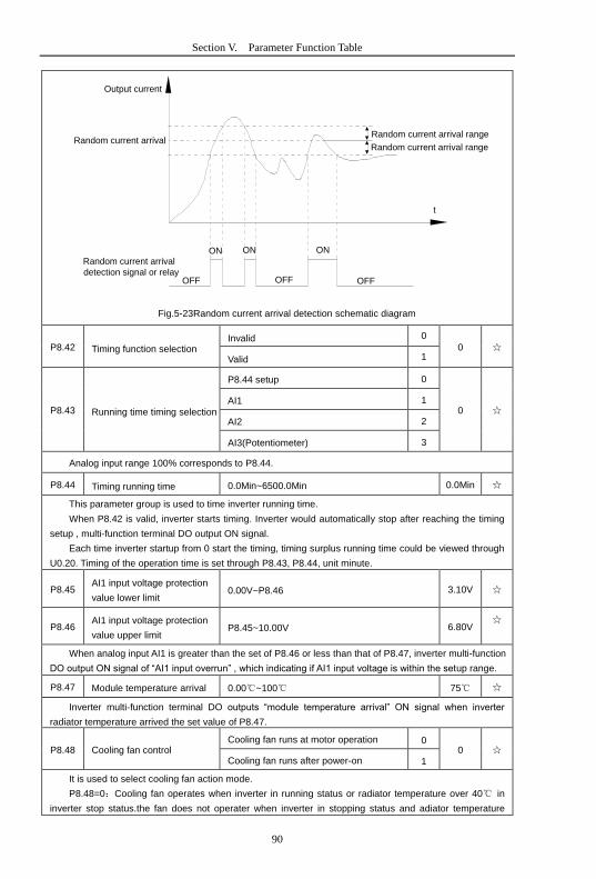
90
Section V. Parameter Function Table
Fig.5-23Random current arrival detection schematic diagram
P8.42 Timing function selection Invalid 0
0
Valid 1
P8.43 Running time timing selection
P8.44 setup 0
0 AI1 1
AI2 2
AI3(Potentiometer) 3
Analog input range 100% corresponds to P8.44.
P8.44 Timing running time 0.0Min~6500.0Min 0.0Min
This parameter group is used to time inverter running time.
When P8.42 is valid, inverter starts timing. Inverter would automatically stop after reaching the timing
setup , multi-function terminal DO output ON signal.
Each time inverter startup from 0 start the timing, timing surplus running time could be viewed through
U0.20. Timing of the operation time is set through P8.43, P8.44, unit minute.
P8.45 AI1 input voltage protection
value lower limit 0.00V~P8.46 3.10V
P8.46 AI1 input voltage protection
value upper limit P8.45~10.00V 6.80V
When analog input AI1 is greater than the set of P8.46 or less than that of P8.47, inverter multi-function
DO output ON signal of “AI1 input overrun” , which indicating if AI1 input voltage is within the setup range.
P8.47 Module temperature arrival 0.00~100 75
Inverter multi-function terminal DO outputs “module temperature arrival” ON signal when inverter
radiator temperature arrived the set value of P8.47.
P8.48 Cooling fan control Cooling fan runs at motor operation 0
0 Cooling fan runs after power-on 1
It is used to select cooling fan action mode.
P8.48=0:Cooling fan operates when inverter in running status or radiator temperature over 40 in
inverter stop status.the fan does not operater when inverter in stopping status and adiator temperature
Output current
t
Random current arrival
ON
ON
ON
OFF
OFF
OFF
Random current arrival range
Random current arrival range
Random current arrival
detection signal or relay
91
Section V. Parameter Function Table
below 40
P8.48=1:Cooling fan is always running after power-on.
P8.49 Wakeup frequency Sleep frequency(P8.51) ~maximum frequency
(P0.10) 0.00Hz
P8.50 Wakeup delay time 0.0s~6500.0s 0.0s
P8.51 Sleep frequency 0.00Hz~wake-up frequency(P8.49) 0.00Hz
P8.52 Sleep delay time 0.0s~6500.0s 0.0s
This group of function codes are used to realize sleep and wake up function.
During operation:when set frequency is less than or equals to sleep frequency(P8.51), inverter would
step into sleep state and stop after sleep delay time(P8.52).
If inverter is in sleep state and current running command is valid, when set frequency is no less than
P8.49 wake-up frequency, inverter will start to run after P8.50 wake-up delay time.
Generally, please set wake-up frequency no less than sleep frequency. Sleep function and wake-up
function are valid when both wake-up frequency and sleep frequency are set to 0.00 Hz.
When enabling sleep function(frequency source :PID) , PID calculation selection in sleep state is
influenced by function code PA.28(PA.28=1).
P8.53 The running time arrival 0.0Min~6500.0Min 0.0Min
When the running time reached the P8.53 set value, inverter multi-function DO output “Then running
time arrival” ON signal.
5.11 Overload and protection:P9.00-P9.70
Code
Description/
Keyboard Display Setting Range
Factory
Setting
Change
Limit
P9.00 Motor over load protection
selection
Invalid 0 1
Valid 1
P9.01 Motor overload protection
gain 0.20~10.00 1.00
P9.00=0: Without motor overload protection function. It is recommended to install a thermal relay
between the motor and the inverter.
P9.00=1: The inverter has overload protection function for the motor according to motor overload
protection inverse time limit curve.
Motor overload protection inverse time limit curve: 220%×(P9.01)× motor rated current,it will report
motor overload fault after it lasts for one minute. When the operating current of the motor reaches the
current of 150%×(P9.01)times the rated current of the motor, it will report motor overload after it lasts 60
minutes.
Users can set value of P9.01 according to the motor actual overload ability.If the parameter is set too
big, it may cause danger of motor overheating damage without inverter fault report.
P9.02 Motor overload pre-alarm
coefficient 50%~100% 80%
This function is used before motor overload fault by giving pre-alarm signal through multi-function
terminal DO.This pre-alarm coefficient is used to determine the warning timing before motor overload
protection. The higher the value,the shorter the warning timing will be.
When the inverter output current is accumulated more than the product of inverse time limit curve with
P9.02,multi-function terminal DO output “Motor overload pre-alarm”ON signal.
P9.03 Over-voltage stall gain 0(no over-voltage stall)~100 0
92
Section V. Parameter Function Table
P9.04 Over-voltage stall protection
voltage 120%~150%(3 phase) 130%
Over voltage stall: When the output voltageof the inverter reaches setup of over voltage stall
protection voltage (P9.04), if the inverter is running with acceleration speed, it will stop acceleration. When
the inverter is running with constant speed, it will reduce the output frequency. When the inverter is running
with deceleration speed, it will stop deceleration and the operating frequency will not recover normally till
the current is less than the current stall protection current (P9.04).
Over voltage stall protection voltage: It selects the protection point for over current stall function.
When the value is exceeded, the inverter starts to execute the over voltage stall protection function. This
value is relative to the percentage of rated voltageof the motor.
Overvoltage stall gain: It adjusts the inverter’s capacity in suppressing the voltage stall. The bigger
the value is, the stronger the capacity is. For the load with small inertia, the value should be small.
Otherwise, the dynamic response of the system would be slow. For the load with large inertia, the value
should be large. Otherwise, the suppressing result will be poor, and over voltage fault may be caused.
When the voltage stall gain is set to 0, the inverter starts to execute the over voltage stall protection
function.
P9.05 Over current stall gain 0~100 20
P9.06 Over current stall protection
current 100%~200% 150%
Over current stall: When the output current of the inverter reaches setup of over current stall
protection current (P9.06), if the inverter is running with acceleration speed, it will stop acceleration. When
the inverter is running with constant speed, it will reduce the output frequency. When the inverter is running
with deceleration speed, it will stop deceleration and the operating frequency will not recover normally till
the current is less than the current stall protection current (P9.06).
Over current stall protection current: It selects the protection point for over current stall function.
When the value is exceeded, the inverter starts to execute the over current stall protection function. This
value is relative to the percentage of rated current of the motor.
Over current stall gain: It adjusts the inverter’s capacity in suppressing the over current stall. The
bigger the value is, the stronger the capacity is. the stronger the capacity is. For the load with small inertia,
the value should be small. Otherwise, the dynamic response of the system would be slow. For the load with
large inertia, the value should be large. Otherwise, the suppressing result will be poor, and over currentfault
may be caused.
When the current stall gain is set to 0, the inverter starts to execute the over voltage stall protection
function.
P9.07 Ground short circuit protection
upon power-on
Invalid 0 1
Valid 1
It determines whether the motor has ground short circuit fault upon power-on. If this function is valid,
the inverter UVW end will output voltage within the period of time after power-on.
P9.09 Fault auto reset times 0~20 0
When the inverter selects fault auto reset, it is used to set the times of auto reset. If this value is
exceeded, the inverter will perform fault protection.
P9.10 Fault auto reset FAULT DO
selection
No action 0 0
Action 1
If inverter has been set of fault auto reset function , P9.10 is used to set if FAULT DO actions or not
during fault auto reset time.

93
Section V. Parameter Function Table
P9.11 Fault auto reset interval 0.1s~100.0s 1.0s
The waiting time of the inverter from the fault alarm to auto reset.
P9.12 Input phase lack protection
selection
1bit Input phase lack protection selection
11
Forbidden 0
Allowed 1
10bit Contactor attracting protection
Forbidden 0
Allowed 1
1bit:It is used to choose whether to protect input phase loss.
10bit:Contactor attracting protection
HV590 series inverter above 132kW (type G) has input phase fault protection function.For the inverter
below 132kW (type P), the input phase fault protection function is invalid at any setup.
P9.13 Output phase lack protection
selection
Invalid 0 1
valid 1
It is used to choose whether to protect output open-phase.
P9.14 The first fault type 0~99 -
P9.15 The second fault type 0~99 -
P9.16 The latest fault type 0~99 -
It records the latest 3 fault types for the inverter: 0 means no fault and 1 to 99 correspond to refer to
Chapter 6 for the details.
Table of fault type :
No. Fault display Fault type
0 Reserved No fault
1 1=Err01 Reserved
2 2= Err02 Acceleration over current
3 3= Err03 Deceleration over current
4 4=Err04 Constant speed over current
5 5=Err05 Acceleration over voltage
6 6= Err06 Deceleration over voltage
7 7=Err07 Constant speed over voltage
8 8=Err08 Control power supply fault
9 9=Err09 Undervoltage fault
10 10=Err10 Inverter overload
11 11= Err11 Motor overload
12 12= Err12 Input phase lack
13 13= Err13 Output phase lack
14 14= Err14 Module overheating
15 15= Err15 External equipment fault
16 16= Err16 Communication fault

94
Section V. Parameter Function Table
17 17=Err17 Contactor fault
18 18= Err18 Current inspection fault
19 19= Err19 Motor tuning fault
20 20= Err20 Encoder /PG card fault
21 21= Err21 EEPROM read & write fault
22 22= Err22 Inverter hardware fault
23 23= Err23 Short circuit to ground fault
24 Reserved Reserved
25 Reserved Reserved
26 26= Err26 Total running time arrival fault
27 27= Err27 User-defined fault 1
28 28=Err28 User-defined fault 2
29 29=Err29 Total power-on time arrival fault
30 30= Err30 Load off fault
31 31= Err31 PID feedback loss during operation fault
40 40= Err40 Each wave current limiting fault
41 41=Err41 Motor switching fault
42 42= Err42 Excessive speed deviation fault
43 43= Err43 Motor overspeed fault
45 45=Err45 Motor overtemperature fault
51 51= Err51 Initial position fault
P9.17 Third fault frequency The latest fault frequency
P9.18 Third fault current The latest fault current
P9.19 Third fault bus voltage The latest fault bus voltage
P9.20 Third fault input terminal
The latest fault digital input terminal status, order as below:
When input terminal status is ON, it’s corresponding
binary digit is 1. OFF corresponds to 0. All DI status are
converted to decimal display.
P9.21 Third fault output terminal
The latest fault digital output terminal status, order as
below :
When output terminal status is ON, it’s corresponding
binary digit is 1. OFF corresponds to 0. All status are
converted to decimal display.
BIT9 BIT8 BIT7 BIT6 BIT5 BIT4 BIT3 BIT2 BIT1 BIT0
DI1 DI2 DI3 DI4 DI5 DI6 DI7 DI8 DI9 DI0
BIT4 BIT3 BIT2 BIT1 BIT0
FMP REL1 REL2 DO1 DO2

95
Section V. Parameter Function Table
P9.22 Third fault inverter state Reserved
P9.23 Third fault power-on time The latest fault power-on time
P9.24 Third fault running time The latest fault running time
P9.27 Second fault frequency The latest fault frequency
P9.28 Second fault current The latest fault current
P9.29 Second fault bus voltage The latest fault bus voltage
P9.30 Second fault input terminal
The latest fault digital input terminal status, order as
below :
When input terminal status is ON, it’s corresponding
binary digit is 1. OFF corresponds to 0. All DI status are
converted to decimal display.
P9.31 Second fault output terminal
The latest fault digital input terminal status, order as
below :
When output terminal status is ON, it’s corresponding
binary digit is 1. OFF corresponds to 0. All DO status
are converted to decimal display.
P9.32 Second fault inverter state Reserved
P9.33 Second fault power-on time The latest fault power-on time
P9.34 Second fault running time The latest fault running time
P9.37 First fault frequency The latest fault frequency
P9.38 First fault current The latest fault current
P9.39 First fault bus voltage The latest fault bus voltage
P9.40 First fault input terminal
The latest fault digital input terminal status, order as
below :
When input terminal status is ON, it’s corresponding
binary digit is 1. OFF corresponds to 0. All DI status are
converted to decimal display.
P9.41 First fault output terminal The latest fault digital input terminal status, order as
below :
BIT9 BIT8 BIT7 BIT6 BIT5 BIT4 BIT3 BIT2 BIT1 BIT0
DI1 DI2 DI3 DI4 DI5 DI6 DI7 DI8 DI9 DI0
BIT4 BIT3 BIT2 BIT1 BIT0
FMP REL1 REL2 DO1 DO2
BIT9 BIT8 BIT7 BIT6 BIT5 BIT4 BIT3 BIT2 BIT1 BIT0
DI1 DI2 DI3 DI4 DI5 DI6 DI7 DI8 DI9 DI0
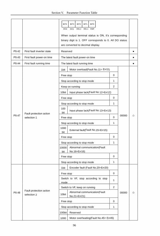
96
Section V. Parameter Function Table
When output terminal status is ON, it’s corresponding
binary digit is 1. OFF corresponds to 0. All DO status
are converted to decimal display.
P9.42 First fault inverter state Reserved
P9.43 First fault power-on time The latest fault power-on time
P9.44 First fault running time The latest fault running time
P9.47 Fault protection action
selection 1
1bit Motor overload(Fault No.11= Err11)
00000
Free stop 0
Stop according to stop mode 1
Keep on running 2
10bit Input phase lack(Fault No 12=Err12)
Free stop 0
Stop according to stop mode 1
100
bit Input phase lack(Fault No 13=Err13)
Free stop 0
Stop according to stop mode 1
1000
bit External fault(Fault No.15=Err15)
Free stop 0
Stop according to stop mode 1
10000
bit
Abnormal communication(Fault
No.16=Err16)
Free stop 0
Stop according to stop mode 1
P9.48 Fault protection action
selection 2
1bit Encoder fault (Fault No.20=Err20)
00000
Free stop 0
Switch to VF, stop according to stop
mode 1
Switch to VF, keep on running 2
10bit Abnormal communication(Fault
No.21=Err21)
Free stop 0
Stop according to stop mode 1
100bit Reserved
1000 Motor overheating(Fault No.45= Err45)
BIT4 BIT3 BIT2 BIT1 BIT0
FMP REL1 REL2 DO1 DO2
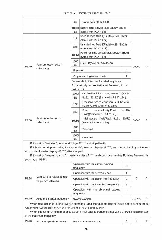
97
Section V. Parameter Function Table
bit (Same with P9.47 1 bit)
10000
bit
Runing time arrival(Fault No.26= Err26)
(Same with P9.47 1 bit)
P9.49 Fault protection action
selection 3
1bit User-defined fault 1(Fault No.27= Err27)
(Same with P9.47 1 bit)
00000
10bit User-defined fault 2(Fault No.28= Err28)
(Same with P9.47 1 bit)
100bit Power-on time arrival(Fault No.29= Err29)
(Same with P9.47 1 bit)
1000
bit Load off(Fault No.30= Err30)
Free stop 0
Stop according to stop mode 1
Decelerate to 7% of motor rated frequency.
Automatically recover to the set frequency if
no load off.
2
10000
bit
PID feedback lost during operation(Fault
No.31= Err31) (Same with P9.47 1 bit)
P9.50 Fault protection action
selection 4
1bit Excessive speed deviation(Fault No.42=
Err42) (Same with P9.47 1 bit)
00000
10bit Motor supervelocity(Fault No.43=
Err43)(Same with P9.47 1 bit)
100bit Initial position fault(Fault No.51= Err51)
(Same with P9.47 1 bit)
1000
bit Reserved
10000
bit Reserved
If it is set to “free stop”, inverter displays E.****,and stop directly.
If it is set to “stop according to stop mode”, inverter displays A.****, and stop according to the set
stop mode. Inverter displays E.**** after stopped.
If it is set to “keep on running”, inverter displays A.**** and continues running. Running frequency is
set through P9.54.
P9.54 Continued to run when fault
frequency selection
Operation with the current running
frequency 0
0
Operation with the set frequency 1
Operation with the upper limit frequency 2
Operation with the lower limit frequency 3
Operation with the abnormal backup
frequency 4
P9.55 Abnormal backup frequency 60.0%~100.0% 100.0%
When fault occuring during inverter operation , and the fault processing mode set to continu ing to
run, inverter would display A** and run with the P9.54 set frequency.
When choosing running frequency as abnormal backup frequency, set value of P9.55 is percentage
of the maximum frequency.
P9.56 Motor temperature sensor No temperature sensor 0 0
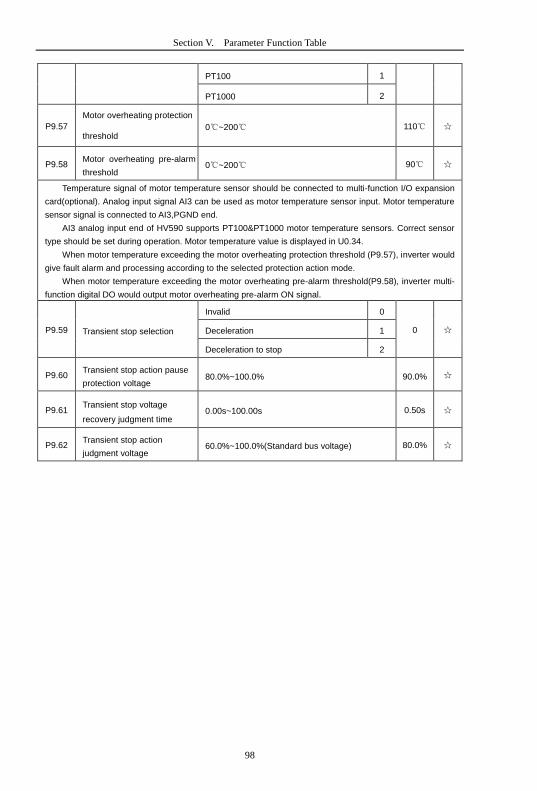
98
Section V. Parameter Function Table
PT100 1
PT1000 2
P9.57
Motor overheating protection
threshold 0~200 110
P9.58 Motor overheating pre-alarm
threshold 0~200 90
Temperature signal of motor temperature sensor should be connected to multi-function I/O expansion
card(optional). Analog input signal AI3 can be used as motor temperature sensor input. Motor temperature
sensor signal is connected to AI3,PGND end.
AI3 analog input end of HV590 supports PT100&PT1000 motor temperature sensors. Correct sensor
type should be set during operation. Motor temperature value is displayed in U0.34.
When motor temperature exceeding the motor overheating protection threshold (P9.57), inverter would
give fault alarm and processing according to the selected protection action mode.
When motor temperature exceeding the motor overheating pre-alarm threshold(P9.58), inverter multi-
function digital DO would output motor overheating pre-alarm ON signal.
P9.59 Transient stop selection
Invalid 0
0 Deceleration 1
Deceleration to stop 2
P9.60 Transient stop action pause
protection voltage 80.0%~100.0% 90.0%
P9.61 Transient stop voltage
recovery judgment time 0.00s~100.00s 0.50s
P9.62 Transient stop action
judgment voltage 60.0%~100.0%(Standard bus voltage) 80.0%
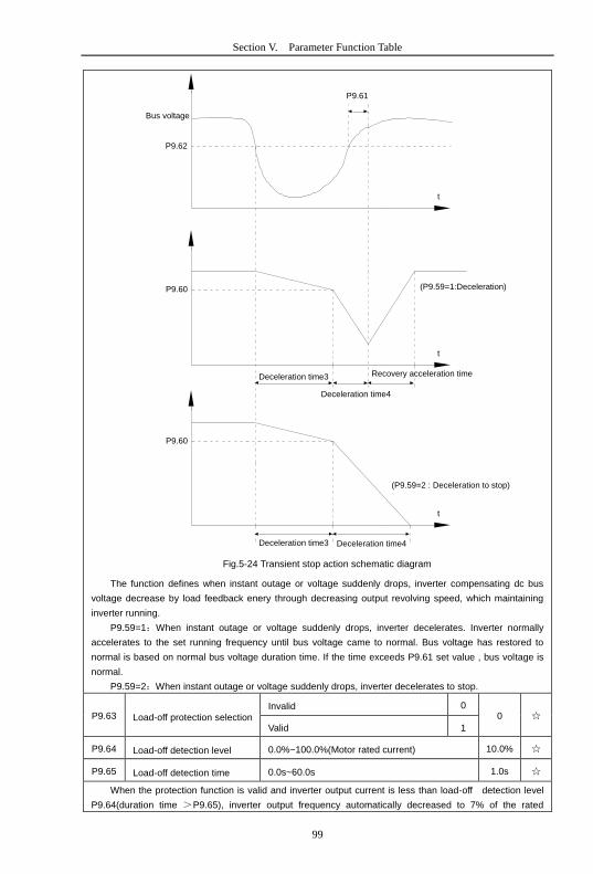
99
Section V. Parameter Function Table
Fig.5-24 Transient stop action schematic diagram
The function defines when instant outage or voltage suddenly drops, inverter compensating dc bus
voltage decrease by load feedback enery through decreasing output revolving speed, which maintaining
inverter running.
P9.59=1:When instant outage or voltage suddenly drops, inverter decelerates. Inverter normally
accelerates to the set running frequency until bus voltage came to normal. Bus voltage has restored to
normal is based on normal bus voltage duration time. If the time exceeds P9.61 set value , bus voltage is
normal.
P9.59=2:When instant outage or voltage suddenly drops, inverter decelerates to stop.
P9.63 Load-off protection selection
Invalid 0 0
Valid 1
P9.64 Load-off detection level 0.0%~100.0%(Motor rated current) 10.0%
P9.65 Load-off detection time 0.0s~60.0s 1.0s
When the protection function is valid and inverter output current is less than load-off detection level
P9.64(duration time >P9.65), inverter output frequency automatically decreased to 7% of the rated
Bus voltage
t
t
t
P9.62
P9.60 (P9.59=1:Deceleration)
P9.60
(P9.59=2 : Deceleration to stop)
P9.61
Deceleration time3
Deceleration time4
Recovery acceleration time
Deceleration time3 Deceleration time4

100
Section V. Parameter Function Table
frequency. In the load-off protection period, if the load restored, the inverter automatically restore to the set
running frequency.
P9.67 Over speed detection value 0.0%~50.0%(Maximum frequency) 20.0%
P9.68 Over speed detection time 0.0s~60.0s 1.0s
This function is only valid in speed sensor vector control.
Inverter fault alarm when motor actual revolving speed exceeds the set frequency(excess value >
P9.67 ,duration time >P9.68) .Fault No. 43=Err43.
P9.69 Excessive speed deviation
detection value 0.0%~50.0%(Maximum frequency) 20.0%
P9.70 Excessive speed deviation
detection time 0.0s~60.0s 5.0s
This function is only valid in speed sensor vector control.
Inverter fault alarms when deviation detected between motor actual revolving speed and the set
frequency(deviation>P9.69, duration time>P9.70). Fault No. 42=Err42.
P9.70=0.0s:Excessive speed deviation fault detection is canceled.
5.12 PID function group:PA.00-PA.28
PID control is a common method used in process control. Through the proportional,
integration and differential calculation on the difference between feedback signal and target signal
of the controlled parameter, PID control adjusts the output frequency of the inverter and forms
negative feedback system, making the controlled parameter stabilized on the target parameter.
PID control is appliedto several process controls such as flow control, pressure control and
temperature control.The schematic diagram for control is as shown in Fig. 5-25.
Fig.5-25PID process schematic diagram
Code
Description/
Keyboard Display Setting Range
Factory
Setting
Change
Limit
PA.00 PID reference source
PA.01 setup 0
0
AI1 1
AI2 2
AI3(Potentiometer) 3
PULSE(DI5) 4
Communication 5
MS command 6
+
- Target quantity
Feedback quantity
PID output control quantity
P
1
Td*s+1
1
Ti
1
S
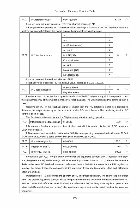
101
Section V. Parameter Function Table
PA.01 PIDreference value 0.0%~100.0% 50.0%
It is used to select target parameter reference channel of process PID.
Set target value of process PID is a relative value, set range is 0.0%~100.0%. PID feedback value is a
relative value as well,PID play the role of making the two relative value the same.
PA.02 PID feedback source
AI1 0
0
AI2 1
AI3(Potentiometer) 2
AI1-AI2 3
PULSE(DI5) 4
Communication 5
AI1+AI2 6
MAX(|AI1|,|AI2|) 7
MIN(|AI1|,|AI2|) 8
It is used to select the feedback channel of PID
Feedback value of process PID is a relative value, set range is 0.0%~100.0%.
PA.03 PID action direction Positive action 0
0
Negative action 1
Positive action: If the feedback signal is smaller than the PID reference signal, it is required to boost
the output frequency of the inverter to make PID reach balance. The winding tension PID control is such a
case.
Negative action: If the feedback signal is smaller than the PID reference signal, it is required to
decrease the output frequency of the inverter to make PID reach balance.The unwinding tension PID
control is such a case.
This function is influenced by function 35,please pay attention during operation.
PA.04 PID reference feedback range 0~65535 1000
PID reference feedback range is a dimensionless unit which is used to display U0.15 PID setup and
U0.16 PID feedback.
PID reference feedback related to the value 100.0%, corresponding to a given feedback range PA.04.If
PA.40 is set to 2000,PID is set to 100.0%,PID given display U0.15 is 2000.
PA.05 Proportional gain Kp1 0.0~100.0 20.0
PA.06 Integration time Ti1 0.01s~10.00s 2.00s
PA.07 Differential time Td1 0.00~10.000 0.000s
Proportional gain Kp1: the parameter determines the adjustable strength of PID regulator. The larger
P is, the greater the adjustable strength will be.When the parameter is set to 100.0, it means that when the
deviation between PID feedback value and reference value is 100.0%, the range for the PID regulator to
regulate the output frequency commands is the maximum frequency (integration effect and differential
effect are omitted).
Integration time Ti1:determines the strength of PID integration regulation. The shorter the integration
time , the greater adjustable strength will be.Integration time means that when the deviation between PID
feedback value and reference value is 100%, the adjustment by the integration regulator (proportional
effect and differential effect are omitted) after continuous adjustment in this period reaches the maximum
frequency.

102
Section V. Parameter Function Table
Differential time Td1: determines the degree of adjustment that PID regulator performs on the
derivation between PID feedback value and reference value.Differential time means that if the feedback
value changes100% within this time, the adjustment by the differential regulator (proportional effect and
differential effect are omitted) will reach the maximum frequency.The longer differential time is, the higher
the degree of adjustment will be.
PA.08 PID cutoff frequency of
reverse rotation 0.00~maximum frequency 2.00Hz
In some cases, only when the frequency of the PID output is negative (i.e., frequency inversion ) could
PID put the reference and feedback to the same state. High inversion frequency is not allowed in some
certain cases, PA.08 is used to determine reverse frequency upper limit.
PA.09 PID deviation limit 0.0%~100.0% 0.0%
It is used to set the maximum allowable deviation between the system feedback value and reference
value. When the deviation between the PID feedback and reference is within this range, the PID stops
adjustment. The deviation limit is calculated according to the percentage of the PID setup source (or
feedback source).When deviation between reference value and the feedback value is small,output
frequency is stability constant.It’s especially effective for some closed loop control occasions.
PA.10 PID differential amplitude
limit 0.00%~100.00% 0.10%
In PID regulation, the role of differential is relatively sensitive that system oscillation may be easily
caused. Therefore, range of PID differential regulation has been limited to a small range. PA.10 is used to
set PID differential output range.
PA.11 PID reference change duration 0.00s~650.00s 0.00s
PID reference changes according to this parameter value, which corresponds to the time taken for the
PID reference to change from 0% to 100%.
When PID reference changed,PID given value linear changes in accordance with given time,which can
reduce system adverse effect caused by given mutation.
PA.12 PID feedback filter time 0.00s~60.00s 0.00s
PA.13 PID output filter time 0.00s~60.00s 0.00s
PA.12 is used for filtering of PID feedback. The filtering helps to reduce the influence of the feedback
interference, but brings response performance of process closed-loop system.
PA.13 is used for filtering of PID output frequency. The filtering helps to reduce the mutations of the
output frequency, but brings response performance of process closed-loop system.
PA.14 Reserved - - -
PA.15 Proportional gain Kp2 0.0~100.0 20.0
PA.16 Integration time Ti2 0.01s~10.00s 2.00s
PA.17 Differential time Td2 0.00~10.000 0.000s
PA.18 PID parameter switching
condition
No switching 0
0 Switching through DI terminal 1
Switching through deviation 2
PA.19 PID parameter switching
deviation1 0.0%~PA.20 20.0%

103
Section V. Parameter Function Table
PA.20 PID parameter switching
deviation2 PA.19~100.0% 80.0%
Fig.5-26PID parameter switching schematic diagram
In some applications, one group of PID parameters can not meet the needs of the whole operation
process. Different parameters are used for different situations.
This group of function codes is used to switch 2 groups of PID parameters. Regulator parameters
PA.15~PA.17 and parameter PA.05~PA.07 have the same setting method.
Two groups of PID parameters can be switched through multi-function digital DI terminal as well as
PID deviation auto switching.
PA.18=1:Set multi-function terminal to 43(PID parameter switching terminal). Choose parameter
group 1(PA.05~PA.07) when terminal invalid,while valid please choose parameter group 2(PA.15~PA.17).
PA.18=2:When deviation absolute value between reference and feedback is less than PA.19 set
value, PID parameters select parameter group 1. When deviation absolute value between reference and
feedback is greater than PA.20 set value, PID parameters select group 2. When deviation absolute value
between reference and feedback is within the range of switching deviation 1 &2 , PID parameters select
linear interpolation value of the 2 PID parameter groups.As shown in 5-26.
PA.21 PID initial value 0.0%~100.0% 0.0%
PA.22 PID initial value retention time 0.00s~650.00s 0.00s
Inverter fixed startup value is PID initial value(PA.21) .PID starts closed-loop regulation after PID initial
value retention time(PA.22).
Fig.5-27 PID initial function schematic diagram
This function is used to limit difference between the PID output two beat (2ms/ beat ), which
PA.19 PA.20 PID deviation
PI parameter
PID parameter1
PA.05、PA.06、PA.07
PID parameter2
PA.15、PA.16、PA.17
Output frequency
Hz
t
PA.21
PA.22

104
Section V. Parameter Function Table
suppressing rapid change of PID output, so that the inverter operation tends to be stable.
PA.23 Output deviation forward
maximum value 0.00%~100.00% 1.00%
PA.24 Output deviation reverse
maximum value 0.00%~100.00% 1.00%
PA.23 and PA.24 correspond to the output deviation maximum absolute value of forward running and
reverse running respectively.
PA.25 PIDintegration attribute
1bit Integration separation
00
Invalid 0
Valid 1
10bit Whether stop integration when reaching
output limit
Continue integration 0
Stop integration 1
1bit :Integration separation
If integrationseparation valid, then when the multi-function digital DI integration suspended (function
22) effective, the PID integration stop operation, and only proportion and differential function effectively.
If integration separation invalid, regardless of validity of multi-function digital DI ,integration separation
is invalid.
10bit :Whether stop integration when reaching output limit
When PID operation output reaches the maximum or minimum value, user could choose whether to
stop integration or not.
If you choose to stop integration, then the PID integration stops calculation, which may contribute to
the reduction of PID overshoot.
PA.26 PID feedback loss detection
value
No judging 0.0% 0.0%
0.1%~100.0% 0.1%
PA.27 PID feedback loss detection
time 0.0s~20.0s 0s
This function is used to judge if PID feedback has been lost.
When PID feedback value is less than PA.26 set value, and lasted for more than PA.27 set value,
inverter fault alarm. Fault No. 31= Err31.
PA.28 PID stop operation
Stop without operation 0 0
Stop with operation 1
It is used to select if PID keeping operation under PID stop status. Generally PA.28=0 in stop status.
5.13 Swing frequency, fixed length and counting:Pb.00-Pb.09
The swing frequency function is applicable to textile and chemical fiber industries and
applications where traversing and winding functions are required.
Swing frequency means that the inverter output frequency swings up and down with the
setup frequency as the center, and the trace of running frequency at the time axis is as shown in
Fig. 5-28.The swing amplitude is set by Pb.00 and Pb.01.
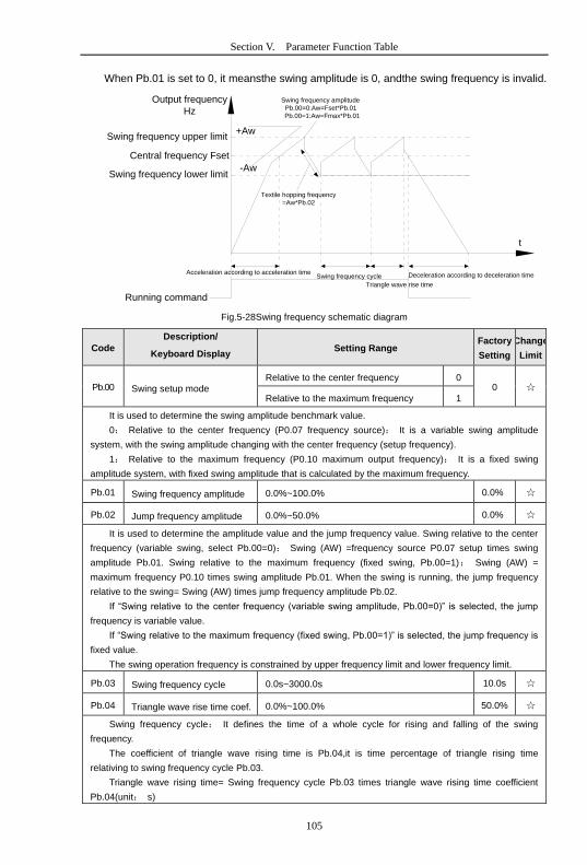
105
Section V. Parameter Function Table
When Pb.01 is set to 0, it meansthe swing amplitude is 0, andthe swing frequency is invalid.
Fig.5-28Swing frequency schematic diagram
Code
Description/
Keyboard Display Setting Range
Factory
Setting
Change
Limit
Pb.00 Swing setup mode Relative to the center frequency 0
0
Relative to the maximum frequency 1
It is used to determine the swing amplitude benchmark value.
0: Relative to the center frequency (P0.07 frequency source): It is a variable swing amplitude
system, with the swing amplitude changing with the center frequency (setup frequency).
1: Relative to the maximum frequency (P0.10 maximum output frequency): It is a fixed swing
amplitude system, with fixed swing amplitude that is calculated by the maximum frequency.
Pb.01 Swing frequency amplitude 0.0%~100.0% 0.0%
Pb.02 Jump frequency amplitude 0.0%~50.0% 0.0%
It is used to determine the amplitude value and the jump frequency value. Swing relative to the center
frequency (variable swing, select Pb.00=0): Swing (AW) =frequency source P0.07 setup times swing
amplitude Pb.01. Swing relative to the maximum frequency (fixed swing, Pb.00=1): Swing (AW) =
maximum frequency P0.10 times swing amplitude Pb.01. When the swing is running, the jump frequency
relative to the swing= Swing (AW) times jump frequency amplitude Pb.02.
If “Swing relative to the center frequency (variable swing amplitude, Pb.00=0)” is selected, the jump
frequency is variable value.
If “Swing relative to the maximum frequency (fixed swing, Pb.00=1)” is selected, the jump frequency is
fixed value.
The swing operation frequency is constrained by upper frequency limit and lower frequency limit.
Pb.03 Swing frequency cycle 0.0s~3000.0s 10.0s
Pb.04 Triangle wave rise time coef. 0.0%~100.0% 50.0%
Swing frequency cycle: It defines the time of a whole cycle for rising and falling of the swing
frequency.
The coefficient of triangle wave rising time is Pb.04,it is time percentage of triangle rising time
relativing to swing frequency cycle Pb.03.
Triangle wave rising time= Swing frequency cycle Pb.03 times triangle wave rising time coefficient
Pb.04(unit: s)
Output frequency
Hz
Swing frequency upper limit
Central frequency Fset
Swing frequency lower limit
Running command
Acceleration according to acceleration timeSwing frequency cycle
Triangle wave rise time
Deceleration according to deceleration time
t
+Aw
-Aw
Swing frequency amplitude
Pb.00=0:Aw=Fset*Pb.01
Pb.00=1:Aw=Fmax*Pb.01
Textile hopping frequency
=Aw*Pb.02
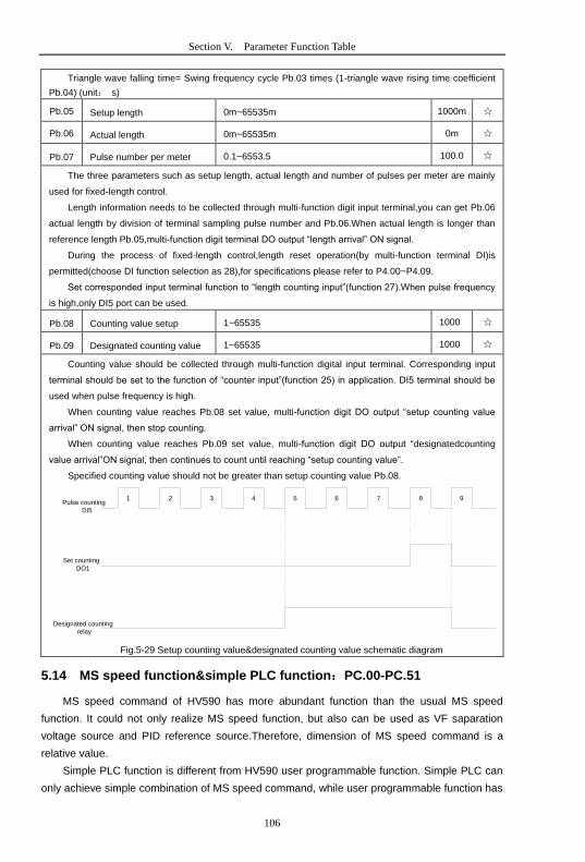
106
Section V. Parameter Function Table
Triangle wave falling time= Swing frequency cycle Pb.03 times (1-triangle wave rising time coefficient
Pb.04) (unit: s)
Pb.05 Setup length 0m~65535m 1000m
Pb.06 Actual length 0m~65535m 0m
Pb.07 Pulse number per meter 0.1~6553.5 100.0
The three parameters such as setup length, actual length and number of pulses per meter are mainly
used for fixed-length control.
Length information needs to be collected through multi-function digit input terminal,you can get Pb.06
actual length by division of terminal sampling pulse number and Pb.06.When actual length is longer than
reference length Pb.05,multi-function digit terminal DO output “length arrival” ON signal.
During the process of fixed-length control,length reset operation(by multi-function terminal DI)is
permitted(choose DI function selection as 28),for specifications please refer to P4.00~P4.09.
Set corresponded input terminal function to “length counting input”(function 27).When pulse frequency
is high,only DI5 port can be used.
Pb.08 Counting value setup 1~65535 1000
Pb.09 Designated counting value 1~65535 1000
Counting value should be collected through multi-function digital input terminal. Corresponding input
terminal should be set to the function of “counter input”(function 25) in application. DI5 terminal should be
used when pulse frequency is high.
When counting value reaches Pb.08 set value, multi-function digit DO output “setup counting value
arrival” ON signal, then stop counting.
When counting value reaches Pb.09 set value, multi-function digit DO output “designatedcounting
value arrival”ON signal, then continues to count until reaching “setup counting value”.
Specified counting value should not be greater than setup counting value Pb.08.
Fig.5-29 Setup counting value&designated counting value schematic diagram
5.14 MS speed function&simple PLC function:PC.00-PC.51
MS speed command of HV590 has more abundant function than the usual MS speed
function. It could not only realize MS speed function, but also can be used as VF saparation
voltage source and PID reference source.Therefore, dimension of MS speed command is a
relative value.
Simple PLC function is different from HV590 user programmable function. Simple PLC can
only achieve simple combination of MS speed command, while user programmable function has
1 2 3 4 5 6 7 8 9Pulse counting
DI5
Set counting
DO1
Designated counting
relay

107
Section V. Parameter Function Table
more abundant and practical uses. For specifications please refer to A7 group.
Code
Description/
Keyboard Display Setting Range
Factory
Setting
Change
Limit
PC.00 MS command 0 -100.0%~100.0% 0.0%
PC.01 MS command 1 -100.0%~100.0% 0.0%
PC.02 MS command 2 -100.0%~100.0% 0.0%
PC.03 MS command 3 -100.0%~100.0% 0.0%
PC.04 MS command 4 -100.0%~100.0% 0.0%
PC.05 MS command 5 -100.0%~100.0% 0.0%
PC.06 MS command 6 -100.0%~100.0% 0.0%
PC.07 MS command 7 -100.0%~100.0% 0.0%
PC.08 MS command 8 -100.0%~100.0% 0.0%
PC.09 MS command 9 -100.0%~100.0% 0.0%
PC.10 MS command 10 -100.0%~100.0% 0.0%
PC.11 MS command11 -100.0%~100.0% 0.0%
PC.12 MS command 12 -100.0%~100.0% 0.0%
PC.13 MS command 13 -100.0%~100.0% 0.0%
PC.14 MS command 14 -100.0%~100.0% 0.0%
PC.15 MS command 15 -100.0%~100.0% 0.0%
MS speed command can be used on three occasions:frequency source, VF saparation voltage
source, process PID set source.
Dimension of MS speed command is a relative value ranging from -100.0% to 100.0%. When used as
command source, it’s the percentage of maximum frequency. When used as VF saparation voltage source,
it’s the percentage of motor rated voltage. When used as PID set source, dimension conversion is not
needed during the process.
MS command should be selected according to the different states of multi-function digit DI terminals.
For details please refer to P4 group.
PC.16 PLC running mode
Single running stop 0
0 Single running end remaining final value 1
Continuous circulation 2
Simple PLC command can be used on two occasions:frequency source, VF saparation voltage source.
Fig 5-30 is the schematic diagram of simple PLC that used as frequency source. Positive & negative of
PC.00~PC.15 determines the running direction.
PLC has 3 running modes as frequency source(VF saparation voltage source is not provided with the
3 modes):
0: Single running stop
Upon completion of one single cycle of the inverter, it will stop automatically and will not start until
running command is given again.
1:Single running end remaining final value
Upon completion of one single cycle of the inverter, the inverter will remain the running frequency and
direction of last one phase. After the inverter restarted upon stop, it will run from the initial status of PLC.
108
Section V. Parameter Function Table
2: Continuous circulation
Upon completion of one single cycle of the inverter, it will enter next cycle and not stop until stop
command is given.
Fig.5-30Simple PLC schematic diagram
PC.17 PLC power off memory
selection
1bit Power off memory selection
00
Power off without memory 0
Power off with memory 1
10bit Stop memory selection
Stop without memory 0
Stop with memory 1
PLC power off memory refers to memorizing the PLC running stage and running frequency before
power off, and continues to run from the memory stage upon next power-on. If 1bit is set to 0, PLC process
would restart upon power-on.
PLC stop memory refers to the record of PLC running stage and running frequency of the time before.
Next time PLC continues to run from the memory stage. If 10bit is set to 0, PLC process would restart upon
power-on.
PC.18 PLC 0segment running time 0.0s(h) ~ 6553.5s(h) 0.0s(h)
PC.19 PLC 0segment acc./dec. time 0~3 0
PC.20 PLC 1segment running time 0.0s(h)~6553.5s(h) 0.0s(h)
PC.21 PLC 1segment acc./dec. time 0~3 0
PC.22 PLC 2segment running time 0.0s(h)~6553.5s(h) 0.0s(h)
PC.23 PLC 2segment acc./dec. time 0~3 0
Running direction
PC.19
PC.00
PC.21
PC.01
PC.18 PC.20 PC.23
PC.02PC.14
PC.15
250ms pulse
t
DO or RELAY output
109
Section V. Parameter Function Table
PC.24 PLC 3segment running time 0.0s(h)~6553.5s(h) 0.0s(h)
PC.25 PLC 3segment acc./dec. time 0~3 0
PC.26 PLC 4segment running time 0.0s(h)~6553.5s(h) 0.0s(h)
PC.27 PLC 4segment acc./dec. time 0~3 0
PC.28 PLC 5 segment running time 0.0s(h)~6553.5s(h) 0.0s(h)
PC.29 PLC 5segment acc./dec. time 0~3 0
PC.30 PLC 6segment running time 0.0s(h)~6553.5s(h) 0.0s(h)
PC.31 PLC 6segment acc./dec. time 0~3 0
PC.32 PLC 7segment running time 0.0s(h)~6553.5s(h) 0.0s(h)
PC.33 PLC 7segment acc./dec. time 0~3 0
PC.34 PLC 8segment running time 0.0s(h)~6553.5s(h) 0.0s(h)
PC.35 PLC 8segment acc./dec. time 0~3 0
PC.36 PLC 9segment running time 0.0s(h)~6553.5s(h) 0.0s(h)
PC.37 PLC 9segment acc./dec. time 0~3 0
PC.38 PLC 10segment running time 0.0s(h)~6553.5s(h) 0.0s(h)
PC.39 PLC 10segment acc./dec.time 0~3 0
PC.40 PLC 11segment running time 0.0s(h)~6553.5s(h) 0.0s(h)
PC.41 PLC 11segment acc./dec. time 0~3 0
PC.42 PLC 12segment running time 0.0s(h)~6553.5s(h) 0.0s(h)
PC.43 PLC 12segment acc./dec. time 0~3 0
PC.44 PLC 13segment running time 0.0s(h)~6553.5s(h) 0.0s(h)
PC.45 PLC 13segment acc./dec. time 0~3 0
PC.46 PLC 14segment running time 0.0s(h)~6553.5s(h) 0.0s(h)
PC.47 PLC 14segment acc./dec. time 0~3 0
PC.48 PLC 15segment running time 0.0s(h)~6553.5s(h) 0.0s(h)
PC.49 PLC 15segment acc./dec. time 0~3 0
PC.50 Running time unit S(second) 0
0 H(hour) 1
PC.51 MS command 0 reference
mode
Function code PC.00 reference 0
0
AI1 1
AI2 2
AI3(Potentiometer) 3
PULSE 4
PID 5
Preset frequency(P0.08) reference, 6
110
Section V. Parameter Function Table
UP/DOWN can be modified
It is used to select the reference channel of MS speed 0.
Besides choosing PC.00, MS command 0 has many other options, which is convenient for switching
between MS command and other set modes.
Both MS command and simple PLC used as frequency source can easily realize switching between
the two frequency sources.
5.15 Communication function group:Pd.00-Pd.06
Please refer to《HV590communication protocol》
Code
Description/
Keyboard Display Setting Range
Factory
Setting
Change
Limit
Pd.00 Baud rate
1bit MODBUS
6005
300BPS 0
600BPS 1
1200BPS 2
2400BPS 3
4800BPS 4
9600BPS 5
19200BPS 6
38400BPS 7
57600BPS 8
115200BPS 9
10bit Profibus-DP
115200BPS 0
208300BPS 1
256000BPS 2
512000BPS 3
100
bit Reserved
1000
bit Reserved
Pd.01 Data format
Without calibration (8-N-2) 0
0
Even parity calibration(8-E-1) 1
Uneven parity calibration(8-O-1) 2
8-N-1 3
Pd.02 Local address 1-247, 0 is broadcast address 1

111
Section V. Parameter Function Table
Pd.03 Response delay 0ms-20ms 2
Pd.04 Excessive communication
time 0.0(invalid), 0.1s-60.0s 0.0
Pd.05 Data transformat selection
1bit MODBUS
30
Non-standard MODBUS protocal 0
Standard MODBUS protocal 1
10
bit Profibus-DP
PPO1 format 0
PPO2 format 1
PPO3 format 2
PPO5 format 3
Pd.06 Communication read
current resolution
0.01A 0 0
0.1A 1
5.16 User customization function code:PE.00-PE.29
Code
Description/
Keyboard Display Setting Range
Factory
Setting
Change
Limit
PE.00 User function code 0 P0.00~PP.xx,A0.00~Ax.xx,U0.xx P0.01
PE.01 User function code 1 P0.00~PP.xx,A0.00~Ax.xx,U0.xx P0.02
PE.02 User function code 2 P0.00~PP.xx,A0.00~Ax.xx,U0.xx P0.03
PE.03 User function code 3 P0.00~PP.xx,A0.00~Ax.xx,U0.xx P0.07
PE.04 User function code 4 P0.00~PP.xx,A0.00~Ax.xx,U0.xx P0.08
PE.05 User function code 5 P0.00~PP.xx,A0.00~Ax.xx,U0.xx P0.17
PE.06 User function code 6 P0.00~PP.xx,A0.00~Ax.xx,U0.xx P0.18
PE.07 User function code 7 P0.00~PP.xx,A0.00~Ax.xx,U0.xx P3.00
PE.08 User function code 8 P0.00~PP.xx,A0.00~Ax.xx,U0.xx P3.01
PE.09 User function code 9 P0.00~PP.xx,A0.00~Ax.xx,U0.xx P4.00
PE.10 User function code 10 P0.00~PP.xx,A0.00~Ax.xx,U0.xx P4.01
PE.11 User function code 11 P0.00~PP.xx,A0.00~Ax.xx,U0.xx P4.02
PE.12 User function code 12 P0.00~PP.xx,A0.00~Ax.xx,U0.xx P5.04
PE.13 User function code 13 P0.00~PP.xx,A0.00~Ax.xx,U0.xx P5.07
PE.14 User function code 14 P0.00~PP.xx,A0.00~Ax.xx,U0.xx P6.00
PE.15 User function code 15 P0.00~PP.xx,A0.00~Ax.xx,U0.xx P6.10
112
Section V. Parameter Function Table
PE.16 User function code 16 P0.00~PP.xx,A0.00~Ax.xx,U0.xx P0.00
PE.17 User function code 17 P0.00~PP.xx,A0.00~Ax.xx,U0.xx P0.00
PE.18 User function code 18 P0.00~PP.xx,A0.00~Ax.xx,U0.xx P0.00
PE.19 User function code 19 P0.00~PP.xx,A0.00~Ax.xx,U0.xx P0.00
PE.20 User function code 20 P0.00~PP.xx,A0.00~Ax.xx,U0.xx P0.00
PE.21 User function code 21 P0.00~PP.xx,A0.00~Ax.xx,U0.xx P0.00
PE.22 User function code 22 P0.00~PP.xx,A0.00~Ax.xx,U0.xx P0.00
PE.23 User function code 23 P0.00~PP.xx,A0.00~Ax.xx,U0.xx P0.00
PE.24 User function code 24 P0.00~PP.xx,A0.00~Ax.xx,U0.xx P0.00
PE.25 User function code 25 P0.00~PP.xx,A0.00~Ax.xx,U0.xx P0.00
PE.26 User function code 26 P0.00~PP.xx,A0.00~Ax.xx,U0.xx P0.00
PE.27 User function code 27 P0.00~PP.xx,A0.00~Ax.xx,U0.xx P0.00
PE.28 User function code 28 P0.00~PP.xx,A0.00~Ax.xx,U0.xx P0.00
PE.29 User function code 29 P0.00~PP.xx,A0.00~Ax.xx,U0.xx P0.00
This function group is the user customization function code.
Users can put the required parameters (among all HV590 function codes) to the PE group as the user
customization function group.
PE group can offer 30 user customization function codes at most.When PE displays P0.00, it means
user function code is null.
In user customization function mode, display of the function codes is defined through PE.00~PE.31.
Sequence is consistent with the PE function codes, skip P0.00.
5.17 Function code management:PP.00-PP.04
Code
Description/
Keyboard Display Setting Range
Factory
Setting
Change
Limit
PP.00 User password 0~65535 0
The password set function is used to prohibit the unauthorized person from viewing and modifying
the parameters.
When the parameter is set to any non-zero number, the password protection function is enabled. If
no password is needed, change the parameter value to 00000.
After the user password is set and takes effect, when entering the password setting state, if the
user password is incorrect, you cannot view and modify the parameter. You can only view the operation
display parameters and stop displaying parameters.
Please keep your password in mind. If you set the password mistakenly orforget the password,
please contact the manufacturer.
PP.01 Parameter initialization
No function 0
0 Restore to factory default value,motor
parameter not included 1

113
Section V. Parameter Function Table
Clear memory 2
Restore factory parameters, Including
motor parameters 3
Backup user current parameter 4
Restore user backup parameter 501
0: No function.
1:Restore to factory default value,motor parameter not included
The inverter restores all the parameters excluding the following parameters of the factory default
values:
Motor parameters, P0.22, fault record information, P7.09, P7.13, P7.14.
2:Clear memory
The inverter clears the fault records , P7.09, P7.13 and P7.14 to zero.
3:Restore factory parameters, Including motor parameters
PP.01=3,The inverter restores all the parameters excluding the following parameters of the factory
default values
4:Backup user current parameter
It is the backup of user current setting parameters, which is convenient for the user to restore the
disordered parameters .
501:Restore user backup parameter
It is used to restore the backup of user parameters, that is, restore the backup parameters whichis
set through PP.01=501.
PP.02 Parameter display attribute
1bit U group display selection
11
No display 0
Display 1
10bit A group display selection
No display 0
Display 1
PP.03 Personalized parameter
display selection
1bit Custom parameter display selection
00
No display 0
Display 1
10bit User change parameter display selection
No display 0
Display 1
The establishment of parameter display selection is basically convenient for the users viewing the
different arrangement forms of function parameters according to the actual needs. Three display
methods are offered as below:
Name Discription
Function parameter mode Sequence display inverter function parameters, respectively
P0~PF、A0~AF、U0~UF.
User customization parameter User customization display of specified function
parameters(32 at most). The display parameters is
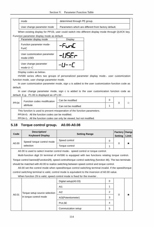
114
Section V. Parameter Function Table
mode determined through PE group.
User change parameter mode Parameters which are different from factory default.
When existing display for PP.03, user could switch into different display mode through QUICK key.
Function parameter display mode as default.
Parameter display mode Display
Function parameter mode-
FunC
User customization parameter
mode-USEt
User change parameter
mode-U--C
Display codes as below:
HV590 series offers two groups of personalized parameter display mode:user customization
function mode, user change parameter mode.
In user customization parameter mode, sign u is added to the user customization function code as
default.
In user change parameter mode, sign c is added to the user customization function code as
default. E.g:P1.00 is displayed as cP1.00 .
PP.04 Function codes modification
attribute
Can be modified 0
0
Can not be modified 1
This function is used to prevent misoperation of the function parameters.
PP.04=0:All the function codes can be modified.
PP.04=1:All the function codes can only be viewed, but not modified.
5.18 Torque control group: A0.00-A0.08
Code Description/
Keyboard Display Setting Range
Factory
Setting
Change
Limit
A0.00 Speed/ torque control mode
selection
Speed control 0 0
Torque control 1
A0.00 is used to select inverter control mode:speed control or torque control.
Multi-function digit DI terminal of HV590 is equipped with two functions relating torque control:
Torque control banned(Function29), speed control/torque control switching (function 46). The two terminals
should be matched with A0.00 to realize switching between speed control and torque control.
A0.00 set the control mode when speed/torque control switching terminal invalid. If the speed/torque
control switching terminal is valid, control mode is equivalent to the inversion of A0.00 value.
When function 29 is valid, speed control mode is fixed for the inverter .
A0.01 Torque setup source selection
in torque control mode
Digital setup(A0.03) 0
0
AI1 1
AI2 2
AI3(Potentiometer) 3
PULSE 4
Commuication setup 5

115
Section V. Parameter Function Table
MIN(AI1,AI2) 6
MAX(AI1,AI2) 7
A0.03 Torque digital setup in torque
control mode -200.0%~200.0% 150%
A0.01 is used to select torque set source. There are totally 8 kinds of torque set mode.
Torque set is a relative value, which 100% corresponding to inverter rated torque. Set range:
200.0%~200.0%.Maximum torque is 2 times that of inverter rated torque
When the torque is set by selection 1~7, 100% of communication ,analog input, pulse input
corresponding to A0.03.
A0.05 Torque control forward
maximum frequency 0.00Hz~Maximum frequency(P0.10) 50.00Hz
A0.06 Torque control reverse
maximum frequency 0.00Hz~Maximum frequency(P0.10) 50.00Hz
A0.05, A0.06 are used to set forward or reverse maximum running frequency in torque control mode.
In inverter toque control mode, if load torque is less than motor output toque, the motor revolving
speed would speed up. In case of galloping or other accidents of mechanical system , motor maximum
revolving speed must be limited.
A0.07 Torque control acc. time 0.00s~65000s 0.00s
A0.08 Torque control dec. time 0.00s~65000s 0.00s
In torque control mode , rate of speed change of motor and load is decided by the difference
between motor output toque and load torque. Therefore, motor speed may change fast, causing noise
or excessive mechanical stress problems. By setting the torque control acc./dec. time, can make the
motor speed changes smoothly.
A0.07 and A0.08 should be set to 0.00s in situations where torque rapid response is needed.
E.g:Two motors drive the same load, to make sure of load uniform distribution , one is set as host
inverter(speed control mode) and another is the slave one(torque control mode). Actual output torque of
the host inverter is the torque command of the slave, and slave torque is required to quickly follow the
host torque, then torque control acc./dec. time is set to 0.00s for the slave inverter.
5.19 VirtualIO: A1.00-A1.21
Code
Description/
Keyboard Display Setting Range
Factory
Setting
Change
Limit
A1.00 Virtual VDI1 function selection 0~59 0
A1.01 Virtual VDI2 function selection 0~59 0
A1.02 Virtual VDI3 function selection 0~59 0
A1.03 Virtual VDI4 function selection 0~59 0
A1.04 Virtual VDI5 function selection 0~59 0
Functions of virtual VDI1~VDI5 are equal to DI terminals on control board. VDI1~VDI5 can be used
as multi-function digital input terminals, for details please refer to description of P4.00~P4.09 .
A1.05
Virtual VD1 terminal valid
state set mode
1bit Virtual VDI1
00000 State of virtual VYx decides whether
VDI is effective 0
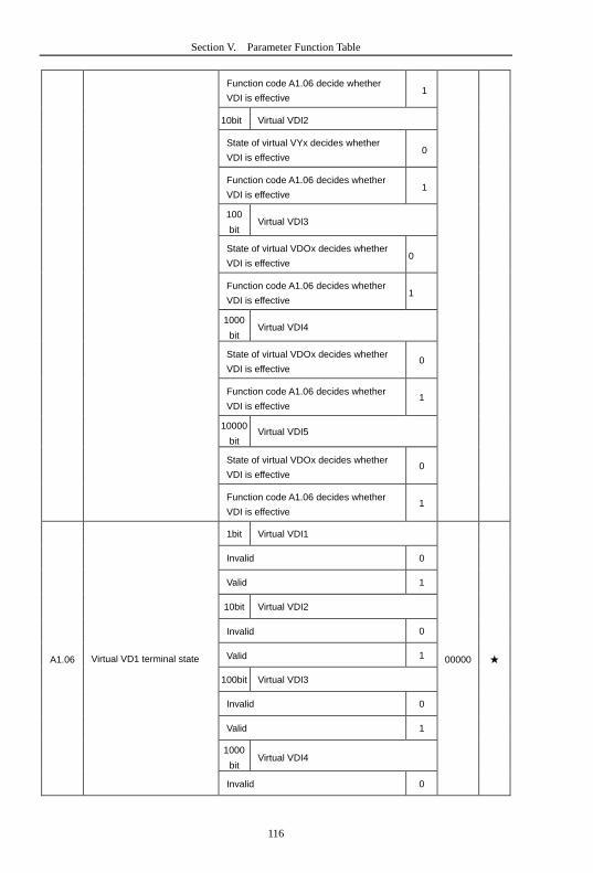
116
Section V. Parameter Function Table
Function code A1.06 decide whether
VDI is effective 1
10bit Virtual VDI2
State of virtual VYx decides whether
VDI is effective 0
Function code A1.06 decides whether
VDI is effective 1
100
bit Virtual VDI3
State of virtual VDOx decides whether
VDI is effective 0
Function code A1.06 decides whether
VDI is effective 1
1000
bit Virtual VDI4
State of virtual VDOx decides whether
VDI is effective 0
Function code A1.06 decides whether
VDI is effective 1
10000
bit Virtual VDI5
State of virtual VDOx decides whether
VDI is effective 0
Function code A1.06 decides whether
VDI is effective 1
A1.06 Virtual VD1 terminal state
1bit Virtual VDI1
00000
Invalid 0
Valid 1
10bit Virtual VDI2
Invalid 0
Valid 1
100bit Virtual VDI3
Invalid 0
Valid 1
1000
bit Virtual VDI4
Invalid 0
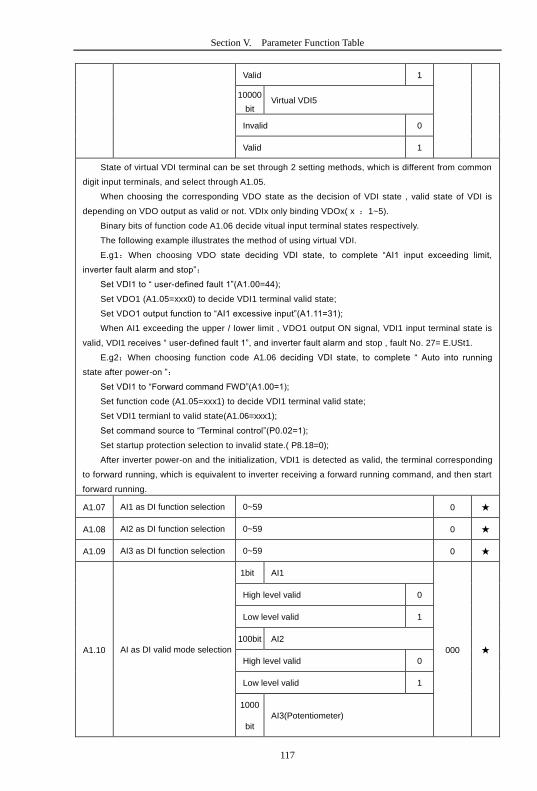
117
Section V. Parameter Function Table
Valid 1
10000
bit Virtual VDI5
Invalid 0
Valid 1
State of virtual VDI terminal can be set through 2 setting methods, which is different from common
digit input terminals, and select through A1.05.
When choosing the corresponding VDO state as the decision of VDI state , valid state of VDI is
depending on VDO output as valid or not. VDIx only binding VDOx( x :1~5).
Binary bits of function code A1.06 decide vitual input terminal states respectively.
The following example illustrates the method of using virtual VDI.
E.g1:When choosing VDO state deciding VDI state, to complete “AI1 input exceeding limit,
inverter fault alarm and stop”:
Set VDI1 to “ user-defined fault 1”(A1.00=44);
Set VDO1 (A1.05=xxx0) to decide VDI1 terminal valid state;
Set VDO1 output function to “AI1 excessive input”(A1.11=31);
When AI1 exceeding the upper / lower limit , VDO1 output ON signal, VDI1 input terminal state is
valid, VDI1 receives “ user-defined fault 1”, and inverter fault alarm and stop , fault No. 27= E.USt1.
E.g2:When choosing function code A1.06 deciding VDI state, to complete “ Auto into running
state after power-on ”:
Set VDI1 to “Forward command FWD”(A1.00=1);
Set function code (A1.05=xxx1) to decide VDI1 terminal valid state;
Set VDI1 termianl to valid state(A1.06=xxx1);
Set command source to “Terminal control”(P0.02=1);
Set startup protection selection to invalid state.( P8.18=0);
After inverter power-on and the initialization, VDI1 is detected as valid, the terminal corresponding
to forward running, which is equivalent to inverter receiving a forward running command, and then start
forward running.
A1.07 AI1 as DI function selection 0~59 0
A1.08 AI2 as DI function selection 0~59 0
A1.09 AI3 as DI function selection 0~59 0
A1.10 AI as DI valid mode selection
1bit AI1
000
High level valid 0
Low level valid 1
100bit AI2
High level valid 0
Low level valid 1
1000
bit
AI3(Potentiometer)

118
Section V. Parameter Function Table
High level valid 0
Low level valid 1
AI is used as DI for this function group. AI input voltage is greater than 7V, corresponding AI terminal
state is high level. AI input voltage is less than 3V, corresponding AI terminal state is low level. 3V~7V for
hysteresis loop .
Whether AI (as DI) high level valid or low level valid is determined through function code A1.10. For
AI(as DI) function settings, they are same with common DI settings, for details please refer to P4 group .
Fig. 5-31 takes AI input voltage as an example, explains the relationship between AI input voltage and
corresponding DI state:
Fig.5-31AI terminal valid state schematic diagram
A1.11 Virtual VDO1 output function
Short circuit with physics DIx internals 0
0 See P5 group for physics DO output
selection 1~40
A1.12 Virtual VDO2 output function
Short circuit with physics DIx internals 0
0 See P5 group for physics DO output
selection 1~40
A1.13 Virtual VDO3 output function
Short circuit with physics DIx internals 0
0 See P5 group for physics DO output
selection 1~40
A1.14 Virtual VDO4 output function
Short circuit with physics DIx internals 0
0 See P5 group for physics DO output
selection 1~40
A1.15 Virtual VDO5 output function
Short circuit with physics DIx internals 0
0 See P5 group for physics DO output
selection 1~40
A1.16 VDO1 output delay time 0.0s~3600.0s 0.0s
AI input voltage
t
DC7V
DC3V
ON
ON
OFF
AI terminal status

119
Section V. Parameter Function Table
A1.17 VDO2 output delay time 0.0s~3600.0s 0.0s
A1.18 VDO3 output delay time 0.0s~3600.0s 0.0s
A1.19 VDO4 output delay time 0.0s~3600.0s 0.0s
A1.20 VDO5 output delay time 0.0s~3600.0s 0.0s
A1.21 VDO output terminal valid
state selection
1bit VDO1
00000
Positive logic 0
Negative logic 1
10bit VDO2
Positive logic 0
Negative logic 1
100bit VDO3
Positive logic 0
Negative logic 1
1000
bit VDO4
Positive logic 0
Negative logic 1
10000
bit VDO5
Positive logic 0
Negative logic 1
Virtual digit output function , which is similar with control board DO output function , can be used to
cooperate with virtual digit input VDIx, to realize some simple logic control.
When virtual VDOx output function selecting 0, VDO1~VDO5 output states is determined by input
states of DI1~DI5 on the keyboard.VDOx and DIx one-to-one corresponding.
When virtual VDOx output function selecting non-zero digits, VDOx function setting and use
method are same with P5 group DO output relevant parameters, for details please refer to P5 group.
Similarly, VDOx output valid state can choose positive or negative logic, and set through A1.21.
For VDOx use reference , please refer to applications for VDIx use .
5.20 The second motor control:A2.00-A2.65
HV590 can switch operation between 4 motors. The 4 motors could set motor nameplate
parameters, tune motor parameters, use V/F control or vector control, set encoder relating
parameters and set V/F control or vector control relating parameters respectively.
Groups of A2、A3、A4 are corresponding to motor2、motor3、motor4 respectively. And
the layout of the 3 groups of function codes are completely consistent .
For details please refer to relating parameters of motor1.
Code Description/ Setting Range Factory Change
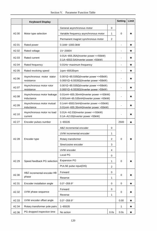
120
Section V. Parameter Function Table
Keyboard Display Setting Limit
A2.00 Motor type selection
General asynchronous motor 0
0 Variable frequency asynchronous motor 1
Permanent magnet synchronous motor 2
A2.01 Rated power 0.1kW~1000.0kW -
A2.02 Rated voltage 1V~2000V -
A2.03 Rated current 0.01A~655.35A(Inverter power <=55kW)
0.1A~6553.5A(Inverter power >55kW) -
A2.04 Rated frequency 0.01Hz~maximum frequency -
A2.05 Rated revolving speed 1rpm~65535rpm -
A2.06 Asynchronous motor stator
resistance
0.001Ω~65.535Ω(Inverter power <=55kW)
0.0001Ω~6.5535Ω(Inverter power >55kW) -
A2.07 Asynchronous motor rotor
resistance
0.001Ω~65.535Ω(Inverter power <=55kW)
0.0001Ω~6.5535Ω(Inverter power >55kW) -
A2.08 Asynchronous motor leakage
inductance
0.01mH~655.35mH(Inverter power <=55kW)
0.001mH~65.535mH(Inverter power >55kW) -
A2.09 Asynchronous motor mutual
inductance
0.1mH~6553.5mH(Inverter power <=55kW)
0.01mH~655.35mH(Inverter power >55kW) -
A2.10 Asynchronous motor no load
current
0.01A~A2.03(Inverter power <=55kW)
0.1A~A2.03(Inverter power >55kW) -
A2.27 Encoder pulses number 1~65535 2500
A2.28 Encoder type
ABZ incremental encoder 0
0
UVW incremental encoder 1
Rotary transformer 2
Sine/cosine encoder 3
UVW encoder 4
A2.29 Speed feedback PG selection
Local PG 0
0 Expansion PG 1
PULSE pulse input(DI5) 2
A2.30 ABZ incremental encoder AB
phase
Forward 0 0
Reserve 1
A2.31 Encoder installation angle 0.0°~359.9° 0 0
A2.32 UVW phase sequence Forward 0
0 Reverse 1
A2.33 UVW encoder offset angle 0.0°~359.9° 0.00
A2.34 Rotary transformer pole pairs 1~65535 1
A2.36 PG dropped inspection time No action 0.0s 0.0s
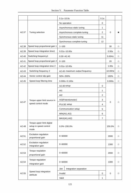
121
Section V. Parameter Function Table
0.1s~10.0s 0.1s
A2.37 Tuning selection
No operation 0
0
Asynchronous static tuning 1
Asynchronous complete tuning 2
Synchronous static tuning 11
Synchronous complete tuning 12
A2.38 Speed loop proportional gain 1 1~100 30
A2.39 Speed loop integration time1 0.01s~10.00s 0.50s
A2.40 Switching frequency1 0.00~A2.43 5.00Hz
A2.41 Speed loop proportional gain 2 0~100 20
A2.42 Speed loop integration time 2 0.01s~10.00s 1.00s
A2.43 Switching frequency 2 A2.40~maximum output frequency 10.00Hz
A2.44 Vector control slip gain 50%~200% 150%
A2.45 Speed-loop filtering time 0.000s~0.100s 0.000s
A2.47 Torque upper limit source in
speed control mode
A2.48 setup 0
0
AI1 1
AI2 2
AI3(Potentiometer) 3
PULSE setup 4
Communication setup 5
MIN(AI1,AI2) 6
MAX(AI1,AI2) 7
A2.48
Torque upper limit digital
setup in speed control
mode
0.0%~200.0% 150.0%
A2.51 Excitation regulation
proportional gain 0~60000 2000
A2.52 Excitation regulation
integration gain 0~60000 1300
A2.53 Torque requlation
proportional gain 0~60000 2000
A2.54 Torque regulation
integration gain 0~60000 1300
A2.55 Speed loop integration
attribute
1bit Integration separation
0 Invalid 0
Valid 1

122
Section V. Parameter Function Table
A2.61 Motor2 control mode
Speed sensorless vector control(SVC) 0
0 Speed sensor vector control(FVC) 1
V/F control 2
A2.62 Motor 2 acc./dec. time
selection
Same with the first motor 0
0
Acceleration time1 1
Acceleration time 2 2
Acceleration time 3 3
Acceleration time 4 4
A2.63 Motor 2 torque hoist
Auto torque hoist 0.0% -
0.1%~30.0%
A2.65 Motor 2 oscillation
suppression gain 0~100 -
5.21 The third motor control: A5.00-A5.09
Code
Description/
Keyboard Display Setting Range
Factory
Setting
Change
Limit
A5.00 DPWM switching frequency
upper limit 0.00Hz~15.00Hz 12.00Hz
A5.00 is only valid for VF control mode. In asynchronous motor VF running mode, square wave
dertermines the continuous modulation mode. Wave value<A5.00:7-stage continuous modulation
mode. Wave value>A5.00:5-stage continuous modulation mode.
In 7-stage continuous modulation mode, inverter switch loss is relatively big, but current ripple is
small. In 5-stage continuous modulation mode, inverter switch loss is relatively small, but current ripple
is big. High frequency may lead to motor operation instability, generally there is no need of modification.
For VF operation instability please refer to P3.11. For inverter loss and temperature rise please
refer to P0.15.
A5.01 PWM modulation mode
Asynchronous modulation 0 0
Synchronous modulation 1
This parameter is only valid for VF control mode. Asynchronous modulation refers to carrier
frequency that linear changes with output frequency, and ensure that the ratio of them (carrier ratio)
remains the same. Generally high output frequency is benefit for output voltage quality.
Generally, synchronous modulation is not needed at low frequencies ( below 100Hz), because the
ratio of carrier frequency and output frequency is relatively high,asynchronous modulation advantage is
more obvious.
When running frequency is greater than 85Hz, synchronous modulation is valid. And fixed as
asynchronous modulation mode when below this frequency.
A5.02 Dead-zone compensation
mode selection
No compensation 0 1
Compensation mode 1 1
Generally speaking , A5.02 needs not to be modified. Only when the output voltage waveform quality
has special requirements or motor appears abnormal phenomenon would users switch the compensation
mode.

123
Section V. Parameter Function Table
A5.03 Random PWM depth
Random PWM invalid 0
0
PWM carrier frequency random depth 1~10
Set the random PWM, monotonous and harsh electromagnetic noise can be changed to the
heterogeneous and soft, the external electromagnetic interference can be effectively reduced. 0
indicates that the PWM is invalid. Different random PWM depth represents different regulation effect.
A5.04 Rapid current-limiting enable Invalid 0
1
Valid 1
Enable the rapid current-limiting function so as to minimize inverter overcurrent protection fault and
make the inverter work normally.
If the inverter long time continuous staying in rapid current-limiting state, it may occur overheating
fault, which is not allowed during operation. Fault alarm of long time rapid current-limiting is 40= Err40 ,
which refers to inverter overload and necessary stop.
A5.05 Current detection
compensation 0~100 5
It is used to set inverter current detection compensation. Excessive setting may lead to decrease of
control performance.Generally do not need to be modified.
A5.06 Under-voltage point setup 60.0%~140.0% 100.0%
A5.06 is used to set value of inverter under-voltage fault 9= E.LU. Different voltage level of 100.0%
corresponds to different voltage point,respectively:
Single phase 220V or three-phase 220V:220V Three-phase 380V:350V
Three phase 480V:450V Three-phase 690V:650V
A5.07 SVC optimization mode
selection
No optimization 0
1 Optimization mode 1 1
Optimization mode 2 2
0:No optimization
1: Optimization mode 1
It is used when there is high torque control linearity requirements.
2: Optimization mode 2
It is used when there is high speed stability requirement.
A5.08 Dead zone time adjustment 100%~200% 150%
This parameter is set according to 1140V voltage level. By adjusting the value can improve the
voltage effective use rate. Users are not suggested to modify.
A5.09 Overvoltage point setup 200.0V~2500.0V 810.0V
A5.09 is overvoltage point set through software, which is not related to hardware overvoltage point.
5.22 AI curve setup: A6.00-A6.29
Code Description/
Keyboard Display Setting Range
Factory
Setting
Change
Limit
A6.00 AI curve 4 minimum input -10.00V~A6.02 0.00V
A6.01 AI curve 4 minimum input
corresponding setup -100.0%~100.0% 0.0%
A6.02 AI curve 4inflection point 1 A6.00~A6.04 3.00V
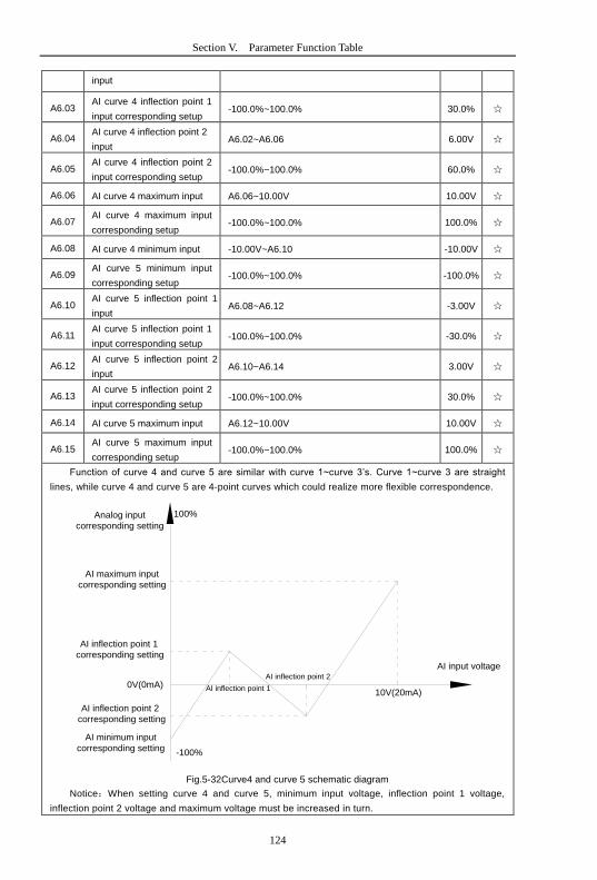
124
Section V. Parameter Function Table
input
A6.03 AI curve 4 inflection point 1
input corresponding setup -100.0%~100.0% 30.0%
A6.04 AI curve 4 inflection point 2
input A6.02~A6.06 6.00V
A6.05 AI curve 4 inflection point 2
input corresponding setup -100.0%~100.0% 60.0%
A6.06 AI curve 4 maximum input A6.06~10.00V 10.00V
A6.07 AI curve 4 maximum input
corresponding setup -100.0%~100.0% 100.0%
A6.08 AI curve 4 minimum input -10.00V~A6.10 -10.00V
A6.09 AI curve 5 minimum input
corresponding setup -100.0%~100.0% -100.0%
A6.10 AI curve 5 inflection point 1
input A6.08~A6.12 -3.00V
A6.11 AI curve 5 inflection point 1
input corresponding setup -100.0%~100.0% -30.0%
A6.12 AI curve 5 inflection point 2
input A6.10~A6.14 3.00V
A6.13 AI curve 5 inflection point 2
input corresponding setup -100.0%~100.0% 30.0%
A6.14 AI curve 5 maximum input A6.12~10.00V 10.00V
A6.15 AI curve 5 maximum input
corresponding setup -100.0%~100.0% 100.0%
Function of curve 4 and curve 5 are similar with curve 1~curve 3’s. Curve 1~curve 3 are straight
lines, while curve 4 and curve 5 are 4-point curves which could realize more flexible correspondence.
Fig.5-32Curve4 and curve 5 schematic diagram
Notice:When setting curve 4 and curve 5, minimum input voltage, inflection point 1 voltage,
inflection point 2 voltage and maximum voltage must be increased in turn.
100%Analog input
corresponding setting
AI maximum input
corresponding setting
AI inflection point 1
corresponding setting
0V(0mA)
AI inflection point 2
corresponding setting
AI minimum input
corresponding setting
AI inflection point 1
10V(20mA)
AI input voltage
-100%
AI inflection point 2

125
Section V. Parameter Function Table
A6.24 AI1 set hopping point -100.0%~100.0% 0.0%
A6.25 AI1 set hopping amplitude 0.0%~100.0% 0.5%
A6.26 AI2 set hopping point -100.0%~100.0% 0.0%
A6.27 AI2 set hopping amplitude 0.0%~100.0% 0.5%
A6.28 AI3 set hopping point -100.0%~100.0% 0.0%
A6.29 AI3 set hopping amplitude 0.0%~100.0% 0.5%
Analog input AI1~AI3 of HV590 are all provided with hopping function for set value.
Hopping frequency refers to fixing of analog corresponding setup to the value of hopping point
when analog correspondending setting varies within jump point upper/lower limit.
E.g:
Voltage of analog input AI1 is in 5.00V fluctuation, which range is 4.90V~5.10V. Minimum input
0.00V corresponding to 0.0%, while maximum input 10.00V corresponding to 100.%.The corresponding
setting of AI1 fluctuates between 49.0%~51.0%.
Set A5.16 to 50.0% and A5.17 to 1.0%, after hopping function processing, AI1 is fixed as 50.0%. In
this way, AI1 is converted into a stable input, and fluctuation is eliminated.
5.23 User programmable card parameters: A7.00-A7.09
Code Description/
Keyboard Display Setting Range
Factory
Setting
Change
Limit
A7.00 User programmable function
selection
Invalid 0 0
Valid 1
A7.01 Control board output terminal
control mode selection
Inverter control 0
-
User programmable card control 1
1bit Y1P(Y1 as pulse output)
10bit Relay(T/A1-T/B1-T/C1)
100
bit DO1
1000
bit Y1R(Y1 as switch output)
10000
bit AO1
A7.02 Programmable card expansion
AI3x function configuration
See《User programmable control card》 for
supplementary description -
A7.03 Y1P output 0.0%-100.0% 0.0%
A7.04 AO1 output 0.0%-100.0% 0.0%
A7.05 Switch output
1bit Y1R
000 10bit Relay 1
100
bit DO
A7.06 Programmable card
frequency setup 0.0%-100.0% 0.0%
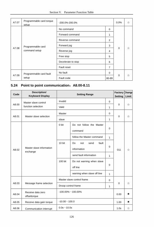
126
Section V. Parameter Function Table
A7.07 Programmable card torque
setup -200.0%-200.0% 0.0%
A7.08 Programmable card
command setup
No command 0
0
Forward command 1
Reverse command 2
Forward jog 3
Reverse jog 4
Free stop 5
Decelerate to stop 6
Fault reset 7
A7.09 Programmable card fault
setup
No fault 0 0
Fault code 80-89
5.24 Point to point communication:A8.00-8.11
Code Description/
Keyboard Display Setting Range
Factory
Setting
Change
Limit
A8.00 Master slave control
function selection
Invalid 0
0 Valid 1
A8.01 Master slave selection Master 0
0
slave 1
A8.02 Master slave information
exchange
0 bit Do not follow the Master
command 0
011
follow the Master command 1
10 bit Do not send fault
information 0
send fault information 1
100 bit Do not warning when slave
off line 0
warning when slave off line 1
A8.03 Message frame selection
Master slave control frame 0
0 Droop control frame 1
A8.04 Receive data zero
offsettorque
-100.00%~100.00% 0.00
A8.05 Receive data gain torque -10.00~100.0 1.00
A8.06 Communication interrupt 0.0s~10.0s 1.0s
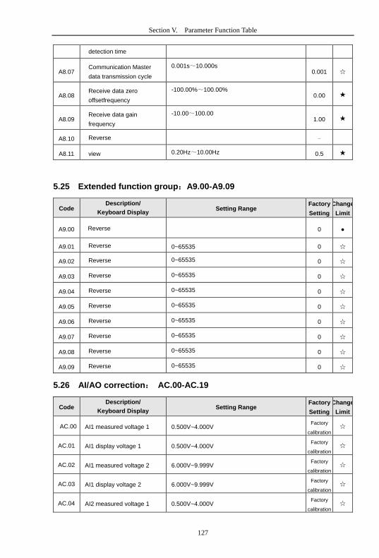
127
Section V. Parameter Function Table
detection time
A8.07 Communication Master
data transmission cycle
0.001s~10.000s 0.001
A8.08 Receive data zero
offsetfrequency
-100.00%~100.00% 0.00
A8.09 Receive data gain
frequency
-10.00~100.00 1.00
A8.10 Reverse -
A8.11 view 0.20Hz~10.00Hz 0.5
5.25 Extended function group:A9.00-A9.09
Code Description/
Keyboard Display Setting Range
Factory
Setting
Change
Limit
A9.00 Reverse 0
A9.01 Reverse 0~65535 0
A9.02 Reverse 0~65535 0
A9.03 Reverse 0~65535 0
A9.04 Reverse 0~65535 0
A9.05 Reverse 0~65535 0
A9.06 Reverse 0~65535 0
A9.07 Reverse 0~65535 0
A9.08 Reverse 0~65535 0
A9.09 Reverse 0~65535 0
5.26 AI/AO correction: AC.00-AC.19
Code Description/
Keyboard Display Setting Range
Factory
Setting
Change
Limit
AC.00 AI1 measured voltage 1 0.500V~4.000V Factory
calibration
AC.01 AI1 display voltage 1 0.500V~4.000V Factory
calibration
AC.02 AI1 measured voltage 2 6.000V~9.999V Factory
calibration
AC.03 AI1 display voltage 2 6.000V~9.999V Factory
calibration
AC.04 AI2 measured voltage 1 0.500V~4.000V Factory
calibration

128
Section V. Parameter Function Table
AC.05 AI2 display voltage 1 0.500V~4.000V Factory
calibration
AC.06 AI2 measured voltage 2 6.000V~9.999V Factory
calibration
AC.07 AI2 display voltage 2 6.000V~9.999V Factory
calibration
AC.08 AI3 measured voltage 1 -9.999V~10.000V Factory
calibration
AC.09 AI3 display voltage 1 -9.999V~10.000V Factory
calibration
AC.10 AI3 measured voltage 2 -9.999V~10.000V Factory
calibration
AC.11 AI3 display voltage 2 -9.999V~10.000V Factory
calibration
This group of function codes are used for calibration of analog input AI , which could eliminate AI
input bias and gain influence. Generally , there is no need of calibration in application, for it has been
calibrated in factory. When restoring the factory value, the parameter would be restored to the default
value of factory calibration.
Measured voltage refers to the actual voltage that has been measured through measuring
instrument such as multimeter. Display voltage refers to the display value that has been sampled by the
inverter. See U0 group (U0.21、U0.22、U0.23) display.
During calibration, put the multimeter measurement value and the U0 value respectively into the
function codes above, inverter would automatically calibrate the AI zero off and gain.
AC.12 A01 target voltage 1 0.500V~4.000V Factory
calibration
AC.13 A01 measured voltage 1 0.500V~4.000V Factory
calibration
AC.14 A01 target voltage 2 6.000V~9.999V Factory
calibration
AC.15 A01 measured voltage 2 6.000V~9.999V Factory
calibration
AC.16 A02 target voltage 1 0.500V~4.000V Factory
calibration
AC.17 A02 measured voltage 1 0.500V~4.000V Factory
calibration
AC.18 A02 target voltage 2 6.000V~9.999V Factory
calibration
AC.19 A02 measured voltage 2 6.000V~9.999V Factory
calibration
This group of function codes are used for calibration of analog output AO. Generally , there is no
need of calibration in application, for it has been calibrated in factory. When restoring the factory value,
the parameter would be auto restored to the default value of factory calibration.
Target voltage refers to inverter theoretical output voltage, while measured voltage refers to the
actual voltage that has been measured through measuring instrument such as multimeter.

129
Section VI. Fault Diagnosis & Solutions
Section VI. Fault Diagnosis & Solutions
HV590 is able to make full use of the device performance, while implementing effective
protection. You may encounter following fault tips during operation, please control the following
table analysis the possible causes, and rule out the fault.
6.1 Fault alarm and solutions
HV590 series can not only make full use of equipment performance but also implement
effective protection. HV590 series has 51 alarming information and protection function.Once
fault occurs, protection function acts,output stops, inverter fault relay contact starts,and fault
code is been displayed on the display panel. Before consulting the service department, the user
can perform self-check according to the prompts of this chapter, analyze the fault cause and find
out t solution. If the fault is caused by the reasons as described in the dotted frame, please
consult the agents or our company directly.
Among the 51 items of warning information:
Fault no.22= Err22refers to hardware over-current or over-voltage signal.In most cases
hardware over-voltage fault led to fault no.22= Err22 alarming.
Fault name Inverter unit protection
Panel display Fault No.1= Err01
Fault investigation
1、Inverter output loop short circuit
2、Two long wiring between motor and inverter.
3、Module overheating
4、Inverter internal wiring loose
5、Main control board anomalies
6、Drive board anomalies
7、Inverter module anomalies
Fault
countermeasures
1、Eliminate external faults
2、Add reactor or output filter
3、Check air duct, fan and eliminate existing problems.
4、Insert all connecting wires
5、For technical support
Fault name Acceleration over current
Panel display Fault No.2= Err02
Fault investigation
1、Acceleration time too short
2、Improper manual torque boost or V/F curve
3、Low voltage
4、Inverter output loop grouded or short circuit
5、Vector control mode without parameter identification
6、Start the rotating motor
7、Sudden load add in acceleration process
8、Small type selection of inverter.
Fault 1、Increase acceleration time

130
Section VI. Fault Diagnosis & Solutions
countermeasures 2、Adjust manual torque boost or V/F curve
3、Adjust voltage to normal range
4、Eliminate external faults
5、Parameter identification
6、Select speed tracking start or restart after motor stop
7、Cancel sudden added load
8、Choose inverter of greater power level
Fault name Deceleration over current
Panel display Fault No.3= Err03
Fault investigation
1、Inverter output loop grouded or short circuit
2、Vector control mode without parameter identification
3、Deceleration time too short
4、Low voltage
5、Sudden load add in deceleration process
6、No braking unit and brake resistence installed
Fault
countermeasures
1、Eliminate external faults
2、Parameter identification
3、Increase deceleration time
4、Adjust voltage to normal range
5、Cancel sudden added load
6、Install braking unit and brake resistence
Fault name Constant speed over current
Panel display Fault No.4= Err04
Fault investigation
1、Inverter output loop grouded or short circuit
2、Vector control mode without parameter identification
3、Low voltage
4、Sudden load add in deceleration process
5、Small type selection of inverter
Fault
countermeasures
1、Eliminate external faults
2、Parameter identification
3、Adjust voltage to normal range
4、Cancel sudden added load
5、Choose inverter of greater power level
Fault name Acceleration over voltage
Panel display Fault No.5= Err05
Fault investigation
1、No braking unit and brake resistence installed
2、High input voltage
3、External force drive motor operation during acceleration process
4、Acceleration time too short
Fault
countermeasures
1、Install braking unit and brake resistence
2、Adjust voltage to normal range
3、Cancel external force or install brake resistence
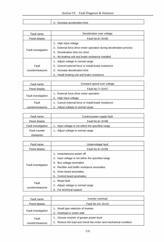
131
Section VI. Fault Diagnosis & Solutions
4、Increase acceleration time
Fault name Deceleration over voltage
Panel display Fault No.6= Err06
Fault investigation
1、High input voltage
2、External force drive motor operation during deceleration process
3、Deceleration time too short
4、No braking unit and brake resistence installed
Fault
countermeasures
1、Adjust voltage to normal range
2、Cancel external force or install brake resistence
3、Increase deceleration time
4、Install braking unit and brake resistence
Fault name Constant speed over voltage
Panel display Fault No.7= Err07
Fault investigation 1、External force drive motor operation
2、High input voltage
Fault
countermeasures
1、Cancel external force or install brake resistence
2、Adjust voltage to normal range
Fault name Control power supply fault
Panel display Fault No.8= Err08
Fault investigation 1、Input voltage is not within the specified range
Fault counter
measures
1、Adjust voltage to normal range
Fault name Undervoltage fault
Panel display Fault No.9= Err09
Fault investigation
1、Instantaneous power-off
2、Input voltage is not within the specified range
3、Bus voltage anomalies
4、Rectifier and buffer resistance anomalies
5、Drive board anomalies
6、Control board anomalies
Fault
countermeasures
1、Reset fault
2、Adjust voltage to normal range
3、For technical support
Fault name Inverter overload
Panel display Fault No.10= Err10
Fault investigation 1、Small type selection of inverter.
2、Overload or motor stall
Fault
countermeasures
1、Choose inverter of greater power level
2、Reduce the load and check the motor and mechanical condition

132
Section VI. Fault Diagnosis & Solutions
Fault name Motor overload
Panel display Fault No.11= Err11
Fault investigation
1、Small type selection of inverter
2、Improper setup of P9.01
3、Overload or motor stall
Fault counter
measures
1、Choose inverter of greater power level
2、Set P9.01 correctly
3、Reduce the load and check the motor and mechanical condition
Fault name Input phase lack
Panel display Fault No.12= Err12
Fault investigation
1、Drive board anomalies
2、Lightning protection board (BESP ) anomalies
3、Control board anomalies
4、3-phase input power-supply anomalies
Fault
countermeasures
1、Replace driver, power- supply board or contactor
2、For technical support
3、Eliminate external loop faults
Fault name Output phase lack
Panel display Fault No.13= Err13
Fault investigation
1、Wiring between motor and inverter anomalies
2、Inverter unbalanced 3-phase output
3、Drive board anomalies
4、Module anomalies
Fault counter
measures
1、Eliminate external loop faults
2、Check 3-phase winding and eliminate faults
3、For technical support
Fault name Module overheating
Panel display Fault No.14= Err14
Fault investigation
1、Air duct block
2、Fan damage
3、High ambient temperature
4、Module thermistor damage
5、Inverter module damage
Fault counter
measures
1、Clean air dust
2、Replace the fan
3、Reduce ambient temperature
4、Replace thermistor
5、Replace inverter module
Fault name External equipment fault
Panel display Fault No.15= Err15

133
Section VI. Fault Diagnosis & Solutions
Fault investigation 1、Input external fault signal through DI
2、Input external fault signal through IO
Fault counter
measures 1、Reset operation
Fault name Communication fault
Panel display Fault No.16= Err16
Fault investigation
1、Abnornal communication cable
2、Wrongly set communication expansion card P0.28
3、Wrongly set communication parameter PD group
4、Position machine operation anomalies
Fault counter
measures
1、Check the communication cable
2、Set communication expansion card type correctly
3、Set communication parameter correctly
4、Check position machine cable
Fault name Contactor fault
Panel display Fault No.17= Err17
Fault investigation 1、Input phase lack
2、Drive board , contactor anomalies
Fault counter
measures
1、Eliminate external loop faults
2、Replace driver, power- supply board or contactor
Fault name Current inspection fault
Panel display Fault No.18= Err18
Fault investigation 1、Drive board anomalies
2、Hall devices anomalies
Fault counter
measures
1、Replace drive board
2、Replace hall devices
Fault name Motor tuning fault
Panel display Fault No.19= Err19
Fault investigation 1、Parameter identification process overtime
2、Wrongly set motor parameters
Fault counter
measures
1、Check wire between inverter and motor
2、Set motor parameters correctly according to the nameplate
Fault name Encoder /PG card fault
Panel display Fault No.20= Err20
Fault investigation
1、Encoder anomalies
2、PG card anomalies
3、Encoder type mismatch
4、Encoder connections fault
Fault counter
measures
1、Replace encoder
2、Replace PG card
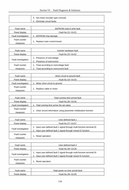
134
Section VI. Fault Diagnosis & Solutions
3、Set motor encoder type correctly
4、Eliminate circuit faults
Fault name EEPROM read & write fault
Panel display Fault No.21= Err21
Fault investigation 1、EEPROM chip damage
Fault counter
measures 1、Replace main control board
Fault name Inverter hardware fault
Panel display Fault No.22= Err22
Fault investigation 1、Presence of overvoltage
2、Presence of overcurrent
Fault counter
measures
1、Treat according to overvoltage fault
2、Treat according to overcurrent fault
Fault name Short circuit to ground fault
Panel display Fault No.23= Err23
Fault investigation 1、Motor short circuit to ground
Fault counter
measures 1、Replace cable or motor
Fault name Total running time arrival fault
Panel display Fault No.26= Err26
Fault investigation 1、Total running time arrive the set value
Fault counter
measures 1、Clear record information using parameter initialization function
Fault name User-defined fault 1
Panel display Fault No.27= Err27
Fault investigation 1、Input user-defined fault 1 signal through multi-function terminal DI
2、Input user-defined fault 1 signal through virtual IO function
Fault counter
measures 1、Reset operation
Fault name User-defined fault 2
Panel display Fault No.28= Err28
Fault investigation 1、Input user-defined fault 2 signal through multi-function terminal DI
2、Input user-defined fault 2 signal through virtual IO function
Fault counter
measures 1、Reset operation
Fault name Total power-on time arrival fault
Panel display Fault No.29= Err29
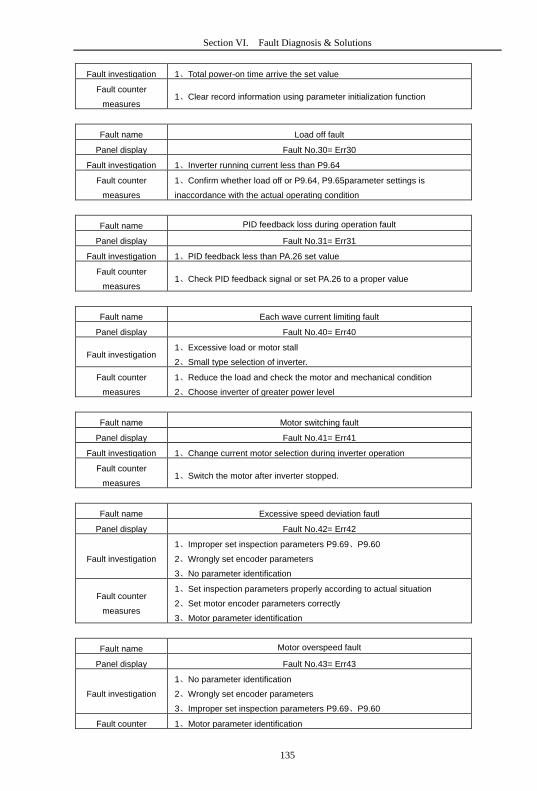
135
Section VI. Fault Diagnosis & Solutions
Fault investigation 1、Total power-on time arrive the set value
Fault counter
measures 1、Clear record information using parameter initialization function
Fault name Load off fault
Panel display Fault No.30= Err30
Fault investigation 1、Inverter running current less than P9.64
Fault counter
measures
1、Confirm whether load off or P9.64, P9.65parameter settings is
inaccordance with the actual operating condition
Fault name PID feedback loss during operation fault
Panel display Fault No.31= Err31
Fault investigation 1、PID feedback less than PA.26 set value
Fault counter
measures 1、Check PID feedback signal or set PA.26 to a proper value
Fault name Each wave current limiting fault
Panel display Fault No.40= Err40
Fault investigation 1、Excessive load or motor stall
2、Small type selection of inverter.
Fault counter
measures
1、Reduce the load and check the motor and mechanical condition
2、Choose inverter of greater power level
Fault name Motor switching fault
Panel display Fault No.41= Err41
Fault investigation 1、Change current motor selection during inverter operation
Fault counter
measures 1、Switch the motor after inverter stopped.
Fault name Excessive speed deviation fautl
Panel display Fault No.42= Err42
Fault investigation
1、Improper set inspection parameters P9.69、P9.60
2、Wrongly set encoder parameters
3、No parameter identification
Fault counter
measures
1、Set inspection parameters properly according to actual situation
2、Set motor encoder parameters correctly
3、Motor parameter identification
Fault name Motor overspeed fault
Panel display Fault No.43= Err43
Fault investigation
1、No parameter identification
2、Wrongly set encoder parameters
3、Improper set inspection parameters P9.69、P9.60
Fault counter 1、Motor parameter identification
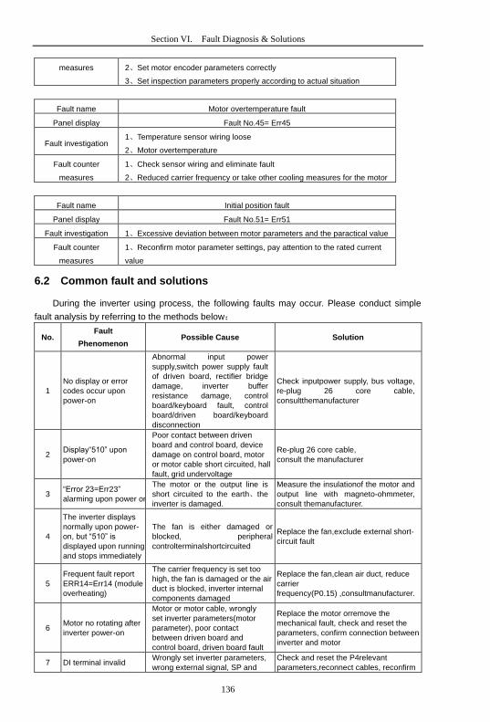
136
Section VI. Fault Diagnosis & Solutions
measures 2、Set motor encoder parameters correctly
3、Set inspection parameters properly according to actual situation
Fault name Motor overtemperature fault
Panel display Fault No.45= Err45
Fault investigation 1、Temperature sensor wiring loose
2、Motor overtemperature
Fault counter
measures
1、Check sensor wiring and eliminate fault
2、Reduced carrier frequency or take other cooling measures for the motor
Fault name Initial position fault
Panel display Fault No.51= Err51
Fault investigation 1、Excessive deviation between motor parameters and the paractical value
Fault counter
measures
1、Reconfirm motor parameter settings, pay attention to the rated current
value
6.2 Common fault and solutions
During the inverter using process, the following faults may occur. Please conduct simple
fault analysis by referring to the methods below:
No. Fault
Phenomenon Possible Cause Solution
1
No display or error
codes occur upon
power-on
Abnormal input power
supply,switch power supply fault
of driven board, rectifier bridge
damage, inverter buffer
resistance damage, control
board/keyboard fault, control
board/driven board/keyboard
disconnection
Check inputpower supply, bus voltage,
re-plug 26 core cable,
consultthemanufacturer
2 Display“510” upon
power-on
Poor contact between driven
board and control board, device
damage on control board, motor
or motor cable short circuited, hall
fault, grid undervoltage
Re-plug 26 core cable,
consult the manufacturer
3 “Error 23=Err23”
alarming upon power on
The motor or the output line is
short circuited to the earth、the
inverter is damaged.
Measure the insulationof the motor and
output line with magneto-ohmmeter,
consult themanufacturer.
4
The inverter displays
normally upon power-
on, but “510” is
displayed upon running
and stops immediately
The fan is either damaged or
blocked, peripheral
controlterminalshortcircuited
Replace the fan,exclude external short-
circuit fault
5
Frequent fault report
ERR14=Err14 (module
overheating)
The carrier frequency is set too
high, the fan is damaged or the air
duct is blocked, inverter internal
components damaged
Replace the fan,clean air duct, reduce
carrier
frequency(P0.15) ,consultmanufacturer.
6 Motor no rotating after
inverter power-on
Motor or motor cable, wrongly
set inverter parameters(motor
parameter), poor contact
between driven board and
control board, driven board fault
Replace the motor orremove the
mechanical fault, check and reset the
parameters, confirm connection between
inverter and motor
7 DI terminal invalid Wrongly set inverter parameters,
wrong external signal, SP and
Check and reset the P4relevant
parameters,reconnect cables, reconfirm
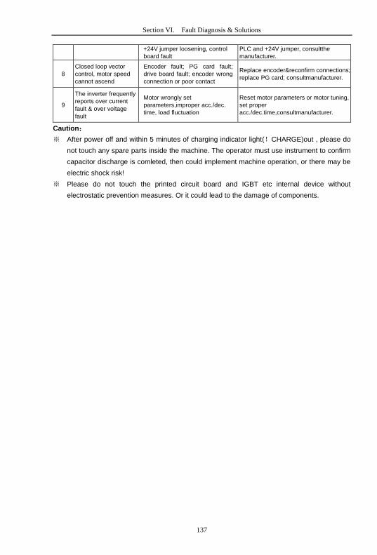
137
Section VI. Fault Diagnosis & Solutions
+24V jumper loosening, control
board fault
PLC and +24V jumper, consultthe
manufacturer.
8
Closed loop vector
control, motor speed
cannot ascend
Encoder fault; PG card fault;
drive board fault; encoder wrong
connection or poor contact
Replace encoder&reconfirm connections;
replace PG card; consultmanufacturer.
9
The inverter frequently
reports over current
fault & over voltage
fault
Motor wrongly set
parameters,improper acc./dec.
time, load fluctuation
Reset motor parameters or motor tuning,
set proper
acc./dec.time,consultmanufacturer.
Caution:
※ After power off and within 5 minutes of charging indicator light(!CHARGE)out , please do
not touch any spare parts inside the machine. The operator must use instrument to confirm
capacitor discharge is comleted, then could implement machine operation, or there may be
electric shock risk!
※ Please do not touch the printed circuit board and IGBT etc internal device without
electrostatic prevention measures. Or it could lead to the damage of components.

147
Section VII. Inspection & Maintenance
7.1 Inspection and Maintenance
Under normal working conditions, in addition to daily inspection, the frequency converter
should be subject to regular inspection (for example inspection for overhaul or as specified but
at an interval of at most six months). Please refer to the following table in order to prevent faults.
Daily Regular Check item Check details Method Criterion
√ LED display If any abnormal display Visual check As per use state
√ √ Fan If any abnormal noise or
vibration Visual and audible check No anomalies
√ Surrounding
conditions
Temperature, humidity, dust
content, harmful gas, etc.
Visual\audible\sensory
check As per 2-1 item
√
Input output
voltage
If any abnormal input, output
voltage
Measure R, S, T and
U, V, W terminals
As per standard
specifications
√ Main circuit
Fasteners whether loose, if
any signs showing overheat,
discharging, or too high dust
content, or the air piping is
blocked
Check visually, tighten
the fastenings, and clean
the related parts
No anomalies
√
Electrolytic
capacitor If any abnormal appearance Check visually No anomalies
√ Current-conducting
leads or blocks Loose or not Check visually No anomalies
√
Terminals If the screws or bolts loose Tighten the loose
screws or bolts No anomalies
“√” means need daily check or regularly check.
For inspection,do not disassemble or shake the parts without reason, or pull off the plug-in-
parts at random. Otherwise, the unit will not operate normally, or can not enter the mode of fault
display, or causes faults of components or even parts of the main switch components IGBT
module is damaged.
When needing measurement, the user should note that much different results will be gained
possibly if the measuring is performed with different instruments. It is recommended that the
input voltage be measured with pointer-type voltmeter, output voltage with rectification voltmeter,
input and output current with tong-test ammeter, and power with electrically-driven wattmeter.

148
Section VII. Inspection & Maintenance
7.2 Regular replacement of the device
In order to ensure the operation reliability of the frequency converter, in addition to regular
maintenance and inspection, all the parts suffering long-term mechanical wear should be
replaced at a regular interval, which includes all cooling fans and the filtering capacitors of main
circuits for energy buffer and interchange and PCBs. For continuous use under normal
conditions, these parts can be replaced according to the following table and the operating
environment, loads and the current state of frequency converter.
Part name Standard replacement years
Cooling fan 1~3 years
Filtering capacitor 4~5 years
PCB
(printed circuit board) 5~8 years
7.3 Storage
The following actions must be taken if the frequency converter is not put into use
immediately after delivery to the user and need to keep well for the time being or stored for a
long time:
※ Stored in a dry and adequately-ventilated place without dust and metal powder at the
temperature specified in the specifications.
※ If the frequency converter is not put into use after one year, a charge test should be made,
so as to resume the performance of the filtering capacitor of main circuit in it. For charging,
a voltage regulator should be used to slowly increase the input voltage of the frequency
converter until it reaches the rating, and the charge should last more than 1~2 hours. This
test should be made at least once a year.
※ Don’t perform breakdown test at random, for this test will cause shorter life of the frequency
converter. The insulation test must be performed after the insulation resistance is measured
with a 500-volt mega ohm and this value must not be less than 4MΩ.
7.4 Measuring and Judgment
※ If the current is measured with the general instrument, imbalance will exists for the current
at the input terminal. Generally, differing by not more than 10% is normal. If it differs by 30%,
inform the factory to replace the rectification bridge, or check if the error of three-phase
input voltage is above 5V.
※ If the three-phase output voltage is measured with a general multi-meter, the read data is
not accurate due to the interference of carrier frequency and only for reference.
7.5 Safety Precaution
※ Only specially trained persons are allowed to disassembly,replace the drive components.
※ Before the inspection and maintenance,inverter must be confirmed at least 5 minutes after
power off or charged(CHARGE) light is off,otherwise there is risk of electric shock.
※ Avoid metal parts leaving in the drive, or it may result in equipment damage.

149
Appendix I H5RS485 Card & RS485Communication Protocol
I.1 H5RS485 card
H5RS485 card produced by HNC is used with HV590 series inverter as RS485
communication card. It contains the following resources:
Table 2Jumper description
Jumper number Description
J1 SP1 connection mode selection
J2 RS485 Termination resistor selection
I.2 Communication protocol
I.2.1 Protocol content
The serial communication protocol defines the information content and format of the
use of the transmission in serial communication. Including: the host polling (or broadcast)
format、host encoding methods.Concent including: require action of the function code,
data transmission and error checking and so on. Slave machine's response is the same
structure, including: action confirmation, return data and error checking. Slave error
occurred when receiving information, or can not do what the host request action, it will
organize a fault messageas the response back to the host computer.
Application mode:
The inverter accessing with “ single main multi-slave” PC/PLC control network which
equipped with RS232/RS485 bus.
Bus structure:
(1) Interface mode
RS232/RS485 hardware interface
(2) Transmission mode
Asynchronous serial, half-duplex transmission. At the same time host and slave
computer can only permit one to send data while the other can only receive data. Data in
the process of serial asynchronous communication is in the message format and sent one
frame by one frame.
(3) Topological mode
In single-master system, the setup range of slave address is 1 to 247. Zero refers to
broadcast communication address. The address of slave must is exclusive in the network.
That is one condition of one slave machine.
I.3 Protocol Description
HV590 series inverter communication protocol is an asynchronous serial master-slave
Modbus communication protocol, only one device in the network (master) to establish
protocol (known as the "query / command"). Other device (slave) can only provide data
response to the host query / command, or make the appropriate action according to the
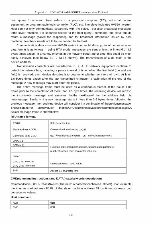
150
Appendix I H5RS485 Card & RS485Communication Protocol
host query / command. Host refers to a personal computer (PC), industrial control
equipment, or programmable logic controller (PLC), etc. The slave indicates HV590 inverter.
Host can not only communicate separately with the slave, but also broadcast messages
tothe lower machine. For separate access to the host query / command, the slave should
return a message (called the response), and for broadcast information issued by host
machine , feedback needs not to be responded to the host.
Communication data structure HV590 series inverter Modbus protocol communication
data format is as follows: using RTU mode, messages are sent at least at interval of 3.5
bytes times pause. In a variety of bytes in the network baud rate of time, this could be most
easily achieved (see below T1-T2-T3-T4 shown). The transmission of a do main is the
device address.
Transmission characters are hexadecimal 0...9, A...F. Network equipment continue to
detect the network bus, including a pause interval of time. When the first field (the address
field) is received, each device decodes it to determine whether sent to their own. At least
3.5 bytes times pause after the last transmitted character, a calibration of the end of the
message. A new message may start after this pause.
The entire message frame must be used as a continuous stream. If the pause time
frame prior to the completion of more than 1.5 byte times, the receiving device will refresh
the incomplete message and assumes thatthe nextbytewill be the address field ofa
newmessage. Similarly, if a new message starts in less than 3.5 bytes times following the
previous message, the receiving device will consider it a continuationof thepreviousmessage.
Thiswillsetanerror, asthevaluein thefinalCRCfieldwillnotbevalidforthecombinedmessages.A
typical message frame is shownbelow.
RTU frame format:
START 3.5-character time
Slave address ADDR Communication address:1~247
Command code CMD 03:Read slaveparameters;06:Writeslaveparameters
DATA(N-1)
Function code parameter address,function code parameter
number,function code parameter value,etc.
DATA(N-2)
………………………
DATA0
CRC CHK loworder Detection value:CRC value。
CRC CHK highorder
END Atleast 3.5-character time
CMD(command instructions) and DATA(material words description)
Commandcode:03H,readsNwords(Thereare12characterscanberead atmost). For example:
the inverter start address F0.02 of the slave machine address 01 continuously reads two
consecutive values.
Host command
ADR 01H
CMD 03H

151
Appendix I H5RS485 Card & RS485Communication Protocol
Start address highorder F0H
Start address loworder 02H
Register number highorder 00H
Register number loworder 02H
CRC CHK low order CRC CHK values to be calculated
CRC CHK high order
Slave response
PD.05=0:
ADR 01H
CMD 03H
Byte number high order 00H
Byte number low order 04H
Data P002H high order 00H
Data P002H low order 00H
Data P003H high order 01H
CRC CHK low order CRC CHK values to be calculated
CRC CHK high order
PD.05=1:
ADR 01H
CMD 03H
Byte number 04H
Data F002H high order 00H
Data F002H low order 00H
Data F003H high order 00H
Data F003H low order 01H
CRC CHK low order CRC CHK values to be calculated
CRC CHK high order
Command code:06H write a word
For example: Write 5000(1388H) into F00AH which slave address is 02H.
Master command information
ADR 02H
CMD 06H
Data address high order F0H
Data address low order 0AH
Data content high order 13H
Data content low order 88H
CRC CHK low order CRC CHK values to be calculated
CRC CHK high order

152
Appendix I H5RS485 Card & RS485Communication Protocol
Slave response
ADR 02H
CMD 06H
Data address high order F0H
Data address low order 0AH
Data content high order 13H
Data content low order 88H
CRC CHK low order CRC CHK values to be calculated
CRC CHK high order
I.4 Cyclical Redundancy Check
Cyclical Redundancy Check—CRC mode:CRC(Cyclical Redundancy Check) is in RTU
frame format, message contains an error-checking field that is based on a CRC method. The
CRC field checks the contents of the entire message. The CRC field is two bytes, containing a
16-bit binary value. The CRC value is calculated by the transmitting device, which appends the
CRC to the message. The receiving device recalculates a CRC during receipt of the message,
and compares the calculated value to the actual value it received in the CRC field. If the two
values are not equal, an error results. The CRC is started by 0xFFFF. Then a process begins of
applying successive 8-bit bytes of the message to the current contents of the register. Only the
eight bits of data in each character are used for generating the CRC. Start and stop bits, and the
parity bit, do not apply to the CRC.
During generation of the CRC, each eight-bit character is exclusive XOR with the register
contents. Then the result is shifted in the direction of the least significant bit (LSB), with a ZERO
filled into the most significant bit (MSB) position. The LSB extracted and examined. If the LSB
was 1, the register then exclusive XOR with a preset, fixed value. If the LSB was 0, no exclusive
XOR takes place. This process is repeated until 8 shifts have been performed. After the last (8)
shift, the next eight-bit byte is exclusive XOR with the register’s current value, and the process
repeats for 8 more shifts as described above. The final contents of the register, after all the
bytes of the message have been applied, is the CRC value.
When CRC appended to the message, the low byte is appended first, and then the high
byte.
CRC calculation program:
unsigned int cal_crc16 (unsigned char *data, unsigned int length)
unsigned int i,crc_result=0xffff;
while(length--)
crc_result^=*data++;
for(i=0;i<8;i++)
if(crc_result&0x01)

153
Appendix I H5RS485 Card & RS485Communication Protocol
crc_result=(crc_result>>1)^0xa001;
else
crc_result=crc_result>>1;
crc_result=((crc_result&0xff)<<8)|(crc_result>>8);
return(crc_result);

154
Appendix I H5RS485 Card & RS485Communication Protocol
I.5 Communication parameter address
The chapter is about communication contents, it’s used to control the inverter operation, the
status of the inverter and related parameter setup. Read and write functioncode parameters
(Some function codesare not able to be changed, only for the manufacturer use.). The mark
rules of function code parameters address:
The group number and mark of function codesare parameter address for indication rules.
High byte:F0~FF(P group), A0~AF(A group), 70~F(U group)Low byte:00~FF
For example: P3.12, the address indicates F30C
Caution:
Group PF: Parameters could not be read or be modified.
Group U: Parameters could be read but not be modified.
Some parameters can not be changed during operation, some parameters regardless of
the kind of state the inverter in, the parameters can not be changed. Change the function code
parameters, pay attention to the scope of the parameters, units, and relative instructions.
Besides, if EEPROM is frequently stored, it will reduce the service life of EEPROM. In some
communication mode, function code need to be stored as long as changing the RAM value.
Group P: to achieve this function, change high order F of the function code address into 0.
Group A: to achieve this function, change high order A of the function code address to be 4.
Corresponding function code address are indicated below:
High byte: 00~0F(P group), 40~4F(A group)Low byte: 00~FF
For example:
Function code P3.12 can not be stored into EEPROM, address indicates to be
030C,function code A0-05 can not be stored in EEPROM, address indicates to be 4005;This
address can only act writing RAM, it can not act reading, when act reading, it is invalid address.
For all parameters, command code 07H can be used to achieve this function.
Stop/running parameter:
Parameter addr. Parameter description
1000 * Communication setup value(-10000~10000)(Decimal)
1001 Running frequency
1002 Bus voltage
1003 Output voltage
1004 Output current
1005 Output power
1006 Output torque
1007 Running speed
1008 DI input status
1009 DO output status
100A AI1voltage
100B AI2 voltage

155
Appendix I H5RS485 Card & RS485Communication Protocol
100C AI3 voltage
100D Counting value input
100E Length value input
100F Load speed
1010 PID setup
1011 PID feedback
1012 PLC process
1013 PULSE input pulse frequency, unit 0.01kHz
1014 Feedback speed, unit 0.1Hz
1015 Rest running time
1016 AI1 voltage before correction
1017 AI2 voltage before correction
1018 AI3 voltage before correction
1019 Line speed
101A Current power on time
101B Current running time
101C PULSE input pulse frequency, unit 1Hz
101D Communication setup value
101E Actual feedback speed
101F Main frequency X display
1020 Auxiliary frequency Y display
Caution:
The communication setup value is percentage of the relative value, 10000 corresponds
to 100.00% , -10000 correspondsto -100.00%.For data of dimensional frequency,the
percentage value is the percentage of the maximum frequency.For data of dimensional
torque, the percentage is P2.10, A2.48, A3.48, A4.48 (Torque upper digital setup,
corresponding to the first, second, third, fourth motor).
Control command input to the inverter (write-only)
Command word address Command function
2000
0001:Forward operation
0002:Reverse operation
0003:Forward jog
0004:Reverse jog
0005:Free stop
0006:Speed-Down stop
0007:Fault reset
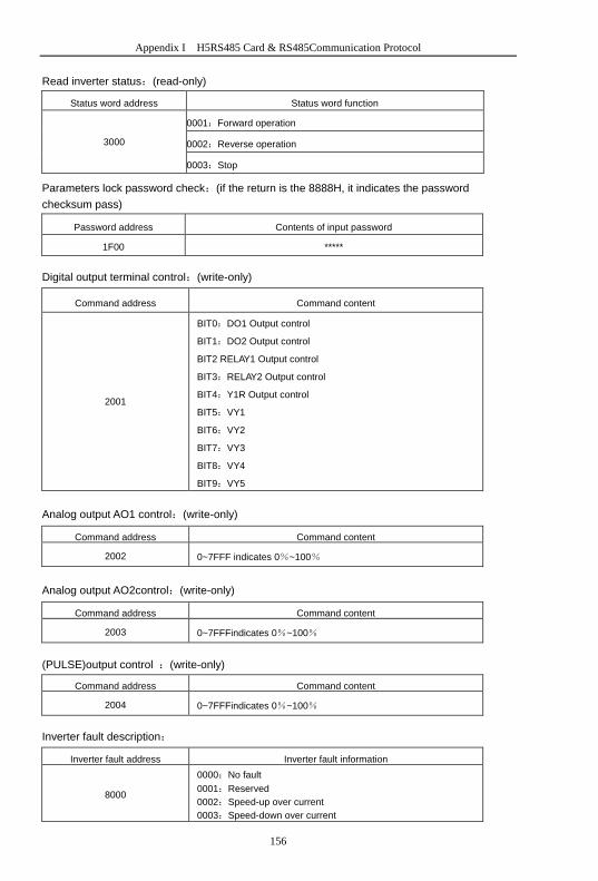
156
Appendix I H5RS485 Card & RS485Communication Protocol
Read inverter status:(read-only)
Status word address Status word function
3000
0001:Forward operation
0002:Reverse operation
0003:Stop
Parameters lock password check:(if the return is the 8888H, it indicates the password
checksum pass)
Password address Contents of input password
1F00 *****
Digital output terminal control:(write-only)
Command address Command content
2001
BIT0:DO1 Output control
BIT1:DO2 Output control
BIT2 RELAY1 Output control
BIT3:RELAY2 Output control
BIT4:Y1R Output control
BIT5:VY1
BIT6:VY2
BIT7:VY3
BIT8:VY4
BIT9:VY5
Analog output AO1 control:(write-only)
Command address Command content
2002 0~7FFF indicates 0%~100%
Analog output AO2control:(write-only)
Command address Command content
2003 0~7FFFindicates 0%~100%
(PULSE)output control :(write-only)
Command address Command content
2004 0~7FFFindicates 0%~100%
Inverter fault description:
Inverter fault address Inverter fault information
8000
0000:No fault
0001:Reserved
0002:Speed-up over current
0003:Speed-down over current

157
Appendix I H5RS485 Card & RS485Communication Protocol
0004:Constant speed over current
0005:Speed-up over voltage
0006:Speed-DOWN over voltage
0007:Constant speed over voltage
0008:Buffer resistance overload fault
0009:Under-voltage fault
000A:Inverter overload
000B:Motor overload
000C:Input phase lost
000D:Output phase lost
000E:Module overheating
000F:External fault
0010:Communication fault
0011:Contactor fault
0012:Current detection fault
0013:Motor tuning fault
0014:Encoder/PG card fault
0015:Parameter read and write fault
0016:Inverter hardware fault
0017:Motor earthing short-circuit fault
0018:Reserved
0019:Reserved
001A:Running time arrive fault
001B:User defined fault 1
001C:User defined fault 2
001D:Power on time arrive fault
001E:Load off
001F:PID feedback lost during operation
0028:Fast current limit timeout fault
0029:Motor shifting fault during operation
002A:Excessive speed deviation
002B:Motor over speed
002D:Motor over-temperature
005A:Encoder line number setup fault
005B:Encoder not connected
005C:Initial position error
005E:Speed feedback fault
Communication fault information describing data (fault code):
Communication fault address Fault function description
8001
0000:No fault 0001:Password error 0002:Command code error 0003:CRC check error
0004:Invalid address 0005:Invalid parameter
0006:Parameter change invalid 0007:The system is locked
0008:Operating EEPROM
Pd group communication parameters description
Pd.00
Baud rate Factory default value 6005
Setup range
1 bit:MODUBS baud rate
0:300BPS 1:600BPS
2:1200BPS 3:2400BPS
4:4800BPS 5:9600BPS
6:19200BPS 7:38400BPS
8:57600BPS 9:115200BPS
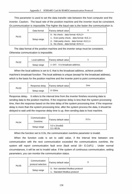
158
Appendix I H5RS485 Card & RS485Communication Protocol
This parameter is used to set the data transfer rate between the host computer and the
inverter. Caution:The baud rate of the position machine and the inverter must be consistent.
Or,communication is impossible.The higher the baud rate is,the faster the communication is.
Pd.01
Data format Factory default value 0
Setup range
0:No check:data format <8,N,2>
1:Even parity check:data format <8,E,1>
2:Odd parity check:data format <8,O,1>
3:No check:data format <8-N-1>
The data format of the position machine and the inverter setup must be consistent,
Otherwise communication is impossible.
Pd.02
Local address Factory default value 1
Setup range 1~247,0 is broadcast address.
When the local address is set to 0, that is the broadcast address, achieve position
machine’s broadcast function. The local address is unique (except for the broadcast address),
which is the basis for the position machine and the inverter point to point communication.
Pd.03
Response delay Factory default value 2ms
Setup range 0~20ms
Response delay: It refers to the interval time from the inverter finishes receiving data to
sending data to the position machine. If the response delay is less than the system processing
time, then the response based on the time delay of the system processing time. If the response
delay is more than the system processing time, after the system process the data, it should be
delayed to wait until the response delay time is up, then sending data to host machine.
Pd.04
Communication
Overtime Factory default value 0.0 s
Setup range 0.0 s (Invalid)
0.1~60.0s
When the function set to 0.0s, the communication overtime parameter is invalid.
When the function code is set to valid value, if the interval time between one
communication with the next communication exceeded the communications overtime, the
system will report communication fault error (fault serial 16= E.CoF1) . Under normal
circumstances, it will be set to invalid value. If the system of continuous communication, setting
parameters, you can monitor the communication status.
Pd.05
Communication
protocol selection Factory default value 0
Setup range 0:Non standard Modbus protocol
1:Standard Modbus protocol

159
Appendix I H5RS485 Card & RS485Communication Protocol
Pd.05=1:Select Standard Modbus protocol.
Pd.05=0:Reading command, the slave returns the number of bytes which has one more byte
than the standard Modbus protocol, for specific please refer to the protocol, the part of the "5
communication data structure”.
Pd.06
Communication
read the current
resolution
Factory default value 0
Setup range 0:0.01A
1:0.1A
To determine when the communication reads the output current, what the output current
value unit is.
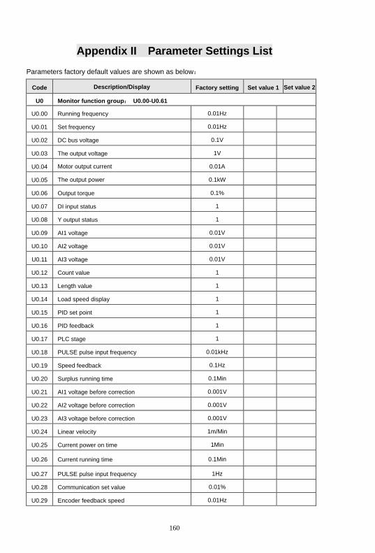
160
Appendix II Parameter Settings List
Parameters factory default values are shown as below:
Code Description/Display Factory setting Set value 1 Set value 2
U0 Monitor function group: U0.00-U0.61
U0.00 Running frequency 0.01Hz
U0.01 Set frequency 0.01Hz
U0.02 DC bus voltage 0.1V
U0.03 The output voltage 1V
U0.04 Motor output current 0.01A
U0.05 The output power 0.1kW
U0.06 Output torque 0.1%
U0.07 DI input status 1
U0.08 Y output status 1
U0.09 AI1 voltage 0.01V
U0.10 AI2 voltage 0.01V
U0.11 AI3 voltage 0.01V
U0.12 Count value 1
U0.13 Length value 1
U0.14 Load speed display 1
U0.15 PID set point 1
U0.16 PID feedback 1
U0.17 PLC stage 1
U0.18 PULSE pulse input frequency 0.01kHz
U0.19 Speed feedback 0.1Hz
U0.20 Surplus running time 0.1Min
U0.21 AI1 voltage before correction 0.001V
U0.22 AI2 voltage before correction 0.001V
U0.23 AI3 voltage before correction 0.001V
U0.24 Linear velocity 1m/Min
U0.25 Current power on time 1Min
U0.26 Current running time 0.1Min
U0.27 PULSE pulse input frequency 1Hz
U0.28 Communication set value 0.01%
U0.29 Encoder feedback speed 0.01Hz
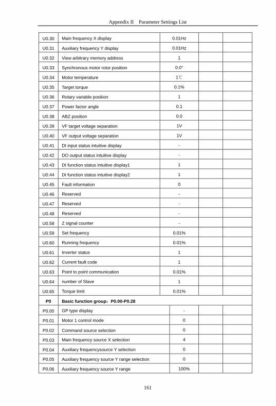
161
Appendix II Parameter Settings List
U0.30 Main frequency X display 0.01Hz
U0.31 Auxiliary frequency Y display 0.01Hz
U0.32 View arbitrary memory address 1
U0.33 Synchronous motor rotor position 0.0°
U0.34 Motor temperature 1
U0.35 Target torque 0.1%
U0.36 Rotary variable position 1
U0.37 Power factor angle 0.1
U0.38 ABZ position 0.0
U0.39 VF target voltage separation 1V
U0.40 VF output voltage separation 1V
U0.41 DI input status intuitive display -
U0.42 DO output status intuitive display -
U0.43 DI function status intuitive display1 1
U0.44 DI function status intuitive display2 1
U0.45 Fault information 0
U0.46 Reserved -
U0.47 Reserved -
U0.48 Reserved -
U0.58 Z signal counter -
U0.59 Set frequency 0.01%
U0.60 Running frequency 0.01%
U0.61 Inverter status 1
U0.62 Current fault code 1
U0.63 Point to point communication 0.01%
U0.64 number of Slave 1
U0.65 Torque limit 0.01%
P0 Basic function group:P0.00-P0.28
P0.00 GP type display -
P0.01 Motor 1 control mode 0
P0.02 Command source selection 0
P0.03 Main frequency source X selection 4
P0.04 Auxiliary frequencysource Y selection 0
P0.05 Auxiliary frequency source Y range selection 0
P0.06 Auxiliary frequency source Y range 100%
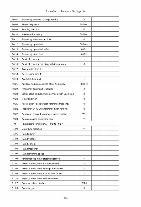
162
Appendix II Parameter Settings List
P0.07 Frequency source stacking selection 00
P0.08 Preset frequency 50.00Hz
P0.09 Running direction 0
P0.10 Maximum frequency 50.00Hz
P0.11 Frequency source upper limit 0
P0.12 Frequency upper limit 50.00Hz
P0.13 Frequency upper limit offset 0.00Hz
P0.14 Frequency lower limit 0.00Hz
P0.15 Carrier frequency -
P0.16 Carrier frequency adjusting with temperature 0
P0.17 Acceleration time 1 -
P0.18 Deceleration time 1 -
P0.19 Acc./ dec. time unit 1
P0.21 Auxiliary frequency source offset frequency 0.00Hz
P0.22 Frequency command resolution 2
P0.23 Digital setup frequency memory selection upon stop 0
P0.24 Motor selection 0
P0.25 Acceleration / deceleration reference frequency 0
P0.26 Frequency UP/DOWNreference upon running 0
P0.27 Command source& frequency source binding 000
P0.28 Communication expansion card 0
P1 Parameters for motor 1: P1.00-P0.37
P1.00 Motor type selection 0
P1.01 Rated power -
P1.02 Rated voltage -
P1.03 Rated current -
P1.04 Rated frequency -
P1.05 Rated revolving speed -
P1.06 Asynchronous motor stator resistance -
P1.07 Asynchronous motor rotor resistance -
P1.08 Asynchronous motor leakage inductance -
P1.09 Asynchronous motor mutual inductance -
P1.10 Asynchronous motor no load current -
P1.27 Encoder pulses number 2500
P1.28 Encoder type 0

163
Appendix II Parameter Settings List
P1.30 ABZ incremental encoder AB phase 0
P1.31 Encoder installation angle 0.00
P1.32 UVW phase sequence 0
P1.33 UVW encoder offset angle 0.00
P1.34 Rotary transformer pole pairs 1
P1.35 UVW pole-pairs 4
P1.36 PG dropped inspection time 0.0s
P1.37 Tuning selection 0
P2 Vector control function group: P2.00-P2.22
P2.00 Speed loop proportional gain 1 30
P2.01 Speed loop integration time1 0.50s
P2.02 Switching frequency1 5.00Hz
P2.03 Speed loop proportional gain 2 20
P2.04 Speed loop integration time 2 1.00s
P2.05 Switching frequency 2 10.00Hz
P2.06 Vector control slip gain 100%
P2.07 Speed-loop filter time 28
P2.08 Vector control over-excitation gain 64
P2.09 Torque upper limit source in speed control mode 0
P2.10 Torque upper limit digital setup in speed control
mode 150.0%
P2.13 Excitation regulation proportional gain 2000
P2.14 Excitation regulation integration gain 1300
P2.15 Torque regulation proportional gain 2000
P2.16 Torque regulation integration gain 1300
P2.17 Speed loop integration attribute 0
P2.18 Synchronous motor field weakening mode 1
P2.19 Synchronous motor field weakening depth 100%
P2.20 Maximum field weakening current 50%
P2.21 Field weakening auto regulation gain 100%
P2.22 Field weakening integration multiples 2
P3 V/F control group: P3.00-P3.15
P3.00 V/F curve setup 0
P3.01 Torque boost value -
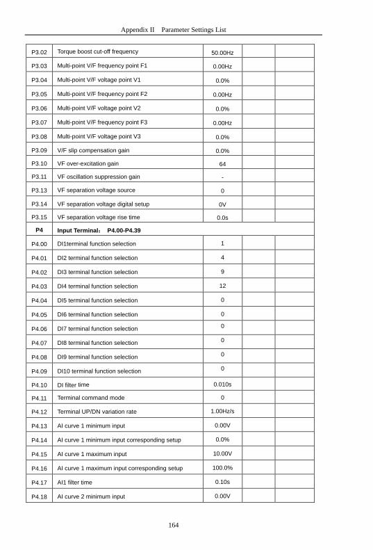
164
Appendix II Parameter Settings List
P3.02 Torque boost cut-off frequency 50.00Hz
P3.03 Multi-point V/F frequency point F1 0.00Hz
P3.04 Multi-point V/F voltage point V1 0.0%
P3.05 Multi-point V/F frequency point F2 0.00Hz
P3.06 Multi-point V/F voltage point V2 0.0%
P3.07 Multi-point V/F frequency point F3 0.00Hz
P3.08 Multi-point V/F voltage point V3 0.0%
P3.09 V/F slip compensation gain 0.0%
P3.10 VF over-excitation gain 64
P3.11 VF oscillation suppression gain -
P3.13 VF separation voltage source 0
P3.14 VF separation voltage digital setup 0V
P3.15 VF separation voltage rise time 0.0s
P4 Input Terminal: P4.00-P4.39
P4.00 DI1terminal function selection 1
P4.01 DI2 terminal function selection 4
P4.02 DI3 terminal function selection 9
P4.03 DI4 terminal function selection 12
P4.04 DI5 terminal function selection 0
P4.05 DI6 terminal function selection 0
P4.06 DI7 terminal function selection 0
P4.07 DI8 terminal function selection 0
P4.08 DI9 terminal function selection 0
P4.09 DI10 terminal function selection 0
P4.10 DI filter time 0.010s
P4.11 Terminal command mode 0
P4.12 Terminal UP/DN variation rate 1.00Hz/s
P4.13 AI curve 1 minimum input 0.00V
P4.14 AI curve 1 minimum input corresponding setup 0.0%
P4.15 AI curve 1 maximum input 10.00V
P4.16 AI curve 1 maximum input corresponding setup 100.0%
P4.17 AI1 filter time 0.10s
P4.18 AI curve 2 minimum input 0.00V
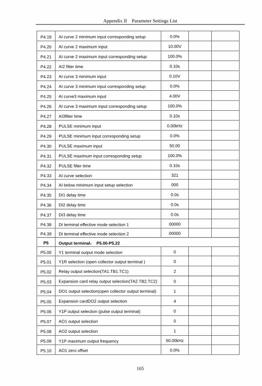
165
Appendix II Parameter Settings List
P4.19 AI curve 2 minimum input corresponding setup 0.0%
P4.20 AI curve 2 maximum input 10.00V
P4.21 AI curve 2 maximum input corresponding setup 100.0%
P4.22 AI2 filter time 0.10s
P4.23 AI curve 3 minimum input 0.10V
P4.24 AI curve 3 minimum input corresponding setup 0.0%
P4.25 AI curve3 maximum input 4.00V
P4.26 AI curve 3 maximum input corresponding setup 100.0%
P4.27 AI3filter time 0.10s
P4.28 PULSE minimum input 0.00kHz
P4.29 PULSE minimum input corresponding setup 0.0%
P4.30 PULSE maximum input 50.00
P4.31 PULSE maximum input corresponding setup 100.0%
P4.32 PULSE filter time 0.10s
P4.33 AI curve selection 321
P4.34 AI below minimum input setup selection 000
P4.35 DI1 delay time 0.0s
P4.36 DI2 delay time 0.0s
P4.37 DI3 delay time 0.0s
P4.38 DI terminal effective mode selection 1 00000
P4.39 DI terminal effective mode selection 2 00000
P5 Output terminal: P5.00-P5.22
P5.00 Y1 terminal output mode selection 0
P5.01 Y1R selection (open collector output terminal ) 0
P5.02 Relay output selection(TA1.TB1.TC1) 2
P5.03 Expansion card relay output selection(TA2.TB2.TC2) 0
P5.04 DO1 output selection(open collector output terminal) 1
P5.05 Expansion cardDO2 output selection 4
P5.06 Y1P output selection (pulse output terminal) 0
P5.07 AO1 output selection 0
P5.08 AO2 output selection 1
P5.09 Y1P maximum output frequency 50.00kHz
P5.10 AO1 zero offset 0.0%
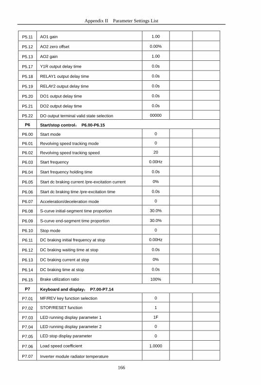
166
Appendix II Parameter Settings List
P5.11 AO1 gain 1.00
P5.12 AO2 zero offset 0.00%
P5.13 AO2 gain 1.00
P5.17 Y1R output delay time 0.0s
P5.18 RELAY1 output delay time 0.0s
P5.19 RELAY2 output delay time 0.0s
P5.20 DO1 output delay time 0.0s
P5.21 DO2 output delay time 0.0s
P5.22 DO output terminal valid state selection 00000
P6 Start/stop control: P6.00-P6.15
P6.00 Start mode 0
P6.01 Revolving speed tracking mode 0
P6.02 Revolving speed tracking speed 20
P6.03 Start frequency 0.00Hz
P6.04 Start frequency holding time 0.0s
P6.05 Start dc braking current /pre-excitation current 0%
P6.06 Start dc braking time /pre-excitation time 0.0s
P6.07 Acceleration/deceleration mode 0
P6.08 S-curve initial-segment time proportion 30.0%
P6.09 S-curve end-segment time proportion 30.0%
P6.10 Stop mode 0
P6.11 DC braking initial frequency at stop 0.00Hz
P6.12 DC braking waiting time at stop 0.0s
P6.13 DC braking current at stop 0%
P6.14 DC braking time at stop 0.0s
P6.15 Brake utilization ratio 100%
P7 Keyboard and display: P7.00-P7.14
P7.01 MF/REV key function selection 0
P7.02 STOP/RESET function 1
P7.03 LED running display parameter 1 1F
P7.04 LED running display parameter 2 0
P7.05 LED stop display parameter 0
P7.06 Load speed coefficient 1.0000
P7.07 Inverter module radiator temperature

167
Appendix II Parameter Settings List
P7.08 product ID
P7.09 Accumulative running time 0h
P7.10 Performance version number -
P7.11 Software version No. -
P7.12 Load speed display decimal digits 1
P7.13 Accumulative power-on time -
P7.14 Accumulative power consumption -
P8 Auxiliary Function: P8.00-P8.53
P8.00 Jog running frequency 2.00Hz
P8.01 Jog acceleration time 20.0s
P8.02 Jog deceleration time 20.0s
P8.03 Acceleration time 2 10.0s
P8.04 Deceleration time 2 10.0s
P8.05 Acceleration time 3 10.0s
P8.06 Deceleration time 3 10.0s
P8.07 Acceleration time 4 10.0s
P8.08 Deceleration time 4 10.0s
P8.09 Hopping frequency 1 0.00Hz
P8.10 Hopping frequency 2 0.00Hz
P8.11 Hopping frequency amplitude 0.00Hz
P8.12 Dead zone time of forward & reverse rotations 0.0s
P8.13 Reverse rotation control 0
P8.14 Set frequency below lower limit running mode 0
P8.15 Droop control 0.00Hz
P8.16 Accumulative power-on time arrival setup 0h
P8.17 Accumulative running time arrival setup 0h
P8.18 Start protection selection 0
P8.19 Frequency detection value (FDT1) 50.00Hz
P8.20 Frequency detection hysteresis value (FDT1) 5.0%
P8.21 Frequency arrival detection amplitude 0.0%
P8.22 Acc./dec. hopping frequency validity 0
P8.25 Acc. time1 & acc. time 2 frequency switching point 0.00Hz
P8.26 Dec. time1 & dec. time 2 frequency switching point 0.00Hz
P8.27 Terminal jog priority 0

168
Appendix II Parameter Settings List
P8.28 Frequency detection value(FDT2) 50.00Hz
P8.29 Frequency detection hysteresis value(FDT2) 5.0%
P8.30 Random frequency arrival detection value1 50.00Hz
P8.31 Random frequency arrival detection range1 0.0%
P8.32 Random frequency arrival detection value2 50.00Hz
P8.33 Random frequency arrival detection range2 0.0%
P8.34 Zero-current detection level 5.0%
P8.35 Zero-current detection delay time 0.10s
P8.36 Output current overlimit value 200.0%
P8.37 Output current overlimit detection delay time 0.00s
P8.38 Random current arrival 1 100.0%
P8.39 Random current arrival range1 0.0%
P8.40 Random current arrival 2 100.0%
P8.41 Random current arrival range2 0.0%
P8.42 Timing function selection 0
P8.43 Running time timing selection 0
P8.44 Timing running time 0.0Min
P8.45 AI1 input voltage protection value lower limit 3.10V
P8.46 AI1 input voltage protection value upper limit 6.80V
P8.47 Module temperature arrival 75
P8.48 Cooling fan control 0
P8.49 Wake-up frequency 0.00Hz
P8.50 Wake-up delay time 0.0s
P8.51 Sleep frequency 0.00Hz
P8.52 Sleep delay time 0.0s
P8.53 The running time arrival 0.0Min
P9 Overload and Protection: P9.00-P9.70
P9.00 Motor overload protection selection 1
P9.01 Motor overload protection gain 1.00
P9.02 Motor overload pre-alarm coefficient 80%
P9.03 Over-voltage stall gain 0
P9.04 Over-voltage stall protection voltage 130%
P9.05 Over current stall gain 20
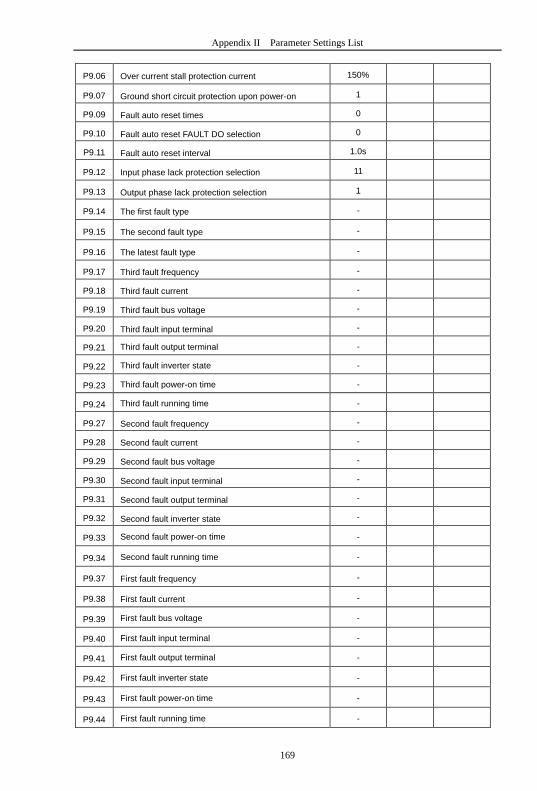
169
Appendix II Parameter Settings List
P9.06 Over current stall protection current 150%
P9.07 Ground short circuit protection upon power-on 1
P9.09 Fault auto reset times 0
P9.10 Fault auto reset FAULT DO selection 0
P9.11 Fault auto reset interval 1.0s
P9.12 Input phase lack protection selection 11
P9.13 Output phase lack protection selection 1
P9.14 The first fault type -
P9.15 The second fault type -
P9.16 The latest fault type -
P9.17 Third fault frequency -
P9.18 Third fault current -
P9.19 Third fault bus voltage -
P9.20 Third fault input terminal -
P9.21 Third fault output terminal -
P9.22 Third fault inverter state -
P9.23 Third fault power-on time -
P9.24 Third fault running time -
P9.27 Second fault frequency -
P9.28 Second fault current -
P9.29 Second fault bus voltage -
P9.30 Second fault input terminal -
P9.31 Second fault output terminal -
P9.32 Second fault inverter state -
P9.33 Second fault power-on time -
P9.34 Second fault running time -
P9.37 First fault frequency -
P9.38 First fault current -
P9.39 First fault bus voltage -
P9.40 First fault input terminal -
P9.41 First fault output terminal -
P9.42 First fault inverter state -
P9.43 First fault power-on time -
P9.44 First fault running time -
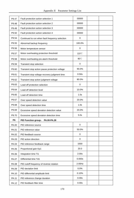
170
Appendix II Parameter Settings List
P9.47 Fault protection action selection 1 00000
P9.48 Fault protection action selection 2 00000
P9.49 Fault protection action selection 3 00000
P9.50 Fault protection action selection 4 00000
P9.54 Continued to run when fault frequency selection 0
P9.55 Abnormal backup frequency 100.0%
P9.56 Motor temperature sensor 0
P9.57 Motor overheating protection threshold 110
P9.58 Motor overheating pre-alarm threshold 90
P9.59 Transient stop selection 0
P9.60 Transient stop action pause protection voltage 90.0%
P9.61 Transient stop voltage recovery judgment time 0.50s
P9.62 Transient stop action judgment voltage 80.0%
P9.63 Load-off protection selection 0
P9.64 Load-off detection level 10.0%
P9.65 Load-off detection time 1.0s
P9.67 Over speed detection value 20.0%
P9.68 Over speed detection time 1.0s
P9.69 Excessive speed deviation detection value 20.0%
P9.70 Excessive speed deviation detection time 5.0s
PA PID Function group: PA.00-PA.28
PA.00 PID reference source 0
PA.01 PID reference value 50.0%
PA.02 PID feedback source 0
PA.03 PID action direction 0
PA.04 PID reference feedback range 1000
PA.05 Proportional gain Kp1 20.0
PA.06 Integration time Ti1 2.00s
PA.07 Differential time Td1 0.000s
PA.08 PID cutoff frequency of reverse rotation 2.00Hz
PA.09 PID deviation limit 0.0%
PA.10 PID differential amplitude limit 0.10%
PA.11 PID reference change duration 0.00s
PA.12 PID feedback filter time 0.00s

171
Appendix II Parameter Settings List
PA.13 PID output filter time 0.00s
PA.14 Reserved -
PA.15 Proportional gain Kp2 20.0
PA.16 Integration time Ti2 2.00s
PA.17 Differential time Td2 0.000s
PA.18 PID parameter switching condition 0
PA.19 PID parameter switching deviation1 20.0%
PA.20 PID parameter switching deviation2 80.0%
PA.21 PID initial value 0.0%
PA.22 PID initial value retention time 0.00s
PA.23 Output deviation forward maximum value 1.00%
PA.24 Output deviation reverse maximum value 1.00%
PA.25 PID integration attribute 00
PA.26 PID feedback loss detection value 0.0%
PA.27 PID feedback loss detection time 0s
PA.28 PID stop operation 0
Pb Swing Frequency, Fixed Length and Counting: Pb.00-Pb.09
Pb.00 Swing setup mode 0
Pb.01 Swing frequency amplitude 0.0%
Pb.02 Jump frequency amplitude 0.0%
Pb.03 Swing frequency cycle 10.0s
Pb.04 Triangle wave rise time coefficient 50.0%
Pb.05 Setup length 1000m
Pb.06 Actual length 0m
Pb.07 Pulse number per meter 100.0
Pb.08 Counting value setup 1000
Pb.09 Designated counting value 1000
PC MS Speed Function & Simple PLC Function: PC.00-PC.51
PC.00 MS command 0 0.0%
PC.01 MS command 1 0.0%
PC.02 MS command 2 0.0%
PC.03 MS command 3 0.0%
PC.04 MS command 4 0.0%
172
Appendix II Parameter Settings List
PC.05 MS command 5 0.0%
PC.06 MS command 6 0.0%
PC.07 MS command 7 0.0%
PC.08 MS command 8 0.0%
PC.09 MS command 9 0.0%
PC.10 MS command 10 0.0%
PC.11 MS command 11 0.0%
PC.12 MS command 12 0.0%
PC.13 MS command 13 0.0%
PC.14 MS command 14 0.0%
PC.15 MS command 15 0.0%
PC.16 PLC running mode 0
PC.17 PLC power off memory selection 00
PC.18 PLC 0segment running time 0.0s(h)
PC.19 PLC 0segment acc./dec. time 0
PC.20 PLC 1segment running time 0.0s(h)
PC.21 PLC 1segment acc./dec. time 0
PC.22 PLC 2 segment running time 0.0s(h)
PC.23 PLC 2 segment acc./dec. time 0
PC.24 PLC 3 segment running time 0.0s(h)
PC.25 PLC 3 segment acc./dec. time 0
PC.26 PLC 4 segment running time 0.0s(h)
PC.27 PLC 4 segment acc./dec. time 0
PC.28 PLC 5 segment running time 0.0s(h)
PC.29 PLC 5 segment acc./dec. time 0
PC.30 PLC 6 segment running time 0.0s(h)
PC.31 PLC 6 segment acc./dec. time 0
PC.32 PLC 7 segment running time 0.0s(h)
PC.33 PLC 7 segment acc./dec. time 0
PC.34 PLC 8 segment running time 0.0s(h)
PC.35 PLC 8 segment acc./dec. time 0
PC.36 PLC 9 segment running time 0.0s(h)
PC.37 PLC 9 segment acc./dec. time 0

173
Appendix II Parameter Settings List
PC.38 PLC 10 segment running time 0.0s(h)
PC.39 PLC 10 segment acc./dec. time 0
PC.40 PLC 11 segment running time 0.0s(h)
PC.41 PLC 11 segment acc./dec. time 0
PC.42 PLC 12 segment running time 0.0s(h)
PC.43 PLC 12 segment acc./dec. time 0
PC.44 PLC 13 segment running time 0.0s(h)
PC.45 PLC 13 segment acc./dec. time 0
PC.46 PLC 14 segment running time 0.0s(h)
PC.47 PLC 14 segment acc./dec. time 0
PC.48 PLC 15 segment running time 0.0s(h)
PC.49 PLC 15 segment acc./dec. time 0
PC.50 Running time unit 0
PC.51 MS command 0 reference mode 0
Pd Communication function group:Pd.00-Pd.29
Pd.00 Baud rate 6005
Pd.01 Data format 0
Pd.02 Local address 1
Pd.03 Response delay 2
Pd.04 Excessive communication time 0.0
Pd.05 Data transformat selection 30
Pd.06 Communication read current resolution 0
PE User customization function code: PE.00-PE.29
PE.00 User function code 0 P0.01
PE.01 User function code 1 P0.02
PE.02 User function code 2 P0.03
PE.03 User function code 3 P0.07
PE.04 User function code 4 P0.08
PE.05 User function code 5 P0.17
PE.06 User function code 6 P0.18
PE.07 User function code 7 P3.00
PE.08 User function code 8 P3.01
PE.09 User function code 9 P4.00
174
Appendix II Parameter Settings List
PE.10 User function code 10 P4.01
PE.11 User function code 11 P4.02
PE.12 User function code 12 P5.04
PE.13 User function code 13 P5.07
PE.14 User function code 14 P6.00
PE.15 User function code 15 P6.10
PE.16 User function code 16 P0.00
PE.17 User function code 17 P0.00
PE.18 User function code 18 P0.00
PE.19 User function code 19 P0.00
PE.20 User function code 20 P0.00
PE.21 User function code 21 P0.00
PE.22 User function code 22 P0.00
PE.23 User function code 23 P0.00
PE.24 User function code 24 P0.00
PE.25 User function code 25 P0.00
PE.26 User function code 26 P0.00
PE.27 User function code 27 P0.00
PE.28 User function code 28 P0.00
PE.29 User function code 29 P0.00
PP Function code management: PP.00-PP.04
PP.00 User password 0
PP.01 Parameter initialization 0
PP.02 Parameter display attribute 11
PP.03 Personalized parameter display selection 00
PP.04 Function codes modification attribute 0
A0 Torque control group: A0.00-A0.08
A0.00 Speed/ torque control mode selection 0
A0.01 Torque setup source selection in torque control mode 0
A0.03 Torque digital setup in torque control mode 150%
A0.05 Torque control forward maximum frequency 50.00Hz
A0.06 Torque control reverse maximum frequency 50.00Hz
A0.07 Torque control acc. time 0.00s
A0.08 Torque control dec. time 0.00s

175
Appendix II Parameter Settings List
A1 Virtual IO: A1.00-A1.21
A1.00 Virtual VDI1 function selection 0
A1.01 Virtual VDI2 function selection 0
A1.02 Virtual VDI3 function selection 0
A1.03 Virtual VDI4 function selection 0
A1.04 Virtual VDI5 function selection 0
A1.05 Virtual VD1 terminal valid state set mode 00000
A1.06 Virtual VD1 terminal state 00000
A1.07 AI1 as DI function selection 0
A1.08 AI2 as DI function selection 0
A1.09 AI3 as DI function selection 0
A1.10 AI as DI valid mode selection 000
A1.11 Virtual VDO1 output function 0
A1.12 Virtual VDO2 output function 0
A1.13 Virtual VDO3 output function 0
A1.14 Virtual VDO4 output function 0
A1.15 Virtual VDO5 output function 0
A1.16 VDO1 output delay time 0.0s
A1.17 VDO2 output delay time 0.0s
A1.18 VDO3 output delay time 0.0s
A1.19 VDO4 output delay time 0.0s
A1.20 VDO5 output delay time 0.0s
A1.21 VDO output terminal valid state selection 00000
A2 The second motor control: A2.00-A2.65
A2.00 Motor type selection 0
A2.01 Rated power -
A2.02 Rated voltage -
A2.03 Rated current -
A2.04 Rated frequency -
A2.05 Rated revolving speed -
A2.06 Asynchronous motor stator resistance -
A2.07 Asynchronous motor rotor resistance -
A2.08 Asynchronous motor leakage inductance -
176
Appendix II Parameter Settings List
A2.09 Asynchronous motor mutual inductance -
A2.10 Asynchronous motor no load current -
A2.16 Synchronous motor stator resistance -
A2.17 Synchronous motor D-axis inductance -
A2.18 Synchronous motor Q-axis inductance -
A2.19 Synchronous motor
inductance resistance unit 0
A2.20 Synchronous motor back electromotive force
coefficient. 0.1V
A2.21 Synchronous motor output phase lack
detection time 0
A2.27 Encoder pulses number 2500
A2.28 Encoder type 0
A2.29 Speed feedback PG selection 0
A2.30 ABZ incremental encoder AB phase 0
A2.31 Encoder installation angle 0
A2.32 UVW phase sequence 0
A2.33 UVW encoder offset angle 0.00
A2.34 Rotary transformer pole pairs 1
A2.35 UVW pole-pairs 4
A2.36 PG dropped inspection time 0.0s
A2.37 Tuning selection 0
A2.38 Speed loop proportional gain 1 30
A2.39 Speed loop integration time1 0.50s
A2.40 Switching frequency1 5.00Hz
A2.41 Speed loop proportional gain 2 20
A2.42 Speed loop integration time 2 1.00s
A2.43 Switching frequency 2 10.00Hz
A2.44 Vector control slip gain 150%
A2.45 Speed-loop filtering time 0.000s
A2.46 Vector control over-excitation gain 64
A2.47 Torque upper limit source in speed control
mode 0
A2.48 Torque upper limit digital setup in speed
control mode 150.0%
A2.51 Excitation regulation proportional gain 2000
177
Appendix II Parameter Settings List
A2.52 Excitation regulation integration gain 1300
A2.53 Torque regulation proportional gain 2000
A2.54 Torque regulation integration gain 1300
A2.55 Speed loop integration attribute 0
A2.56 Synchronous motor field weakening mode 1
A2.57 Synchronous motor field weakening depth 100%
A2.58 Maximum field weakening current 50%
A2.59 Field weakening auto regulation gain 100%
A2.60 Field weakening integration multiples 2
A2.61 Motor2 control mode 0
A2.62 Motor 2 acc./dec. time selection 0
A2.63 Motor 2 torque hoist -
A2.65 Motor 2 oscillation suppression gain -
A5 Control optimization group:A5.00-A5.09
A5.00 DPWM switching frequency upper limit 12.00Hz
A5.01 PWM modulation mode 0
A5.02 Dead-zone compensation mode selection 1
A5.03 Random PWM depth 0
A5.04 Rapid current-limiting enable 1
A5.05 Current detection compensation 5
A5.06 Under-voltage point setup 100.0%
A5.07 SVC optimization mode selection 1
A5.08 Dead zone time adjustment 150%
A5.09 Over-voltage point setup Model determination
A6 AI curve setup: A6.00-A6.29
A6.00 AI curve 4 minimum input 0.00V
A6.01 AI curve 4 minimum input corresponding
setup 0.0%
A6.02 AI curve 4inflection point 1 input 3.00V
A6.03 AI curve 4 inflection point 1 input
corresponding setup 30.0%
A6.04 AI curve 4 inflection point 2 input 6.00V
A6.05 AI curve 4 inflection point 2 input
corresponding setup 60.0%
A6.06 AI curve 4 maximum input 10.00V
A6.07 AI curve 4 maximum input corresponding
setup 100.0%
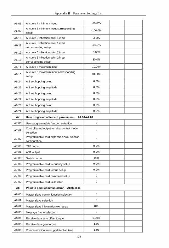
178
Appendix II Parameter Settings List
A6.08 AI curve 4 minimum input -10.00V
A6.09 AI curve 5 minimum input corresponding
setup -100.0%
A6.10 AI curve 5 inflection point 1 input -3.00V
A6.11 AI curve 5 inflection point 1 input
corresponding setup -30.0%
A6.12 AI curve 5 inflection point 2 input 3.00V
A6.13 AI curve 5 inflection point 2 input
corresponding setup 30.0%
A6.14 AI curve 5 maximum input 10.00V
A6.15 AI curve 5 maximum input corresponding
setup 100.0%
A6.24 AI1 set hopping point 0.0%
A6.25 AI1 set hopping amplitude 0.5%
A6.26 AI2 set hopping point 0.0%
A6.27 AI2 set hopping amplitude 0.5%
A6.28 AI3 set hopping point 0.0%
A6.29 AI3 set hopping amplitude 0.5%
A7 User programmable card parameters: A7.00-A7.09
A7.00 User programmable function selection 0
A7.01 Control board output terminal control mode
selection -
A7.02 Programmable card expansion AI3x function
configuration -
A7.03 Y1P output 0.0%
A7.04 AO1 output 0.0%
A7.05 Switch output 000
A7.06 Programmable card frequency setup 0.0%
A7.07 Programmable card torque setup 0.0%
A7.08 Programmable card command setup 0
A7.09 Programmable card fault setup 0
A8 Point to point communication:A8.00-8.11
A8.00 Master slave control function selection 0
A8.01 Master slave selection 0
A8.02 Master slave information exchange 011
A8.03 Message frame selection 0
A8.04 Receive data zero offset torque 0.00%
A8.05 Receive data gain torque 1.00
A8.06 Communication interrupt detection time 1.0s

179
Appendix II Parameter Settings List
A8.07 Communication Master data transmission
cycle 0.001s
A8.08 Receive data zero offset frequency 0.00%
A8.09 Receive data gain frequency 1.00
A8.10 Reverse
A8.11 view 0.5Hz
A9 Extended function group:A9.00-A9.09
A9.00 0
A9.01 0
A9.02 0
A9.03 0
A9.04 0
A9.05 0
A9.06 0
A9.07 0
A9.08 0
A9.09 0
AC AIAO correction: AC.00-AC.19
AC.00 AI1measured voltage 1 Factory calibration
AC.01 AI1 display voltage 1 Factory calibration
AC.02 AI1 measured voltage 2 Factory calibration
AC.03 AI1 display voltage 2 Factory calibration
AC.04 AI2 measured voltage 1 Factory calibration
AC.05 AI2 display voltage 1 Factory calibration
AC.06 AI2 measured voltage 2 Factory calibration
AC.07 AI2 display voltage 2 Factory calibration
AC.08 AI3 measured voltage 1 Factory calibration
AC.09 AI3 display voltage 1 Factory calibration
AC.10 AI3 measured voltage 2 Factory calibration
AC.11 AI3 display voltage 2 Factory calibration
AC.12 A01 target voltage 1 Factory calibration
AC.13 A01 measured voltage 1 Factory calibration
AC.14 A01 target voltage 2 Factory calibration
AC.15 A01 measured voltage 2 Factory calibration
AC.16 A02 target voltage 1 Factory calibration

180
Appendix II Parameter Settings List
AC.17 A02 measured voltage 1 Factory calibration
AC.18 A02 target voltage 2 Factory calibration
AC.19 A02 measured voltage 2 Factory calibration
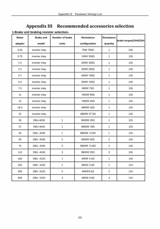
181
Appendix II Parameter Settings List
Appendix III Recommended accessories selection 1.Brake unit braking resistor selection:
Motor
adapter
Brake unit
model
Number of brake
units
Resistance
configuration
Resistance
quantity
brake torque(10%ED)%
0.40 inverter inlay 70W 750Ω 1 230
0.75 inverter inlay 100W 300Ω 1 130
1.5 inverter inlay 200W 300Ω 1 125
2.2 inverter inlay 200W 200Ω 1 135
3.7 inverter inlay 400W 150Ω 1 135
5.5 inverter inlay 500W 100Ω 1 135
7.5 inverter inlay 800W 75Ω 1 130
11 inverter inlay 1000W 60Ω 1 135
15 inverter inlay 1560W 45Ω 1 125
18.5 inverter inlay 4800W 32Ω 1 125
22 inverter inlay 4800W 27.2Ω 1 125
30 DBU-4030 1 6000W 20Ω 1 125
37 DBU-4045 1 9600W 16Ω 1 125
45 DBU -4045 1 9600W 13.6Ω 1 125
55 DBU -4030 2 6000W 20Ω 2 135
75 DBU -4045 2 9600W 13.6Ω 2 145
110 DBU -4030 3 9600W 20Ω 3 100
160 DBU -4220 1 40KW 3.4Ω 1 140
220 DBU -4220 1 60KW 3.2Ω 1 110
300 DBU -4220 2 40KW4.5Ω 2 110
600 DBU -4220 4 40KW 4.5Ω 4 110
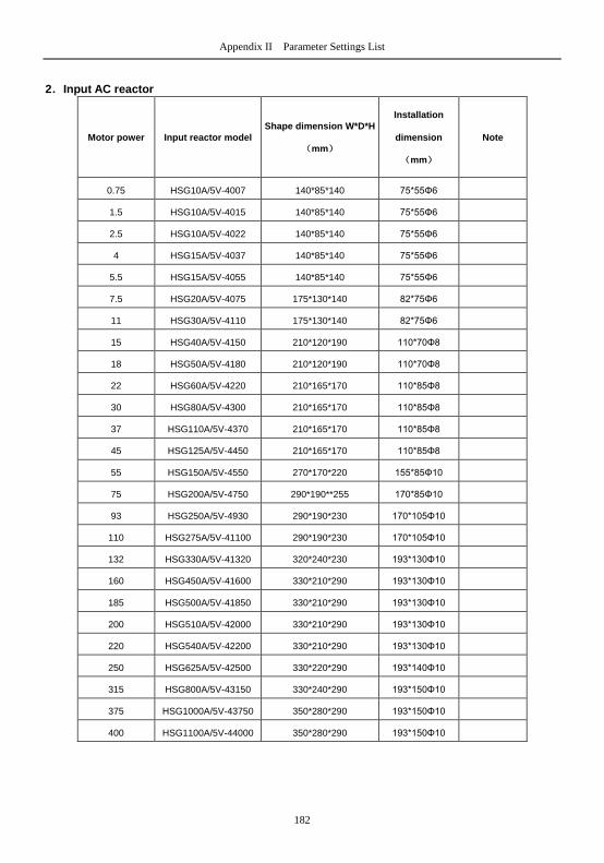
182
Appendix II Parameter Settings List
2.Input AC reactor
Motor power Input reactor model
Shape dimension W*D*H
(mm)
Installation
dimension
(mm)
Note
0.75 HSG10A/5V-4007 140*85*140 75*55Φ6
1.5 HSG10A/5V-4015 140*85*140 75*55Φ6
2.5 HSG10A/5V-4022 140*85*140 75*55Φ6
4 HSG15A/5V-4037 140*85*140 75*55Φ6
5.5 HSG15A/5V-4055 140*85*140 75*55Φ6
7.5 HSG20A/5V-4075 175*130*140 82*75Φ6
11 HSG30A/5V-4110 175*130*140 82*75Φ6
15 HSG40A/5V-4150 210*120*190 110*70Φ8
18 HSG50A/5V-4180 210*120*190 110*70Φ8
22 HSG60A/5V-4220 210*165*170 110*85Φ8
30 HSG80A/5V-4300 210*165*170 110*85Φ8
37 HSG110A/5V-4370 210*165*170 110*85Φ8
45 HSG125A/5V-4450 210*165*170 110*85Φ8
55 HSG150A/5V-4550 270*170*220 155*85Φ10
75 HSG200A/5V-4750 290*190**255 170*85Φ10
93 HSG250A/5V-4930 290*190*230 170*105Φ10
110 HSG275A/5V-41100 290*190*230 170*105Φ10
132 HSG330A/5V-41320 320*240*230 193*130Φ10
160 HSG450A/5V-41600 330*210*290 193*130Φ10
185 HSG500A/5V-41850 330*210*290 193*130Φ10
200 HSG510A/5V-42000 330*210*290 193*130Φ10
220 HSG540A/5V-42200 330*210*290 193*130Φ10
250 HSG625A/5V-42500 330*220*290 193*140Φ10
315 HSG800A/5V-43150 330*240*290 193*150Φ10
375 HSG1000A/5V-43750 350*280*290 193*150Φ10
400 HSG1100A/5V-44000 350*280*290 193*150Φ10

183
Appendix II Parameter Settings List
3.Output AC reactor
Motor power
KW
Output reactor model
Shape dimension W*D*H
(mm)
Installation
dimension
(mm)
Note
0.75 HSG10A/9V-4007 140*85*140 75*55Φ6
1.5 HSG10A/9V-4015 140*85*140 75*55Φ6
2.5 HSG10A/9V-4022 140*85*140 75*55Φ6
4 HSG15A/9V-4037 140*85*140 75*55Φ6
5.5 HSG15A/9V-4055 140*85*140 75*55Φ6
7.5 HSG20A/9V-4075 140*85*140 75*55Φ6
11 HSG30A/9V-4110 210*165*170 110*85Φ8
15 HSG40A/9V-4150 210*165*170 110*85Φ8
18 HSG50A/9V-4180 210*165*170 110*85Φ8
22 HSG60A/9V-4220 210*165*170 110*85Φ8
30 HSG80A/9V-4300 270*190*230 155*100Φ10
37 HSG110A/9V-4370 270*190*230 155*100Φ10
45 HSG125A/9V-4450 270*190*230 155*100Φ10
55 HSG150A/9V-4550 290*200*230 170*115Φ10
75 HSG200A/9V-4750 300*230*230 173*135Φ10
93 HSG250A/9V-4930 330*230*230 190*130Φ10
110 HSG275A/9V-41100 330*230*230 190*130Φ10
132 HSG330A/9V-41320 340*230*230 212*130Φ10
160 HSG450A/9V-41600 330*220*290 193*140Φ10
185 HSG500A/9V-41850 330*220*290 193*140Φ10
200 HSG510A/9V-42000 330*220*290 193*140Φ10
220 HSG540A/9V-42200 330*220*290 193*140Φ10
250 HSG625A/9V-42500 350*280*290 193*150Φ10
315 HSG800A/9V-43150 350*280*290 193*150Φ10
375 HSG1000A/9V-43750 400*300*350 240*200Φ10
400 HSG1100A/9V-44000 400*300*350 240*200Φ10

185
Product Feedback
Dear users:
Thank you for your interest and purchasing of HNC products!
HNC adheres to the "user-centric", based on customer demand, and offering full customer service to
enhance customer satisfaction.
We hope to learn about your present and future demand for HNC products as well as your valuable
feedback ofthe products. In order to help you get our service faster and more convenient, please visit our
company web site www.hncelectric.com for information feedback.
1) Download the product manual you need.
2) Read and download all kinds of product technical information, such as operation instruction, product
specification, features, FAQ, etc.
3) Application cases.
4) Technical consultation, on-line feedback
5) Feedback product information and customer requirement information by e-mail.
6) Inquiry for the latest products, obtain various types of warranty and extend additional service, etc.
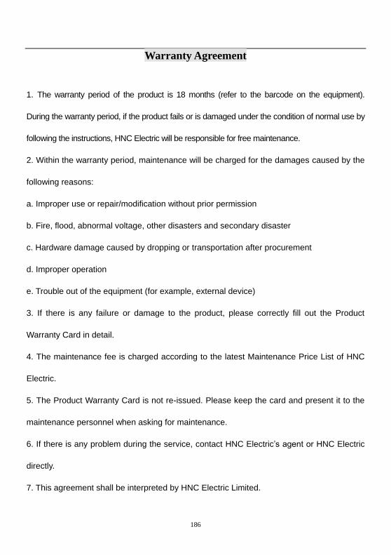
186
Warranty Agreement
1. The warranty period of the product is 18 months (refer to the barcode on the equipment).
During the warranty period, if the product fails or is damaged under the condition of normal use by
following the instructions, HNC Electric will be responsible for free maintenance.
2. Within the warranty period, maintenance will be charged for the damages caused by the
following reasons:
a. Improper use or repair/modification without prior permission
b. Fire, flood, abnormal voltage, other disasters and secondary disaster
c. Hardware damage caused by dropping or transportation after procurement
d. Improper operation
e. Trouble out of the equipment (for example, external device)
3. If there is any failure or damage to the product, please correctly fill out the Product
Warranty Card in detail.
4. The maintenance fee is charged according to the latest Maintenance Price List of HNC
Electric.
5. The Product Warranty Card is not re-issued. Please keep the card and present it to the
maintenance personnel when asking for maintenance.
6. If there is any problem during the service, contact HNC Electric’s agent or HNC Electric
directly.
7. This agreement shall be interpreted by HNC Electric Limited.

Version: 3.1.14
Thanks for choosing HNC product.
Any technique support, please feel free to contact
our support team
Tel: 86(20)84898493 Fax: 86(20)61082610
URL: www.hncelectric.com
Email: [email protected]