
Hitachi Accelerated Flash 2.0 - Whitepaper - Toolbox.com
20
Hitachi Accelerated Flash 2.0 An Innovative Approach to All-Flash Storage By Hitachi Vantara September 2018
-
Upload
khangminh22 -
Category
Documents
-
view
0 -
download
0
Transcript of Hitachi Accelerated Flash 2.0 - Whitepaper - Toolbox.com

Hitachi Accelerated Flash 2.0
An Innovative Approach to All-Flash Storage
By Hitachi Vantara
September 2018

1
Contents
Executive Summary ........................................................................................... 2
Introduction ....................................................................................................... 3
Flash Design Tradeoffs for Real-Enterprise Workloads ................................................................................ 3
Hitachi Accelerated Flash .................................................................................. 6
The Rise of Hitachi Accelerated Flash ............................................................................................................. 6
Hitachi Accelerated Flash Evolution ................................................................................................................ 7
Key Building Blocks of Hitachi Accelerated Flash ......................................................................................... 7
How HAF Innovation Extends the Endurance of Flash .................................................................................. 9
Architecture Highlights ..................................................................................... 10
Embedded Flash Controller ASIC .................................................................................................................. 10
Flash Controller Feature Highlights ............................................................................................................... 11
Flash Module DC2, FMD HD and FMD HDE Feature Highlights .................................................................. 15
Conclusion ...................................................................................................... 18
Appendix: External References........................................................................ 18

2
Executive Summary
Delivering on enterprise demands for real-time customer engagement requires more than a fast storage array. It
requires an end-to-end approach to data management that leverages both the storage operating system and flash
media, to deliver low latency performance even as data levels grow exponentially.
Current all-flash arrays (AFAs) rely on performance management to be handled in the array controller along with all
other operations, such as data reduction. As data levels increase, they can cause controller bottlenecks, sporadic
response times and a poor customer experience. To offset this issue, IT organizations have been forced to make
tradeoffs in the number of workloads or amount of data they store on an individual AFA. These decisions result in
the need to deploy and support more systems, raising costs and increasing management complexity.
Hitachi understands this and has enhanced Hitachi Storage Virtualization Operating System RF (SVOS RF), which
powers our award-winning Hitachi Virtual Storage Platforms (VSP). Storage Virtualization Operating System
integrated with Hitachi Accelerated Flash (HAF) fundamentally changes this paradigm. Now organizations can
engage customers faster, simplify storage operations and leverage the cloud for a superior return on investment.
HAF is powered with flash optimizations to SVOS RF and unique solid-state hardware design. This approach
eliminates these performance tradeoffs and answers demands for intelligent high performance, predictable, sub-
millisecond response time and improved data center efficiency.
With more than 350 flash patents, SVOS RF optimizations are engineered to accelerate the I/O path for access to
flash devices. The result is a complete “flash-accelerated” refresh of the operating system that delivers significantly
improved I/O processing, higher multithreading support and faster internal data movement. It also reduces response
times considerably. With SVOS RF, organizations benefit:
▪ Flash-aware I/O stack accelerates data access.
▪ Leading storage virtualization consolidates investments.
▪ Best-in-class business continuity prevents outages.
▪ Adaptive data reduction services reduce storage needs.
▪ Direct connect to cloud assures predictable, ongoing IT costs.
The second, third and encrypted generations of flash modules (FMD DC2, FMD HD, FMD HDE) on Virtual Storage
Platform are built from the ground up to support concurrent, large I/O enterprise workloads and enable hyperscale
efficiencies. At its core is an advanced embedded multicore flash controller that increases the performance of flash
to levels that exceed commodity solid-state drives (SSDs). They intelligently manage I/O and have the ability to
prioritize application I/O requests over background tasks, such as garbage collection, to minimize potential latency.
Although FMDs use NAND flash, they are not SSDs. The FMD is larger and longer than a traditional 2.5- or 3.5-inch
SSD; its rackmount design better utilizes the full depth of typical 19-inch data center rack. It enables leading, real-
application performance, with 150K 8KB random read I/O, with up three times the random read and five times the
random write performance of SSDs. It delivers a lower effective cost, with up to 70% lower effective bit price as well
as up to 60% faster response times1. Running on Hitachi VSP family systems, HAF enables sub-millisecond
delivery on a petabyte scale.
The purpose of this white paper is to take a close look at Hitachi Accelerated Flash. The discussion focuses on the
uniqueness of this solution. It considers why and how these technologies can meet the increasing IT challenges of
large and small enterprises as they focus on the management challenges of their high-velocity data.
1 “on 1.6TB SSD OEM price and 2:1 typical compression ratio.

3
Introduction
Flash Design Tradeoffs for Real-Enterprise Workloads
For storage architects and engineers designing high-performance application environments, flash can deliver
significant performance, response time and environmental benefits. However, these must be balanced against cost
and potential performance reductions that can occur when technologies like deduplication and compression are
enabled. When considering performance, four criteria define the performance envelope of a flash drive: interconnect
to the host, the embedded flash controller performance, the NAND package (chip) array, and power. The flash
translation layer or FTL aggregates all these resources to enable a singular block of addresses that span across
many NAND packages.
Workload I/O profiles that are random-read intensive will tax the most the embedded flash controller and
interconnect the most, requiring an efficient FTL to handle concurrent commands. Write-intensive random-I/O
scaling will be limited by the NAND array and available power (operating temperature) to drive as many channels
and NAND packages in parallel. Write scalability limits and response times will be defined by the amount of memory
and bandwidth available to the FTL, to process requests related to NAND cell mapping.
The following sections will break down core flash components and concepts, while also assessing quality and price
differences between flash technology options. While all vendors promote lower the price over time, lower-cost flash
is not always better depending on the workload.
Figure 1 shows a schematic for a flash package. A flash package is composed from one or more dies. We describe
a 512Gb flash package, consisting of four 128Gb dies, and sharing an eight-bit serial I/O bus and a number of
common control signals. The four dies have separate chip enable and ready or busy signals. Thus, one of the dies
can accept commands and data while the other is carrying out another operation. The package also supports
interleaved operations between the four dies. Each die within a package contains 2,096 blocks, organized between
two planes of 1,048 blocks. The dies can operate independently, each performing operations involving one or two
planes. Each block in turn consists of 512 pages, 16KB each page. In addition to data, each page includes a 1,216
bytes region to store metadata (identification and error detection information).
Figure 1. NAND Flash Data Structure

4
All NAND-based SSDs are built from an array of NAND flash package and die (see Figure 2); each drive must have
a host interface logic to support a physical connection and a logical disk emulation such as a flash translation layer
function to enable an SSD to mimic a hard disk drive behavior and response. The bandwidth of the host
interconnect is often a critical constraint on the performance of the device as a whole, and it must be matched to the
performance available to and from the flash array. An internal buffer manager holds pending and satisfied requests
along the primary data path and queues. A multiplexer (flash demux/mux) emits commands and handles transport
of data along the channels (serial connection) to the NAND flash packages and dies. The multiplexer can include
additional logic, for example, to buffer commands and data. A processing engine is also required to manage the
request flow and mappings from disk logical block address to physical flash location. The processor, buffer manager
and multiplexer are typically implemented in a discrete component such as an ASIC or FPGA, and data flow
between these logic elements is very fast. The processor and its associated standalone RAM support caching of
multiple concurrent host I/Os.
Figure 2. Anatomy of Solid-State Drive
The nature of NAND flash dictates that writes cannot be performed in place as on a rotating disk. Moreover, to
achieve acceptable performance, writes must be performed sequentially whenever possible, as in a log. Since each
write of a single logical-disk block address (LBA) corresponds to a write of a different flash page, even the simplest
SSD must maintain some form of mapping between logical block address and physical flash location. A portion of
the logical block map is usual cache in volatile memory with the full mapping table stored in the NAND flash so that
it can be reconstructed at startup time.
The following systems issues are relevant to NAND-flash performance:
Data placement. Location of data across the chips is critical not only to provide load balancing, but also to affect
wear leveling.
Parallelism. The bandwidth and operation rate of any given flash chip is not sufficient to achieve optimal
performance. Hence, memory components must be coordinated to operate in parallel.
Write ordering. The properties of NAND flash present hard problems to the flash storage designer. Small,
randomly ordered writes are especially tricky. In particular, random write performance and disk lifetime will vary
significantly due to the locality of disk write operations.
Workload management. Performance is highly workload-dependent. Design decisions that produce good
performance under sequential workloads may not benefit workloads that are not sequential. Or small block (4KB)
I/O design may deliver high performance for a PC or client workload but suffer for large-block I/O (64KB), such as
database and vice versa.
Moreover, to achieve acceptable performance, writes must be performed sequentially whenever possible, as in a
log. Since each write of a single LBA corresponds to a write of a different flash page, even the simplest SSD must
maintain some form of mapping between logical block address and physical flash location. The logical block map is
usually held in volatile memory and reconstructed from tables saved on flash at startup time.

5
When handling a write request, each target logical page (16KB) is allocated from a predetermined array of flash
memory. The allocation pool might be as small as a flash plane or as large as multiple flash packages. When
considering the allocation, the following variables will influence the FTL optimization:
Static map. A portion of each LBA constitutes a fixed mapping to a specific allocation pool.
Dynamic map. The nonstatic portion of an LBA is the lookup key for a mapping within a pool.
Logical page size. The size for the referent of a mapping entry might be as large as a flash block (8800KB), or as
small as an eighth of a page (2KB).
Page span. A logical page might span related pages on different flash packages, thus creating the potential for
accessing sections of the page in parallel.
These variables are then bound by three constraints:
Load balancing. Optimally, I/O operations should be evenly balanced between allocation pools.
Parallel access. The assignment of LBAs to physical addresses should interfere as little as possible with the
ability to access those LBAs in parallel. So, for example, if LBA zero to LBA n are always accessed at the same
time, they should not be stored on a component that requires each to be accessed in series.
Block erasure. Flash pages cannot be re-written without first being erased. Only fixed-size blocks of contiguous
pages can be erased.

6
Hitachi Accelerated Flash
The Rise of Hitachi Accelerated Flash
Flash Design for Real-Enterprise Workloads We find that many of the issues that arise in NAND-flash solid-storage design appear to mimic problems that have previously appeared higher in the storage stack.
Hitachi’s NAND storage is designed with enterprise workloads in mind. Its improvements are specifically designed
to address intensive large-block random write I/O and stream of sequential write requests from applications, such
as software as a service, large-scale transaction processing, online transaction processing (OLTP) databases, and
online analytical processes (OLAP). Our implementation leverages the architecture efficiency from our high-end
Hitachi Virtual Storage Platform architecture, known for its scalability records. No surprise, the FMD is built on an
SVOS RF lite kernel that manages all host I/Os, NAND functions and metadata. Its active metadata is stored in
shared onboard RAM with a journaled copy on NAND flash and 8GB of dedicated external DRAM used for I/O
caching; this is more than three times the DRAM capacity as off-the-shelf enterprise SSDs. Since overall write I/O
performance is limited by the back-end flash array, NAND package scaling on FMD (see Figure 3) was increased
by 16 times and number of channels by eight times compared to SSDs.
Figure 3. Anatomy of Flash Modules: FMD DC2, FMD HD and FMD HDE
There is no argument that flash can deliver performance when needed. Companies in the Hitachi customer base
have been quick to appreciate the benefits that highly accessible data can deliver. With more than 1,400PB of HAF
sold as of CQ1 of 2018 since 2010, industry leaders have selected HAF for workloads that impact their bottom line,
affect their reputation and are imperative when peoples’ lives are at risk. They also appreciate the economic
benefits that come with this new tier of storage.
Is performance the only reason why the largest all-flash datacenters in the world run on HAF? While Hitachi
customers will often describe the core value of Hitachi Virtual Storage Platform family and HAF as trusted IT, cost
advantages from Hitachi SVOS RF efficiency, low latency at scale, and lower effective bit price of FMDs are also
defining factors.
While FMD performance is tied to the size of the NAND array, the same is true when comparing cost benefits. How
can it be? Do SSD shipments fueled by the consumer market give SSD vendors a cost advantage over FMDs? The
answer is both yes and no.

7
Yes, leading sales unit volume does provide a cost advantage and purchasing power with NAND suppliers, but the
SSD standard form factor limits the real estate for NAND capacity and adds up to 50% packaging tax.
For up to eight NAND packages, an SSD requires an embedded ASIC flash controller, serial-attached SCSI (SAS)
host bus adapter (HBA), double-data rate (DDR) random access memory (RAM), capacitor, printed circuit board,
cases and connectors. For low-capacity SSD, the sum of all these extra components can be as much as the cost of
the NAND itself. While the FMD form factor does not change the requirement for all the extra components to enable
flash storage, it does amortize the packaging overhead cost over eight times more NAND. It changes the overhead
versus NAND cost ratio and enables Hitachi to pass on the bit price cost savings to our customer. At the release of
the FMD HD, the bit price savings over off-shelf SSD can be as much as 70% lower using a 1.92TB SSD street
price as the baseline.
The FMD form factor provides another advantage over SSD, it supports much higher power needed to drive the
larger NAND array. Typical SSD are rated around 7 Watts per drive, while FMD handle up to 25 Watts. The larger
physical size of an FMD enables a standard air-cooled rackmount tray to keep the drive operating with five times
the random write performance.
Hitachi has designed a purpose-built flash solution for enterprise workloads. HAF is integrated with the VSP family’s
Storage Virtualization Operating System, which was engineered to accelerate the I/O path for access to flash
devices. The result is a complete “flash-accelerated” refresh of the operating system with improved I/O processing,
higher multithreading support and faster internal data movement. It also reduces response times considerably, by
as much as 65%. These changes combine to triple system performance from the operating system alone.
It also includes Hitachi designed flash modules (FMD DC2, FMD HD and FMD HDE). These components are
available options for the flexible VSP G series and are the storage back-end for the all-flash VSP F series.
Hitachi Accelerated Flash Evolution
The Hitachi approach to flash has been to integrate the best available flash technology into the storage portfolio.
SSDs in drive form factors are supported, but Hitachi also recognized an opportunity to deliver advanced
performance, resiliency and offload capabilities beyond what SSDs provide by developing our own flash technology.
This strategy was articulated by industry analyst George Crump2, who stated in one of his blogs: “When a flash
system vendor develops their own controller technology it also gives them the freedom to advance their controller
functionality so it can provide enterprise-class reliability to lower-cost flash.”
With HAF, Hitachi set out to design a purpose-built, enterprise-class flash controller that would tightly and
transparently integrate with the current Hitachi storage portfolio. The result is a flash-focused controller that
synergistically operates with traditional Hitachi storage controllers and exploits the rich portfolio of Hitachi storage
innovations. This unique flash controller introduces a significant number of flash-focused innovations that optimize
the use of NAND flash in an enterprise-class storage system. The 350-plus flash storage patents granted are a
testament to the advanced innovation accessible in this controller and Hitachi flash leadership.
Key Building Blocks of Hitachi Accelerated Flash
Flash module unit (2U chassis that can support up to 12 flash module drives) (see Figure 4).
Flash module drive (see Figure 5).
Flash controller ASIC (part of the FMD).
NAND flash (part of the FMD).
Flash acceleration software, included with Hitachi Storage Virtualization Operating System.
2 http://www.storagenewsletter.com/news/flash/storage-switzerland-ssd-skyera

8
The Flash Module Tray
This chassis consists of a basic 2U enclosure that can be easily integrated into a Hitachi VSP family system (all
models). The flash module unit chassis is designed specifically to accommodate 12 FMDs, which are the hot-
pluggable unit of capacity. The storage can be configured for either hybrid-flash or all-flash deployments.
Figure 4. Flash Module Tray
The Flash Module Drive
The FMD is the standard enterprise storage module for HAF. It integrates the flash controller custom ASIC, 25nm
NAND flash memory, DDR3 and 12Gb/s SAS interfaces to create a complete SAS-interfaced physical LUN device.
It can be ordered in capacities of 1.6TiB and 3.2TiB (base 10 capacities: 1.7TB and 3.5TB) of flash-based persistent
storage capacity.
The second-generation FMD DC2 controller can support higher storage densities than traditional enterprise SSD
configurations and is available in 1.6TiB, 3.2TiB and 6.4TiB of 20nm NAND flash (base 10 capacities: 1.7TB, 3.5TB
and 7.1TB).
The third-generation FMD HD (see Figure 5) controller can support higher storage densities than traditional
enterprise SSD configurations and is available in 7.1TB and 14.2TB of 15nm NAND flash.
Figure 5. Flash Module Drive: FMD DC2, FMD HD and FMD HDE

9
For executives who rely on trusted information technology, Hitachi is delivering a premier enterprise-class flash
infrastructure. The new FMD delivers:
Leading real application performance (large block I/O, writes), with up to three times read and five times sustained
write performance over SSD.
Lower effective cost, with 70% effective lower bit cost over SSD.
Superior consistent response times, with low latency enabling 99.6% of transactions completion within 1msec
response.
FMD HDE allows for encryption at rest with zero performance impact.
While off-the-shelf SSDs are much faster than hard disk drives, at or near their limits, response time will spike up
above the 5ms. By comparison, FMDs with our flash-optimized SVOS RF will operate at sub-1ms response times
even when workloads approach 99% of their limit.
How HAF Innovation Extends the Endurance of Flash
The frequency of writes determines the lifespan of flash. Hence, the number of times a NAND cell is subject to a
write affects the flash storage's durability and reliability. This endurance limit is a law of flash physics, and such laws
cannot be changed. However, flash controllers can be designed to manage for this and extend the endurance of
NAND. Such is the case with the Hitachi enterprise-class flash module drive, or FMD.
The following are some of the techniques the development team has implemented to extend the endurance of flash
in the FMD. Additional discussion on these items will be presented in later sections.
Error-correcting code (ECC) that occurs on every write operation has been extended to correct 59 bits per 2KB of
compressed data. This correction enhances the ability to monitor the degradation of pages and avoids any
premature page rewrites.
The controller reads and recalculates the internal ECC on the complete FMD every two days and dynamically
optimizes page refresh based on applied error correction.
Logical-physical address conversion, to enable old data to be erased asynchronously, minimizes housekeeping
tasks.
Buffered write area, to reduce formatting for small writes, efficiently manages formatted page availability.
Read/modify/write, for writes that are less than a page, minimizes the consumption of formatted pages.
Data is refreshed at least every 30 days to avoid retention-time degradation.
Zero data compaction reduces space from unnecessary writes by up to 94%.
Wear leveling is done locally across the pages in a flash module for static and dynamic data. This approach
distributes wear and extends the life of a flash module.
25% of the flash capacity is overprovisioned.
Overprovisioning
Overprovisioning is the practice of including flash memory above the advertised capacity. This overprovisioning
increases the write endurance of the specified flash memory capacity and its overall performance. FMD provides
25% overprovisioning.
Data Reliability
Each NAND memory block exhibits a different robustness for endurance. To manage this uneven wear
characteristic, the FMD controller chip includes a dedicated "engine" that performs a memory-block-analysis

10
function. This continuous scanning and diagnostic assessment of each NAND block effectively manages its optimal
time for reclamation and ensures the expectations for enterprise data.
RAID
In addition to the NAND block protection, each FMD is protected by RAID. Options are RAID-1+0, RAID-5 and
RAID-6; all options are managed by the Hitachi storage system.
Write Endurance Protection
Organizations using HAF are protected from FMD failure when covered under a maintenance service and support
agreement. In addition, FMDs are covered by a five-year warranty.
Architecture Highlights
Embedded Flash Controller ASIC
FMDs are not SSDs. They are unique flash technology, developed from the ground up by Hitachi for enterprise
workload to enable real application performance. They build on the many flexibility, performance and reliability
attributes already well known and appreciated in enterprise Hitachi storage. The brain of the FMD controllers is
purpose-built to provide consistent, low latency and high performance with block I/O sizes used by enterprise
applications. It includes a custom-designed ASIC (see Figure 6) featuring a quad-core processor with more than 60
million gates (double from prior generation), two co-processors (compression and decompression) function and
direct memory access (DMA) assist. The ASIC compute power drives up to eight times more channels and 16 times
more NAND packages than typical 2.5-inch SSDs.
Figure 6. FMD ASIC Architecture
Using data from more than two billion hours of operation in the most demanding enterprise environments, Hitachi
engineers have improved the ASIC algorithms to be more efficient, smarter and faster.
This ASIC (see Figure 7) is a quad-core, 1GHz, 32-bit processor complex. It provides unprecedented processing
capability for a flash controller, allowing FMDs to avoid the processing pitfalls of other flash controllers.
Embedded Flash Controller ASIC
1. Highly parallel architecture.

11
8 lanes of PCIe.
PCIe root complex.
Patented flash logic that supports 32 paths to the flash storage.
2. A four times ARM processor complex that delivers more than sufficient compute power to manage multiple,
parallel tasks and service concurrent I/Os.
3. Integrated DDR-3 interface.
4. Support for 128 NAND packages.
Figure 7. Hitachi Custom Flash Controller Chip
An area of contention within most flash controllers is the number of paths that access the flash storage. Most
controllers offer 8, 12 or perhaps 16 paths. Hitachi chose to incorporate 32 parallel paths, combined with the power
and flexibility of the multicore processor. This approach enables the parallel processing of multiple tasks. It also
allows the removal of housekeeping tasks from the I/O path (wear leveling, ECC, and so forth), eliminating the
potential of host I/O blocking.
Eight lanes of PCIe v2.0 are integrated into the chip. The PCIe interface connects to an external SAS target mode
controller, providing SAS interconnectivity. This host-side interface includes a full root complex capability. A state-
of-the-art DDR3 memory interface completes the FMD controller ASIC.
Flash Controller Feature Highlights
High-Performance Flash Translation Layer
High-performance scaling is ensured with I/O aggregation, post compression, in 2KB logical page format and
written in 16KB page in round-robin across 128 NAND packages over 32 channels. The FTL is built on a
hierarchical structure of mapping tables that dynamically tie each LBA to a physical channel-package block page
and keeps track of bad blocks and wear level count (see Figure 8). In support of real-time operations, dedicated

12
data and control bus enables low consistency latency at peak load while memory bandwidth was improved to
support compression and decompression traffic from dedicated co-processors.
Figure 8. Flash Module Drive Flash Translation Layer
Enterprise workloads typically include large block write I/Os; these requests are optimized with the wide stripping
compressed data across several channel or NAND packages into 16KB pages. Data transfers are assist by direct
memory access engines that offload data copy in and out of memory. A typical 2:1 compression can provide as
much as 50-200% performance boost due to the lower processing and bandwidth impact and because more free
capacity is available for background tasks.
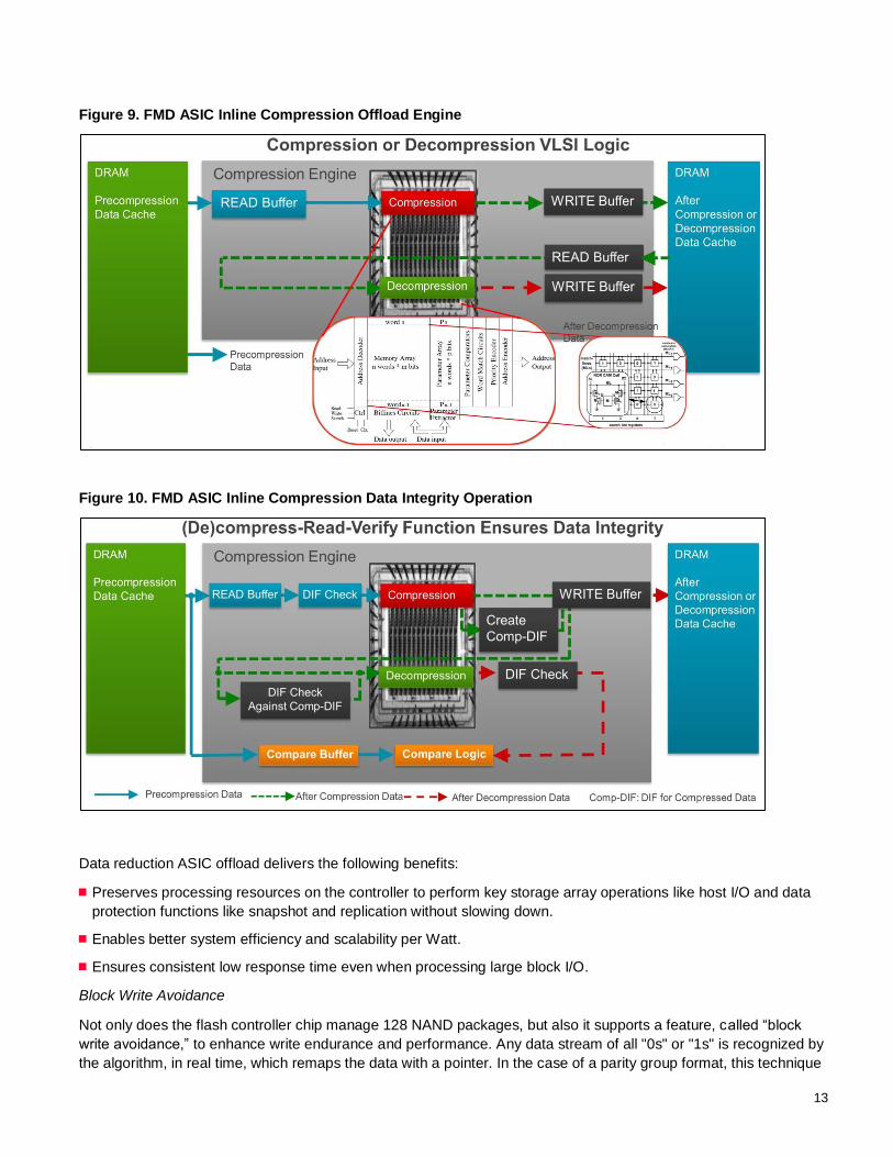
Inline Compression Offload
The ASIC also features a new “always on” inline compression offload engine. It is a very-large-scale integration
(VLSI) engine (see Figure 9) that enables lossless compression based on a derivative of the LZ77 sliding-window
algorithm. The encoding is designed for high performance, using a small-memory footprint. It ensures T10 data
integrity with (de)compress-read-verify function after compression and rehydration is completed (see Figure 10). Its
parallel processing delivers real-time (de)compression using a systolic array-content addressable memory
architecture, which ensures there is higher throughput, better efficiency and no lag that can create response time
spike. The compression engine enables similar data reduction efficiency to the software compression algorithms
found in other all flash arrays such as LZ4, LZ0, iGzip, zlib. The difference is that the FMD engine performs at 10
times the speed of other implementations because it is run on the FMD, eliminating the storage array burden
associated with typical software implementations on Intel core and/or journal-based file systems.
Flash Acceleration Offload
The compression engine enables similar data reduction efficiency to the software compression algorithms found in other all-flash arrays, such as LZ4, LZ0, iGzip or zlib. The difference is that the FMD engine performs at 10 times the speed of other implementations.
13
Figure 9. FMD ASIC Inline Compression Offload Engine
Figure 10. FMD ASIC Inline Compression Data Integrity Operation
Data reduction ASIC offload delivers the following benefits:
Preserves processing resources on the controller to perform key storage array operations like host I/O and data
protection functions like snapshot and replication without slowing down.
Enables better system efficiency and scalability per Watt.
Ensures consistent low response time even when processing large block I/O.
Block Write Avoidance
Not only does the flash controller chip manage 128 NAND packages, but also it supports a feature, called “block
write avoidance,” to enhance write endurance and performance. Any data stream of all "0s" or "1s" is recognized by
the algorithm, in real time, which remaps the data with a pointer. In the case of a parity group format, this technique

14
can deliver up to a 94% savings in storage space. A beneficial side effect of this space savings is to effectively
increase the overprovisioned area. This extra overprovisioning results in more efficiently run background tasks such
as garbage collection and wear leveling and, most importantly, an improvement in the sustained write performance.
This feature not only drastically reduces format times, but also, by eliminating unnecessary write and erase cycles,
it extends the effective life of the flash memory.
Workload Priority Access
This embedded flash controller feature integrates with SVOS RF, it is built on a multiqueue process, consistent
share of channel to the NAND package. NAND chip resources are preserved for application workload when
contention occurs (see Figure 11).
Figure 11. Workload Priority Access Feature
Smarter Garbage Collection
Smarter garbage collection also reduces NAND chip tasks load by enabling a block redistribution across multi-
NAND targets (see Figure 12). This feature improves response time consistency and reduces I/O latency from
background tasks that can create spikes in response times.

15
Figure 12. FMD Smarter Garbage Collection Tasks
VMware vSphere End-to-End Quality of Service
With the new workload priority feature and SVOS RF’s VASA provider with VMware vSphere Virtual Volumes
(VVols) and Storage I/O Control, VSP family systems can ensure end-to-end application workload quality of service
or QoS (see Figure 13). QoS is assured from a virtual machine down to an individual NAND flash package or die,
over typical flash background tasks such as garbage collection and data refresh.
Figure 13. FMD End-To-End Quality of Service
Flash Module DC2, FMD HD and FMD HDE Feature Highlights
Write Cliff
The degradation of I/O processing when managing housekeeping tasks and/or when under heavy write workloads
is a common occurrence with many flash controllers. Essentially, this degradation is an issue of processor schedule
handling, where housekeeping tasks such as garbage collection and wear-leveling demands cause a block in the

16
host I/O. Simply put, it is a symptom of a controller that does not have sufficient processor power to gracefully
handle sustained high-performance write environments.
The write cliff is not a concern with the FMD, which bypasses the housekeeping tasks from the I/O path. This
approach is possible thanks to use of a quad-core processor that has more than sufficient processing power.
Wear Leveling
Flash has a limited lifespan. An important characteristic of flash memory is that each write or erase cycle stresses
the cell, causing a deterioration of the cell over time. Compounding this fact is the probability of an imbalance or a
bias in cell activity, which creates an irregular distribution of these unstable cells.
Resident within the FMD is the necessary intelligence to minimize these challenges and to optimize the life of the
NAND flash. The FMD controller monitors the rate of writes, erasures and refreshes to eliminate biased activity by
balancing the rate of deterioration in the flash memory blocks. It then manages the physical data location with the
best match between the I/O frequency on the data and the NAND flash block usage status.
This durability enhancement is achieved with wear-leveling management and is key in extending the useful lifetime
of the NAND flash that populates the FMD.
Reliability Availability Serviceability (RAS)
To deliver the highest level of fault tolerance and provide a worry-free customer experience, the FMD DC2, FMD
HD and FMD HDE include numerous RAS functions that are tightly integrated with SVOS RF and the overall VSP
architecture.
Specific to data integrity, the FMD leverages multiple layers of ECC error checking to ensure that data is written
correctly and accurately preserved over time. The first level of ECC is done per transaction and provides end-to-end
error checking through a custom eight bytes DIF appended to write I/O recorded on the FMD DC2 and FMD HD
(see Figure 14).
To preserve the integrity of data writes, 112 bytes of ECC are appended for every 2KB of compressed data written.
This action translates to each FMD’s ECC being able to correct up to 59 bits per 2KB, which exceeds the standard
spec of 40 bits per 1.1KB of data. It ensures that even if a bit error is discovered, it can be easily recovered.
Subsequent read I/Os are processed via a 112 bytes of ECC per 2KB compressed logical page on the FMD DC2 to
confirm the integrity of the data.
Figure 14. FMD Error-Correcting Code

17
As data is written and read, the system monitors key metrics about the hardware and NAND. For instance, wear
levels are monitored, and when a NAND reaches 95% of its wear limit, we trigger an alarm. At 99% of the wear limit
we trigger a sparing alert. These alerts can be used by the local administrator or the Hitachi customer support, via
Hi-Track Remote Monitoring system reporting, to schedule a service activity before a failure occurs.
Power Loss Protection
The FMD includes a power loss protection (PLP) feature that protects data in storage devices against sudden
power loss. During FMD operation, data is temporarily stored in the DRAM cache memory in the drive to reduce the
performance gap between the host interface and the NAND flash package. Under normal operation, ongoing data
destaging from the DRAM to the NAND flash memory updates the latest metadata and user data to ensure data
integrity. In cases of unexpected sudden power loss, such as unplugging the power to the system without prior
notification, unexpected power outages, or unplugging devices from the system, the destaging process cannot be
completed and, depending on the type of cached data in the DRAM memory, sudden power loss can cause serious
device failure. Therefore, PLP feature is a way to create more time for the data destaging process under sudden
power-off situations by using dedicated capacitor backup. The capacitor is charged during power-on timeframes
and offers charged power to the FMD DC2 circuit when external power is off so that the data flush can be
completed.
Adaptive Data Refresh
To catch bit errors quickly, the FMD will perform what is called a high frequency "adaptive" data refresh. This
refresh is where the controller reads and recalculates the internal ECC on the entire FMD every two days and
dynamically optimizes page refresh based on applied error correction. Note: To secure the integrity of previously
written data, all data is rewritten at least every 30 days. This practice is key not only to extending flash cell longevity
but also to improving the overall sustained performance.
Periodic Data Diagnosis or Recovery
A uniquely powerful integration of features occurs when HAF is used with one of the supported Hitachi storage
systems. The data diagnostic and read retry functions of the FMD are partnered with the periodic data diagnostic
and recovery functions resident within Hitachi storage controllers. Smart protection with built-in monitoring detects
and reports reliability indicators to anticipate device failures. It uses processing lull to communicate read test logs
and errors every ~6 hours to SVOS RF; uncorrectable page will be rebuilding in the background asynchronously. If
the bit errors exceed the ECC correction capability of the FMD, then the data is read out by the read retry function.
This function adjusts the parameters of the flash memory and reads the data. The area is then refreshed, meaning
that the data is read and copied to a different area before the data becomes unreadable.
Data-at-Rest Encryption
Supported on the Virtual Storage Platform G1500 and VSP F1500 models, the FMD HDE allows the administrator to encrypt data at rest, with compression, without performance impact. By allowing organizations to encrypt at the bottom of the stack, we do not introduce latency at the application layer. This approach protects against threat models without having to alter critical upstream data that could affect performance. Organizations have a choice of third-party multivendor key management (KMIP) support, so there is no vendor lock in.
High-Speed Formatting
The formatting is done autonomously in the FMD. This highly efficient process is completed in approximately five
minutes, regardless of the number of drives to format. When compared to the 280 minutes that a similarly
configured array of SSDs (22.4TB) would take, it is apparent that systems employing the FMD have a reduced
install time.

18
Data Eradication
Hitachi offers a data eradication service that will physically erase all the user data on the device, including any bad
blocks and the overprovisioning of spaces. After the eradication is done, every cell in the FMD DC2 and/or FMD HD
is read to ensure that the eradication was completed successfully. The device data, such as wear leveling, is not
eradicated, so it can continue to be used and the remaining warranty period is preserved. The service exceeds
standards for U.S. National Institute of Standards and Technology (NIST) for data shredding. FMD HDE completes
a full cryptographic erasure (media sanitization) of any data on the drive when an internal encrypted drive is
removed from the storage system.
Conclusion
IT departments have finite budgets. Thus, cost along with robustness have been the primary constraints that have
limited a wider adoption of solid-state storage, particularly in the data center.
With these concerns in mind, Hitachi perceived the following challenges: How can we provide an enterprise-class,
high-performance, robust, flash-based storage option that is highly resilient? And, how do we do so cost-effectively?
The Hitachi team's answer was to create a purpose-built flash controller and all-flash storage virtualization operating
system that exploits the attractively priced NAND technology. The value added from integrating our Hitachi
Accelerated Flash, SVOS RF with the unique FMD-embedded controller delivers the performance, functionality,
robustness and endurance expected in an enterprise-class solution.
Appendix: External References
Hitachi IT Platform Division Group Engineering and Product Specifications.
Intel, Solid-State Drive DC S3610 Series Product Specifications, March 2015.
HGST, Ultrastar, 2.5-Inch Serial-Attached SCSI (SAS) Solid-State Drive Product Manual, June 2015.
Samsung, Application Note, Power loss protection, 2014.
Toshiba, PX02SM Series Enterprise Mid Endurance SSD Product Manual.
Samsung, SM1635 SSD Datasheet.
Crystal Forest Platform: Intel Communications Chipset 8900 to 8920 Series Performance Brief, January 2014.
IBM Real-Time Compression in IBM® SAN Volume Controller and IBM Storwize® V7000.
IBM Introducing and Implementing IBM® FlashSystem™ V9000.
Intel, High-Performance DEFLATE Compression on Intel Architecture Processors.
GitHub.com compression benchmark results.
Ren-Yang Yang and Chen-Yi Lee, High-Throughput Data Compressor Designs Using Content-Addressable
Memory, National Chiao Tung University.
Shih-Arn Hwang and Cheng-Wen Wu, Unified VLSI Systolic Array Design for LZ Data.
Compression, IEEE.
Micron, NAND Flash Memory –128Gb, 256Gb, 512Gb, 1Tb, 2Tb, Async/Sync, MLC Datasheet.
Micron, Ryan Fisher, Optimizing NAND Flash Performance, Flash Memory Summit 2008.
Nitin Agrawal, Vijayan Prabhakaran, Ted Wobber, John D. Davis, Mark Manasse, Rina Panigrahy, Design
Tradeoffs for SSD Performance.
Tim Canepa, Seagate, Flash Component Division, Anatomy of a high-performance hierarchical FTL Architecture;
Flash Memory Summit 2015.

Hitachi Vantara
Corporate Headquarters Contact Information
2845 Lafayette Street USA: 1-800-446-0744
Santa Clara, CA 95050-2639 USA Global: 1-858-547-4526
www.HitachiVantara.com | community.HitachiVantara.com HitachiVantara.com/contact HITACHI is a trademark or registered trademark of Hitachi, Ltd. VSP and Hi-Track are trademarks or registered trademarks of Hitachi Vantara. IBM, Storwize and FlashSystem are trademarks or registered trademarks of International Business Machines Corporation. All other trademarks, service marks and company names are
properties of their respective owners. WP-470-K I. Clatworthy September 2018.