
Science at the interface : grain boundaries in nanocrystalline metals
Upload
khangminh22Category
view
1download
0
J. Appl. Phys. 119, 235303 (2016); https://doi.org/10.1063/1.4954002 119, 235303
© 2016 Author(s).
Highly conductive grain boundaries incopper oxide thin filmsCite as: J. Appl. Phys. 119, 235303 (2016); https://doi.org/10.1063/1.4954002Submitted: 23 March 2016 • Accepted: 02 June 2016 • Published Online: 16 June 2016
Jonas Deuermeier, Hans F. Wardenga, Jan Morasch, et al.
ARTICLES YOU MAY BE INTERESTED IN
Visualization of nanocrystalline CuO in the grain boundaries of Cu2O thin films and effect on
band bending and film resistivityAPL Materials 6, 096103 (2018); https://doi.org/10.1063/1.5042046
Synthesis of Cu2O from CuO thin films: Optical and electrical properties
AIP Advances 5, 047143 (2015); https://doi.org/10.1063/1.4919323
Thin-film transistors based on p-type thin films produced at room temperature
Applied Physics Letters 96, 192102 (2010); https://doi.org/10.1063/1.3428434

Highly conductive grain boundaries in copper oxide thin films
Jonas Deuermeier,1,2,a) Hans F. Wardenga,2 Jan Morasch,2 Sebastian Siol,2,b)
Suman Nandy,1 Tom�as Calmeiro,1 Rodrigo Martins,1 Andreas Klein,2,c)
and Elvira Fortunato1
1Department of Materials Science, Faculty of Science and Technology, i3N/CENIMAT, Universidade NOVAde Lisboa and CEMOP/UNINOVA, Campus de Caparica, 2829-516 Caparica, Portugal2Department of Materials and Earth Sciences, Technische Universit€at Darmstadt, Jovanka-Bontschits-Straße2, D-64287 Darmstadt, Germany
(Received 23 March 2016; accepted 2 June 2016; published online 16 June 2016)
High conductivity in the off-state and low field-effect mobility compared to bulk properties is widely
observed in the p-type thin-film transistors of Cu2O, especially when processed at moderate tempera-
ture. This work presents results from in situ conductance measurements at thicknesses from sub-nm
to around 250 nm with parallel X-ray photoelectron spectroscopy. An enhanced conductivity at low
thickness is explained by the occurrence of Cu(II), which is segregated in the grain boundary and
locally causes a conductivity similar to CuO, although the surface of the thick film has Cu2O stoichi-
ometry. Since grains grow with an increasing film thickness, the effect of an apparent oxygen excess
is most pronounced in vicinity to the substrate interface. Electrical properties of Cu2O grains are at
least partially short-circuited by this effect. The study focuses on properties inherent to copper oxide,
although interface effects cannot be ruled out. This non-destructive, bottom-up analysis reveals phe-
nomena which are commonly not observable after device fabrication, but clearly dominate electrical
properties of polycrystalline thin films. Published by AIP Publishing.[http://dx.doi.org/10.1063/1.4954002]
I. INTRODUCTION
A significant economic potential lies within low-
temperature fabrication of transparent oxide electronics.1 A
successful commercialization is primarily held back by the
development of a complementary p-type transistor element.
With a band gap of 2.17 eV,2 Cu2O is one of the candidate p-
type materials, but shows a pronounced discrepancy between
bulk electrical properties and device behavior. Deposition by
reactive magnetron sputtering at room temperature results in
a Hall mobility of 1 cm2 V�1 s�1, however additional anneal-
ing at 200 �C for 1 h in air increases the mobility to 32 cm2
V�1 s�1 (own data, similar to results from the literature3,4).
In contrast, bottom-gated thin-film transistors (TFTs), pro-
duced at temperatures up to 200 �C, show field-effect mobili-
ties in the order of 10�3 cm2 V�1 s�1.5,6 A higher annealing
temperature above 500 �C (Refs. 7–9) is typically needed for a
field-effect mobility closer to the bulk value. This is com-
monly related to an increased grain size. An estimation of
sub-gap density of states close to the valence band maximum
in a Cu2O transistor annealed at 800 �C has resulted in a value
an order of magnitude higher than that of amorphous silicon
or organic TFTs.10 However, the intermediate temperature
approach (below 200–300 �C) has been shown to be feasible
by an adequate choice of bottom-gate dielectric substrate ma-
terial, leading to field-effect mobilities of 2 cm2 V�1 s�1 on
AlN and 0.5 cm2 V�1 s�1 on SrTiO3.11,12
Already one year after the first report on epitaxial
Cu2O as active channel in a TFT,13 the interpretation of
bulk properties has led to the conclusion that the low on-
off current ratio and the low field-effect mobility can be
either due to a secondary phase of CuO or ionization of
intrinsic donors (oxygen vacancy).14 In the case of high-
quality epitaxial films, such defects have to be localized at
interfaces and/or surfaces. Apart from a well known sur-
face oxidation of Cu(I) in Cu2O to Cu(II),15 a porosity of
Cu2O and an interdiffused layer due to high temperature
processing have been discussed to be the reasons for bad
transport properties at the interface between the polycrys-
talline Cu2O and the dielectric substrate.16,17 In the here
presented study, a surface oxidation is excluded as the elec-
trical analysis was entirely conducted in an ultra-high vac-
uum (UHV).
Cu2O has been reported to exist in non-stoichiometric
form, both polycrystalline and monocrystalline, when
quenched from high temperatures.18,19 At room temperature
and in ambient air, Cu2O is thermodynamically unstable, but
the eutectoid decomposition into Cu and CuO below 375 �Cis kinetically hindered.20 A structural stabilization has been
reported by (110) stacking faults in minerals of Cu2O, which
are understood as a missing plane of copper ions and give
rise to a formal increase in copper valency of the adjacent
cations.21 Grain boundaries, in general, have been shown to
present regions of an increased conductivity with respect to
monocrystalline material22 and act as a sink for intrinsic
defects.23 Apart from segregation of intrinsic defects, inho-
mogeneity may also exist in the form of oxidation states dif-
ferent from the parent material. In Cu2O, precipitate phases
containing either Cu(0) or Cu(II) might be present.20 Cu(0)
is metallic and forms a Schottky barrier to Cu2O.24 Cu(II)
occurs in another stable p-type oxide, CuO, which generally
exhibits a higher charge carrier concentration and lower Hall
a)Electronic mail: [email protected])Present address: National Renewable Energy Laboratory, Golden, Colorado
80401, USA.c)Electronic mail: [email protected]
0021-8979/2016/119(23)/235303/8/$30.00 Published by AIP Publishing.119, 235303-1
JOURNAL OF APPLIED PHYSICS 119, 235303 (2016)

mobility than Cu2O.25–27 This is due to the partial Cu 3d9
occupancy, which subjects the hole state to strong antiferro-
magnetic coupling.28 The higher carrier concentration is also
related to the Cu 3d9 configuration, since it introduces strong
electron-electron coupling to the valence band, which shifts
its maximum closer towards the Fermi energy.29 The value
of the band gap is approximately 1.5 eV.30
In order to describe the morphology of a film grown
from the vapor phase, a structure zone model has been devel-
oped.31 When grown without substrate heating, grains have
fibrous structure, predominantly oriented orthogonal to the
substrate surface.3 The grain size in this direction is equal to
the film thickness d, which is related to the lateral extension
of the grains L according to Equation (1).32 The exponent nmediates the curvature of the grain faces
d / Ln: (1)
Inhomogeneous electrical properties in polycrystalline semi-
conductors most commonly exist in the form of poorly con-
ductive, thin intergranular regions, with respect to the grains.
Consequently, most of the literature on electrical properties
of inhomogeneous semiconductors focuses on this case.33–35
A rather simple model, which accounts for highly conductive
grain boundaries, has been developed for polycrystalline
CeO2 on SiO2, growing with columnar morphology. In this
contribution, a similar model is used to correlate thickness-
dependent conductance data for Cu2O with the morphology
of the material. In parallel, changes in the copper oxidation
state are studied to reveal the origin of the inhomogeneous
electrical properties.
II. EXPERIMENTAL
Sample preparation for in situ X-ray photoelectron spec-
troscopy (XPS) was done at the DArmstadt Integrated
SYstem for MATerial research (DAISY-MAT), a cluster tool
which provides UHV transfer between deposition and charac-
terization chambers.36 Cu2O thin films where grown by reac-
tive radio frequency (RF) magnetron sputtering without
substrate heating. A 2 in. metallic copper target of 99.999%
purity purchased from Lesker was sputtered at 25 W (2.53 W
in.�2) and 0.5 Pa total pressure. Similar to earlier studies,37
the stoichiometry of Cu2O was optimized by adjusting the gas
flow ratio of oxygen with respect to the total gas flow in the
range of 3.7%–4.3%. This value had been found to depend on
target consumption. Figures of merit for optimized deposition
conditions were stoichiometry, obtained from areal peak
intensities divided by atomic sensitivity factors provided for
the instrument,38 the absence of the Cu 2 p satellite structure
of Cu(II),39 and a Fermi energy EF � EVB� 0.3 eV. Fermi
energies of 0.5–0.6 eV were found a more sensitive indicator
for small amounts of Cu(0) than the Cu LMM Auger emis-
sion.40 LMM refers to the orbitals in X-ray level notations,
which are involved in the Auger emission, more precisely
L3M4,5M4,5. Comparatively high Fermi energies in Cu2O can
be related to a depletion by the formation of Schottky barriers
to nanocrystalline copper precipitates.41,42 Samples of CuO
were grown with similar condition, but using an oxygen gas
flow ratio of 10%.
As substrates, SiO2 quartz glass, Al2O3 and Bi2O3 were
used. The quartz glass substrates had been provided by
CrysTec. Al2O3 was deposited by an atomic layer deposition
(ALD) in a home-made chamber at 200 �C substrate temper-
ature. The complete process is described elsewhere.43 In
addition, Al2O3 incorporated in a bottom-gate stack of a
multi-layer structure of Al2O3 and TiO2 by ALD (250 nm)
on sputter-deposited indium tin oxide (ITO, 160 nm) was
used as substrate. In the following, this substrate is referred
to as ATO. The dielectric surface and the interface to ITO
consist of 25 nm pure Al2O3. Planar Systems (now Beneq)
provided these substrates, which are used for the fabrication
of p-type oxide TFTs, as reported in the literature.5,12,44,45
Bi2O3 was reactively sputtered from a 2 in. metallic Bi target
provided by Alineason Materials Technology at 15 W (RF,
1.52 W in.�2) without substrate heating. A gas flow ratio of
10% oxygen was maintained at 0.5 Pa total pressure. Bi2O3
is an interesting material due to its high dielectric constant of
approximately 40, which has been studied previously in the
system.46,47
XPS was performed in a Physical Electronics PHI 5700
multi-technique surface analysis unit, using monochromatic
Al Ka radiation with an energy of 1486.6 eV, a take-off
angle (TOA) of 45�, and a pass energy of 5.85 eV, resulting
in an overall energy resolution of less than 0.4 eV. The sys-
tem is equipped with an electron flood gun for charge com-
pensation. In situ measurements of conductance G were
realized by connecting a Keithley 6487 picoammeter/voltage
source to the sample through two electrical feedthroughs in-
stalled on the XPS chamber. The substrate had been prepared
with two sputter-deposited gold electrodes in planar geome-
try. The width w and the length l of the measured sample
area were in the range of 6.5–8.3 cm and 1.2–1.3 cm, respec-
tively. The ohmic contact to both electrodes was confirmed
by current-voltage sweeps. As the measured currents have
been in the range of picoampere especially at low thickness,
the conductance was determined by applying a constant volt-
age of 1 V until the current reached a steady state. Then, the
voltage bias was set to zero and the current was read again
until steady state was reached. The difference of both steady-
state currents was used for calculation of the conductance.
The amount of voltage was chosen as compromise between
high signal-to-noise ratio of the measurement and little cur-
rent stress on the thin film.
The in situ XPS and IV characterization was done on
Cu2O films deposited onto plane quartz glass and onto quartz
glass coated either with 25 nm Al2O3 or 45 nm Bi2O3.
Furthermore, ATO was investigated in two runs. One of the
ATO runs involved an additional cleaning step by heating
the substrate in 0.5 Pa oxygen at 200 �C for 2 h immediately
before film deposition. Then, two substrates of ATO coated
with additional 45 nm Bi2O3 were studied in two separate
runs. With respect to deposition parameters, both runs were
identical.
The quartz substrate showed rather pronounced charging
during XPS measurement, which was partially compensated
by the electron flood gun. For the analysis of the films on
quartz glass coated with Al2O3 and Bi2O3, a second quartz
substrate was sputter-coated with an additional gold layer
235303-2 Deuermeier et al. J. Appl. Phys. 119, 235303 (2016)
prior to the respective deposition of Al2O3 and Bi2O3, which
was added on the same sample holder next to the insulating
substrate. While the insulating substrate served for conduct-
ance measurement, the conductive substrate was used for
XPS analysis. In this way, the use of the electron flood gun
could be avoided. The ATO substrates were subjected to less
pronounced charging, so they did not require the use of
charge compensation to obtain the spectra, however disre-
garding binding energies. In any case, charging disappeared
as soon as a sufficiently thick Cu2O film had been deposited.
An Asylum Research MFP-3D atomic force microscope
(AFM) was used to obtain surface roughnesses and average
grain sizes at the surface, as well as current maps in contact
mode with a voltage of 2 V applied to the tip (Asylum
Research PPP-CONTPt). Scanning electron microscopy
(SEM) was done with a Carl Zeiss Auriga. To obtain cross-
sectional images of the films, the samples had been manually
broken prior to measurement. The Hall effect was measured
with a custom Hall effect system48 as well as with a commer-
cial BioRad HL5550. X-ray diffraction (XRD) measure-
ments were done with a PANalytical X’Pert Pro
Diffractometer in Bragg-Brentano geometry. Film thickness
was measured by profilometry and the deposition rate was
assumed to be independent on film thickness.
III. RESULTS
A. Electrical film properties
The different types of insulating substrates investigated
in this study are referred to by the names as shown in Table
I. Stoichiometry, Fermi energy and in situ conductivity rfrom planar geometry of thick Cu2O and CuO are reported.
The conductivity is calculated according to Equation (2),
where Y is the reduced conductance, corrected for the elec-
trode geometry
r ¼ l
w
G
d¼ Y
d: (2)
The film thickness of the samples listed in Table I was gener-
ally 254 nm, except for sample ATO (1) (42 nm) and for
CuO on ATO (366 nm). All surfaces of thick Cu2O films are
stoichiometric within an error of 5%. Accordingly, they were
free of the characteristic spectral features described in Sec.
II, which indicates the absence of Cu(0) and Cu(II).
However, the conductivities at 254 nm film thickness are
quite different according to the type of substrate. Cu2O on
quartz shows the lowest value, followed by the Al2O3 sub-
strates. The low conductivity on quartz is not due to a mea-
surement artifact, since a similarly low value was obtained
on a sapphire substrate (not shown here). The highest con-
ductivities in Cu2O are obtained on Bi2O3 with further
increase when deposited on ATO/Bi2O3. In CuO, the con-
ductivity is comparatively high in accordance with the low
Fermi energy. The remainder of this article is concerned
with the wide range of conductivities observed in Cu2O by
evaluating the data with respect to film thickness.
Figure 1 shows the change in reduced conductance with
an increasing copper oxide thickness on a linear scale and in
double-logarithmic representation. The value of Y before any
film deposition is at least five orders of magnitude lower
than the final reduced conductance for all experiments. As
the measurements were performed in the vacuum system
directly after deposition, this observation is related to the
film properties and not to an extrinsic surface effect, which
may be caused, for example, by adsorbates. The most strik-
ing observation from Figs. 1(a)–1(c) is the strong initial
increase of conductance at thicknesses below 10 nm, com-
pared to the slope at higher thicknesses. This is found both
for Cu2O and CuO. Figs. 1(d) and 1(e) reveal the different
thicknesses, at which the onset of conduction occurs. The
root mean square (RMS) roughness of ATO-based substrates
is about 5 nm, which explains the observed higher conduc-
tion onset thickness compared to q/Al2O3 and q/Bi2O3. The
quartz-based substrates have a similar RMS roughness of
0.4 nm. The reason for the relatively high onset thickness on
quartz compared to q/Al2O3 and q/Bi2O3 is therefore sup-
posed to be related to a different substrate-film interaction.
In Figure 1(f), it is noteworthy, that for thicknesses below
5 nm, the conductance of Cu2O is nearly identical to CuO.
B. XPS analysis
Depending on film thickness, systematic changes in Cu
2p3=2 satellite intensity from the Cu2O films could be identi-
fied by XPS. Figure 2 shows the Cu 2p3=2 spectra of all
Cu2O thicknesses on q/Al2O3 as representative example. In
order to obtain a semi-quantification of the relative amount
of satellite emission with respect to film thickness, the fol-
lowing procedure was applied to each experiment: The back-
ground was removed according to the method of Shirley in
the binding energy range of Cu 2p3=2 including the satellite
region (around 927 eV–948.5 eV). Then, the areal intensity
of this region was calculated, and the spectra were normal-
ized to the respective area. The difference between the spec-
tra of each thickness and of the final film was then calculated
and integrated in the region, where Cu 2p3=2 satellites typi-
cally appear (around 938.3 eV–945.8 eV). The relative satel-
lite sensitivity of Cu2O is zero by definition and around 0.3,
when calculated for CuO.
The relative intensity of the Cu 2p3=2 satellite emission
with respect to the main line intensity is plotted against
Cu2O film thickness in Figure 3(a). In order to compare the
data to the conductance results, the conductivity r is shown
in Figure 3(b). A general accordance of Cu(II) satellite
TABLE I. Stoichiometry, Fermi energy, and conductivity (estimated from
planar geometry).
Substrate Ratio Cu/O EF � EVB (eV) r (S cm�1� 10�3)
Quartz (q) 1.98 0.26 0.3
q/Al2O3 2.13 0.23 2.2
q/Bi2O3 1.93 0.24 4.4
ATO (1) 1.89 0.27 10.2
ATO (2) 1.99 0.33 3.4
ATO/Bi2O3 (1) 2.05 0.29 8.6
ATO/Bi2O3 (2) 2.05 0.28 15.3
CuO on ATO 0.86 0.06 166.6
235303-3 Deuermeier et al. J. Appl. Phys. 119, 235303 (2016)

intensity and conductivity is apparent. However, the maxi-
mum satellite intensity is generally observed at lower thick-
nesses than the maximum conductivity. Note that the
substrate ATO (1) had been heated at 200 �C in 0.5 Pa oxy-
gen for 2 h prior to film deposition. This additional surface
cleaning step may be the reason for the lower satellite inten-
sity compared to that of Cu2O on ATO (2). However, this
does not affect the film conductivity, which is similar for
both samples.
C. Morphology
There is obviously a relationship between the excess
conductivity and the Cu(II)-related satellite intensity,
observed at low and intermediate Cu2O thicknesses. In order
to investigate whether grain boundaries have an effect on
conductivity, the morphology of Cu2O is included into the
analysis. XRD has shown the material to be of
FIG. 1. In situ reduced conductance data are shown with respect to increasing copper oxide thickness (a)–(c) on linear and (d)–(f) on double-logarithmic scale.
The type of substrate is indicated, using the same nomenclature as in Table I. (c), (f) The data on CuO, in comparison to Cu2O on ATO (2). The values left of
the broken line correspond to the uncoated substrate (at arbitrary thickness).
FIG. 2. Spectra of the Cu 2p3=2 satellite region of copper oxide on q/Al2O3
are shown as example to illustrate the thickness-dependent amount of Cu(II)
satellite emission and the procedure for semi-quantification. The blue curve
is the spectrum after the final deposition step, which is supposed to represent
pure Cu2O. The dark brown to light brown curves are the spectra at interme-
diate thicknesses. The green curve represents data of CuO.
FIG. 3. (a) The relative amount of Cu 2p3=2 satellite emission is displayed
with respect to Cu2O film thickness. XPS data of intermediate film thick-
nesses on ATO (2) has been acquired only at a thickness of 2.8 nm. (b)
Conductivity with respect to Cu2O thickness as calculated from reduced
conductance data.
235303-4 Deuermeier et al. J. Appl. Phys. 119, 235303 (2016)

polycrystalline cuprite phase without preferential crystallo-
graphic orientation, similar to the previous work.37 No CuO
phase could be detected by XRD (not shown here). Cross-
sectional SEM images of Cu2O on corning glass and q/Al2O3
are displayed in Figure 4. A fibrous grain structure is found,
with a lateral grain size which increases with thickness.3
AFM topographies have been used to obtain a rough estimate
of the grain size at the surface after complete film deposition.
An average value of 35 6 15 nm was obtained, without sys-
tematic dependency on the substrate material.
Conductive atomic force microscopy (CAFM) was
measured to obtain direct evidence for an increased grain
boundary conductivity. The best results were obtained on a
100 nm thick sample deposited on ITO-coated glass in a
commercial stand-alone sputtering chamber by AJA
International. On these samples, Cu2O phase purity without
preferential crystallographic orientation was confirmed by
XRD and optical transmittance spectroscopy (not shown
here). Topography and current map are presented in Figure
5. The thin bright lines of increased current between the
grains are clear evidence for the increased grain boundary
conductivity.
IV. DISCUSSION
When the lateral grain size L increases with thickness
according to Equation (1), the volume fraction of grain boun-
daries decreases with increasing thickness. Consequently, if
a grain boundary effect is at play, enhanced conductance at
low thicknesses can only be explained by the existence of
more conductive grain boundaries with respect to the grain
interior. G€obel et al. have described the increase in grain
boundary conductance for the columnar morphology of their
samples by a model of cuboid grains of horizontal dimen-
sions L and a vertical extension equal to the film thickness
d.49 Grain boundaries perpendicular to the current flow are
neglected. The total reduced conductance Y with respect to
thickness is expressed as parallel connection of grain con-
ductance Ygrain and grain boundary conductance YGB
Y ¼ Ygrain þ YGB: (3)
The situation is illustrated in Figure 6(a). Figure 6(b) shows
a schematic representation of a film morphology with linear
cone faces (n¼ 1). Upon an increase in average grain size Lwith d, regions close to the substrate interface remain at
smaller L than regions close to the film surface. For this rea-
son, the total conductance needs to be integrated over
thickness
YðdÞ ¼ðd
0
r�ðzÞ dðzÞ: (4)
When dividing Y(d) by the film thickness d according to
Equation (2), an average value for conductivity of the inho-
mogeneous thin film is obtained. An expression for r*(z),
which satisfies the interpretation by G€obel et al., is given in
the following equation:
r� zð Þ ¼ rgrain
L zð ÞL zð Þ þW
þ rGB
W
L zð Þ þW; (5)
rGB and rgrain are the respective conductivities of grain
boundary and grain. The grain boundary width W is below a
nanometer, since it describes a rather highly doped region.49
Figures 7(a) and 7(b) show results from the model, calcu-
lated with W¼ 0.5 nm. In the calculation, the grains begin to
grow laterally only at a thickness of 1 nm, which is supposed
to account for an interface layer of high conductivity, equal
to rGB. The conductivity inside the grains is chosen equal to
monocrystalline Cu2O and the grain boundary conductivity
is within the range of typical values for CuO (0.01 S cm�1 as
single crystal and 1 S cm�1 as thin film, sputtered-deposited
at room temperature).25,26,30 All curves have been calculated
with rgrain¼ 10�6 S/cm and rGB¼ 0.1 S/cm. For compari-
son, Fig. 7(c) reproduces the measured conductivities on the
same scale. Due to the limited amount of data points at dif-
ferent thicknesses for each substrate material, a reliable fit-
ting of the data could not be conducted.
Fig. 7(a) illustrates the effect of different L(z) on the cal-
culated conductivity. Apart from of the linear relation
(n¼ 1), a square dependency (n¼ 2) in red and a cubic one
(n¼ 3) in gray are displayed. The more drastic the initial
increase in L, the stronger is the conductivity decay with
FIG. 4. Cross-sectional SEM images of Cu2O (a) on corning glass and (b)
on q/Al2O3.
FIG. 5. (a) Topography and (b) current map of Cu2O on ITO-coated glass.
FIG. 6. (a) The two parallel currents through the grain boundary (red) and
through the grains (blue) are illustrated, together with the respective conduc-
tances. (b) Schematic representation of the film morphology, where L is the
grain size, W is the width of the grain boundary, and d is the film thickness
along z.
235303-5 Deuermeier et al. J. Appl. Phys. 119, 235303 (2016)

increasing thickness. Fig. 7(b) shows that a similar change in
r can be obtained by considering an interface layer with con-
ductivity equal to rGB and a monocrystalline bulk material
of rgrain.
It is apparent from Figure 7 that thickness-dependent
analysis of conductance alone cannot distinguish whether an
enhanced conductivity at low thickness is due to an interface
or a grain boundary effect.49 For this reason, additional exper-
imental evidence needs to be considered. In the previous
study, conductivity measurements on CuO thin films of differ-
ent grain sizes with respect to temperature and atmosphere
revealed the existence of more conductive grain boundaries in
this material.30 In the light of the present discussion, this cor-
responds well to the initially enhanced conductivity in CuO
displayed in Figures 1(c) and 1(f). For bulk samples of Cu2O,
there is evidence in the literature to support the idea of the
increased grain boundary conductivity.22,23 The Hall effect
measurements on Cu2O thin films by Lee et al. confirm this,
although not discussed by the authors: As the average grain
size is reduced by two orders of magnitude, (1) carrier concen-
tration increases while mobility decreases up to the point that
no stable Hall voltage is obtained. Simultaneously, (2) the
concentration of ionized impurities increases, which dominate
charge carrier scattering at low temperature.3 An increasing
impurity concentration gradually changes the electrical prop-
erties of Cu2O to be rather similar to CuO. Given the possibil-
ity of highly conductive grain boundaries, a segregation of
defects in the grain boundary can correlate observation (1)
with observation (2). Consequently, grain boundaries are con-
cluded to be the cause for the increased conductivity at low
film thickness, as presented in this article. The results pre-
sented here show that XPS is able to detect the relevant
change in cation oxidation state to prove the existence of
Cu(II). The increased Cu(II)-related intensity at low film
thickness where grain size is expected to be relatively small
suggests that Cu(II) is present at the grain boundaries of
Cu2O. It is important for this assignment that the analysis is
carried out in dependence on thickness, non-destructively, and
in vacuum, which prevents surface oxidation.
The Cu2O films are apparently rich in oxygen at low
thickness, despite no sign for non-stoichiometry at high
thickness (see Table I). Under more reducing deposition con-
ditions, the formation of Cu(0) becomes more likely. The
width of the depletion layer, caused by the Cu/Cu2O
Schottky junction is 0.5–1 lm.24 In case Cu(0) segregates in
the grain boundaries, grains of similar size as in the present
study would be fully depleted and no thickness dependence
of conductivity could be observed by the here applied experi-
mental procedure.
Given that Cu(II) is present at the grain boundaries in
Cu2O thin films, the film may be approximated by Cu2O
grains separated by CuO grain boundary phases.
Transmission electron microscopy could confirm the exis-
tence of a CuO phase between Cu2O grains, however an insitu sample preparation procedure would be required to pre-
vent additional oxidation by exposure to ambient air, which
was not available. In case any CuO phase is formed, the
interface between Cu2O and CuO is important for determin-
ing the grain boundary properties. As a direct determination
of the energy band alignment between Cu2O and CuO is not
possible using photoemission, the corresponding alignment
is derived here using the transitivity rule according to DEVB
(Cu2O, CuO)¼UB (Cu2O, M)þUB (M, CuO). UB is the
Schottky barrier for holes at the corresponding interface. Mrepresents a common metal. This procedure has been suc-
cessfully applied to interfaces of semiconducting oxides.50,51
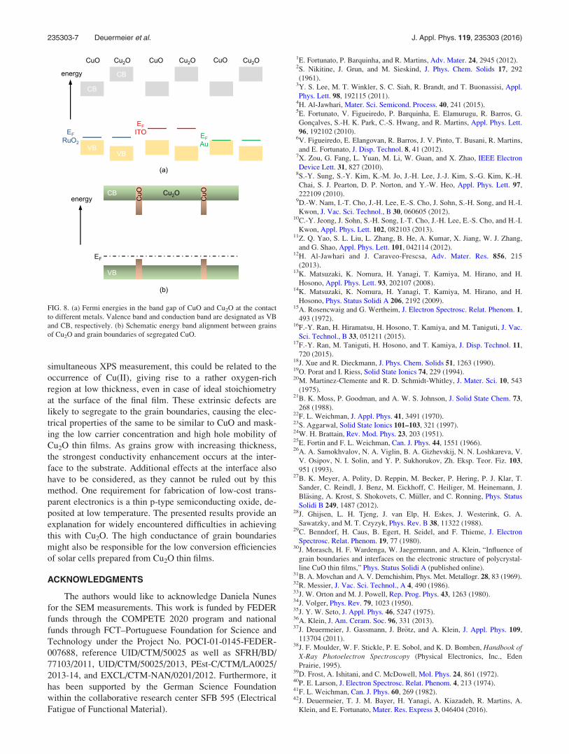
Figure 8(a) schematically shows Fermi energies in Cu2O and
CuO at the contacts to RuO2, ITO, and Au. The data have
been obtained by photoemission according to the method by
Kraut et al.52 and are partially taken from the previous stud-
ies.30,37,53 The valence band discontinuity between CuO and
Cu2O is 0.2 eV. In the case of a grain boundary segregation
of CuO in Cu2O, a schematic energy band alignment as
sketched in Figure 8(b) will occur. The higher valence band
maximum at the grain boundaries immediately explains the
higher carrier concentration and therefore the higher conduc-
tivity of the grain boundary.
V. CONCLUSION
The analysis of conductance with respect to film thick-
ness in UHV conditions has shown increased conductivity in
polycrystalline Cu2O thin films at low thicknesses. By
FIG. 7. Effective conductivity from calculation for different (a) grain
growth models L(z) and (b) interface layer thicknesses. The final grain size
of L¼ 40 nm is similar to the experimentally obtained values. (c)
Conductivities from the experiment are shown with the same symbol cod-
ing as in Figs. 1 and 3.
235303-6 Deuermeier et al. J. Appl. Phys. 119, 235303 (2016)
simultaneous XPS measurement, this could be related to the
occurrence of Cu(II), giving rise to a rather oxygen-rich
region at low thickness, even in case of ideal stoichiometry
at the surface of the final film. These extrinsic defects are
likely to segregate to the grain boundaries, causing the elec-
trical properties of the same to be similar to CuO and mask-
ing the low carrier concentration and high hole mobility of
Cu2O thin films. As grains grow with increasing thickness,
the strongest conductivity enhancement occurs at the inter-
face to the substrate. Additional effects at the interface also
have to be considered, as they cannot be ruled out by this
method. One requirement for fabrication of low-cost trans-
parent electronics is a thin p-type semiconducting oxide, de-
posited at low temperature. The presented results provide an
explanation for widely encountered difficulties in achieving
this with Cu2O. The high conductance of grain boundaries
might also be responsible for the low conversion efficiencies
of solar cells prepared from Cu2O thin films.
ACKNOWLEDGMENTS
The authors would like to acknowledge Daniela Nunes
for the SEM measurements. This work is funded by FEDER
funds through the COMPETE 2020 program and national
funds through FCT–Portuguese Foundation for Science and
Technology under the Project No. POCI-01-0145-FEDER-
007688, reference UID/CTM/50025 as well as SFRH/BD/
77103/2011, UID/CTM/50025/2013, PEst-C/CTM/LA0025/
2013-14, and EXCL/CTM-NAN/0201/2012. Furthermore, it
has been supported by the German Science Foundation
within the collaborative research center SFB 595 (Electrical
Fatigue of Functional Material).
1E. Fortunato, P. Barquinha, and R. Martins, Adv. Mater. 24, 2945 (2012).2S. Nikitine, J. Grun, and M. Sieskind, J. Phys. Chem. Solids 17, 292
(1961).3Y. S. Lee, M. T. Winkler, S. C. Siah, R. Brandt, and T. Buonassisi, Appl.
Phys. Lett. 98, 192115 (2011).4H. Al-Jawhari, Mater. Sci. Semicond. Process. 40, 241 (2015).5E. Fortunato, V. Figueiredo, P. Barquinha, E. Elamurugu, R. Barros, G.
Goncalves, S.-H. K. Park, C.-S. Hwang, and R. Martins, Appl. Phys. Lett.
96, 192102 (2010).6V. Figueiredo, E. Elangovan, R. Barros, J. V. Pinto, T. Busani, R. Martins,
and E. Fortunato, J. Disp. Technol. 8, 41 (2012).7X. Zou, G. Fang, L. Yuan, M. Li, W. Guan, and X. Zhao, IEEE Electron
Device Lett. 31, 827 (2010).8S.-Y. Sung, S.-Y. Kim, K.-M. Jo, J.-H. Lee, J.-J. Kim, S.-G. Kim, K.-H.
Chai, S. J. Pearton, D. P. Norton, and Y.-W. Heo, Appl. Phys. Lett. 97,
222109 (2010).9D.-W. Nam, I.-T. Cho, J.-H. Lee, E.-S. Cho, J. Sohn, S.-H. Song, and H.-I.
Kwon, J. Vac. Sci. Technol., B 30, 060605 (2012).10C.-Y. Jeong, J. Sohn, S.-H. Song, I.-T. Cho, J.-H. Lee, E.-S. Cho, and H.-I.
Kwon, Appl. Phys. Lett. 102, 082103 (2013).11Z. Q. Yao, S. L. Liu, L. Zhang, B. He, A. Kumar, X. Jiang, W. J. Zhang,
and G. Shao, Appl. Phys. Lett. 101, 042114 (2012).12H. Al-Jawhari and J. Caraveo-Frescsa, Adv. Mater. Res. 856, 215
(2013).13K. Matsuzaki, K. Nomura, H. Yanagi, T. Kamiya, M. Hirano, and H.
Hosono, Appl. Phys. Lett. 93, 202107 (2008).14K. Matsuzaki, K. Nomura, H. Yanagi, T. Kamiya, M. Hirano, and H.
Hosono, Phys. Status Solidi A 206, 2192 (2009).15A. Rosencwaig and G. Wertheim, J. Electron Spectrosc. Relat. Phenom. 1,
493 (1972).16F.-Y. Ran, H. Hiramatsu, H. Hosono, T. Kamiya, and M. Taniguti, J. Vac.
Sci. Technol., B 33, 051211 (2015).17F.-Y. Ran, M. Taniguti, H. Hosono, and T. Kamiya, J. Disp. Technol. 11,
720 (2015).18J. Xue and R. Dieckmann, J. Phys. Chem. Solids 51, 1263 (1990).19O. Porat and I. Riess, Solid State Ionics 74, 229 (1994).20M. Martinez-Clemente and R. D. Schmidt-Whitley, J. Mater. Sci. 10, 543
(1975).21B. K. Moss, P. Goodman, and A. W. S. Johnson, J. Solid State Chem. 73,
268 (1988).22F. L. Weichman, J. Appl. Phys. 41, 3491 (1970).23S. Aggarwal, Solid State Ionics 101–103, 321 (1997).24W. H. Brattain, Rev. Mod. Phys. 23, 203 (1951).25E. Fortin and F. L. Weichman, Can. J. Phys. 44, 1551 (1966).26A. A. Samokhvalov, N. A. Viglin, B. A. Gizhevskij, N. N. Loshkareva, V.
V. Osipov, N. I. Solin, and Y. P. Sukhorukov, Zh. Eksp. Teor. Fiz. 103,
951 (1993).27B. K. Meyer, A. Polity, D. Reppin, M. Becker, P. Hering, P. J. Klar, T.
Sander, C. Reindl, J. Benz, M. Eickhoff, C. Heiliger, M. Heinemann, J.
Bl€asing, A. Krost, S. Shokovets, C. M€uller, and C. Ronning, Phys. Status
Solidi B 249, 1487 (2012).28J. Ghijsen, L. H. Tjeng, J. van Elp, H. Eskes, J. Westerink, G. A.
Sawatzky, and M. T. Czyzyk, Phys. Rev. B 38, 11322 (1988).29C. Benndorf, H. Caus, B. Egert, H. Seidel, and F. Thieme, J. Electron
Spectrosc. Relat. Phenom. 19, 77 (1980).30J. Morasch, H. F. Wardenga, W. Jaegermann, and A. Klein, “Influence of
grain boundaries and interfaces on the electronic structure of polycrystal-
line CuO thin films,” Phys. Status Solidi A (published online).31B. A. Movchan and A. V. Demchishim, Phys. Met. Metallogr. 28, 83 (1969).32R. Messier, J. Vac. Sci. Technol., A 4, 490 (1986).33J. W. Orton and M. J. Powell, Rep. Prog. Phys. 43, 1263 (1980).34J. Volger, Phys. Rev. 79, 1023 (1950).35J. Y. W. Seto, J. Appl. Phys. 46, 5247 (1975).36A. Klein, J. Am. Ceram. Soc. 96, 331 (2013).37J. Deuermeier, J. Gassmann, J. Br€otz, and A. Klein, J. Appl. Phys. 109,
113704 (2011).38J. F. Moulder, W. F. Stickle, P. E. Sobol, and K. D. Bomben, Handbook of
X-Ray Photoelectron Spectroscopy (Physical Electronics, Inc., Eden
Prairie, 1995).39D. Frost, A. Ishitani, and C. McDowell, Mol. Phys. 24, 861 (1972).40P. E. Larson, J. Electron Spectrosc. Relat. Phenom. 4, 213 (1974).41F. L. Weichman, Can. J. Phys. 60, 269 (1982).42J. Deuermeier, T. J. M. Bayer, H. Yanagi, A. Kiazadeh, R. Martins, A.
Klein, and E. Fortunato, Mater. Res. Express 3, 046404 (2016).
FIG. 8. (a) Fermi energies in the band gap of CuO and Cu2O at the contact
to different metals. Valence band and conduction band are designated as VB
and CB, respectively. (b) Schematic energy band alignment between grains
of Cu2O and grain boundaries of segregated CuO.
235303-7 Deuermeier et al. J. Appl. Phys. 119, 235303 (2016)

43T. J. M. Bayer, A. Wachau, A. Fuchs, J. Deuermeier, and A. Klein, Chem.
Mater. 24, 4503 (2012).44E. Fortunato, V. Figueiredo, P. Barquinha, E. Elamurugu, R. Barros, G.
Goncalves, S.-H. K. Park, C.-S. Hwang, and R. Martins, Appl. Phys. Lett.
96, 239902 (2010).45Z. Wang, H. A. Al-Jawhari, P. K. Nayak, J. A. Caraveo-Frescas, N. Wei,
M. N. Hedhili, and H. N. Alshareef, Sci. Rep. 5, 9617 (2015).46S. Li, J. Morasch, A. Klein, C. Chirila, L. Pintilie, L. Jia, K. Ellmer, M.
Naderer, K. Reichmann, M. Gr€ating, and K. Albe, Phys. Rev. B 88,
045428 (2013).47J. Morasch, S. Li, J. Br€otz, W. Jaegermann, and A. Klein, Physica Status
Solidi A 211, 93 (2014).48M. V. Hohmann, A. Wachau, and A. Klein, Solid State Ionics 262, 636
(2014).
49M. C. G€obel, G. Gregori, X. Guo, and J. Maier, Phys. Chem. Chem. Phys.
12, 14351 (2010).50R. Schafranek, S. Li, F. Chen, W. Wu, and A. Klein, Phys. Rev. B 84,
045317 (2011).51S. Li, F. Chen, R. Schafranek, T. J. M. Bayer, K. Rachut, A. Fuchs, S. Siol,
M. Weidner, M. Hohmann, V. Pfeifer, J. Morasch, C. Ghinea, E. Arveux, R.
G€unzler, J. Gassmann, C. K€orber, Y. Gassenbauer, F. S€auberlich, G. V. Rao,
S. Payan, M. Maglione, C. Chirila, L. Pintilie, L. Jia, K. Ellmer, M. Naderer,
K. Reichmann, U. B€ottger, S. Schmelzer, R. C. Frunza, H. Ursic, B. Malic,
W.-B. Wu, P. Erhart, and A. Klein, Phys. Status Solidi RRL 8, 571 (2014).52J. R. Waldrop, W. Grant, S. P. Kowalczyk, and E. A. Kraut, J. Vac. Sci.
Technol., A 3, 835 (1985).53S. Siol, “Kupfer-Chalkogenide f€ur photovoltaische Anwendungen,” Ph.D.
thesis, Technische Universit€at Darmstadt, 2014.
235303-8 Deuermeier et al. J. Appl. Phys. 119, 235303 (2016)
This article may be downloaded for personal use only. Any other use requires prior permission of the author and AIP Publishing. This article appeared in Journal of Applied Physics 119, 235303 (2016) and may be found at https://doi.org/10.1063/1.4954002.
Available under only the rights of use according to UrhG.
Copyright © 2022 FDOKUMEN


![Kinetics of diffusion induced grain boundary migration of [100] twist boundaries in the Cu(Zn) system](https://static.fdokumen.com/doc/165x107/631c6051a906b217b906ec8b/kinetics-of-diffusion-induced-grain-boundary-migration-of-100-twist-boundaries.jpg)