Deformation-induced crystallization in amorphous Al85Ni10La5 alloy

Thin Solid Films 426(2003) 191–199
0040-6090/03/$ - see front matter� 2003 Elsevier Science B.V. All rights reserved.doi:10.1016/S0040-6090(03)00027-0
High temperature-induced crystallization in tantalum pentoxide layers andits influence on the electrical properties
E. Atanassova *, M. Kalitzova , G. Zollo , A. Paskaleva , A. Peeva , M. Georgieva , G. Vitalia, a b a a a b,1
Institute of Solid State Physics, Bulgarian Academy of Sciences, Tzarigradsko Chaussee 72, Sofia 1784, Bulgariaa
Department of Energetics, University ‘La Sapienza’ of Rome, A. Scarpa 14, Rome 00161, Italyb
Received 22 October 2002; received in revised form 23 October 2002; accepted 7 January 2003
Abstract
RF sputtered Ta O films(23–26 nm) on Si, before and after high temperature(873, 1123 K) O annealing have been2 5 2
investigated with respect to their dielectric and microstructural properties. Both high resolution transmission electron microscopy(HR-TEM) analysis and electrical measurements indicated the presence of extremely thin SiO at the interface with Si. The2
substrate temperature during deposition has no effect on the flatness of the SiO –Ta O interface but it affects the flatness of the2 2 5
Si–SiO interface—for films obtained on heated substrate, this interface becomes abrupt. The as-deposited and the annealed, at2
873 K, films are amorphous where as after 1123 K annealing, they crystallize in orthorhombic phase,(there is evidence that thecrystal phase electrically manifests as slow states). The crystallization of the films favor a larger dielectric constant at 1 MHz anda smaller leakage current especially in the dielectric voltage region, which will be the operating voltage for future technologygenerations. A leakage current of;10 Aycm at 1 V can be achieved. The results are discussed in terms of relative impact ofy9 2
two concurrent mechanisms during high temperature O treatment—an appearance of crystal phase and a real annealing of the2
films accompanied with an improvement of the dielectric properties.� 2003 Elsevier Science B.V. All rights reserved.
Keywords: Crystallization; TEM; MOS structure; Electrical properties and measurements
1. Introduction
Although a great success has been achieved, thecurrent Dynamic Random Access Memories(DRAMs)technology cannot be extended to the giga bit scale andbeyond because the number of challenges have to beovercome. The development of Ultra Large Scale Inte-gration(ULSI) storage capacitors for DRAM generationof 256 Mbit and higher requires alternative dielectricmaterials with a high dielectric constant. The mostpromising candidate for a very thin capacitor dielectricfilm in the future DRAMs is Ta O which might be2 5
utilized in the high density memories with an oxideequivalent thickness of approximately 5 nmw1–5x. Theintegration of Ta O in a complete device fabrication2 5
*Corresponding author. Tel.:q359-2-7144448; Fax:q359-2-975-3632.
E-mail address: [email protected](E. Atanassova).Present address: Forschungszentrum Rossendorf, PF 510119,1
Drezden D-01314, Germany.
process is still a subject of ongoing investigations.Several problems remain to be overcome before suffi-cient reliability can be provided in the ULSI fabrication.Among the points to be taken into consideration is theobserved crystallization of amorphous Ta O at relative-2 5
ly high temperatures()873 K) resulting in a changeof electrical properties and, in most cases, in a reductionof the breakdown strengthw2,6–10x. For the applicationof Ta O in high density DRAMs, however, the Ta O2 5 2 5
capacitor must be compatible with a high temperatureprocessing which is standard in the DRAMs fabrication.Since processing at temperatures greater than 873 K isroutinely used in manufacturing of ULSI circuits, theformation of amorphous film in the early stages oftechnology would result in a crystallization of this layerduring a typical processing sequence. Accordingly, theimplementation of these films is not compatible with aconventional silicon technology. On the other hand, theleakage current of thin as-fabricated Ta O layers is2 5
usually large and an appropriate annealing is needed toreduce this currentw4,5,11–15x. The leakage current
192 E. Atanassova et al. / Thin Solid Films 426 (2003) 191–199
density(one of the most important properties of Ta O2 5
based memory capacitor) is very sensitive to materialimperfections such as oxygen vacancies, which act toincrease the current leakage through the amorphousfilms. For crystallized films, the situation is more com-plicated due to grain boundary effects. Many researchershave studied the effect of a number of annealingtechniques, e.g. the use of dry O , ultra violet generated2
ozone and plasmas as well as various two step processesw1–4,13–15x. The interface may also have a large impacton the current through the capacitor, resulting in unpre-dictable leakage current properties of the devices. Mostof the studies on Ta O are limited to the film itself or2 5
at the film microstructure. Since the interfacial compo-sition and chemical states can have a strong influenceon the performance of the devices utilizing Ta O , it is2 5
critical to have a knowledge of the interface layer inorder to fully understand the relationship between thestructure and the film properties. During the formationof Ta O , an interfacial SiO layer is inevitably obtained2 5 2
at the Ta O –Si interface. The growth of this SiO is2 5 2
favored by an oxidizing ambient at the beginning orduring the deposition step and by post-fabrication treat-ments usually performed in an oxygen atmosphere torepair oxygen vacancies in Ta O . The formation of2 5
SiO raises the following issues for the Ta O –Si sys-2 2 5
tem: reduction of the global dielectric constant due tothe low dielectric constant of SiO ; modification of the2
conduction mechanism in the double structure; andimproved interfacial properties due to the high qualitySi–SiO interface.2
Recentlyw2,5,16–18x we have shown that amorphoustantalum oxide films with stoichiometric compositioncan be successfully obtained on Si by using RF sputter-ing process. The electrical measurements in a metal–oxide–silicon (MOS) configuration demonstrate animprovement of the electrical properties of the sputteredTa O on Si after dry O annealing. The results show2 5 2
that the amorphous state of the sputtered films ismaintained at an annealing temperature lower than 873K, whereas crystalline Ta O(orthorhombic b-Ta O2 5 2 5
phase) is obtained after oxygen annealing at 1123 K. Itwas also found that the dielectric constant criticallydepends on the appearance of crystalline phase in thelayers. We also have evidence that the post-depositionoxygen annealing at 1123 K is very effective formaintaining a large dielectric constant(up to 37) andfor a reduction of a fixed oxide charge(less than 1010
cm ) but the effect on the leakage current exhibits ay2
thickness dependence. That is why, a precise structuralanalysis is required for these films in order to clarifythe conditions under which the crystallization occurs inclose relation to the parameters of the fabricationprocess.
In the present paper, the effect of high temperaturepost-deposition annealing in dry O on the microstruc-2
ture and the electrical properties of relatively thin(23–26 nm) RF sputtered Ta O films on Si has been studied,2 5
paying special attention to the relationship between theleakage current characteristics and the crystalline struc-ture of the layers. This thickness region appears to bevery attractive for application in high density DRAMs.On the other hand, in the thinner oxides, the relativefraction of the structural non-perfections is expected toincrease which could manifest itself in a larger currentvalue. The role of the crystalline phase formed in theTa O layers after annealing on the insulating properties2 5
of the system Ta O –Si, and the structural features of2 5
the inevitably formed SiO layer at the interface with Si2
have been analyzed.
2. Experimental procedure
Chemically cleaned p-type(100) silicon wafers of15–17 Vcm resistivity were used as substrates forTa O films. Tantalum oxide was deposited by reactive2 5
sputtering of Ta target in a mixture of Ar and O gases;2
O content is 10%. Presputtering of the target was2
carried out in Ar. The total gas pressure of the gasmixture during the deposition was 0.33 Pa and RFpower density was 3.6 Wycm ; the deposition rate was2
5 nmymin and the target to substrate distance was 3.5cm. In a number of experiments the silicon substratewas not heated during the deposition and remained closeto a room temperature. In others, the substrate temper-ature,T was 493 K. After the deposition the sampless
were annealed in dry O at 873 or 1123 K for 30 min.2
The films microstructure was characterized by HR-TEM of cross-sectional specimens and a computer proc-essing of the corresponding TEM images(Philips 300electron microscope operating at 300 kV acceleratingvoltage and in seven beams bright field mode). HR-TEM specimens were prepared by a cleavage normallyto N110M direction of Si substrate using standard tech-niques for mechanical thinning and an ion beam etchingas a final thinningw19x. The HR-TEM images havebeen digitized and successively processed in the Fourierspacew20x. The reflection high energy electron diffrac-tion (RHEED) patterns were recorded in an EM 6GAEI electron microscope, equipped with a high resolu-tion stage for electron diffraction, at 60 kV accelerationvoltage. The incidence angle of the electron beam wasus0.88. In order to perform in-depth RHEED analysisthe specimens have been etched in 10% HF.
The electrical characterization of the films with athickness of 23–26 nm was carried out on MOS capac-itors with evaporated Al gate electrodes with differentgate areas in the range of(0.1–2.5)=10 cm . They3 2
oxide chargeQ was evaluated from high frequency(1f
MHz) capacitance voltage(C–V) curves. In order toobtain accurate information of permittivity of the layersand its dependence on the film thickness,C–V measure-

193E. Atanassova et al. / Thin Solid Films 426 (2003) 191–199
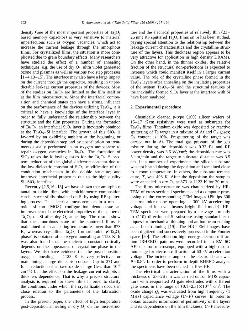
Fig. 1. HR-TEM micrograph in(110) projection:(a) as-deposited films,T s293 K; the steps at the Si–SiO interface are labeled with S. FFTs 2
of the image from the Si matrix is inserted in inset the figure:(b) as-deposited films,T s493 K; (c) 493 K films after oxygen annealing at 873s
K. FFT of the image obtained from Ta O layer is shown in the inset. The regions labeled with 1 and 2 correspond to the tendency of(001)2 5
Ta O spots formation.2 5
ments were made for layers with thickness in the rangeof 15–80 nm. The thicknessd and the refractive indexof the layers were measured by ellipsometry(ls632.8nm) and the dielectric constant́ of the layers waseff
determined from the capacitance valueC at accumula-o
tion using the measured values of the thickness. Rampedcurrent–voltage(I–V) characteristics with a ramp rateof 0.26 Vys were used to investigate the leakage currentat low voltages. The breakdown fieldE was definedbd
as the average applied field at which the current densitythrough the dielectric exceeds 4=10 Aycm .y4 2
3. Results and discussion
3.1. Structural analysis
HR-TEM image of the Ta O film deposited at room2 5
temperature(T s293 K) is presented in Fig. 1a,dss
23.5 nm. The(110) lattice image of the Si substrate isclearly seen in the lower part of the picture where(200)and two sets of(111) planes are detectable(d s111 Si
0.313 nm andd s0.271 nm). The digital power200 Si
spectrum,wi.e. the fast Fourier transform,(FFT)x of theSi matrix is shown in the inset; the spots are related to(111) and (200) sets of planes and will be used asreferences to identify interplanar distances in the Ta O2 5
layer. The Ta O film shown in the upper part of the2 5
picture is amorphous, and the HR-TEM image indicatesthe presence of an a-SiO phase at the interface between2
the substrate and the deposited film. This SiO layer is2
mainly related with the well-known very easy oxidationof the silicon and on the other hand, with the fact that
usually the Si–Ta O system is thermodynamically2 5
unstable against SiO formationw4x. These results, there-2
fore, confirm the presence of SiO that has already been2
detected by electrical measurementsw16,17x (even forfilms grown at room temperature), and are also in agood agreement with our previous X-ray photoelectronspectroscopy(XPS) data w2x obtained for 8.5-nm RFsputtered Ta O film atT s493 K. Before continuing2 5 s
with the analysis of Fig. 1a we will define accuratelythe terminology used to characterize the interfaces: wewill say that the interface between two phases is flat ifit describes an open(as a mathematical term) surfacethat coincides with a(100) Si plane(in addition, in thetext the terms ‘flat’ and ‘abrupt’ are used interchange-ably without any loss of meaning). The interface iscalled rough if it defines an open surface that does notcoincide with a (100) Si plane. Having defined theterminology, we can say that the Si–SiO interface in2
Fig. 1a appears rough with a S.D. of approximately 1.5nm. It is very likely that the steps(indicated by S) atthe interface consist of crystalline SiO epitaxially grown2
on (100) Si at the initial stage of tantalum oxidedeposition. Furthermore, an a-SiO layer is formed with2
an average thickness of approximately 3.3 nm. On thecontrary, the Ta O –SiO interface is flat(the S.D. is2 5 2
less than 0.5 nm).Fig. 1b reports the HR-TEM image of Ta O film2 5
deposited atT s493 K. As is seen, in this case, the Si–s
Ta O system is also thermodynamically unstable and2 5
as a result an interfacial a-SiO layer is formed. The2
thicknesses of SiO and Ta O are evaluated to be2 2 5
194 E. Atanassova et al. / Thin Solid Films 426 (2003) 191–199
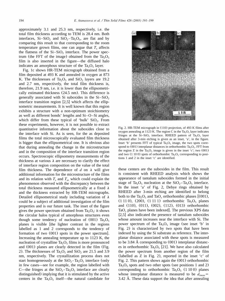
Fig. 2. HR-TEM micrograph in(110) projection, of 493 K films afteroxygen annealing at 1123 K. The region C in the Ta O layer indicates2 5
fringes at the Si–SiO interface. RHEED pattern of Ta O layer2 2 5
obtained after 3-min etching is given as an inset, ‘a’, in the figure.Inset ‘b’ presents FFT of typical Ta O image, the two spots corre-2 5
spond to(001) interplanar distances in orthorhombic Ta O . FFT from2 5
the region Z in the Ta O image is given in the inset ‘c’; two(001)2 5
and two(1 10 0) spots of orthorhombic Ta O corresponding to posi-2 5
tions 1 and 2 in the inset ‘c’ are identified.
approximately 3.1 and 25.3 nm, respectively, i.e. thetotal film thickness according to TEM is 28.4 nm. Bothinterfaces, Si–SiO and SiO –Ta O , are flat and by2 2 2 5
comparing this result to that corresponding to the roomtemperature grown films, one can argue thatT affectss
the flatness of the Si–SiO interface. The power spec-2
trum (the FFT of the image) obtained from the Ta O2 5
film is also inserted in the figure—the diffused haloindicates an amorphous structure of the Ta O layer.2 5
Fig. 1c shows HR-TEM micrograph obtained from afilm deposited at 493 K and annealed in oxygen at 873K. The thicknesses of Ta O and SiO layers are 19.22 5 2
and 2.7 nm, respectively, the total film thickness is,therefore, 21.9 nm, i.e. it is lower than the ellipsometri-cally estimated thickness(24.5 nm). This difference isgenerally associated with Si suboxides in the Si–SiO2
interface transition regionw2,5x which affects the ellip-sometric measurements. It is well known that this regionexhibits a structure with a non-optimum stoichiometryas well as different bonds’ lengths and Si–O–Siangles,which differ from these typical of ‘bulk’ SiO . From2
these experiments, however, it is not possible to extractquantitative information about the suboxides close tothe interface with Si. As is seen, for the as depositedfilms the total microscopically evaluated film thicknessis bigger than the ellipsometrical one. It is obvious alsothat during annealing the change in the microstructureand in the composition of the interface transition regionoccurs. Spectroscopic ellipsometry measurements of thethickness at variousl are necessary to clarify the effectof interface region composition on the value of the totalfilm thickness. The dependence ofd on l will giveadditional information for the microstructure of the filmsand its relation withT andT , which could explain thes a
phenomenon observed with the discrepancy between thetotal thickness measured ellipsometrically at a fixedland the thickness extracted by HR-TEM micrographs.Detailed ellipsometrical study including variation oflcould be a subject of additional investigation of the filmproperties and is our future task. The inset of the figuregives the power spectrum obtained from Ta O : it shows2 5
the circular halos typical of amorphous structures eventhough some tendency of nucleation of(001) Ta O2 5
planes is visiblewthe lighter contrast in the regionslabelled as 1 and 2 corresponds to the tendency offormation of two (001) spots in the power spectrumx.Increasing the annealing temperature up to 1123 K, thenucleation of crystalline Ta O films is more pronounced2 5
and (001) planes are clearly detected in the film(Fig.2). The thicknesses of Ta O and SiO are 21.5 and 3.92 5 2
nm, respectively. The crystallization process does notstart homogeneously at the SiO –Ta O interface(only2 2 5
in few cases—see for example, the region labelled withC—the fringes at the SiO –Ta O interface are clearly2 2 5
distinguished) implying that it is stimulated by the activecenters in the Ta O itself—the natural candidate for2 5
these centers are the suboxides in the film. This resultis consistent with RHEED analysis which shows theappearance of tantalum suboxides formed in the initialstage of Ta O nucleation at the SiO –Ta O interface.2 5 2 2 5
In the inset ‘a’ of Fig. 2, Debye rings obtained byRHEED after 3-min etching are identified to belongboth to the Ta O and TaO orthorhombic phasesw(001),2 5 x
(1 11 0), (200), (1 11 1) orthorhombic Ta O planes2 5
and (110), (011), (002), (112), (013) orthorhombicTaO planes have been indexedx. The previous XPS datax
w2,5x also indicated the presence of tantalum suboxideswhose amount increases near the interface with Si. Thepower spectrum of the Ta O image(see inset ‘b’ in2 5
Fig. 2) is characterized by two spots that have beenindexed by using the Si substrate as reference. The inter-planar distance associated with these spots is measuredto be 3.84 A corresponding to(001) interplanar distanc-˚es in orthorhombic Ta Ow21x. We have also calculated2 5
the power spectrum from another region of the film(labelled as Z in Fig. 2), reported in the inset ‘c’ ofFig. 2. This pattern shows again the(001) orthorhombicTa O spots and two other spots(see positions 1 and 2)2 5
corresponding to orthorhombic Ta O(1 10 0) planes2 5
whose interplanar distance is measured to bed smeas
3.42 A. These data support the idea that after annealing˚
195E. Atanassova et al. / Thin Solid Films 426 (2003) 191–199
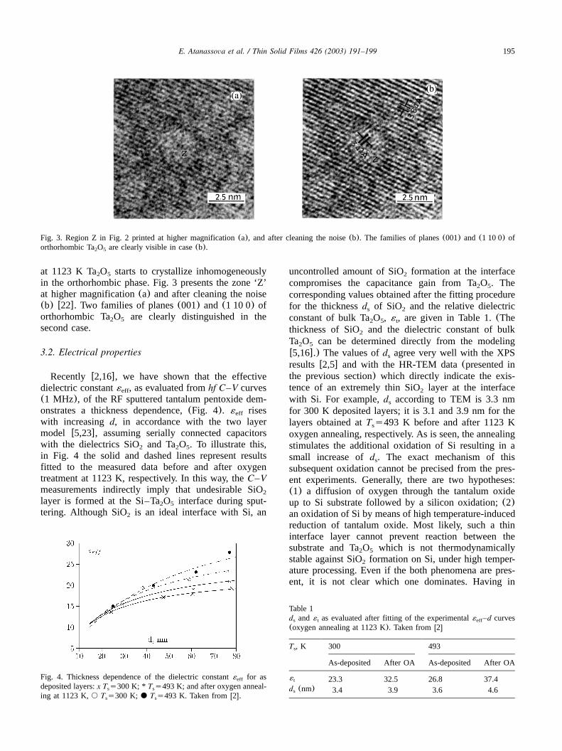
Fig. 3. Region Z in Fig. 2 printed at higher magnification(a), and after cleaning the noise(b). The families of planes(001) and (1 10 0) oforthorhombic Ta O are clearly visible in case(b).2 5
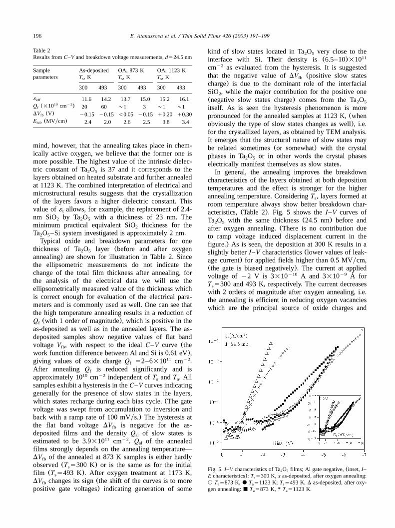
Fig. 4. Thickness dependence of the dielectric constant´ for aseff
deposited layers:x T s300 K; * T s493 K; and after oxygen anneal-s s
ing at 1123 K,s T s300 K; d T s493 K. Taken fromw2x.s s
Table 1d and´ as evaluated after fitting of the experimental´ –d curvess t eff
(oxygen annealing at 1123 K). Taken fromw2x
T , Ks 300 493
As-deposited After OA As-deposited After OA
´t 23.3 32.5 26.8 37.4d (nm)s 3.4 3.9 3.6 4.6
at 1123 K Ta O starts to crystallize inhomogeneously2 5
in the orthorhombic phase. Fig. 3 presents the zone ‘Z’at higher magnification(a) and after cleaning the noise(b) w22x. Two families of planes(001) and (1 10 0) oforthorhombic Ta O are clearly distinguished in the2 5
second case.
3.2. Electrical properties
Recently w2,16x, we have shown that the effectivedielectric constant́ , as evaluated fromhf C–V curveseff
(1 MHz), of the RF sputtered tantalum pentoxide dem-onstrates a thickness dependence,(Fig. 4). ´ riseseff
with increasingd, in accordance with the two layermodel w5,23x, assuming serially connected capacitorswith the dielectrics SiO and Ta O . To illustrate this,2 2 5
in Fig. 4 the solid and dashed lines represent resultsfitted to the measured data before and after oxygentreatment at 1123 K, respectively. In this way, theC–Vmeasurements indirectly imply that undesirable SiO2
layer is formed at the Si–Ta O interface during sput-2 5
tering. Although SiO is an ideal interface with Si, an2
uncontrolled amount of SiO formation at the interface2
compromises the capacitance gain from Ta O . The2 5
corresponding values obtained after the fitting procedurefor the thicknessd of SiO and the relative dielectrics 2
constant of bulk Ta O ,́ , are given in Table 1.(The2 5 t
thickness of SiO and the dielectric constant of bulk2
Ta O can be determined directly from the modeling2 5
w5,16x.) The values ofd agree very well with the XPSs
resultsw2,5x and with the HR-TEM data(presented inthe previous section) which directly indicate the exis-tence of an extremely thin SiO layer at the interface2
with Si. For example,d according to TEM is 3.3 nms
for 300 K deposited layers; it is 3.1 and 3.9 nm for thelayers obtained atT s493 K before and after 1123 Ks
oxygen annealing, respectively. As is seen, the annealingstimulates the additional oxidation of Si resulting in asmall increase ofd . The exact mechanism of thiss
subsequent oxidation cannot be precised from the pres-ent experiments. Generally, there are two hypotheses:(1) a diffusion of oxygen through the tantalum oxideup to Si substrate followed by a silicon oxidation;(2)an oxidation of Si by means of high temperature-inducedreduction of tantalum oxide. Most likely, such a thininterface layer cannot prevent reaction between thesubstrate and Ta O which is not thermodynamically2 5
stable against SiO formation on Si, under high temper-2
ature processing. Even if the both phenomena are pres-ent, it is not clear which one dominates. Having in
196 E. Atanassova et al. / Thin Solid Films 426 (2003) 191–199
Table 2Results fromC–V and breakdown voltage measurements,ds24.5 nm
Sample As-deposited OA, 873 K OA, 1123 Kparameters T , Ks T , Ks T , Ks
300 493 300 493 300 493
´eff 11.6 14.2 13.7 15.0 15.2 16.1Q (=10 cm )10 y2
f 20 60 ;1 3 ;1 ;1DV (V)fb y0.15 y0.15 -0.05 y0.15 q0.20 q0.30E , (MV ycm)bd 2.4 2.0 2.6 2.5 3.8 3.4
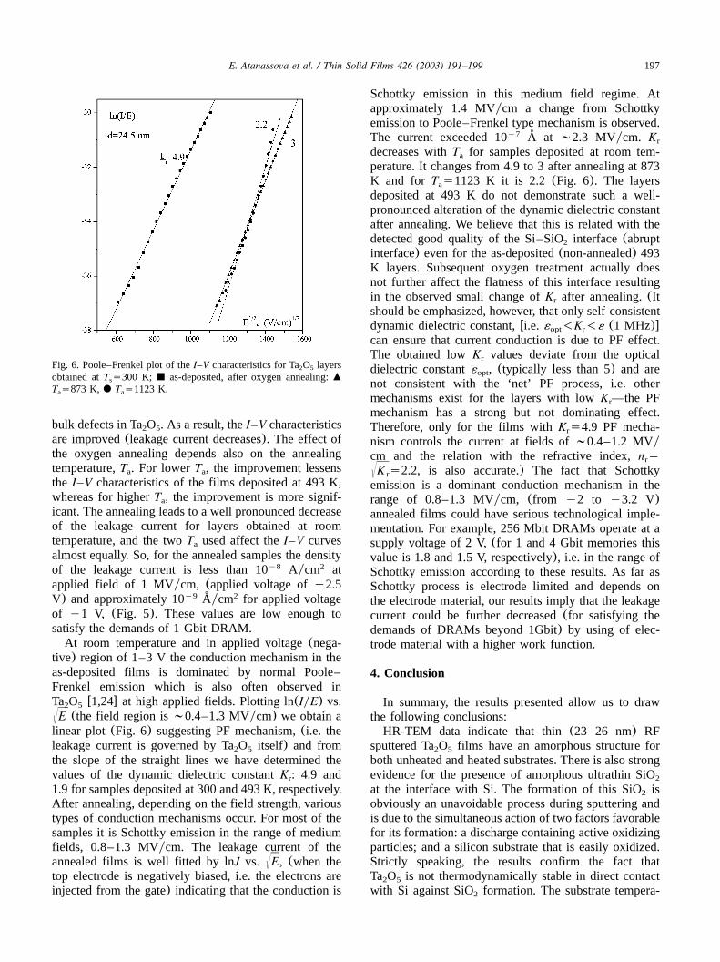
Fig. 5. I–V characteristics of Ta O films; Al gate negative,(inset,I–2 5
E characteristics): T s300 K, x as-deposited, after oxygen annealing:s
s T s873 K,d T s1123 K; T s493 K, D as-deposited, after oxy-a a s
gen annealing:j T s873 K, * T s1123 K.a a
mind, however, that the annealing takes place in chem-ically active oxygen, we believe that the former one ismore possible. The highest value of the intrinsic dielec-tric constant of Ta O is 37 and it corresponds to the2 5
layers obtained on heated substrate and further annealedat 1123 K. The combined interpretation of electrical andmicrostructural results suggests that the crystallizationof the layers favors a higher dielectric constant. Thisvalue of´ allows, for example, the replacement of 2.4-t
nm SiO by Ta O with a thickness of 23 nm. The2 2 5
minimum practical equivalent SiO thickness for the2
Ta O –Si system investigated is approximately 2 nm.2 5
Typical oxide and breakdown parameters for onethickness of Ta O layer(before and after oxygen2 5
annealing) are shown for illustration in Table 2. Sincethe ellipsometric measurements do not indicate thechange of the total film thickness after annealing, forthe analysis of the electrical data we will use theellipsometrically measured value of the thickness whichis correct enough for evaluation of the electrical para-meters and is commonly used as well. One can see thatthe high temperature annealing results in a reduction ofQ (with 1 order of magnitude), which is positive in thef
as-deposited as well as in the annealed layers. The as-deposited samples show negative values of flat bandvoltage V , with respect to the idealC–V curve (thefb
work function difference between Al and Si is 0.61 eV),giving values of oxide chargeQ s2–6=10 cm .11 y2
f
After annealing Q is reduced significantly and isf
approximately 10 cm independent ofT andT . All10 y2s a
samples exhibit a hysteresis in theC–V curves indicatinggenerally for the presence of slow states in the layers,which states recharge during each bias cycle.(The gatevoltage was swept from accumulation to inversion andback with a ramp rate of 100 mVys.) The hysteresis atthe flat band voltageDV is negative for the as-fb
deposited films and the densityQ of slow states issl
estimated to be 3.9=10 cm . Q of the annealed11 y2sl
films strongly depends on the annealing temperature—DV of the annealed at 873 K samples is either hardlyfb
observed(T s300 K) or is the same as for the initials
film (T s493 K). After oxygen treatment at 1173 K,s
DV changes its sign(the shift of the curves is to morefb
positive gate voltages) indicating generation of some
kind of slow states located in Ta O very close to the2 5
interface with Si. Their density is(6.5–10)=1011
cm as evaluated from the hysteresis. It is suggestedy2
that the negative value ofDV (positive slow statesfb
charge) is due to the dominant role of the interfacialSiO , while the major contribution for the positive one2
(negative slow states charge) comes from the Ta O2 5
itself. As is seen the hysteresis phenomenon is morepronounced for the annealed samples at 1123 K,(whenobviously the type of slow states changes as well), i.e.for the crystallized layers, as obtained by TEM analysis.It emerges that the structural nature of slow states maybe related sometimes(or somewhat) with the crystalphases in Ta O or in other words the crystal phases2 5
electrically manifest themselves as slow states.In general, the annealing improves the breakdown
characteristics of the layers obtained at both depositiontemperatures and the effect is stronger for the higherannealing temperature. ConsideringT , layers formed ats
room temperature always show better breakdown char-acteristics,(Table 2). Fig. 5 shows theI–V curves ofTa O with the same thickness(24.5 nm) before and2 5
after oxygen annealing.(There is no contribution dueto ramp voltage induced displacement current in thefigure.) As is seen, the deposition at 300 K results in aslightly betterI–V characteristics(lower values of leak-age current) for applied fields higher than 0.5 MVycm,(the gate is biased negatively). The current at appliedvoltage of y2 V is 3=10 A and 3=10 A fory10 y9 ˚T s300 and 493 K, respectively. The current decreasess
with 2 orders of magnitude after oxygen annealing, i.e.the annealing is efficient in reducing oxygen vacancieswhich are the principal source of oxide charges and
197E. Atanassova et al. / Thin Solid Films 426 (2003) 191–199
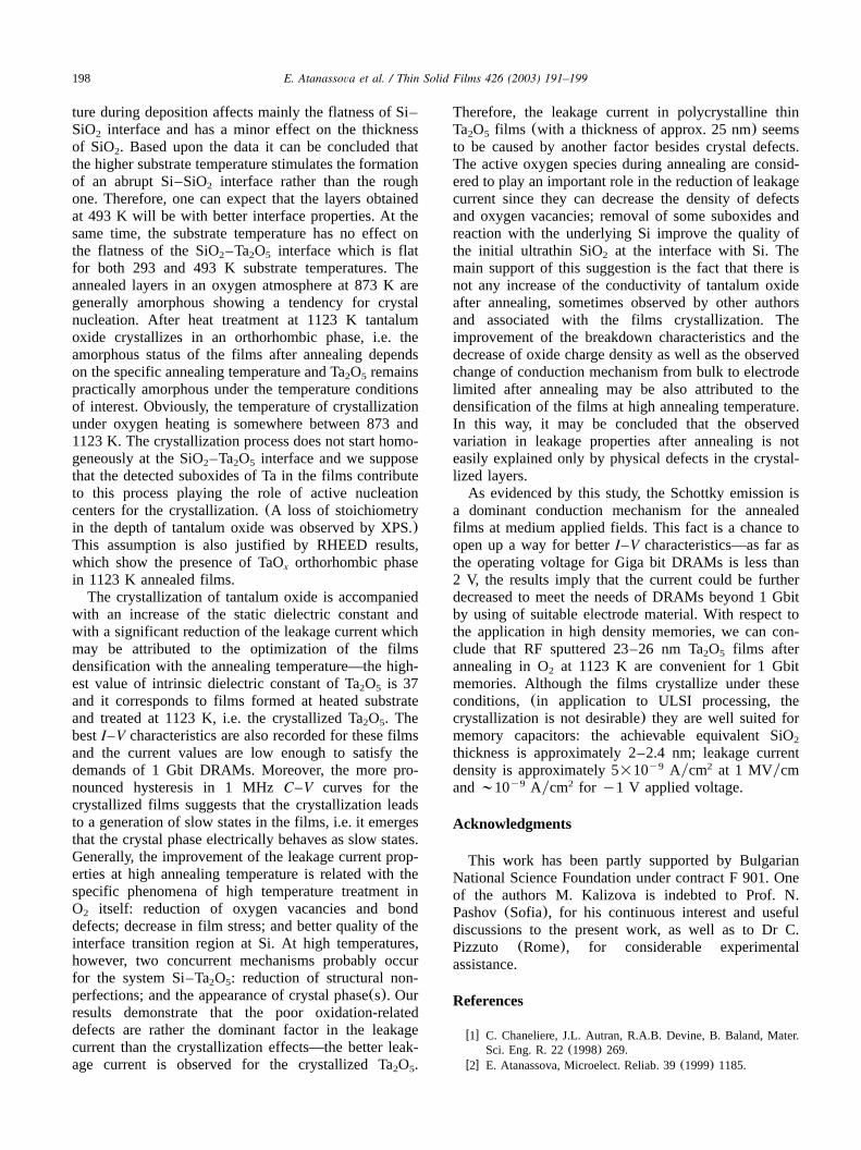
Fig. 6. Poole–Frenkel plot of theI–V characteristics for Ta O layers2 5
obtained atT s300 K; j as-deposited, after oxygen annealing:ms
T s873 K, d T s1123 K.a a
bulk defects in Ta O . As a result, theI–V characteristics2 5
are improved(leakage current decreases). The effect ofthe oxygen annealing depends also on the annealingtemperature,T . For lowerT , the improvement lessensa a
the I–V characteristics of the films deposited at 493 K,whereas for higherT , the improvement is more signif-a
icant. The annealing leads to a well pronounced decreaseof the leakage current for layers obtained at roomtemperature, and the twoT used affect theI–V curvesa
almost equally. So, for the annealed samples the densityof the leakage current is less than 10 Aycm aty8 2
applied field of 1 MVycm, (applied voltage ofy2.5V) and approximately 10 Aycm for applied voltagey9 2˚of y1 V, (Fig. 5). These values are low enough tosatisfy the demands of 1 Gbit DRAM.
At room temperature and in applied voltage(nega-tive) region of 1–3 V the conduction mechanism in theas-deposited films is dominated by normal Poole–Frenkel emission which is also often observed inTa O w1,24x at high applied fields. Plotting ln(IyE) vs.2 5
(the field region is;0.4–1.3 MVycm) we obtain ayElinear plot (Fig. 6) suggesting PF mechanism,(i.e. theleakage current is governed by Ta O itself) and from2 5
the slope of the straight lines we have determined thevalues of the dynamic dielectric constantK : 4.9 andr
1.9 for samples deposited at 300 and 493 K, respectively.After annealing, depending on the field strength, varioustypes of conduction mechanisms occur. For most of thesamples it is Schottky emission in the range of mediumfields, 0.8–1.3 MVycm. The leakage current of theannealed films is well fitted by lnJ vs. , (when theyEtop electrode is negatively biased, i.e. the electrons areinjected from the gate) indicating that the conduction is
Schottky emission in this medium field regime. Atapproximately 1.4 MVycm a change from Schottkyemission to Poole–Frenkel type mechanism is observed.The current exceeded 10 A at;2.3 MVycm. Ky7
r˚
decreases withT for samples deposited at room tem-a
perature. It changes from 4.9 to 3 after annealing at 873K and for T s1123 K it is 2.2 (Fig. 6). The layersa
deposited at 493 K do not demonstrate such a well-pronounced alteration of the dynamic dielectric constantafter annealing. We believe that this is related with thedetected good quality of the Si–SiO interface(abrupt2
interface) even for the as-deposited(non-annealed) 493K layers. Subsequent oxygen treatment actually doesnot further affect the flatness of this interface resultingin the observed small change ofK after annealing.(Itr
should be emphasized, however, that only self-consistentdynamic dielectric constant,wi.e. ´ -K -´ (1 MHz)xopt r
can ensure that current conduction is due to PF effect.The obtained lowK values deviate from the opticalr
dielectric constant́ , (typically less than 5) and areopt
not consistent with the ‘net’ PF process, i.e. othermechanisms exist for the layers with lowK —the PFr
mechanism has a strong but not dominating effect.Therefore, only for the films withK s4.9 PF mecha-r
nism controls the current at fields of;0.4–1.2 MVycm and the relation with the refractive index,n sr
, is also accurate.) The fact that SchottkyyK s2.2r
emission is a dominant conduction mechanism in therange of 0.8–1.3 MVycm, (from y2 to y3.2 V)annealed films could have serious technological imple-mentation. For example, 256 Mbit DRAMs operate at asupply voltage of 2 V,(for 1 and 4 Gbit memories thisvalue is 1.8 and 1.5 V, respectively), i.e. in the range ofSchottky emission according to these results. As far asSchottky process is electrode limited and depends onthe electrode material, our results imply that the leakagecurrent could be further decreased(for satisfying thedemands of DRAMs beyond 1Gbit) by using of elec-trode material with a higher work function.
4. Conclusion
In summary, the results presented allow us to drawthe following conclusions:
HR-TEM data indicate that thin(23–26 nm) RFsputtered Ta O films have an amorphous structure for2 5
both unheated and heated substrates. There is also strongevidence for the presence of amorphous ultrathin SiO2
at the interface with Si. The formation of this SiO is2
obviously an unavoidable process during sputtering andis due to the simultaneous action of two factors favorablefor its formation: a discharge containing active oxidizingparticles; and a silicon substrate that is easily oxidized.Strictly speaking, the results confirm the fact thatTa O is not thermodynamically stable in direct contact2 5
with Si against SiO formation. The substrate tempera-2
198 E. Atanassova et al. / Thin Solid Films 426 (2003) 191–199
ture during deposition affects mainly the flatness of Si–SiO interface and has a minor effect on the thickness2
of SiO . Based upon the data it can be concluded that2
the higher substrate temperature stimulates the formationof an abrupt Si–SiO interface rather than the rough2
one. Therefore, one can expect that the layers obtainedat 493 K will be with better interface properties. At thesame time, the substrate temperature has no effect onthe flatness of the SiO –Ta O interface which is flat2 2 5
for both 293 and 493 K substrate temperatures. Theannealed layers in an oxygen atmosphere at 873 K aregenerally amorphous showing a tendency for crystalnucleation. After heat treatment at 1123 K tantalumoxide crystallizes in an orthorhombic phase, i.e. theamorphous status of the films after annealing dependson the specific annealing temperature and Ta O remains2 5
practically amorphous under the temperature conditionsof interest. Obviously, the temperature of crystallizationunder oxygen heating is somewhere between 873 and1123 K. The crystallization process does not start homo-geneously at the SiO –Ta O interface and we suppose2 2 5
that the detected suboxides of Ta in the films contributeto this process playing the role of active nucleationcenters for the crystallization.(A loss of stoichiometryin the depth of tantalum oxide was observed by XPS.)This assumption is also justified by RHEED results,which show the presence of TaO orthorhombic phasex
in 1123 K annealed films.The crystallization of tantalum oxide is accompanied
with an increase of the static dielectric constant andwith a significant reduction of the leakage current whichmay be attributed to the optimization of the filmsdensification with the annealing temperature—the high-est value of intrinsic dielectric constant of Ta O is 372 5
and it corresponds to films formed at heated substrateand treated at 1123 K, i.e. the crystallized Ta O . The2 5
bestI–V characteristics are also recorded for these filmsand the current values are low enough to satisfy thedemands of 1 Gbit DRAMs. Moreover, the more pro-nounced hysteresis in 1 MHzC–V curves for thecrystallized films suggests that the crystallization leadsto a generation of slow states in the films, i.e. it emergesthat the crystal phase electrically behaves as slow states.Generally, the improvement of the leakage current prop-erties at high annealing temperature is related with thespecific phenomena of high temperature treatment inO itself: reduction of oxygen vacancies and bond2
defects; decrease in film stress; and better quality of theinterface transition region at Si. At high temperatures,however, two concurrent mechanisms probably occurfor the system Si–Ta O : reduction of structural non-2 5
perfections; and the appearance of crystal phase(s). Ourresults demonstrate that the poor oxidation-relateddefects are rather the dominant factor in the leakagecurrent than the crystallization effects—the better leak-age current is observed for the crystallized Ta O .2 5
Therefore, the leakage current in polycrystalline thinTa O films (with a thickness of approx. 25 nm) seems2 5
to be caused by another factor besides crystal defects.The active oxygen species during annealing are consid-ered to play an important role in the reduction of leakagecurrent since they can decrease the density of defectsand oxygen vacancies; removal of some suboxides andreaction with the underlying Si improve the quality ofthe initial ultrathin SiO at the interface with Si. The2
main support of this suggestion is the fact that there isnot any increase of the conductivity of tantalum oxideafter annealing, sometimes observed by other authorsand associated with the films crystallization. Theimprovement of the breakdown characteristics and thedecrease of oxide charge density as well as the observedchange of conduction mechanism from bulk to electrodelimited after annealing may be also attributed to thedensification of the films at high annealing temperature.In this way, it may be concluded that the observedvariation in leakage properties after annealing is noteasily explained only by physical defects in the crystal-lized layers.
As evidenced by this study, the Schottky emission isa dominant conduction mechanism for the annealedfilms at medium applied fields. This fact is a chance toopen up a way for betterI–V characteristics—as far asthe operating voltage for Giga bit DRAMs is less than2 V, the results imply that the current could be furtherdecreased to meet the needs of DRAMs beyond 1 Gbitby using of suitable electrode material. With respect tothe application in high density memories, we can con-clude that RF sputtered 23–26 nm Ta O films after2 5
annealing in O at 1123 K are convenient for 1 Gbit2
memories. Although the films crystallize under theseconditions, (in application to ULSI processing, thecrystallization is not desirable) they are well suited formemory capacitors: the achievable equivalent SiO2
thickness is approximately 2–2.4 nm; leakage currentdensity is approximately 5=10 Aycm at 1 MVycmy9 2
and;10 Aycm for y1 V applied voltage.y9 2
Acknowledgments
This work has been partly supported by BulgarianNational Science Foundation under contract F 901. Oneof the authors M. Kalizova is indebted to Prof. N.Pashov(Sofia), for his continuous interest and usefuldiscussions to the present work, as well as to Dr C.Pizzuto (Rome), for considerable experimentalassistance.
References
w1x C. Chaneliere, J.L. Autran, R.A.B. Devine, B. Baland, Mater.Sci. Eng. R. 22(1998) 269.
w2x E. Atanassova, Microelect. Reliab. 39(1999) 1185.
199E. Atanassova et al. / Thin Solid Films 426 (2003) 191–199
w3x A.I. Kingon, J.P. Maria, S.K. Streiffer, Nature 406(2000)1032.
w4x G.D. Wilk, R.M. Wallace, J.M. Antony, J. Appl. Phys. 89(2001) 5243.
w5x E. Atanassova, T. Dimitrova, in: H.S. Nalwa(Ed.), Handbookof Surfaces and Interfaces of Materials, 4, Academic Press,San Diego, USA, 2001, p. 439.
w6x G.S. Oehrlein, F.M. d’Heurle, A. Reisman, J. Appl. Phys. 55(1984) 3715.
w7x C. Hashimoto, H. Oikawa, in: Extended abstracts, 17th Con-ference on Solid State Devices and Materials, Tokyo, 1985, p.275.
w8x S. Roberts, J. Ryan, L. Nesbit, J. Electrochem. Soc. 133(1986)1405.
w9x S.R. Jeon, S.W. Han, J.W. Park, J. Appl. Phys. 77(1995)5978.
w10x E.P. Burte, N. Rausch, J. Non-Cryst. Solids 187(1995) 425.w11x C. Isole, M. Saitoh, Appl. Phys. Lett. 56(1990) 907.w12x S. Tanimoto, M. Matsui, K. Kamisako, K. Kuroiwa, Y. Tarnis,
J. Electrochem. Soc. 139(1992) 320.w13x K. Shimizu, M. Katajama, H. Funaki, E. Arai, M. Nakata, Y.
Ohji, R. Imura, J. Appl. Phys. 74(1993) 375.w14x S. Kamiyama, H. Suzuki, H. Watanabe, A. Sakai, H. Kimura,
J. Mitzuki, J. Electrochem. Soc. 141(1994) 1246.w15x Y. Matsui, K. Torii, M. Hirayama, Y. Fujisaki, S. Iijima, Y.
Ohji, IEEE Electron. Dev. Lett. 17(1996) 431.
w16x T. Dimitrova, E. Atanassova, Solid State Electron. 42(1998)307.
w17x M. Kalitzova, A. Peeva, E. Atanassova, G. Vitali, G. Zollo, C.Pizzuto, Materials for information technology and new millen-nium, in: J.M. Marshall, A.G. Petrov, A. Vavrek, D. Nesheva,D. Dimova-Malinovska, J.M. Maud(Eds.) Proceedings of the11th International School on Condensed Matter Physics, Sep-tember 2000, Varna, Bulgaria, World Science Singapore, 2001,p. 252.
w18x T. Dimitrova, K. Arshak, E. Atanassova, Materials for infor-mation technology and new millennium, in: J.M. Marshall,A.G. Petrov, A. Vavrek, D. Nesheva, D. Dimova-Malinovska,J.M. Maud(Eds.). Proceedings of the 11th International Schoolon Condensed Matters Physics, September 2000, Varna, Bul-garia, World Science Singapore, 2001, p. 244.
w19x A. Romano, J. Vanhellemont, H. Bender, J.R. Morante, Ultra-microscopy 31(1989) 183.
w20x A.F. De Jong, W. Coene, D. Van Dyck, Ultramicroscopy 27(1989) 53.
w21x X-Ray diffraction file, ASTM.w22x D. Van Dyck, Ultramicroscopy 55(1994) 99.w23x Y. Nishioka, S. Kimura, H. Shinriki, K. Mukai, J. Electrochem.
Soc. 134(1987) 410.w24x S. Barnejee, B. Shen, I. Chen, J. Bohlman, G. Brown, R.
Doering, J. Appl. Phys. 65(1989) 1140.
Copyright © 2022 FDOKUMEN