On the electrostatic potential profile in biased molecular wires
Upload
independentCategory
view
8download
0
52 IEEE JOURNAL OF SOLID-STATE CIRCUITS, VOL. 43, NO. 1, JANUARY 2008
High Speed and Low Energy CapacitivelyDriven On-Chip Wires
Ron Ho, Member, IEEE, Tarik Ono, Robert David Hopkins, Member, IEEE, Alex Chow, Member, IEEE,Justin Schauer, Frankie Y. Liu, Member, IEEE, and Robert Drost, Member, IEEE
Abstract—We present circuits for driving long on-chip wiresthrough a series capacitor. The capacitor improves delay throughsignal pre-emphasis, offers a reduced voltage swing on the wire forlow energy without a second power supply, and reduces the drivenload, allowing for smaller drivers. Sidewall wire parasitics usedas the series capacitor improve process tracking, and twisted andinterleaved differential wires reduce both coupled noise as wellas Miller-doubled cross-capacitance. Multiple drivers sharing atarget wire allow simple FIR filters for driver-side pre-equaliza-tion. Receivers require DC bias circuits or DC-balanced data. Atestchip in a 180 nm, 1.8 V process compared capacitively-cou-pled long wires with optimally-repeated full-swing wires. At a200 mV swing, we measured energy savings of 3.8X over full-swingwires. At a 50 mV swing, we measured energy savings of 10.5X.Throughput on a 14 mm wire experiment due to capacitor pre-em-phasis improved 1.7X using a 200 mV swing.
Index Terms—Capacitance, electromagnetic coupling, inte-grated circuit interconnections, very large scale integration.
I. LATENCY AND ENERGY PROBLEMS OF ON-CHIP WIRES
AS VLSI technologies continue to scale, on-chip wires willpresent increasing latency and energy problems. Their
shrinking cross-sectional area and hence increased electricalresistance means that cross-chip repeated wire delays will farexceed transistor delays [1]. To prevent this from throttlingsystem performance, designers are building modular systemswith multiple on-die cores (e.g., [2], [3]). These machines allowfast local communication to dictate thread performance whilescheduling slower cross-chip data transfers over a dedicatedon-chip network. However, the high latency of cross-chipcommunication can still limit total performance: it increasesthe delay to on-die caches, it slows down snooping-based cachecoherence, and it increases the size of buffers used to holdoutstanding global requests.
Due to their switched capacitances, on-chip wires alsopresent an increasing energy problem. A CMOS wire driverrunning at an effective frequency must switch a total wirecapacitance through the voltage , leading to a powercost proportional to . Under technology scaling,remains largely constant (for global wires spanning con-stant-sized die), scales down only slowly, and scales up,leading to nearly constant power per wire. However, with chips
Manuscript received April 16, 2007; revised August 8, 2007. This work wassupported in part by the Defense Advanced Research Projects Agency (DARPA)under Contract NBCH30390002.
The authors are with Sun Microsystems Research Labs, Menlo Park, CA94025 USA (e-mail: [email protected]).
Digital Object Identifier 10.1109/JSSC.2007.910807
becoming increasingly integrated and containing more andmore devices, this constant power per wire gets multiplied byan ever-increasing number of wires. For instance, each chip in adata-routing grid for a high-productivity computer system maycarry in excess of 250 meters of global wiring, which wouldburn nearly 50 W of wire and repeater power at 4 GHz, a 10%activity factor, and a 1 V supply [4].
There are many interesting solutions to the problemsof on-chip wires. On-chip transmission lines offer nearspeed-of-light latency and an appealingly high throughput[5]–[7]. However, because they need to be wide enough toprevent wire resistance from swamping out wire inductance,they typically offer less throughput per cross-sectional area thana set of densely packed repeated wires. For example, in one180 nm design, 8 Gb/s coplanar transmission lines consume32 m per bit [6], for a throughput density of 0.25 Gb/s m. Inanother design, 14 Gb/s microstrip transmission lines consumejust under 20 m per bit, but require signals on M6 running overa M2 ground to model a thick dielectric, thus using significantlymore wire resources [7]; depending on how one counts thecost of the open M3–M5, this is at most a throughput densityof 0.35 Gb/s m. By contrast, wide global wires in a 180 nmtechnology can use 1.6 m per bit and run at 1 Gb/s, for a muchbetter throughput density of 0.625 Gb/s m, and with simplerclocking.
Other solutions use CMOS repeaters but improve their per-formance through channel equalization techniques. One methodimplements an unrolled decision-feedback equalization (DFE)scheme, in which each bit is evaluated by a comparator witha scaled version of the previous bit used as an offset [8]. Byreducing the number of repeaters required, this DFE schemecan reduce average power by up to 35%. Another equaliza-tion technique periodically boosts the line using circuits thatsense transitions and then “kick” in additional current to im-prove rise/fall times [9]. As with earlier versions of this tech-nique [10], improved performance of around 20% comes withreduced noise margins. Circuits using optimized low-voltageswings have shown a 10X energy savings, but at a 30% latencypenalty and reduced noise margins [11]. More problematically,such low-swing systems typically require an expensive secondpower supply, which breaks up power distribution planes on thechip and in the package and necessitates additional voltage reg-ulator modules at low target impedances.
We discuss new circuits for long on-chip wires that reduceboth latency and energy when compared to conventionally re-peated wires. We use reduced voltage swings to enable signifi-cant energy savings, albeit with reduced noise margins, and weuse pre-emphasis to enable higher performance, with a moderateincrease in layout complexity.
0018-9200/$25.00 © 2008 IEEE

HO et al.: HIGH SPEED AND LOW ENERGY CAPACITIVELY DRIVEN ON-CHIP WIRES 53
Fig. 1. Driving a wire with a capacitor reduces voltage swing and providespre-emphasis.
A coupling capacitor in-line with the long wire pre-empha-sizes transitions to reduce wire delay and to reduce the loadseen by the driver [12], [13]. It also lowers the wire’s voltageswing without a second power supply. Analysis shows that anunrepeated capacitively driven 10 mm wire is slightly fasterand much lower power than a conventionally repeated 10 mmglobal wire. Measured results at a 10 mm wire length in 180 nmCMOS show 10.5X energy savings at a 50 mV swing comparedto full-swing repeated wires. A second comparison, designedto show higher wire performance, compared full-swing 14 mmunrepeated wires to capacitively-driven wires using a 200 mVsignal swing; these measurements showed a 1.7X improvementin throughput.
II. CAPACITIVELY-COUPLED WIRES
Driving a long wire of capacitance through a capacitorreduces the signal swing on the wire through a capacitive
voltage divider. As shown in Fig. 1, including parasitic capac-itance on the right side of the coupling capacitor and in-cluding the final load capacitance gives a final wire voltageswing of . Typically,
and are both small compared to , so a wire swingof 50 mV in a 1.8 V technology thus uses a coupling capacitor
.The node immediately after the coupling capacitance will ini-
tially overshoot and then settle to , while the end of thewire will show a rapid rise to the final voltage. The sim-ulation waveforms embedded in the figure illustrate this risingedge at both ends of the wire, for both a simple single- modelas well as for a distributed wire model discussed below. Drivingthe long wire through the series coupling capacitor offers twoprincipal benefits.
A. Bandwidth Extension Through Pre-Emphasis
Because it acts as a high-frequency short, the capacitor in-creases the 3-dB bandwidth of the long wire, allowing shortercycle times and decreasing latency. Long wires have a low-pass
Fig. 2. Simulations of bandwidth improvement on a 14 mm minimum-widthunrepeated wire.
Fig. 3. Bandwidth improvement with capacitor ratio.
frequency response that limits their operating speed. Capacitivecoupling to a long wire creates a pole-zero pair, giving high-fre-quency emphasis that mitigates the low-pass wire response andincreases performance.
Fig. 2 shows the simulated frequency response of a min-imum-width 14 mm long on-chip wire, and how its 3-dBbandwidth improves 3.4X with the addition of capacitivecoupling. This is simply an illustration of the well-knowntradeoff between voltage gain and signal bandwidth, as thehigher-bandwidth curve reflects 1/20th the voltage amplitude.An important consequence of the bandwidth extension is thereduction in the number of repeater stages along the wire,saving area, energy, and routing complexity. Fig. 3 showshow the bandwidth improvement of the long wire varies withcoupling capacitance.
In practice, however, the resulting throughput improvementis typically about half this bandwidth gain. This is because re-duced swing wires require differential signaling, which con-sumes double the wire resources. So a better measurement ofthe throughput improvement—one that holds total wire pitchconstant—ought to compare the capacitively-coupled wire to afull-swing wire of double the wire resources.
The latency improvement of the capacitively-driven wire canbe seen in the step response at the end of the long wire. Usinga -model for the wire, as shown in Fig. 1, leads to a single-

54 IEEE JOURNAL OF SOLID-STATE CIRCUITS, VOL. 43, NO. 1, JANUARY 2008
Fig. 4. A differential link.
pole approximation with a time constant shown below. In thisestimate, we assume and .
This is faster than an inverter driving a wire because the driversees only , not , and because charge redistribution acrossthe wire effectively cuts the wire delay in half. Of course, thissimple model is pessimistic because it limits the pre-emphasisspike immediately after the capacitor to . A distributedwire model more accurately shows a larger pre-emphasis spikeimmediately after the capacitor, which in turn charges the wirefaster. However, the simple model offers quick delay estimatesand intuition for the circuit’s latency benefit.
B. Reduced Energy
The capacitor reduces the energy required to switch the longwire both by reducing the voltage swing, and also by reducingthe effective wire load seen by the driver.
In reducing the voltage swing, the capacitor offers energy sav-ings linear to the reduced voltage swing, without requiring asecond power supply. Building a power supply in a high-perfor-mance microprocessor entails significant expense due to its lowtarget impedance. Target impedance, a ratio of allowed voltageripple to transient current, is falling 5X per generation and is atmicro- levels in modern processors [14]; maintaining this lowimpedance across many decades of frequency requires expen-sive capacitors and extensive design work. For a dedicated low-voltage power supply used to drive wires, the transient currentwill be lower, but so will the tolerated voltage ripple, leading toa target impedance only slightly better than the rest of the chip’ssupply. Recent explorations in switching linear power regulatorsmake dedicated secondary power supplies more palatable [15],but the simplicity of a driving capacitor remains appealing.
By reducing the effective wire load seen by the driver, the ca-pacitor allows the driver size to be dramatically reduced. Typicallow-swing wire circuits drive the full wire load of , requiringa proportionally-sized driver. In such systems, the large driverdominates the overall energy, limiting the available energy sav-ings. By contrast, a series capacitor reduces the driven capac-itance to , under 1/36th of the original wireload in the above 50 mV example. This in turn allows for muchsmaller drivers, saving area and energy. Of course, this savingsis reduced somewhat by a need for the coupling capacitor, dif-ferential wires (discussed below), and a differential sense-am-plifier; a single bit link is shown in Fig. 4.
Fig. 5. Coupling capacitor pitchfork.
III. CAPACITOR LAYOUT ISSUES
Ideally, the series coupling capacitor would be bias-indepen-dent and require no special processing steps. In addition, be-cause the voltage swing is set by the ratio of the coupling ca-pacitance to the wire capacitance, we preferred a capacitor thatwould track the wire capacitances under process variations. Forthese reasons, we ruled out using transistor capacitors or specialmetal-insulator-metal (MIM) layers.
In modern VLSI layout technologies, intrinsic sidewallcapacitance between neighboring wires dominates the totalwire capacitance. This is typically viewed as a disadvantage fornoise reasons; however, in this case it enables us to make cou-pling capacitors using a “pitchfork” structure. Fig. 5 is a screencapture of a metal pitchfork from Electric, an open-sourceJava-based CAD integrated design environment [16]. This ca-pacitance tracks wire process variations, keeping the couplingratio constant. Using multiple “tines” on the fork, orextending the pitchfork to multiple metal layers, will reducethe total length of the capacitor.
For a 150 mV swing in a 1.8 V system, a 1 cm wire mightrequire a 50 m-long pitchfork with nine driver tines interleavedwith ten wire tines. In practice, pitchfork lengths can be evenshorter because the downstream long wire may use a wire-to-wire spacing larger than in the pitchfork, although this gives upsome process variation tracking.
The long wire portion of the pitchfork contains the outer tines,while the driver portion of the pitchfork nestles inside. This ar-rangement puts parasitic capacitance to ground on the long wireside of the coupling capacitor, where the capacitive divider ef-fectively reduces its impact on the driver. If the tines were re-versed, the outer tine parasitics would be fully visible to thedriver and contribute more to the total energy and delay of thesystem.
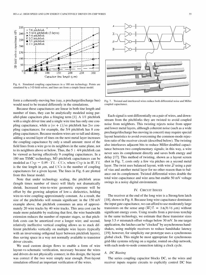
The points in Fig. 6 show 3-D field solver simulations forpitchfork capacitance models, using various configurations ofdriver and wire tines. In this plot, a “5/4 pitchfork” representsa structure with 5 wire-side tines and 4 driver-side tines. Thesesimulations mostly used pitchforks on the M3 layer in a 180 nmtechnology, with minimum-pitch orthogonal M4 and M2 wireseffectively acting as grounds. The exception is the 2-layer pitch-fork, labeled “5 4/4 pitchfork,” which used 5 tines on M3and four tines on M2 for the long wire and minimum pitch or-thogonal wires on M4 and M1 acting effectively as grounds. Inall cases, the orthogonal wires need not be actually grounded,but are treated as such in the simulations. Orthogonal wires that
HO et al.: HIGH SPEED AND LOW ENERGY CAPACITIVELY DRIVEN ON-CHIP WIRES 55
Fig. 6. Simulated coupling capacitances in a 180 nm technology. Points aresimulated by a 3-D field solver, and lines are from a simple linear model.
form a coherently-moving bus (say, a precharge/discharge bus)would need to be treated differently in the simulations.
Because these capacitances are linear in both tine length andnumber of tines, they can be analytically modeled using par-allel-plate capacitors plus a fringing term [1]. A 1/1 pitchforkwith a single driver tine and a single wire tine has only one cou-pling capacitance, while a pitchfork has cou-pling capacitances; for example, the 5/4 pitchfork has 8 cou-pling capacitances. Because modern wires are so tall and skinny,adding a second layer of tines on the next metal layer increasesthe coupling capacitance by only a small amount: most of thefield lines from a wire go to its neighbors in the same plane, notto its neighbors above or below. Thus, the 5 4/4 pitchfork canbe viewed as having effectively 9 coupling capacitances. In a180 nm TSMC technology, M3 pitchfork capacitances can bemodeled as , where is in fF,is the tine length in m, and is the number of couplingcapacitances for a given layout. The lines in Fig. 6 are plottedfrom this linear model.
Note that under technology scaling, the pitchfork areas(length times number of tines) will likely not dramaticallyshrink. Increased wire-to-wire geometric exposure will beoffset by the growing adoption of low- dielectrics, holdingwire-to-wire coupling approximately constant. As a result, thesize of the pitchforks will remain significant: in the 150 mVexample above, the pitchfork consumes an area of approxi-mately 20 wire tracks by 40 wire tracks. This area cost can bemade more palatable by realizing that first, the wire bandwidthextension reduces the number of repeater stages, so that pitch-fork costs can be amortized over a longer wire; and second,relatively ineffective vertical coupling allows us to stack dif-ferent pitchforks vertically on multiple wire layers (typicallywith an invervening orthgonal layer between pitckfork layers),thus saving space in a way not normally available to transistordriver circuits.
We used custom design flows to enable a form of wirelayout-vs-schematic verification, necessary because the wiresand drivers do not physically connect; in this design, the layoutwas correct if the two were simply near enough. Post-layoutsimulation offered an important verification of the wires.
Fig. 7. Twisted and interleaved wires reduce both differential noise and Millercoupled capacitance.
Each signal is sent differentially on a pair of wires, and down-stream from the pitchforks they are twisted to avoid couplednoise from neighbors. This twisting rejects noise from upperand lower metal layers, although coherent noise (such as a wideprecharge/discharge bus moving in concert) may require speciallayout heuristics to avoid overcoming the common-mode rejec-tion ratio of the receiver circuit (described below). The twistingalso interleaves adjacent bits to reduce Miller-doubled capaci-tance between two complementary signals; in this way, a wirenever sees its complement directly and saves both energy anddelay [17]. This method of twisting, shown as a layout screenshot in Fig. 7, costs only a few via pitches on a second metallayer. The twist uses balanced layout, with wire using a pairof vias and another metal layer for no other reason than to bal-ance out its complement. Twisted differential wires double thetotal wire capacitance and wire area but enable 50 mV voltageswings in a noisy digital environment.
IV. CIRCUIT ISSUES
The receiver at the end of the long wire is a StrongArm latch[18], shown in Fig. 8. Because long wire capacitance dominatesthe input gate capacitance, we can afford to use moderately largetransistors on the sense amp m withoutsignificant energy costs. Using results from a previous testchipin the same technology, we estimate that these transistor sizeskeep 3.5 mismatch offset voltage below 30 mV. In one targetapplication, the latches can be “clocked” by asynchronous hand-shakes, using multiple receivers to reduce handshake latency[19]; however, for simplicity our prototype uses a synchronousglobal clock. This might be most appropriate for synchronousgrid-like systems relying on a regular, routed on-chip network,with each node-to-node connection taking a clock cycle.
A. DC Biasing
The series coupling capacitor blocks DC, so the wires andreceiver inputs require circuits to explicitly control DC bias

56 IEEE JOURNAL OF SOLID-STATE CIRCUITS, VOL. 43, NO. 1, JANUARY 2008
Fig. 8. Regenerative differential receiver.
Fig. 9. Driver, sized to drive a 7 mm wire.
voltage. More precisely, the receiver inputs need to be initiallyset to the correct voltage, in order to operate, and then they needto be maintained at that voltage in spite of any transistor channelor gate leakage. This biasing can be done in several ways.
First, the wires can be precharged each cycle to , but sucha high switching activity would defeat any potential energy sav-ings from using small swings. Better yet, all of the wires couldbe precharged every few hundred microseconds: stop the trans-mitters and receivers, set both true and complement drivers to
(using a small shorting transistor, as shown in Fig. 9)and then refresh the wires to . Because this can be a rela-tively slow and rare event, the refresh transistors can be small.However, this periodic stopping exposes the physical link char-acteristics at the microarchitectural level, complicating systemdesigns.
Alternately, we could build channels for an -bit bus.At any time, one of the channels is precharging, whilethe other channels carry data. After the extra channel finishesprecharging, it replaces an operating channel, which then getsdisconnected and precharged. During channel replacement, thechannels will use a “make-before-break” method to ensure thatat no time does a bit lose its channel. By rotating the single re-freshing channel through the set, we can essentially hidethe refresh, for a small overhead in multiplexors. A simple im-plementation ties each data bit to two neighboring channels, sobit 0 is tied to channels 0 and 1, bit 1 is tied to channels 1 and2, and so on, with bit tied to channels and . Thisallows the refreshing channel to “walk” from 0 to andthen back down again, repeating as needed. This swapping ofan extra channel is directly analogous to how high-speed linksperform on-going receiver calibration. The energy overhead of
this rotation includes the switches on each of the channels, atboth driver and receiver ends. These switches can be relativelysmall and low capacitance. The overhead also includes the dy-namic refresh operation, which should be small if it happens ona microsecond time basis.
Our prototype uses a third bias scheme and leverages the factthat the target system uses optical links to carry data betweengroups of chips [4]. As a result, data traffic across the system,and hence across each chip, will be DC-balanced. In this case,we simply connect each receiver input to through a leaky(off) pMOS transistor whose time constant is hundreds of
(as shown on the inputs in Fig. 8). If the data is DC-balancedat that timescale, and thus has both a balanced number of “0”sand “1”s as well as a maximum number of consecutive identicalbits, the receiver inputs will not drift far from their bias point.
A similar but independent design, also using capacitive cou-pling, solves the DC bias problem with a receiver-side load re-sistance coupled with a driver-side transconductance[20]. The constraints are that the time constants and
should be approximately equal, that should be small,and that should be large. This both maintains the pre-em-phasis benefit of the capacitor as well as minimizes staticcurrent.
In all cases, we chose to bias the receivers at in orderto maximize the performance of the input nMOS transistors.This leads to a small over-voltage on the gates of these de-vices, by 25 mV to 100 mV in our experiments. This was notenough to cause reliability issues on the 180 nm or 90 nm tech-nologies explored in our studies; however, future technologyscaling to 45 nm and below may limit the amount of accept-able over-voltage, complicating the DC biasing.
B. Driver Circuits
The drivers, shown in Fig. 9, can be small inverters with ashorting transistor between input and output. This holds thedriver output at during powerup, while the receiver’sweak bias pulls the wire to . Because the shorting devicedoes not activate during normal operation, it can be quite small
m .Multiple pitchfork capacitors can also connect to a common
long wire, with the resulting signal on the wire the sum of thecapacitor displacement currents. We can use this to create pro-grammable varactors that allow post-fabrication adjustment ofthe effective coupling capacitance. For example, we designed adriver connected to three pitchfork capacitors, all tied togetheron the long wire side with pMOS transistor switches that operatearound a voltage bias. These switches increased the effec-tive wire-side load and added a series resistance; when sized formaximum throughput, they reduced the bandwidth by less than8%, but enabled selectable voltage swings of 50 mV, 150 mV,or 250 mV in a 1.8 V technology. Alternatively, the switchesfor the varactor can sit on the driver side of the pitchforks. Thisavoids any decrease in bandwidth, but requires complementarypassgates as well as a much larger driver or several drivers.
This ability to inexpensively create capacitive summing junc-tions eases the implementation of driver-side channel equaliza-tion techniques [21]. For example, we can create a two-tap FIRfilter by driving not only the current bit, but also an inverted and

HO et al.: HIGH SPEED AND LOW ENERGY CAPACITIVELY DRIVEN ON-CHIP WIRES 57
Fig. 10. Two-tap FIR filter built from capacitors.
Fig. 11. Bandwidth improvement and corresponding tap weight from a two-tapfilter, as a function of tap delay, for a 14 mm unrepeated minimum width wire.Solid curve shows bandwidth improvement. Dashed line shows the ideal weightof the second tap, for each possible tap delay.
scaled copy of the previous bit (see Fig. 10). Similar techniqueshave proven useful in off-chip communication, but are expen-sive to implement on a chip; however, series capacitors simplifythe FIR filter significantly. In the simple implementation shown,the second tap is delayed by a clock cycle, which may not beoptimal.
Fig. 11 explores a two-tap FIR filter for a 14 mm minimum-width unrepeated wire. The wire was originally designed to bedriven using a capacitor sized for a 200 mV swing, and then hada second tap added to the design. Fig. 11 shows, for each choiceof the second tap’s delay, the tap weight (and correspondingbandwidth improvement) that gives the smallest energy-delayproduct on the 14 mm wire. The additional driver energy costfor using the second tap is proportional to . Thefigure shows that short tap delays provide bandwidth improve-ment but at increased energy cost; the tap delay with the highestbandwidth/energy ratio is at 1 nS.
C. Energy-Delay Analysis
Fig. 12 shows simulations comparing repeaters to capaci-tively driven wires for a 10 mm link in a 180 nm process. Be-cause the figure plots energy on the Y-axis, and performance(the reciprocal of delay) on the X-axis, “better” circuits arecloser to the bottom right corner. Because any single designoccupies a single point on this graph, we can compare the en-ergy-delay product of any two circuit designs by contrasting theslope of the line connecting their points to the origin.
Fig. 12. Energy-delay analysis comparing capacitive drivers to conventionalrepeaters. Dashed lines indicate the improvment in both latency and power inthe simulations.
In general, as we sweep a design’s parameters, such asor sizing, circuits trace curves that bend up and to the right, re-flecting the growing incremental energy cost of faster and fasterperformance. Likewise, curves also tend to bend down and tothe left, illustrating that trying to find the absolute minimum en-ergy design has a high incremental performance cost. Withoutexternally imposed specifications for delay or energy, designersgenerally strive to put their circuits towards the knee of thesecurves, where the sensitivity of both energy and performance toa design parameter is balanced.
To generate the traces for the repeaters, our simulations variedrepeater size, with spacing set by the number of repeaters. Forone repeater, a driver and a repeater broke the line into two 5 mmsegments; for two repeaters, three stages drove 3.33 mm each;and for three repeaters, the driver and three stages each drove2.5 mm. The length of each simulated curve reflects the largerdesign space for more repeaters: for a single driver, there is littlevariation in either energy or delay, but three driver stages offera substantially wider range. As the family of curves show, thelowest energy-delay product design uses two repeaters. In thesesimulations, the repeated wires were given as much space as apair of the low-swing wires, for equal layout area. They includeda latch at the end of the wire and added an extra gate delaylatency for clocking margin.
For the capacitively-driven wire, our simulations varied thecapacitor size and used a single driving stage for the 10 mmlong differential wire. The end of the wire pair fed into a sense-amp/latch circuit. Like the repeated system, this simulation alsoadded an extra gate delay latency for clocking margin. The re-sults show that the unrepeated capacitively coupled system isslightly faster than the optimally repeated wire, and with 10Xlower power.
V. PROTOTYPE AND MEASURED RESULTS
To test out these ideas experimentally, we built a chip in aTSMC 180 nm process with six layers of aluminum wires. Thechip contained a number of buses, both capacitively-driven and

58 IEEE JOURNAL OF SOLID-STATE CIRCUITS, VOL. 43, NO. 1, JANUARY 2008
Fig. 13. Die photo of an 8 mm bus and a (1=10)V .
TABLE ISUMMARY OF PROTOTYPE CHARACTERISTICS
with traditional CMOS repeaters. Buses were 5 bits wide to en-able worst-case coupling vectors, ranged from 5 mm to 8 mm inlength, and all ran at 1 GHz. Voltage swings on different experi-ments ranged from 50 mV to 200 mV. An unrepeated 14 mmwire provided a slow bus for easy bandwidth measurements,as well as a test site for a two-tap FIR filter, with the secondtap scaled by 0.3X. This 14 mm bus was drawn with min-imum-width wires to be explicitly slow. Test chip characteris-tics are summarized in Table I.
Fig. 13 shows a die photo of one of the 200 mV swing exper-iments, with a pitchfork and an 8 mm bus serpentined back andforth eight times. This photo shows the area overhead of a partic-ularly large pitchfork; the 50 mV swing pitchfork is one-fourththe size.
On-chip sampling circuits provided oscilloscope-like func-tionality, allowing direct probing of voltage waveforms [22]. Weadded a source follower to the sampler inputs to prevent dif-fusion leakage current from corrupting the floating long wires.Bus data was either sent from an on-chip custom 5 kb SRAM,which enabled worst-case coupling patterns, or generated fromon-chip 31-stage pseudo-random bit sequence (PRBS) gener-ators, with each bit in the bus having its own PRBS. Noisegenerators underneath the wires (multiple ring oscillators) weredrawn to inject noise both into the wires and into the substrateand power grid. Although not tuned to match any particular mi-croprocessor environment, these noise generators were free-runwhile the buses operated, but showed no impact on the bit errorrate.
By adjusting the phase of the receive clock separately fromthe transmit clock, we were able to measure timing marginson each of the experiments. Over all experiments, at 1 GHz,we found at least a 50% bit unit-interval (UI) timing windowover which no errors were seen over more than bits sent;we were unable to run longer tests due to limited hardwareresources.
A. Energy Savings
The full-swing buses were optimized for lowest energy-delayproduct, and used single-ended wires of nearly the same pitchas a pair of the differential low-swing wires. They were mea-sured to consume 1.1 pJ/bit/mm. Although simulations show thelow-swing buses to be faster, our test setup could not accuratelymeasure latency.
Low-swing buses targeting a 200 mV swing con-sumed 0.28 pJ/bit/mm (60% in the driver, 40% in the receiver), asavings of 3.8X compared to the maximum savings of 4.5X; thedifference comes from the sense-amp receiver and driver-sidewire parasitics. At a 50 mV swing, the low-swing bus saved10.5X over repeated wires. At this voltage swing, the receiver,whose energy is not swing dependent, limits the energy savings.
B. Pre-Emphasis and Pre-Equalization
The effect of signal pre-emphasis and pre-equalization canbe seen most clearly in the 14 mm experiment, a highly-resis-tive and unrepeated wire of width 0.3 m. This wire was notintended to model a realistic critical path; rather, it was madeexplicitly slow for simple silicon measurement of the bandwidthimprovement. Normally, the fastest acceptable signaling rate onan wire is set by the 90% transition slew time, which canbe approximated with a single-time-constant exponential modelby 2.2 . This 14 mm wire has an time constant of 8 nS,giving an limit of 17 nS per cycle, or about 60 MHz. How-ever, with the benefit of the pre-emphasis provided by a seriescapacitor, we can signal the wire at 200 MHz with an adequateeye opening. As discussed earlier, the true throughput improve-ment is closer to 1.7X, if we take into account the cost of thedifferential wires.
In this case, we used a capacitor sized for a 200 mV swing.Fig. 14 plots sampled voltages from this wire, run at 200 MHzand carrying a “runt pulse” of a single one followed by sevenzeros. The top curve on the figure shows the wire voltage justafter the series capacitor, with the pre-emphasis spike. Themiddle graph shows the end of the wire. The bottom graphshows the effects of using a two-tap FIR filter, with prior bitsinverted, delayed by 5 nS and scaled 30%. As discussed above,
HO et al.: HIGH SPEED AND LOW ENERGY CAPACITIVELY DRIVEN ON-CHIP WIRES 59
Fig. 14. Probed on-die waveforms of a 14 mm minimum-width bus, showingdriver equalization.
simulations for this experiment showed that a FIR tap delay of1 nS would have tripled the wire bandwidth. As built, with anunadjustable tap delay of 5 nS (implemented as shown in thefigure by a clocked flip-flop), the improvement is only about25%, giving a minor increase in eye opening. Buses for whicha clock cycle tap delay is inappropriate might be better servedby delay lines that track the bus RC time constant or chain ofgates; such alternate tap delays must trade off timing accuracyand simplicity for power and area.
VI. SUMMARY
On-chip wires present both latency and energy concerns todesigners. We present a circuit that addresses these issues byusing in-series capacitors formed from the natural sidewall ca-pacitance between wires. This circuit avoids a second powersupply, reduces driver size, pre-emphasizes signal transitions,and tracks process variations in the wires. It can easily accomo-date a simple FIR filter for driver-side pre-equalization. Siliconresults show an energy savings of 3.8X at 200 mV swing overfull-swing CMOS repeaters and a savings of 10.5X at 50 mVswing. Pre-emphasis extends wire throughput by 1.7X, withdriver-side pre-equalization adding a small extension in band-width. Although a required DC-bias circuit for the receiversadds some complexity, the circuits show promise for further de-velopment. Scaling of this technique presents interesting chal-lenges, primarily from the relative increase of receiver thresholdmismatch limiting the small signal swing—and hence the powersavings. Understanding and modeling these relationships undertechnology scaling is an area for future work.
ACKNOWLEDGMENT
The authors gratefully acknowledge the assistance ofW. Coates, J. Gainsley, J. Lexau, P. Teehan, T. O’Neill, andK. Willis in the design and testing of the prototypes.
REFERENCES
[1] R. Ho, K. W. Mai, and M. A. Horowitz, “The future of wires,” Proc.IEEE, vol. 89, no. 4, pp. 490–504, Apr. 2001.
[2] U. G. Nawathe, M. Hassan, L. Warriner, K. Yen, B. Upputuri, D.Greenhill, A. Kumar, and H. Park, “An 8-core 64-thread 64b power-efficient SPARC SoC,” in IEEE ISSCC Dig. Tech. Papers, 2007, pp.108–109.
[3] D. C. Pham, T. Aipperspach, D. Boerstler, M. Bolliger, R. Chaudhry,D. Cox, P. Harvey, P. M. Harvey, H. P. Hofstee, C. Johns, J. Kahle,A. Kameyama, J. Keaty, Y. Masubuchi, M. Pham, J. Pille, S.Posluszny, M. Riley, D. L. Stasiak, M. Suzuoki, O. Takahashi, J.Warnock, S. Weitzel, D. Wendel, and K. Yazawa, “Overview ofthe architecture, circuit design, and physical implementation of afirst-generation cell processor,” IEEE J. Solid-State Circuits, vol.41, no. 1, pp. 179–196, Jan. 2006.
[4] R. Drost, C. Forrest, B. Guenin, R. Ho, A. V. Krishnamoorthy, D.Cohen, J. E. Cunningham, B. Tourancheau, A. Zingher, A. Chow, G.Lauterbach, and I. Sutherland, “Challenges in building a flat-bandwidthmemory hierarchy for a large-scale computer with proximity commu-nication,” in IEEE Symp. Hot Interconnects Dig. Tech. Papers, 2005,pp. 13–22.
[5] R. T. Chang, N. Talwalkar, C. P. Yue, and S. S. Wong, “Near speed-of-light signaling over on-chip electrical interconnects,” IEEE J. Solid-State Circuits, vol. 38, no. 5, pp. 834–838, May 2003.
[6] A. P. Jose, G. Patounakis, and K. L. Shepard, “Pulsed current-modesignaling for nearly speed-of-light intrachip communication,” IEEE J.Solid-State Circuits, vol. 41, no. 4, pp. 772–780, Apr. 2006.
[7] M. P. Flynn and J. J. Kang, “Global signaling over lossy transmissionlines,” in Proc. IEEE/ACM Int. Conf. Computer-Aided Design, 2005,pp. 985–992.
[8] H. Kaul and D. Sylvester, “Low-power on-chip communicationbased on transition-aware global signaling (TAGS),” IEEE Trans.Very Large Scale Integration (VLSI) Syst., vol. 12, no. 5, pp.464–476, May 2004.
[9] A. Nalamalpu, S. Srinivasan, and W. P. Burleson, “Boosters for drivinglong onchip interconnects—Design issues, interconnect synthesis, andcomparison with repeaters,” IEEE Trans. Comput.-Aided Des. Integr.Circuits Syst., vol. 21, no. 1, pp. 50–62, Jan. 2002.
[10] I. Dobbelaere, M. Horowitz, and A. El Gamal, “Regenerative feedbackrepeaters for programmable interconnections,” IEEE J. Solid-State Cir-cuits, vol. 30, no. 11, pp. 1246–1253, Nov. 1995.
[11] R. Ho, K. Mai, and M. Horowitz, “Efficient on-chip global in-terconnects,” in Symp. VLSI Circuits Dig. Tech. Papers, 2003, pp.271–274.
[12] R. Ho, T. Ono, F. Liu, R. Hopkins, A. Chow, J. Schauer, and R. Drost,“High-speed and low-energy capacitively-driven on-chip wires,” inIEEE ISSCC Dig. Tech. Papers, 2007, pp. 412–413.
[13] R. Drost, R. Ho, and T. Ono, “Method and apparatus for drivingon-chip wires through capacitive coupling,” Patent pending, filed, Sep.28, 2004.
[14] L. D. Smith, R. E. Anderson, D. W. Forehand, T. J. Pelc, and T. Roy,“Power distribution system design methodology and capacitor selec-tion for modern CMOS technology,” IEEE Trans. Adv. Packag., vol.22, no. 3, pp. 284–291, Aug. 1999.
[15] E. Alon, J. Kim, S. Pamarti, K. Chang, and M. Horowitz, “Replica com-pensated linear regulators for supply-regulated phase-locked loops,”IEEE J. Solid-State Circuits, vol. 41, no. 2, pp. 413–424, Feb. 2006.
[16] S. M. Rubin, “A general-purpose framework for CAD algorithms,”IEEE Commun. Mag., vol. 29, no. 5, pp. 59–62, May 1991.
[17] R. Proebsting, R. Ho, and R. Drost, “Method and apparatus forrouting differential signals across a semiconductor chip,” U.S. Patent7,139,993, Nov. 21, 2006.
[18] B. Nikolic, V. G. Oklobdzija, V. Stojanovic, W. Jia, J. K.-S. Chiu, andM. Ming-Tak Leung, “Improved sense-amplifier-based flip-flop: De-sign and measurements,” IEEE J. Solid-State Circuits, vol. 35, no. 6,pp. 876–884, Jun. 2000.
[19] R. Ho, J. Gainsley, and R. Drost, “Long wires and asynchronous con-trol,” in Proc. 10th Int. Symp. Asynchronous Circuits and Systems, Apr.2004, pp. 240–249.
[20] E. Mensink, D. Schinkel, E. Klumperink, E. van Tuijl, and B. Nauta,“A 0.28pJ/b 2Gb/s/ch transceiver in 90 nm CMOS for 10 mm on-chipinterconnects,” in IEEE ISSCC Dig. Tech. Papers, 2007, pp. 414–415.
[21] W. Dally and J. Poulton, “Transmitter equalization for 4-Gbps sig-naling,” IEEE Micro, vol. 17, no. 1, pp. 48–56, Jan. 1997.
60 IEEE JOURNAL OF SOLID-STATE CIRCUITS, VOL. 43, NO. 1, JANUARY 2008
[22] R. Ho, B. Amrutur, K. Mai, B. Wilburn, T. Mori, and M. Horowitz,“Applications of on-chip samplers for test and measurement of inte-grated circuits,” in Symp. VLSI Circuits Dig. Tech. Papers, Jun. 1998,pp. 138–139.
Ron Ho (M’93) received the A.B. degree in science,technology, and society, and the B.S. and M.S.degrees in Electrical Engineering, all from StanfordUniversity, Stanford, CA, in 1993. He received thePh.D. degree in electrical engineering from StanfordUniversity in 2003.
From 1993 to 2003, he was with Intel Corpora-tion, where he worked on the 80486, Pentium II,and Itanium processor families, focusing on layoutmethodology, on-chip inductance, clocking, andprocess monitoring. In 2003, he joined the research
laboratories at Sun Microsystems, Menlo Park, CA, where he is currently aDistinguished Engineer and working on off-chip and on-chip communicationcircuits.
Dr. Ho is a member of the ISSCC Technical Program Committee, and is alsoon the technical program committees of the IEEE Hot Interconnects conferenceand the IEEE Symposium on Asynchronous Circuits and Systems. He is theGeneral Chair for the 2008 IEEE/LEOS Workshop on Interconnections WithinHigh-Speed Digital Systems. He is a member of Tau Beta Pi and Phi Beta Kappa.He was the 1992–1993 IEEE Fortescue Scholar.
Tarik Ono holds two Master’s degrees in com-puter science, one from the Universtät Würzburg,Germany, and one from the University of BritishColumbia, Vancouver, BC, Canada.
She is currently a member of the VLSI Re-search group at Sun Microsystems Laboratories,Menlo Park, CA, where she does research inhigh-speed, low-power circuits. She has been withSun Microsystems Laboratories since 2000.
Robert David Hopkins (M’04) received the B.S.E.and M.E. degrees from Harvey Mudd College, Clare-mont, CA, in 2001 and 2002, respectively.
Since September 2002, he has been with Sun Mi-crosystems Laboratories, Menlo Park, CA, where heis a member of the VLSI Research group and has ledthe development of a number of test chips. His in-terests are in analog and high-speed circuits, novelmeasurement techniques, and debugging systems inthe test lab.
Alex Chow (SM’98–M’04) received the B.A.Sc. de-gree from the University of Toronto, Toronto, ON,Canada, in 2002, and the M.S. degree from StanfordUniversity, Stanford, CA, in 2004, both in electricalengineering.
Since April 2004, he has been with the VLSIResearch Group at Sun Microsystems Laboratories,Menlo Park, CA, where he has been involved in thedevelopment of Proximity Communication, asyn-chronous circuits, and low-power on-chip signalingtechniques.
Justin Schauer received the B.S.E. degree fomHarvey Mudd College, Claremont, CA.
In January 2004, he joined the VLSI ResearchGroup at Sun Microsystems, Menlo Park, CA.Since then, he has worked on many chips both asa designer and in the test lab. His interests includehigh speed or low power analog circuits, proximitycommunication, and taking courses at Stanford.
Frankie Y. Liu (S’01–M’05) received the M.S.and Ph.D. degrees in electrical engineering fromStanford University, Stanford, CA, in 1992 and2003, respectively.
From 1995 to 1997, he was with Spectros Corpo-ration, Portola Valley, CA, simulating light scatteringthrough tissue for noninvasive medical imaging. In2001, he worked on bringing up a scanning tunnelingmicroscope at the Physical Sciences Division of BellLabs, Murray Hill, NJ. In 2002, he was a visitor at theBeckman Institute, University of Illinois at Urbana-
Champaign, where he collected experimental data for his dissertation. From2003 to 2004, he was with the Electron Beam Inspection group at Applied Ma-terials, Santa Clara, CA, where he worked on systems for fast detection of phys-ical and electrical defects of patterned structures at the wafer level. From 2004to 2006, he was with the VLSI group at Sun Labs, Menlo Park, CA. There heworked on circuits for dense, fast, and low-power inter-chip signaling via capac-itive coupling, on low-swing signaling for long intra-chip links, and on on-chipsamplers. In 2007, he joined True Circuits, Inc., Los Altos, CA, where he is in-volved in the design of high-performance phase-locked loops and delay-lockedloops.
Robert Drost (M’93) received the B.S. and M.S.degrees in electrical engineering in 1993 and thePh.D. degree in electrical engineering with a Ph.D.minor in computer science in 2001, all from StanfordUniversity.
He joined Sun Microsystems in 1993, worked onprocessor projects, and since 1995 has been with SunMicrosystems Laboratories, Menlo Park, CA, wherehe is a Distinguished Engineer and Senior Director.His research interests include high speed clocking,data communication, 3-D chip technologies, en-
ergy-efficient on-chip data communication and computation, and asynchronoustiming of computer systems. His communication circuit research focuses onhigh bandwidth, low-power chip-to-chip communication, encompassing highspeed clocking, data communication, and 3-D chip technologies with thegoal to remove the disparity between on-chip performance and off-chip databandwidth. His other areas of interest include low latency on-chip data commu-nication, asynchronous circuits, and tuning of optical integrated components.He has 17 peer-reviewed publications, and holds 61 U.S. patents in the field ofelectronic circuits.
Dr. Drost has received MIT’s Technology Review TR100 Award, StanfordUniversity’s Skilling Award for Teaching, Sun Microsystems Chairman’sAward for Innovation, and the Research and Development Magazine’s RD100Award.
Copyright © 2022 FDOKUMEN