Intumescent Silicate Coatings with the Addition of Alkali ...
Upload
independentCategory
view
0download
0
PHYSICAL REVIEW B 85, 115120 (2012)
High-resolution photoelectron spectroscopy study of Kondo metals: SmSn3 and Sm0.9La0.1Sn3
Hitoshi Yamaoka,1,* Patrik Thunstrom,2 Ignace Jarrige,3 Kenya Shimada,4 Naohito Tsujii,5 Masashi Arita,4 Hideaki Iwasawa,4
Hirokazu Hayashi,6 Jian Jiang,6 Takafumi Habuchi,6 Daisuke Hirayama,6 Hirofumi Namatame,4 Masaki Taniguchi,4,6
Urara Murao,7 Shingo Hosoya,7 Akira Tamaki,7 and Hideaki Kitazawa5
1Harima Institute, RIKEN (The Institute of Physical and Chemical Research), Sayo, Hyogo 679-5148, Japan2Department of Physics and Mathematical Science, Uppsala University, Box 530, SE-75121 Uppsala, Sweden
3Japan Atomic Energy Agency, SPring-8, Sayo, Hyogo 679-5148, Japan4Hiroshima Synchrotron Radiation Center, Hiroshima University, Higashi-Hiroshima, Hiroshima 739-0046, Japan
5Quantum Beam Center, National Institute for Materials Science, 1-2-1 Sengen, Tsukuba 305-0047, Japan6Graduate School of Science, Hiroshima University, Higashi-Hiroshima, Hiroshima 739-0046, Japan
7Tokyo Denki University, Hatoyama, Hiki, Saitama 350-0394, Japan(Received 21 November 2011; published 26 March 2012)
We performed a high-resolution photoelectron spectroscopy study on the Kondo metals SmSn3 andSm0.9La0.1Sn3. The experimental results are compared with calculations of density of state performed withinthe local density approximation plus the dynamical mean-field theory. The theory is found to reproduce theexperimental valence-band spectra well. In both SmSn3 and Sm0.9La0.1Sn3 the bulk Sm valence is nearly trivalent,with a small fraction of divalent component. Resonant photoelectron spectroscopy indicates a decrease in theKondo effect in the diluted system Sm0.9La0.1Sn3.
DOI: 10.1103/PhysRevB.85.115120 PACS number(s): 79.60.−i, 71.20.Eh, 71.27.+a
I. INTRODUCTION
Valence fluctuations in 4f -electron systems have generatedprofound interest for the past four decades because they areusually linked with exotic physical phenomena, some of whichensue from the interplay between the Kondo effect and theRuderman-Kittel-Kasuya-Yoshoda interaction. SmB6
1,2 andcompressed SmS3 are well-known examples of Sm com-pounds with an intermediate-valence ground state composedof nonmagnetic Sm2+ (4f 6) and magnetic Sm3+ (4f 5). SmB6
is the first compound for which the intermediate valencestate was observed using x-ray absorption spectroscopy.1
SmS undergoes a pressure-induced phase transition from ablack Sm2+ phase to a golden phase with an intermediatevalence, corresponding to a semiconducting to metal phasetransition. SmS has a nonmagnetic ground state of J = 0but shows a Van Vleck paramagnetic susceptibility, whicharises from thermal excitation to the low-lying J = 1 level.These compounds are also well known as Kondo insulatorsor narrow-gap semiconductors; at high temperatures they canbe described as localized independent f moments interactingwith itinerant conduction electrons, whereas at low tempera-tures they develop narrow-gap related properties.
Among Sm compounds, SmSn3 is the first discoveredSm-based dense (or heavy fermion) Kondo material.4,5 Thetemperature dependence of the resistivity shows a minimumaround 45 K typical of the Kondo effect, and for T � 10 Kthe resistivity rapidly decreases.5 Antiferromagnetic orderingwith TN = 11–12 K was revealed by magnetic susceptibility.6,7
The electronic specific heat coefficient shows the large valueof γ ∼ 180 mJ/(mol K2), indicating heavy fermion behaviorat low temperatures.8 The specific heat does not show a simple�-type temperature dependence, as two sharp and one broadpeaks were observed, at 9.3, 9.6, and 10.8 K, respectively.5
Correspondingly, the resistivity showed anomalies around8.6–9.4 and at 10.3 K.9 While the peak in the specific heatat 10.8 K corresponds to the antiferromagnetic transition,
the origin of the two other peaks in the specific heat hasnot been clarified yet, though multipole magnetic order wassuggested.5 In diluted systems these anomalous features inthe specific heat have been found to grow weaker.10 Thetemperature dependence of the resistivity of La1−ySmySn3
(0 � y � 0.177) shows that the Kondo minimum developsaround 10–15 K as one substitutes La for Sm.4 Whereasresistivity features are influenced by the crystal electric fieldfor SmSn3, this was shown not to be the case for La1−ySmySn3.
Knowledge of the ground-state electronic structure ofvalence-fluctuating materials is crucial to understanding theirpeculiar physical properties. In SmSn3 one may expect aSm3+ ground state similar to the high-pressure phase of SmS.However, the typical Kondo effect observed in the temperaturedependence of the resistivity points to a possible weak valencefluctuation, especially at low temperatures. This stresses theimportance of a direct measurement of the electronic structureof SmSn3, which has not yet been reported. Furthermore, inSm compounds the bulk Sm2+ multiplet structure has neverbeen separated from the surface ones.
In this paper we report a detailed experimental and theo-retical study of the electronic structure of SmSn3, and of thediluted system Sm0.9La0.1Sn3 for comparison. High-resolutionphotoelectron spectroscopy (PES) measurements were carriedout in two incident photon energy regions, soft x-ray (SX) andultraviolet (UV). We performed calculations of density of state(DOS) within the local density approximation (LDA) plus dy-namical mean-field theory (DMFT). Our results show that Lasubstitution to the Sm sites weakens the Kondo effect. The bulkand surface components of Sm2+ are clarified by comparingthe experimental results with the LDA + DMFT calculations.
II. EXPERIMENTS AND CALCULATIONS
A. Experiments and analyses
Single crystals of SmSn3 and Sm0.9La0.1Sn3 were preparedin a molybdenum melting pot in vacuum using an induction
115120-11098-0121/2012/85(11)/115120(7) ©2012 American Physical Society
HITOSHI YAMAOKA et al. PHYSICAL REVIEW B 85, 115120 (2012)
Sm
Sn
0.4
0.8
1.2
1.6
2.0
0 50 100 150 200 250 300
Temperature (K)
LaSn3
SmSn3
x10-3
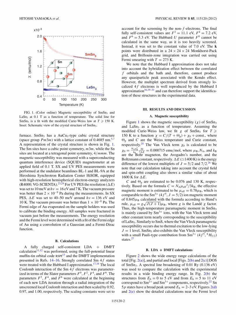
FIG. 1. (Color online) Magnetic susceptibility of SmSn3 andLaSn3 at 0.1 T as a function of temperature. The solid line forSmSn3 is a fit with the modified Curie-Weiss law at T � 150 K.Inset: Schematic view of the crystal structure of SmSn3.
furnace. SmSn3 has a AuCu3-type cubic crystal structure(space group Pm3m) with a lattice constant of 0.4685 nm.5,7
A representation of the crystal structure is shown in Fig. 1.The Sm sites have a cubic point symmetry, m3m, while the Snsites are located at a tetragonal point symmetry, 4/mmm. Themagnetic susceptibility was measured with a superconductingquantum interference device (SQUID) magnetometer at anapplied field of 0.1 T. SX and UV PES measurements wereperformed at the undulator beamlines BL-1 and BL-9A at theHiroshima Synchrotron Radiation Center HiSOR, equippedwith high-resolution hemispherical electron-energy analyzers(R4000; VG-SCIENTA).23,24 For UV PES the resolution (�E)was set to 10 meV at hν = 16 eV and 7 K. The vacuum pressurewas better than 2 × 10⁻⁹ Pa during the measurements. In SXPES, �E was set to 40–50 meV around hν = 136 eV and10 K. The vacuum pressure was better than 1 × 10⁻⁸ Pa. TheFermi edge of Au evaporated on the sample holders was usedto calibrate the binding energy. All samples were fractured invacuum just before the measurements. The energy resolutionand the Fermi level were determined with a fit of the Fermi edgeof Au using a convolution of a Gaussian and a Fermi-Diracfunction.
B. Calculations
A fully charged self-consistent LDA + DMFTcalculation11,12 was performed, using the full-potential linearmuffin-tin orbital code RSPt13 and the DMFT implementationpresented in Refs. 14–16. Strongly correlated Sm 4f stateswere treated with the Hubbard I approximation.17,18 The localCoulomb interaction of the Sm 4f electrons was parameter-ized in terms of the Slater parameters F 0, F 2, F 4, and F 6. Theparameters F 2, F 4, and F 6 were calculated at the beginningof each new LDA iteration through a radial integration of theunscreened local Coulomb interaction and then scaled by 0.92,0.97, and 1.00, respectively. The scaling constants were set to
account for the screening by the non-f -electrons. The finalfully self-consistent values are F 2 = 11.1 eV, F 4 = 7.2 eV,and F 6 = 5.3 eV. The Hubbard U parameter F 0 cannot becalculated in the same way, as it is too heavily screened.Instead, it was set to the constant value of 7.0 eV. The kpoints were distributed in a 24 × 24 × 24 Monkhorst-Packgrid, and Brillouin-zone integration was carried out usingFermi smearing with T = 273 K.
We note that the Hubbard I approximation does not takeinto account the hybridization effect between the correlatedf orbitals and the bath and, therefore, cannot produceany quasiparticle peak associated with the Kondo effect.However, the multiplet spectrum derived from strongly lo-calized 4f electrons is well reproduced by the Hubbard Iapproximation16,19–21 and can therefore support the identifica-tion of these structures in the experimental data.
III. RESULTS AND DISCUSSION
A. Magnetic susceptibility
Figure 1 shows the magnetic susceptibility (χ ) of SmSn3
and LaSn3 as a function of temperature. Assuming themodified Curie-Weiss law, we fit χ of SmSn3 for T �150 K to a function χ = C/(T + �p) + χ0 + const., where�p and C are the Weiss temperature and Curie constant,respectively.25 The Van Vleck term χ0 is calculated to be
χ0 = NAμ2B
kB
207�E
= 0.000715 emu/mol, where μB,NA, and kB
are the Bohr magneton, the Avogadro’s number, and theBoltzmann constant, respectively. �E (�1400 K) is the energydifference of the lowest multiplets of J = 5/2 and 7/2.26 Wenote that our calculation taking into account the crystal fieldand spin-orbit coupling also shows a similar value of about1600 K for �E.
C and �p are estimated to be 0.076 and 130 K, respec-tively. Based on the formula C = NAμeff
2/3kB, the effectivemagnetic moment is estimated to be μeff = 0.78μB, which iscomparable to the Sm3+ (4f 5, J = 5/2) ion magnetic momentof 0.845μB calculated with the formula according to Hund’srule, μeff = g
√J (J + 1)μB, where g is the Lande g factor.
Thus, the high-temperature paramagnetic moment in SmSn3
is mainly caused by Sm3+ ions, with the Van Vleck term andother constant term nearly corresponding to the susceptibilityof LaSn3. Similarly to SmS, where the Van Vleck paramagneticsusceptibility occurs due to thermal excitation to the low-lyingJ = 1 level, SmSn3 also exhibits the Van Vleck susceptibilitywith a small Pauli-type contribution from Sm3+ (4f 5, 6H5/2)states.27
B. LDA + DMFT calculations
Figure 2 shows the wide energy range calculations of thetotal [Fig. 2(a)], and partial and local [Figs. 2(b) and 2(c)] DOSof SmSn3. A spectral line broadening of 0.01 Ry (0.136 eV)was used to compare the calculation with the experimentalresults in a wide binding energy range. In Fig. 2(b) thestructures from Eb = 0 to 5 eV and from Eb = 5 to 11 eVcorrespond to Sm2+ and Sm3+ components, respectively.22 Sn5p states have a broad peak around Eb = 2–3 eV. Figures 2(d)and 2(e) show the detailed calculations near the Fermi level
115120-2
HIGH-RESOLUTION PHOTOELECTRON SPECTROSCOPY . . . PHYSICAL REVIEW B 85, 115120 (2012)
0
2
4
6
SmSn 3
TotalDOS
0
1
10 5 0 -5 -10
Sn 5d x3Sn 5p x3Sn 5s x3
Sn DOS
0
4
8
12 Sm 4fSm 5dSm 6pSm 6s
Sm 2+ DOS
0
1
2
1.5 1.0 0.5 0 0.5 -1.0 -1.5
Sn 5d x3Sn 5p x3Sn 5s x3
Sn DOS
Binding energy (eV)
0
2
4
Sm 4fSm 5dSm 6pSm 6s
Sm 3+ Sm 2+
6H
6F
6P
5I
5F
5G
5D
Sm DOS
(a)
(b)
(d)
(c)
(e)
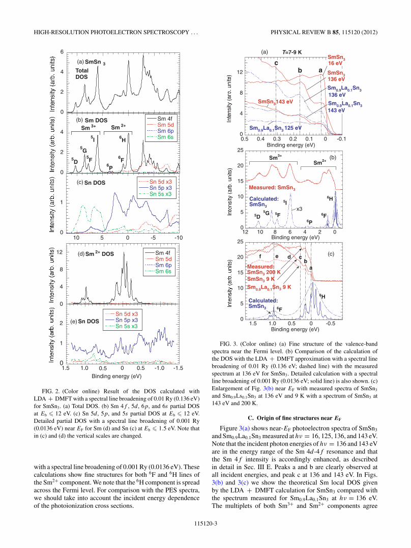
FIG. 2. (Color online) Result of the DOS calculated withLDA + DMFT with a spectral line broadening of 0.01 Ry (0.136 eV)for SmSn3. (a) Total DOS. (b) Sm 4f , 5d , 6p, and 6s partial DOSat Eb � 12 eV. (c) Sn 5d , 5p, and 5s partial DOS at Eb � 12 eV.Detailed partial DOS with a spectral line broadening of 0.001 Ry(0.0136 eV) near EF for Sm (d) and Sn (c) at Eb � 1.5 eV. Note thatin (c) and (d) the vertical scales are changed.
with a spectral line broadening of 0.001 Ry (0.0136 eV). Thesecalculations show fine structures for both 6F and 6H lines ofthe Sm2+ component. We note that the 6H component is spreadacross the Fermi level. For comparison with the PES spectra,we should take into account the incident energy dependenceof the photoionization cross sections.
0.5 0.4 0.3 0.2 0.1 0 -0.10
4
8
12
Binding energy (eV)
abc
SmSn3143 eV
T=7-9 K
125 eVSm0.9La0.1Sn3
143 eVSm0.9La0.1Sn3
SmSn316 eV
136 eVSmSn3
Sm0.9La0.1Sn3136 eV
0
5
10
15
20
25
12 10 8 6 4 2 0Binding energy (eV)
Measured: SmSn3
6H
6F
Calculated: SmSn3
6P
5I
5F5G5D
Sm3+
Sm2+
x3
0
5
10
15
20
25
1.5 1.0 0.5 0 -0.5Binding energy (eV)
Measured: SmSn3 200 KSmSn3 9 KSm0.9La0.1Sn3 9 K
6H
6F
ab
cdef
Calculated: SmSn3
(a)
(b)
(c)
FIG. 3. (Color online) (a) Fine structure of the valence-bandspectra near the Fermi level. (b) Comparison of the calculation ofthe DOS with the LDA + DMFT approximation with a spectral linebroadening of 0.01 Ry (0.136 eV; dashed line) with the measuredspectrum at 136 eV for SmSn3. Detailed calculation with a spectralline broadening of 0.001 Ry (0.0136 eV; solid line) is also shown. (c)Enlargement of Fig. 3(b) near EF with measured spectra of SmSn3
and Sm0.9Ls0.1Sn3 at 136 eV and 9 K with a spectrum of SmSn3 at143 eV and 200 K.
C. Origin of fine structures near EF
Figure 3(a) shows near-EF photoelectron spectra of SmSn3
and Sm0.9La0.1Sn3 measured at hν = 16, 125, 136, and 143 eV.Note that the incident photon energies of hν = 136 and 143 eVare in the energy range of the Sm 4d-4f resonance and thatthe Sm 4f intensity is accordingly enhanced, as describedin detail in Sec. III E. Peaks a and b are clearly observed atall incident energies, and peak c at 136 and 143 eV. In Figs.3(b) and 3(c) we show the theoretical Sm local DOS givenby the LDA + DMFT calculation for SmSn3 compared withthe spectrum measured for Sm0.9La0.1Sn3 at hν = 136 eV.The multiplets of both Sm3+ and Sm2+ components agree
115120-3

HITOSHI YAMAOKA et al. PHYSICAL REVIEW B 85, 115120 (2012)
very well with the calculated SmSn3 spectrum as shown inFigs. 3(b) and 3(c), respectively. The detailed comparison inFig. 3(c) allows us to identify the peaks in the experimentalspectrum labeled a, b, c, and e as bulk 6H and 6F componentsof Sm2+, respectively.22 To our knowledge, UV and SX-PESspectra with resolved bulk components have not been reportedfor a Sm compound so far. In the detailed calculation theenergy separation between peaks a, b, and c is of the order of0.13 eV, which is much larger than the experimental energyresolution and, therefore, explains why we were able to clearlyresolve them.
Based on the results of the first principle calculations,29theenergy shifts of the surface components from the bulk onesshould be 0.4–0.5 eV. Thus the broad peaks labeled d and f areprobably derived from the surface contributions, similarly towhat we previously observed in Yb compounds.28 Accordingto the calculated spectrum in Fig. 3(b), the 6P componentsof Sm2+ are expected to appear within an electron bindingenergy range of Eb = 3–4 eV. Based on the fact that thecalculated 6P features have a very weak intensity, we canreasonably consider that the broad peak observed in theexperimental spectrum around Eb = 4 eV mostly correspondsto the surface contribution of 6P. We additionally note that theenergy difference between the d and the f peaks is about 20%smaller than that between a and e, which reflects the differentchemical environment.
D. Temperature dependence of the electronic structure near EF
Figure 4(a) shows the temperature-dependent high-resolution valence-band spectra of SmSn3 measured at hν =16 eV. We observe two distinct features, which correspondto peaks a and b in Fig. 3. We note that in this incidentphoton energy range the photoionization cross section of 4f
is one order smaller than that of Sn 5p,30 which results in aweaker contribution of the Sm2+ 4f states to the valence-bandspectrum than the spectra measured at hν = 136 and 143 eV.
The temperature dependence of the DOS of SmSn3 de-rived by dividing the valence-band spectra with a Gaussian-broadened Fermi-Dirac distribution is plotted in Fig. 4(b).One may examine the DOS down to −5kBT .31 A finiteDOS exists from room temperature down to 6.8 K, whichreflects the metallic character of SmSn3. A V-shaped gap
0
1
2
3
0.3 0.2 0.1 0 -0.1Binding energy (eV)
SmSn3 hν=16 eV
250 K200 K150 K100 K80 K60 K40 K20 K
6.8 K
ab
0
1
2
0.4 0.2 0 -0.2
6.8 K20 K40 K60 K80 K100 K150 K200 K250 K
Binding energy (eV)
SmSn3 hν=16 eV
Intr
ensi
ty (
arb.
uni
ts)
Intr
ensi
ty (
arb.
uni
ts)
ab
(a) (b)
FIG. 4. (Color online) (a) Temperature dependence of valence-band spectra for SmSn3 at hν = 16 eV. Two distinct peaks are labeleda and b. (b) Density of states near the Fermi level.
structure is observed just above the Fermi level in the entiremeasured temperature range. In SmSn3 the ground state isa �8 quadruplet and the energy difference between �8 andthe �7 doublet is about 50 K.32 Our calculation also gives asimilar value of 45 K for the energy difference between �8
and �7. The stable gap position below 60 K in SmSn3 likelycorresponds to the fact that the system is in the �8 groundstate. Both the gap width and the binding energy of peak adecrease monotonically with decreasing temperature. Whereasthe decrease in the gap at low temperatures is reminiscent ofthe metallic phase of FeSi before the transition to the insulatorstate,33 the resistivity of SmSn3 does rapidly decrease at lowtemperatures, ruling out a metal-to-insulator transition. Thereshould exist a hybridization between the Sm 4f and the Sn5p states. However, the Hubbard I approximation used in theLDA + DMFT calculation neglects this hybridization, sofurther theoretical study may be necessary to understand thetemperature dependence of the DOS near EF.
As mentioned above, the specific heat was reported to showa broad peak at 10.8 K and two sharp peaks at 9.3 and 9.6 K.5
The two sharp peaks below TN have been suggested to originatefrom multiple magnetic order such as quadrupole order.34
Recently, a zero-field muon spin relaxation measurement forthe analogue compound SmIn3, which also showed anomaliesin the specific heat at 16.5, 15.1, and 14.7 K,5 indicatedthat the primary order parameters in all the ordered phaseswere magnetic, though the results were in contrast to thepure quadrupole ordering scenario.34 Our PES data show littledifference in the valence-band spectra between T = 6.8 andT = 20 K. This indicates that the electronic structure at EF
does not change significantly below 60 K.
E. Incident energy dependence
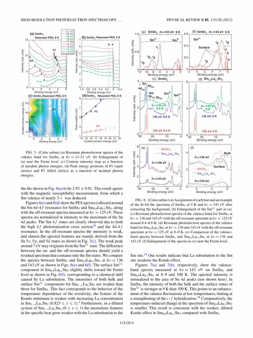
Figures 5(a) and 5(b) show the valence-band spectra forEb � 9 eV and near the Fermi level, respectively, at hν = 13–21 eV. Figure 5(c) exhibits the contour intensity map of thespectra. We observe two kinds of peak features, labeled P1 andP2 in Fig. 5(a), which shift with the incident photon energies,while peaks a and b in Fig. 5(b) stay at a constant bindingenergy. As shown in Fig. 5(d) the energy of peak P2 showsa linear, slope 1 shift with the incident energy; we thereforeassign it to the resonant Auger component. On the other hand,the incident energy dependence of the binding energy of peakP1 is much weaker.
We performed resonant PES28,35 for incident photon ener-gies of 136 and 143 eV. Figures 6(a) and 6(b) show examples ofthe fit of the valence-band spectrum of SmSn3 at hν = 143 eVafter subtracting the background. It is known that in theincident photon energy range of the Sm 4d-4f resonance,the Sm2+ component mainly originates from the surface layer.Consequently, the Sm2+ surface state is probed at these photonenergies,36,37 whereas the Sm3+ component is considered tobe from the bulk even at these incident energies. At the surfacethe Sm atoms are less coordinated; their cohesive energy istherefore lower than that of the bulk Sm atoms, which resultsin the surface Sm atoms tending to be in the divalent state.However, in our high-resolution measurement we successfullyseparated a small bulk component of Sm2+, as illustrated inFig. 6(f). The bulk valence of SmSn3 at 9 K is estimated from
115120-4
HIGH-RESOLUTION PHOTOELECTRON SPECTROSCOPY . . . PHYSICAL REVIEW B 85, 115120 (2012)
8 6 4 2 0
20
18
16
14
Binding energy (eV)
Inci
dent
pho
ton
ener
gy (
eV)
(c) SmSn Resonant PES, 8 K3
1
3
5
7
9
14 15 16 17 18 19 20 21 22Incident photon energy (eV)
P1
P2
(d)SmSn3 Resonant PES, 8 K
Pea
k po
sitio
n (e
V)P1
P2
Inte
nsity
(ar
b. u
nits
)
Inte
nsity
(ar
b. u
nits
)
0
5
10
15
8 6 4 2 0
21 eV20 eV19 eV18 eV17 eV16 eV15 eV14 eV13 eV
Binding energy (eV)
SmSn3 Resonant PES, 8 K
P1
P2
(a)
0
1
2
3
4
5
6
7
1.0 0.8 0.6 0.4 0.2 0 -0.2Binding energy (eV)
SmSn3(b) Resonant PES, 8 K
ab
FIG. 5. (Color online) (a) Resonant photoelectron spectra of thevalence band for SmSn3 at hν = 13–21 eV. (b) Enlargement of(a) near the Fermi level. (c) Contour intensity map as a functionof incident photon energies. (d) Peak energy positions of P1 (opencircles) and P2 (filled circles) as a function of incident photonenergies.
the fits shown in Fig. 6(a) to be 2.93 ± 0.01. This result agreeswith the magnetic susceptibility measurement, from which aSm valence of nearly 3 + was deduced.
Figures 6(c) and 6(d) show the PES spectra collected aroundthe Sm 4d-4f resonance for SmSn3 and Sm0.9La0.1Sn3, alongwith the off-resonant spectra measured at hν = 125 eV. Thesespectra are normalized in intensity to the maximum of the Sn4d peaks. The Sm 4f states are clearly observed due to boththe high 4f photoionization cross section30 and the 4d-4f
resonance. In the off-resonant spectra the intensity is weak,and almost-flat spectral features are mainly derived from theSn 5s, 5p, and 5d states as shown in Fig. 2(c). The weak peakaround 7 eV may originate from the Sm3+ state. The differencebetween the on- and the off-resonant spectra should yield aresidual spectrum that contains only the Sm states. We comparethe spectra between SmSn3 and Sm0.9La0.1Sn3 at hν = 136and 143 eV as shown in Figs. 6(e) and 6(f). The surface Sm2+component in Sm0.9La0.1Sn3 slightly shifts toward the Fermilevel as shown in Fig. 6(f), corresponding to a chemical shiftcaused by La substitution. The intensities of both bulk andsurface Sm2+ components for Sm1−xLaxSn3 are weaker thanthose for SmSn3. This fact corresponds to the behavior of thetemperature dependence of the resistivity; the feature of theKondo minimum is weaker with increasing La concentrationin Sm1−xLaxSn3 (0.823 � x � 1).4 Furthermore, in a dilutedsystem of Sm1−xLaxSn3 (0 � x � 1) the anomalous featuresin the specific heat grew weaker with the La substitution to the
Inte
nsity
(ar
b. u
nits
)In
tens
ity (
arb.
uni
ts)
Inte
nsity
(ar
b. u
nits
)0
4
8
20 10 0Binding energy (eV)
Sm0.9La0.1Sn3
hν=143 eV, 8 K
136 eV, 9 K
125 eV, 9 K
300
2
4
20 10 0Binding energy (eV)
SmSn3
hν=143 eV, 8.5 K
136 eV, 8.6 K
125 eV, 8.4 K
Sn4d5/2
Sm5p3/2
5p1/2
Sm3+
Sm2+
4d3/2
30
0
2
4
6
8
30 20 10 0
SmSn3
Sm0.9La0.1Sn3
Binding energy (eV)
hν=136 eV
hν=143 eV
0
2
4
4 2 0
SmSn3
Sm0.9La0.1Sn3
Binding energy (eV)
hν=136 eV
hν=143 eV
Surface
Bulk
0
0.8
1.6
12 10 8 6 4 2 0Binding energy (eV)
SmSn3 hν=143 eV 9 K
Sm3+
5I
5F5G
5D
Sm2+
a
b
6P
6F6H
cSurface
Sm2+
0
0.2
0.4
0.6
5 4 3 2 1 0Binding energy (eV)
SmSn3 hν=143 eV 9 K(a) (b)
(c) (d)
(e) (f)
FIG. 6. (Color online) (a) Assignment of each line and an exampleof the fit for the spectrum of SmSn3 at 9 K and hν = 143 eV afterextracting the background. (b) Enlargement of the Sm2+ part in (a).(c) Resonant photoelectron spectra of the valence band for SmSn3 athν = 136 and 143 eV with the off-resonant spectrum at hν = 125 eVaround 8.4–8.6 K. (d) Resonant photoelectron spectra of the valenceband for Sm0.9La0.1Sn3 at hν = 136 and 143 eV with the off-resonantspectrum at hν = 125 eV at 8–9 K. (e) Comparison of the valence-band spectra between SmSn3 and Sm0.9La0.1Sn3 at hν = 136 and143 eV. (f) Enlargement of the spectra in (e) near the Fermi level.
Sm site.10 Our results indicate that La substitution to the Smsite weakens the Kondo effect.
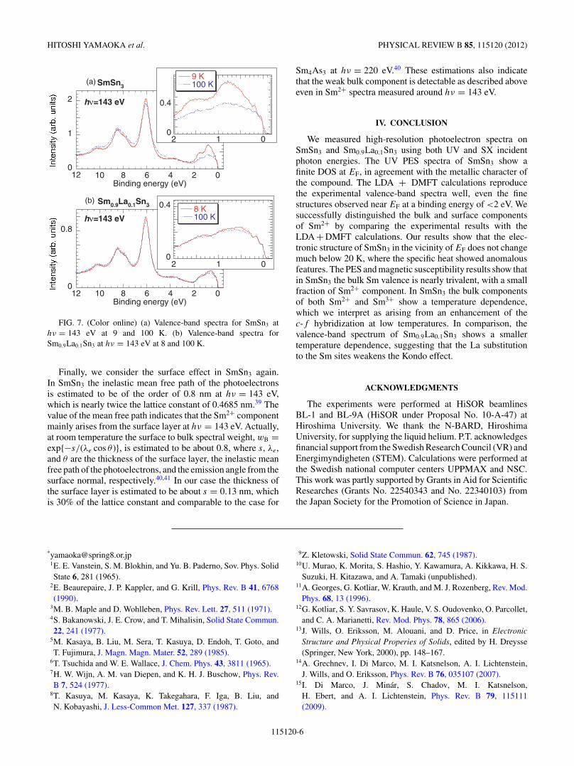
Figures 7(a) and 7(b), respectively, show the valence-band spectra measured at hν = 143 eV on SmSn3 andSm0.9La0.1Sn3 at 8–9 and 100 K. The spectral intensity isnormalized to the area of Sn 4d peaks (not shown here). InSmSn3 the intensity of both the bulk and the surface states ofSm2+ is stronger at 9 K than 100 K. This points to an enhance-ment of the valence fluctuations at low temperatures, hinting ata strengthening of the c-f hybridization.38 Comparatively, thetemperature-induced change in the spectrum of Sm0.9La0.1Sn3
is smaller. This result is consistent with the weaker, dilutedKondo effect in Sm0.9La0.1Sn3 compared with SmSn3.
115120-5
HITOSHI YAMAOKA et al. PHYSICAL REVIEW B 85, 115120 (2012)
0
1
2
12 10 8 6 4 2 0Binding energy (eV)
SmSn3
hν=143 eV
0
0.4
2 1 0
9 K100 K
0
0.8
12 10 8 6 4 2 0Binding energy (eV)
Sm0.9La0.1Sn3
hν=143 eV
0
0.4
2 1 0
8 K100 K
(b)
(a)
FIG. 7. (Color online) (a) Valence-band spectra for SmSn3 athν = 143 eV at 9 and 100 K. (b) Valence-band spectra forSm0.9La0.1Sn3 at hν = 143 eV at 8 and 100 K.
Finally, we consider the surface effect in SmSn3 again.In SmSn3 the inelastic mean free path of the photoelectronsis estimated to be of the order of 0.8 nm at hν = 143 eV,which is nearly twice the lattice constant of 0.4685 nm.39 Thevalue of the mean free path indicates that the Sm2+ componentmainly arises from the surface layer at hν = 143 eV. Actually,at room temperature the surface to bulk spectral weight, wB =exp{−s/(λe cos θ )}, is estimated to be about 0.8, where s, λe,and θ are the thickness of the surface layer, the inelastic meanfree path of the photoelectrons, and the emission angle from thesurface normal, respectively.40,41 In our case the thickness ofthe surface layer is estimated to be about s = 0.13 nm, whichis 30% of the lattice constant and comparable to the case for
Sm4As3 at hν = 220 eV.40 These estimations also indicatethat the weak bulk component is detectable as described aboveeven in Sm2+ spectra measured around hν = 143 eV.
IV. CONCLUSION
We measured high-resolution photoelectron spectra onSmSn3 and Sm0.9La0.1Sn3 using both UV and SX incidentphoton energies. The UV PES spectra of SmSn3 show afinite DOS at EF, in agreement with the metallic character ofthe compound. The LDA + DMFT calculations reproducethe experimental valence-band spectra well, even the finestructures observed near EF at a binding energy of <2 eV. Wesuccessfully distinguished the bulk and surface componentsof Sm2+ by comparing the experimental results with theLDA + DMFT calculations. Our results show that the elec-tronic structure of SmSn3 in the vicinity of EF does not changemuch below 20 K, where the specific heat showed anomalousfeatures. The PES and magnetic susceptibility results show thatin SmSn3 the bulk Sm valence is nearly trivalent, with a smallfraction of Sm2+ component. In SmSn3 the bulk componentsof both Sm2+ and Sm3+ show a temperature dependence,which we interpret as arising from an enhancement of thec-f hybridization at low temperatures. In comparison, thevalence-band spectrum of Sm0.9La0.1Sn3 shows a smallertemperature dependence, suggesting that the La substitutionto the Sm sites weakens the Kondo effect.
ACKNOWLEDGMENTS
The experiments were performed at HiSOR beamlinesBL-1 and BL-9A (HiSOR under Proposal No. 10-A-47) atHiroshima University. We thank the N-BARD, HiroshimaUniversity, for supplying the liquid helium. P.T. acknowledgesfinancial support from the Swedish Research Council (VR) andEnergimyndigheten (STEM). Calculations were performed atthe Swedish national computer centers UPPMAX and NSC.This work was partly supported by Grants in Aid for ScientificResearches (Grants No. 22540343 and No. 22340103) fromthe Japan Society for the Promotion of Science in Japan.
*[email protected]. E. Vanstein, S. M. Blokhin, and Yu. B. Paderno, Sov. Phys. SolidState 6, 281 (1965).
2E. Beaurepaire, J. P. Kappler, and G. Krill, Phys. Rev. B 41, 6768(1990).
3M. B. Maple and D. Wohlleben, Phys. Rev. Lett. 27, 511 (1971).4S. Bakanowski, J. E. Crow, and T. Mihalisin, Solid State Commun.22, 241 (1977).
5M. Kasaya, B. Liu, M. Sera, T. Kasuya, D. Endoh, T. Goto, andT. Fujimura, J. Magn. Magn. Mater. 52, 289 (1985).
6T. Tsuchida and W. E. Wallace, J. Chem. Phys. 43, 3811 (1965).7H. W. Wijn, A. M. van Diepen, and K. H. J. Buschow, Phys. Rev.B 7, 524 (1977).
8T. Kasuya, M. Kasaya, K. Takegahara, F. Iga, B. Liu, andN. Kobayashi, J. Less-Common Met. 127, 337 (1987).
9Z. Kletowski, Solid State Commun. 62, 745 (1987).10U. Murao, K. Morita, S. Hashio, Y. Kawamura, A. Kikkawa, H. S.
Suzuki, H. Kitazawa, and A. Tamaki (unpublished).11A. Georges, G. Kotliar, W. Krauth, and M. J. Rozenberg, Rev. Mod.
Phys. 68, 13 (1996).12G. Kotliar, S. Y. Savrasov, K. Haule, V. S. Oudovenko, O. Parcollet,
and C. A. Marianetti, Rev. Mod. Phys. 78, 865 (2006).13J. Wills, O. Eriksson, M. Alouani, and D. Price, in Electronic
Structure and Physical Properies of Solids, edited by H. Dreysse(Springer, New York, 2000), pp. 148–167.
14A. Grechnev, I. Di Marco, M. I. Katsnelson, A. I. Lichtenstein,J. Wills, and O. Eriksson, Phys. Rev. B 76, 035107 (2007).
15I. Di Marco, J. Minar, S. Chadov, M. I. Katsnelson,H. Ebert, and A. I. Lichtenstein, Phys. Rev. B 79, 115111(2009).
115120-6

HIGH-RESOLUTION PHOTOELECTRON SPECTROSCOPY . . . PHYSICAL REVIEW B 85, 115120 (2012)
16P. Thunstrom, I. Di Marco, A. Grechnev, S. Lebegue, M. I.Katsnelson, A. Svane, and O. Eriksson, Phys. Rev. B 79, 165104(2009).
17J. Hubbard, Proc. R. Soc. London Ser. A 276, 238 (1963).18A. I. Lichtenstein and M. I. Katsnelson, Phys. Rev. B 57, 6884
(1998).19S. Lebegue, G. Santi, A. Svane, O. Bengone, M. I. Katsnelson,
A. I. Lichtenstein, and O. Eriksson, Phys. Rev. B 72, 245102 (2005).20S. Lebegue, A. Svane, M. I. Katsnelson, A. I. Lichtenstein, and
O. Eriksson, J. Phys. Condens. Matter 18, 6329 (2006).21O. Granas, I. Di Marco, P. Thunstrom, L. Nordstrom, O. Eriksson,
T. Bjorkman, and J. M. Wills, Comput. Mater. Sci. 55, 295 (2012).22M. Campagna, E. Bucher, G. K. Wertheim, and L. D. Longinotti,
Phys. Rev. Lett. 33, 165 (1974).23K. Shimada, M. Arita, Y. Takeda, H. Fujino, K. Kobayashi,
T. Narimura, H. Namatame, and M. Taniguchi, Surf. Rev. Lett.9, 529 (2002).
24M. Arita, K. Shimada, Y. Takeda, M. Nakatake, H. Namatame, andM. Taniguchi, Surf. Rev. Lett. 9, 535 (2002).
25A. M. Stewart, Phys. Rev. B 6, 1985 (1972).26S. K. Malik, Phys. Lett. A 31, 33 (1970).27J. M. Lawrence, P. S. Riseborough, and R. D. Parks, Rep. Prog.
Phys. 44, 1 (1981).28H. Yamaoka, I. Jarrige, N. Tsujii, M. Imai, J.-F. Lin,
M. Matsunami, R. Eguchi, M. Arita, K. Shimada, H. Namatame,M. Taniguchi, M. Taguchi, Y. Senba, H. Ohashi, N. Hiraoka,H. Ishii, and K.-D. Tsuei, Phys. Rev. B 83, 104525 (2011).
29M. Alden, B. Johansson, and H. L. Skriver, Phys. Rev. B 51, 5386(1995).
30J. J. Yeh and I. Lindau, At. Data Nucl. Data Tables 32, 1 (1985).31T. Greber, T. J. Kreutz, and J. Osterwalder, Phys. Rev. Lett. 79,
4465 (1997).32D. Endoh, T. Goto, A. Tamaki, B. Liu, M. Kasaya, T. Fujimura, and
T. Kasuya, J. Phys. Soc. Jpn. 58, 940 (1989).33M. Arita, K. Shimada, Y. Takeda, M. Nakatake, H. Namatame,
M. Taniguchi, H. Negishi, T. Oguchi, T. Saitoh, A. Fujimori, andT. Kanomata, Phys. Rev. B 77, 205117 (2008).
34T. U. Ito, W. Higemoto, K. Ninomiya, H. Luetkens, T. Sugai,Y. Haga, and H. Suzuki, J. Phys. Soc. Jpn. 80, 033710 (2011).
35H. Yamaoka, M. Matsunami, R. Eguchi, Y. Ishida, N. Tsujii,Y. Takahashi, Y. Senba, H. Ohashi, and S. Shin, Phys. Rev. B 78,045125 (2008).
36E. Vescovo, R. Rochow, T. Kachel, and C. Carbone, Phys. Rev. B46, 4788 (1992).
37G. Kutluk, M. Nakatake, H. Sumuda, H. Namatame, andM. Taniguchi, Surf. Interf. Anal. 42, 712 (2010).
38H. Yamaoka, I. Jarrige, N. Tsujii, J.-F. Lin, N. Hiraoka, H. Ishii,and K.-D. Tsuei, Phys. Rev. B 82, 035111 (2010).
39M. P. Seah and W. A. Dench, Surf. Interf. Anal. 1, 2 (1979).40A. Yamasaki, A. Sekiyama, S. Imada, M. Tsunekawa, C. Dallera,
L. Braicovich, T.-L. Lee, A. Ochiai, and S. Suga, J. Phys. Soc. Jpn.74, 2538 (2005).
41G. K. Wertheim and G. Grecelius, Phys. Rev. Lett. 40, 813(1978).
115120-7
Copyright © 2022 FDOKUMEN