High-performance and Power-efficient Computing with MRAM ...
14
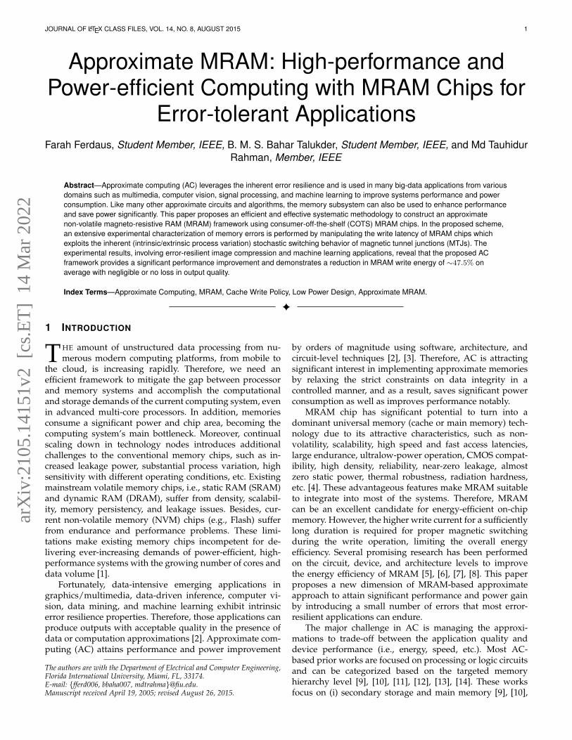
JOURNAL OF L A T E X CLASS FILES, VOL. 14, NO. 8, AUGUST 2015 1 Approximate MRAM: High-performance and Power-efficient Computing with MRAM Chips for Error-tolerant Applications Farah Ferdaus, Student Member, IEEE, B. M. S. Bahar Talukder, Student Member, IEEE, and Md Tauhidur Rahman, Member, IEEE Abstract—Approximate computing (AC) leverages the inherent error resilience and is used in many big-data applications from various domains such as multimedia, computer vision, signal processing, and machine learning to improve systems performance and power consumption. Like many other approximate circuits and algorithms, the memory subsystem can also be used to enhance performance and save power significantly. This paper proposes an efficient and effective systematic methodology to construct an approximate non-volatile magneto-resistive RAM (MRAM) framework using consumer-off-the-shelf (COTS) MRAM chips. In the proposed scheme, an extensive experimental characterization of memory errors is performed by manipulating the write latency of MRAM chips which exploits the inherent (intrinsic/extrinsic process variation) stochastic switching behavior of magnetic tunnel junctions (MTJs). The experimental results, involving error-resilient image compression and machine learning applications, reveal that the proposed AC framework provides a significant performance improvement and demonstrates a reduction in MRAM write energy of ∼47.5% on average with negligible or no loss in output quality. Index Terms—Approximate Computing, MRAM, Cache Write Policy, Low Power Design, Approximate MRAM. ✦ 1 I NTRODUCTION T HE amount of unstructured data processing from nu- merous modern computing platforms, from mobile to the cloud, is increasing rapidly. Therefore, we need an efficient framework to mitigate the gap between processor and memory systems and accomplish the computational and storage demands of the current computing system, even in advanced multi-core processors. In addition, memories consume a significant power and chip area, becoming the computing system’s main bottleneck. Moreover, continual scaling down in technology nodes introduces additional challenges to the conventional memory chips, such as in- creased leakage power, substantial process variation, high sensitivity with different operating conditions, etc. Existing mainstream volatile memory chips, i.e., static RAM (SRAM) and dynamic RAM (DRAM), suffer from density, scalabil- ity, memory persistency, and leakage issues. Besides, cur- rent non-volatile memory (NVM) chips (e.g., Flash) suffer from endurance and performance problems. These limi- tations make existing memory chips incompetent for de- livering ever-increasing demands of power-efficient, high- performance systems with the growing number of cores and data volume [1]. Fortunately, data-intensive emerging applications in graphics/multimedia, data-driven inference, computer vi- sion, data mining, and machine learning exhibit intrinsic error resilience properties. Therefore, those applications can produce outputs with acceptable quality in the presence of data or computation approximations [2]. Approximate com- puting (AC) attains performance and power improvement The authors are with the Department of Electrical and Computer Engineering, Florida International University, Miami, FL, 33174. E-mail: {fferd006, bbaha007, mdtrahma}@fiu.edu. Manuscript received April 19, 2005; revised August 26, 2015. by orders of magnitude using software, architecture, and circuit-level techniques [2], [3]. Therefore, AC is attracting significant interest in implementing approximate memories by relaxing the strict constraints on data integrity in a controlled manner, and as a result, saves significant power consumption as well as improves performance notably. MRAM chip has significant potential to turn into a dominant universal memory (cache or main memory) tech- nology due to its attractive characteristics, such as non- volatility, scalability, high speed and fast access latencies, large endurance, ultralow-power operation, CMOS compat- ibility, high density, reliability, near-zero leakage, almost zero static power, thermal robustness, radiation hardness, etc. [4]. These advantageous features make MRAM suitable to integrate into most of the systems. Therefore, MRAM can be an excellent candidate for energy-efficient on-chip memory. However, the higher write current for a sufficiently long duration is required for proper magnetic switching during the write operation, limiting the overall energy efficiency. Several promising research has been performed on the circuit, device, and architecture levels to improve the energy efficiency of MRAM [5], [6], [7], [8]. This paper proposes a new dimension of MRAM-based approximate approach to attain significant performance and power gain by introducing a small number of errors that most error- resilient applications can endure. The major challenge in AC is managing the approxi- mations to trade-off between the application quality and device performance (i.e., energy, speed, etc.). Most AC- based prior works are focused on processing or logic circuits and can be categorized based on the targeted memory hierarchy level [9], [10], [11], [12], [13], [14]. These works focus on (i) secondary storage and main memory [9], [10], arXiv:2105.14151v2 [cs.ET] 14 Mar 2022
-
Upload
khangminh22 -
Category
Documents
-
view
0 -
download
0
Transcript of High-performance and Power-efficient Computing with MRAM ...
JOURNAL OF LATEX CLASS FILES, VOL. 14, NO. 8, AUGUST 2015 1
Approximate MRAM: High-performance andPower-efficient Computing with MRAM Chips for
Error-tolerant ApplicationsFarah Ferdaus, Student Member, IEEE, B. M. S. Bahar Talukder, Student Member, IEEE, and Md Tauhidur
Rahman, Member, IEEE
Abstract—Approximate computing (AC) leverages the inherent error resilience and is used in many big-data applications from variousdomains such as multimedia, computer vision, signal processing, and machine learning to improve systems performance and powerconsumption. Like many other approximate circuits and algorithms, the memory subsystem can also be used to enhance performanceand save power significantly. This paper proposes an efficient and effective systematic methodology to construct an approximatenon-volatile magneto-resistive RAM (MRAM) framework using consumer-off-the-shelf (COTS) MRAM chips. In the proposed scheme,an extensive experimental characterization of memory errors is performed by manipulating the write latency of MRAM chips whichexploits the inherent (intrinsic/extrinsic process variation) stochastic switching behavior of magnetic tunnel junctions (MTJs). Theexperimental results, involving error-resilient image compression and machine learning applications, reveal that the proposed ACframework provides a significant performance improvement and demonstrates a reduction in MRAM write energy of ∼47.5% onaverage with negligible or no loss in output quality.
Index Terms—Approximate Computing, MRAM, Cache Write Policy, Low Power Design, Approximate MRAM.
F
1 INTRODUCTION
THE amount of unstructured data processing from nu-merous modern computing platforms, from mobile to
the cloud, is increasing rapidly. Therefore, we need anefficient framework to mitigate the gap between processorand memory systems and accomplish the computationaland storage demands of the current computing system, evenin advanced multi-core processors. In addition, memoriesconsume a significant power and chip area, becoming thecomputing system’s main bottleneck. Moreover, continualscaling down in technology nodes introduces additionalchallenges to the conventional memory chips, such as in-creased leakage power, substantial process variation, highsensitivity with different operating conditions, etc. Existingmainstream volatile memory chips, i.e., static RAM (SRAM)and dynamic RAM (DRAM), suffer from density, scalabil-ity, memory persistency, and leakage issues. Besides, cur-rent non-volatile memory (NVM) chips (e.g., Flash) sufferfrom endurance and performance problems. These limi-tations make existing memory chips incompetent for de-livering ever-increasing demands of power-efficient, high-performance systems with the growing number of cores anddata volume [1].
Fortunately, data-intensive emerging applications ingraphics/multimedia, data-driven inference, computer vi-sion, data mining, and machine learning exhibit intrinsicerror resilience properties. Therefore, those applications canproduce outputs with acceptable quality in the presence ofdata or computation approximations [2]. Approximate com-puting (AC) attains performance and power improvement
The authors are with the Department of Electrical and Computer Engineering,Florida International University, Miami, FL, 33174.E-mail: {fferd006, bbaha007, mdtrahma}@fiu.edu.Manuscript received April 19, 2005; revised August 26, 2015.
by orders of magnitude using software, architecture, andcircuit-level techniques [2], [3]. Therefore, AC is attractingsignificant interest in implementing approximate memoriesby relaxing the strict constraints on data integrity in acontrolled manner, and as a result, saves significant powerconsumption as well as improves performance notably.
MRAM chip has significant potential to turn into adominant universal memory (cache or main memory) tech-nology due to its attractive characteristics, such as non-volatility, scalability, high speed and fast access latencies,large endurance, ultralow-power operation, CMOS compat-ibility, high density, reliability, near-zero leakage, almostzero static power, thermal robustness, radiation hardness,etc. [4]. These advantageous features make MRAM suitableto integrate into most of the systems. Therefore, MRAMcan be an excellent candidate for energy-efficient on-chipmemory. However, the higher write current for a sufficientlylong duration is required for proper magnetic switchingduring the write operation, limiting the overall energyefficiency. Several promising research has been performedon the circuit, device, and architecture levels to improvethe energy efficiency of MRAM [5], [6], [7], [8]. This paperproposes a new dimension of MRAM-based approximateapproach to attain significant performance and power gainby introducing a small number of errors that most error-resilient applications can endure.
The major challenge in AC is managing the approxi-mations to trade-off between the application quality anddevice performance (i.e., energy, speed, etc.). Most AC-based prior works are focused on processing or logic circuitsand can be categorized based on the targeted memoryhierarchy level [9], [10], [11], [12], [13], [14]. These worksfocus on (i) secondary storage and main memory [9], [10],
arX
iv:2
105.
1415
1v2
[cs
.ET
] 1
4 M
ar 2
022
JOURNAL OF LATEX CLASS FILES, VOL. 14, NO. 8, AUGUST 2015 2
(ii) application-specific memory designs [11], [12], and (iii)CMOS memory-based approximate cache architecture [13],[14]. However, the existing MRAM-based AC framework ismostly simulation-based requires extension in either newinstruction set architecture (ISA) or enhancement in cachereplacement policies along with device-circuit-architectureremodeling [8], [12]. Hence, these MRAM-based AC frame-works can not be easily integrated into the existing comput-ing system due to the above-mentioned strict requirements.The previous contributions inspirit the need for real mem-ory implementation and build the foundation of the pro-posed MRAM-based AC framework using commercial-off-the-shelf (COTS) MRAM chips, which require minimal or noadditional hardware, is robust against operating conditions.To this end, we propose a system-level MRAM-based ex-perimental AC framework that works at the reduced writelatency of COTS MRAM chips to improve computationspeed significantly and energy efficiency with the cost ofsmall write accuracy.
This paper presents a new approach to constructingan approximate MRAM framework. We also introduce adata allocation scheme based on the cell characterizationalgorithm for the proposed framework. The core idea is thatat sub-optimal write latency, MRAM addresses can be splitinto accurate and approximate addresses through extensiveerror characterization of COTS toggle MRAM chips. Thecorrelation between the obtained errors and the application-level output quality guides the proper allocation of applica-tion data to MRAM addresses. The more straightforwardimplementation of the proposed mechanism results in abetter speed-power-quality trade-off. In summary, the keycontributions of this work are as follows.
• We reduce the write enable (W ) time from the manufac-turer’s recommended value during the write operation tointroduce errors. We extensively characterize these errorsusing COTS Everspin toggle MRAM chips [15] to improvewrite power efficiency by exploiting the applications’error-resilient nature. The characterization results are usedto derive key insights about memory errors — for exam-ple, toggling from “1”→ “0” and “0”→ “1” are mutuallyexclusive.
• Insights obtained from the characterization guide us inconstructing a systematic data allocation scheme basedon the application requirements to store critical and ap-proximate data considering the occurrence and propertiesof MRAM errors by writing different intuitive and non-intuitive input data patterns. Subsequently, approximatedata can be stored in the approximate addresses, whereascritical data must be allocated in entirely accurate memoryaddresses.
• We analyze a detailed trade-off between theapplication-level output accuracy and system-levelperformance/power gains by determining optimal writelatency.
• We implement our AC framework using our cus-tom memory controller implemented on Xilinx Artix 7(XC7A35T-1C) FPGA to manipulate different timing la-tency of a couple of emerging memories [16]. Our ex-perimental results show a significant improvement in thespeed-power-quality trade-off, an average write speed-up
of ∼29% and power savings of ∼47.5% with minimal orno loss in application quality.
The rest of the paper is organized as follows. Sect.2 provides an overview of related prior work. Sect. 3briefly overviews the organization and operating principleof MRAM chips and related preliminaries of cache writ-ing policies. Sect. 4 presents the proposed AC framework,including the cell characterization algorithm. Sect. 5 ex-plains the experimental setup and exhibits obtained results.Sect. 6 discusses the characterization and memory overheadrequired to store the erroneous memory addresses alongwith the proposed scheme’s applicability to next-generationMRAMs. Finally, Sect. 7 concludes the article.
2 RELATED WORK
This work correlates two distinct research areas – emergingMRAM memories with approximate computing. Previoussimulation-based MRAM-related work focuses on address-ing spintronic memories’ high write energy while pre-serving accurate read/write operations to achieve energy-efficient on-chip memories using the circuit, architectural,and device-level techniques [6], [17], [18], [19], [20], [21],[22]. In [17], using the bit-line voltage clamping technique,MRAM write-current asymmetry is mitigated at the cir-cuit level to achieve the goal. Besides, in [18], a co-designmethodology focusing on the bit-cell access transistor andthe supply voltage is proposed to improve energy efficiency.Moreover, the MRAM cell’s actual switching time detectiontechnique is proposed to cease the unnecessary current flowimmediately after a complete write [21]. Significant writeenergy reduction is achieved for such techniques; however,the overall write latency remains the same. On the otherhand, at the architectural level, in [19], [20], the proposed hy-brid CMOS-spintronic cache can selectively direct the write-intensive memory blocks to the CMOS portion while keep-ing the remaining blocks in the spintronic part to addressthe write-inefficiency of the spintronic memories. Besides,redundant memory writes are eliminated by comparing thepreviously stored data before the write operation [21] ortracking dirty data at a finer granularity [22]. In addition,in [23], significant write margin reduction is achieved byexploiting incomplete write operations, and the incompletebits are processed through robust Error Correction Codes(ECCs) at the cost of large decoding latencies (impairingthe memory read latency). Furthermore, at the device level,in [6], [24], volatile spintronic memory is proposed by re-laxing the non-volatility property (data-retention-time) orthe current to overcome high write latency and energyissues of STT-MRAMs at the cost of higher write errors.However, those proposed techniques require an additionaldata refresh scheme to avoid further retention errors. Be-sides, in [25], the thermal stability factor [26], which definesthe stability of the free layer’s magnetic orientation againstthermal noise, is reduced to address extreme write marginat the cost of a higher overall failure rate and retention time.
In addition to the above techniques, a few previousAC-based frameworks explore different layers of abstrac-tion spanning software or circuits, architectures, and al-gorithms to reduce the consumed energy in processingcores/accelerators. Introducing errors in the memory sub-system is an effective way of exploiting the applications’
JOURNAL OF LATEX CLASS FILES, VOL. 14, NO. 8, AUGUST 2015 3
intrinsic error resilience. However, we concentrate on priorworks related to approximate memories since that alignswith this work. Prior works on approximate DRAMs [9],[10] relax their refresh rate to inject retention errors in thesaved or read data contents in exchange for refresh powersavings. On the other hand, [27] proposes approximatemultilevel PCMs that can (i) reduce the number of program-ming pulses to inject write errors in exchange for energysavings and (ii) perform partial error correction on the mostsignificant bits of the worn-out blocks. However, spintronicmemories require exploring new technique due to the in-applicability of the mentioned approximation mechanisms.Moreover, [12], [28] proposed simulation-based enhancedarchitectural and software approximate design models byaccessing cells in the memory arrays with different currentlevels depending on application requirements at the costof higher read/write error rates. The proposed techniquecan (i) specify acceptable error probabilities for groupsof bits within the word by controlling the quality of theread/write operations (ii) regulate (by software) the nu-merical significance of errors incurred during approximateload/store operations. However, this work entirely ignoresthe process variation effect. The process variation in spin-tronic memories affects both the MTJ cell and CMOS tran-sistor parameters, which, in turn, impacts the parametersassociated with read/write operations such as switchingcurrent, thermal stability factor, transistor’s output current,etc. Consequently, the output accuracy at the architecturelevel will vary considerably with process variation due tothese different and lower read/write access current levels. In[8], another simulation-based new approximate spintronicon-chip memory design is proposed by relaxing both deviceand circuit parameters of spintronic memories by increasingvarious failure rates such as read disturb, retention and readdecision failures, along with write errors to improve energyconsumption and performance.
In contrast, our work renders a speed-power-qualitytrade-off through an actual memory implementation byemploying COTS MRAM chips that (i) require minimal orno additional hardware, (ii) are robust against diverse oper-ating conditions, and (iii) achieve power and performanceimprovements over and beyond the previous techniques,which is the key uniqueness of the proposed work.
3 BACKGROUND
3.1 MRAM: Preliminaries
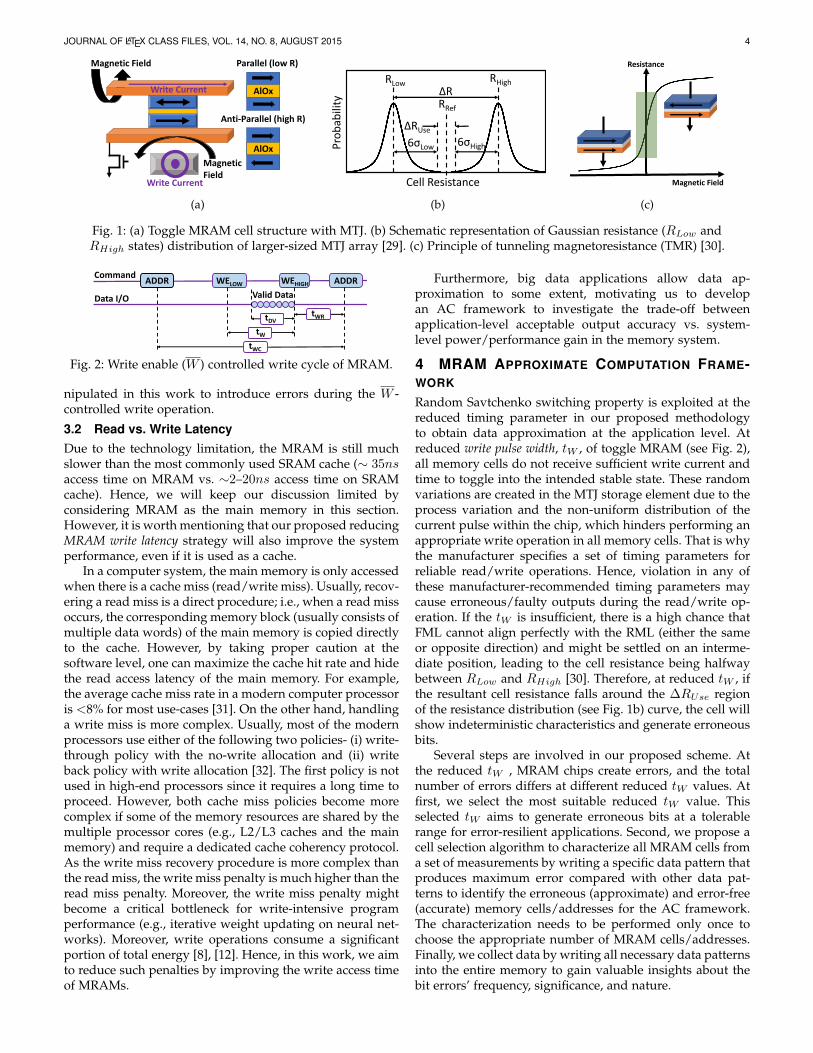
The core element of toggle MRAM is the magnetic tunneljunction (MTJ) that uses the Savtchenko switching [29]property to store both data states (high and low). The 1T-1MTJ MRAM bit cell comprises two ferromagnetic layersseparated by a thin dielectric tunnel oxide (AlOx or MgO)layer (Fig. 1a). One layer’s magnetic orientation is per-manently fixed, commonly referred to as the reference (orfixed) magnetic layer (RML). In contrast, the other layer’smagnetization can freely be oriented depending on themagnetic field, known as the free magnetic layer (FML). Thesubstantially higher magnetic anisotropy of RML comparedto FML ascertains the stable magnetization direction of FMLduring memory read/write operation. The resistance statesdetermine the bit that will be stored in the memory array.
When both the FML and RML are aligned in the samedirection, the MTJ produces low electrical resistance. Onthe other hand, when their magnetic field orientation isopposite, the resistance becomes extremely large; hence,almost no current or weak current flows through the barrierlayer. Therefore, the MTJ exhibits high electrical resistance.
Writing a bit in the magnetic field-driven toggle MRAMarray requires passing a high write current (Iw) for changingFML’s magnetic orientation [29]. The applied Iw to the writelines, placed on top and bottom of the MTJ devices (see Fig.1a), creates an auxiliary magnetic field that changes the FMLdirection in the required position. Contrastingly, the RML’sdirection is strongly coupled with an anti-ferromagnet [29].During the write operation, the memory circuit performsa pre-read operation to determine the state of the targetbit and execute a toggle pulse (if required) to change thestate of the bit if the desired state is not the same as thetargeted state. Consequently, it reduces the overall powerconsumption and improves power efficiency. However, thisincreases the total write cycle time (including an additionalread operation).
A small bias voltage (far below the device’s breakdownvoltage) is applied across the MRAM cell during the readcycle. Depending on parallel (RLow) or anti-parallel (RHigh)magnetic orientation, a current sensing circuitry that isattached with the MRAM cell experiences different amountsof current and latches the appropriate logic (“0” or “1”)compared with the reference resistance (RRef ) shown in Fig.1b. Note that the width of resistance distribution varies fromcell to cell because of manufacturing process variations.Besides, the quality, size, and level of in-homogeneity ofthe MTJ tunnel barrier significantly impact larger relativebit-to-bit resistance variation [29].
However, from Fig. 1c, we observe that the change inresistance due to the change in the induced magnetic fieldis steep in a certain region (the green region on Fig. 1c). Inthis region, a slight change in the induced magnetic fieldmay cause a drastic change in resistance states and alterthe decision of the read circuitry. Therefore, manufacturersdefine timing parameters for all commercial memory chipsfor reliable write/read operation against a wide range ofoperating conditions. For toggle MRAM, the write oper-ation is governed by three different control signals: writeenable (W ), chip enable (E), and upper/lower byte enable(UB/LB) signals [15]. A simplified version of the writeenable (W ) controlled write operation of the MRAM chipis shown in Fig. 2.
Here,tWC = write cycle time, i.e., the time period to complete
full write operation in a particular address.tW = write pulse width, i.e., the time period for which the
W pin is kept activated.tWR = write recovery time, i.e., the time to complete the
write operation after the W pin is deactivated.tDV = valid data to end of write, i.e., the time for which the
valid data need to be available in the data I/O before the Wpin is deactivated.
Reducing any of these timing parameters can improvethe speed and reduce power consumption but may leadto faulty operation. The write timing parameter tW is ma-
JOURNAL OF LATEX CLASS FILES, VOL. 14, NO. 8, AUGUST 2015 4
Write Current
Write Current
Magnetic Field
Magnetic Field
AlOx
Parallel (low R)
AlOx
Anti-Parallel (high R)
(a)
Cell Resistance
Pro
bab
ility
RHighRLow
RRef
ΔRUse
ΔR
6σLow 6σHigh
(b)
Magnetic Field
Resistance
(c)
Fig. 1: (a) Toggle MRAM cell structure with MTJ. (b) Schematic representation of Gaussian resistance (RLow andRHigh states) distribution of larger-sized MTJ array [29]. (c) Principle of tunneling magnetoresistance (TMR) [30].
ADDR WELOW ADDRWEHIGH
tWC
tW
tWR
Data I/O
Command
Valid Data
tDV
Fig. 2: Write enable (W ) controlled write cycle of MRAM.
nipulated in this work to introduce errors during the W -controlled write operation.
3.2 Read vs. Write LatencyDue to the technology limitation, the MRAM is still muchslower than the most commonly used SRAM cache (∼ 35nsaccess time on MRAM vs. ∼2–20ns access time on SRAMcache). Hence, we will keep our discussion limited byconsidering MRAM as the main memory in this section.However, it is worth mentioning that our proposed reducingMRAM write latency strategy will also improve the systemperformance, even if it is used as a cache.
In a computer system, the main memory is only accessedwhen there is a cache miss (read/write miss). Usually, recov-ering a read miss is a direct procedure; i.e., when a read missoccurs, the corresponding memory block (usually consists ofmultiple data words) of the main memory is copied directlyto the cache. However, by taking proper caution at thesoftware level, one can maximize the cache hit rate and hidethe read access latency of the main memory. For example,the average cache miss rate in a modern computer processoris <8% for most use-cases [31]. On the other hand, handlinga write miss is more complex. Usually, most of the modernprocessors use either of the following two policies- (i) write-through policy with the no-write allocation and (ii) writeback policy with write allocation [32]. The first policy is notused in high-end processors since it requires a long time toproceed. However, both cache miss policies become morecomplex if some of the memory resources are shared by themultiple processor cores (e.g., L2/L3 caches and the mainmemory) and require a dedicated cache coherency protocol.As the write miss recovery procedure is more complex thanthe read miss, the write miss penalty is much higher than theread miss penalty. Moreover, the write miss penalty mightbecome a critical bottleneck for write-intensive programperformance (e.g., iterative weight updating on neural net-works). Moreover, write operations consume a significantportion of total energy [8], [12]. Hence, in this work, we aimto reduce such penalties by improving the write access timeof MRAMs.
Furthermore, big data applications allow data ap-proximation to some extent, motivating us to developan AC framework to investigate the trade-off betweenapplication-level acceptable output accuracy vs. system-level power/performance gain in the memory system.
4 MRAM APPROXIMATE COMPUTATION FRAME-WORK
Random Savtchenko switching property is exploited at thereduced timing parameter in our proposed methodologyto obtain data approximation at the application level. Atreduced write pulse width, tW , of toggle MRAM (see Fig. 2),all memory cells do not receive sufficient write current andtime to toggle into the intended stable state. These randomvariations are created in the MTJ storage element due to theprocess variation and the non-uniform distribution of thecurrent pulse within the chip, which hinders performing anappropriate write operation in all memory cells. That is whythe manufacturer specifies a set of timing parameters forreliable read/write operations. Hence, violation in any ofthese manufacturer-recommended timing parameters maycause erroneous/faulty outputs during the read/write op-eration. If the tW is insufficient, there is a high chance thatFML cannot align perfectly with the RML (either the sameor opposite direction) and might be settled on an interme-diate position, leading to the cell resistance being halfwaybetween RLow and RHigh [30]. Therefore, at reduced tW , ifthe resultant cell resistance falls around the ∆RUse regionof the resistance distribution (see Fig. 1b) curve, the cell willshow indeterministic characteristics and generate erroneousbits.
Several steps are involved in our proposed scheme. Atthe reduced tW , MRAM chips create errors, and the totalnumber of errors differs at different reduced tW values. Atfirst, we select the most suitable reduced tW value. Thisselected tW aims to generate erroneous bits at a tolerablerange for error-resilient applications. Second, we propose acell selection algorithm to characterize all MRAM cells froma set of measurements by writing a specific data pattern thatproduces maximum error compared with other data pat-terns to identify the erroneous (approximate) and error-free(accurate) memory cells/addresses for the AC framework.The characterization needs to be performed only once tochoose the appropriate number of MRAM cells/addresses.Finally, we collect data by writing all necessary data patternsinto the entire memory to gain valuable insights about thebit errors’ frequency, significance, and nature.
JOURNAL OF LATEX CLASS FILES, VOL. 14, NO. 8, AUGUST 2015 5
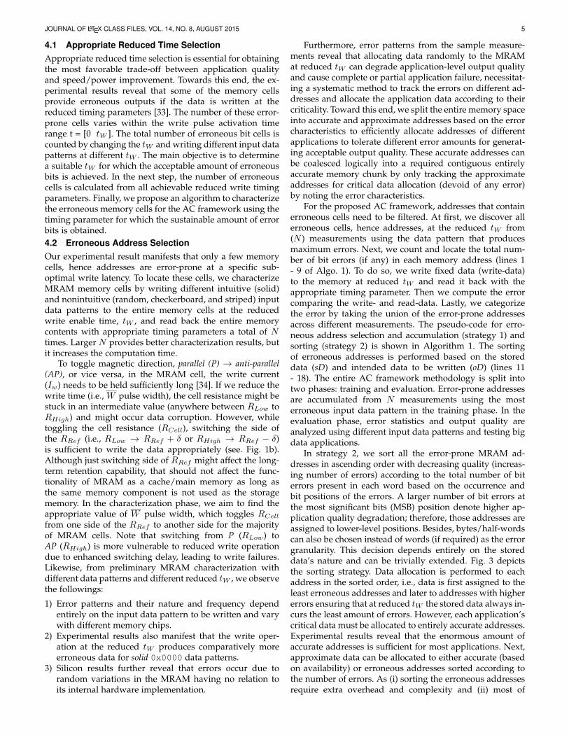
4.1 Appropriate Reduced Time SelectionAppropriate reduced time selection is essential for obtainingthe most favorable trade-off between application qualityand speed/power improvement. Towards this end, the ex-perimental results reveal that some of the memory cellsprovide erroneous outputs if the data is written at thereduced timing parameters [33]. The number of these error-prone cells varies within the write pulse activation timerange t = [0 tW ]. The total number of erroneous bit cells iscounted by changing the tW and writing different input datapatterns at different tW . The main objective is to determinea suitable tW for which the acceptable amount of erroneousbits is achieved. In the next step, the number of erroneouscells is calculated from all achievable reduced write timingparameters. Finally, we propose an algorithm to characterizethe erroneous memory cells for the AC framework using thetiming parameter for which the sustainable amount of errorbits is obtained.4.2 Erroneous Address SelectionOur experimental result manifests that only a few memorycells, hence addresses are error-prone at a specific sub-optimal write latency. To locate these cells, we characterizeMRAM memory cells by writing different intuitive (solid)and nonintuitive (random, checkerboard, and striped) inputdata patterns to the entire memory cells at the reducedwrite enable time, tW , and read back the entire memorycontents with appropriate timing parameters a total of Ntimes. Larger N provides better characterization results, butit increases the computation time.
To toggle magnetic direction, parallel (P) → anti-parallel(AP), or vice versa, in the MRAM cell, the write current(Iw) needs to be held sufficiently long [34]. If we reduce thewrite time (i.e., W pulse width), the cell resistance might bestuck in an intermediate value (anywhere between RLow toRHigh) and might occur data corruption. However, whiletoggling the cell resistance (RCell), switching the side ofthe RRef (i.e., RLow → RRef + δ or RHigh → RRef − δ)is sufficient to write the data appropriately (see. Fig. 1b).Although just switching side of RRef might affect the long-term retention capability, that should not affect the func-tionality of MRAM as a cache/main memory as long asthe same memory component is not used as the storagememory. In the characterization phase, we aim to find theappropriate value of W pulse width, which toggles RCellfrom one side of the RRef to another side for the majorityof MRAM cells. Note that switching from P (RLow) toAP (RHigh) is more vulnerable to reduced write operationdue to enhanced switching delay, leading to write failures.Likewise, from preliminary MRAM characterization withdifferent data patterns and different reduced tW , we observethe followings:
1) Error patterns and their nature and frequency dependentirely on the input data pattern to be written and varywith different memory chips.
2) Experimental results also manifest that the write oper-ation at the reduced tW produces comparatively moreerroneous data for solid 0x0000 data patterns.
3) Silicon results further reveal that errors occur due torandom variations in the MRAM having no relation toits internal hardware implementation.
Furthermore, error patterns from the sample measure-ments reveal that allocating data randomly to the MRAMat reduced tW can degrade application-level output qualityand cause complete or partial application failure, necessitat-ing a systematic method to track the errors on different ad-dresses and allocate the application data according to theircriticality. Toward this end, we split the entire memory spaceinto accurate and approximate addresses based on the errorcharacteristics to efficiently allocate addresses of differentapplications to tolerate different error amounts for generat-ing acceptable output quality. These accurate addresses canbe coalesced logically into a required contiguous entirelyaccurate memory chunk by only tracking the approximateaddresses for critical data allocation (devoid of any error)by noting the error characteristics.
For the proposed AC framework, addresses that containerroneous cells need to be filtered. At first, we discover allerroneous cells, hence addresses, at the reduced tW from(N ) measurements using the data pattern that producesmaximum errors. Next, we count and locate the total num-ber of bit errors (if any) in each memory address (lines 1- 9 of Algo. 1). To do so, we write fixed data (write-data)to the memory at reduced tW and read it back with theappropriate timing parameter. Then we compute the errorcomparing the write- and read-data. Lastly, we categorizethe error by taking the union of the error-prone addressesacross different measurements. The pseudo-code for erro-neous address selection and accumulation (strategy 1) andsorting (strategy 2) is shown in Algorithm 1. The sortingof erroneous addresses is performed based on the storeddata (sD) and intended data to be written (oD) (lines 11- 18). The entire AC framework methodology is split intotwo phases: training and evaluation. Error-prone addressesare accumulated from N measurements using the mosterroneous input data pattern in the training phase. In theevaluation phase, error statistics and output quality areanalyzed using different input data patterns and testing bigdata applications.
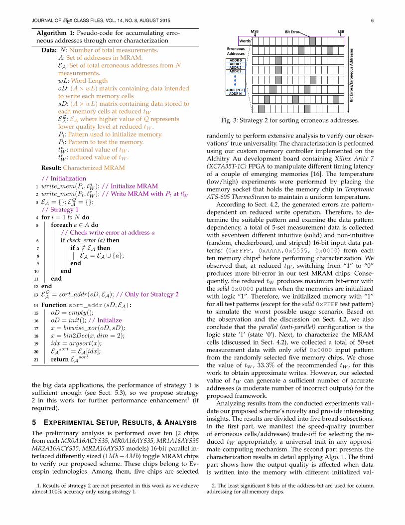
In strategy 2, we sort all the error-prone MRAM ad-dresses in ascending order with decreasing quality (increas-ing number of errors) according to the total number of biterrors present in each word based on the occurrence andbit positions of the errors. A larger number of bit errors atthe most significant bits (MSB) position denote higher ap-plication quality degradation; therefore, those addresses areassigned to lower-level positions. Besides, bytes/half-wordscan also be chosen instead of words (if required) as the errorgranularity. This decision depends entirely on the storeddata’s nature and can be trivially extended. Fig. 3 depictsthe sorting strategy. Data allocation is performed to eachaddress in the sorted order, i.e., data is first assigned to theleast erroneous addresses and later to addresses with highererrors ensuring that at reduced tW the stored data always in-curs the least amount of errors. However, each application’scritical data must be allocated to entirely accurate addresses.Experimental results reveal that the enormous amount ofaccurate addresses is sufficient for most applications. Next,approximate data can be allocated to either accurate (basedon availability) or erroneous addresses sorted according tothe number of errors. As (i) sorting the erroneous addressesrequire extra overhead and complexity and (ii) most of
JOURNAL OF LATEX CLASS FILES, VOL. 14, NO. 8, AUGUST 2015 6
Algorithm 1: Pseudo-code for accumulating erro-neous addresses through error characterization
Data: N : Number of total measurements.A: Set of addresses in MRAM.EA: Set of total erroneous addresses from Nmeasurements.wL: Word LengthoD: (A×wL) matrix containing data intendedto write each memory cellssD: (A×wL) matrix containing data stored toeach memory cells at reduced tWEQA : EA where higher value of Q representslower quality level at reduced tW .Pi: Pattern used to initialize memory.Pt: Pattern to test the memory.tnW : nominal value of tW .trW : reduced value of tW .
Result: Characterized MRAM
// Initialization1 write mem(Pi, t
nW ); // Initialize MRAM
2 write mem(Pt, trW ); // Write MRAM with Pt at trW
3 EA = {}; EQA = {};// Strategy 1
4 for i = 1 to N do5 foreach a ∈ A do
// Check write error at address a6 if check error (a) then7 if a /∈ EA then8 EA = EA ∪ {a};9 end
10 end11 end12 end13 EQA = sort addr(sD, EA); // Only for Strategy 2
14 Function sort_addr(sD, EA):15 oD = empty();16 oD = init(); // Initialize17 x = bitwise xor(oD, sD);18 x = bin2Dec(x, dim = 2);19 idx = argsort(x);20 EAsort = EA[idx];21 return EAsort
the big data applications, the performance of strategy 1 issufficient enough (see Sect. 5.3), so we propose strategy2 in this work for further performance enhancement1 (ifrequired).
5 EXPERIMENTAL SETUP, RESULTS, & ANALYSIS
The preliminary analysis is performed over ten (2 chipsfrom each MR0A16ACYS35, MR0A16AYS35, MR1A16AYS35MR2A16ACYS35, MR2A16AYS35 models) 16-bit parallel in-terfaced differently sized (1Mb− 4Mb) toggle MRAM chipsto verify our proposed scheme. These chips belong to Ev-erspin technologies. Among them, five chips are selected
1. Results of strategy 2 are not presented in this work as we achievealmost 100% accuracy only using strategy 1.
ADDR 0ADDR 1ADDR 2ADDR 3
ADDR (N -1)ADDR N
LSBMSB
Erroneous Addresses
Words
Bit Error
Bit
Err
ors
/Err
on
eou
s A
dd
ress
es
Fig. 3: Strategy 2 for sorting erroneous addresses.
randomly to perform extensive analysis to verify our obser-vations’ true universality. The characterization is performedusing our custom memory controller implemented on theAlchitry Au development board containing Xilinx Artix 7(XC7A35T-1C) FPGA to manipulate different timing latencyof a couple of emerging memories [16]. The temperature(low/high) experiments were performed by placing thememory socket that holds the memory chip in TemptronicATS-605 ThermoStream to maintain a uniform temperature.
According to Sect. 4.2, the generated errors are pattern-dependent on reduced write operation. Therefore, to de-termine the suitable pattern and examine the data patterndependency, a total of 5-set measurement data is collectedwith seventeen different intuitive (solid) and non-intuitive(random, checkerboard, and striped) 16-bit input data pat-terns: (0xFFFF, 0xAAAA,0x5555, 0x0000) from eachten memory chips2 before performing characterization. Weobserved that, at reduced tW , switching from “1” to “0”produces more bit-error in our test MRAM chips. Conse-quently, the reduced tW produces maximum bit-error withthe solid 0x0000 pattern when the memories are initializedwith logic “1”. Therefore, we initialized memory with “1”for all test patterns (except for the solid 0xFFFF test pattern)to simulate the worst possible usage scenario. Based onthe observation and the discussion on Sect. 4.2, we alsoconclude that the parallel (anti-parallel) configuration is thelogic state ’1’ (state ’0’). Next, to characterize the MRAMcells (discussed in Sect. 4.2), we collected a total of 50-setmeasurement data with only solid 0x0000 input patternfrom the randomly selected five memory chips. We chosethe value of tW , 33.3% of the recommended tW , for thiswork to obtain approximate writes. However, our selectedvalue of tW can generate a sufficient number of accurateaddresses (a moderate number of incorrect outputs) for theproposed framework.
Analyzing results from the conducted experiments vali-date our proposed scheme’s novelty and provide interestinginsights. The results are divided into five broad subsections.In the first part, we manifest the speed-quality (numberof erroneous cells/addresses) trade-off for selecting the re-duced tW appropriately, a universal trait in any approxi-mate computing mechanism. The second part presents thecharacterization results in detail applying Algo. 1. The thirdpart shows how the output quality is affected when datais written into the memory with different initialized val-
2. The least significant 8 bits of the address-bit are used for columnaddressing for all memory chips.
JOURNAL OF LATEX CLASS FILES, VOL. 14, NO. 8, AUGUST 2015 7
ues and with or without applying the proposed addressselection strategy (strategy 1 of Algo. 1). We also showthat our approach results in comparably higher performanceimprovement than many popular (non) volatile memory-based prior works [8], [9], [10], [12]. Moreover, an efficientimplementation of a memory controller can further improvethe overall performance of our proposed framework. Notethat all results are presented in the Sects. 5.2 and 5.3 areobtained at room temperature (26◦C). The fourth part de-scribes the approximate MRAM results subject to operatingconditions and memory chip variations. Finally, the fifthpart elucidates our proposed technique’s power analysisresults.
5.1 Selection of tWAn extensive analysis is performed to determine the errorprofile, such as frequency, location of the bit errors, compar-ing the behavior of the faulty/erroneous outputs at differentreduced tW values using solid 0x0000 data pattern. Wereduce the tW value from 15ns (manufacturer’s recom-mended) to 10ns, 5ns, and 2.5ns, respectively (Fig. 4). Notethat our experimental setup’s timing resolution is limited to2.5ns. At tW = 2.5ns, the total failed bit counts fall within∼20% – ∼95%, which spans over ∼23% – ∼95% addresses.Our analysis shows that higher bit errors can be usedfor random number generation and physical unclonablefunction [33] but is not suitable for approximate computing.However, at tW = 5ns and 10ns, the obtained total failedbits are almost negligible (<5% and <1%, respectively) forall ten chips (considering a single measurement). Hence,we choose tW = 5ns (considering the number of failedbit counts) to characterize erroneous cells to improve writespeed (∼29% overall improvement) and power savings (seeSect. 5.5).
2.5 5.0 7.5 10.0 12.5 15.00
25
50
75
100
2.5 5.0 7.5 10.0 12.5 15.0
C1 C2 C3 C4 C5
Erro
r (%
)
tw (ns)
Bit error Address error
Fig. 4: tW vs. errors for five randomly chosen chips. Theleft and right figures present % of erroneous bits and % ofaddresses which consist those erroneous bits, respectively.
5.2 Characterization of Error-Prone CellsThe cell characterization of MRAM is performed accordingto Sect. 4.2 with N = 50 temporal measurements. Solid0x0000 is used as the write data pattern. Moreover, theentire memory is reset with the solid 0xFFFF data patternbefore every measurement to erase previously written datatraces. In Table 1, the first two rows show the statistics oferroneous MRAM addresses and bits after performing theproposed cell characterization algorithm (strategy 1 of Algo.1). Here, EA is the percentage of total erroneous addresses,and EB is the percentage of total erroneous bits accumulatedfrom 50 temporal measurements (obtained through charac-terization). The results manifest that the total number oferroneous bits obtained at reduced tW (5ns) varies from
chip to chip. We also observe that only a few addresseshold these erroneous bits. The rest of the rows representerroneous addresses and bits from different data patternsand to which extent they belong to EA and EB. Here,MA isthe percentage of total erroneous addresses, andMB is thepercentage of total erroneous bits from a specific test pattern(from a single measurement), and CA is the percentage ofMA belonging to EA. Similarly, CB is the percentage ofMBbelonging to EB.
Table 1 represents that, after performing characterizationusing N = 50 temporal measurements with solid 0x0000data pattern, the cumulative amount of erroneous addressesis 22.41% (EA), and bits is 10.49% (EB) for chip 1 (C1).During the testing phase, the number of erroneous ad-dresses observed using solid 0x0000 data pattern is only2.52% (MA), and bits is only 0.83% (MB). Now, amongthese 2.52% erroneous addresses, 96.92% (CA) of addressesbelong to the 22.41% (EA), and 85.48% (CB) of bits belongto the 10.49% (EB).
In summary, the cumulative maximum amount of erro-neous addresses is 26.41% (EA), whereas the minimum isonly 5.33% (1st row of characterization segment in Table1) for different memory chips at tW = 5ns. Similarly, inTable 1, the cumulative maximum amount of erroneousbit is 22.06% (EB), whereas the minimum is only 3.89%(2nd row of characterization segment). This indicates that∼75% of the addresses (∼78% of bits) are entirely accuratein the worst case scenario, resulting in negligible or noloss in output quality. As the percentage of error-proneaddresses is fairly small (∼25%) regardless of memory size,storage overhead is minimal for storing these few memoryaddresses’ information.
For pattern 0xAAAA or 0x5555, we do not observe anyerror for any data pattern. Based on the internal architectureof MRAM, there might be different reasons behind notgetting any error. For example, if all of the I/O buffers aredriven by the same power rail, the inrush current caused bythe I/O buffers should be lower for these specific data pat-terns as only 8 out of 16 bits experience the switching [35].Hence, the overall timing characteristics might be improved[35]. Moreover, the maximum obtained erroneous address(MA) is 6.04%, whereas the minimum is only 0.16% for anygiven pattern considering a single test measurement. Simi-larly, the maximum obtained erroneous bit (MB) is 3.30%,whereas the minimum is only 0.08%. Besides, our proposedcharacterization technique covers most erroneous addresses(CA) and bits (CB) for all data patterns. We observed that thelowest covered erroneous address (CA) is 1.74% and bit (CB)is 2.76% for solid 0xFFFF data pattern. However, a closerobservation reveals that solid 0xFFFF data pattern producesonly 0.26% erroneous addresses and 0.23% erroneous bits,which is negligible (< 0.5%). This insignificant number oferrors can be overlooked for any big data application.
Note that taking the union of the errors resulting fromeach data pattern (0xFFFF, 0xAAAA,0x5555, 0x0000)can further improve the fault coverage for the worst case.However, only a marginal improvement is observed for
1. C1: MR0A16AYS35, C2: MR1A16AYS35, C3&C4: MR2A16ACYS35,C5: MR2A16AYS35. C1,C2&C5: Commercial Grade (Temp. range[0◦C 70◦C]); C3&C4: Industrial Grade (Temp. range [−40◦C 85◦C]).
2. Solid/ Striped/ Checkerboard.
JOURNAL OF LATEX CLASS FILES, VOL. 14, NO. 8, AUGUST 2015 8
TABLE 1: Error Characteristics.
Sample Chip3 (%) C1 C2 C3 C4 C5
Characterization EA 22.41 26.41 10.34 8.36 5.33EB 10.49 22.06 7.60 5.15 3.89
Solid
FFFF
MA 0.26 0.26 0 0 0MB 0.11 0.23 0 0 0CA 1.74 60.81 —- —- —-CB 2.76 54.39 —- —- —-
0000
MA 2.52 6.04 1.83 2.04 1.29MB 0.83 3.30 1.25 1.36 0.86CA 96.92 99.28 95.26 86.23 94.34CB 85.48 98.36 94.37 80.73 91.5
RowStriped
FFFF
MA 1.99 3.52 0.72 0.82 0.62MB 0.67 2.13 0.53 0.56 0.47CA 97.78 99.55 95.2 92.87 95.78CB 90.9 98.34 94.42 91.43 94.11
0000
MA 0.75 2.63 0.94 1.09 0.67MB 0.18 1.25 0.61 0.68 0.40CA 97.77 99.45 96.8 84.29 94.03CB 83.07 98.55 96.02 76.87 90.46
ColumnStriped
FFFF
MA 1.68 0 1.06 1.27 0.89MB 0.67 0 0.71 0.79 0.60CA 87.4 — 93.13 90.23 89.82CB 74.8 — 92.75 89.73 88.73
0000
MA 1.37 1.18 0.32 0.37 0.22MB 0.54 0.94 0.19 0.20 0.12CA 46.99 90.73 51.74 32.89 34.93CB 47.51 93.23 51.25 29.09 35.42
Checker-board
FFFF
MA 1.59 3.05 0.71 0.84 0.61MB 0.60 1.77 0.51 0.53 0.41CA 76.3 96.02 83.44 74.97 79.47CB 68.07 93.81 83.96 76.62 80.64
0000
MA 1.25 2.96 0.64 0.75 0.49MB 0.59 1.55 0.40 0.42 0.29CA 62.61 96.02 85.71 83.54 81.54CB 60.43 93.62 83.97 82.49 79.89
AnyPattern4
5555 /AAAA
MA 0 0 0 0 0MB 0 0 0 0 0CA —- —- —- — —CB —- —- —- — —
Random
MA 0.27 0.28 0.22 0.19 0.16MB 0.13 0.13 0.11 0.42 0.08CA 34.83 68.94 13.97 10.18 10.12CB 20.99 62.47 11.5 7.55 8.02
∗NB. —- not performed as no error occurred at reduced tW for corr-esponding data patterns.
the chips used for experiments using different data pat-terns over the solid 0x0000 data pattern. Besides, Table1 shows that a vast portion of the erroneous addresses(MA) generated from different data patterns belongs tothose erroneous addresses (EA) obtained through the ad-dress selection strategy from error characterization usingsolid 0x0000 data pattern (described in strategy 1 of Algo.1). Furthermore, it is essential to note that the acquirederroneous addresses heavily depend on the training dataand frequency characteristics. Hence, it becomes imperativeto select the training data and frequency judiciously.
5.3 EvaluationWe evaluate our proposed AC framework with two dif-ferent end-user applications- (i) JPEG image compressionand (ii) optical character recognition (OCR) using the K-nearest neighbors (KNN) algorithm [12]. Fig. 5 presentsthe evaluation scheme for our proposed AC framework.We use this scheme to emulate MRAM as the main mem-ory for both applications. Conventionally, memory alloca-tion/deallocation (resource management) is accomplishedat the application level with the assistance of the operatingsystem (application-level memory management) [36]. Onthe other hand, a memory management unit (MMU) is a
separate entity responsible for translating virtual addressesinto physical addresses. Although traditionally, MMU is ahardware unit, software implementation of memory man-agement is also feasible without requiring virtual addresses[37]. To simplify our experimental setup, we fuse the re-source manager and the MMU in a single python API(similar to [37]). This python API also interfaces our custommemory controller, built on an FPGA board.
ApplicationApplication-
level Memory Management
Memory Controller
MRAM
Python APIFPGA
Implementation
Memory Management Unit (MMU)
Fig. 5: Evaluation scheme for proposed AC.For JPEG application, we use the most common and pop-
ular metrics, signal-to-noise ratio (SNR), mean squared error(MSE), and peak signal-to-noise ratio (PSNR), between theapproximated image and the unapproximated image usedin the JPEG compression to quantify the acceptability of theapplication output quality. The SNR, MSE, and PSNR arecalculated using the following equations (Eqs. 1 to 3). Here,f̂(i, j) and f(i, j) are the compressed JPEG image data withand without applying our AC framework, respectively. Notethat the size of the images is M ×N , where M = N = 90.Besides, MAXI is the maximum possible pixel value ofthe image. Here, the pixels are represented using 8 bits persample; hence, MAXI = 255.
SNR =
∑Mi=1
∑Nj=1 f̂(i, j)2∑M
i=1
∑Nj=1[f̂(i, j)− f(i, j)]2
(1)
MSE =1
MN
M∑i=1
N∑j=1
[f̂(i, j)− f(i, j)]2 (2)
PSNR = 10. log10(MAX2
I
MSE) (3)
The value of SNR, MSE, and PSNR measures the im-age’s quality of JPEG compression output, evaluating theproposed scheme’s effectiveness. A minimum SNR value isrequired for such applications for the approximated imagewhere the human brain and eyes can differentiate betweenthe approximated and unapproximated image. A lower SNRvalue is considered as unacceptable output quality and viceversa. Similarly, a higher MSE value is considered as un-acceptable output quality. The SNR, MSE, and PSNR mea-surements reveal the degree to which an application couldproduce satisfactory and reasonable output at reduced tWfor approximate applications and determine the achievablelimits of the performance and power improvements forMRAM technology. Fig. 6 shows the unapproximate andapproximate output image quality with and without apply-ing the proposed addresses selection technique (strategy 1of Algo. 1), considering two different initialization states.The SNR of the image is infinite (MSE of the image is zero)means it does not have any errors relative to the unapprox-imated image output (Table 3). Observing the images andthe related SNR and MSE reveals the appropriateness of theproposed technique through application quality.
We have presented our results with and without theaddress selection technique in this work. In the “without
JOURNAL OF LATEX CLASS FILES, VOL. 14, NO. 8, AUGUST 2015 9
Original image Without address selection With address selection Without address selection
(E1) (E2) (E3) (E4)
(M1) (M2) (M3) (M4)
Initialized with 1’s Initialized with 0’s
(a)
Original image Without address selection With address selection Without address selection
(E1) (E2) (E3) (E4)
(M1) (M2) (M3) (M4)
Initialized with 1’s Initialized with 0’s
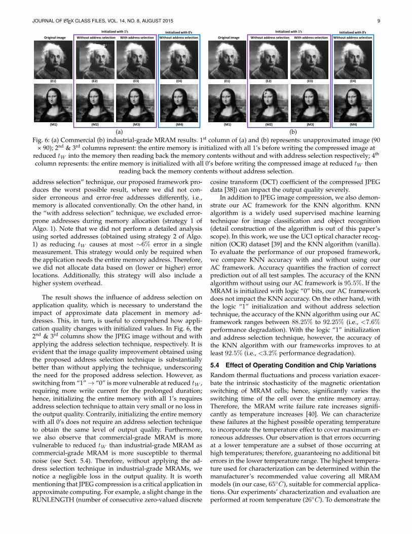
(b)Fig. 6: (a) Commercial (b) industrial-grade MRAM results. 1st column of (a) and (b) represents: unapproximated image (90
× 90); 2nd & 3rd columns represent: the entire memory is initialized with all 1’s before writing the compressed image atreduced tW into the memory then reading back the memory contents without and with address selection respectively; 4th
column represents: the entire memory is initialized with all 0’s before writing the compressed image at reduced tW thenreading back the memory contents without address selection.
address selection” technique, our proposed framework pro-duces the worst possible result, where we did not con-sider erroneous and error-free addresses differently, i.e.,memory is allocated conventionally. On the other hand, inthe “with address selection” technique, we excluded error-prone addresses during memory allocation (strategy 1 ofAlgo. 1). Note that we did not perform a detailed analysisusing sorted addresses (obtained using strategy 2 of Algo.1) as reducing tW causes at most ∼6% error in a singlemeasurement. This strategy would only be required whenthe application needs the entire memory address. Therefore,we did not allocate data based on (lower or higher) errorlocations. Additionally, this strategy will also include ahigher system overhead.
The result shows the influence of address selection onapplication quality, which is necessary to understand theimpact of approximate data placement in memory ad-dresses. This, in turn, is useful to comprehend how appli-cation quality changes with initialized values. In Fig. 6, the2nd & 3rd columns show the JPEG image without and withapplying the address selection technique, respectively. It isevident that the image quality improvement obtained usingthe proposed address selection technique is substantiallybetter than without applying the technique, underscoringthe need for the proposed address selection. However, asswitching from “1”→ “0” is more vulnerable at reduced tW ,requiring more write current for the prolonged duration;hence, initializing the entire memory with all 1’s requiresaddress selection technique to attain very small or no loss inthe output quality. Contrarily, initializing the entire memorywith all 0’s does not require an address selection techniqueto obtain the same level of output quality. Furthermore,we also observe that commercial-grade MRAM is morevulnerable to reduced tW than industrial-grade MRAM ascommercial-grade MRAM is more susceptible to thermalnoise (see Sect. 5.4). Therefore, without applying the ad-dress selection technique in industrial-grade MRAMs, wenotice a negligible loss in the output quality. It is worthmentioning that JPEG compression is a critical application inapproximate computing. For example, a slight change in theRUNLENGTH (number of consecutive zero-valued discrete
cosine transform (DCT) coefficient of the compressed JPEGdata [38]) can impact the output quality severely.
In addition to JPEG image compression, we also demon-strate our AC framework for the KNN algorithm. KNNalgorithm is a widely used supervised machine learningtechnique for image classification and object recognition(detail construction of the algorithm is out of this paper’sscope). In this work, we use the UCI optical character recog-nition (OCR) dataset [39] and the KNN algorithm (vanilla).To evaluate the performance of our proposed framework,we compare KNN accuracy with and without using ourAC framework. Accuracy quantifies the fraction of correctprediction out of all test samples. The accuracy of the KNNalgorithm without using our AC framework is 95.5%. If theMRAM is initialized with logic “0” bits, our AC frameworkdoes not impact the KNN accuracy. On the other hand, withthe logic “1” initialization and without address selectiontechnique, the accuracy of the KNN algorithm using our ACframework ranges between 88.25% to 92.25% (i.e., <7.6%performance degradation). With the logic “1” initializationand address selection technique, however, the accuracy ofthe KNN algorithm with our frameworks improves to atleast 92.5% (i.e., <3.2% performance degradation).
5.4 Effect of Operating Condition and Chip VariationsRandom thermal fluctuations and process variation exacer-bate the intrinsic stochasticity of the magnetic orientationswitching of MRAM cells; hence, significantly varies theswitching time of the cell over the entire memory array.Therefore, the MRAM write failure rate increases signifi-cantly as temperature increases [40]. We can characterizethese failures at the highest possible operating temperatureto incorporate the temperature effect to cover maximum er-roneous addresses. Our observation is that errors occurringat a lower temperature are a subset of those occurring athigh temperatures; therefore, guaranteeing no additional biterrors in the lower temperature range. The highest tempera-ture used for characterization can be determined within themanufacturer’s recommended value covering all MRAMmodels (in our case, 65◦C), suitable for commercial applica-tions. Our experiments’ characterization and evaluation areperformed at room temperature (26◦C). To demonstrate the
JOURNAL OF LATEX CLASS FILES, VOL. 14, NO. 8, AUGUST 2015 10
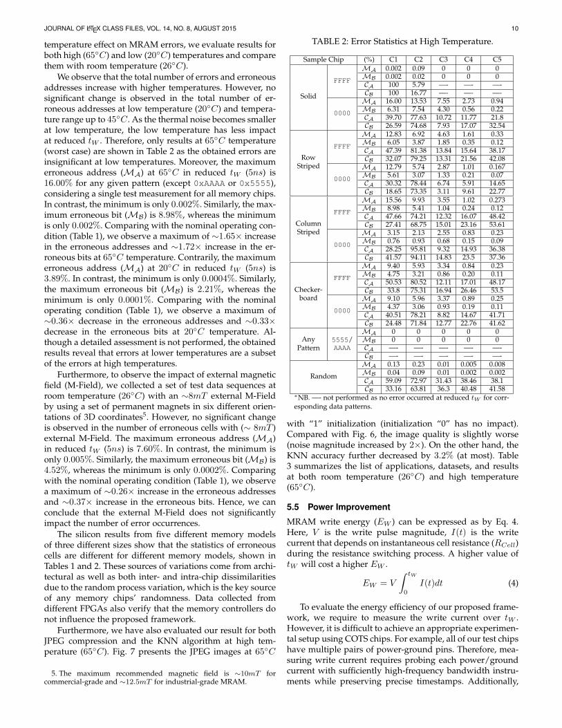
temperature effect on MRAM errors, we evaluate results forboth high (65◦C) and low (20◦C) temperatures and comparethem with room temperature (26◦C).
We observe that the total number of errors and erroneousaddresses increase with higher temperatures. However, nosignificant change is observed in the total number of er-roneous addresses at low temperature (20◦C) and tempera-ture range up to 45◦C . As the thermal noise becomes smallerat low temperature, the low temperature has less impactat reduced tW . Therefore, only results at 65◦C temperature(worst case) are shown in Table 2 as the obtained errors areinsignificant at low temperatures. Moreover, the maximumerroneous address (MA) at 65◦C in reduced tW (5ns) is16.00% for any given pattern (except 0xAAAA or 0x5555),considering a single test measurement for all memory chips.In contrast, the minimum is only 0.002%. Similarly, the max-imum erroneous bit (MB) is 8.98%, whereas the minimumis only 0.002%. Comparing with the nominal operating con-dition (Table 1), we observe a maximum of ∼1.65× increasein the erroneous addresses and ∼1.72× increase in the er-roneous bits at 65◦C temperature. Contrarily, the maximumerroneous address (MA) at 20◦C in reduced tW (5ns) is3.89%. In contrast, the minimum is only 0.0004%. Similarly,the maximum erroneous bit (MB) is 2.21%, whereas theminimum is only 0.0001%. Comparing with the nominaloperating condition (Table 1), we observe a maximum of∼0.36× decrease in the erroneous addresses and ∼0.33×decrease in the erroneous bits at 20◦C temperature. Al-though a detailed assessment is not performed, the obtainedresults reveal that errors at lower temperatures are a subsetof the errors at high temperatures.
Furthermore, to observe the impact of external magneticfield (M-Field), we collected a set of test data sequences atroom temperature (26◦C) with an ∼8mT external M-Fieldby using a set of permanent magnets in six different orien-tations of 3D coordinates5. However, no significant changeis observed in the number of erroneous cells with (∼ 8mT )external M-Field. The maximum erroneous address (MA)in reduced tW (5ns) is 7.60%. In contrast, the minimum isonly 0.005%. Similarly, the maximum erroneous bit (MB) is4.52%, whereas the minimum is only 0.0002%. Comparingwith the nominal operating condition (Table 1), we observea maximum of ∼0.26× increase in the erroneous addressesand ∼0.37× increase in the erroneous bits. Hence, we canconclude that the external M-Field does not significantlyimpact the number of error occurrences.
The silicon results from five different memory modelsof three different sizes show that the statistics of erroneouscells are different for different memory models, shown inTables 1 and 2. These sources of variations come from archi-tectural as well as both inter- and intra-chip dissimilaritiesdue to the random process variation, which is the key sourceof any memory chips’ randomness. Data collected fromdifferent FPGAs also verify that the memory controllers donot influence the proposed framework.
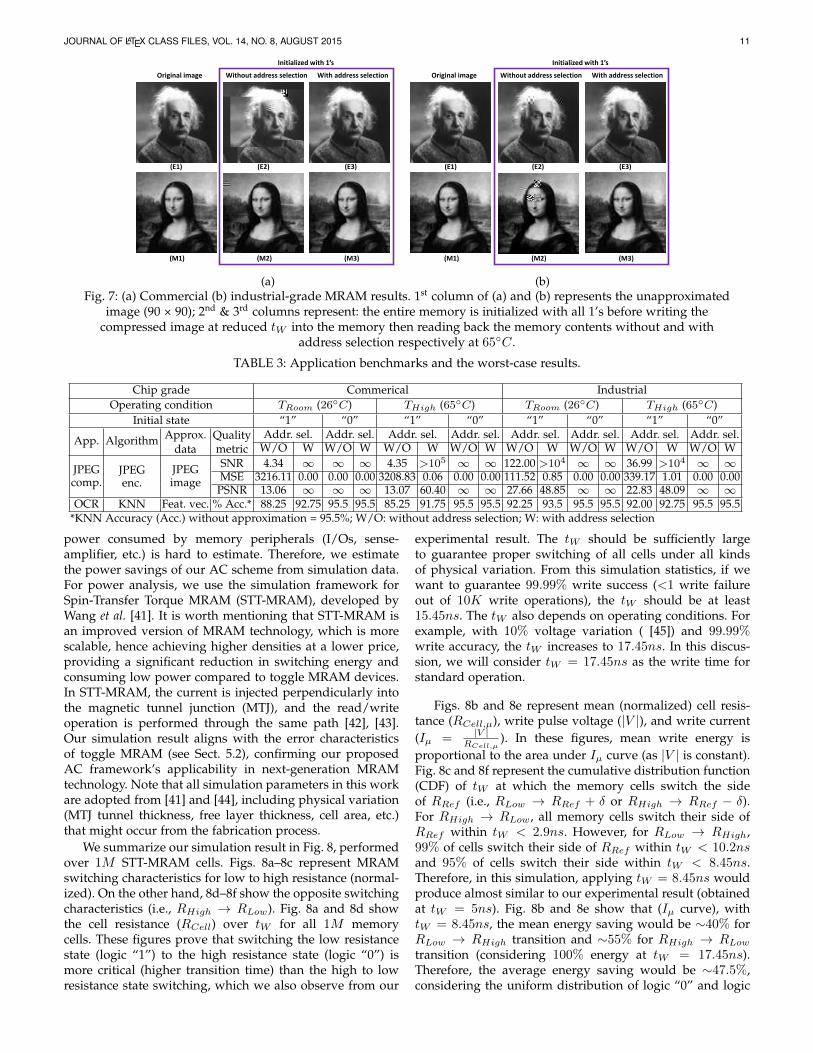
Furthermore, we have also evaluated our result for bothJPEG compression and the KNN algorithm at high tem-perature (65◦C). Fig. 7 presents the JPEG images at 65◦C
5. The maximum recommended magnetic field is ∼10mT forcommercial-grade and ∼12.5mT for industrial-grade MRAM.
TABLE 2: Error Statistics at High Temperature.
Sample Chip (%) C1 C2 C3 C4 C5
Solid
FFFF
MA 0.002 0.09 0 0 0MB 0.002 0.02 0 0 0CA 100 5.79 —- —- —-CB 100 16.77 —- —- —-
0000
MA 16.00 13.53 7.55 2.73 0.94MB 6.31 7.54 4.30 0.56 0.22CA 39.70 77.63 10.72 11.77 21.8CB 26.59 74.68 7.93 17.07 32.54
RowStriped
FFFF
MA 12.83 6.92 4.63 1.61 0.33MB 6.05 3.87 1.85 0.35 0.12CA 47.39 81.38 13.84 15.64 38.17CB 32.07 79.25 13.31 21.56 42.08
0000
MA 12.79 5.74 2.87 1.01 0.167MB 5.61 3.07 1.33 0.21 0.07CA 30.32 78.44 6.74 5.91 14.65CB 18.65 73.35 3.11 9.61 22.77
ColumnStriped
FFFF
MA 15.56 9.93 3.55 1.02 0.273MB 8.98 5.41 1.04 0.24 0.12CA 47.66 74.21 12.32 16.07 48.42CB 27.41 68.75 15.01 23.16 53.61
0000
MA 3.15 2.13 2.55 0.83 0.23MB 0.76 0.93 0.68 0.15 0.09CA 28.25 95.81 9.32 14.93 36.38CB 41.57 94.11 14.83 23.5 37.36
Checker-board
FFFF
MA 9.40 5.93 3.34 0.84 0.23MB 4.75 3.21 0.86 0.20 0.11CA 50.53 80.52 12.11 17.01 48.17CB 33.8 75.31 16.94 26.46 53.5
0000
MA 9.10 5.96 3.37 0.89 0.25MB 4.37 3.06 0.93 0.19 0.11CA 40.51 78.21 8.82 14.67 41.71CB 24.48 71.84 12.77 22.76 41.62
AnyPattern
5555/AAAA
MA 0 0 0 0 0MB 0 0 0 0 0CA —- —- —- —- —-CB —- —- —- —- —-
Random
MA 0.13 0.23 0.01 0.005 0.008MB 0.04 0.09 0.01 0.002 0.002CA 59.09 72.97 31.43 38.46 38.1CB 33.16 63.81 36.3 40.48 41.58
∗NB. —- not performed as no error occurred at reduced tW for corr-esponding data patterns.
with “1” initialization (initialization “0” has no impact).Compared with Fig. 6, the image quality is slightly worse(noise magnitude increased by 2×). On the other hand, theKNN accuracy further decreased by 3.2% (at most). Table3 summarizes the list of applications, datasets, and resultsat both room temperature (26◦C) and high temperature(65◦C).
5.5 Power Improvement
MRAM write energy (EW ) can be expressed as by Eq. 4.Here, V is the write pulse magnitude, I(t) is the writecurrent that depends on instantaneous cell resistance (RCell)during the resistance switching process. A higher value oftW will cost a higher EW .
EW = V
∫ tW
0
I(t)dt (4)
To evaluate the energy efficiency of our proposed frame-work, we require to measure the write current over tW .However, it is difficult to achieve an appropriate experimen-tal setup using COTS chips. For example, all of our test chipshave multiple pairs of power-ground pins. Therefore, mea-suring write current requires probing each power/groundcurrent with sufficiently high-frequency bandwidth instru-ments while preserving precise timestamps. Additionally,
JOURNAL OF LATEX CLASS FILES, VOL. 14, NO. 8, AUGUST 2015 11
Original image Without address selection With address selection
(E1) (E2) (E3)
(M1) (M2) (M3)
Initialized with 1’s
(a)
Original image Without address selection With address selection
(E1) (E2) (E3)
(M1) (M2) (M3)
Initialized with 1’s
(b)Fig. 7: (a) Commercial (b) industrial-grade MRAM results. 1st column of (a) and (b) represents the unapproximated
image (90 × 90); 2nd & 3rd columns represent: the entire memory is initialized with all 1’s before writing thecompressed image at reduced tW into the memory then reading back the memory contents without and with
address selection respectively at 65◦C .
TABLE 3: Application benchmarks and the worst-case results.
Chip grade Commerical IndustrialOperating condition TRoom (26◦C) THigh (65◦C) TRoom (26◦C) THigh (65◦C)
Initial state “1” “0” “1” “0” “1” “0” “1” “0”
App. Algorithm Approx.data
Qualitymetric
Addr. sel. Addr. sel. Addr. sel. Addr. sel. Addr. sel. Addr. sel. Addr. sel. Addr. sel.W/O W W/O W W/O W W/O W W/O W W/O W W/O W W/O W
JPEGcomp.
JPEGenc.
JPEGimage
SNR 4.34 ∞ ∞ ∞ 4.35 >105 ∞ ∞ 122.00 >104 ∞ ∞ 36.99 >104 ∞ ∞MSE 3216.11 0.00 0.00 0.00 3208.83 0.06 0.00 0.00 111.52 0.85 0.00 0.00 339.17 1.01 0.00 0.00
PSNR 13.06 ∞ ∞ ∞ 13.07 60.40 ∞ ∞ 27.66 48.85 ∞ ∞ 22.83 48.09 ∞ ∞OCR KNN Feat. vec. % Acc.* 88.25 92.75 95.5 95.5 85.25 91.75 95.5 95.5 92.25 93.5 95.5 95.5 92.00 92.75 95.5 95.5
*KNN Accuracy (Acc.) without approximation = 95.5%; W/O: without address selection; W: with address selection
power consumed by memory peripherals (I/Os, sense-amplifier, etc.) is hard to estimate. Therefore, we estimatethe power savings of our AC scheme from simulation data.For power analysis, we use the simulation framework forSpin-Transfer Torque MRAM (STT-MRAM), developed byWang et al. [41]. It is worth mentioning that STT-MRAM isan improved version of MRAM technology, which is morescalable, hence achieving higher densities at a lower price,providing a significant reduction in switching energy andconsuming low power compared to toggle MRAM devices.In STT-MRAM, the current is injected perpendicularly intothe magnetic tunnel junction (MTJ), and the read/writeoperation is performed through the same path [42], [43].Our simulation result aligns with the error characteristicsof toggle MRAM (see Sect. 5.2), confirming our proposedAC framework’s applicability in next-generation MRAMtechnology. Note that all simulation parameters in this workare adopted from [41] and [44], including physical variation(MTJ tunnel thickness, free layer thickness, cell area, etc.)that might occur from the fabrication process.
We summarize our simulation result in Fig. 8, performedover 1M STT-MRAM cells. Figs. 8a–8c represent MRAMswitching characteristics for low to high resistance (normal-ized). On the other hand, 8d–8f show the opposite switchingcharacteristics (i.e., RHigh → RLow). Fig. 8a and 8d showthe cell resistance (RCell) over tW for all 1M memorycells. These figures prove that switching the low resistancestate (logic “1”) to the high resistance state (logic “0”) ismore critical (higher transition time) than the high to lowresistance state switching, which we also observe from our
experimental result. The tW should be sufficiently largeto guarantee proper switching of all cells under all kindsof physical variation. From this simulation statistics, if wewant to guarantee 99.99% write success (<1 write failureout of 10K write operations), the tW should be at least15.45ns. The tW also depends on operating conditions. Forexample, with 10% voltage variation ( [45]) and 99.99%write accuracy, the tW increases to 17.45ns. In this discus-sion, we will consider tW = 17.45ns as the write time forstandard operation.
Figs. 8b and 8e represent mean (normalized) cell resis-tance (RCell,µ), write pulse voltage (|V |), and write current(Iµ = |V |
RCell,µ). In these figures, mean write energy is
proportional to the area under Iµ curve (as |V | is constant).Fig. 8c and 8f represent the cumulative distribution function(CDF) of tW at which the memory cells switch the sideof RRef (i.e., RLow → RRef + δ or RHigh → RRef − δ).For RHigh → RLow, all memory cells switch their side ofRRef within tW < 2.9ns. However, for RLow → RHigh,99% of cells switch their side of RRef within tW < 10.2nsand 95% of cells switch their side within tW < 8.45ns.Therefore, in this simulation, applying tW = 8.45ns wouldproduce almost similar to our experimental result (obtainedat tW = 5ns). Fig. 8b and 8e show that (Iµ curve), withtW = 8.45ns, the mean energy saving would be ∼40% forRLow → RHigh transition and ∼55% for RHigh → RLowtransition (considering 100% energy at tW = 17.45ns).Therefore, the average energy saving would be ∼47.5%,considering the uniform distribution of logic “0” and logic
JOURNAL OF LATEX CLASS FILES, VOL. 14, NO. 8, AUGUST 2015 12
−5 0 5 10 15 20 25 30 35Time (ns)
1.0
1.2
1.4
1.6
1.8
2.0R
Cell (
kΩ)
(a)
5 0 5 10 15 20 25 30 35Time (ns)
0.000.250.500.751.001.251.501.752.00
Norm
alize
d va
lue
RCell,|V||I |
(b)
4 6 8 10 12 14 16Time (ns)
0
20
40
60
80
100
% o
f cel
ls wi
th R
Cell >
RRe
f
(c)
−5 0 5 10 15 20 25 30 35Time (ns)
1.0
1.2
1.4
1.6
1.8
2.0
RC
ell (
kΩ)
(d)
5 0 5 10 15 20 25 30 35Time (ns)
0.000.250.500.751.001.251.501.752.00
Norm
alize
d va
lue RCell,
|V||I |
(e)
1.00 1.25 1.50 1.75 2.00 2.25 2.50 2.75Time (ns)
0
20
40
60
80
100
% o
f cel
ls wi
th R
Cell <
RRe
f
(f)
Fig. 8: Switching characteristics obtained from 1MSTT-MRAM cells over tW , (a)–(c) low to high resistance
switching and (d)–(f) high to low resistance switching. Fig.(a) and (d) present normalized cell resistance (RCell)
distribution during switching. Fig. (b) and (e) show mean(normalized) cell resistance (RCell,µ, dark curve), write
voltage pulse (|V |, blue curve), and average write current(Iµ, red curve) characteristics during switching. Fig. (c) and(f) present CDFs of tW at which cells switch their side (i.e.,
RLow → RRef + δ or RHigh → RRef − δ).
“1” in application data. Note that the energy-saving wouldbe more for a tighter estimation of tW .
TABLE 4: Comparison of MRAM-based AC frameworks.∆tW ∆E BER
Ranjan et al. [12], [28] – 35.9 – 57.8% 0.1–1%
Sayed et al.∗ [8] 42.31% 42.5% 12%
This work∗ 53.80% 49.5% 5%∗Considering minimum write accuracy at nominal tW : ∼99.995%
Table 4 compares our proposed technique with MRAM-based prior approximate computing frameworks. As previ-ous works are based on simulating STT-MRAM, we use ourSTT-MRAM-based simulation result for a fair comparison.The 2nd (∆tW ) and 3rd (∆E) columns of the table representthe reduction of write pulse width (tW ) and write energy.The 4th column shows the error (bit error rate or BER)induced in approximate computing. The result shows thatour proposed technique produces superior results over [8],considering ∆tW , ∆E, and BER. On the other hand, theAC framework proposed by Ranjan et al. can save morepower with smaller BER [12], [28]; however, it does notimprove the write speed. Additionally, our proposed tech-nique can be readily used in COTS available MRAM anddoes not require any modification on system architecture.
5.6 Summary of Results
Overall, we draw the following main conclusions from theresults.1) The cell characterization is performed once in a lifetime
before deploying the MRAM in the computing system.However, the appropriate selection is required for thetraining data and frequency to perform characterization.
2) The output quality degradation occurs when approxi-mate application data are placed at addresses contain-ing both erroneous and error-free (without address se-lection). However, this is the worst possible scenariowhen the entire memory is initialized with all 1’s beforewriting. However, with the proposed address selectionstrategy, we can achieve almost 100% of output quality.
3) Contrarily, the same applications retain almost 100% ofquality even when put into addresses containing botherroneous and error-free in the case when the entirememory initialized with all 0’s before writing.
4) Commercial-grade MRAM is more vulnerable to reducedtW than industrial-grade MRAM
5) Errors that occurred at lower temperatures are a subsetof the errors at high temperatures.
6) Our simulation result shows that our proposed frame-work will also be applicable for STT-MRAM. The sim-ulation also shows that the reduced write pulse width(tW ) can also save on average ∼47.5% of write energy(considering 99.99% write accuracy with nominal tW )with virtually no loss in output quality for error-resilientapplications.
6 DISCUSSIONS
6.1 Storage and Performance Overheads
Our proposed framework requires allocating applicationdata (critical and approximate) to first error-free addressesand moving forward to erroneous addresses based on therequired application accuracy. We use a similar approachproposed in [10]; however, our approach is simpler as theaccess policy of DRAM and MRAM is entirely different, andwe do not require quality-wise erroneous address sorting.Note that the following strategy needs to be performedonly for high-accuracy applications when no more accurateaddresses are available. For this purpose, a custom memoryallocator (resource manager) is required to track the erro-neous addresses obtained from the characterization step.Next, based on the application requirements, it will allocatethe user annotated critical and approximate data into virtualaddresses using a critical bit for each address. Operatingsystems (OS) usually accomplish mapping virtual to physi-cal addresses through a page table (with the assist of MMU).Hence, in our proposed scenario, the OS has to performthis additional responsibility of assigning virtual to physicaladdresses belonging to error-free (accurate) and erroneousaddresses depending on the application requirement.
The OS and the MMU require additional logic to im-plement the proposed addresses selection strategy. Towardsthis end, first, the OS can track the erroneous addressesusing a custom data structure (consisting of critical bits).Then, at the start-up phase, the OS can utilize the customdata structure to modify the core map and subsequentlyutilize this modified mapping function to translate virtual
JOURNAL OF LATEX CLASS FILES, VOL. 14, NO. 8, AUGUST 2015 13
to a physical address. Note that the modified mappingis used in conjunction with the original core map. Beforeperforming virtual to physical address mapping, first, theOS will check whether the virtual address is critical or notfor the required application. If it is critical, the OS willcheck for the error-free address based on the applicationrequirement as specified by the system designer. In addi-tion to that, one can use additional flag bits on the cachememory (similar to the valid bit) to identify if a data blockis erroneous or accurate. This flag bit can be directly copiedfrom the custom data structure in parallel to the main mem-ory operations. The OS can utilize this flag bit during thememory allocation for further optimization. It is expectedthat the OS will completely automate the entire allocationprocess for the proposed framework. Hence, hardware andOS support are essential for adapting approximate MRAMto reality in sophisticated high-end embedded computingsystems. However, a software-based memory managementcan further simplify our framework as it does not requireany virtual to physical address mapping [37]. Note that fora 1GByte main memory (with 32Byte block size), the sizeof the custom data structure would be 4MByte. It is worthmentioning that the latency and energy overheads for theMRAM characterization are negligible as the characteriza-tion needs to be performed only once before deploying theMRAM in the computing system.
6.2 Critical Data Protection: MRAM as a Cache
A significant challenge of approximate storage usage is:most of the highly amenable approximate computingparadigm applications also have a mixture of control data(i.e., critical data) that is intolerable to any errors. Henceimposing approximation on these data makes them unre-liable. For example, the instruction cache requires to beentirely error-free. Although various solutions are proposedto protect the critical data part [8], the critical data size isminimal compared with the non-critical counterpart. There-fore, designing a heterogeneous data cache memory arraywith different static (design-time) and dynamic (runtime)configurations to make critical data error-resilient guaran-tees error-free operation. However, this requires (i) fabrica-tion parameters modification (ii) complex cache controllerfor proper data allocation in different arrays. Contrarily, amore straightforward solution for critical data protection iseither using multiple copies of this data content or an errorcorrection code (ECC), where data protection is performedthrough additional check bit(s). However, the overhead dueto the additional bit-cells for the mentioned approaches isminimal for these significantly smaller critical data sizes [8].Besides, considerably lower write accesses to the instructioncache help the critical data protection considerably moremanageable for our proposed framework.
6.3 Applicability to Next Generation MRAMs
We used COTS toggle MRAM, which is designed to actlike SRAM. On the other hand, STT-MRAM performs like apersistent DRAM. The 1st generation STT-MRAM structureuses an in-plane MTJ (iMTJ), whereas 2nd generation STT-MRAM devices use a more optimized structure known asperpendicular MTJ (pMTJ) in which the magnetic moments
are perpendicular to the silicon substrate surface [43]. There-fore, 2nd generation STT-MRAM is more scalable and cost-competitive than 1st generation STT-MRAM, thus a morepromising technology to replace DRAM and other memorytechnologies. Our simulation result presented in Sect. 5.5(based on 2nd generation STT-MRAM) confirms that ourproposed AC framework is also applicable for STT-MRAM.Additionally, the DRAM-like operation of STT-MRAM canprovide further opportunities to improve performance.The DRAM read/write operations are generally performedin burst mode, where 4 or 8 data words are accessed(read/write) in a single command. In burst mode, only thefirst write operation requires full write time, whereas thenext consecutive write operations only require an additionalwrite pulse for each data word. Therefore, reducing writepulse width (tW ) can improve huge performance.
On top of that, unlike STT-MRAM, the new spin-orbittorque MRAM (SOT-MRAM) technology switched the freemagnetic layer by injecting an in-plane current in an ad-jacent SOT layer (typically made of heavy metal). Due tothe current injection geometry, the read and write paths aredecoupled. SOT-MRAM offers better performance in termsof speed (sub-ns switching speed), endurance, power, andread stability at the cost of a slightly degraded density.As the SOT-MRAM has a similar switching characteristicas the previous generation of MRAMs [42], we believeour system-level proposed approach also applies to futureMRAM generations. In the future, we plan to explore theSOT-MRAM experimentally (or with simulation) to confirmour hypothesis.
7 CONCLUSION
This paper proposes an efficient approximate computingframework to evaluate the applicability of non-volatileCOTS MRAM, a promising candidate for future computingplatforms, through memory address’s error characterizationby utilizing the internal write latency variation of MRAMto improve the power efficiency. Our methodology providesan optimal system-level implementation yielding a favor-able performance and power vs. quality trade-off for error-resilient applications by devising efficient segregation strate-gies for the erroneous addresses while allocating approxi-mate and critical data systematically. Our experimental re-sults reveal that MRAM-based memory systems can achievesubstantial power and performance benefits for negligibleor no loss in application output quality. Furthermore, otheremerging memory technologies can also adopt the proposedaddress selection strategy, a promising framework aspect.
REFERENCES
[1] J. A. Mandelman et al., “Challenges and future directions for thescaling of dynamic random-access memory (dram),” IBM Journalof Research and Development, vol. 46, no. 2.3, pp. 187–212, 2002.
[2] Q. Xu, T. Mytkowicz, and N. S. Kim, “Approximate computing: Asurvey,” IEEE Design Test, vol. 33, no. 1, pp. 8–22, 2016.
[3] J. Han and M. Orshansky, “Approximate computing: An emergingparadigm for energy-efficient design,” in 2013 18th IEEE EuropeanTest Symposium (ETS), 2013, pp. 1–6.
[4] S. Ghosh et al., “Security and privacy threats to on-chip non-volatile memories and countermeasures,” in Proceedings of the 35thInternational Conference on Computer-Aided Design, 2016.
[5] X. Fong et al., “Spin-transfer torque memories: Devices, circuits,and systems,” Proceedings of the IEEE, vol. 104, no. 7, pp. 1449–1488, 2016.
JOURNAL OF LATEX CLASS FILES, VOL. 14, NO. 8, AUGUST 2015 14
[6] A. Jog et al., “Cache revive: Architecting volatile stt-ram caches forenhanced performance in cmps,” in Proceedings of the 49th AnnualDesign Automation Conference, 2012, p. 243–252.
[7] X. Wu et al., “Hybrid cache architecture with disparate memorytechnologies,” in Proceedings of the 36th Annual International Sym-posium on Computer Architecture, 2009, p. 34–45.
[8] N. Sayed, R. Bishnoi, and M. B. Tahoori, “Approximate spintronicmemories,” J. Emerg. Technol. Comput. Syst., vol. 16, no. 4, Sep. 2020.
[9] S. Liu, K. Pattabiraman, T. Moscibroda, and B. G. Zorn, “Flikker:Saving dram refresh-power through critical data partitioning,”SIGPLAN Not., vol. 46, no. 3, p. 213–224, Mar. 2011.
[10] A. Raha et al., “Quality configurable approximate dram,” IEEETransactions on Computers, vol. 66, no. 7, pp. 1172–1187, 2017.
[11] I. J. Chang, D. Mohapatra, and K. Roy, “A priority-based 6t/8thybrid sram architecture for aggressive voltage scaling in videoapplications,” IEEE Transactions on Circuits and Systems for VideoTechnology, vol. 21, no. 2, pp. 101–112, 2011.
[12] A. Ranjan et al., “Approximate storage for energy efficient spin-tronic memories,” in 2015 52nd ACM/EDAC/IEEE Design Automa-tion Conference (DAC), 2015, pp. 1–6.
[13] M. Shoushtari, A. BanaiyanMofrad, and N. Dutt, “Exploitingpartially-forgetful memories for approximate computing,” IEEEEmbedded Systems Letters, vol. 7, no. 1, pp. 19–22, 2015.
[14] J. S. Miguel, M. Badr, and N. E. Jerger, “Load value approxima-tion,” in 2014 47th Annual IEEE/ACM International Symposium onMicroarchitecture, 2014, pp. 127–139.
[15] “Everspin 16-bit parallel interface mram,” accessed: 22 April 2021.[Online]. Available: www.everspin.com/parallel-interface-mram
[16] J. Rajewski, “Alchitry au fpga development board,” accessed:22 April 2021. [Online]. Available: alchitry.com/products/alchitry-au-fpga-development-board
[17] Y. Kim et al., “Write-optimized reliable design of stt mram,” inProceedings of the 2012 ACM/IEEE International Symposium on LowPower Electronics and Design, New York, NY, USA, 2012, p. 3–8.
[18] S. Chatterjee et al., “A scalable design methodology for energyminimization of sttram: A circuit and architecture perspective,”IEEE Transactions on Very Large Scale Integration (VLSI) Systems,vol. 19, no. 5, pp. 809–817, 2011.
[19] X. Wu et al., “Hybrid cache architecture with disparate memorytechnologies,” in Proceedings of the 36th Annual International Sym-posium on Computer Architecture, vol. 37, no. 3, New York, NY, USA,Jun. 2009, p. 34–45.
[20] B. Wang et al., “Exploring hybrid memory for gpu energy effi-ciency through software-hardware co-design,” in Proceedings of the22nd International Conference on Parallel Architectures and Compila-tion Techniques, 2013, pp. 93–102.
[21] P. Zhou et al., “Energy reduction for stt-ram using early write ter-mination,” in 2009 IEEE/ACM International Conference on Computer-Aided Design - Digest of Technical Papers, 2009, pp. 264–268.
[22] S. P. Park et al., “Future cache design using stt mrams for improvedenergy efficiency: Devices, circuits and architecture,” in DACDesign Automation Conference 2012, 2012, pp. 492–497.
[23] Y. Emre et al., “Enhancing the reliability of stt-ram through circuitand system level techniques,” in 2012 IEEE Workshop on SignalProcessing Systems, 2012, pp. 125–130.
[24] H. Naeimi et al., “Sttram scaling and retention failure,” in inteltechnology journal, vol. 17, no. 1, 2013.
[25] A. Driskill-Smith et al., “Latest advances and roadmap for in-planeand perpendicular stt-ram,” in 2011 3rd IEEE International MemoryWorkshop (IMW), 2011, pp. 1–3.
[26] C. W. Smullen et al., “Relaxing non-volatility for fast and energy-efficient stt-ram caches,” in 2011 IEEE 17th International Symposiumon High Performance Computer Architecture, 2011, pp. 50–61.
[27] A. Sampson et al., “Approximate storage in solid-state memories,”in 2013 46th Annual IEEE/ACM International Symposium on Microar-chitecture (MICRO), 2013, pp. 25–36.
[28] A. Ranjan et al., “Staxcache: An approximate, energy efficientstt-mram cache,” in Design, Automation Test in Europe ConferenceExhibition (DATE), 2017, 2017, pp. 356–361.
[29] D. Apalkov et al., “Magnetoresistive random access memory,”Proceedings of the IEEE, vol. 104, no. 10, pp. 1796–1830, 2016.
[30] “Tmr sensors,” accessed: 22 April 2021. [Online].Available: product.tdk.com/en/techlibrary/productoverview/tmr-angle-sensors.html
[31] S. Kumar and P. K. Singh, “An overview of modern cache memoryand performance analysis of replacement policies,” in 2016 IEEE
International Conference on Engineering and Technology (ICETECH),2016, pp. 210–214.
[32] J. L. Hennessy and D. A. Patterson, Computer architecture: a quanti-tative approach. Elsevier, 2011.
[33] F. Ferdaus et al., “True random number generation using latencyvariations of commercial mram chips,” in 2021 22nd InternationalSymposium on Quality Electronic Design (ISQED), 2021, pp. 510–515.
[34] R. Bishnoi et al., “Avoiding unnecessary write operations in stt-mram for low power implementation,” in Fifteenth InternationalSymposium on Quality Electronic Design, 2014, pp. 548–553.
[35] K. Shi and J. Li, “A wakeup rush current and charge-up timeanalysis method for programmable power-gating designs,” in2007 IEEE International SOC Conference, 2007, pp. 163–165.
[36] S. Pai, R. Govindarajan, and M. J. Thazhuthaveetil, “Fast andefficient automatic memory management for gpus using compiler-assisted runtime coherence scheme,” in 21st int. conference onParallel architectures and compilation techniques, 2012, pp. 33–42.
[37] D. Zagieboylo, G. E. Suh, and A. C. Myers, “The cost of software-based memory management without virtual memory,” arXivpreprint arXiv:2009.06789, 2020.
[38] G. K. Wallace, “The jpeg still picture compression standard,” IEEEtrans. on consumer electronics, vol. 38, no. 1, pp. xviii–xxxiv, 1992.
[39] E. Alpaydin and C. Kaynak, “Optical recognition of handwrittendigits data set,” 1998, accessed: 22 November 2021. [Online].Available: archive.ics.uci.edu/ml/datasets/optical+recognition+of+handwritten+digits
[40] F. Ferdaus and M. T. Rahman, Security of Emerging Memory Chips.Cham: Springer International Publishing, 2021, pp. 357–390.
[41] S. Wang et al., “Comparative evaluation of spin-transfer-torqueand magnetoelectric random access memory,” IEEE Journal onEmerging and Selected Topics in Circuits and Sys., vol. 6, no. 2, pp.134–145, 2016.
[42] C. Bi, N. Sato, and S. X. Wang, “6 - spin-orbit torque magnetore-sistive random-access memory (sot-mram),” in Advances in Non-Volatile Memory and Storage Technology, 2019, pp. 203–235.
[43] A. Khvalkovskiy et al., “Basic principles of stt-mram cell operationin memory arrays,” Journal of Physics D: Applied Physics, vol. 46,no. 7, p. 074001, 2013.
[44] J. Song et al., “Evaluation of operating margin and switching prob-ability of voltage-controlled magnetic anisotropy magnetic tunneljunctions,” IEEE Journal on Exploratory Solid-State ComputationalDevices and Circuits, vol. 4, no. 2, pp. 76–84, 2018.
[45] M. Solka et al., “A practical methodology for calculating acceptableir drop targets in advanced vdsm design.”
Farah Ferdaus (S’20) received her M.S. de-gree in Electrical and Computer Engineeringfrom the University of New Hampshire in 2018.She is currently working towards her Ph.D. inElectrical and Computer Engineering at FloridaInternational University. Her research interestsinclude performance enhancement and securitysolutions of emerging memories; privacy andsecurity issues of existing memories; wirelesscommunications and networks.
B. M. S. Bahar Talukder (S’18) received hisPh.D. degree in Electrical and Computer Engi-neering at Florida International University. Hisprimary research interests include hardware se-curity, secured computer architecture, machine-learning application in system security, andemerging memory technologies.
Md Tauhidur Rahman (S’12–M’18) is an Assis-tant Professor in the Department of Electricaland Computer Engineering at Florida Interna-tional University (FIU). He received his Ph.D.degree in Computer Engineering from the Uni-versity of Florida in 2017. His current researchinterests include hardware security and trust,memory system, machine learning applications,embedded security, and reliability.