Retrospective Analysis of Opportunistic Brain Abscesses in Patients With Hematologic Malignancies
Upload
khangminh22Category
view
2download
0
Journal of
Low Power Electronicsand Applications
Article
Opportunistic Design Margining for Area and PowerEfficient Processor Pipelines in RealTime Applications
Mini Jayakrishnan 1,2,*, Alan Chang 2 and Tony Tae-Hyoung Kim 1
1 VIRTUS, IC Design Centre of Excellence, School of Electrical and Electronic Engineering,Nanyang Technological University, Singapore 639798, Singapore; [email protected]
2 NXP Semiconductors Singapore Pte Ltd., 1 Fusionopolis Walk, #12-01/02 South Tower, Solaris,Singapore 138628, Singapore; [email protected]
* Correspondence: [email protected]; Tel.: +65-911-63-479
Received: 9 February 2018; Accepted: 18 March 2018; Published: 21 March 2018�����������������
Abstract: The semiconductor industry is strategically focusing on automotive markets, and significantinvestment is targeted to addressing these markets. Runtime better-than-worst-case designs likeRazor lead to massive timing errors upon breaching the critical operating point and have significantarea overheads. As we scale to higher-reliability automotive and industrial markets we needalternative techniques that will allow full extraction of the power benefits without sacrificing reliability.The proposed method utilizes positive slack available in the pipeline stages and re-distributes it tothe preceding critical logic stage using Slack Balancing Flip-Flops (SBFFs). We use opportunisticunder designing to get rid of the area, power and error correction overheads associated with thespeculative hardware of runtime techniques. The proposed logic reshaping results in 12 percentand eight percent power and area savings respectively compared to the worst-case design approach.Compared to runtime better-than-worst-case designs, we get 51 percent and 10 percent powerand area savings, respectively. In addition, the timing budgeting and timing correction usingopportunistic slack eliminate critical operating point behavior, metastability issues and hold bufferoverheads encountered in existing runtime resilience techniques.
Keywords: variation tolerance; slack balancing; under design; logic reshaping
1. Introduction
Technology scaling has benefited integrated circuits by meeting their power, performance andarea goals over generations. However, it has also aggravated circuits and system failures creatingmajor cost and reliability impacts in nanoscale designs [1,2]. Advanced technology nodes showa significant amount of intra-die variations due to process inaccuracies [3–5]. Dynamic variationscaused by voltage and temperature fluctuations also cause reliability issues [6]. These reliability issuesshrink the design life cycle. The impacts of variations continue to increase with process technologyscaling, which leads to pessimistic delay margins in processor pipelines. This stretches the timingguard bands in traditional designs. The worst-case design margins result in overdesign and wastage ofchip resources. Therefore, we need opportunistic design techniques to improve the chip yield withoutcompromising performance and energy efficiency, which are highly demanded.
Digital circuits do not always face the worst operating conditions. Several alternative techniqueshave been proposed to dynamically tune the operating conditions in real time to recover the designmargins. Sensor-based adaptive techniques help to combat static and dynamic variations [7,8].Hardware signatures from sensors are used to tune the circuit operating point [9,10]. However, sensorsmay not respond fast enough to dynamic variations. In addition, sensors need to be calibrated to
J. Low Power Electron. Appl. 2018, 8, 9; doi:10.3390/jlpea8020009 www.mdpi.com/journal/jlpea

J. Low Power Electron. Appl. 2018, 8, 9 2 of 18
determine safe operation regions through post-silicon tuning. Another technique is to use critical pathreplicas to monitor variations [11]. However, they fail to detect the actual amount of variation due tothe mismatch between the actual path and the replica path.
In situ error correction techniques illustrated in Figure 1 help to overcome the drawbacks of thesensor-based designs. They tune supply voltage to the point of failure to minimize design margins andreclaim power. Timing errors due to dynamic variations are then detected and corrected using specialflip-flops. However, the dynamic tuning of the operating point makes the in situ schemes vulnerableto metastability issues in data paths and/or error paths, which affects the overall system recovery.Razor I [12] illustrated in Figure 1a has a metastability issue in the data path since data are allowedto change very close to the clock (CLK) edge. Razor II [13] in Figure 1b overcomes the metastabilityin the data path using a latch. Double Sampling with Time Borrowing (DSTB) [14] and TransitionDetection with Time Borrowing (TDTB) [14] are similar to Razor II, employing a latch as the data path.However, the delayed sampling leads to short path violations and buffer overheads. Bubble Razor [15]uses two-phase latch timing to overcome the short path violations. However, there is a performancepenalty for error recovery during heavy workloads.
Runtime techniques come with high-cost overheads, latency issues and the risk of runtime errorhandling. In the Razor approach, the voltage adaptation is based on the measured timing error rate.As errors have to be accepted, architectural recovery circuits are necessary, which increases designtime and cost. Besides the undesirable increase in complexity, error recovery also leads to variable andunpredictable latency, which causes catastrophic failures. Error masking techniques in Figure 1c likesoft edge flip-flops [16] and Time Borrowing and Error Relay (TIMBER [17]) mask timing errors byborrowing time from the subsequent pipeline stages with zero latency overheads. However, they havelimited design margin reduction and metastability and hold buffer overheads. Runtime techniquesreclaim power, area and performance by using dynamic/adaptive voltage/frequency scaling andBetter-than-Worst-Case (BTWC) design techniques [18–20].
Design margins are also recovered by redistributing slack to the critical pipeline stages usingcombinatorial and sequential optimizations. Sequential optimizations like retiming help to minimizeclock period, achieve low power and maximize tolerance to variations [21,22]. However, it restricts thespace of possible retiming and may result in unnecessary area overheads. Useful skew and clock skewscheduling [23] combined with gate sizing [24,25] help to compensate variations and speed up theprocessor pipelines. EVAL (Environment for Variation-Afflicted Logic) speeds up the timing of criticalpaths through Adaptive Body Bias (ABB), as well as Adaptive Supply Voltage (ASV) [26], but it hassignificant area overheads. Blue Shift uses On-demand Selective Biasing (OSB) and Path ConstrainedTuning (PCT) [27] to achieve performance gains at the cost of significant power overheads. Such designoptimizations worsen the critical operating point of the design [28], which limits the effectiveness ofthe voltage scaling. Power-aware slack distribution (SlackOptimizer) [29] uses cell sizing togetherwith Razor voltage scaling to distribute slack evenly in a power- and cost-efficient manner. However,they retain metastability and hold buffer overheads of the speculative pipelines. Pulsed latches [30,31]are used as a means to reduce power consumption, but just like other latch-based systems, it is difficultto verify the design timing. Moreover, pulse width integrity issues and pulse generation overheadsneed to be taken care of while using such systems. The latency issues inherent in run time techniquesmakes them unsuitable for real-time applications [32,33]. For higher-reliability automotive markets,we need alternative techniques that will allow full extraction of the power benefits without sacrificingreliability [34].
Techniques that trade off critical path slack with non-critical slack such as path constrainttuning [27] and SlackOptimizer [29] over constrain the critical logic and reclaim the power by underconstraining the non-critical logic. Our methodology is different in the fact that we under-designthe critical logic and thereby get more power and area reductions from the usual over constrainedcounterparts. Compared to the existing speculative slack exploitation techniques like soft edgeflip-flops [16] and TIMBER, we use available slack in the design, thereby achieving PPA reductions

J. Low Power Electron. Appl. 2018, 8, 9 3 of 18
independent of timing error rates. The reclaimed slack for the proposed method remains constantindependent of the error rate, as shown in Figure 2. Moreover, the existing optimizations based onretiming [22], skew scheduling [23] and gate sizing [25] do not fully reclaim the available slack tobe traded off with power/performance. They also limit the amount of time borrowed due to holdviolations. The proposed approach has significant slack gain compared to the existing techniques,as shown in Figure 2. Our paper uses a design-time method, which uses a speculative hardwaresimilar to the runtime methods to allow better-than-worst-case operation. We use opportunisticunder designing to get rid of the area, power and error correction overheads associated with thespeculative hardware of runtime techniques. Runtime techniques show significant area overhead [33].Table 1 compares the different cost-effective resilient design techniques, which shows that only theproposed technique has zero area overhead.
J. Low Power Electron. Appl. 2018, 7, x 3 of 18
retiming [22], skew scheduling [23] and gate sizing [25] do not fully reclaim the available slack to be traded off with power/performance. They also limit the amount of time borrowed due to hold violations. The proposed approach has significant slack gain compared to the existing techniques, as shown in Figure 2. Our paper uses a design-time method, which uses a speculative hardware similar to the runtime methods to allow better-than-worst-case operation. We use opportunistic under designing to get rid of the area, power and error correction overheads associated with the speculative hardware of runtime techniques. Runtime techniques show significant area overhead [33]. Table 1 compares the different cost-effective resilient design techniques, which shows that only the proposed technique has zero area overhead.
D
CLK
Q
ERROR
D
CLK
Q
ERROR
D
CLK
Q
ERROR
(a) (b) (c)
Flip-flop Latch
Data Path Data Path Data Path
Figure 1. Speculative techniques: (a) Razor I error detection with flip-flop as the data path [12], (b) Razor II error detection with latch as the data path [13] and (c) TIMBER error masking with flip-flop as the data path [17].
Razor
Slac
k re
clai
med
Error rate
TIMBER
Skew schedule
Tck/2
Tck/6
Proposed
Figure 2. Reclaimed slack vs. error rate for various resilience techniques.
Our paper relies on opportunistic better-than-worst-case design, which differs significantly from traditional worst-case design and at the same time gives area and power savings. We use worst-case design margins with respect to the delayed clock edge as shown in Figure 3, which categorically makes it a better-than-worst-case technique. We take advantage of the opportunistic slack and translate it into better-than-worst-case design margins while still achieving variation tolerance. Opportunistic logic downsizing helps to reclaim power at design time rather than scaling voltage at runtime. Therefore, we use the term “Opportunistic Better-Than-Worst-Case design” (OBTWC) to differentiate it from traditional Worst-Case Design (WCD) and runtime Better-Than-Worst-Case (BTWC) techniques. The proposed solution works in a conservative manner that guarantees “always correct” computation and timing correctness of the circuit with respect to the delayed clock edge, even in the worst-case scenario.
Figure 1. Speculative techniques: (a) Razor I error detection with flip-flop as the data path [12];(b) Razor II error detection with latch as the data path [13] and (c) TIMBER error masking with flip-flopas the data path [17].
J. Low Power Electron. Appl. 2018, 7, x 3 of 18
retiming [22], skew scheduling [23] and gate sizing [25] do not fully reclaim the available slack to be traded off with power/performance. They also limit the amount of time borrowed due to hold violations. The proposed approach has significant slack gain compared to the existing techniques, as shown in Figure 2. Our paper uses a design-time method, which uses a speculative hardware similar to the runtime methods to allow better-than-worst-case operation. We use opportunistic under designing to get rid of the area, power and error correction overheads associated with the speculative hardware of runtime techniques. Runtime techniques show significant area overhead [33]. Table 1 compares the different cost-effective resilient design techniques, which shows that only the proposed technique has zero area overhead.
D
CLK
Q
ERROR
D
CLK
Q
ERROR
D
CLK
Q
ERROR
(a) (b) (c)
Flip-flop Latch
Data Path Data Path Data Path
Figure 1. Speculative techniques: (a) Razor I error detection with flip-flop as the data path [12], (b) Razor II error detection with latch as the data path [13] and (c) TIMBER error masking with flip-flop as the data path [17].
Razor
Slac
k re
clai
med
Error rate
TIMBER
Skew schedule
Tck/2
Tck/6
Proposed
Figure 2. Reclaimed slack vs. error rate for various resilience techniques.
Our paper relies on opportunistic better-than-worst-case design, which differs significantly from traditional worst-case design and at the same time gives area and power savings. We use worst-case design margins with respect to the delayed clock edge as shown in Figure 3, which categorically makes it a better-than-worst-case technique. We take advantage of the opportunistic slack and translate it into better-than-worst-case design margins while still achieving variation tolerance. Opportunistic logic downsizing helps to reclaim power at design time rather than scaling voltage at runtime. Therefore, we use the term “Opportunistic Better-Than-Worst-Case design” (OBTWC) to differentiate it from traditional Worst-Case Design (WCD) and runtime Better-Than-Worst-Case (BTWC) techniques. The proposed solution works in a conservative manner that guarantees “always correct” computation and timing correctness of the circuit with respect to the delayed clock edge, even in the worst-case scenario.
Figure 2. Reclaimed slack vs. error rate for various resilience techniques.
Our paper relies on opportunistic better-than-worst-case design, which differs significantly fromtraditional worst-case design and at the same time gives area and power savings. We use worst-casedesign margins with respect to the delayed clock edge as shown in Figure 3, which categoricallymakes it a better-than-worst-case technique. We take advantage of the opportunistic slack andtranslate it into better-than-worst-case design margins while still achieving variation tolerance.Opportunistic logic downsizing helps to reclaim power at design time rather than scaling voltageat runtime. Therefore, we use the term “Opportunistic Better-Than-Worst-Case design” (OBTWC)to differentiate it from traditional Worst-Case Design (WCD) and runtime Better-Than-Worst-Case(BTWC) techniques. The proposed solution works in a conservative manner that guarantees “alwayscorrect” computation and timing correctness of the circuit with respect to the delayed clock edge,even in the worst-case scenario.
J. Low Power Electron. Appl. 2018, 8, 9 4 of 18
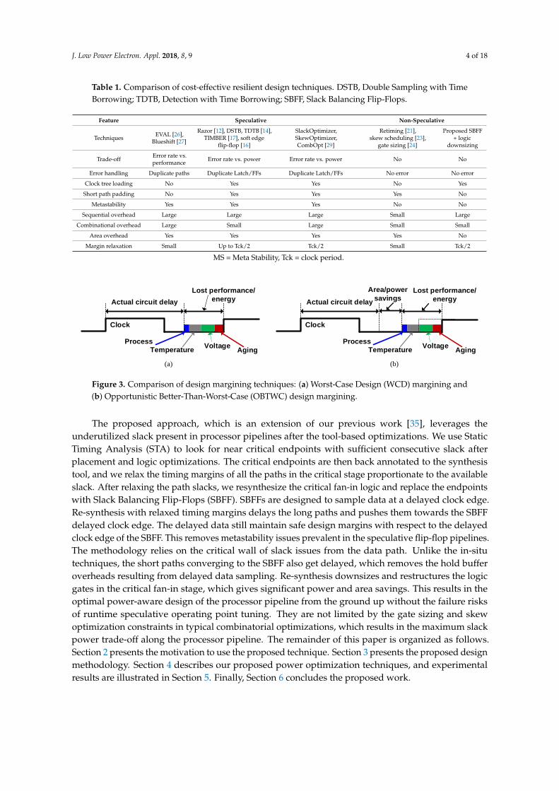
Table 1. Comparison of cost-effective resilient design techniques. DSTB, Double Sampling with TimeBorrowing; TDTB, Detection with Time Borrowing; SBFF, Slack Balancing Flip-Flops.
Feature Speculative Non-Speculative
Techniques EVAL [26],Blueshift [27]
Razor [12], DSTB, TDTB [14],TIMBER [17], soft edge
flip-flop [16]
SlackOptimizer,SkewOptimizer,CombOpt [29]
Retiming [21],skew scheduling [23],
gate sizing [24]
Proposed SBFF+ logic
downsizing
Trade-off Error rate vs.performance Error rate vs. power Error rate vs. power No No
Error handling Duplicate paths Duplicate Latch/FFs Duplicate Latch/FFs No error No error
Clock tree loading No Yes Yes No Yes
Short path padding No Yes Yes Yes No
Metastability Yes Yes Yes No No
Sequential overhead Large Large Large Small Large
Combinational overhead Large Small Large Small Small
Area overhead Yes Yes Yes Yes No
Margin relaxation Small Up to Tck/2 Tck/2 Small Tck/2
MS = Meta Stability, Tck = clock period.
J. Low Power Electron. Appl. 2018, 7, x 4 of 18
Table 1. Comparison of cost-effective resilient design techniques. DSTB, Double Sampling with Time Borrowing; TDTB, Detection with Time Borrowing; SBFF, Slack Balancing Flip-Flops.
Feature Speculative Non-Speculative
Techniques EVAL [26],
Blueshift [27]
Razor [12], DSTB, TDTB [14],
TIMBER [17], soft edge flip-flop [16]
SlackOptimizer, SkewOptimizer, CombOpt [29]
Retiming [21], skew scheduling [23], gate sizing
[24]
Proposed SBFF + logic
downsizing
Trade-off Error rate vs. performance
Error rate vs. power
Error rate vs. power No No
Error handling Duplicate
paths Duplicate Latch/FFs
Duplicate Latch/FFs No error No error
Clock tree loading
No Yes Yes No Yes
Short path padding
No Yes Yes Yes No
Metastability Yes Yes Yes No No Sequential overhead Large Large Large Small Large
Combinational overhead
Large Small Large Small Small
Area overhead Yes Yes Yes Yes No Margin
relaxation Small Up to Tck/2 Tck/2 Small Tck/2
MS = Meta Stability, Tck = clock period.
Figure 3. Comparison of design margining techniques: (a) Worst-Case Design (WCD) margining and (b) Opportunistic Better-Than-Worst-Case (OBTWC) design margining.
The proposed approach, which is an extension of our previous work [35], leverages the underutilized slack present in processor pipelines after the tool-based optimizations. We use Static Timing Analysis (STA) to look for near critical endpoints with sufficient consecutive slack after placement and logic optimizations. The critical endpoints are then back annotated to the synthesis tool, and we relax the timing margins of all the paths in the critical stage proportionate to the available slack. After relaxing the path slacks, we resynthesize the critical fan-in logic and replace the endpoints with Slack Balancing Flip-Flops (SBFF). SBFFs are designed to sample data at a delayed clock edge. Re-synthesis with relaxed timing margins delays the long paths and pushes them towards the SBFF delayed clock edge. The delayed data still maintain safe design margins with respect to the delayed clock edge of the SBFF. This removes metastability issues prevalent in the speculative flip-flop pipelines. The methodology relies on the critical wall of slack issues from the data path. Unlike the in-situ techniques, the short paths converging to the SBFF also get delayed, which removes the hold buffer overheads resulting from delayed data sampling. Re-synthesis downsizes and restructures the logic gates in the critical fan-in stage, which gives significant power and area savings. This results in the optimal power-aware design of the processor pipeline from the ground up without the failure risks of runtime speculative operating point tuning. They are not limited by the gate sizing and skew optimization constraints in typical combinatorial optimizations, which results in the maximum slack power trade-off along the processor pipeline. The remainder of this paper is organized as follows. Section 2 presents the motivation to use the proposed technique. Section 3 presents the proposed
Actual circuit delayLost performance/
energy
Clock
ProcessTemperature Voltage Aging
(a) (b)
Actual circuit delayLost performance/
energy
Clock
ProcessTemperature Voltage Aging
Area/power savings
Figure 3. Comparison of design margining techniques: (a) Worst-Case Design (WCD) margining and(b) Opportunistic Better-Than-Worst-Case (OBTWC) design margining.
The proposed approach, which is an extension of our previous work [35], leverages theunderutilized slack present in processor pipelines after the tool-based optimizations. We use StaticTiming Analysis (STA) to look for near critical endpoints with sufficient consecutive slack afterplacement and logic optimizations. The critical endpoints are then back annotated to the synthesistool, and we relax the timing margins of all the paths in the critical stage proportionate to the availableslack. After relaxing the path slacks, we resynthesize the critical fan-in logic and replace the endpointswith Slack Balancing Flip-Flops (SBFF). SBFFs are designed to sample data at a delayed clock edge.Re-synthesis with relaxed timing margins delays the long paths and pushes them towards the SBFFdelayed clock edge. The delayed data still maintain safe design margins with respect to the delayedclock edge of the SBFF. This removes metastability issues prevalent in the speculative flip-flop pipelines.The methodology relies on the critical wall of slack issues from the data path. Unlike the in-situtechniques, the short paths converging to the SBFF also get delayed, which removes the hold bufferoverheads resulting from delayed data sampling. Re-synthesis downsizes and restructures the logicgates in the critical fan-in stage, which gives significant power and area savings. This results in theoptimal power-aware design of the processor pipeline from the ground up without the failure risksof runtime speculative operating point tuning. They are not limited by the gate sizing and skewoptimization constraints in typical combinatorial optimizations, which results in the maximum slackpower trade-off along the processor pipeline. The remainder of this paper is organized as follows.Section 2 presents the motivation to use the proposed technique. Section 3 presents the proposed designmethodology. Section 4 describes our proposed power optimization techniques, and experimentalresults are illustrated in Section 5. Finally, Section 6 concludes the proposed work.

J. Low Power Electron. Appl. 2018, 8, 9 5 of 18
2. Motivation
Conventional design margining approaches are based on dynamic operating point tuning and insitu error correction to trade off power and reliability. The operating conditions are tuned adaptively tillPoint of First Failure (PoFF), which makes the near critical paths also timing critical. Figure 3 shows theeffect of voltage scaling on the slack histogram of critical paths in a processor pipeline. Figure 4a showsthe baseline designed for the worst case with a Worst Negative Slack (WNS) of 10 ps. However, withthe voltage scaling of 20 mV, 312 paths have negative slack, and the WNS becomes −600 ps (Figure 4b).Similarly, 985 paths have negative slack and the WNS becomes −700 ps when the supply voltage isscaled by 40 mV (Figure 4c). It is obvious that the paths with negative slack and the WNS increaseswith voltage scaling. The newly-created critical paths also need to be error resilient, which createshuge overheads in designs. Figure 5 plots the Total Negative Slack (TNS) of the processor pipelineagainst the voltage scaling steps. Voltage scaling down to Va does not increase TNS. TNS slightlyincreases between Va and Vb, but can be managed using in situ error correction techniques. BeyondVb, TNS increases rapidly, and the increased number of critical paths makes the error correctioncost enormous. In the event of high error rates, the system frequency has to be halved to recoverfrom errors.
Traditional timing-driven optimizations focus on the combinational logic and do not supportany tradeoffs between the logic paths separated by sequential elements. This results in a slackimbalance in the pipeline stages. Based on our timing analysis of a delay-optimized processor pipeline,we found that there is significant slack rebalance opportunity between the critical pipe_1 paths and theconsecutive pipe_2 paths, as shown in Figure 6. We leverage this slack to relax and resynthesize thecritical fan-in logic and sample the resulting delayed inputs using a slack balancing flip-flop. Insteadof reducing design margins at runtime using adaptive techniques, the proposed approach downsizesthe critical fan-in logic of the pipeline for power savings. Worst-case design margins are still met withrespect to the delayed clock edge of the slack balancing flip-flop, which helps to eliminate metastabilityissue faced by adaptive in situ error correction schemes. Moreover, we also relax the short paths bythe same design margin, which eliminates the need for SBFF-induced short path buffer insertionslater in the design flow. In contrast to the existing slack redistribution techniques [21–27], we insertintentional clock delays to fully balance the available slack at the critical endpoints and redesign thewhole critical logic stage with the relaxed time constraints. This results in a pipeline optimized forlow power without the need for runtime voltage speculation, which is vulnerable to critical operatingpoint behavior. The proposed method designs the processor to handle worst-case PVT margins. Logicdownsizing pushes the critical data towards the delayed clock edge, which is timed to maintainworst-case margins with respect to the delayed clock edge. This makes the design resistant to staticand dynamic variations similar to traditional worst-case corner designs, but with lower power andarea. Razor and TIMBER depend on runtime voltage and frequency scaling to reclaim the designmargins associated with dynamic variations. Therefore, they require error handling circuitry and needto tune the voltage or frequency back to the worst case operating corner depending on the error rate.There is a significant risk and architectural latency involved in this runtime adaption, especially whenthe error rate is high.

J. Low Power Electron. Appl. 2018, 8, 9 6 of 18J. Low Power Electron. Appl. 2018, 7, x 6 of 18
0
50
100
150
200
250
300
0 10 20 30 40 50 60 70 80 90 100
Slack (ps)
# o
f pat
hs
Slack histogram at Vworstcase
0
20
40
60
80
100
120
-600 -500 -400 -300 -200 -100 0 100Slack (ps)
# o
f pat
hs
Slack histogram with 20mV voltage scaling
Slack (ps)
# o
f pat
hs
Slack histogram with 40mV voltage scaling
(a) (b) (c)
0
50
100
150
200
250
300
350
400
-700 -600 -500 -400 -300 -200 -100 0 100
Figure 4. Slack histogram of the processor pipeline (a) in the worst case, (b) with 20-mV voltage scaling and (c) with 40-mV voltage scaling.
TNS
(ns)
0
50
100
150
200
250
300
350
400
450
10 15 20 25 30 35 40
Voltage scaling step (mV)
va vb
Figure 5. Cost of resilience and voltage scaling trade-off.
0
5
10
15
20
25
30
35
0 10 20 30 40 50 60 70 80 90 100
# of
pat
hs
Pipe1_slack (ps)
Fetch stage
0
5
10
15
20
25
30
35
40
45
0 500 1000 1500 2000 2500 3000 3500 4000 4500
# of
pat
hs
Pipe2_slack (ps)
Fetch stage
0
0.5
1
1.5
2
2.5
0 10 20 30 40 50 60 70 80 90 100
# of
pat
hs
Pipe1_slack (ps)
Decode stage
0
2
4
6
8
10
12
14
0 500 1000 1500 2000 2500 3000 3500 4000 4500
# of
pat
hs
Pipe2_slack (ps)
Decode stage
0
20
40
60
80
100
120
0 10 20 30 40 50 60 70 80 90 100
# of
pat
hs
Pipe1_slack (ps)
Execute stage
# of
pat
hs
Pipe2_slack (ps)
Execute stage
0
20
40
60
80
100
120
140
160
180
200
0 500 1000 1500 2000 2500 3000 3500 4000 4500
Figure 6. Critical path slacks (pipe_1) and consecutive stage slacks (pipe_2) of the processor.
3. Proposed Variation Tolerant Pipeline Design
3.1. Slack Balancing Principle
To explain slack balancing, we consider a small circuit as shown in Figure 7 with four registers. The timing graph shows nodes corresponding to the registers and edges corresponding to the combinational paths. The maximum delay for each combinational path is shown beside the edges. This circuit is optimized for a minimum feasible clock period T = 11. The combinational path (d, b)
Figure 4. Slack histogram of the processor pipeline (a) in the worst case, (b) with 20-mV voltage scalingand (c) with 40-mV voltage scaling.
J. Low Power Electron. Appl. 2018, 7, x 6 of 18
0
50
100
150
200
250
300
0 10 20 30 40 50 60 70 80 90 100
Slack (ps)
# o
f pat
hs
Slack histogram at Vworstcase
0
20
40
60
80
100
120
-600 -500 -400 -300 -200 -100 0 100Slack (ps)
# o
f pat
hs
Slack histogram with 20mV voltage scaling
Slack (ps)
# o
f pat
hs
Slack histogram with 40mV voltage scaling
(a) (b) (c)
0
50
100
150
200
250
300
350
400
-700 -600 -500 -400 -300 -200 -100 0 100
Figure 4. Slack histogram of the processor pipeline (a) in the worst case, (b) with 20-mV voltage scaling and (c) with 40-mV voltage scaling.
TNS
(ns)
0
50
100
150
200
250
300
350
400
450
10 15 20 25 30 35 40
Voltage scaling step (mV)
va vb
Figure 5. Cost of resilience and voltage scaling trade-off.
0
5
10
15
20
25
30
35
0 10 20 30 40 50 60 70 80 90 100
# of
pat
hs
Pipe1_slack (ps)
Fetch stage
0
5
10
15
20
25
30
35
40
45
0 500 1000 1500 2000 2500 3000 3500 4000 4500
# of
pat
hs
Pipe2_slack (ps)
Fetch stage
0
0.5
1
1.5
2
2.5
0 10 20 30 40 50 60 70 80 90 100
# of
pat
hs
Pipe1_slack (ps)
Decode stage
0
2
4
6
8
10
12
14
0 500 1000 1500 2000 2500 3000 3500 4000 4500
# of
pat
hs
Pipe2_slack (ps)
Decode stage
0
20
40
60
80
100
120
0 10 20 30 40 50 60 70 80 90 100
# of
pat
hs
Pipe1_slack (ps)
Execute stage
# of
pat
hs
Pipe2_slack (ps)
Execute stage
0
20
40
60
80
100
120
140
160
180
200
0 500 1000 1500 2000 2500 3000 3500 4000 4500
Figure 6. Critical path slacks (pipe_1) and consecutive stage slacks (pipe_2) of the processor.
3. Proposed Variation Tolerant Pipeline Design
3.1. Slack Balancing Principle
To explain slack balancing, we consider a small circuit as shown in Figure 7 with four registers. The timing graph shows nodes corresponding to the registers and edges corresponding to the combinational paths. The maximum delay for each combinational path is shown beside the edges. This circuit is optimized for a minimum feasible clock period T = 11. The combinational path (d, b)
Figure 5. Cost of resilience and voltage scaling trade-off.
J. Low Power Electron. Appl. 2018, 7, x 6 of 18
0
50
100
150
200
250
300
0 10 20 30 40 50 60 70 80 90 100
Slack (ps)
# o
f pat
hs
Slack histogram at Vworstcase
0
20
40
60
80
100
120
-600 -500 -400 -300 -200 -100 0 100Slack (ps)
# o
f pat
hs
Slack histogram with 20mV voltage scaling
Slack (ps)
# o
f pat
hs
Slack histogram with 40mV voltage scaling
(a) (b) (c)
0
50
100
150
200
250
300
350
400
-700 -600 -500 -400 -300 -200 -100 0 100
Figure 4. Slack histogram of the processor pipeline (a) in the worst case, (b) with 20-mV voltage scaling and (c) with 40-mV voltage scaling.
TNS
(ns)
0
50
100
150
200
250
300
350
400
450
10 15 20 25 30 35 40
Voltage scaling step (mV)
va vb
Figure 5. Cost of resilience and voltage scaling trade-off.
0
5
10
15
20
25
30
35
0 10 20 30 40 50 60 70 80 90 100
# of
pat
hs
Pipe1_slack (ps)
Fetch stage
0
5
10
15
20
25
30
35
40
45
0 500 1000 1500 2000 2500 3000 3500 4000 4500
# of
pat
hs
Pipe2_slack (ps)
Fetch stage
0
0.5
1
1.5
2
2.5
0 10 20 30 40 50 60 70 80 90 100
# of
pat
hs
Pipe1_slack (ps)
Decode stage
0
2
4
6
8
10
12
14
0 500 1000 1500 2000 2500 3000 3500 4000 4500
# of
pat
hs
Pipe2_slack (ps)
Decode stage
0
20
40
60
80
100
120
0 10 20 30 40 50 60 70 80 90 100
# of
pat
hs
Pipe1_slack (ps)
Execute stage
# of
pat
hs
Pipe2_slack (ps)
Execute stage
0
20
40
60
80
100
120
140
160
180
200
0 500 1000 1500 2000 2500 3000 3500 4000 4500
Figure 6. Critical path slacks (pipe_1) and consecutive stage slacks (pipe_2) of the processor.
3. Proposed Variation Tolerant Pipeline Design
3.1. Slack Balancing Principle
To explain slack balancing, we consider a small circuit as shown in Figure 7 with four registers. The timing graph shows nodes corresponding to the registers and edges corresponding to the combinational paths. The maximum delay for each combinational path is shown beside the edges. This circuit is optimized for a minimum feasible clock period T = 11. The combinational path (d, b)
Figure 6. Critical path slacks (pipe_1) and consecutive stage slacks (pipe_2) of the processor.
3. Proposed Variation Tolerant Pipeline Design
3.1. Slack Balancing Principle
To explain slack balancing, we consider a small circuit as shown in Figure 7 with four registers.The timing graph shows nodes corresponding to the registers and edges corresponding to thecombinational paths. The maximum delay for each combinational path is shown beside the edges.This circuit is optimized for a minimum feasible clock period T = 11. The combinational path (d, b) has

J. Low Power Electron. Appl. 2018, 8, 9 7 of 18
a maximum delay of 11. In this critical path, time can be borrowed from the consecutive stage (b, d)whose delay is nine. We replace the flip-flop b by the SBFF with a clock delay equal to the slack presentin the consecutive stage (b, d), which is two. Now, for the same clock period T = 11, we have an extramargin of two in the fan-in paths (a, b) and (d, b). The extra margin is used to relax and downsize thelogic in the fan-in paths, making sure it does not create other timing violations. This procedure alsodelays the short paths along the critical fan-in logic, thus eliminating the need for additional bufferscompared to other timing speculation techniques.
J. Low Power Electron. Appl. 2018, 7, x 7 of 18
has a maximum delay of 11. In this critical path, time can be borrowed from the consecutive stage (b, d) whose delay is nine. We replace the flip-flop b by the SBFF with a clock delay equal to the slack present in the consecutive stage (b, d), which is two. Now, for the same clock period T = 11, we have an extra margin of two in the fan-in paths (a, b) and (d, b). The extra margin is used to relax and downsize the logic in the fan-in paths, making sure it does not create other timing violations. This procedure also delays the short paths along the critical fan-in logic, thus eliminating the need for additional buffers compared to other timing speculation techniques.
911997
5
9
6a b
c d
9
2 7a
5 6b
45
d
c
Figure 7. A circuit example and timing graph to explain slack balancing.
We compare the proposed technique with existing speculative error correction schemes. Figure 8a shows conceptually how the slack margins are relaxed in a typical voltage scaling-based error resilience scheme. We consider four timing paths P1, P2, P3 and P4 with different slack margins. Here, we assume P3 to be a part of a non-critical fan-in logic and P1, P2 and P4 in the critical fan-in logic with P1 being a critical short path. Energy can be reduced by scaling the supply voltage, which increases the delay along these paths. The timing speculation window for a typical speculative error resilience scheme is Tclk/2. Therefore, the paths are allowed to relax the delay margins by Tclk/2, as shown in Figure 8b. Voltage scaling is done beyond PoFF until the critical operating voltage near critical path P3 also becomes timing critical as depicted in Figure 8c. Moreover, runtime voltage scaling causes the inputs to change close to the clock edges, creating metastability issues. They also require additional buffers along P1 to ensure that it will not corrupt the delayed data and hence the error generated. Even if timing speculation is not done till Tclk/2, we still need to insert buffers for an equivalent delay of Tclk/2 to ensure that the error signal is not corrupted. Unless we use a fine-grain voltage scaling, even non-critical paths like P3 will become critical. Furthermore, for performance-driven design margin relaxation techniques, the slack relaxations are suboptimal as shown in Figure 9b. Frequency scaling results in new critical path formations in P3, as shown in Figure 9c, which makes the scaling bounded.
Slack margin Error correction FF allows speculation by Tclk/2
Voltage scaled till critical operating point
unused slack margin(b)(a) (c)
P1
P2
P3
P4
new critical path
Figure 8. Speculative power-aware flip-flop: (a) slack margin at sign off, (b) slack margin relaxed with timing speculation flip-flop and (c) slack margin traded off with power. P1, Path 1.
Figure 7. A circuit example and timing graph to explain slack balancing.
We compare the proposed technique with existing speculative error correction schemes.Figure 8a shows conceptually how the slack margins are relaxed in a typical voltage scaling-basederror resilience scheme. We consider four timing paths P1, P2, P3 and P4 with different slack margins.Here, we assume P3 to be a part of a non-critical fan-in logic and P1, P2 and P4 in the critical fan-in logicwith P1 being a critical short path. Energy can be reduced by scaling the supply voltage, which increasesthe delay along these paths. The timing speculation window for a typical speculative error resiliencescheme is Tclk/2. Therefore, the paths are allowed to relax the delay margins by Tclk/2, as shown inFigure 8b. Voltage scaling is done beyond PoFF until the critical operating voltage near critical path P3also becomes timing critical as depicted in Figure 8c. Moreover, runtime voltage scaling causes theinputs to change close to the clock edges, creating metastability issues. They also require additionalbuffers along P1 to ensure that it will not corrupt the delayed data and hence the error generated.Even if timing speculation is not done till Tclk/2, we still need to insert buffers for an equivalentdelay of Tclk/2 to ensure that the error signal is not corrupted. Unless we use a fine-grain voltagescaling, even non-critical paths like P3 will become critical. Furthermore, for performance-drivendesign margin relaxation techniques, the slack relaxations are suboptimal as shown in Figure 9b.Frequency scaling results in new critical path formations in P3, as shown in Figure 9c, which makesthe scaling bounded.
J. Low Power Electron. Appl. 2018, 7, x 7 of 18
has a maximum delay of 11. In this critical path, time can be borrowed from the consecutive stage (b, d) whose delay is nine. We replace the flip-flop b by the SBFF with a clock delay equal to the slack present in the consecutive stage (b, d), which is two. Now, for the same clock period T = 11, we have an extra margin of two in the fan-in paths (a, b) and (d, b). The extra margin is used to relax and downsize the logic in the fan-in paths, making sure it does not create other timing violations. This procedure also delays the short paths along the critical fan-in logic, thus eliminating the need for additional buffers compared to other timing speculation techniques.
911997
5
9
6a b
c d
9
2 7a
5 6b
45
d
c
Figure 7. A circuit example and timing graph to explain slack balancing.
We compare the proposed technique with existing speculative error correction schemes. Figure 8a shows conceptually how the slack margins are relaxed in a typical voltage scaling-based error resilience scheme. We consider four timing paths P1, P2, P3 and P4 with different slack margins. Here, we assume P3 to be a part of a non-critical fan-in logic and P1, P2 and P4 in the critical fan-in logic with P1 being a critical short path. Energy can be reduced by scaling the supply voltage, which increases the delay along these paths. The timing speculation window for a typical speculative error resilience scheme is Tclk/2. Therefore, the paths are allowed to relax the delay margins by Tclk/2, as shown in Figure 8b. Voltage scaling is done beyond PoFF until the critical operating voltage near critical path P3 also becomes timing critical as depicted in Figure 8c. Moreover, runtime voltage scaling causes the inputs to change close to the clock edges, creating metastability issues. They also require additional buffers along P1 to ensure that it will not corrupt the delayed data and hence the error generated. Even if timing speculation is not done till Tclk/2, we still need to insert buffers for an equivalent delay of Tclk/2 to ensure that the error signal is not corrupted. Unless we use a fine-grain voltage scaling, even non-critical paths like P3 will become critical. Furthermore, for performance-driven design margin relaxation techniques, the slack relaxations are suboptimal as shown in Figure 9b. Frequency scaling results in new critical path formations in P3, as shown in Figure 9c, which makes the scaling bounded.
Slack margin Error correction FF allows speculation by Tclk/2
Voltage scaled till critical operating point
unused slack margin(b)(a) (c)
P1
P2
P3
P4
new critical path
Figure 8. Speculative power-aware flip-flop: (a) slack margin at sign off, (b) slack margin relaxed with timing speculation flip-flop and (c) slack margin traded off with power. P1, Path 1. Figure 8. Speculative power-aware flip-flop: (a) slack margin at sign off; (b) slack margin relaxed withtiming speculation flip-flop and (c) slack margin traded off with power. P1, Path 1.

J. Low Power Electron. Appl. 2018, 8, 9 8 of 18J. Low Power Electron. Appl. 2018, 7, x 8 of 18
Slack margin clock skew and gate size tuning ; slack relaxed <
Tclk/2Frequency scaled till
critical operating point
unused slack margin(b)(a) (c)
P1
P2
P3
P4
new critical path
Figure 9. Performance-aware optimizations: (a) slack margin at sign off, (b) slack margin relaxed with clock skew scheduling and gate sizing and (c) slack margin traded off with frequency.
In our proposed technique, we use static time borrowing to trade off slack margin for power and area gains. Figure 10a shows the slack margins of the baseline worst-case design. We look for positive slack in the pipeline stages and replace the critical endpoints with SBFFs, which borrows a time TB proportional to the available slacks as depicted in Figure 10b. As a result, the critical fan-in paths P1, P2 and P4 are relaxed by TB. We re-synthesize the pipeline to downsize the fan-in logic of SBFF for power and area reductions (Figure 10c). After resizing the logic, timing closure is done on the data paths with respect to the delayed clock edges of SBFF. Our approach is deterministic and non-speculative, unlike the usual dynamic operating point scaling techniques. Safe design margins are kept with respect to the delayed clock edge of the SBFF, which prevents metastability issues in the pipeline. Unlike conventional resilience schemes, the short path P1 is also delayed by the corresponding TB window TB1. This eliminates the need for additional short path buffers along P1 to prevent it from corrupting the delayed data. Note that the time borrow window TB is fully utilized for power and area reduction compared to other optimization techniques. Unlike clock skew scheduling, which is mostly used for performance enhancements, the proposed method targets critical logic power minimization by utilizing maximum available slack to downsize all logic paths in the critical stage.
Slack margin SBFF relaxes slack
margin by available slack up to Tclk/2
TB1
TB3
TB4
Slack margin used to downsize logic
(b)(a) (c)
P1
P2
P3
P4
Figure 10. Proposed SBFF: (a) slack margin at sign off, (b) slack margin relaxed with SBFF and (c) slack margin used to downsize logic.
3.2. Slack Balancing Flip-Flop
The SBFF and the timing diagram are illustrated in Figure 11. SBFF is a simplified version of TIMBER [17] without any error propagation logic. SBFF consists of the main latch, a shadow latch and a clock control circuit. The data path has a main latch and a slave latch forming an edge-triggered master-slave flip-flop. The proposed optimization technique downsizes the SBFF input logic for power reduction. This delays the input data signal DATA, which is detected by the shadow latch using a Delayed Clock (DCK). The delay amount decides the design margin improvement. The input to the slave latch is switched between the master path and the shadow path using the control signals (P0 and P1) to ensure that the delayed data pass through the slave latch. As shown in Figure 11, the main latch samples the input data and transfers them to the output (Q) at the positive Clock (CK) edge when TG0 is closed and TG1 is open. Similarly, the slave latch samples the data and passes them to the output at the Delayed Clock edge (DCK) when TG1 is closed and TG0 is open. The data in the
Figure 9. Performance-aware optimizations: (a) slack margin at sign off; (b) slack margin relaxed withclock skew scheduling and gate sizing and (c) slack margin traded off with frequency.
In our proposed technique, we use static time borrowing to trade off slack margin for powerand area gains. Figure 10a shows the slack margins of the baseline worst-case design. We look forpositive slack in the pipeline stages and replace the critical endpoints with SBFFs, which borrowsa time TB proportional to the available slacks as depicted in Figure 10b. As a result, the critical fan-inpaths P1, P2 and P4 are relaxed by TB. We re-synthesize the pipeline to downsize the fan-in logic ofSBFF for power and area reductions (Figure 10c). After resizing the logic, timing closure is done onthe data paths with respect to the delayed clock edges of SBFF. Our approach is deterministic andnon-speculative, unlike the usual dynamic operating point scaling techniques. Safe design marginsare kept with respect to the delayed clock edge of the SBFF, which prevents metastability issuesin the pipeline. Unlike conventional resilience schemes, the short path P1 is also delayed by thecorresponding TB window TB1. This eliminates the need for additional short path buffers along P1 toprevent it from corrupting the delayed data. Note that the time borrow window TB is fully utilized forpower and area reduction compared to other optimization techniques. Unlike clock skew scheduling,which is mostly used for performance enhancements, the proposed method targets critical logic powerminimization by utilizing maximum available slack to downsize all logic paths in the critical stage.
J. Low Power Electron. Appl. 2018, 7, x 8 of 18
Slack margin clock skew and gate size tuning ; slack relaxed <
Tclk/2Frequency scaled till
critical operating point
unused slack margin(b)(a) (c)
P1
P2
P3
P4
new critical path
Figure 9. Performance-aware optimizations: (a) slack margin at sign off, (b) slack margin relaxed with clock skew scheduling and gate sizing and (c) slack margin traded off with frequency.
In our proposed technique, we use static time borrowing to trade off slack margin for power and area gains. Figure 10a shows the slack margins of the baseline worst-case design. We look for positive slack in the pipeline stages and replace the critical endpoints with SBFFs, which borrows a time TB proportional to the available slacks as depicted in Figure 10b. As a result, the critical fan-in paths P1, P2 and P4 are relaxed by TB. We re-synthesize the pipeline to downsize the fan-in logic of SBFF for power and area reductions (Figure 10c). After resizing the logic, timing closure is done on the data paths with respect to the delayed clock edges of SBFF. Our approach is deterministic and non-speculative, unlike the usual dynamic operating point scaling techniques. Safe design margins are kept with respect to the delayed clock edge of the SBFF, which prevents metastability issues in the pipeline. Unlike conventional resilience schemes, the short path P1 is also delayed by the corresponding TB window TB1. This eliminates the need for additional short path buffers along P1 to prevent it from corrupting the delayed data. Note that the time borrow window TB is fully utilized for power and area reduction compared to other optimization techniques. Unlike clock skew scheduling, which is mostly used for performance enhancements, the proposed method targets critical logic power minimization by utilizing maximum available slack to downsize all logic paths in the critical stage.
Slack margin SBFF relaxes slack
margin by available slack up to Tclk/2
TB1
TB3
TB4
Slack margin used to downsize logic
(b)(a) (c)
P1
P2
P3
P4
Figure 10. Proposed SBFF: (a) slack margin at sign off, (b) slack margin relaxed with SBFF and (c) slack margin used to downsize logic.
3.2. Slack Balancing Flip-Flop
The SBFF and the timing diagram are illustrated in Figure 11. SBFF is a simplified version of TIMBER [17] without any error propagation logic. SBFF consists of the main latch, a shadow latch and a clock control circuit. The data path has a main latch and a slave latch forming an edge-triggered master-slave flip-flop. The proposed optimization technique downsizes the SBFF input logic for power reduction. This delays the input data signal DATA, which is detected by the shadow latch using a Delayed Clock (DCK). The delay amount decides the design margin improvement. The input to the slave latch is switched between the master path and the shadow path using the control signals (P0 and P1) to ensure that the delayed data pass through the slave latch. As shown in Figure 11, the main latch samples the input data and transfers them to the output (Q) at the positive Clock (CK) edge when TG0 is closed and TG1 is open. Similarly, the slave latch samples the data and passes them to the output at the Delayed Clock edge (DCK) when TG1 is closed and TG0 is open. The data in the
Figure 10. Proposed SBFF: (a) slack margin at sign off, (b) slack margin relaxed with SBFF and (c) slackmargin used to downsize logic.
3.2. Slack Balancing Flip-Flop
The SBFF and the timing diagram are illustrated in Figure 11. SBFF is a simplified version ofTIMBER [17] without any error propagation logic. SBFF consists of the main latch, a shadow latch anda clock control circuit. The data path has a main latch and a slave latch forming an edge-triggeredmaster-slave flip-flop. The proposed optimization technique downsizes the SBFF input logic for powerreduction. This delays the input data signal DATA, which is detected by the shadow latch usinga Delayed Clock (DCK). The delay amount decides the design margin improvement. The input tothe slave latch is switched between the master path and the shadow path using the control signals(P0 and P1) to ensure that the delayed data pass through the slave latch. As shown in Figure 11,the main latch samples the input data and transfers them to the output (Q) at the positive Clock (CK)edge when TG0 is closed and TG1 is open. Similarly, the slave latch samples the data and passes

J. Low Power Electron. Appl. 2018, 8, 9 9 of 18
them to the output at the Delayed Clock edge (DCK) when TG1 is closed and TG0 is open. The datain the master latch are compared with those in the slave latch by an XOR gate. The xor gate outputsignal XOR_OUT becomes ‘1’ when they are different. Figure 12 shows the simulation results ofthe SBFF. XOR_OUT is sampled by P1 to filter any glitches and fake transitions in the SBFF andgenerates a sampled signal XOR_OUT_SAMPLED. It shows that the delayed DATA are detected by thedelayed clock DCK of the SBFF. The XOR output is also used to generate the monitor signal ACTIVITYMONITOR. Depending on whether a data transition happens in the clock cycle, the master latch andshadow latch will sample the same value or a different value. This will be handy in the pre-silicon orpost-silicon stage to disable the time borrowing in the event of low data activity rates, which results infurther power reduction. In Figure 13a, the monitor signal is triggered only once, which shows a lowdata rate. The monitor signal is triggered continuously in all the clock cycles as shown in Figure 13bfor high data rates.
J. Low Power Electron. Appl. 2018, 7, x 9 of 18
master latch are compared with those in the slave latch by an XOR gate. The xor gate output signal XOR_OUT becomes ‘1’ when they are different. Figure 12 shows the simulation results of the SBFF. XOR_OUT is sampled by P1 to filter any glitches and fake transitions in the SBFF and generates a sampled signal XOR_OUT_SAMPLED. It shows that the delayed DATA are detected by the delayed clock DCK of the SBFF. The XOR output is also used to generate the monitor signal ACTIVITY MONITOR. Depending on whether a data transition happens in the clock cycle, the master latch and shadow latch will sample the same value or a different value. This will be handy in the pre-silicon or post-silicon stage to disable the time borrowing in the event of low data activity rates, which results in further power reduction. In Figure 13a, the monitor signal is triggered only once, which shows a low data rate. The monitor signal is triggered continuously in all the clock cycles as shown in Figure 13b for high data rates.
DATA
R
CK
CK
DCK
DCK
CK
CK
DCK
DCK
R
CK
CK
Q
P0
P1
P0
P1
P1
ACTIVITY MONITOR
L0
L1
XOR_OUT
Main Latch
Shadow Latch DCK
P0
P1
P0
P1
CK
TG0
TG1
(a)
EN
TG2
L0 samples DATA
TG0 open
L1 samples DATA
L0 drives input to output
L1 drives input to output
TG1 openCK
DCK
(b)
Slave Latch
L0: Main LatchL1: Slave Latch
Figure 11. (a) SBFF and (b) timing diagram. DCK, Delayed Clock.
TIME (a.u.)
Glitch
Fake transition
Delayed data detectionDATA
Q
CK
DCK
LATCH0
LATCH1
XOR_OUT
XOR_OUT_SAMPLED
Delayed clock edge
Figure 12. SBFF simulation result.
CK
DCK
D
ACTIVITY MONITOR
CK
DCK
D
ACTIVITY MONITOR
(a) (b) Figure 13. Data activity monitoring in SBFF. (a) Intermittent triggering of the activity monitor with low data activity and (b) continuous triggering of activity monitor with high data activity.
Figure 11. (a) SBFF and (b) timing diagram. DCK, Delayed Clock.
J. Low Power Electron. Appl. 2018, 7, x 9 of 18
master latch are compared with those in the slave latch by an XOR gate. The xor gate output signal XOR_OUT becomes ‘1’ when they are different. Figure 12 shows the simulation results of the SBFF. XOR_OUT is sampled by P1 to filter any glitches and fake transitions in the SBFF and generates a sampled signal XOR_OUT_SAMPLED. It shows that the delayed DATA are detected by the delayed clock DCK of the SBFF. The XOR output is also used to generate the monitor signal ACTIVITY MONITOR. Depending on whether a data transition happens in the clock cycle, the master latch and shadow latch will sample the same value or a different value. This will be handy in the pre-silicon or post-silicon stage to disable the time borrowing in the event of low data activity rates, which results in further power reduction. In Figure 13a, the monitor signal is triggered only once, which shows a low data rate. The monitor signal is triggered continuously in all the clock cycles as shown in Figure 13b for high data rates.
DATA
R
CK
CK
DCK
DCK
CK
CK
DCK
DCK
R
CK
CK
Q
P0
P1
P0
P1
P1
ACTIVITY MONITOR
L0
L1
XOR_OUT
Main Latch
Shadow Latch DCK
P0
P1
P0
P1
CK
TG0
TG1
(a)
EN
TG2
L0 samples DATA
TG0 open
L1 samples DATA
L0 drives input to output
L1 drives input to output
TG1 openCK
DCK
(b)
Slave Latch
L0: Main LatchL1: Slave Latch
Figure 11. (a) SBFF and (b) timing diagram. DCK, Delayed Clock.
TIME (a.u.)
Glitch
Fake transition
Delayed data detectionDATA
Q
CK
DCK
LATCH0
LATCH1
XOR_OUT
XOR_OUT_SAMPLED
Delayed clock edge
Figure 12. SBFF simulation result.
CK
DCK
D
ACTIVITY MONITOR
CK
DCK
D
ACTIVITY MONITOR
(a) (b) Figure 13. Data activity monitoring in SBFF. (a) Intermittent triggering of the activity monitor with low data activity and (b) continuous triggering of activity monitor with high data activity.
Figure 12. SBFF simulation result.
J. Low Power Electron. Appl. 2018, 7, x 9 of 18
master latch are compared with those in the slave latch by an XOR gate. The xor gate output signal XOR_OUT becomes ‘1’ when they are different. Figure 12 shows the simulation results of the SBFF. XOR_OUT is sampled by P1 to filter any glitches and fake transitions in the SBFF and generates a sampled signal XOR_OUT_SAMPLED. It shows that the delayed DATA are detected by the delayed clock DCK of the SBFF. The XOR output is also used to generate the monitor signal ACTIVITY MONITOR. Depending on whether a data transition happens in the clock cycle, the master latch and shadow latch will sample the same value or a different value. This will be handy in the pre-silicon or post-silicon stage to disable the time borrowing in the event of low data activity rates, which results in further power reduction. In Figure 13a, the monitor signal is triggered only once, which shows a low data rate. The monitor signal is triggered continuously in all the clock cycles as shown in Figure 13b for high data rates.
DATA
R
CK
CK
DCK
DCK
CK
CK
DCK
DCK
R
CK
CK
Q
P0
P1
P0
P1
P1
ACTIVITY MONITOR
L0
L1
XOR_OUT
Main Latch
Shadow Latch DCK
P0
P1
P0
P1
CK
TG0
TG1
(a)
EN
TG2
L0 samples DATA
TG0 open
L1 samples DATA
L0 drives input to output
L1 drives input to output
TG1 openCK
DCK
(b)
Slave Latch
L0: Main LatchL1: Slave Latch
Figure 11. (a) SBFF and (b) timing diagram. DCK, Delayed Clock.
TIME (a.u.)
Glitch
Fake transition
Delayed data detectionDATA
Q
CK
DCK
LATCH0
LATCH1
XOR_OUT
XOR_OUT_SAMPLED
Delayed clock edge
Figure 12. SBFF simulation result.
CK
DCK
D
ACTIVITY MONITOR
CK
DCK
D
ACTIVITY MONITOR
(a) (b) Figure 13. Data activity monitoring in SBFF. (a) Intermittent triggering of the activity monitor with low data activity and (b) continuous triggering of activity monitor with high data activity.
Figure 13. Data activity monitoring in SBFF. (a) Intermittent triggering of the activity monitor with lowdata activity and (b) continuous triggering of activity monitor with high data activity.

J. Low Power Electron. Appl. 2018, 8, 9 10 of 18
3.3. Pipeline Design Flow Using SBFF
We use standard CAD tools and custom add-on scripts for SBFF insertion and logic optimizationfor the proposed pipeline design. A standard cell library with 20 different flavors of SBFFs wasdeveloped using library characterization tools to replace the normal flip-flops. The library has foursets of non-scan flip-flops with two different drive strengths and four sets of scan flip-flops with threedifferent drive strengths. Custom scripts are used to enable slack analysis, time budgeting and SBFFreplacement. Figure 14 shows the proposed design flow using SBFF. It starts with filtering the criticalpaths based on post-placement and optimization STA results. In this work, we consider ~10% ofthe total flip-flops that are most critical, whose slack is less than 2% of the clock period. In the nextstep, we search for the critical endpoints with sufficient consecutive slacks. These endpoints are backannotated to the synthesis engine. The timing for all the critical fan-in paths is relaxed proportionateto the available slack. The pipeline is then resynthesized with the new timing constraints. We thenreplace the endpoints by SBFFs and run the placement and clock tree. The clock delays for the SBFFsare inserted after the clock tree is built. This helps to preserve the traditional tool-based optimizations.We limit the inserted clock delay to TB1 = Tclk/8, TB2 = 2Tclk/8, TB3 = 3Tclk/8 and TB4 = 4Tclk/8 forsimplicity. The pipeline is then signed off, keeping worst-case design margins.
J. Low Power Electron. Appl. 2018, 7, x 10 of 18
3.3. Pipeline Design Flow Using SBFF
We use standard CAD tools and custom add-on scripts for SBFF insertion and logic optimization for the proposed pipeline design. A standard cell library with 20 different flavors of SBFFs was developed using library characterization tools to replace the normal flip-flops. The library has four sets of non-scan flip-flops with two different drive strengths and four sets of scan flip-flops with three different drive strengths. Custom scripts are used to enable slack analysis, time budgeting and SBFF replacement. Figure 14 shows the proposed design flow using SBFF. It starts with filtering the critical paths based on post-placement and optimization STA results. In this work, we consider ~10% of the total flip-flops that are most critical, whose slack is less than 2% of the clock period. In the next step, we search for the critical endpoints with sufficient consecutive slacks. These endpoints are back annotated to the synthesis engine. The timing for all the critical fan-in paths is relaxed proportionate to the available slack. The pipeline is then resynthesized with the new timing constraints. We then replace the endpoints by SBFFs and run the placement and clock tree. The clock delays for the SBFFs are inserted after the clock tree is built. This helps to preserve the traditional tool-based optimizations. We limit the inserted clock delay to TB1 = Tclk/8, TB2 = 2Tclk/8, TB3 = 3Tclk/8 and TB4 = 4Tclk/8 for simplicity. The pipeline is then signed off, keeping worst-case design margins.
Report slackRTL & constraints Synthesize Place & optimize
design
Filter critical endpoints with
slack < Th
Report consecutive slack
of all endpoints
Relax stage1 logic of the endpoints
by TBSynthesize again
Place & optimize design
Clock tree synthesis
Replace critical endpoints with
SBFF
Route &sign off
end
Delay insertion for SBFFs
Filter endpoints with stage2 slack >
TB
SBFF insertion and timing correction
Figure 14. Design flow using SBFF.
3.4. Metastability and Hold Issues
Speculative techniques relax max delay and constrain min delay by Tclk/2. The max delay savings is minimal if we consider error handling and min delay overheads. For a typical speculative pipeline shown in Figure 15, the max delay, Tmax can be speculated up to Tclk/2 till the falling edge of the clock and is calculated as:
Tmax = Tclk + Tclk/2 − Tsu,clk-f , (1)
where Tsu,clk-f represents the setup timing of the speculative flip-flop clock falling edge. The effective max delay improvement Tmax,eff is limited by the critical operating point and is calculated as:
Tmax,eff = Tclk + Tcop − Tsu,clk-f , (2)
where Tcop represents the effective amount by which max delay is relaxed till the critical operating point. The min delay requirement, Tmin, for Razor is tightened by Tclk/2 and is calculated as:
Tmin = Tclk/2 + Th,clk-f , (3)
Figure 14. Design flow using SBFF.
3.4. Metastability and Hold Issues
Speculative techniques relax max delay and constrain min delay by Tclk/2. The max delay savingsis minimal if we consider error handling and min delay overheads. For a typical speculative pipelineshown in Figure 15, the max delay, Tmax can be speculated up to Tclk/2 till the falling edge of the clockand is calculated as:
Tmax = Tclk + Tclk/2 − Tsu,clk-f, (1)
where Tsu,clk-f represents the setup timing of the speculative flip-flop clock falling edge. The effectivemax delay improvement Tmax,eff is limited by the critical operating point and is calculated as:
Tmax,eff = Tclk + Tcop − Tsu,clk-f, (2)
where Tcop represents the effective amount by which max delay is relaxed till the critical operatingpoint. The min delay requirement, Tmin, for Razor is tightened by Tclk/2 and is calculated as:

J. Low Power Electron. Appl. 2018, 8, 9 11 of 18
Tmin = Tclk/2 + Th,clk-f, (3)
where Th,clk-f represents the hold timing requirement of the speculative clock falling edge.Thus, for a max delay improvement of Tcop, there is a min delay buffer overhead of Tclk/2.
J. Low Power Electron. Appl. 2018, 7, x 11 of 18
where Th,clk-f represents the hold timing requirement of the speculative clock falling edge. Thus, for a max delay improvement of Tcop, there is a min delay buffer overhead of Tclk/2.
(a)
MSFF Razor FF
tcomb
terr-path
out
errclk
tsu
tsuclk
clk
D
D
clk
out
tres
tcomb
tsu tclk2err
Tsu,clk-f
D
clk
err
(b) (c)tclk2out
Tsu,clk-r
terr-path+ tres
Figure 15. (a) Speculative flip-flop pipeline, (b) data path metastability and (c) error path metastability.
SBFF relaxes the max delay and tightens the min delay of the critical fan-in logic by TB proportional to the consecutive stage slack as shown in Figure 16. The SBFF max delay, Tmax,SBFF, is calculated as:
Tmax,SBFF = Tclk + TB − Tsu,clk_del-r , (4)
where Tsu,clk_del-r represents the setup time constraint with respect to SBFF delayed clock rising edge. The max delay improvement of TB gives extra room for power, area and performance improvement. For high performance designs, the extra margin can be used to scale frequency. For low power designs, the extra margin can be used to under design the logic to achieve power and area savings. The logic downsizing makes sure that the short path delay also increases by TB, thus eliminating the need for additional hold buffers. The SBFF min delay, Tmin,SBFF, is calculated as:
Tmin,SBFF = TB + Th,clk_del-r , (5)
where Th,clk_del-r represents the hold timing requirement with respect to the SBFF delayed clock edge. As long as the TB constraint is satisfied, the D input meets the worst-case setup timing of the delayed clock. This eliminates the need for error correction. We can represent the maximum delay constraint on TB as:
TBmax,SBFF ≤ Tclk/2 − Tsu,clk_del-r , (6)
Runtime dynamic timing speculation techniques have metastability risks at the clock edges along the data path and error path. Data path metastability will arise if D input changes too close to the positive clock edge due to voltage scaling or PVT variations, as depicted in Figure 15b. As a statistical measure of the reliability from metastable errors, we express the Mean time between failures, MTBFdata-path, as:
MTBFdata-path = exp(tres⁄τc)⁄(fdata. T0. fclk), (7)
Here, tres represents the resolution time to exit the metastable state; T0 is the metastability window; τc is the metastability resolution time constant; fdat is the frequency of data transition; and fclk is the clock frequency. The metastability resolution time tres can be calculated as:
tres = Tclk − tclk2out − tcomb − tsu, (8)
Here, tclk2out is the clock to output delay of the flip-flop; tcomb is the combinational logic delay of the succeeding stage; and tsu is the setup time constraint of the subsequent flip-flop as shown in Figure 15b. A higher tres amounts to better protection from metastable errors. For the speculative flip-flop, tclk2out is worse than the conventional flip-flops due to the redundant latch, which makes tres smaller. This introduces additional constraints on the combinational delay of the next pipeline stage. The error path is also prone to metastability because the dynamic voltage scaling pushes the data too close to the negative clock edge, as shown in Figure 15c. The corresponding mean time between failures, MTBFerr-path, is represented as:
MTBFerr-path = exp(tres⁄τc)⁄(fdata. T0. fclk), (9)
Figure 15. (a) Speculative flip-flop pipeline, (b) data path metastability and (c) error path metastability.
SBFF relaxes the max delay and tightens the min delay of the critical fan-in logic by TB proportionalto the consecutive stage slack as shown in Figure 16. The SBFF max delay, Tmax,SBFF, is calculated as:
Tmax,SBFF = Tclk + TB − Tsu,clk_del-r, (4)
where Tsu,clk_del-r represents the setup time constraint with respect to SBFF delayed clock rising edge.The max delay improvement of TB gives extra room for power, area and performance improvement.For high performance designs, the extra margin can be used to scale frequency. For low power designs,the extra margin can be used to under design the logic to achieve power and area savings. The logicdownsizing makes sure that the short path delay also increases by TB, thus eliminating the need foradditional hold buffers. The SBFF min delay, Tmin,SBFF, is calculated as:
Tmin,SBFF = TB + Th,clk_del-r, (5)
where Th,clk_del-r represents the hold timing requirement with respect to the SBFF delayed clock edge.As long as the TB constraint is satisfied, the D input meets the worst-case setup timing of the delayedclock. This eliminates the need for error correction. We can represent the maximum delay constrainton TB as:
TBmax,SBFF ≤ Tclk/2 − Tsu,clk_del-r, (6)
Runtime dynamic timing speculation techniques have metastability risks at the clock edgesalong the data path and error path. Data path metastability will arise if D input changes tooclose to the positive clock edge due to voltage scaling or PVT variations, as depicted in Figure 15b.As a statistical measure of the reliability from metastable errors, we express the Mean time betweenfailures, MTBFdata-path, as:
MTBFdata-path = exp(tres/τc)/(fdata. T0. fclk), (7)
Here, tres represents the resolution time to exit the metastable state; T0 is the metastability window;τc is the metastability resolution time constant; fdat is the frequency of data transition; and fclk is theclock frequency. The metastability resolution time tres can be calculated as:
tres = Tclk − tclk2out − tcomb − tsu, (8)
Here, tclk2out is the clock to output delay of the flip-flop; tcomb is the combinational logic delay ofthe succeeding stage; and tsu is the setup time constraint of the subsequent flip-flop as shown inFigure 15b. A higher tres amounts to better protection from metastable errors. For the speculative

J. Low Power Electron. Appl. 2018, 8, 9 12 of 18
flip-flop, tclk2out is worse than the conventional flip-flops due to the redundant latch, which makestres smaller. This introduces additional constraints on the combinational delay of the next pipeline stage.The error path is also prone to metastability because the dynamic voltage scaling pushes the datatoo close to the negative clock edge, as shown in Figure 15c. The corresponding mean time betweenfailures, MTBFerr-path, is represented as:
MTBFerr-path = exp(tres/τc)/(fdata. T0. fclk), (9)
Here, tres represents the resolution time to exit the metastable state; T0 is the metastability window;τc is the metastability resolution time constant; fdat is the frequency of data transition; and fclk is the clockfrequency, all with respect to the error path. The error path metastability can be fatal especially sincespeculative designs rely on the error signal timing for proper error recovery. Here, the metastabilityresolution time tres can be expressed as:
tres = Tclk − TB − tclk2err − tcomb − tsu, (10)
Here, tclk2err is the clock to output delay for the error output signal with respect to the negativeclock edge. As shown in Figure 15c, the tres window for the error path is too small, and this putsadditional constraints on the error path delay terr-path. Resolution time can extend up to three clockcycles, which means the error signal will take three clock cycles to resolve fully in the event ofmetastability. Any timing issues along the error path will affect the error recovery process, and thesystem may not be able to get back to the normal error-free state. The mean time between failures forthe SBFF data path can be represented as:
MTBFdata-path,SBFF = exp(tres/τc)/(fdata. T0. fclk), (11)
Here, tres represents the resolution time to come out of the metastable state; T0 is the metastabilitywindow of the delayed clock edge; τc is the metastability resolution time constant; fdata is thefrequency of data transition; and fclk is the clock frequency. The metastability resolution time tres
can be calculated as:tres,SBFF = Tclk − tclk_del2out − tcomb − tsu, (12)
Here, tclk_del2out is the clock to output delay of the SBFF; tcomb is the combinational logic delay succeedingthe SBFF; and tsu is the setup time constraint of the subsequent flip-flop, as shown in Figure 16b. Timingconstraints in (6) make sure that the setup constraints are met with the delayed clock edge, and so,the probability of metastable errors is very low. The absence of metastability makes tclk_del2out smallerthan tclk2out of speculative FF, which results in more resolution time for SBFF in the event of any timingupset. The design margin improvement using the proposed non-speculative approach is reliable andpredictable, which results in less overhead compared to real-time design margin speculation.
J. Low Power Electron. Appl. 2018, 7, x 12 of 18
Here, tres represents the resolution time to exit the metastable state; T0 is the metastability window; τc is the metastability resolution time constant; fdat is the frequency of data transition; and fclk is the clock frequency, all with respect to the error path. The error path metastability can be fatal especially since speculative designs rely on the error signal timing for proper error recovery. Here, the metastability resolution time tres can be expressed as:
tres = Tclk − TB − tclk2err − tcomb − tsu, (10)
Here, tclk2err is the clock to output delay for the error output signal with respect to the negative clock edge. As shown in Figure 15c, the tres window for the error path is too small, and this puts additional constraints on the error path delay terr-path. Resolution time can extend up to three clock cycles, which means the error signal will take three clock cycles to resolve fully in the event of metastability. Any timing issues along the error path will affect the error recovery process, and the system may not be able to get back to the normal error-free state. The mean time between failures for the SBFF data path can be represented as:
MTBFdata-path,SBFF = exp(tres⁄τc)⁄(fdata. T0. fclk), (11)
Here, tres represents the resolution time to come out of the metastable state; T0 is the metastability window of the delayed clock edge; τc is the metastability resolution time constant; fdata is the frequency of data transition; and fclk is the clock frequency. The metastability resolution time tres can be calculated as:
tres,SBFF = Tclk − tclk_del2out − tcomb − tsu, (12)
Here, tclk_del2out is the clock to output delay of the SBFF; tcomb is the combinational logic delay succeeding the SBFF; and tsu is the setup time constraint of the subsequent flip-flop, as shown in Figure 16b. Timing constraints in (6) make sure that the setup constraints are met with the delayed clock edge, and so, the probability of metastable errors is very low. The absence of metastability makes tclk_del2out smaller than tclk2out of speculative FF, which results in more resolution time for SBFF in the event of any timing upset. The design margin improvement using the proposed non-speculative approach is reliable and predictable, which results in less overhead compared to real-time design margin speculation.
(a)
MSFF SBFF
tcombout
monitorclk_del
tsu
clk
D
D
clk
out
Tsu,clk_del-r
tsu
(b)tclk_del2out
tcombTB
clk_del
Figure 16. (a) SBFF pipeline and (b) data path timing.
4. Power Optimization Algorithm
Slack balancing flip-flops help to redistribute available slack in the design to the critical stages. Once we replace the critical endpoints with SBFFs, we can leverage the additional slack to under design the critical fan-in logic. The proposed power optimization approach uses the available slack margin to downsize the critical fan-in logic. There is an area reduction and delay increase when we downsize the gates. However, the critical endpoints absorb this delay increase because the delayed data are safely captured by the delayed clock of the SBFF. This results in fewer resources along the critical fan-in logic, leading to power and area savings with respect to the baseline design. To realize this, we propose a slack analysis and downsizing (SizeOpt) algorithm as described in Algorithm 1.
Figure 16. (a) SBFF pipeline and (b) data path timing.

J. Low Power Electron. Appl. 2018, 8, 9 13 of 18
4. Power Optimization Algorithm
Slack balancing flip-flops help to redistribute available slack in the design to the critical stages.Once we replace the critical endpoints with SBFFs, we can leverage the additional slack to underdesign the critical fan-in logic. The proposed power optimization approach uses the available slackmargin to downsize the critical fan-in logic. There is an area reduction and delay increase when wedownsize the gates. However, the critical endpoints absorb this delay increase because the delayeddata are safely captured by the delayed clock of the SBFF. This results in fewer resources along thecritical fan-in logic, leading to power and area savings with respect to the baseline design. To realizethis, we propose a slack analysis and downsizing (SizeOpt) algorithm as described in Algorithm 1.The procedure takes an input netlist to calculate slack available in the logic stages. Based on thetiming analysis results, we filter the critical endpoints whose slack margin is less than a predefinedthreshold (Th). We set Th as two percent of the clock period in this work. Our timing analysis showedenormous slack presence in the logic stages. Here, the time borrowing capability of a critical path issolely based on the slack present in the consecutive stage. Therefore, we divided the available slackinto four time borrow bands TB = {TB1, TB2, TB3, TB4}, which are multiples of Tclk/8 and take valuesTB1 = Tclk/8, TB2 = 2Tclk/8, TB3 = 3Tclk/8 and TB4 = 4Tclk/8, respectively. Depending on whether theconsecutive slack in the second stage falls in TB1, TB2, TB3 or TB4, we relax the endpoint’s fan-in logicby the respective TB. This is done by adjusting the path delay during synthesis. Once the path delay isadjusted, we resynthesize the pipeline, which results in logic downsizing. The critical endpoints inthe netlist are then replaced by an SBFF using custom scripts. Clock delays for the SBFFs are decidedbased on their time borrowing capability TB. For the best overall power/area savings, we start fromthe paths with the highest slack in the range of TB4. We replace those paths with SBFFs and relax theirtiming with path adjust commands in the synthesis stage. This process is continued until there is nomore critical path that has at least TB1 slack from which to borrow. This makes sure that the designundergoes a path relaxation proportional to the maximum slack available.
Algorithm 1: Slack Analysis and Downsizing (SizeOpt)
Input: Initial NetlistOutput: Netlist with SBFF and optimized cells
1 Procedure SizeOpt (Initial Netlist)2 Run STA to find critical paths P and consecutive slacks;3 P = ∅;4 for all timing endpoints p in the netlist do5 if slack(p) < Th then6 P = P ∪ {p};7 end if8 end for9 for all TB = TB4, TB >= TB, TB = TB − TB1 do10 for all p do11 if consecutive slack (p) >= TB and < 2TB do12 Replace endpoint regsiter by SBFF with DCK = TB;13 Adjust timing of fan-in logic by TB;14 Downsize fan-in and close timing with respect to DCK;15 end if16 Calculate power and area savings;17 end for18 end for19 return (NetlistTB);

J. Low Power Electron. Appl. 2018, 8, 9 14 of 18
5. Results and Analysis
In order to enhance the processor pipeline, we developed 16 different flavors of SBFFs, as shownin Table 2. We characterized the SBFFs and compared the power, area and setup-hold time metrics withthe corresponding master-slave flip-flops. Figure 17 shows the power and area comparison betweenthe different flip-flop pairs from MSFF and SBFF library. It is evident that SBFFs consume higherpower and area compared to their MSFF counterparts. However, the proposed logic downsizing helpsto convert the power and area overheads to gains, unlike other resilient techniques. Figure 18 showsthe timing comparison between the flip-flop pairs of the SBFF and MSFF library. The setup time andhold time are also slightly high for the SBFF cells.
Table 2. SBFF flavors used in the proposed design methodology.
Reference Drive Strength Description
FF_1, FF_2 1X, 2X D-flip-flop, positive-edge triggered, q-onlyFF_3, FF_4, FF_5 1X, 2X, 8X D-flip-flop, positive-edge triggered, q-only
FF_6 1X D-flip-flop, positive-edge triggered, low-asynchronous-clear, q-onlyFF_7, FF_8, FF_9 1X, 2X, 8X D-flip-flop, positive-edge triggered, low-asynchronous-clear, q-only
FF_10, FF_11 1X, 2X D-flip-flop, positive-edge triggered, low-asynchronous-clear/set, q-onlyFF_12, FF_13, FF_14 1X, 2X, 8X D-flip-flop, positive-edge triggered, low-asynchronous-clear/set, q-only
FF_15, FF_16 1X, 2X, 8X D-flip-flop, positive-edge triggered, low-asynchronous-clear/set, sync hold, q-only
J. Low Power Electron. Appl. 2018, 7, x 14 of 18
Table 2. SBFF flavors used in the proposed design methodology.
Reference Drive
Strength Description
FF_1, FF_2 1X, 2X D-flip-flop, positive-edge triggered, q-only FF_3, FF_4, FF_5 1X, 2X, 8X D-flip-flop, positive-edge triggered, q-only
FF_6 1X D-flip-flop, positive-edge triggered, low-asynchronous-clear, q-only FF_7, FF_8, FF_9 1X, 2X, 8X D-flip-flop, positive-edge triggered, low-asynchronous-clear, q-only
FF_10, FF_11 1X, 2X D-flip-flop, positive-edge triggered, low-asynchronous-clear/set, q-only FF_12, FF_13,
FF_14 1X, 2X, 8X D-flip-flop, positive-edge triggered, low-asynchronous-clear/set, q-only
FF_15, FF_16 1X, 2X, 8X D-flip-flop, positive-edge triggered, low-asynchronous-clear/set, sync hold, q-
only
0
2
4
6
8
10
12
14
16
18
Are
a (u
m2 )
MSFF
SBFF
0
1
2
3
4
5
6
7
8
9
MSFF
SBFF
Inte
rnal
Pow
er (p
W)
(a) (b)
Figure 17. (a) Power comparison between MSFF and SBFF standard cells and (b) area comparison between MSFF and SBFF standard cells.
Error resilience experiments were conducted on a 40-nm embedded processor with a three-stage pipeline. The whole design flow is carried out at the worst-case PVT corner using a 3σ process library, a temperature of 125 °C and a worst-case voltage of 0.99 V. The conventional worst-case corner design was used as the baseline to compare the power and area. The processor has a three-stage fetch-decode-execute pipeline, and it does more in each stage to increase the overall performance. There are no critical clock gates in the design. The processor implementation details and complexity are depicted in Table 3.
0
20
40
60
80
100
120
140
160
MSFF
SBFF
C to
Q d
elay
(ns)
0
20
40
60
80
100
120
140
MSFF
SBFF
Setu
p tim
e (n
s)
(a) (b)
Figure 18. (a) Setup time comparison between MSFF and SBFF standard cells and (b) hold time comparison between MSFF and SBFF standard cells.
Figure 17. (a) Power comparison between MSFF and SBFF standard cells and (b) area comparisonbetween MSFF and SBFF standard cells.
Error resilience experiments were conducted on a 40-nm embedded processor with a three-stagepipeline. The whole design flow is carried out at the worst-case PVT corner using a 3σ processlibrary, a temperature of 125 ◦C and a worst-case voltage of 0.99 V. The conventional worst-case cornerdesign was used as the baseline to compare the power and area. The processor has a three-stagefetch-decode-execute pipeline, and it does more in each stage to increase the overall performance.There are no critical clock gates in the design. The processor implementation details and complexityare depicted in Table 3.
Based on the slack analysis, we found an opportunity to relax the slack margin in the datapath modules shown in Figure 19. The design has ~20 K logic cells with 720 critical endpoints and7000 flip-flops. Sixty percent of the critical endpoints have sufficient slack and can be replaced bySBFFs. The execute stage has the maximum number of critical endpoints, and ~326 paths in the executestage are relaxed by a maximum slack margin of TB4.

J. Low Power Electron. Appl. 2018, 8, 9 15 of 18
J. Low Power Electron. Appl. 2018, 7, x 14 of 18
Table 2. SBFF flavors used in the proposed design methodology.
Reference Drive
Strength Description
FF_1, FF_2 1X, 2X D-flip-flop, positive-edge triggered, q-only FF_3, FF_4, FF_5 1X, 2X, 8X D-flip-flop, positive-edge triggered, q-only
FF_6 1X D-flip-flop, positive-edge triggered, low-asynchronous-clear, q-only FF_7, FF_8, FF_9 1X, 2X, 8X D-flip-flop, positive-edge triggered, low-asynchronous-clear, q-only
FF_10, FF_11 1X, 2X D-flip-flop, positive-edge triggered, low-asynchronous-clear/set, q-only FF_12, FF_13,
FF_14 1X, 2X, 8X D-flip-flop, positive-edge triggered, low-asynchronous-clear/set, q-only
FF_15, FF_16 1X, 2X, 8X D-flip-flop, positive-edge triggered, low-asynchronous-clear/set, sync hold, q-
only
0
2
4
6
8
10
12
14
16
18
Are
a (u
m2 )
MSFF
SBFF
0
1
2
3
4
5
6
7
8
9
MSFF
SBFF
Inte
rnal
Pow
er (p
W)
(a) (b)
Figure 17. (a) Power comparison between MSFF and SBFF standard cells and (b) area comparison between MSFF and SBFF standard cells.
Error resilience experiments were conducted on a 40-nm embedded processor with a three-stage pipeline. The whole design flow is carried out at the worst-case PVT corner using a 3σ process library, a temperature of 125 °C and a worst-case voltage of 0.99 V. The conventional worst-case corner design was used as the baseline to compare the power and area. The processor has a three-stage fetch-decode-execute pipeline, and it does more in each stage to increase the overall performance. There are no critical clock gates in the design. The processor implementation details and complexity are depicted in Table 3.
0
20
40
60
80
100
120
140
160
MSFF
SBFFC
to Q
del
ay (n
s)
0
20
40
60
80
100
120
140
MSFF
SBFF
Setu
p tim
e (n
s)
(a) (b)
Figure 18. (a) Setup time comparison between MSFF and SBFF standard cells and (b) hold time comparison between MSFF and SBFF standard cells.
Figure 18. (a) Setup time comparison between MSFF and SBFF standard cells and (b) hold timecomparison between MSFF and SBFF standard cells.
Table 3. Implementation details of the proposed design.
Technology Node 40 nm
Std. cells: ~50 K-gatesFlip-flops ~7000Memory: 32 KB ISRAM, 32 KB DSRAM
4 KB ROMMax. Frequency 180 MHz
Typ. Voltage 1.1 Volts
J. Low Power Electron. Appl. 2018, 7, x 15 of 18
Table 3. Implementation details of the proposed design.
Technology Node 40 nm Std. cells: ~50 K-gates Flip-flops ~7000 Memory: 32 KB ISRAM, 32 KB DSRAM
4 KB ROM Max. Frequency 180 MHz
Typ. Voltage 1.1 Volts
Based on the slack analysis, we found an opportunity to relax the slack margin in the data path modules shown in Figure 19. The design has ~20 K logic cells with 720 critical endpoints and 7000 flip-flops. Sixty percent of the critical endpoints have sufficient slack and can be replaced by SBFFs. The execute stage has the maximum number of critical endpoints, and ~326 paths in the execute stage are relaxed by a maximum slack margin of TB4.
0
50
100
150
200
250
300
350
TB1=Tclk/8 TB2=2Tclk/8 TB3=3Tclk/8 TB4=4Tclk/8
# of
rel
axed
pat
hs
Slack (ps)
Execute stageFetch stage
Figure 19. Slack improvement in the pipeline stages.
The proposed power optimization approach down-sizes the critical data paths that have SBFFs by a predefined set of relaxation margins. Here, the actual power and area savings depend on how many endpoints are relaxed and for which particular relaxation margin. Tables 4 and 5 summarize the power and area savings of the proposed approach. Using our algorithm, we get a maximum power savings of ~12% as shown in Figure 20a. We get the maximum power savings in the execute stage, which has the maximum number of paths beings relaxed by TB4. On the contrary, a typical speculative error resilience approach like TIMBER [17] suffers from a power overhead of 39% due to the speculative hardware. We get an area savings of ~8% with the proposed approach, as shown in Figure 20b. TIMBER hardware has an area overhead of ~1.7%. Again, the area savings predominantly comes from the execute stage path relaxations. It is evident that the higher relaxation margins of TB4 give more optimization opportunity and reduce the overheads, which results in power and area savings.
Table 4. Power savings of the proposed design methodology.
Power (nW) Baseline TIMBER [17] Proposed
#Cells Leakage Dynamic Total #Cells Leakage Dynamic Total #Cells Leakage Dynamic Total Fetch 1976 1463 265,127 266,590 2014 1481 482,389 483,870 1751 1103 401,268 402,372
Decode 1874 920 149,114 150,034 1900 805 154,762 155,567 1796 573 162,912 163,485 Execute 16,414 14,825 1,307,869 1,322,695 16,356 14,714 1,777,447 1,792,162 15,053 11,039 941,299 952,339
Figure 19. Slack improvement in the pipeline stages.
The proposed power optimization approach down-sizes the critical data paths that have SBFFs bya predefined set of relaxation margins. Here, the actual power and area savings depend on how manyendpoints are relaxed and for which particular relaxation margin. Tables 4 and 5 summarize the powerand area savings of the proposed approach. Using our algorithm, we get a maximum power savingsof ~12% as shown in Figure 20a. We get the maximum power savings in the execute stage, which hasthe maximum number of paths beings relaxed by TB4. On the contrary, a typical speculative errorresilience approach like TIMBER [17] suffers from a power overhead of 39% due to the speculativehardware. We get an area savings of ~8% with the proposed approach, as shown in Figure 20b.TIMBER hardware has an area overhead of ~1.7%. Again, the area savings predominantly comes fromthe execute stage path relaxations. It is evident that the higher relaxation margins of TB4 give moreoptimization opportunity and reduce the overheads, which results in power and area savings.

J. Low Power Electron. Appl. 2018, 8, 9 16 of 18
Table 4. Power savings of the proposed design methodology.
Power (nW)Baseline TIMBER [17] Proposed
#Cells Leakage Dynamic Total #Cells Leakage Dynamic Total #Cells Leakage Dynamic Total
Fetch 1976 1463 265,127 266,590 2014 1481 482,389 483,870 1751 1103 401,268 402,372Decode 1874 920 149,114 150,034 1900 805 154,762 155,567 1796 573 162,912 163,485Execute 16,414 14,825 1,307,869 1,322,695 16,356 14,714 1,777,447 1,792,162 15,053 11,039 941,299 952,339
Table 5. Area savings of the proposed design methodology.
Area (µm2)Baseline TIMBER [17] Proposed
#Cells Cell Area Net Area Total #Cells Cell Area Net Area Total #Cells Cell Area Net Area Total
Fetch stage 1976 4980 6714 11,695 2014 5217 6928 12,145 1751 4391 6236 10,627Decode stage 1874 3316 6640 9955 1900 3264 6677 9940 1796 2768 6430 9199Execute stage 16,414 44,741 62,899 107,639 16,356 46,919 62,784 109,702 15,053 39,790 58,245 98,034
J. Low Power Electron. Appl. 2018, 7, x 16 of 18
Table 5. Area savings of the proposed design methodology.
Area (µm2) Baseline TIMBER [17] Proposed
#Cells Cell Area Net Area Total #Cells Cell Area Net Area Total #Cells Cell Area Net Area Total Fetch stage 1976 4980 6714 11,695 2014 5217 6928 12,145 1751 4391 6236 10,627
Decode stage 1874 3316 6640 9955 1900 3264 6677 9940 1796 2768 6430 9199 Execute stage 16,414 44,741 62,899 107,639 16,356 46,919 62,784 109,702 15,053 39,790 58,245 98,034
0
500000
1000000
1500000
2000000
2500000
3000000
Fetch Decode Execute Total0
20000
40000
60000
80000
100000
120000
140000
160000
Fetch Decode Execute Total
Pow
er (n
W)
Are
a (u
m2 )
BaselineTIMBERProposed
+39%
-12%
BaselineTIMBERProposed
+1.7%-8.4%
Pipeline stages Pipeline stages Figure 20. SizeOpt power optimization technique. (a) Power savings and (b) area savings with respect to the worst-case design.
6. Conclusions
In this paper, we propose a non-speculative pipe-line design methodology to relax the slack margins proportionate to the available slack using Slack Balancing Flip-Flops (SBFFs). The proposed design methodology handles worst-case variations by sampling the data at a delayed clock edge. The additional slack margin obtained from SBFFs is used to downsize the critical fan-in logic for power and area savings. Existing speculative error detection schemes have critical operating point behavior, and their effectiveness largely depends on the error rate at any given point of time. The proposed approach is non-speculative, which eliminates the critical wall of slack behavior. The speculative techniques need to be periodically tuned to adapt to the ambient operating conditions and workload. They rely on run-time voltage scaling, which results in metastability issues and compromises the functionality of the chip. The deterministic timing closure used in the proposed approach eliminates metastability and error correction overheads. Moreover, the proposed logic downsizing eliminates the need for hold buffers. Experimental results of the proposed design methodology show a power and area savings of 12% and 8%, respectively, compared to the worst-case design.
With the aim to maximize power and area benefits, the resilient design proposed can be improved using dynamic variation tolerance approaches. In the future, the proposed design time resilience technique can be combined with runtime voltage/frequency scaling to reap more benefits. Furthermore, we can train the circuit to enable or disable time borrowing depending on the data activity rates. This will help to reduce the redundancy overheads associated the with the time borrowing hardware.
Acknowledgments: This work was supported by EDB-Industrial Post-graduate Programme, Singapore, and NXP Semiconductors, Singapore.
Author Contributions: The main author, Mini Jayakrishnan, carried out the experiments and writing of the paper. Alan Chang recommended the idea/topic and provided the necessary platform to conduct the experiments. Tony Tae-Hyoung Kim guided the main author in the research and documentation.
Conflicts of Interest: The authors declare no conflict of interest.
Figure 20. SizeOpt power optimization technique. (a) Power savings and (b) area savings with respectto the worst-case design.
6. Conclusions
In this paper, we propose a non-speculative pipe-line design methodology to relax the slackmargins proportionate to the available slack using Slack Balancing Flip-Flops (SBFFs). The proposeddesign methodology handles worst-case variations by sampling the data at a delayed clock edge.The additional slack margin obtained from SBFFs is used to downsize the critical fan-in logic for powerand area savings. Existing speculative error detection schemes have critical operating point behavior,and their effectiveness largely depends on the error rate at any given point of time. The proposedapproach is non-speculative, which eliminates the critical wall of slack behavior. The speculativetechniques need to be periodically tuned to adapt to the ambient operating conditions and workload.They rely on run-time voltage scaling, which results in metastability issues and compromises thefunctionality of the chip. The deterministic timing closure used in the proposed approach eliminatesmetastability and error correction overheads. Moreover, the proposed logic downsizing eliminates theneed for hold buffers. Experimental results of the proposed design methodology show a power andarea savings of 12% and 8%, respectively, compared to the worst-case design.
With the aim to maximize power and area benefits, the resilient design proposed can be improvedusing dynamic variation tolerance approaches. In the future, the proposed design time resiliencetechnique can be combined with runtime voltage/frequency scaling to reap more benefits. Furthermore,we can train the circuit to enable or disable time borrowing depending on the data activity rates.This will help to reduce the redundancy overheads associated the with the time borrowing hardware.
Acknowledgments: This work was supported by EDB-Industrial Post-graduate Programme, Singapore, and NXPSemiconductors, Singapore.

J. Low Power Electron. Appl. 2018, 8, 9 17 of 18
Author Contributions: The main author, Mini Jayakrishnan, carried out the experiments and writing of the paper.Alan Chang recommended the idea/topic and provided the necessary platform to conduct the experiments.Tony Tae-Hyoung Kim guided the main author in the research and documentation.
Conflicts of Interest: The authors declare no conflict of interest.
References
1. Borkar, S.; Karnik, T.; Narendra, S.; Tschanz, J.; Keshavarzi, A.; De, V. Parameter Variations and Impact onCircuits and Microarchitecture. In Proceedings of the 40th Annual Design Automation Conference (DAC),Anaheim, CA, USA, 2–6 June 2003.
2. Ghosh, S.; Roy, K. Parameter variation tolerance and error resiliency: New design paradigm for thenanoscale era. Proc. IEEE 2010, 98, 1718–1751. [CrossRef]
3. Asenov, A.; Brown, A.R.; Davies, J.H.; Kaya, S.; Slavcheva, G. Simulation of intrinsic parameter fluctuations indecananometer and nanometer-scale MOSFETs. IEEE Trans. Electron Devices 2003, 50, 1837–1852. [CrossRef]
4. Nassif, S.R. Modeling and analysis of manufacturing variations. In Proceedings of the Custom IntegratedCircuit Conference, San Diego, CA, USA, 9 May 2001.
5. Borkar, S. Designing Reliable Systems from Unreliable Components: The Challenges of Transistor Variabilityand Degradation. IEEE Micro 2005, 25, 10–16. [CrossRef]
6. Bowman, K.A.; Duvall, S.G.; Meindl, J.D. Impact of Die-to-Die and With-in-Die Parameter Fluctuations onthe Maximum Clock Frequency Distribution for Gigascale Integration. IEEE J. Solid State Circuits 2002, 37,183–190. [CrossRef]
7. Dreslinski, R.G.; Wieckowski, M.; Blaauw, D.; Sylvester, D.; Mudge, T. Near-Threshold Computing:Reclaiming Moore’s Law through Energy Efficient Integrated Circuits. Proc. IEEE 2010, 98, 253–266.[CrossRef]
8. Meijer, M.; Liu, B.; van Veen, R.; de Gyvez, J.P. Post-Silicon Tuning Capabilities of 45 nm Low-Power CMOSDigital Circuits. In Proceedings of the Symposium on VLSI Circuits, Kyoto, Japan, 16–18 June 2009.
9. Kim, T.; Persaud, R.; Kim, C.H. Silicon odometer: An on-chip reliability monitor for measuring frequencydegradation of digital circuits. In Proceedings of the Very Large Scale Integration (VLSI) Circuits Symposium,Kyoto, Japan, 14–16 June 2007.
10. Gupta, P.; Agarwal, Y.; Dolecek, L.; Dutt, N.; Gupta, R.K.; Kumar, R.; Mitra, S.; Nicolau, A.; Rosing, T.S.;Srivastava, M.B.; et al. Underdesigned and Opportunistic Computing in Presence of Hardware Variability.IEEE Trans. Comput.-Aided Des. Integr. Circuits Syst. 2013, 32, 8–23. [CrossRef]
11. Tschanz, J.; Bowman, K.; Walstra, S.; Agostinelli, M.; Karnik, T.; De, V. Tunable Replica Circuits andAdaptive Voltage-Frequency Techniques for Dynamic Voltage, Temperature, and Aging Variation Tolerance.In Proceedings of the Symposium on VLSI Circuits, Kyoto, Japan, 16–18 June 2009.
12. Ernst, D.; Kim, N.S.; Das, S.; Pant, S.; Rao, R.; Pham, T.; Ziesler, C.; Blaauw, D.; Austin, T.; Mudge, T.; et al.Razor: A Low-Power Pipeline Based on Circuit-Level Timing Speculation. In Proceedings of the 36thSymposium on Microarchitecture (MICRO-36), San Diego, CA, USA, 3–5 December 2003.
13. Das, S.; Tokunaga, C.; Pant, S.; Ma, W.; Kalaiselvan, S.; Lai, K.; Bull, D.; Blaauw, D. Razor II: In Situ ErrorDetection and Correction for PVT and SER Tolerance. IEEE J. Solid-State Circuits 2009, 44, 32–48. [CrossRef]
14. Bowman, K.; Tschanz, J.; Kim, N.; Lee, J.; Wilkerson, C.; Lu, S.; Karnik, T.; De, V. Energy-Efficient andMetastability-Immune Resilient Circuits for Dynamic Variation Tolerance. IEEE J. Solid-State Circuits 2009,44, 49–63. [CrossRef]
15. Fojtik, M.; Fick, D.; Kim, Y.; Pinckney, N.; Harris, D.M.; Blaauw, D.; Sylvester, D. Bubble Razor: Eliminatingtiming margins in an ARM cortex-M3 processor in 45 nm CMOS using architecturally independent errordetection and correction. IEEE J. Solid-State Circuits 2013, 48, 66–81. [CrossRef]
16. Joshi, V.; Blaauw, D.; Sylvester, D. Soft-edge flip-flops for improved timing yield: Design and optimization.In Proceedings of the IEEF/ACM International Conference on Computer-Aided Design, San Jose, CA, USA,5–8 November 2007.
17. Choudhury, M.; Chandra, V.; Mohanram, K.; Aitken, R. TIMBER: Time borrowing and error relaying foronline timing error resilience. In Proceedings of the Design, Automation & Test in Europe Conference &Exhibition (DATE), Dresden, Germany, 8–12 March 2010.

J. Low Power Electron. Appl. 2018, 8, 9 18 of 18
18. Bull, D.; Das, S.; Shivashankar, K.; Dasika, G.; Flautner, K.; Blaauw, D. A power-efficient 32-bit ARM processorusing timing-error detection and correction for transient-error tolerance and adaptation to PVT variation.IEEE J. Solid-State Circuits 2011, 46, 18–31. [CrossRef]
19. Das, S.; Roberts, D.; Lee, S.; Pant, S.; Blaauw, D.; Austin, T.; Flautner, K.; Mudge, T.T. A self-tuning DVSprocessor using delay error detection and correction. IEEE J. Solid-State Circuits 2006, 41, 792–804. [CrossRef]
20. Austin, T.; Bertacco, V.; Blaauw, D.; Mudge, T. Opportunities and Challenges for Better Than Worst-CaseDesign. In Proceedings of the Asia and South Pacific Design Automation Conference, Shanghai, China,18–21 January 2005.
21. Liu, X.; Papaefthymiou, M.C.; Friedman, E.G. Maximizing performance by retiming and clock skew scheduling.In Proceedings of the 36th Design Automation Conference, New Orleans, LA, USA, 21–25 June 1999.
22. Monteiro, J.; Devadas, S.; Ghosh, A. Retiming sequential circuits for low power. In Proceedings of the IEEE/ACM International Conference on Computer-Aided Design, Santa Clara, CA, USA, 7–11 November 1993.
23. Neves, J.L.; Friedman, E.G. Optimal clock skew scheduling tolerant to process variations. In Proceedings ofthe 33rd Annual Design Automation Conference, Las Vegas, NV, USA, 3–7 June 1996.
24. Sathyamurthy, H.; Sapatnekar, S.; Fishburn, J. Speeding up pipelined circuits through a combination of gatesizing and clock skew optimization. IEEE Trans. Comput. Aided Des. Integr. Circuits Syst. 1998, 17, 173–182.[CrossRef]
25. Xi, J.G.; Dai, W.W.M. Useful-skew clock routing with gate sizing for low power design. In Proceedings of the33rd Annual Design Automation Conference, Las Vegas, NV, USA, 3–7 June 1996.
26. Sarangi, S.R.; Greskamp, B.; Tiwari, A.; Torrellas, J. EVAL: Utilizing processors with variation-inducedtiming errors. In Proceedings of the International Symposium on Microarchitecture, Lake Como, Italy,8–12 November 2008.
27. Greskamp, B.; Wan, L.; Karpuzcu, W.R.; Cook, J.J.; Torrellas, J.; Chen, D.; Zilles, C. BlueShift: DesigningProcessors for Timing Speculation from the Ground Up. In Proceedings of the IEEE International Symposiumon High Performance Computer Architecture, Raleigh, NC, USA, 14–18 February 2009.
28. Patel, J. CMOS Process Variations: A Critical Operation Point Hypothesis. Available online: https://web.stanford.edu/class/ee380/Abstracts/080402-jhpatel.pdf (accessed on 19 March 2018).
29. Kahng, A.B.; Kang, S.; Li, J. A New Methodology for Reduced Cost of Resilience. In Proceedings of theGLSVLSI, Houston, TX, USA, 21–23 May 2014.
30. Alidash, H.K.; Oklobdzija, V.G. Low-power soft error hardened latch. J. Low Power Electron. Appl. 2010, 6,218–226. [CrossRef]
31. Paik, S.; Nam, G.J.; Shin, Y. Implementation of pulsed-latch and pulsed-register circuits to minimize clockingpower. In Proceedings of the International Conference on Computer-Aided Design, San Jose, CA, USA,7–10 November 2011.
32. Sartori, J.; Kumar, R. Characterizing the Voltage Scaling Limitations of Razor-Based Designs; Technical Report;Coordinated Science Laboratory, The University of Illinois at Urbana-Champaign: Champaign, IL, USA, 2009.
33. Wirnshofer, M. A Variation-Aware Adaptive Voltage Scaling Technique Based on In-Situ Delay monitoring.In Proceedings of the IEEE International Symposium on Design and Diagnostics of Electronic Circuits andSystems, Cottbus, Germany, 13–15 April 2012.
34. Ghosh, S.; Martin, S.; Stelmach, S. Reliability for IoT and Automotive markets. In Proceedings of theSystem-on-Chip Conference (SOCC), Munich, Germany, 5–8 September 2017.
35. Jayakrishnan, M.; Chang, A.; De Gyvez, J.P.; Hyoung, K.T. Slack-aware Timing Margin RedistributionTechnique Utilizing Error Avoidance Flip-Flops and Time Borrowing. In Proceedings of the IFIP/IEEEInternational Conference on Very Large-Scale Integration (VLSI-SoC), Daejeon, Korea, 5–7 October 2015.
© 2018 by the authors. Licensee MDPI, Basel, Switzerland. This article is an open accessarticle distributed under the terms and conditions of the Creative Commons Attribution(CC BY) license (http://creativecommons.org/licenses/by/4.0/).
Copyright © 2022 FDOKUMEN