Online Network-on-Chip Switch Fault Detection and Diagnosis Using Functional Switch Faults
Upload
independentCategory
view
1download
0
High Frequency Investigation of Single-switch CCM Power Factor Correction Converter
Bing Lu, Wei Dong, Shuo Wang, F. C. Lee Center for Power Electronics Systems
The Bradley Department of Electrical and Computer Engineering Virginia Polytechnic Institute and State University
Blacksburg, VA 24061, U. S. A
Abstract— To achieve higher power density, power converters are operating at higher switching frequencies. For the high switching frequency operating, not only the efficiency, but also the EMI performance is a big concern. In this paper, based on the developed EMI noise model, switching frequency impact on the single-switch CCM PFC is analyzed and evaluated. Switching frequency selection guideline is given.
Keywords-High frequency; power factor correction
I. INTRODUCTION For distributed power systems (DPS), high power density,
low profile begins to be the standard approach [1]. Since the size of passive components of the converters decrease with the increasing of the switching frequency, converters are operating at higher and higher switching frequencies to achieve higher power density. Dramatically efforts have been done on the circuit topologies to increase the switching frequency of the power electronics converters. For the higher switching frequency operating, the major issue for the converter is the switching losses of the devices. Although the conduction loss almost keeps the same for different switching frequencies, the switching loss will increase proportionally to the switching frequency. The higher the switching frequency, the higher the switching loss. Therefore all kinds of soft switching technologies have been developed to decrease the switching loss [2]. Not only the circuit topologies improvement, people are also trying to improve the semiconductor device performance to reduce the switching loss. Recently developed CoolMOSTM and SiC diode improve both the MOSFET and diode performance. The detail loss break down for these new devices shows that by using these new devices, the turn on loss of the MOSFET can be reduced by 60% and the turn off loss can be reduced by 80%, comparing with the conventional devices. Since the switching loss of the devices is dramatically reduced, the single switch CCM power factor correction circuit can operate at the switching frequency as high as 400kHz, but still keep a high efficiency [3].
When the converters are running at higher switching frequency, people not only need to consider the converter efficiency, but also need to pay attention to the EMI performance of the converters, because the switching mode
power supplies’ input EMI noise level needs to meet the EMI standard requirement, such as EN55022 Class B standard [7]. When the switching frequency goes up, it may give more EMI noise problem.
For the DPS systems, normally they are implemented by two-stage approach. The first stage is the power factor correction (PFC) stage, which is able to provide power factor correction function and a constant voltage for the DC/DC stage input. The second stage is the DC/DC stage, which gives a regulated output voltage for the load. For the PFC stage, the single switch continuous current mode (CCM) PFC is the most widely used topology because of its simplicity and smaller EMI filter size, as shown in figure 1. For the whole DPS system, the EMI noise major comes from the PFC stage. Therefore, our analysis is focus on the PFC stage.
Load
Figure 1. Single Switch CCM PFC
In this paper, the differential mode and common mode EMI noise models for the single switch CCM PFC circuit are derived and verified. Based on the derived the EMI noise model, the switching frequency impact on the EMI filter design of the PFC circuit is analyzed. The switching frequency selection guideline is given based on the analysis. Later the experimental results are given, and verified the theoretical analysis. Not only the EMI filters, the switching frequency impacts on the other passive components are also analyzed.
II. EMI MODEL FOR SINGLE SWITCH CCM PFC To analyze the switching frequency impact on the PFC
circuit, especially the EMI performance, an EMI model is needed for the analysis, since it is impossible to build the converters for all the frequency range. In the past years, a lot of efforts have been executed to built the EMI model for the single switch CCM PFC, because it is the most widely used topology. Most of the models are trying to use the simulation tool to predict the EMI performance of the converter, especially
*This work made use of ERC Shared Facilities supported by the National Science Foundation under Award Number EEC-9731677.
0-7803-8269-2/04/$17.00 (C) 2004 IEEE 1481

the circuit parasitic effects on the circuit EMI performance. It is quite clear that these methods are very time consuming and need extra efforts to get the circuit model especially the circuit parasitic components. For these EMI models, most of them are trying to precisely predict the EMI performance of the circuit for the whole conducted EMI frequency range. As we know that, the circuit parasitic such as trace inductances only affect the EMI noise at a frequency range higher several mega Hz. For the EMI filter design, the design based-line is based on the low frequency noise, which gives the EMI filter’s inductors and capacitors value. Therefore, the complex EMI model for the circuit is not necessary for the EMI filter design. Based on this, a simplified EMI model is built for the PFC circuit, which shows the capability to predict the EMI noise performance of the circuit.
A. Differential mode noise model For the CCM PFC circuit, the circuit works at continuous
current mode. The input current can be simplified as the sum of a line frequency sinusoidal current and a switching frequency triangle current, as shown in figure 2. Although the duty cycle of the PFC circuit is changing with the line voltage change, the spectrum of the current waveform won’t change much at the lower frequency range, which is compared with the switching frequency. [4] Since the EMI filter design is focus on the high frequency noise, which is compare with the power line frequency, our analysis is focus on the switching frequency triangle waveform. This triangle current gives the EMI noises whose frequency is higher than the switching frequency.
(a) Input current (b) Line frequency current (c) Switching frequency current
Figure 2. Differential mode current for single switch PFC
t
i
I
-ITT/2
Figure 3. 50% Triangle Current
When we do the Fourier analysis on this triangle waveform as shown in figure 3, we can get the equation as
∑∞
=
−−=,...5,3,1
2
2/)1(
2 )2sin()1(8)(n
n
tTn
nIti π
π (1)
From equation (1), we can see that the differential mode noise has those properties:
• Noise spectrum is discrete, and the noise frequency is the integer times of the switching frequency. There will be no noise between two different frequencies.
• Noise spectrum keeps –40dB/dec envelope. From the Fourier analysis, the equation clearly shows that the amplitude of the harmonics is reverse proportional to square of the order of the harmonics, which means that the amplitude of the harmonics will keep 40dB/Dec slope decrease.
• Switching frequency harmonics is proportional to the ripple current.
(a) 10% ripple, L=10mH
(b) 20% ripple, L=530uH
(c) 30% ripple, L=350uH
(d) 40% ripple, L=265uH
Figure 4. Simulated differential mode current of different ripple current
-40dB/Dec
-40dB/Dec
-40dB/Dec
-40dB/Dec
1482

Not only the mathematical analysis, the simulation tools are also used to verify the EMI noise model. The differential mode currents of the PFC circuit working at 100kHz with different current ripples are shown in figure 4. The simulation data are summarized in table I. From the simulation data, we can clear see the properties of the differential mode noise of the PFC circuit.
Ripple Line frequency harmonics
Switching frequency harmonic
Relative
10% 20.35dBA -15.03dBA A 20% 20.37dBA -9.95BA 2A 30% 20.37dBA -6.47dBA 3A 40% 20.38dBA -4.08dBA 4A
TABLE I. HARMONICS COMPARISON FOR DIFFERENT CURRENT RIPPLE
Based on the model presented above, we can write the expression of the noise amplitude as the function of switching frequency and the percentage ripple current. This noise is transferred to the voltage signal through the LISN resistor. Here, f is the switching frequency. k is an integer, which represent the order of the harmonics. ripple is the current percentage ripple, since our based line is 10% current ripple, all the other conditions are based on 10% current ripple. Iin is the RMS value of the input current, which is the worst case for the converter. In our case, the lowest input line is 150V AC, therefore, the input current is calculated based on the 150V AC input and 1kW output power.
)log(40)50log(20
)log(20)1.0
log(2087)(
k
IripplefkA in
−+
++=⋅ (2)
To verify the model, a 1kW, 100kHz switching frequency single switch CCM PFC was built. The test data and predict data are shown in table II. It can be seen that the differential mode noise model can well predict the noise amplitude. Although there is several dBs error on the prediction noise, considering the design margin for the EMI filter, this simple equation can be used for the differential mode filter design for single switch CCM PFC circuit.
Frequency 100k 200k 300k 400k Test Noise 149dBuV 127dBuV 131dBuV 121dBuV
Predict Noise 144dBuV 132dBuV 125dBuV 120dBuV
TABLE II. EMI MODEL PREDICITON V.S. EXPERIMENTAL RESULTS
B. Common Mode Noise Model The equivalent circuit for the common mode noise is shown
in figure 4. The source of common mode noise is that the dv/dt on the drain of MOSFET causes common mode current go through capacitor CC [4]. To simplify the problem, a triangle waveform is used to represent the common mode current, as shown in figure 4. For this waveform, the tr is the rising time of the MOSFET, which is much smaller than the switching cycle. For the same circuit running at different switching frequencies, this rising time should be the same, since the same device and driving circuit make the driving capability of different switching frequencies the same. Therefore, the triangle waveform keeps the same amplitude and duration time,
only the frequency changes. Then we can perform the Fourier analysis
∑∞
=
⋅⋅⋅=...5,3,1
)2sin(4)(n
tTn
TtrIti π (3)
The same as the differential mode noise, the common mode noise frequencies are also discrete, which are the integer times of the switching frequency. From the equation (3), it is quite clear that the amplitudes of the harmonics are the same. Therefore, the common mode noise envelope should be flat, as shown in figure 7. The harmonics amplitude is proportional to the switching frequency and rising time. The higher the switching frequency, the higher the common mode noise level. When we design the EMI filter, we are using the low frequency noises, which is compare with the switching frequency. So CM noise level should be
)lg(20 SfKV ⋅= (4)
Here K is a constant, which is determined by the circuit parameters such as the switching speed and the common mode capacitor value, and the output voltage. And the fS is the switching frequency of the PFC circuit. To verify the common mode noise model, the common mode noise of the 400kHz PFC circuit is also measured, as shown in figure 7. From experimental results, it can clear see the property of the common mode noise.
Figure 5. Equivalent circuit for the common mode noise
tr
T
T>> tr
0
i(t)
t
I
-I
Figure 6. Simplified common mode noise current
1M 10M Frequency (Hz)
dBuV
10797 87 77 67 57 47 37 27 17 7
Figure 7. Common mode noise spectrum envelope
Envelope
CC
1483

III. FILTER SIZE EVALUATION FOR DIFFERENT SWITCHING FREQUENCIES
For the widely used EMI standard EN55022 Class B, as shown in figure 8, it begins to regulate at 150kHz. For the EMI noise frequency lower than 150kHz, there is no requirement for the regulation. For the noise frequency between 150kHz and 500kHz, the limit level decreases from 66dBuV to 56dBuV linearly with the logarithm of the frequency. For the EMI noise frequency between 500kHz and 5MHz, the limit is 56dBuV. And for the EMI noise frequency between 5MHz to 30MHz, the limit level is 60dBuV. Since there is no EMI noise requirement for the noise frequency lower than 150kHz, the EMI filter design can take the advantage of that.
1 . 10 5 1 . 10 6 1 . 10 7 1.1080
50
100
Limit (dbuV)
frequency
Figure 8. EN55022 Class B EMI standard
Based on the EMI noise model described before, we can design the EMI filter for the single switch CCM PFC with different switching frequencies. Following the design procedure discussed in reference [5], both the differential mode and common mode EMI filter can be designed. We define the frequency that used to design the EMI filter as the Worst Frequency, which is the first noise frequency that is higher than 150kHz. It should be the Nth switching frequency harmonic, here N is an integer and should fulfill the equation, and fS is the switching frequency.
SS NfkHzfN ≤<− 150)1( (5)
1.104 1.105 1.106 1.1071.105
1.106
1.107
Switching frequency
Wor
st fr
eque
cny
fm fs( )
150103⋅
fs
Figure 9. Worst frequency vs. switching frequency
From this equation, when the switching frequency is 70kHz, the worst frequency should be the 3rd harmonic, which is 210kHz. But for the switching frequency is 80kHz, the worst frequency should be the 2nd harmonic, which is 160kHz. Therefore a slightly change on the switching frequency could cause big difference on the EMI filter design. The relationship
between the switching frequency and the worst frequency is shown in figure 9. From the curve we can see that the worse case frequency has the dramatically change around the frequency is fracture of 150kHz, when the switching frequency is lower than 150kHz. But when the switching frequency is higher than 150kHz, the worst frequency is always the switching frequency, and there will be no dramatically change.
a) Differential mode filter From the differential mode noise model, the noise
amplitude is
)log(40)50log(20)log(20)1.0
log(2087)( kIripplefkA in −+++=⋅
(6)
Associated with the relationship between the worst frequency and the switching frequency, the noise voltage at the worst frequency for different switching frequencies can be derived. Then the filter attenuation requirement at the worst frequency for different switching frequencies should be the difference between the EMI standard and the real noise, as shown in equation 7.
)()(V)( lim worstitworstnoiseworst fVffAtt −= (7)
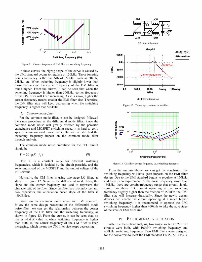
Normally, people use the corner frequency and the slope of the filter to represent the charlatanistic of the filter. For a two-stage differential mode filter, as shown in figure 10, it has two inductors and three capacitors, so the slope of the filter attenuation curve should be -100dB/dec.
Based on the filter attenuation requirement and the attenuation curve of the filter, we are able to get the relationship between the corner-frequency of the filter and the switching frequencies of the converter, as shown in figure 11.
Cx
LDM
Cx
LDM
Cx
(a) Filter Schematic
(b) Filter attenuation
Figure 10. Two-stage differential mode filter
Corner frequency
-100dB/Dec
1484
1 .104 1 .105 1 .106 1 .1071 .104
1 .105
1 .106
fs
20% ripple
30% ripple
40% ripple
Switching frequency (Hz)
Cor
ner f
requ
ency
(Hz)
1 .104 1 .105 1 .106 1 .1071 .104
1 .105
1 .106
fs
20% ripple
30% ripple
40% ripple
Switching frequency (Hz)
Cor
ner f
requ
ency
(Hz)
Figure 11. Corner frequency of DM filter vs. switching frequency
In these curves, the zigzag shape of the curve is caused by the EMI standard begins to regulate at 150kHz. Those jumping points frequency is the one Nth of 150kHz, such as 50kHz, 75kHz, etc. When switching frequency is slightly lower than those frequencies, the corner frequency of the DM filter is much higher. From the curves, it can be seen that when the switching frequency is higher than 500kHz, corner frequency of the DM filter will keep increasing. As it is know, higher the corner frequency means smaller the EMI filter size. Therefore, the DM filter size will keep decreasing when the switching frequency is higher than 500kHz.
b) Common mode filter For the common mode filter, it can be designed followed
the same procedure as the differential mode filter. Since the common mode noise will greatly affected by the parasitic capacitance and MOSFET switching speed, it is hard to get a specific common mode noise value. But we can still find the switching frequency impact on the common mode filter through analysis.
The common mode noise amplitude for the PFC circuit should be
)lg(20 SfKV ⋅= (8)
Here K is a constant value for different switching frequencies, which is decided by the circuit parasitic, and the switching speed of the MOSFET and the output voltage of the PFC circuit.
Normally, the CM filter is using two-stage LC filter, as shown in figure 12. Same as the differential mode filter, the slope and the corner frequency are used to represent the characteristic of the filter. Since the filter has two inductors and two capacitors, the attenuation curve slope of the filter is –80dB/dec.
Based on the common mode noise and EMI standard, follow the same design procedure of the differential mode noise filter, we can get the relationship between the corner frequency of the CM filter and the switching frequency, as shown in figure 13. From the curves, it can be seen that, no matter what K value is, when switching frequency is higher than 400kHz, the corner frequency of the CM filter is keep increasing, which means the CM filter size keeps decreasing.
Cy
Cy
LCM
LCM
Cy
Cy
LCM
LCM
Cy
Cy
LCM
LCM
Cy
Cy
LCM
LCM (a) Filter schematic
(b) Filter attenuation
Figure 12. Two-stage common mode filter
1 .104 1 .105 1 .1061 .104
1 .105
1 .106
f
K=10K=5K=1
Switching frequency (Hz)
Cor
ner f
requ
ency
1 .104 1 .105 1 .1061 .104
1 .105
1 .106
f
K=10K=5K=1
Switching frequency (Hz)
Cor
ner f
requ
ency
Figure 13. CM filter corner frequency vs. switching frequency
From the analysis above, we can get the conclusion: the switching frequency will have great impacts on the EMI filter design. Due to the EMI standard begins to regulate at 150kHz and there is no requirement for the noise frequency lower than 150kHz, there are certain frequency range that circuit should avoid. For those PFC circuit operating at the switching frequency slightly higher than the fraction of 150kHz, the EMI filter size will increase drastically. Since the newly design devices can enable the circuit operating at a much higher switching frequency, it is recommend to operate the PFC switching frequency higher than 400kHz to take the advantage of the smaller EMI filter size.
IV. EXPERIMENTAL VERIFICATION After the theoretical analysis, two single switch CCM PFC
circuits were built, with 100kHz switching frequency and 400kHz switching frequency. Two EMI filters were designed for the converters to meet the EMI standard EN55022 Class B.
Corner frequency
-80dB/Dec
1485

As shown in figure 14, both of the converters can meet the standard at the low frequency range. For the two different EMI filter, we can see that 35% volume reduction is achieved by pushing the switching frequency from 100kHz to 400kHz, which verifies the theoretical analysis. Because the parasitic effects of the EMI filter have the detrimental effects on the EMI filter performance, especially at the high frequency range, it can’t meet the EMI standard at high frequency range. The problem can be solved by using other methods such as grounding and shielding technologies.
0
10
20
30
40
50
60
70
80
100000 1000000 10000000 100000000
Series1standard
f(Hz)
dBuV
0
10
20
30
40
50
60
70
80
100000 1000000 10000000 100000000
Series1standard
0
10
20
30
40
50
60
70
80
100000 1000000 10000000 100000000
Series1standard
f(Hz)
dBuV
(a) 100kHz PFC EMI noise
0
10
20
30
40
50
60
70
80
100000 1000000 10000000 100000000
Series1standard
f(Hz)
dBuV
0
10
20
30
40
50
60
70
80
100000 1000000 10000000 100000000
Series1standard
0
10
20
30
40
50
60
70
80
100000 1000000 10000000 100000000
Series1standard
f(Hz)
dBuV
(b) 400kHz PFC EMI noise
(c) 100kHz PFC EMI filter (d) 400kHz PFC EMI filter
Figure 14. EMI noise after filtering and EMI filter size comparison
V. SWITCHING FREQUENCY IMPACT ON THE BOOST INDUCTOR
Not only the EMI filter, the switching frequency also impacts on the boost inductor of the PFC circuit. It is well known that the boost inductor value will decrease with the increasing of the switching frequency. The higher the switching frequency, the smaller the boot inductor value. As shown the equation 9, the inductor value is reverse proportional to the switching frequency.
ripple
oboost I
Vf
fL22
1)( = (9)
Not only the boost inductor value, the characteristic of the boost inductor also changes with the changing of the switching frequency. As shown in figure 15, the equivalent circuit of the differential mode noise of the PFC circuit, the MOSFET and the diode are represented by a pulse voltage source, because the voltage between MOSFET drain and source is a pulsating voltage. Since the PFC circuit works at the continuous current the mode, there will be two diodes conducting at any time.
Therefore, the diode bridge can be ignored. From the equivalent circuit, it is quite clear that the EMI noise of the circuit will largely affected by the voltage between MOSFET drain and source and the characteristic of the boost inductor.
Load LISN
RLISN
L
RLISN
LZZ
(a) Single switch CCM PFC with LISN (b) EMI equivalent circuit
Figure 15. Equivalent circuit for the EMI modeling
(a) 100kHz Boost inductor (b) 400kHz Boost inductor
Figure 16. Boost inductor for different switching frequencies
0.010.11
101001K
10K100K
1k 10k 100k 1M 10M30MFrequency(Hz)
Impedance (ohm
)
0.010.11
101001K
10K100K
1k 10k 100k 1M 10M30MFrequency(Hz)
Impedance (ohm
)
0.010.11
101001K
10K100K
1k 10k 100k 1M 10M30M0.010.11
101001K
10K100K
1k 10k 100k 1M 10M30MFrequency(Hz)
Impedance (ohm
)
Figure 17. Impedance comparison between two boost inductors for different switching frequencies
There are two boost inductors are designed for a 1kW CCM PFC working at 100kHz and 400kHz respectively, as shown in the figure 16. In figure 17, the impedances of the boost inductors for different switching frequency are shown. It is quite clear that for the boost inductor working at 100kHz, there is a resonant valley at the frequency about 17MHz. At this frequency, the impedance of the boost inductor is small. Therefore, the EMI noise at corresponding frequency is high, which can be seen in figure 18. But for the 400kHz boost inductor, from the impedance curve, we can see that the resonant valley is pushed higher than 30MHz, which means, at the conducted EMI standard required frequency range, there will be not high EMI noise peak as that happens when the switching frequency is 100kHz. The experimental results shows that the PFC circuit operating at 400kHz will not show the high noise peak at high frequency. As it is well known, due to the circuit parasitic, the attenuation of the EMI filter will not keep decreasing with the increasing of the frequency. Normally, the EMI filter attenuation will dramatically decrease
100kHz L
400kHz L
1486

at the high frequency range. Therefore, it is important to eliminate the high frequency noise peak. From the experimental results, we can clear see that the benefit brought by pushing the switching frequency higher.
0
20
40
60
80
100
120
140
160
1.00E+04 1.00E+05 1.00E+06 1.00E+07 1.00E+08Frequency (Hz)
dB(u
V)
0
20
40
60
80
100
120
140
160
1.00E+04 1.00E+05 1.00E+06 1.00E+07 1.00E+08Frequency (Hz)
dB(u
V)
0
20
40
60
80
100
120
140
160
1.00E+04 1.00E+05 1.00E+06 1.00E+07 1.00E+08Frequency (Hz)
dB(u
V)
0
20
40
60
80
100
120
140
160
1.00E+04 1.00E+05 1.00E+06 1.00E+07 1.00E+08Frequency (Hz)
dB(u
V)
Figure 18. EMI noise comparison between tw different switching frequencies
VI. SUMMARY AND CONCLUSION Based on the EMI filter analysis, switching frequency has
pronounced effects on the EMI filter design on the single-switch CCM PFC circuit. When switching frequency is around certain frequency such as 150k, 75k and 50k, etc, the corner frequency of EMI filter will change dramatically. We should keep the switching frequency slightly smaller than these frequencies to get a smaller filter size.
When the switching frequency is higher than a certain value, the filter size will keep decreasing for both the DM and CM filter. Although DM filter size will keep decreasing when the switching frequency is higher than 500kHz, and the CM filter will keep decreasing when the switching frequency is higher than 400kHz, consider the boost inductor size reduction, we should be able to get power density benefit when the
switching frequency is higher than 400kHz, which is verified by the experimental results. Higher switching frequency is preferred for the single-switch CCM PFC.
Not only the EMI filter, but the boost inductor will get the benefit from pushing the switching frequency up, since the inductor is decreasing with the increasing of the switching frequency. At the same time, the smaller inductor value will push the inductor self-resonant frequency up, which will further benefit the circuit EMI performance for the high frequency noise.
REFERENCES
[1] “Adopted specifications of server system infrastructure,” at http://www.ssiforum.org.
[2] Milan M. Jovanovic, Chen Zhou, P. Liao, “Evaluation of active and passive snubber techniques for applications in power factor correction boost converters,” Sixth international conference on Power Semiconductors and their applications (Electronica’92), Munich, Germany, Nov. 11, 1992
[3] Bing Lu, Wei Dong, Qun Zhao, F.C. Lee, “Performance Evaluation of CoolMOSTM and Sic Diode for Single-phase Power Factor Correction Applications,” in Proc. IEEE-APEC 2003’ .
[4] Nave, M.J.,“The effect of duty cycle on SMPS common mode emissions: theory and experiment,” IEEE APEC1989, Page(s): 3 –12
[5] Fu-Yuan Shih; Chen, D.Y.; Yan-Pei Wu; Yie-Tone Chen, “A procedure for designing EMI filters for AC line applications,” Power Electronics, IEEE Transactions on, Volume: 11 Issue: 1, Jan. 1996 Page(s): 170 -181
[6] Ting Guo; Chen, D.Y.; Lee, F.C., “Separation of the common-mode- and differential-mode-conducted EMI noise” Power Electronics, IEEE Transactions on, Volume: 11 Issue: 3, May 1996 Page(s): 480 –488
[7] British Standard “BSEN55022:1998 CISPR 22:1997”
100kHz Noise
400kHz Noise
1487
Copyright © 2022 FDOKUMEN