High-efficiency solution-processed small-molecule solar cells ...
6
High-efficiency solution-processed small- molecule solar cells featuring gold nanoparticles† Abd. Rashid bin Mohd Yusoff, a Seung Joo Lee, a Jin Jang, * a Guankui Long, b Xiangjian Wan b and Yongsheng Chen b The effect of gold nanoparticles embedded in a hole transport layer, poly(3,4-ethylene-dioxythiophene):poly(styrenesulphonate) (PEDOT:PSS), was successfully studied based on small-molecule organic solar cells. The incorporation of nanoparticles results in a power conversion efficiency enhancement of 4.96%. This improve- ment was attributed to enhanced light harvesting because of the localized surface plasmon resonance (LSPR) effect. Solution-processed small-molecule solar cells are attracting attention to be a competing substitute as the most popular investigated organic solar cell. 1 Solution-processed small- molecule solar cells have power conversion efficiency (PCE) higher than 10%. It has been demonstrated to be successful when coordinating chromophores within single molecules and when applied to oligothiophenes with dye units as end caps. 2 Moreover, small molecules are easily synthesized, have high charge carrier mobility, high open-circuit voltage (V OC ), better reproducibility and monodispersity (similarly sized particles), compared to its counterpart, polymer materials. 3–8 In contrast to polymer solar cells, the designing and optimization of the solution-processed small-molecule solar cell is demanding due to the mismatch between optical absorption length and charge transport scale. 9 Therefore, it is imperative to improve light absorption without sacricing the thickness of the active layer. One simple technique to improve light absorption in organic solar cells is the integration of metallic nanoparticles (NPs) to trigger a so-called plasmonic effect. 10 Numerous studies have reported the use of plasmonic organic solar cells with metallic NPs embedded into the (i) hole transport layer (HTL), 11–15 and (ii) active layer. 16–20 Moreover, various types and shapes of metallic NPs have also been used in organic solar cells. 21–25 Although device advancements have demonstrated remarkable improvements in efficiency, there is still limited work on the plasmonic effect of solution-processed small-molecule solar cells. The incorporation of metallic NPs into the HTL, active layer, or ETL, leads to a better hole, electron transports, and improved light absorption. 11–25 Simultaneously, the integration of metallic NPs with various types and shapes is embedded in the active layer, which causes enhancement in the broadband absorption. 14,21–24 In this letter, we study a high-performance, solution- processable small-molecule solar cells with the incorporation of 30 wt% of Au NPs into the poly(3,4-ethylene-dioxythiophene):- poly(styrenesulphonate) (PEDOT:PSS) hole transport layer featuring large band gap, small-molecule DR3TBDTT with a benzo[1,2-b:4,5-b 0 ]dithiophene (BDT) building block (1.74 eV). 25 By incorporating Au NPs into the PEDOT:PSS layer, signicant increases are documented in both J SC and FF, resulting in higher conversion efficiency. Fig. 1a–c show the molecular structure of solution-processed small-molecule DR3TBDTT, the transmission electron micros- copy (TEM) image of Au NPs, and the normalized UV-vis absorption spectrum of Au NPs in chloroform solution, respectively. Au NPs were synthesized using the seed-mediated method. 26,27 Au NPs have an average diameter of about 15 nm with the maximum absorption peak of Au NPs located at 521 nm. In this study, two different small-molecule solar cells were fabricated (Device A: control device without the presence of Au NPs; and B: Au NPs in PEDOT:PSS solution). To conrm the presence of Au NPs in the PEDOT:PSS layer, the atomic force microscopy (AFM) images of the pristine PEDOT:PSS and Au NPs in the PEDOT:PSS layer are shown in Fig. 2. The root-mean-square (RMS) roughness of PEDOT:PSS lms slightly increased from 0.87 to 0.90 nm upon introduction of Au NPs. It can be observed that the RMS roughness is almost constant, and it is noteworthy that Au NPs are safely embedded into the PEDOT:PSS layer without any signicant effect on the surface morphology. a Advanced Display Research Center, Department of Information Display, Kyung Hee University, Dongdaemoon-gu, Seoul 130-701, Korea. E-mail: [email protected] b Key Laboratory of Functional Polymer Materials and The Centre of Nanoscale Science and Technology, Institute of Polymer Chemistry, College of Chemistry, Nankai University, Tianjin 300071, China. E-mail: [email protected] † Electronic supplementary information (ESI) available: Table 1. See DOI: 10.1039/c4ta03536d Cite this: J. Mater. Chem. A, 2014, 2, 19988 Received 10th July 2014 Accepted 6th October 2014 DOI: 10.1039/c4ta03536d www.rsc.org/MaterialsA 19988 | J. Mater. Chem. A, 2014, 2, 19988–19993 This journal is © The Royal Society of Chemistry 2014 Journal of Materials Chemistry A COMMUNICATION Published on 07 October 2014. Downloaded by Nankai University on 18/11/2014 15:48:41. View Article Online View Journal | View Issue
-
Upload
khangminh22 -
Category
Documents
-
view
0 -
download
0
Transcript of High-efficiency solution-processed small-molecule solar cells ...
Journal ofMaterials Chemistry A
COMMUNICATION
Publ
ishe
d on
07
Oct
ober
201
4. D
ownl
oade
d by
Nan
kai U
nive
rsity
on
18/1
1/20
14 1
5:48
:41.
View Article OnlineView Journal | View Issue
High-efficiency s
aAdvanced Display Research Center, Depart
University, Dongdaemoon-gu, Seoul 130-701bKey Laboratory of Functional Polymer Mate
and Technology, Institute of Polymer Ch
University, Tianjin 300071, China. E-mail: y
† Electronic supplementary information10.1039/c4ta03536d
Cite this: J. Mater. Chem. A, 2014, 2,19988
Received 10th July 2014Accepted 6th October 2014
DOI: 10.1039/c4ta03536d
www.rsc.org/MaterialsA
19988 | J. Mater. Chem. A, 2014, 2, 19
olution-processed small-molecule solar cells featuring gold nanoparticles†
Abd. Rashid bin Mohd Yusoff,a Seung Joo Lee,a Jin Jang,*a Guankui Long,b
Xiangjian Wanb and Yongsheng Chenb
The effect of gold nanoparticles embedded in a hole transport
layer, poly(3,4-ethylene-dioxythiophene):poly(styrenesulphonate)
(PEDOT:PSS), was successfully studied based on small-molecule
organic solar cells. The incorporation of nanoparticles results in a
power conversion efficiency enhancement of 4.96%. This improve-
ment was attributed to enhanced light harvesting because of the
localized surface plasmon resonance (LSPR) effect.
Solution-processed small-molecule solar cells are attractingattention to be a competing substitute as the most popularinvestigated organic solar cell.1 Solution-processed small-molecule solar cells have power conversion efficiency (PCE)higher than 10%. It has been demonstrated to be successfulwhen coordinating chromophores within single molecules andwhen applied to oligothiophenes with dye units as end caps.2
Moreover, small molecules are easily synthesized, have highcharge carrier mobility, high open-circuit voltage (VOC), betterreproducibility and monodispersity (similarly sized particles),compared to its counterpart, polymer materials.3–8 In contrast topolymer solar cells, the designing and optimization of thesolution-processed small-molecule solar cell is demanding dueto the mismatch between optical absorption length and chargetransport scale.9 Therefore, it is imperative to improve lightabsorption without sacricing the thickness of the active layer.One simple technique to improve light absorption in organicsolar cells is the integration of metallic nanoparticles (NPs) totrigger a so-called plasmonic effect.10 Numerous studies havereported the use of plasmonic organic solar cells with metallicNPs embedded into the (i) hole transport layer (HTL),11–15 and(ii) active layer.16–20 Moreover, various types and shapes of
ment of Information Display, Kyung Hee
, Korea. E-mail: [email protected]
rials and The Centre of Nanoscale Science
emistry, College of Chemistry, Nankai
(ESI) available: Table 1. See DOI:
988–19993
metallic NPs have also been used in organic solar cells.21–25
Although device advancements have demonstrated remarkableimprovements in efficiency, there is still limited work on theplasmonic effect of solution-processed small-molecule solarcells. The incorporation of metallic NPs into the HTL, activelayer, or ETL, leads to a better hole, electron transports, andimproved light absorption.11–25 Simultaneously, the integrationof metallic NPs with various types and shapes is embedded inthe active layer, which causes enhancement in the broadbandabsorption.14,21–24
In this letter, we study a high-performance, solution-processable small-molecule solar cells with the incorporation of30 wt% of Au NPs into the poly(3,4-ethylene-dioxythiophene):-poly(styrenesulphonate) (PEDOT:PSS) hole transport layerfeaturing large band gap, small-molecule DR3TBDTT with abenzo[1,2-b:4,5-b0]dithiophene (BDT) building block (1.74 eV).25
By incorporating Au NPs into the PEDOT:PSS layer, signicantincreases are documented in both JSC and FF, resulting inhigher conversion efficiency.
Fig. 1a–c show the molecular structure of solution-processedsmall-molecule DR3TBDTT, the transmission electron micros-copy (TEM) image of Au NPs, and the normalized UV-visabsorption spectrum of Au NPs in chloroform solution,respectively. Au NPs were synthesized using the seed-mediatedmethod.26,27 Au NPs have an average diameter of about 15 nmwith the maximum absorption peak of Au NPs located at 521nm. In this study, two different small-molecule solar cells werefabricated (Device A: control device without the presence of AuNPs; and B: Au NPs in PEDOT:PSS solution).
To conrm the presence of Au NPs in the PEDOT:PSS layer,the atomic force microscopy (AFM) images of the pristinePEDOT:PSS and Au NPs in the PEDOT:PSS layer are shown inFig. 2. The root-mean-square (RMS) roughness of PEDOT:PSSlms slightly increased from 0.87 to 0.90 nm upon introductionof Au NPs. It can be observed that the RMS roughness is almostconstant, and it is noteworthy that Au NPs are safely embeddedinto the PEDOT:PSS layer without any signicant effect on thesurface morphology.
This journal is © The Royal Society of Chemistry 2014

Fig. 1 (a) Molecular structures of solution-processed small-moleculeDR3TBDTT, (b) the transmission electron microscopy (TEM) images ofAu NPs, and (c) the normalized UV-vis absorption spectrum of Au NPsin chloroform solution.
Fig. 2 AFM images of (a) PEDOT:PSS and (b) Au NPs:PEDOT:PSSlayers.
Communication Journal of Materials Chemistry A
Publ
ishe
d on
07
Oct
ober
201
4. D
ownl
oade
d by
Nan
kai U
nive
rsity
on
18/1
1/20
14 1
5:48
:41.
View Article Online
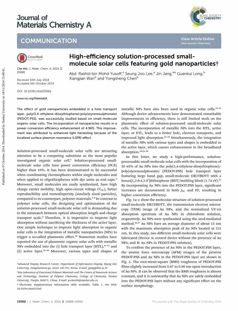
Fig. 3a depicts the current density–voltage (J–V) characteris-tics of the small-molecule solar cells without (red curve) andwith Au NPs (blue curve) embedded into the PEDOT:PSS holetransport layer. The average photovoltaic parameters from tenidentical photovoltaic cells are tabulated in Table 1. In brief, wealso investigated various concentration effects of Au NPs inte-grated into the PEDOT:PSS layer. Their respective J–V charac-teristics are tabulated in Table S1,† which shows the statisticaldata for photovoltaic parameters collected from conventionalsolution-processed small-molecule solar cells under AM1.5sunlight at 100 mW cm�2. The PCE was substantially enhancedfrom 7.58 to 8.92% (from 10 to 40 wt%), resulting mainly fromthe signicant JSC improvement of approximately 4.04%, from13.86 to 14.42 mA cm�2. The FF was also improved, and the VOCwas unchanged, suggesting that the PCE improvement funda-mentally resulted from optical engineering through the inte-grated Au NPs. It is worth noting that the incorporation of suchhigh amounts of NPs in the device could potentially harm theoverall device performance. However, several studies havedemonstrated that the incorporation of high amounts of NPscould still be benecial to the device.28–30
The control device demonstrates an average PCE of 8.66%with an open-circuit voltage (VOC) of 0.92 V, a short-circuitcurrent density (JSC) of 13.29 mA cm�2, and a ll factor (FF) of70.79%. However, upon the integration of Au NPs into thePEDOT:PSS layer, the VOC remained unchanged, while the JSCincreased from 13.29 to 14.50 mA cm�2, and FF decreased from70.79 to 67.93%, leading to an average PCE of 9.06%. Thedecrement of FF can be attributed to the increase in seriesresistance (RS). The RS increases from 2.14 to 2.66 U cm2. On theother hand, JSC improved more (14.50 mA cm�2) than thecontrol device (13.29 mA cm�2).
To nd the origin of the improved JSC because of the opticaleffect of Au NPs, we carried out external quantum efficiency(EQE) measurements. Fig. 3b demonstrates that the
This journal is © The Royal Society of Chemistry 2014
enhancement in the EQE spectra are well matched with theplasmonic resonance region of Au NPs. Integrated JSC from theEQE spectra of the control and plasmonic devices are 12.96 and14.47 mA cm�2, respectively. These values are indeed in agree-ment with the experimental results of JSC of 13.29 and 14.50 mAcm�2, respectively. Please note that throughout this work theerror between the experimental JSC and integrated JSC fromspectral response was less than 4%.31 These values are tabulatedin Table 1 for a clearer comparison, and the slight differencesare a consequence of the spectral mismatch of the xenon lamp,which exhibits a higher photon ux in the UV region than thesun.32
To explain the inuences of Au NPs on exciton generationand dissociation behaviors, we evaluated the maximum excitongeneration rate (Gmax) and exciton dissociation probabilitiesP(E,T) of the control and plasmonic devices. The devices werebiased, sweeping from +1 to�1 V. Fig. 4a shows the dependency
J. Mater. Chem. A, 2014, 2, 19988–19993 | 19989
Fig. 3 (a) J–V characteristics and (b) EQE spectra of control andplasmonic devices.
Journal of Materials Chemistry A Communication
Publ
ishe
d on
07
Oct
ober
201
4. D
ownl
oade
d by
Nan
kai U
nive
rsity
on
18/1
1/20
14 1
5:48
:41.
View Article Online
of the photocurrent density (Jph) on the effective voltage (Veff) forcontrol and plasmonic devices, measured under AM1.5G illu-mination at 100 mW cm�2. Jph is dened as follows:
Jph ¼ JL � JD, (1)
where JL and JD are the current densities under illumination andunder the dark, respectively. Veff is determined as follows:
Veff ¼ V0 � Va, (2)
where V0 is the voltage, when Jph equals 0 (i.e. JL ¼ JD), and Va isthe applied voltage.33
Table 1 Photovoltaic parameters of control and plasmonic devices
Device Jsc (mA cm�2) Jsca (mA cm�2) Voc (V)
Control 13.29 12.96 0.92Plasmonic 14.50 14.27 0.92
a Integrated value from EQE spectra.
19990 | J. Mater. Chem. A, 2014, 2, 19988–19993
Fig. 4a illustrates two distinctive regimes: (i) Jph linearlyincreases at a low Veff, and (ii) Jph saturates at a high Veff, inwhich the internal eld is large enough to dissociate all thephotogenerated excitons into free charge carriers and sweep outall the carriers to the electrodes. Thus, at a high Veff, the satu-ration current density (Jph,sat) is limited by the total number ofabsorbed photons, and assuming that Jph,sat is independent ofbias and temperature, we determined the Gmax as follows:
Jph,sat ¼ qLGmax, (3)
where q is an electronic charge, and L is the thickness of theactive layer.34 The Gmax for the control and the plasmonicdevices are 5.17 � 1027 m�3 s�1 (Jsat ¼ 135 A m�2) and 5.41 �1028 m�3 s�1 (Jsat ¼ 140 A m�2), respectively. The Gmax valuesexhibit considerable improvement aer the integration of AuNPs. It is worth noting that Gmax is the maximum number ofabsorbed photons, and such enhancement corresponds toincreased light absorption in the plasmonic device.
Themechanisms of enhanced light absorption by Au NPs arestudied by the nite-difference time-domain (FDTD) method.35
Fig. 4b shows the distribution of eld intensity around the AuNPs at 680 nm. It is found that the eld intensity increased by afactor of 2 relative to the incident light outside the Au NPs shell,which increases the absorption of the PEDOT:PSS layer. Fig. 4balso illustrates the increase in eld intensity upon incorpo-rating the Au NPs, demonstrating that Au NPs scatter more lightto increase the optical path. Both plasmonic and scatteringeffects excited by the NPs contribute to light absorption insmall-molecule plasmonic solar cells.
For deeper insight into the exciton dissociation probabilities[P(E,T)], Fig. 4c compares the control and plasmonic devices,which are related to the electrical eld (E) and temperature (T).In brief, only a fraction of photogenerated excitons can bedissociated into free carriers. Therefore, the Jph of solar cell canbe written as follows:34,36
Jph ¼ qGmaxP(E,T)L. (4)
The P(E,T) at any bias can be extracted from the curves of thenormalized photocurrent density (Jph/Jsat) with respect to Veff.37
Fig. 4c illustrates the increment of the P(E,T) under short-circuitconditions (Va ¼ 0 V) from 75% for the control device to 90% forthe plasmonic device, implying that the excitation of the LSPRinduced the photogenerated excitons to dissociate into freecarriers. Therefore, it can be concluded that the excitation of theLSPR not only improved the exciton generation rate but also thedissociation probability, thus improving the JSC of the OPVs. To
FF (%) PCE (%) Rs (U cm2) Rsh (U cm2)
70.79 8.66 2.16 93567.93 9.06 2.66 898
This journal is © The Royal Society of Chemistry 2014

Fig. 4 (a) Photocurrent density versus effective voltage, (b) thedistribution of field intensity around the Au NPs at 680 nm, and (c)exciton dissociation probability versus effective voltage for control andplasmonic devices.
Fig. 5 Scattering optical microscopy (NSOM) image for (a) PEDOT:PSSand (b) Au NPs embedded in PEDOT:PSS layer.
Communication Journal of Materials Chemistry A
Publ
ishe
d on
07
Oct
ober
201
4. D
ownl
oade
d by
Nan
kai U
nive
rsity
on
18/1
1/20
14 1
5:48
:41.
View Article Online
further understand the origin of the improvement in theabsorption of Au NPs embedded in a PEDOT:PSS layer, wecarried out near scattering optical microscope (NSOM)measurements38 by evaluating the NSOM signal of thePEDOT:PSS without (Device A) and with Au NP (Device B) layers.The transmission mode with a green laser light (l ¼ 532 nm,
This journal is © The Royal Society of Chemistry 2014
�20 mW) was selected. The incident light passes through eitherPEDOT:PSS or Au NPs:PEDOT:PSS, and the evanescent wave iscaptured by the tip, which is close to the hole transport layer.
Fig. 5a and b show the NSOM images of PEDOT:PSS and AuNPs:PEDOT:PSS, respectively. As shown in Fig. 5b, bright spotswere observed along with a slightly rougher scattering prolecompared to that of the PEDOT:PSS (Fig. 5a). The bright spotscan be attributed to the strong local forward scattering region.39
The RMS values (i.e., the degree of scattering) of the PEDOT:PSSand Au NPs:PEDOT:PSS were 0.52 and 0.75, respectively. Theimprovement is approximately 44.23% for the Au NPs:PE-DOT:PSS layer compared to that of PEDOT:PSS layer. Theseobservations demonstrate that the scattering is furtherimproved by the enhancing plasmonic forward scatteringeffects of the Au NPs.38
Conclusions
In conclusion, we demonstrate that maximum PCE is 9.06%with a relative performance increase of 4.96% in solution-pro-cessed small-molecule solar cells with the integration of Au NPsinto PEDOT:PSS. Absorption spectra, EQE spectra, Gmax, andP(E,T), FDTD simulation, and NSOM conrm that the Au NPsproduced this improvement in the small-molecule solar cells.The enhanced light absorption is the result of both plasmonicand scattering effects by the Au NPs. Enhanced carrier collec-tion and carrier transport properties ensure good performancein plasmonic devices. Therefore, in addition to contributing tolight absorption in the active layer, the Au NPs:PEDOT:PSS layercan facilitate hole collection.
Experimental sectionDevice fabrication
Indium tin oxide (ITO)-coated glass substrates (10 U sq.�1) weresequentially cleaned in detergent, deionized water, acetone andisopropyl alcohol under sonication for 15 min each. Thesubstrates were then dried under a ow of nitrogen and treatedwith UV ozone for 10 min. To prepare a buffer layer, Au NPssolution was doped into PEDOT:PSS (Baytron P 4083). Thediameter of Au NPs is around 15 nm. The PEDOT:PSS solutionswith weight ratios of 10, 20, 30, and 40 wt% Au NPs were spin-
J. Mater. Chem. A, 2014, 2, 19988–19993 | 19991

Journal of Materials Chemistry A Communication
Publ
ishe
d on
07
Oct
ober
201
4. D
ownl
oade
d by
Nan
kai U
nive
rsity
on
18/1
1/20
14 1
5:48
:41.
View Article Online
coated at 5000 rpm for 30 s on ITO substrates and annealed at150 �C in air for 25 min. The thickness of both PEDOT:PSS lmswere around 30 nm, as determined by a surface proler, indi-cating that the incorporation of Au NPs does not change thePEDOT:PSS lm thickness. The optimum weight ratio ofDR3TBDTT with PC71BM was 1 : 0.8 in chloroform, with 0.2 mgmL�1 of polydimethylsiloxane (PDMS) processing additive,which was spin-coated at 1000 rpm for 35 s and later baked at120 �C for 10 min. Finally, 0.5 nm of LiF and 100 nm of Al werethermally evaporated on the active layer under vacuum condi-tion of 1 � 10�7 torr. All devices had an active area of 0.04 cm2,and were encapsulated before any measurements wereperformed.
Device characterization
For small-molecule plasmonic solar cells, the layers comprisingPEDOT:PSS/DR3TBDTT:PC71BM were electrically isolated usingtoluene and methanol along the perimeter, dened by the areaon top of the electrode. This isolation avoids fringing effectsand also prevents overestimation of the photocurrents gener-ated by the device. During the measurements, a shadow mask(0.04 cm2) with a single aperture was placed onto the SM solarcells to dene its photoactive area. The current density–voltage(J–V) characteristics were recorded with a Keithley 2410 sourceunit. The EQE measurements were performed using an EQEsystem (Model 74000) obtained from Newport Oriel Instru-ments USA, and a HAMAMATSU-calibrated silicon cell photo-diode was used as a reference diode. The wavelength wascontrolled with a monochromator of 200–1600 nm. Theabsorption spectrum of Au NPs thin lms was measured using aSCINCO S4100. The surface morphology of the thin lms wasobtained by tapping mode using an atomic force microscope(AFM, Digital Instrument Multimode equipped with a nano-scope IIIa controller). Transmission electron microscopy (TEM)of the Au NPs was performed using a JEOL 1400 TEM with anacceleration voltage of 100 kV. FDTD simulation was performedusing Lumerical Simulation.
Acknowledgements
This work was supported by the MoST (Grant 2014CB643502),NSFC (Grant 51373078), and Human Resources Developmentprogram (no. 20134010200490) of the Korea Institute of EnergyTechnology Evaluation and Planning (KETEP) grant funded bythe Korea government Ministry of Trade, Industry and Energy.
References
1 T. S. van der Poll, J. A. Love, T.-Q. Nguyen and G. C. Bazan,Adv. Mater., 2012, 24, 3646.
2 Y. Liu, C.-C. Chen, Z. Hong, J. Gao, Y. Yang, H. Zhou, L. Dou,G. Li and Y. Yang, Sci. Rep., 2013, 3, 3356.
3 Y. Z. Lin, Y. F. Li and X. W. Zhan, Chem. Soc. Rev., 2012, 41,4245.
4 A. Mishra and P. Bauerle, Angew. Chem., Int. Ed., 2012, 51,2020.
19992 | J. Mater. Chem. A, 2014, 2, 19988–19993
5 B. Walker, C. Kim and T.-Q. Nguyen, Chem. Mater., 2011, 23,470.
6 F. Wurthner and K. Meerholz, Chem.–Eur. J., 2010, 16, 9366.7 Y. Sun, G. C. Welch, W. L. Leong, C. J. Takacs, G. C. Bazanand A. J. Heeger, Nat. Mater., 2012, 11, 44.
8 W. Cambarau, A. Viterisi, J. W. Ryan and E. Palomares, Chem.Commun., 2014, 50, 5349.
9 H. A. Atwater and A. Polman, Nat. Mater., 2010, 9, 205.10 E. Stratakis and E. Kymakis, Mater. Today, 2013, 16, 133.11 S.-J. Ko, H. Choi, W. Lee, T. Kim, B. R. Lee, J.-W. Jung,
J.-R. Jeong, M. H. Song, J. Chul, J. C. Lee, H. Y. Woo andJ. Y. Kim, Energy Environ. Sci., 2013, 6, 1949.
12 E. Stratakis, M. M. Stylianakis, E. Koudoumas andE. Kymakis, Nanoscale, 2013, 5, 4144.
13 M.-K. Chung, S.-W. Lin, F.-C. Chen, C.-W. Chu and C.-S. Hsu,Nanoscale, 2014, 6, 1573.
14 L. Lu, Z. Luo, T. Xu and L. Yu, Nano Lett., 2013, 13, 59.15 J.-L. Wu, F.-C. Chen, Y.-S. Hsiao, F.-C. Chien, P. Chen,
C. H. Kuo, M. H. Huang and C.-S. Hsu, ACS Nano, 2011, 5,959.
16 C.-H. Kim, S.-H. Cha, S. C. Kim, M. Song, J. Lee, W. S. Shin,S.-J. Moon, J. H. Bahng, N. A. Kotov and S.-H. Jin, ACS Nano,2011, 5, 3319.
17 K. Topp, H. Borchert, F. Johnen, A. V. Tunc, M. Knipper,E. von Hauff, J. Parisi and K. Al-Shamery, J. Phys. Chem. A,2010, 114, 3981.
18 D. H. Wang, J. K. Kim, G.-H. Lim, K. H. Park, O. O. Park,B. Lim and J. H. Park, RSC Adv., 2012, 2, 7268.
19 B. Paci, A. Generosi, V. R. Albertini, G. D. Spyropoulos,E. Stratakis and E. Kymakis, Nanoscale, 2012, 4, 7452.
20 D. H. Wang, K. H. Park, J. H. Seo, J. Seifer, J. H. Jeon,J. K. Kim, J. H. Park, O. O. Park and A. J. Heeger, Adv.Energy Mater., 2011, 1, 766.
21 N. N. Lal, B. F. Soares, J. K. Sinha, F. Huang, S. Mahajan,P. N. Bartlett, N. C. Greenham and J. J. Baumberg, Opt.Express, 2011, 19, 11256.
22 D. Qu, F. Liu, Y. Huang, W. Xie and Q. Wu, Opt. Express,2011, 19, 24795.
23 I. Diukman, L. Tzabari, N. Berkovitch, N. Tessler andM. Orenstein, Opt. Express, 2010, 19, A64.
24 S. Xiao and N. A. Mortensen, Opt. Lett., 2011, 36, 37.25 J. Zhou, Y. Zuo, X. Wan, G. Long, Q. Zhang, W. Ni, Y. Liu,
Z. Li, G. He, C. Li, B. Kan, M. Li and Y. Chen, J. Am. Chem.Soc., 2013, 135, 8484.
26 T. Ming, L. Zhao, Z. Yang, H. Chen, L. Sun, J. Wang andC. Yan, Nano Lett., 2009, 9, 3896.
27 X. Xu, A. K. K. Kyaw, B. Peng, D. Zhao, T. K. S. Wong,Q. Xiong, X. W. Sun and A. J. Heeger, Org. Electron., 2013,14, 2360.
28 E. Stratakis, M. M. Stylianakis, E. Koudoumas andE. Kymakis, Nanoscale, 2013, 5, 4144.
29 S.-W. Baek, G. Park, J. Noh, C. Cho, C.-H. Le, M.-K. Seo,H. Song and J.-Y. Lee, ACS Nano, 2014, 8, 3302.
30 C.-H. Kim, S.-H. Cha, S. C. Kim, M. Song, J. Lee, W. S. Shin,S.-J. Moon, J. H. Bahng, N. A. Kotov and S.-H. Jin, ACS Nano,2011, 5, 3319.
This journal is © The Royal Society of Chemistry 2014

Communication Journal of Materials Chemistry A
Publ
ishe
d on
07
Oct
ober
201
4. D
ownl
oade
d by
Nan
kai U
nive
rsity
on
18/1
1/20
14 1
5:48
:41.
View Article Online
31 O. K. Varghese and C. A. Crimes, Sol. Energy Mater. Sol. Cells,2008, 92, 374.
32 A. Duret and M. Gratzel, J. Phys. Chem. B, 2005, 109, 17184.33 S. R. Cowan, A. Roy and A. J. Heeger, Phys. Rev. B: Condens.
Matter Mater. Phys., 2010, 82, 245207.34 V. D. Mihailetchi, H. X. Xie, B. de Boer, L. J. A. Koster and
P. W. M. Blom, Adv. Funct. Mater., 2006, 16, 699.35 Y.-S. Hsiao, C.-P. Chen, C.-H. Chao and W.-T. Whang, Org.
Electron., 2009, 10, 551.
This journal is © The Royal Society of Chemistry 2014
36 V. D. Mihailetchi, L. J. A. Koster, J. C. Hummelen andP. W. M. Blom, Phys. Rev. Lett., 2004, 93, 216601.
37 V. Shrotriya, Y. Yao, G. Li and Y. Yang, Appl. Phys. Lett., 2006,89, 063505.
38 S. W. Baek, J. Noh, C. H. Lee, B. Kim, M. K. Seo and Y. J. Lee,Sci. Rep., 2013, 3, 1726.
39 C. E. Talley, J. B. Jackson, C. Oubre, N. K. Grady,C. W. Hollars, S. M. Lane, T. R. Huser, P. Nordlander andN. J. Halas, Nano Lett., 2005, 5, 1569.
J. Mater. Chem. A, 2014, 2, 19988–19993 | 19993