Fabrication of a Miniaturized ZnO Nanowire Accelerometer ...
Upload
independentCategory
view
0download
0
Top-down Processed SOI Nanowire Devices for Biomedical Applications
S. Ingebrandta, X. T. Vua,b, J.F. Eschermannb, R. Stockmannb, A. Offenhäusserb
a Department of Informatics and Microsystem Technology, University of Applied Sciences Kaiserslautern, 66482 Zweibrücken, Germany
b Institute of Bio- and Nanosystems (IBN), Research Center Jülich, 52425 Jülich, Germany
We present silicon nanowire (SiNW) devices, which were fabricated in a top-down process from silicon-on-insulator (SOI) substrates with a high yield. Electronic characterization proved reliable electronic properties. Here we report the versatile use of the devices in different applications like label-free sensing of DNA hybridization, electronic detection of cellular signals, and detection of proteins. Compared to micro-sized devices, the SiNWs show an improved sensitivity. Analyses of the electronic cell-nanowire contact showed that the important seal resistance is largely increased, which is a prerequisite for highly-sensitive detection of cellular activity. In all applications the SiNW devices show a reliable performance and are highly interesting for future biomedical products.
Introduction Tools with high sensitive and selective detection of chemical and biological substances offer many applications in various fields such as security (1), clinical screening and diagnoses (2-4), drug discovery (5, 6), food control, and environmental monitoring (7, 8). In particular biosensors based on nanoelectronic devices promise a variety of applications in biomedicine for instance for future ‘point-of-care’ diagnostic tools (9-12). In order to miniaturize the tools and to develop cheap and direct electronic ‘hand-held’ devices, most of the time a direct and label-free detection of the analytes is required (13, 14).
In recent years there has been significant progress in the exploration of nanomaterials and nanotechnology for the fabrication of biosensors. The use of silicon nanowires (SiNW) as the sensitive element of such sensor systems was firstly demonstrated by Lieber and coworkers (15). It has been shown that the devices can be very versatile to detect biomolecules such as DNA (14-17), proteins (15), antibodies or antigens (18), bacterial toxins (19), virus (20, 21), cell secretes (22), cardiac markers (23), and electrical activity of cardiac cells (24-26) as well as of neurons (27).
In all related works, different methods for SiNW fabrication are described (14-16, 28-
35). The fabrication processes can be divided into two categories: the “bottom-up” approach that is usually based on the vapor-liquid-solid growth method (VLS) with metal precursers (mostly Au) and the “top-down” approach that is based on advanced lithography techniques. For the “bottom-up” processes most of the time electron beam
ECS Transactions, 35 (7) 3-15 (2011)10.1149/1.3571972 © The Electrochemical Society
3 ) unless CC License in place (see abstract). ecsdl.org/site/terms_use address. Redistribution subject to ECS terms of use (see 54.157.13.203Downloaded on 2016-03-02 to IP

lithography is used to form the metal contacts. In the latter case silicon on insulator (SOI) substrates are predominately used as the starting structure.
In the “bottom-up” approach epitaxial, cylindrical nanowires with a diameter from
several nm to 100 nm are grown with high quality. However, this approach also has several limitations such as complex chip integration, difficulties in individual nanowires positioning and a complicated process to achieve reliable ohmic contacts (33). This results in a low yield of working devices per fabrication process, which leads to immense fabrication costs per device and prevents commercial products so far. In contrast to the “bottom-up” approach, the “top down” approach has several advantages. First of all, the nanowires are uniform in size and well aligned as “process intrinsic” results. The “top-down” methods usually produce functional nanowires in high yields, and in predetermined orientation and position on the substrate (16, 29). In addition the device fabrication can be adapted to industrial CMOS processes, promising a low-cost production of single use test kits.
We present a robust, large scale and reproducible fabrication process for “top-down”
structured SiNW arrays for different biomedical applications. In our approach we combine nanoimprint lithography with anisotropic wet chemical etching in order to produce highly integrated arrays of planar silicon nanowire (SiNW) transistors on 4’’ SOI wafers. Based on this fabrication scheme, we produced planar nanowires having very smooth surfaces and a trapezoid cross section. The smallest dimensions achieved were 70 nm in bottom width and 30 nm in height (typical value was 60 nm), while wires of different length from 3 up to 40 µm were constructed. Two complete fabrication rounds were finalized including top-down structuring, implantation and silicidation of contact lines, passivation of the devices with a stack of oxide and nitride to enable device operation in liquid environments, gate oxide formation, metallization and encapsulation of devices. We fabricated many different designs from 8 channel devices having one common source and individual drain contacts up to highly integrated devices with 128×128 individually addressable nanowires. Different chips were characterized with respect to their electronic behavior. Furthermore, they were utilized to detect electrical signals from living cells in liquid environments or to detect different biomolecules from solution based on specific surface binding.
Materials and Methods Device fabrication
We fabricated two generations of SiNW arrays in a wafer-scale, top-down process
combining nanoimprint lithography and wet chemical etching (16, 17, 35, 36). In the first process we fabricated 16-channel devices with short wires (3-5 µm) having relatively high transconductances and 8-channel devices in a ‘dip-chip’ layout.
The second chip generation was combined with a micro-fluidic system to apply
analyte solutions to the devices. The p-type SiNW biosensor arrays have two lines of 28 individually addressable silicon wires sharing a common source contact. We varied the nanowire designs in lengths (10, 20, or 40 µm) since longer wires were reported to have advantages compared to shorter ones. By tuning the wet etching times we achieved very
ECS Transactions, 35 (7) 3-15 (2011)
4 ) unless CC License in place (see abstract). ecsdl.org/site/terms_use address. Redistribution subject to ECS terms of use (see 54.157.13.203Downloaded on 2016-03-02 to IP

small wires having a bottom width of only 70 nm (with lengths up to 40 µm), while maintaining very smooth surfaces compared to other fabrication methods (34). A detailed description of the first (35) and the second process run (36) was published previously.
For both processes we used an oxide hard mask, which was defined by the
nanoimprint lithography. Then we defined the silicon nanowire structures and the contact lines to the individual wires in one anisotropic wet etching step (Fig. 1).
Figure 1. SiNWs were structured using nanoimprint lithography to define an oxide hard mask under which the silicon was thinned out by anisotropic wet chemical etching. Encapsulation of the devices
For all the measurements presented here, the chips were encapsulated via wire
bonding onto a 68-pin LCC carrier (LCC0850, Spectrum, USA). In order to work in electrolyte solution, a medical epoxy (U300 8OZ, Epo-TEK, USA) was partly filled on the chip to separate the bond wires and bond pads from the electrolyte solution (Fig. 2 A).
Figure 2. Layout of the devices from the second process run. A) Photograph of an encapsulated device. B) Differential interference microscope image of the 2×28 layout of the chip. C) SEM image of three wires having a length of 20 µm and a distance of 50 µm. D) All wires had a trapezoid cross section with a bottom width of 100 nm.
ECS Transactions, 35 (7) 3-15 (2011)
5 ) unless CC License in place (see abstract). ecsdl.org/site/terms_use address. Redistribution subject to ECS terms of use (see 54.157.13.203Downloaded on 2016-03-02 to IP

Chips from the second generation having longer wires (10, 20, or 40 µm) were predominantly used. These chips were fabricated in a 2×28 drain layout sharing a common source contact (Fig 2 B). The two lines of wires were separated by 500 µm whereas the wire-to-wire distance in one line was 50 µm (Fig 2 C). In close-up scanning electron microscope images a nice uniformity with smooth <111> and <100> surfaces of the wires was confirmed (Fig 2 D). Cleaning and surface modification
The devices were cleaned and activated as previously described (36, 37). For
chemical activation, chips were cleaned for 10 min by piranha solution at 60°C and then rinsed with ultrapure water. For the covalent attachment of the probe DNA molecules, a gas phase silanization protocol with 3-glycidoxypropyltrimethoxysilane (GPTMS) was used (37). For the protein experiments a similar gas phase silanization with 3-aminopropyl-triethoxysilane (APTES) was used (37).
The immobilization of the probe DNA was done overnight. The probe DNA
sequences of 20 base-pair (bp) length (5'- amino C6- ATGAACACT-GCATGTAGTCA-3') were incubated with a concentration of 2 µM in a phosphate buffer with 0.5 M NaCl at a basic pH value of 8.5 to optimize the covalent attachment to the GPTMS layer. The hybridization was performed with the perfect match sequence (5' –TGACTA-CATGCAGTGTTCAT- 3') with a concentration of 500 nM for two hours in 1×SSC buffer.
For the cell measurements human embryonic kidney (HEK 293) cells were cultured
as previously described (38-40). The HEK293 cells were grown in minimal essential medium, plus 10% fetal bovine serum, 2 mM glutamine, 1% non-essential amino acids, 100 units/ml penicillin and 100 mg/ml streptomycin (all from Invitrogen, Germany). Cells were cultured for 2-3 days at 37°C and 5% CO2. For image acquisition, cells were fixated and dried before commencing the SEM images and focused ion beam (FIB) preparations (38).
For immobilization of biotin, the SiNW chips were cleaned and modified by gas
phase APTES silanization. We used an EZ-Link Sulfo-NHS-LC-Biotin (sulfosuccinimidyl-6-(biotinamido)hexanoate; Pierce Biotechnology, Inc., USA) with a concentration of 0.5 mg/ml in 10 mM boric acid (pH 8.5). The biotin solution was spotted on the SiNW areas using our micro-spotter followed by incubation for two hours (41). After that the chips were rinsed with ultrapure water in order to remove unbound biotin. This protocol binds the biotin molecules covalently to the silicon oxide surfaces. For biotin-streptavidin binding, the streptavidin was diluted in 0.01×PBS buffer (pH 7) and pipetted to the electrolyte solution during real-time measurement.
Results
In electrical as well as electrochemical characterizations, the nanowires proved correct function in liquid environments (17, 35, 36). For all these measurements we used a leak-free electrochemical reference electrode (Super Dry-Ref (SDR2), WPI, Germany) to apply the gate voltages to the electrolyte enabling a solution-gate operation. The
ECS Transactions, 35 (7) 3-15 (2011)
6 ) unless CC License in place (see abstract). ecsdl.org/site/terms_use address. Redistribution subject to ECS terms of use (see 54.157.13.203Downloaded on 2016-03-02 to IP

backside contact of the silicon substrate below the buried oxide (BOX) was fixed and kept constant in all measurements. The long and thin silicon nanowires behave as ideal long channel field-effect transistor devices. The pH sensitivity was between 40-50 mV/pH, which is a well-known value for silicon oxide surfaces. Electronic detection of DNA hybridization
We previously demonstrated that our SiNW devices are able to detect immobilized
DNA molecules based on their intrinsic charge (42, 43). The chemical shifts were quite large compared to signals that have been presented with ion-sensitive field-effect transistor devices (ISFET) (42, 44). However in these experiments one should take extreme care. First of all the use of a reference electrode in the liquid gate side (front-gate voltage VFG) was mandatory for reliable and reproducible recordings in all of our experiments. Second the electronic signals are very sensitive to side effects. For instance temperature variations or changes in the buffer concentration and pH of the solution should be avoided.
Figure 3. Change of the flat-band voltage of the SiNW chip due to DNA immobilization and hybridization. Due to the negative charge of the DNA, the threshold potential VTH shifts to lower values for the p-type SiNW transistors. The left curves in the inset are the measurements after GPTMS silanization. The central curves and the right curves in the inset are the measurements after probe DNA immobilization and complementary DNA hybridization, respectively.
All electronic measurements of the SiNW transfer characteristics were performed in 0.01×PBS solution at pH 7. After each step an intensive rinsing was performed to wash off any residual solutions from the previous step. The immobilization of DNA reliably resulted in shifts of 100-150 mV in the threshold voltage for many different experiments. In contrast to this, the hybridization signals were always smaller. The DNA hybridization typically resulted in shifts of 20-40 mV, which are about 10 times larger compared to the experiments we published earlier with ISFET devices (42). However, in the previous works we used a different surface chemistry for the devices and maybe the grafting
ECS Transactions, 35 (7) 3-15 (2011)
7 ) unless CC License in place (see abstract). ecsdl.org/site/terms_use address. Redistribution subject to ECS terms of use (see 54.157.13.203Downloaded on 2016-03-02 to IP

density of immobilized DNA was different (45). All the results with SiNW and FET devices are in accordance to the related theoretical models (46-52). Low-noise performance of the silicon nanowires
The main noise contribution to the overall noise of field-effect devices for the
recording of cellular signals is the 1/f noise. This type of noise caused by generation-recombination processes at the silicon/gate oxide interface is predominant in the audio frequency range.
For the extraction of noise spectra, the SiNW devices were connected with a low-
noise amplifier system, which was optimized for the recording of cellular signals with open-gate FETs in previous works (39, 53). To compensate the effects of the much smaller drain-source currents IDS of the SiNWs (about 0.5 µA compared to 0.5 mA for our standard FETs) in the respective working points, we changed the feedback resistor of the first amplification stage from 10 kΩ to 1 MΩ. We exemplarily present here the results for a 40 µm long SiNW of the second process. In the working point of VFG = -1 V and VDS = -2V the wire showed a transconductance of gm = 0.38 µS. As comparison the p-channel transistor with a gate area of Agate = 3×16 μm2 and a gate oxide thickness of 12 nm had a working point of VGS = –1.8 V and VDS = –2.5 V. It revealed a transconductance of gm = 0.5 mS, which is a high value for our standard p-channel devices.
We recorded a noise trace of 5 s from each device. To get clear noise spectra out of
these limited data we used the Wiener-Khintchine theorem (54). First the baseline of the data was corrected using the average value of the noise trace. Then the autocorrelation function was calculated. The autocorrelation-function is a special case of the correlation function for time-dependent noise signal a(t) (a1 = a2 = a). It gives an estimate if the value of a(t1) and the value of a(t1+τ) are correlated. The autocorrelation-function is defined as:
∫+
−∞→
+=+=T
TT
dttataT
tata )()(21lim)()()( τττρ [1]
The absolute value of a Fourier transformed time-event reflects the spectrum of the amplitude of this event. For noise events this time-function is unknown. One can calculate the Fourier transformed autocorrelation-function and receive the noise spectrum.
The Fourier transformed autocorrelation-function w(f) is defined as follows:
∫+∞
∞−
−= ττπτρ diffw )2exp()()( [2]
∫+∞
∞−
= dfiffw )2exp()()( τπτρ [3]
With limitations of the finite noise power and symmetry of the functions, the so-called Wiener-Khintchine Equations are resulting:
ECS Transactions, 35 (7) 3-15 (2011)
8 ) unless CC License in place (see abstract). ecsdl.org/site/terms_use address. Redistribution subject to ECS terms of use (see 54.157.13.203Downloaded on 2016-03-02 to IP

∫+∞
∞−
−= ττπτρ diffW )2exp()(2)( [4]
∫∞
=0
)2cos()()( ττπτρ dffW [5]
These Wiener-Khintchine Equations are valid for all noise functions a(t). The main advantage of this procedure using the autocorrelation function of the same data set is that interspersed noise portions at a certain frequency can be easily identified.
In figure 4 the noise spectra of the two above mentioned devices are directly
compared. It can be seen that both devices exhibit a clear 1/f-noise in the respective frequency range with the SiNW device having a slightly smaller noise power. The noise contribution in our SiNW devices was dependent on the working point of the devices. At lower IDS, which also corresponds to lower gm values close to VFG = 0 V, the smallest noise spectra were measured (55). This is generally well-known from literature and it was previously reported that the sub-threshold regime of SiNW devices has advantages in terms of sensitivity compared to the linear range (56).
Out of the spectra a Hooge’s parameter for the 1/f noise of 0.9 and 0.88 for the FET
and the SiNW device can be extracted, respectively. Both devices have comparable performance in terms of signal-to-noise ratio for extracellular recordings. The noise is most likely governed by the generation-recombination events of defects at the silicon-gate oxide interface. This is quite obvious since we used the same gate oxide (dry oxidation of silicon at 820°C) for both device types.
0,1 1 10 100 10001E-14
1E-13
1E-12
1E-11
1E-10
1E-9
1E-8
2nd generation SiNW FETsFit: 1/f0.88
2nd generation p-channel FETFit: 1/f0.9
1.5E-10 V2/Hz
5E-10 V2/Hz
WFE
T [V2 /H
z]
Frequency [Hz] Figure 4. The noise power spectra of a standard open-gate FET of the second generation used for cell-sensor coupling experiments in our group and of a SiNW of the second generation are compared. The SiNW exhibits a similar performance with a slightly lower noise power in the frequency range relevant for extracellular signals.
ECS Transactions, 35 (7) 3-15 (2011)
9 ) unless CC License in place (see abstract). ecsdl.org/site/terms_use address. Redistribution subject to ECS terms of use (see 54.157.13.203Downloaded on 2016-03-02 to IP
However, the SiNW devices have a main advantage over the standard FET devices. Due to their smaller size it is more likely that the cellular membrane on an individual cell is completely covering the device resulting in very high seal resistances RJ. Since the seal resistance is directly related to the signal amplitude of the extracellular potentials, much higher signal amplitudes and hence better signal-to-noise ratios can be expected. Coupling individual cells to the SiNWs
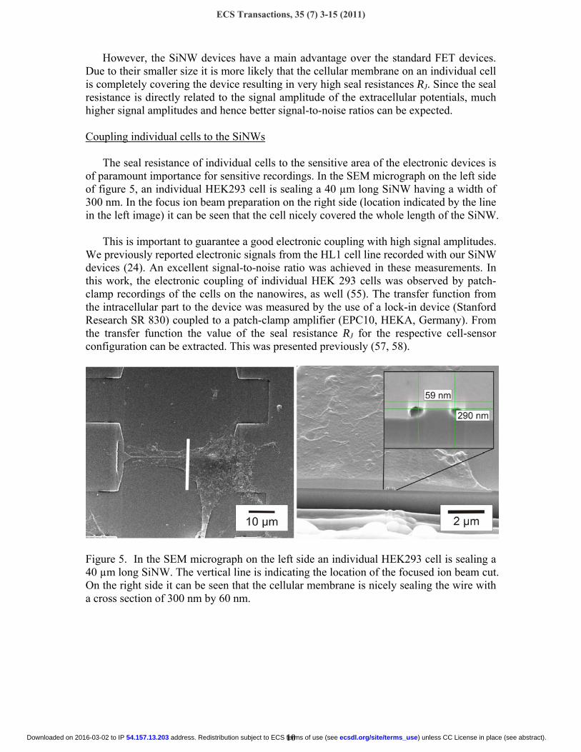
The seal resistance of individual cells to the sensitive area of the electronic devices is
of paramount importance for sensitive recordings. In the SEM micrograph on the left side of figure 5, an individual HEK293 cell is sealing a 40 µm long SiNW having a width of 300 nm. In the focus ion beam preparation on the right side (location indicated by the line in the left image) it can be seen that the cell nicely covered the whole length of the SiNW.
This is important to guarantee a good electronic coupling with high signal amplitudes.
We previously reported electronic signals from the HL1 cell line recorded with our SiNW devices (24). An excellent signal-to-noise ratio was achieved in these measurements. In this work, the electronic coupling of individual HEK 293 cells was observed by patch-clamp recordings of the cells on the nanowires, as well (55). The transfer function from the intracellular part to the device was measured by the use of a lock-in device (Stanford Research SR 830) coupled to a patch-clamp amplifier (EPC10, HEKA, Germany). From the transfer function the value of the seal resistance RJ for the respective cell-sensor configuration can be extracted. This was presented previously (57, 58).
Figure 5. In the SEM micrograph on the left side an individual HEK293 cell is sealing a 40 µm long SiNW. The vertical line is indicating the location of the focused ion beam cut. On the right side it can be seen that the cellular membrane is nicely sealing the wire with a cross section of 300 nm by 60 nm.
ECS Transactions, 35 (7) 3-15 (2011)
10 ) unless CC License in place (see abstract). ecsdl.org/site/terms_use address. Redistribution subject to ECS terms of use (see 54.157.13.203Downloaded on 2016-03-02 to IP

Figure 6. Left: The value of the seal resistance RJ of an individual cell on to of a SiNW device can be extracted by fitting elements of the equivalent circuit on the left to the measured transfer functions. Multiple measurements with SiNW chips from the first and the second generation clearly showed that the membrane seal for the longer wires from the second process was better. In figure 6 the equivalent electronic circuit for the extraction of the seal resistances is shown. The transfer function
P
J
VVH =)(ω [6]
between the pipette voltage VP and the voltage in the junction VJ is measured. In these experiments the transfer functions of the patch-clamp amplifier and rest of the setup were taken into account (55) and corrected accordingly.
As a result from the FIB preparations and from the electronic coupling measurements it was clearly elaborated that the seal resistance and hence the electronic coupling of the cellular membrane was better for the second generation devices compared to the first generation devices. Main difference between the designs was the length of the wires (3 µm for the first and 10, 20, or 40 µm for the second process). In the first generation also 6 wires in parallel were fabricated (24, 35), which revealed the worst coupling values compared to the other designs. Electronic detection of proteins
As a third example, the fully-electronic detection of protein binding is presented. We
monitored the binding event of biotin-streptavidin, which is known as the strongest non-covalent biomolecular interaction in nature. Steptavidin has four binding sites for biotin. This property is used for targeted molecules in many different biomoleculer detection technologies such as ELISA. In related literature, the biotin-streptavidin complex is typically employed to boost the sensitivity of devices and also to understand the mechanisms of the detection schemes.
ECS Transactions, 35 (7) 3-15 (2011)
11 ) unless CC License in place (see abstract). ecsdl.org/site/terms_use address. Redistribution subject to ECS terms of use (see 54.157.13.203Downloaded on 2016-03-02 to IP

Figure 7. Left: Electronic, real-time detection of biotin-streptavidin binding. The largest effects were visible at a concentration of 2.5 µg/ml. This is in accordance to the flat-band voltage shift of 18 mV measured in the transfer characteristics of this chip (right).
In our experiments the electronic characterizations of the SiNWs was carried out in
0.01×PBS buffer at pH 7. In this pH regime the streptavidin molecules are negatively and the biotin molecules are positively charged. The binding of streptavidin to biotin can be followed in a real-time recording due to the large binding affinity of the molecules. The SiNW chips were set to a working point in saturation regime and the current was recorded. In figure 7 the concentration dependent current change is shown, when streptavidin was introduced to the electrolyte. The measurement started with pure 0.01×PBS buffer. Then streptavidin was added to achieve a concentration of 0.25 μg/ml. The concentration was increased step-wisely up to a concentration of 10 µg/ml. The largest visible effect was at the streptavidin concentration of 2.5 µg/ml. This real-time measurement was confirmed also with transfer characteristic measurements after rinsing the chip with buffer solution. The flat-band voltage shift was 18 mV in accordance to the real-time measurements.
Conclusions We successfully fabricated in a large-scale approach arrays of silicon nanowire
transistors. The devices proved good electronic performance. First label-free detection experiments with DNA and proteins were successful. Compared to our standard open-gate FET devices the SiNWs are similar in their 1/f-noise characteristics. However, with the SiNW devices much higher seal resistances of the cellular membrane with the devices can be achieved, which should result in higher signal amplitudes in extracellular recordings. In future we will use these devices for clinically relevant biomedical experiments and for the detection of electronic signals from electrogenic cells.
Acknowledgments
The fabrication of the nanowire devices was done in the clean room facilities of the Institute of Bio- and Nanosystems (IBN) at the Research Center Jülich (FZJ). Financial support during that time came from the German Research Foundation through the project ‘‘Biointerface-GRK 1035’’ and from the Helmholtz association. We thank K. H. Deusen,
ECS Transactions, 35 (7) 3-15 (2011)
12 ) unless CC License in place (see abstract). ecsdl.org/site/terms_use address. Redistribution subject to ECS terms of use (see 54.157.13.203Downloaded on 2016-03-02 to IP

W. Michelsen, and H. P. Bochem for LPCVD deposition, ion implantation, and SEM measurements, respectively. We thank Daniela Esser for the FIB preparation and measurements. We also thank N. Wolters, R. Otto, and D. Strobl for the design, development and fabrication several low-noise amplifier systems and D. Lomparski for implementation of the readout software.
Current financial support for X.T.V. comes from the BMBF/AIF
IngenieursNachwuchsFH project 'Multifunktionales Pharmascreening mit Cell-Chip Hybridsystemen' (17N2110).
References
1 D. V. Lim, J. M. Simpson, E. A. Kearns and M. F. Kramer, Clin. Microbiol. Rev., 18, 583 (2005).
2 D. C. Hay Burgess, J. Wasserman and C. A. Dahl, Nature, (2006). 3 F. S. Ligler and J. S. Erickson, Nature, 440, 159 (2006). 4 P. D'Orazio, Clin. Chim. Acta, 334, 41 (2003). 5 M. A. Cooper, Curr. Opin. Pharmacol., 3, 557 (2003). 6 M. A. Cooper, Nat. Rev. Drug Discov., 1, 515 (2002). 7 E. C. Alocilja and S. M. Radke, Biosens. Bioelectron., 18, 841 (2003). 8 D. Ivnitski, I. Abdel-Hamid, P. Atanasov and E. Wilkins, Biosens. Bioelectron.,
14, 599 (1999). 9 J. S. Daniels and N. Pourmand, Electroanalysis, 19, 1239 (2007). 10 J. Wang, Biosens. Bioelectron., 21, 1887 (2006). 11 J. Albers, T. Grunwald, E. Nebling, G. Piechotta and R. Hintsche, Anal. Bioanal.
Chem., 377, 521 (2003). 12 E. Stürenburg and R. Junker, Dtsch Arztebl Int, 106, 48 (2008). 13 S. A. Soper, K. Brown, A. Ellington, B. Frazier, G. Garcia-Manero, V. Gau, S. I.
Gutman, D. F. Hayes, B. Korte, J. L. Landers, D. Larson, F. Ligler, A. Majumdar, M. Mascini, D. Nolte, Z. Rosenzweig, J. Wang and D. Wilson, Biosens. Bioelectron., 21, 1932 (2006).
14 Z. Q. Gao, A. Agarwal, A. D. Trigg, N. Singh, C. Fang, C. H. Tung, Y. Fan, K. D. Buddharaju and J. M. Kong, Anal. Chem., 79, 3291 (2007).
15 Y. Cui, Q. Q. Wei, H. K. Park and C. M. Lieber, Science, 293, 1289 (2001). 16 E. Stern, J. F. Klemic, D. A. Routenberg, P. N. Wyrembak, D. B. Turner-Evans,
A. D. Hamilton, D. A. LaVan, T. M. Fahmy and M. A. Reed, Nature, 445, 519 (2007).
17 X. T. Vu, R. GhoshMoulick, J. F. Eschermann, R. Stockmann, A. Offenhausser and S. Ingebrandt, Sens. Actuator B-Chem., 144, 354 (2010).
18 A. Kim, C. S. Ah, H. Y. Yu, J. H. Yang, I. B. Baek, C. G. Ahn, C. W. Park, M. S. Jun and S. Lee, Appl. Phys. Lett., 91, (2007).
19 N. N. Mishra, W. C. Maki, E. Cameron, R. Nelson, P. Winterrowd, S. K. Rastogi, B. Filanoski and G. K. Maki, Lab Chip, 8, 868 (2008).
20 F. Patolsky, G. Zheng and C. M. Lieber, Nanomedicine, 1, 51 (2006). 21 F. Patolsky, G. Zheng, O. Hayden, M. Lakadamyali, X. Zhuang and C. M. Lieber,
101, 14017 (2004). 22 T. S. Pui, A. Agarwal, F. Ye, Z. Q. Ton, Y. X. Huang and P. Chen, Nanoscale, 1,
159 (2009).
ECS Transactions, 35 (7) 3-15 (2011)
13 ) unless CC License in place (see abstract). ecsdl.org/site/terms_use address. Redistribution subject to ECS terms of use (see 54.157.13.203Downloaded on 2016-03-02 to IP

23 J. H. Chua, R. E. Chee, A. Agarwal, S. M. Wong and G. J. Zhang, Anal. Chem., 81, 6266 (2009).
24 J. F. Eschermann, R. Stockmann, M. Hueske, X. T. Vu, S. Ingebrandt and A. Offenhausser, Appl. Phys. Lett., 95, (2009).
25 T. Cohen-Karni, Q. Qing, Q. Li, Y. Fang and C. M. Lieber, Nano Lett., 10, 1098 (2010).
26 T. Cohen-Karni, B. P. Timko, L. E. Weiss and C. M. Lieber, Proc. Natl. Acad. Sci. U. S. A., 106, 7309 (2009).
27 F. Patolsky, B. P. Timko, G. Yu, Y. Fang, A. B. Greytak, G. Zheng and C. M. Lieber, 313, 1100 (2006).
28 N. Elfstrom, A. E. Karlstrom and J. Linnrost, Nano Lett., 8, 945 (2008). 29 A. Agarwal, K. Buddharaju, I. K. Lao, N. Singh, N. Balasubramanian and D. L.
Kwong, Sens. Actuator A-Phys., 145, 207 (2008). 30 O. H. Elibol, D. Morisette, D. Akin, J. P. Denton and R. Bashir, 83, 4613 (2003). 31 Z. Li, Y. Chen, X. Li, T. I. Kamins, K. Nauka and R. S. Williams, Nano Lett., 4,
245 (2004). 32 N. A. Melosh, A. Boukai, F. Diana, B. Gerardot, A. Badolato, P. M. Petroff and J.
R. Heath, Science, 300, 112 (2003). 33 F. Patolsky, G. Zheng and C. M. Lieber, 1, 1711 (2006). 34 H. D. Tong, S. Chen, W. G. van der Wiel, E. T. Carlen and A. van den Berg,
(2009). 35 X. T. Vu, J. F. Eschermann, R. Stockmann, R. GhoshMoulick, A. Offenhausser
and S. Ingebrandt, Phys. Status Solidi A-Appl. Mat., 206, 426 (2009). 36 X. T. Vu, R. Stockmann, B. Wolfrum, A. Offenhaesser and S. Ingebrandt, Phys.
Status Solidi A-Appl. Mat., 207, 850 (2010). 37 R. GhoshMoulick, X. T. Vu, S. Gilles, D. Mayer, A. Offenhausser and S.
Ingebrandt, Phys. Status Solidi A-Appl. Mat., 206, 417 (2009). 38 G. Wrobel, M. Hoeller, E. Sommerhage, M. Schindler, S. Ingebrandt and A.
Offenhaeusser, 34, 716 (2005). 39 G. Wrobel, R. Seifert, S. Ingebrandt, J. Enderlein, H. Ecken, A. Baumann, U. B.
Kaupp and A. Offenhausser, 89, 3628 (2005). 40 F. Sommerhage, R. Helpenstein, A. Rauf, G. Wrobel, A. Offenhausser and S.
Ingebrandt, Biomaterials, 29, 3927 (2008). 41 S. Ingebrandt and A. Offenhäusser, Phys. Status Solidi A-Appl. Mat., 203, 3399
(2006). 42 F. Uslu, S. Ingebrandt, D. Mayer, S. Bocker-Meffert, M. Odenthal and A.
Offenhausser, 19, 1723 (2004). 43 J. Fritz, E. B. Cooper, S. Gaudet, P. K. Sorger and S. R. Manalis, Proc. Natl. Acad.
Sci. U. S. A., 99, 14142 (2002). 44 S. Ingebrandt and A. Offenhausser, 203, 3399 (2006). 45 J. P. Cloarec, J. R. Martin, C. Polychronakos, I. Lawrence, M. F. Lawrence and E.
Souteyrand, Sens. Actuator B-Chem., 58, 394 (1999). 46 Y. Liu and R. W. Dutton, J. Appl. Phys., 106, (2009). 47 W. R. McKinnon, D. Landheer and G. Aers, J. Appl. Phys., 104, (2008). 48 D. Landheer, W. R. McKinnon, W. H. Jiang and G. Aers, Appl. Phys. Lett., 92,
(2008). 49 D. Landheer, W. R. McKinnon, G. Aers, W. Jiang, M. J. Deen and M. W.
Shinwari, IEEE Sens. J., 7, 1233 (2007). 50 B. K. Wunderlich, P. A. Neff and A. R. Bausch, Appl. Phys. Lett., 91, (2007).
ECS Transactions, 35 (7) 3-15 (2011)
14 ) unless CC License in place (see abstract). ecsdl.org/site/terms_use address. Redistribution subject to ECS terms of use (see 54.157.13.203Downloaded on 2016-03-02 to IP

51 W. R. McKinnon and D. Landheer, J. Appl. Phys., 100, (2006). 52 A. Poghossian, A. Cherstvy, S. Ingebrandt, A. Offenhäusser and M. J. Schöning,
Sens. Actuator B-Chem., 111, 470 (2005). 53 A. Offenhausser, C. Sprossler, M. Matsuzawa and W. Knoll, Biosens.
Bioelectron., 12, 819 (1997). 54 R. Müller, Rauschen, Springer Verlag, Berlin, Germany (1990). 55 J. F. Eschermann, Silicium Nanodrähte für die extrazelluläre Ableitung
elektrischer Aktivität, Dissertation, Department for Electrotechnique and Information Technology, RWTH Aachen University, Aachen, Germany, (2010).
56 X. P. A. Gao, G. F. Zheng and C. M. Lieber, Nano Lett., 10, 547 (2010). 57 P. Fromherz, C. O. Muller and R. Weis, Phys. Rev. Lett., 71, 4079 (1993). 58 R. Weis and P. Fromherz, Phys. Rev. E, 55, 877 (1997).
ECS Transactions, 35 (7) 3-15 (2011)
15 ) unless CC License in place (see abstract). ecsdl.org/site/terms_use address. Redistribution subject to ECS terms of use (see 54.157.13.203Downloaded on 2016-03-02 to IP
Copyright © 2022 FDOKUMEN