Analysis of photovoltaic cell parameters of non-vacuum solution processed Cu(In, Ga)Se2 thin film...
10
Analysis of photovoltaic cell parameters of non-vacuum solution processed Cu(In, Ga)Se 2 thin film based solar cells Firoz Khan, Hyun-Jung Lee, Misol Oh, Jae Hyun Kim ⇑ Energy Research Division, Daegu Gyeongbuk Institute of Science & Technology (DGIST), 50-1 Sang-Ri, Hyeonpung-Myeon, Dalseong-gun, Daegu 711-873, Republic of Korea Received 25 April 2014; received in revised form 29 June 2014; accepted 30 June 2014 Communicated by: Associate Editor Nicola Romeo Abstract The losses in Cu(In, Ga)Se 2 (CIGS) solar cells due to photovoltaic (PV) cell parameters, namely the shunt resistance R sh , series resis- tance R s , diode ideality factor n, and reverse saturation current density J 0 , were analyzed in this study. The PV cell parameters of the solar cells were analytically determined for various doping concentrations of Cu and In in CIGS films. The CIGS films were deposited using a low cost non-toxic solvent (deionized) by a non-vacuum process (spray pyrolysis technique). They were subsequently character- ized using XRD, FE-SEM, I–V and UV–Vis techniques to correlate the structural, electrical, and optical properties of the films with solar cell performance. Maximum short circuit current density of 0.0218 A/cm 2 is achieved for Cu/Se and In/Se molar ratios of 0.131 and 0.318, respectively. However, the maximum obtained V oc value is 0.431 V for Cu/Se and In/Se molar ratios of 0.105 and 0.191, respec- tively. The maximum achieved efficiency was 4.38% for Cu/Se and In/Se molar ratios of 0.105 and 0.191, respectively. Analytically predicted values of R sh , R s , n, and J 0 were 116.82 X cm 2 , 4.64 X cm 2 , 1.8016, and 1.4952 10 6 A/cm 2 , respectively. Ó 2014 Elsevier Ltd. All rights reserved. Keywords: Thin film solar cell; Cu(In, Ga)Se 2 (CIGS); Non-vacuum process; Photovoltaic cell parameters 1. Introduction Solar energy is unlimited, free, and not localized to any part of the world, and on this basis photovoltaic (PV) is recognized as one of the most promising sustainable energy technologies. It simultaneously helps to meet energy demand and address environmental problems. Every minute the sun provides the earth with enough solar energy to meet its power needs for a year (Khan, 2011). Through PV technology solar energy can be converted to electrical energy directly by solar cells without emission of green- house gases. Generally, solar cells for terrestrial application are made from inorganic semiconductor materials, e.g. silicon (Si), gallium arsenide (GaAs), and Cu(In, Ga)Se 2 (CIGS), which absorb a very large percentage of solar radiation and convert it into electricity. Among the materials generally used to fabricate solar cells, CIGS is the most promising candidate due to its tun- able direct band gap (1.0–2.4 eV) and high absorption coef- ficient (a 10 5 cm 1 )(Cho et al., 2013). If the a values of a semiconductor are more than 10 4 cm 1 , then cell thickness of less than 3 lm is required to absorb up to 95% of the useful incident solar radiation. On the other hand, single crystal silicon with a a value < 10 3 cm 1 for the 900 to 1150 nm range of the solar spectrum requires cell thickness exceeding 300 lm to absorb 95% of the useful AM1.5G solar radiation (in 290 < k < 1150 nm range) incident on solar cell (Khan, 2011). http://dx.doi.org/10.1016/j.solener.2014.06.038 0038-092X/Ó 2014 Elsevier Ltd. All rights reserved. ⇑ Corresponding author. Tel.: +82 53 7853610; fax: +82 53 7853439. E-mail address: [email protected] (J.H. Kim). www.elsevier.com/locate/solener Available online at www.sciencedirect.com ScienceDirect Solar Energy 108 (2014) 189–198
Transcript of Analysis of photovoltaic cell parameters of non-vacuum solution processed Cu(In, Ga)Se2 thin film...
Available online at www.sciencedirect.com
www.elsevier.com/locate/solener
ScienceDirect
Solar Energy 108 (2014) 189–198
Analysis of photovoltaic cell parameters of non-vacuumsolution processed Cu(In, Ga)Se2 thin film based solar cells
Firoz Khan, Hyun-Jung Lee, Misol Oh, Jae Hyun Kim ⇑
Energy Research Division, Daegu Gyeongbuk Institute of Science & Technology (DGIST), 50-1 Sang-Ri, Hyeonpung-Myeon, Dalseong-gun,
Daegu 711-873, Republic of Korea
Received 25 April 2014; received in revised form 29 June 2014; accepted 30 June 2014
Communicated by: Associate Editor Nicola Romeo
Abstract
The losses in Cu(In, Ga)Se2 (CIGS) solar cells due to photovoltaic (PV) cell parameters, namely the shunt resistance Rsh, series resis-tance Rs, diode ideality factor n, and reverse saturation current density J0, were analyzed in this study. The PV cell parameters of thesolar cells were analytically determined for various doping concentrations of Cu and In in CIGS films. The CIGS films were depositedusing a low cost non-toxic solvent (deionized) by a non-vacuum process (spray pyrolysis technique). They were subsequently character-ized using XRD, FE-SEM, I–V and UV–Vis techniques to correlate the structural, electrical, and optical properties of the films with solarcell performance. Maximum short circuit current density of 0.0218 A/cm2 is achieved for Cu/Se and In/Se molar ratios of 0.131 and0.318, respectively. However, the maximum obtained Voc value is 0.431 V for Cu/Se and In/Se molar ratios of 0.105 and 0.191, respec-tively. The maximum achieved efficiency was �4.38% for Cu/Se and In/Se molar ratios of 0.105 and 0.191, respectively. Analyticallypredicted values of Rsh, Rs, n, and J0 were 116.82 X cm2, 4.64 X cm2, 1.8016, and 1.4952 � 10�6 A/cm2, respectively.� 2014 Elsevier Ltd. All rights reserved.
Keywords: Thin film solar cell; Cu(In, Ga)Se2 (CIGS); Non-vacuum process; Photovoltaic cell parameters
1. Introduction
Solar energy is unlimited, free, and not localized to anypart of the world, and on this basis photovoltaic (PV) isrecognized as one of the most promising sustainable energytechnologies. It simultaneously helps to meet energydemand and address environmental problems. Everyminute the sun provides the earth with enough solar energyto meet its power needs for a year (Khan, 2011). ThroughPV technology solar energy can be converted to electricalenergy directly by solar cells without emission of green-house gases. Generally, solar cells for terrestrial application
http://dx.doi.org/10.1016/j.solener.2014.06.038
0038-092X/� 2014 Elsevier Ltd. All rights reserved.
⇑ Corresponding author. Tel.: +82 53 7853610; fax: +82 53 7853439.E-mail address: [email protected] (J.H. Kim).
are made from inorganic semiconductor materials, e.g.silicon (Si), gallium arsenide (GaAs), and Cu(In, Ga)Se2
(CIGS), which absorb a very large percentage of solarradiation and convert it into electricity.
Among the materials generally used to fabricate solarcells, CIGS is the most promising candidate due to its tun-able direct band gap (1.0–2.4 eV) and high absorption coef-ficient (a � 105 cm�1) (Cho et al., 2013). If the a values of asemiconductor are more than 104 cm�1, then cell thicknessof less than 3 lm is required to absorb up to 95% of theuseful incident solar radiation. On the other hand, singlecrystal silicon with a a value < 103 cm�1 for the 900 to1150 nm range of the solar spectrum requires cell thicknessexceeding 300 lm to absorb �95% of the useful AM1.5Gsolar radiation (in 290 < k < 1150 nm range) incident onsolar cell (Khan, 2011).

190 F. Khan et al. / Solar Energy 108 (2014) 189–198
CIGS thin film solar cells, wherein a thin layer ofphotovoltaic material is deposited on thick or thin flexiblesubstrates, are fabricated with a thickness of 1–3 lm due totheir high a values. A junction is formed at or near theCdS–CIGS (n–p) interface using p-type CIGS and n-typeCdS and ZnO materials. The charge carriers that are gen-erated within the junction-field region or within one diffu-sion length in the solar cell are collected. Generally, thefront and back contacts are made with Al (low work func-tion) and Mo (high work function), respectively. In thistechnology a relatively small amount of raw materials isrequired, thus making it attractive for producing low costsolar cells. However, the deposition of photovoltaic mate-rials onto large areas is one of the key challenges presentlyfacing the thin film industry (Malsch, 2003). The majordrawback of thin film technology is that the efficiencyand the lifetime of thin film solar cells are respectivelylow compared to wafer based silicon solar cell technology.Despite these drawbacks, the low cost and the capability ofdeposition on flexible substrates make thin film solar cellsattractive compared with wafer based silicon solar cells.To date, the maximum reported CIGS solar cell efficiencyat the laboratory level is �20% with of aperture area of0.50 cm2 (Jackson et al., 2011). Due to the requirementof vacuum processing, however, this technology is not costeffective. Notably, several researchers (Ahn et al., 2010;Cho et al., 2013; Guo et al., 2008; Kim and Kim, 2012;Liu et al., 2010; Mitzi et al., 2008; Schulz et al., 1998) havefabricated CIGS solar cells using non-vacuum technology.Most of these groups used a toxic chemical as a solvent fordeposition of the CIGS film (Cho et al., 2013; Mitzi et al.,2008; Liu et al., 2010). Cho et al. (2013) recently achieved4.19% efficiency with a CuISe2 (CIS) thin film solar cellusing a hybrid ink in which a toxic solvent (methanol) isused to deposit the CIS film. However, Ho et al. (2014)have deposited CuIn(S, Se)2 thin film using the non-toxicsolvent (deionized water) by spray pyrolysis technique.
The performance of a PV cell is represented by the per-formance parameters, namely, the short circuit currentdensity Jsc, open circuit voltage Voc, curve factor CF, andefficiency g of the cell. These parameters strongly dependupon the PV cell parameters (shunt resistance Rsh, seriesresistance Rs, diode ideality factor n, and reverse saturationcurrent density J0) of the solar cells (Khan et al., 2011). ThePV cell parameters are indicative of the losses in the solarcells. In the case of CIGS solar cells, the performancestrongly depends upon the doping concentration of copper(Cu) and indium (In). It is thus important to investigate thedependency of the performance of CIGS solar cells on Cuand In content to achieve maximal efficiency.
In this study, we investigated the dependency of PV cellsand the performance parameters of non-vacuum processedCIGS thin film based solar cells on the doping concentra-tion of Cu and In with the aim of maximizing the solar cellperformance by reducing the combined loss due to Rsh, Rs,n, and J0. We have used a non-toxic solvent (deionized
water) to deposit the CIGS thin films using spray pyrolysistechnique (Ho et al., 2014).
1.1. Theoretical
The steady state J–V characteristics of a p–n junctionsilicon solar cell are often described based on single diodemodel for the J–V curve in the IVth quadrant, given as(Khan et al., 2011).
J ¼ �J ph þ J 0 eðV�JRsÞ
nV T � 1� �
þ ðV � JRsÞRsh
ð1Þ
where VT = kT/q, Jph = light generated current density,q = electronic charge, k = Boltzmann’s constant, andT = operating temperature of the solar cell.
Eq. (1) can be used to derive the relations to extract thePV cell parameters of a solar cell, as given below (Khanet al., 2010a).
Rsh ¼1
mscð2Þ
1
moc¼ Rs þ nV T �
1
ðJ sc � mscV ocÞð3Þ
1
moc¼ Rs þ
nV T
J 0
� e�V ocnV T
� �ð4Þ
where msc and moc are the slopes (dI/dV) at short (V = 0,J = �Jsc) and open circuit (V = Voc, J = 0). The value ofRsh can be determined directly using the value of msc fromEq. (2). The values of Rs and n can be respectively deter-mined from the intercept and the slope of a plot betweenmoc�1 vs. (Jsc � mscVoc)
�1 at various intensities of illumina-tion. The value of J0 can be determined from the slope ofthe plot of moc
�1 vs. exp (�Voc/nVT) using Eq. (4). Combi-nation of Eqs. (2)–(4) can be used to extract the values ofPV cell parameters of a solar cell.
2. Experimental
2.1. Reagents
Cupper (II) chloride (CuCl2, 99.999%, Sigma Aldrich),indium (III) chloride (InCl3, 99.999%, Sigma Aldrich), gallium(III) chloride (GaCl3, 99.999%, Sigma Aldrich), selenourea(NH2CSeNH2, 99.98%, Alfa Aesar), elemental seleniumpowder (Se, 99.99%, 5 N Plus Inc.), cadmium sulfate(CdSO4, 99.99, Sigma Aldrich), thiourea (NH2CSeNH2,99.0%, Sigma Aldrich), ammonium hydroxide solution(NH4OH, 99.99%, Sigma Aldrich), and deionized water(DIW, with resistivity of 18.2 MX) were used as reagentsfor the Cu(In, Ga)Se2 solar cells fabrication.
2.2. Synthesis of CIGS films
An aqueous solution of the CIGS precursor was pre-pared by dissolving a mixture of copper (II) chloride,
F. Khan et al. / Solar Energy 108 (2014) 189–198 191
indium (III) chloride, gallium (III) chloride, and selenoureain DIW. A homogeneous solution was prepared using amagnetic stirrer at room temperature. In this study, twotypes (A and B) of solutions were prepared. In both typesof solutions, the concentrations of gallium (III) chlorideand selenourea were kept constant at 0.0021 and0.0711 M, respectively. In the A type solutions, the concen-tration of cupper (II) chloride was varied as 0.0056, 0.0074,and 0.0093 M, whereas the concentration of indium (III)chloride was constant at 0.0226 M. In the B type solutions,the concentration of indium (III) chloride was varied as0.0057, 0.0136, and 0.0226 M and the concentration ofcupper (II) chloride was constant (0.0074 M).
Prior to CIGS film deposition, molybdenum (Mo)coated glass substrates were thoroughly cleaned in acetone.The cleaned substrates were preheated at 300 �C for 10 minusing a hot plate. The films were deposited using the spraypyrolysis technique. Pure nitrogen gas was used as a carriergas with a flow rate of 3.51 l/min for 20 min. Separation of30 cm between the substrate and the nozzle was maintainedduring the film deposition.
2.3. Solar cell fabrication
The CIGS thin film coated samples underwent a seleni-zation process using the molecular beam epitaxy (MBE)technique. Se powder was used as a Se vapor source foreffusion. The temperature profile and the Se effusion ratefor the selenization process are shown in Fig. 1. Afterselenization, a cadmium sulfite (CdS) buffer layer withthickness of �50 nm was deposited for junction formationvia chemical bath deposition. Cadmium sulfate (0.002 M),thiourea (0.02 M), and ammonium hydroxide were used forCdS deposition at 60 �C for 10 min. Zinc oxide (ZnO) andindium tin oxide (ITO) window layers with thickness of�60 and �350 nm, respectively, were deposited using DCsputtering. Finally, a front contact of nickel (�50 nm)and silver (�1000 nm) was realized using e-beam evapora-tion technique.
Fig. 1. A typical temperature profile along with Se effusion rate of theselenization process.
2.4. Characterization techniques
High-resolution X-ray diffraction (HR-XRD) patternsof the AZO films were recorded for 2h = 20–80� withCu/Ka radiation (k = 1.5406 A) using a diffractometer(Empyrean, PANalytical, USA) in order to obtain thestructural properties of the films. Field Emission ScanningElectron Microscopy (FE-SEM) images of the CIGS filmswere taken under �25 K magnification using a FE-SEMmicroscope (FE-SEM, S-4800, Hitachi, Japan). The ele-mental composition of the CIGS films was measured usingan X-ray photoelectron spectrometer (XPS; ESCALAB250Xi, Thermo Fisher Scientific, USA). Reflectance andtransmittance of all the AZO films were measured in thewavelength range of 300–1200 nm using PerkinElmerUV–Vis-NIR spectrometer Model Lamda750. The illumi-nated current density voltage (J–V) characteristics weremeasured under 100 mW/cm2 with a simulated AM1.5Global spectrum using a Keithley source meter, Model2400, and a Newport solar simulator system, Model91192 (equipped with a 1 kW Xenon arc lamp from Oriel).The light intensity was adjusted to simulate the requiredintensity of illumination with a radiant power energy meterfrom Oriel, model 70260. The illuminated intensity wascalibrated using a reference silicon solar cell obtained fromPV Measurements, USA. All the measurements werecarried out at 25 �C.
2.5. Uncertainty in the experimentally derived parameters
A measurement error analysis was conducted using thestandard deviation method. The propagation method wasused to calculate the error in the derived quantities fromthe error in the measured quantities with an acceptablelevel of confidence (Cliford, 1973). The obtained errorlimits of the quantities have been reported elsewhere(Khan et al., 2013a). Error bars with ±1% discrepancywere used for the plot of Jsc and Voc, whereas barswith ±2% were used for the plot of CF and g.
3. Results and discussion
After selenization, the spray pyrolysis deposited CIGSthin films on the Mo coated glass substrate were subjectedto structural, morphological, and elemental analysis char-acterization studies. To investigate the influence of molarratios of Cu/Se on the quality of the CIGS films, first weprepared the solution with varying Cu/Se molar ratio keep-ing molar ratio of In/Se and Ga/Se constant. In secondexperiment, to see the effect of In/Se molar ratio, molarratio of Cu/Se and Ga/Se are kept constant with varyingIn/Se molar ratio.
3.1. Characterization of CIGS films
Fig. 2(a) and (b) shows the XRD patterns of the CISGfilms of as-deposited and after selenization, respectivelywith Cu/Se molar ratio of 0.078, 0.105 and 0.131 (kept
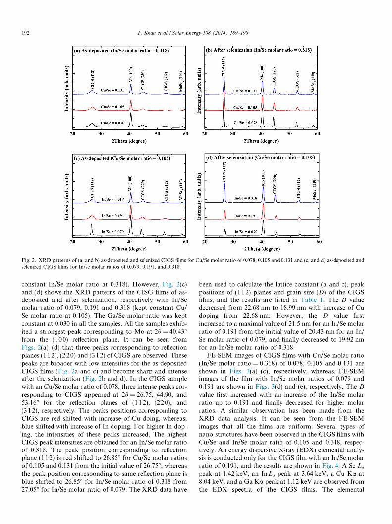
Fig. 2. XRD patterns of (a, and b) as-deposited and selenized CIGS films for Cu/Se molar ratio of 0.078, 0.105 and 0.131 and (c, and d) as-deposited andselenized CIGS films for In/se molar ratios of 0.079, 0.191, and 0.318.
192 F. Khan et al. / Solar Energy 108 (2014) 189–198
constant In/Se molar ratio at 0.318). However, Fig. 2(c)and (d) shows the XRD patterns of the CISG films of as-deposited and after selenization, respectively with In/Semolar ratio of 0.079, 0.191 and 0.318 (kept constant Cu/Se molar ratio at 0.105). The Ga/Se molar ratio was keptconstant at 0.030 in all the samples. All the samples exhib-ited a strongest peak corresponding to Mo at 2h = 40.43�from the (100) reflection plane. It can be seen fromFigs. 2(a)–(d) that three peaks corresponding to reflectionplanes (112), (220) and (312) of CIGS are observed. Thesepeaks are broader with low intensities for the as depositedCIGS films (Fig. 2a and c) and become sharp and intenseafter the selenization (Fig. 2b and d). In the CIGS samplewith an Cu/Se molar ratio of 0.078, three intense peaks cor-responding to CIGS appeared at 2h = 26.75, 44.90, and53.16� for the reflection planes of (11 2), (22 0), and(312), respectively. The peaks positions corresponding toCIGS are red shifted with increase of Cu doing, whereas,blue shifted with increase of In doping. For higher In dop-ing, the intensities of these peaks increased. The highestCIGS peak intensities are obtained for an In/Se molar ratioof 0.318. The peak position corresponding to reflectionplane (112) is red shifted to 26.85� for Cu/Se molar ratiosof 0.105 and 0.131 from the initial value of 26.75�, whereasthe peak position corresponding to same reflection plane isblue shifted to 26.85� for In/Se molar ratio of 0.318 from27.05� for In/Se molar ratio of 0.079. The XRD data have
been used to calculate the lattice constant (a and c), peakpositions of (112) planes and grain size (D) of the CIGSfilms, and the results are listed in Table 1. The D valuedecreased from 22.68 nm to 18.99 nm with increase of Cudoping from 22.68 nm. However, the D value firstincreased to a maximal value of 21.5 nm for an In/Se molarratio of 0.191 from the initial value of 20.43 nm for an In/Se molar ratio of 0.079, and finally decreased to 19.92 nmfor an In/Se molar ratio of 0.318.
FE-SEM images of CIGS films with Cu/Se molar ratio(In/Se molar ratio = 0.318) of 0.078, 0.105 and 0.131 areshown in Figs. 3(a)–(c), respectively, whereas, FE-SEMimages of the film with In/Se molar ratios of 0.079 and0.191 are shown in Figs. 3(d) and (e), respectively. The D
value first increased with an increase of the In/Se molarratio up to 0.191 and finally decreased for higher molarratios. A similar observation has been made from theXRD data analysis. It can be seen from the FE-SEMimages that all the films are uniform. Several types ofnano-structures have been observed in the CIGS films withCu/Se and In/Se molar ratio of 0.105 and 0.318, respec-tively. An energy dispersive X-ray (EDX) elemental analy-sis is conducted only for the CIGS film with an In/Se molarratio of 0.191, and the results are shown in Fig. 4. A Se La
peak at 1.42 keV, an InLa peak at 3.64 keV, a Cu Ka at8.04 keV, and a Ga Ka peak at 1.12 keV are observed fromthe EDX spectra of the CIGS films. The elemental
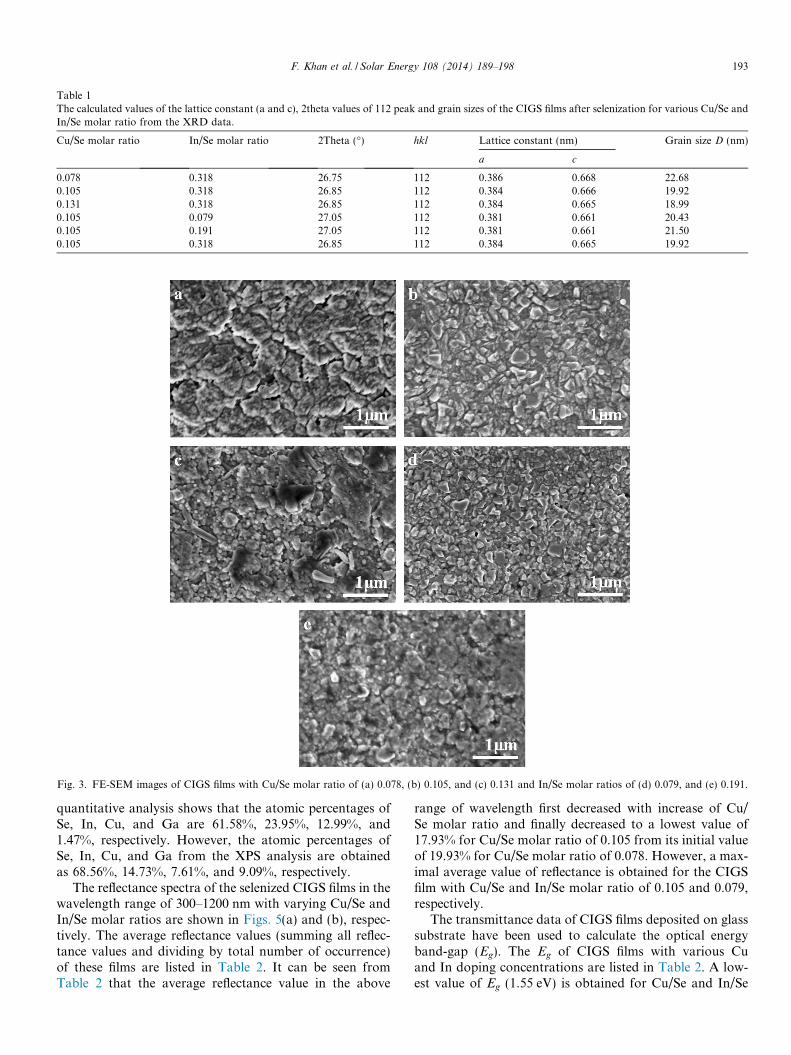
Table 1The calculated values of the lattice constant (a and c), 2theta values of 112 peak and grain sizes of the CIGS films after selenization for various Cu/Se andIn/Se molar ratio from the XRD data.
Cu/Se molar ratio In/Se molar ratio 2Theta (�) hkl Lattice constant (nm) Grain size D (nm)
a c
0.078 0.318 26.75 112 0.386 0.668 22.680.105 0.318 26.85 112 0.384 0.666 19.920.131 0.318 26.85 112 0.384 0.665 18.990.105 0.079 27.05 112 0.381 0.661 20.430.105 0.191 27.05 112 0.381 0.661 21.500.105 0.318 26.85 112 0.384 0.665 19.92
Fig. 3. FE-SEM images of CIGS films with Cu/Se molar ratio of (a) 0.078, (b) 0.105, and (c) 0.131 and In/Se molar ratios of (d) 0.079, and (e) 0.191.
F. Khan et al. / Solar Energy 108 (2014) 189–198 193
quantitative analysis shows that the atomic percentages ofSe, In, Cu, and Ga are 61.58%, 23.95%, 12.99%, and1.47%, respectively. However, the atomic percentages ofSe, In, Cu, and Ga from the XPS analysis are obtainedas 68.56%, 14.73%, 7.61%, and 9.09%, respectively.
The reflectance spectra of the selenized CIGS films in thewavelength range of 300–1200 nm with varying Cu/Se andIn/Se molar ratios are shown in Figs. 5(a) and (b), respec-tively. The average reflectance values (summing all reflec-tance values and dividing by total number of occurrence)of these films are listed in Table 2. It can be seen fromTable 2 that the average reflectance value in the above
range of wavelength first decreased with increase of Cu/Se molar ratio and finally decreased to a lowest value of17.93% for Cu/Se molar ratio of 0.105 from its initial valueof 19.93% for Cu/Se molar ratio of 0.078. However, a max-imal average value of reflectance is obtained for the CIGSfilm with Cu/Se and In/Se molar ratio of 0.105 and 0.079,respectively.
The transmittance data of CIGS films deposited on glasssubstrate have been used to calculate the optical energyband-gap (Eg). The Eg of CIGS films with various Cuand In doping concentrations are listed in Table 2. A low-est value of Eg (1.55 eV) is obtained for Cu/Se and In/Se
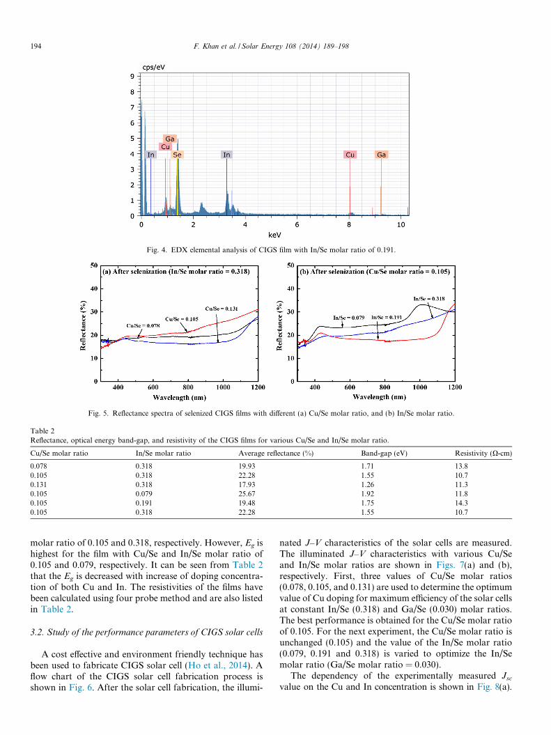
Fig. 5. Reflectance spectra of selenized CIGS films with different (a) Cu/Se molar ratio, and (b) In/Se molar ratio.
Fig. 4. EDX elemental analysis of CIGS film with In/Se molar ratio of 0.191.
Table 2Reflectance, optical energy band-gap, and resistivity of the CIGS films for various Cu/Se and In/Se molar ratio.
Cu/Se molar ratio In/Se molar ratio Average reflectance (%) Band-gap (eV) Resistivity (X-cm)
0.078 0.318 19.93 1.71 13.80.105 0.318 22.28 1.55 10.70.131 0.318 17.93 1.26 11.30.105 0.079 25.67 1.92 11.80.105 0.191 19.48 1.75 14.30.105 0.318 22.28 1.55 10.7
194 F. Khan et al. / Solar Energy 108 (2014) 189–198
molar ratio of 0.105 and 0.318, respectively. However, Eg ishighest for the film with Cu/Se and In/Se molar ratio of0.105 and 0.079, respectively. It can be seen from Table 2that the Eg is decreased with increase of doping concentra-tion of both Cu and In. The resistivities of the films havebeen calculated using four probe method and are also listedin Table 2.
3.2. Study of the performance parameters of CIGS solar cells
A cost effective and environment friendly technique hasbeen used to fabricate CIGS solar cell (Ho et al., 2014). Aflow chart of the CIGS solar cell fabrication process isshown in Fig. 6. After the solar cell fabrication, the illumi-
nated J–V characteristics of the solar cells are measured.The illuminated J–V characteristics with various Cu/Seand In/Se molar ratios are shown in Figs. 7(a) and (b),respectively. First, three values of Cu/Se molar ratios(0.078, 0.105, and 0.131) are used to determine the optimumvalue of Cu doping for maximum efficiency of the solar cellsat constant In/Se (0.318) and Ga/Se (0.030) molar ratios.The best performance is obtained for the Cu/Se molar ratioof 0.105. For the next experiment, the Cu/Se molar ratio isunchanged (0.105) and the value of the In/Se molar ratio(0.079, 0.191 and 0.318) is varied to optimize the In/Semolar ratio (Ga/Se molar ratio = 0.030).
The dependency of the experimentally measured Jsc
value on the Cu and In concentration is shown in Fig. 8(a).
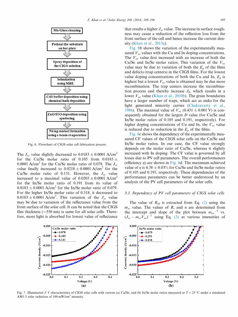
Fig. 6. Flowchart of CIGS solar cell fabrication process.
F. Khan et al. / Solar Energy 108 (2014) 189–198 195
The Jsc value slightly decreased to 0.0183 ± 0.0001 A/cm2
for the Cu/Se molar ratio of 0.105 from 0.0185 ±0.0001 A/cm2 for the Cu/Se molar ratio of 0.078. The Jsc
value finally increased to 0.0218 ± 0.0001 A/cm2 for theCu/Se molar ratio of 0.131. However, the Jsc valueincreased to a maximal value of 0.0203 ± 0.0001 A/cm2
for the In/Se molar ratio of 0.191 from its value of0.0183 ± 0.0001 A/cm2 for the In/Se molar ratio of 0.079.For the higher In/Se molar ratio of 0.318, it decreased to0.0183 ± 0.0001 A/cm2. This variation of the Jsc valuemay be due to variation of the reflectance value from thefront surface of the solar cell. It can be noted that the CIGSfilm thickness (�550 nm) is same for all solar cells. There-fore, more light is absorbed for lowest value of reflectance
Fig. 7. Illuminated J–V characteristics of CIGS solar cells with various (a) CuAM1.5 solar radiation of 100 mW/cm2 intensity.
that results a higher Jsc value. The increase in surface rough-ness may cause a reduction of the reflection loss from thefront surface of the cell and hence increase the current den-sity (Khan et al., 2013a).
Fig. 8b shows the variation of the experimentally mea-sured Voc values with the Cu and In doping concentrations.The Voc value first increased with an increase of both theCu/Se and In/Se molar ratios. This variation of the Voc
value may be due to variation of both the Eg of the filmsand defects (trap centers) in the CIGS films. For the lowestvalue doping concentrations of both the Cu and In, Eg ishighest but a lowest Voc value is obtained may be due morerecombination. The trap centers increase the recombina-tion process and thereby increase J0, which results in alower Voc value (Khan et al., 2010b). The grain boundarieshave a larger number of traps, which act as sinks for thelight generated minority carries (Chakravarty et al.,1986). The maximal value of Voc (0.431 ± 0.001 V) is con-sequently obtained for the largest D value (for Cu/Se andIn/Se molar ratios of 0.105 and 0.191, respectively). Forhigher doping concentrations of Cu and In, the Voc valueis reduced due to reduction in the Eg of the films.
Fig. 8c shows the dependency of the experimentally mea-sured CF values of the CIGS solar cells on the Cu/Se andIn/Se molar ratios. In our case, the CF value stronglydepends on the molar ratio of Cu/Se, whereas it slightlyincreased with In doping. The CF value is governed by alllosses due to PV cell parameters. The overall performances(efficiency g) are shown in Fig. 8d. The maximum achievedvalue of g is 4.38 ± 0.03% for Cu/Se and In/Se molar ratiosof 0.105 and 0.191, respectively. These dependencies of theperformance parameters can be better understood by ananalysis of the PV cell parameters of the solar cells.
3.3. Dependency of PV cell parameters of CIGS solar cells
The value of Rsh is extracted from Eq. (2) using themsc value. The values of Rs and n are determined fromthe intercept and slope of the plot between moc
�1 vs.(Jsc � mscVoc)
�1 using Eq. (3) at various intensities of
/Se, and (b) In/Se molar ratios measured at T = 25 �C under a simulated
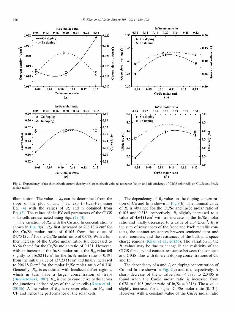
Fig. 8. Dependency of (a) short circuit current density, (b) open circuit voltage, (c) curve factor, and (d) efficiency of CIGS solar cells on Cu/Se and In/Semolar ratios.
196 F. Khan et al. / Solar Energy 108 (2014) 189–198
illumination. The value of J0 can be determined from theslope of the plot of moc
�1 vs. exp (�Voc/nVT) usingEq. (4) with the values of Rs and n obtained fromEq. (3). The values of the PV cell parameters of the CIGSsolar cells are extracted using Eqs. (2)–(4).
The variation of Rsh with the Cu and In concentration isshown in Fig. 9(a). Rsh first increased to 206.18 X cm2 forthe Cu/Se molar ratio of 0.105 from the value of84.75 X cm2 for the Cu/Se molar ratio of 0.078. With a fur-ther increase of the Cu/Se molar ratio, Rsh decreased to83.54 X cm2 for the Cu/Se molar ratio of 0.131. However,with an increase of the In/Se molar ratio, the Rsh value fellslightly to 116.82 X cm2 for the In/Se molar ratio of 0.191from the initial value of 127.23 X cm2 and finally increasedto 206.18 X cm2 for the molar In/Se molar ratio of 0.318.Generally, Rsh is associated with localized defect regions,which in turn have a larger concentration of traps(Broniatowski, 1987). Rsh is due to conductive paths acrossthe junctions and/or edges of the solar cells (Khan et al.,2013b). A low value of Rsh have sever effects on Voc andCF and hence the performance of the solar cells.
The dependency of Rs value on the doping concentra-tion of Cu and In is shown in Fig 9(b). The minimal valueof Rs is obtained for the Cu/Se and In/Se molar ratio of0.105 and 0.318, respectively. Rs slightly increased to avalue of 4.64 X cm2 with an increase of the In/Se molarratio and finally decreased to a value of 2.34 X cm2. Rs isthe sum of resistances of the front and back metallic con-tacts, the contact resistances between semiconductor andmetal contacts, and the resistances of the bulk and spacecharge regions (Khan et al., 2013b). The variation in theRs values may be due to change in the resistivity of theCIGS films or/and contact resistance between the contactsand CIGS films with different doping concentrations of Cuand In.
The dependency of n and J0 on doping concentration ofCu and In are shown in Fig. 9(c) and (d), respectively. Asharp decrease of the n value from 4.5375 to 2.3405 isfound when the Cu/Se molar ratio is increased from0.078 to 0.105 (molar ratio of In/Se = 0.318). The n valueslightly increased for a higher Cu/Se molar ratio (0.131).However, with a constant value of the Cu/Se molar ratio
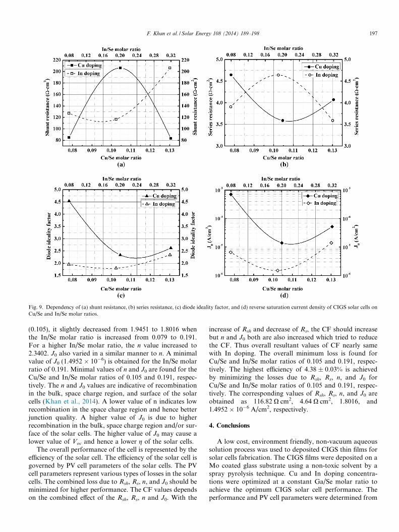
Fig. 9. Dependency of (a) shunt resistance, (b) series resistance, (c) diode ideality factor, and (d) reverse saturation current density of CIGS solar cells onCu/Se and In/Se molar ratios.
F. Khan et al. / Solar Energy 108 (2014) 189–198 197
(0.105), it slightly decreased from 1.9451 to 1.8016 whenthe In/Se molar ratio is increased from 0.079 to 0.191.For a higher In/Se molar ratio, the n value increased to2.3402. J0 also varied in a similar manner to n. A minimalvalue of J0 (1.4952 � 10�6) is obtained for the In/Se molarratio of 0.191. Minimal values of n and J0 are found for theCu/Se and In/Se molar ratios of 0.105 and 0.191, respec-tively. The n and J0 values are indicative of recombinationin the bulk, space charge region, and surface of the solarcells (Khan et al., 2014). A lower value of n indicates lowrecombination in the space charge region and hence betterjunction quality. A higher value of J0 is due to higherrecombination in the bulk, space charge region and/or sur-face of the solar cells. The higher value of J0 may cause alower value of Voc and hence a lower g of the solar cells.
The overall performance of the cell is represented by theefficiency of the solar cell. The efficiency of the solar cell isgoverned by PV cell parameters of the solar cells. The PVcell parameters represent various types of losses in the solarcells. The combined loss due to Rsh, Rs, n, and J0 should beminimized for higher performance. The CF values dependson the combined effect of the Rsh, Rs, n and J0. With the
increase of Rsh and decrease of Rs, the CF should increasebut n and J0 both are also increased which tried to reducethe CF. Thus overall resultant values of CF nearly samewith In doping. The overall minimum loss is found forCu/Se and In/Se molar ratios of 0.105 and 0.191, respec-tively. The highest efficiency of 4.38 ± 0.03% is achievedby minimizing the losses due to Rsh, Rs, n, and J0 forCu/Se and In/Se molar ratios of 0.105 and 0.191, respec-tively. The corresponding values of Rsh, Rs, n, and J0 areobtained as 116.82 X cm2, 4.64 X cm2, 1.8016, and1.4952 � 10�6 A/cm2, respectively.
4. Conclusions
A low cost, environment friendly, non-vacuum aqueoussolution process was used to deposited CIGS thin films forsolar cells fabrication. The CIGS films were deposited on aMo coated glass substrate using a non-toxic solvent by aspray pyrolysis technique. Cu and In doping concentra-tions were optimized at a constant Ga/Se molar ratio toachieve the optimum CIGS solar cell performance. Theperformance and PV cell parameters were determined from
198 F. Khan et al. / Solar Energy 108 (2014) 189–198
the illuminated J–V characteristics to carry out a loss anal-ysis of the solar cell. Maximum short circuit current densityof 0.0218 ± 0.0001 A/cm2 is achieved for Cu/Se and In/Semolar ratios of 0.131 and 0.318, respectively. However, dueto lower Voc and CF values, a lower efficiency is obtained.The maximum value of Voc is found to be 0.431 ± 0.001 Vfor Cu/Se and In/Se molar ratios of 0.105 and0.191, respectively. The maximal achieved efficiency is4.38 ± 0.03%, obtained with the lowest n and J0 values.The corresponding values of Rsh, Rs, n and J0 are obtainedas 116.82 X cm2, 4.64 X cm2, 1.802, and 1.495 � 10�6 A/cm2, respectively.
Acknowledgements
This work was financially supported by the PioneerResearch Center Program through the National ResearchFoundation of South Korea (2011-0001649), Ministry ofScience, ICT and Future Planning (MSIP). Also partiallyfunded by the Energy International CollaborationResearch & Development Program of the Ministry ofTrade, Industry & Energy (MOTIE) (2011-8520010050),South Korea.
References
Ahn, S.J., Kim, C.W., Yun, J.H., Gwak, J.H., Jeong, S.H., Ryu, B.H.,Yoon, K.H., 2010. CuInSe2 (CIS) thin film solar cells by direct coatingand selenization of solution precursors. J. Phys. Chem. C 114, 8108–8113.
Broniatowski, A., 1987. Measurement of the grain-boundary states insemiconductors by deep-level transient spectroscopy. Phys. Rev. B 36,5895–5905.
Chakravarty, B.C., Arora, N.K., Singh, S.N., Das, B.K., 1986. Solar cellperformance with an inhomogeneous grain size distribution. IEEETrans. Electron Dev. ED-33, 158–160.
Cho, A., Ahn, S., Yun, J.H., Gwak, J., Ahn, S.K., Shin, K., Song, H.,Yoon, K.H., 2013. Non-vacuum processed CuInSe2 thin filmsfabricated with hybrid ink. Sol. Energy Mater. Sol. Cells 109,17–25.
Cliford, A.A., 1973. Multivariate Error Analysis: A Handbook of ErrorPropagation and Calculation in Many-Parameter Systems. Springer.
Guo, Q., Kim, S.J., Kar, M., Shafarman, W.N., Birkmire, R.W., Stach,E.A., Agrawal, R., Hillhouse, H.W., 2008. Development of CuInSe2
nanocrystal and nanoring inks for low-cost solar cells. Nano Lett. 8,2982–2987.
Ho, J.C.W., Zhang, T., Lee, K.K., Batabyal, S.K., Tok, A.I.Y., Wong,L.H., 2014. Spray pyrolysis of CuIn(S, Se)2 solar cells with 5.9%efficiency: A method to prevent Mo oxidation in ambient atmosphere.ACS Appl. Mater. Interfaces 6, 6638–6643.
Jackson, P., Hariskos, D., Lotter, E., Paetel, S., Wuerz, R., Menner, R.,Wischmann, W., Powalla, M., 2011. New world record efficiency forCu(In, Ga)Se2 thin-film solar cells beyond 20%. Prog. Photovolt.: Res.Appl. 19, 894–897.
Khan, F., Singh, S.N., Husain, M., 2010a. Determination of diodeparameters of a silicon solar cell from variation of slopes of the I–V
curve at open circuit and short circuit conditions with intensity ofillumination. Semicond. Sci. Technol. 25, 0150021–0150028.
Khan, F., Singh, S.N., Husain, M., 2010b. Effect of illumination intensityon cell parameters of a silicon solar cell. Sol. Energy. Mater. Sol. Cells94, 1473–1476.
Khan, F., 2011. Fabrication of diffused junction crystalline silicon solarcells with texturization and different antireflection coatings and studyof their photovoltaic properties. PhD Thesis, New Delhi, India.
Khan, F., Singh, S.N., Husain, M., 2011. Determination of the diodeparameters of a-Si and CdTe solar modules using variation of intensityof illumination: an application. Sol. Energy 85, 2288–2294.
Khan, F., Baek, S.H., Singh, S.N., Singh, P.K., Kim, J.H., 2013a.Effective passivation of silicon surface by AZO films: application inbifacial solar cells. Sol. Energy 97, 474–483.
Khan, F., Baek, S.H., Park, Y., Kim, J.H., 2013b. Extraction of diodeparameters of silicon solar cells under high illumination conditions.Energy Conver. Manage. 76, 421–429.
Khan, F., Baek, S.H., Mobin, A., Kim, J.H., 2014. Enhanced performanceof silicon solar cells by application of low-cost sol–gel-derived Al richZnO film. Sol. Energy 101, 265–271.
Kim, S.Y., Kim, J.H., 2012. Fabrication of CIGS thin films by using spraypyrolysis and post-selenization. J. Korean Phys. Soc. 60, 2018–2024.
Liu, W., Mitzi, D.B., Yuan, M., Kellock, A.J., Chey, S.J., Gunawan, O.,2010. 12% efficiency CuIn(Se, S)2 photovoltaic device prepared using ahydrazine solution process. Chem. Mater. 22, 1010–1014.
Malsch, I., 2003. Thin films seek a solar future. Ind. Phys. Mag. 9, 16.Mitzi, D.B., Yuan, M., Liu, W., Kellock, A.J., Chey, S.J., Deline, V.,
Schrott, A.G., 2008. A high-efficiency solution-deposited thin-filmphotovoltaic device. Adv. Mater. 20, 3657–3662.
Schulz, D.L., Curtis, C.J., Flitton, R.A., Weisner, H., Keane, J., Matson,R.J., Jones, K.M., Parilla, P.A., Noufi, R., Ginley, D.S., 1998. Cu–In–Ga–Se nanoparticle colloids as spray deposition precursors for Cu(In,Ga)Se2 solar cell materials. J. Electron. Mater. 27, 433–437.