High-Bandwidth Address Generation Unit
12
J Sign Process Syst DOI 10.1007/s11265-008-0174-x High-bandwidth Address Generation Unit Carlo Galuzzi · Chunyang Gou · Humberto Calderón · Georgi N. Gaydadjiev · Stamatis Vassiliadis Received: 22 October 2007 / Accepted: 4 March 2008 © The Author(s) 2008 Abstract In this paper we present an efficient data fetch circuitry to retrieve several operands from a n-way parallel memory system in a single machine cycle. The proposed address generation unit operates with an improved version of the low-order parallel memory access approach. Our design supports data structures of arbitrary lengths and different odd strides. The experimental results show that our address gen- eration unit is capable of generating eight 32 − bit addresses every 6 ns for different strides when imple- mented on a VIRTEX-II PRO xc2vp30-7ff1696 FPGA device using only trivial hardware resources. Keywords Address generation unit · Parallel memory · Stride 1 Introduction Vector architectures were originally adopted for build- ing supercomputers in 1970s [1]. Since then, they have Prof. Dr. Stamatis Vassiliadis has passed away. C. Galuzzi (B ) · C. Gou · H. Calderón · G. N. Gaydadjiev · S. Vassiliadis Computer Engineering Laboratory, Electrical Engineering, Mathematics and Computer Science Faculty, TU Delft, Delft, The Netherlands e-mail: [email protected] C. Gou e-mail: [email protected] H. Calderón e-mail: [email protected] G. N. Gaydadjiev e-mail: [email protected] played a central role in conventional supercomputers and have flourished for almost two decades till the appearance of the “vector aware” microprocessors in the early 1990s. The most successful ones include the Cray series [2] and the NEC SX series [3]. Nowadays, with the advance of the integration tech- nology, more and more transistors can be integrated on a single chip. Consequently, the SIMD processing paradigm (including vector execution model) regains its position in the organization of on-chip computa- tion resources, such as the General Purpose Processors (GPP) SIMD enhancements [4–6] and vector accel- erators in more specific application domains such as home entertainment [7] and computer graphics [8]. In order to provide sufficient and sustained bandwidth and to reduce memory access latency, parallel (multibank) memories are widely used in these SIMD processing systems [2, 3, 8]. A fast and efficient address generation for the memory subsystem is one of the key issues in system design when many memory banks work in parallel. This paper deals with the address generation problem of on-chip vector accelerators. More specif- ically, the main contributions of this paper are the following: – the design of an address generation unit (AGEN) capable of generating eight 32 − bit addresses in a single machine cycle. Arbitrary memory sequences are supported by using only one special purpose instruction; – an organization that uses optimized Boolean equa- tions to generate the offsets instead of including an additional adder stage; – an FPGA implementation of the proposed design able to fetch 1.33 Giga operands per second from an
Transcript of High-Bandwidth Address Generation Unit

J Sign Process SystDOI 10.1007/s11265-008-0174-x
High-bandwidth Address Generation Unit
Carlo Galuzzi · Chunyang Gou · Humberto Calderón ·Georgi N. Gaydadjiev · Stamatis Vassiliadis
Received: 22 October 2007 / Accepted: 4 March 2008© The Author(s) 2008
Abstract In this paper we present an efficient datafetch circuitry to retrieve several operands from an-way parallel memory system in a single machinecycle. The proposed address generation unit operateswith an improved version of the low-order parallelmemory access approach. Our design supports datastructures of arbitrary lengths and different odd strides.The experimental results show that our address gen-eration unit is capable of generating eight 32 − bitaddresses every 6 ns for different strides when imple-mented on a VIRTEX-II PRO xc2vp30-7ff1696 FPGAdevice using only trivial hardware resources.
Keywords Address generation unit ·Parallel memory · Stride
1 Introduction
Vector architectures were originally adopted for build-ing supercomputers in 1970s [1]. Since then, they have
Prof. Dr. Stamatis Vassiliadis has passed away.
C. Galuzzi (B) · C. Gou · H. Calderón ·G. N. Gaydadjiev · S. VassiliadisComputer Engineering Laboratory, Electrical Engineering,Mathematics and Computer Science Faculty,TU Delft, Delft, The Netherlandse-mail: [email protected]
C. Goue-mail: [email protected]
H. Calderóne-mail: [email protected]
G. N. Gaydadjieve-mail: [email protected]
played a central role in conventional supercomputersand have flourished for almost two decades till theappearance of the “vector aware” microprocessors inthe early 1990s. The most successful ones include theCray series [2] and the NEC SX series [3].
Nowadays, with the advance of the integration tech-nology, more and more transistors can be integratedon a single chip. Consequently, the SIMD processingparadigm (including vector execution model) regainsits position in the organization of on-chip computa-tion resources, such as the General Purpose Processors(GPP) SIMD enhancements [4–6] and vector accel-erators in more specific application domains such ashome entertainment [7] and computer graphics [8]. Inorder to provide sufficient and sustained bandwidth andto reduce memory access latency, parallel (multibank)memories are widely used in these SIMD processingsystems [2, 3, 8]. A fast and efficient address generationfor the memory subsystem is one of the key issuesin system design when many memory banks work inparallel. This paper deals with the address generationproblem of on-chip vector accelerators. More specif-ically, the main contributions of this paper are thefollowing:
– the design of an address generation unit (AGEN)capable of generating eight 32 − bit addresses in asingle machine cycle. Arbitrary memory sequencesare supported by using only one special purposeinstruction;
– an organization that uses optimized Boolean equa-tions to generate the offsets instead of including anadditional adder stage;
– an FPGA implementation of the proposed designable to fetch 1.33 Giga operands per second from an

C. Galuzzi et al.
Figure 1 Two paradigms ofvector address generation:a centralized, b distributed.
Memory
Module 0
Memory
Module 7
Row
address 0
Row
address 7
Vector Add ress
Generator
Vector Controller
B, S
Local address 0
Local address 0Switch
Module
assignment 0...7
Address
RoutingMemory
Module 0
f0 (B, S)
Local address 7
Vector Controller
B, S
Local address 7
Memory
Module 7
f7 (B, S)
a
b
8-way-parallel memory system using only 3% ofthe slices and only 4% of the lookup tables(LUTs) of the targeted device, the VIRTEX-IIPRO xc2vp30-7ff1696 FPGA.
The paper is organized as follows. In Sections 2 back-ground information and related works are provided. InSection 3 and 4, the basic definitions and the design ofthe proposed AGEN are presented. An outline of theexperimental results is given in Section 5. Concludingremarks and an outline of conducted research are givenin Section 6.
2 Background and Related Work
One of the main issues in vector processing systemswith multi-bank or multi-module memories is the ad-dress generation. There are two major paradigms foraddress generation: centralized and distributed. When-ever a vector memory access command comes in cen-tralized address generation, the base address as wellas the stride1 are sent to the AGEN, just as shown inFig. 1a. The centralized address generation paradigmis widely used in traditional vector supercomputers.In centralized AGEN, local addresses of all memorymodules are calculated and distributed to the corre-sponding modules using the address routing circuit (e.g.a crossbar) under the guidance of the correspondingmodule assignments. In the distributed AGEN, insteadof sending individual addresses to each memory mod-
1A formal definition of stride is presented in Section 3. Anyhow,the stride is the address distance between two consecutive dataelements stored in a memory system.
ule, Corbal et al. proposed a Command Vector Memory(CVM) System [9] that broadcasts the vector accesscommand to all memory modules simultaneously. Thelocal addresses of each memory module are then calcu-lated independently by the local module controller, asillustrated in Fig. 1b. Note that in Fig. 1, fi(B, S)(i = 0,
1, . . . , 7) are the local address generation functionswhere B and S denote the vector base and stride,respectively. It is shown in Fig. 1 that the address rout-ing circuitry is successfully removed by the distributedaddress generation scheme. Additionally, in [9] theauthors have demonstrated the feasibility of this mem-ory organization with simulations at the architecturallevel of a CVM coupled with an out-of-order vectorprocessor.
There are two clear advantages using the distrib-uted address generation. First, the local address routingcircuit can be substantially simplified (usually from acrossbar to a bus), that potentially allows for shorterdata access latencies. Second, since there can be morethan one memory address seen by the local modulecontroller, a distributed address generation can exploitin a better way the internal features of the module toimprove performance. This is the case, for example,when there are more than one access going to thesame memory module on a long vector access commandor when multiple vector commands are queued in themodule controller. In the CVM system, each memorymodule is a commodity SDRAM module with internalbanks and row buffers. The performance of the mem-ory system can therefore be enhanced by properly andindependently scheduling of the address sequences oneach module to increase the row buffer hit rate.
An extension of the work presented in [9] is pro-posed by Mathew et al. in [10, 11] where the authors

High-bandwidth address generation unit
proposed a Parallel Vector Access unit (PVA). Thisunit is a vector memory subsystem that provided strideddata accesses with high efficiency on a multi-moduleSDRAM memory. The PVA unit adopts the same ideaof the CVM system when it transmits vector commandsinstead of individual addresses to memory modules,and lets the modules independently determine whichaddresses are requested from them and how to pro-vide these requests. The authors, not only providedarchitectural simulation and the hardware design of thememory control unit but they also validated the designthrough gate-level simulation.
In order to perform PVA in command-based mem-ory system, one of the key points is the use of distrib-uted high-bandwidth address generation mechanismscapable of inferring which addresses are requestedfrom the local memory module. However, there ex-ist no progress work reported in the literature thatfocuses on the study of address generation circuitriesfor distributed address generation. The high-bandwidthAGEN proposed in this paper unravels the designissues by providing a case study for the distributedaddress generation.
Besides memory address generation, another criticaldesign consideration in multi-bank memory systems isthe distribution of the data within the different memorybanks to ensure maximum benefits from multi-bankmemory organization. One simple low-order interleav-ing scheme which maps address a to bank (a mod m)at local address (offset) (a div m) is easy to imple-ment, when m is a power of two, and the stride equalsone.2 Unfortunately, when the stride is different thanone, there is a large performance degradation due tobank conflicts [12]. To cope with this problem, manyresearchers focused their work on parallel memoryschemes. Two categories are identified: memory sys-tems with redundancy and memory system withoutredundancy [13]. An illustrative example of the firstcategory is represented by the prime memory systems.These systems are used by many researchers and re-search projects [14–17] and are built upon previouswork on prime numbers. The drawback of these sys-tems is the modulo operation on prime numbers whichis difficult to implement efficiently in hardware. Anexample of the second category is represented by theskewing memory systems including the widely used rowrotation schemes and XOR schemes [18–24].
The focus of our paper is on the high-bandwidthaddress generation circuitry for multi-bank memory
2Given two integers a and b we have a=bq + r where a div b =qis the quotient and a mod b = r is the rest, with a, b , q, r ∈ N andq, r univocally determined.
0
0 1 2 3 4 5 6 7 0 1 2 3 4 5 6 7
1
2
3
4
.
.
.
m
0
1
2
3
4
.
.
.
m
a bFigure 2 An example of a memory system composed by 8 banksof memory, each one holding the same number of memory cells,where 8 data are stored in two different ways: a in a consecutiveway, b leaving a fix number of cells between the data.
systems with low-order interleaving scheme. Althoughthe details of vector address generation is closely re-lated to the memory schemes that the vector process-ing systems adopt, we believe that the methodologiespresented in this paper may also be of interest for ad-dress generation circuitry under other parallel memoryschemes.
3 Theoretical Background
In this section, we begin by introducing a motivatingexample to informally outline the main concepts of theproposed method. Thereafter we present the theoreti-cal foundation of our approach.
3.1 Motivating Example
Let us consider a memory system composed by n banksof memory each holding m memory cells. The m × nmemory cells can be represented by a matrix [m × n]where each column corresponds to a memory bank.Let us consider the data a0, ..., an−1 to store in themain memory system. Let us assume the element a0 isidentified by the pair of indexes (i0, j0) in the matrixrepresenting the memory. The data are stored per rowin a circular way: when a data aα is stored in position(iα, n − 1) then aα+1 is stored in position (iα + 1, 0). Letus assume to store the data leaving a certain num-ber of cells S between two consecutive data elements.Then aα is identified by the pair of indexes: iα = iα−1+( jα−1 + S) div n and jα = ( jα−1 + S) mod n.
In Fig. 2, we present two examples of storing 8 dataelements in a memory system composed by 8 memorybanks, each one holding the same number of mem-ory cells. In Fig. 2a the data are stored consecutivelywhereas in Fig. 2b the data are stored leaving a fixednumber of cells between two consecutive elements. Asthe figure shows, the 8 elements belong to different

C. Galuzzi et al.
memory banks. This means that 8 data can be read inparallel without problem of conflict in a single cycle ifwe are able to design an AGEN capable of generatingthe eight addresses.
3.2 Theoretical Foundation of the AGEN Design
Definition 1 We call stride the address distance be-tween two consecutive data elements stored in a mem-ory system.
Roughly speaking, the address distance betweentwo consecutive data is represented by the number ofcells separating the two elements per row as describedabove. The stride is clearly an integer number.
Let us consider n banks of memory each one holdingm memory cells. The m × n memory cells can be rep-resented as a matrix [m × n] where each column cor-responds to a memory bank. In addition, the memorycell i of the memory bank j corresponds to the matrixelement with indexes (i, j ). We denote this matrix asA and consider n = 2h and m for its dimensions, withh, m ∈ N. Additionally, the stride is an integer Str =2q + 1, q ∈ N. From now on, the data stored in thememory banks will be considered as matrix A elements.Let the n consecutive data placed in the memory banksbe denoted by:
a0, ..., an−1. (1)
Remark 1 Every element aα , with α = 0, ..., n − 1, isidentified in the matrix by its row-index i, with i = 0,
1, ..., m − 1, and its column-index j, with j = 0, 1, ...,
n − 1. Additionally, the pair of indexes (iα, jα) can beused to represent aα as a number in base n, obtain-able as juxtaposition of iα as most significant digit andjα as least significant digit. The two indexes can alsobe used in a base 10 representation. Therefore, wehave the following chain of equivalent representationsfor aα :
aα ↔ (iα, jα) ↔ (iα jα)|n ↔ (niα + jα)|10. (2)
The usefulness of this result will be more clear in theproof of Theorem 1. As an example, Table 1 shows thepair of indexes identifying the data in the matrix forn = 8 and Str = 3 (Fig. 2b), assuming (i0, j0) = (0, 0).
Remark 2 Without loss of generality, we can assumethat the first element a0 stored in the matrix remainsat position (i0, j0) = (0, 0).
Lemma 1 The number of rows necessary to hold nelements with stride Str = 2q + 1, q ∈ N is Str.
Table 1 Correspondence aα ↔ (iα, jα) ↔ aα|n ↔ aα|10 for n = 8and Str = 3.
Element aα Row-index iα Column-index jα aα|8 aα|10
a0 0 0 00 0a1 0 3 03 3a2 0 6 06 6a3 1 1 11 9a4 1 4 14 12a5 1 7 17 15a6 2 2 22 18a7 2 5 25 21
Proof The number of cells (�cell) necessary to storen elements with stride Str is �cell = n + (Str − 1) n =n(2q + 1). Therefore, the number of rows is:
�cell mod n = n(Str) mod n = Str. (3)
��
Remark 2 and Lemma 1 imply that the necessaryrows to store the n elements with stride Str are:
{0, 1, ..., Str − 1} (4)
As an example, in Fig. 2b it is possible to see that theeight data are stored in 3 rows (Str = 3).
The n data aα can be defined recursively. If a0 =(i0, j0) the elements a2, ..., an−1 can be recursively de-fined as follows:
aα = aα−1 + Str. (5)
This is equivalent to the following: given aα−1 identifiedby the pair of indexes (iα−1, jα−1), aα is identified by thepair of indexes:
iα = iα−1 + ( jα−1 + Str) div n
jα = ( jα−1 + Str) mod n (6)
Theorem 1 Let n be the number of elements aα , withα = 0, ..., n − 1, stored in a matrix A, m × n, with n =2h. Let the stride be the integer Str ∈ N. If (iα, jα) and(iβ, jβ) are the index pairs identifying aα and aβ in thematrix and gcd(n, Str) = 1, we have:
jα �= jβ ∀α, β ∈ [0, ..., n − 1]. (7)
Proof Without loss of generality, by Remark 2, we canassume (i0, j0) = (0, 0). By contradiction let jα = jβ .We have two possible cases: (1) iα = iβ and (2) iα �= iβ .
The first case does not occur: more precisely, if iα =iβ , the assumption jα = jβ leads to aα = aβ (see Remark

High-bandwidth address generation unit
1). In the second case: iα �= iβ . Firstly, by Eq. 4, itfollows:
iβ − iα ∈ [0, Str − 1]. (8)
Without loss of generality we can assume β > α. ByEq. 5 we have:
aβ = aβ−1 + Str = aβ−2 + 2Str = ... = aα + xStr, (9)
with x ∈ N and x < n; it is straightforward to show thatx = β − α. By using the representation in base 10 of aα
and aβ (see Eq. 2), Eq. 9 becomes:
niβ + jβ = niα + jα + x Str, (10)
taking into account the assumption jα = jβ we canrewrite Eq. 10 as
n(iβ − iα) = x Str. (11)
Since gcd(n, Str) = 1 and n divides the product x Str,it follows that n is a non trivial divisor of x (i.e. adivisor different from 1 and n). This implies that: x =r n, with r ∈ N. It follows x > n which contradicts theoriginal hypothesis. As a consequence, it must be thatjα �= jβ , for all α, β ∈ [0, ..., n − 1]. ��
The previous theorem implies the following:
(S): n data stored in n memory banks can be accessedin parallel in a single machine cycle if n is coprimewith the stride.
This because by Theorem 1 each data is stored in adifferent memory bank. This holds, in particular, if n =2h and Str is an odd integer and viceversa, n an oddinteger and Str = 2h.
Example 1 Let us consider Fig. 2b and Table 1. In thiscase n = 8 and Str= 3. In Column 3 of Table 1, it ispossible to see that each data stored in the system isallocated in a different memory bank. This follows byTheorem 1. If there exist two elements aα, aβ with thesame column index then there exists x < 8 such that:n(iβ − iα) = x(2q + 1) (q = 1 in this case). Consideringthat n = 8 in our example, n(iβ − iα) can be either 8 or16. The difference cannot be 0 since in that case iα = iβand therefore aα = aβ . As a consequence, we have twocases 8 = 3x or 16 = 3x and both equations do not havean integer solution for x.
Remark 3 Let the stride Str = 2q + 1 be and odd inte-ger. Let aα and aβ be two consecutive data located inthe same memory bank. Then |iβ − iα| = Str.
Proof Let aα and aβ be identified by the pairs ofindexes (iα, jα) and (iβ, jβ) respectively with jα = jβ .Without loss of generality we can assume iβ > iα . Bythe proof of Theorem 1, we know that if jα = jβ , then:
n(iβ − iα) = x Str. (12)
Therefore
(iβ − iα) = xn
Str. (13)
Since iβ − iα ∈ N, it means that x = pn with p ∈ N.Since aα and aβ are two consecutive data located in thesame memory bank, it means that x = minp∈N pn = n.Then
(iβ − iα) = nn
Str = Str. (14)
��
Previous remark can be reformulated saying that ifthe stride is an odd integer coprime with the number ofmemory banks, the distance between two consecutivedata belonging to the same banks of memory is equalto the stride and independent by i and j.
Theorem 3 Let a0 be identified by the pair of indexes(i0, j0) with j0 = 0 and let Str be an odd stride. For anelement aα we have that
iα = BS + Aα (15)
where BS= i0 + k Str with k ∈ N and Aα = φ(n, jα, Str)is a function of n, jα and Str.
Proof By Eq. 6 we can easily obtain the following:
iα = i0 + ( j0 + αStr) div n
jα = ( j0 + αStr) mod n (16)
Additionally, we know that from the algorithm of di-vision: given two integers a and b we have a = bq + rwhere a div b = q is the quotient and a mod b = r isthe rest, with a, b, q, r ∈ N and q, r univocally deter-mined. Combining these two results, if we considera = j0 + αStr and b = n, we obtain the following:j0 + αStr = n(iα − i0) + jα, (17)
and therefore we can obtain iα as follows:
iα = i0 + j0 − jα + αStrn
. (18)
C. Galuzzi et al.
Adding and subtracting the quantity k Str, sinceBS = i0 + k Str, we have the following:
iα = i0 + k Str + j0 − jα + αStrn
− k Str
= BS + j0 − jα + αStrn
− k Str. (19)
From Eq. 16, we have that:
jα = ( j0 + αStr) mod n. (20)
This means that there exists k1 ∈ N such that:j0 + αStr = jα + k1n
α = jα + k1n − j0Str
. (21)
This means that there exists a function ψ such thatα = ψ(n, jα, Str) ∈ N. As a consequence, we have:
iα = BS + j0 − jα + αStrn
− k Str
= BS + j0 − jα + Strψ(n, jα, Str)n
− k Str
= BS + φ(n, jα, Str) = BS + Aα.
(22)
where φ : N × N × N → N. ��
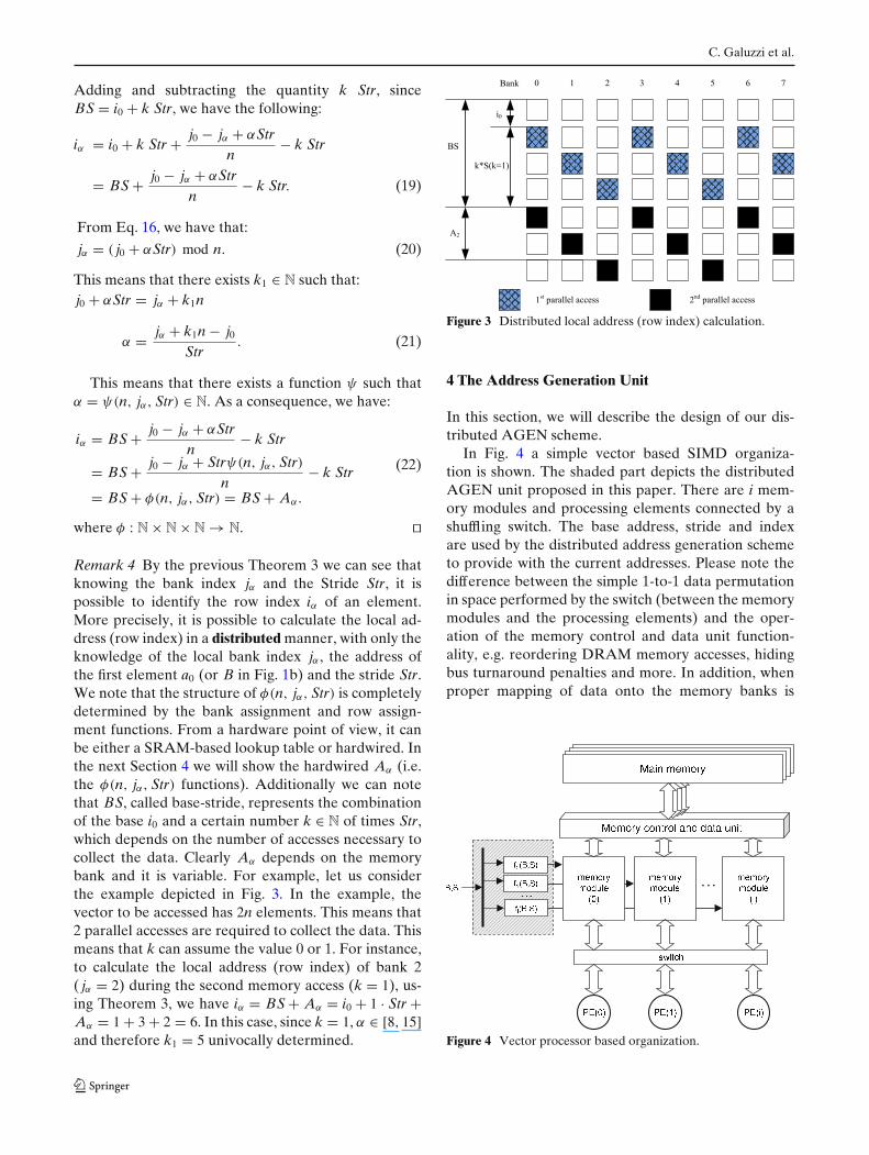
Remark 4 By the previous Theorem 3 we can see thatknowing the bank index jα and the Stride Str, it ispossible to identify the row index iα of an element.More precisely, it is possible to calculate the local ad-dress (row index) in a distributed manner, with only theknowledge of the local bank index jα , the address ofthe first element a0 (or B in Fig. 1b) and the stride Str.We note that the structure of φ(n, jα, Str) is completelydetermined by the bank assignment and row assign-ment functions. From a hardware point of view, it canbe either a SRAM-based lookup table or hardwired. Inthe next Section 4 we will show the hardwired Aα (i.e.the φ(n, jα, Str) functions). Additionally we can notethat BS, called base-stride, represents the combinationof the base i0 and a certain number k ∈ N of times Str,which depends on the number of accesses necessary tocollect the data. Clearly Aα depends on the memorybank and it is variable. For example, let us considerthe example depicted in Fig. 3. In the example, thevector to be accessed has 2n elements. This means that2 parallel accesses are required to collect the data. Thismeans that k can assume the value 0 or 1. For instance,to calculate the local address (row index) of bank 2( jα = 2) during the second memory access (k = 1), us-ing Theorem 3, we have iα = BS + Aα = i0 + 1 · Str +Aα = 1 + 3 + 2 = 6. In this case, since k = 1, α ∈ [8, 15]and therefore k1 = 5 univocally determined.
BS
A2
i0
k*S(k=1)
Bank 0 1 2 3 4 5 6 7
1st parallel access 2nd parallel access
Figure 3 Distributed local address (row index) calculation.
4 The Address Generation Unit
In this section, we will describe the design of our dis-tributed AGEN scheme.
In Fig. 4 a simple vector based SIMD organiza-tion is shown. The shaded part depicts the distributedAGEN unit proposed in this paper. There are i mem-ory modules and processing elements connected by ashuffling switch. The base address, stride and indexare used by the distributed address generation schemeto provide with the current addresses. Please note thedifference between the simple 1-to-1 data permutationin space performed by the switch (between the memorymodules and the processing elements) and the oper-ation of the memory control and data unit function-ality, e.g. reordering DRAM memory accesses, hidingbus turnaround penalties and more. In addition, whenproper mapping of data onto the memory banks is
Figure 4 Vector processor based organization.

High-bandwidth address generation unit
0 8 12 16 20 24 3128
Figure 5 The special-purpose-instruction [31].
applied, the switch can be avoided at all. This willadditionally slightly increase the system performance.Organization like this can be used for proposals withstrict demands on the timing of the address generationprocess as the ones presented in [25, 26].
Such organization can also be applied for polymor-phic computing systems as the one proposed in [27].The arbiter used to distribute the instructions betweenthe general purpose processor and the reconfigurablevector co-processor will provide the required controlinstructions at the exact moment in the instruction flow.Such an organization is assumed in the reminder of thissection.
We consider an 8-way parallel memory where thememory banks are built using dual ported memories,such as BRAMs [28], which in case of an implemen-tation on an FPGA are shared by the core processorand the vector co-processor (composed by the PE’s inthe figure). The 8 memory banks are arranged as a lin-ear array memory with low-order interleaving addressmapping [29] from the general purpose processor andthe memory controller side. The second BRAM portis used by the vector processing elements that see thememory organized as a 2D rectangular array [13]. Sincethe two memory accesses are decoupled in nature andthe address generation is critical for the SIMD perfor-mance, we will concentrate on the vector co-processorside.
When the vector co-processor needs to access thememory banks in parallel, the Effective Address (EA)computation impacts performance [30]. Our AGENunit (different from the one embedded into the mainmemory controller and the general purpose processor)which generates the addresses for the data stored inthe parallel memory in the correct sequence plays an
important role. Considering an 8-way parallel memory,8 different addresses for each memory access are neces-sary. The proposed AGEN generates those 8 addressesneeded to fetch the data simultaneously from the mem-ory at high rate. More specifically, as we will see inSection 5, the proposed AGEN is able to generate eight32-bit addresses every 6 ns for different odd strideswhen implemented in Xilinx FPGA technology.
Our AGEN unit is designed to work with single ormultiple groups of streamed data (with the same stride)using a special-purpose-instruction like in [31]. Thisinstruction configures the base addresses, the strideand the length of the particular streaming data format.Additionally, the memory accesses can be performed inparallel with the execution phase of a previous iterationusing a decoupled approach as presented in [32] and asshown in Fig. 4.
Figure 5 depicts an example of the special-purpose-instruction for operations with multiple indices such asSum of Absolute Differences operation (SAD) and/orMultiply-ACcumulate operation (MAC). More pre-cisely, the special-purpose-instruction contains the fol-lowing information:
– Basei (i = 1, 2, 3). These three fields contain thememory addresses of the data to read or writein the memory. For example, these fields can beused to store the minuend and subtrahend of theSAD operation or the multiplicand, multiplier andaddendum in the MAC operation.
– Length. This field contains the number of n-tuples(cycles) needed to fetch n elements from the mem-ory. For example, if Length = 10 and n = 8, in 10memory cycles 80 elements will be fetched.
– Stride. This field contains the address distance be-tween two consecutive data elements stored in an n-way parallel memory. In this paper we address onlythe odd strides between 1 and 15. Future researchwill include the analysis of the remaining cases.
Figure 6 AGEN:a accumulator for BScomputing, b accumulatorfor loop control, c hardwiredencoder, d indexaccumulator, e final additionEA computing.
Subtractor
Register
Hardwired Encoder
“Digitwise Strider”Adder
Register
3/2 counter
array
2/1 adder
3/2 counter
array
2/1 adder
3/2 counter
array
2/1 adder
3/2 counter
array
2/1 adder
3/2 counter
array
2/1 adder
3/2 counter
array
2/1 adder
3/2 counter
array
2/1 adder
3/2 counter
array
2/1 adder
Adder
Register

C. Galuzzi et al.
Figure 7 Main accumulatorcircuitry.
These 8 different strides are encoded using threebits, even though 4 bits are reserved for this field.
– Index. This field can contain two different informa-tion field:
• The field contains the vertical distance betweentwo consecutive groups of n elements. As anexample, in Fig. 2a the index, or vertical stride,is equal to 9.
• The field contains an offset address used by theAGEN to retrieve a single data word.
Equation 23 shows the EA (i.e. the row addressof memory bank j on k − th parallel memory access)computation:
EA j = BS + A j(0...3) + I X ∀ 0 ≤ j ≤ 7 ∧ RES ≥ 0
(23)
where BS is a base-stride combination explained inTheorem 3, IX is the index and A j(0...3) is the memory-bank offset, which is also exactly in accordance with inTheorem 3. Figure 6e depicts the eight EA generators
for the targeted 8-way parallel memory system. BS iscalculated as follows: BS = i0 + k · Str, where i0 is therow index (i.e. local address) of the first element of thevector access (a0). During the first cycle, BS is equal toi0 (k = 0). After that, at iteration k, BS is augmentedof k · Str.
Figure 6a shows the accumulator structure. Thisstructure is composed by two accumulator stages par-tially (4-bits only) shown in Fig. 7. The first stage con-sists of a 4/2 counter which receives the SUM and thecarry signals of the previously computed value and themux-es outputs used to select the appropriate operands(base and stride values) as previously explained. Thesecond stage consists of a 2/1 adder which produces theBS values.
Figure 6b depicts the subtractor used for countingthe number of memory accesses. At each clock cyclethe subtractor value is decremented by one unit until itreaches zero. A negative value of the subtractor result(underflow) indicates the end of address generationprocess.
The stride values considered in our implementationare encoded using 3 bits and represented by S2S1S0.The pattern range 0002..1112 encodes the odd stride
Table 2 Hardwired encoder:set up table of equations forthe address generation.
For example the addressbit A2 of bank 1 will be:A2 = S2 · S0 + S1 · S2. Thisvalue (offset) is added to thecurrent Base address value tocalculate EA2 (see Eq. 23).
Bank A0 A1 A2 A3
0 0 0 0 01 S2 · S1 · S0 + S2 · S1 · S0+ S2 · S1 S2 · S0 + S1 · S2 S2 · S1
S2 · S1 · S0 + S2 · S1 · S0
2 S1 S2 · S1 · S0 + S2· S2 · S1 · S0 S2 · S0
S0 + S2 · S1
3 S2 S2 · S0 S2 · S1 S2 · S1
4 S0 S1 S2 05 S2 S2 · S0 S2 · S1 · S0 + S2 · S1 · S0 S2 · S1 · S0
6 S1 S2 · S1 + S2 · S0+ S2 · S1 · S0 S2 S1S0
S2 · S1 · S0
7 S2 · S1 · S0 + S2 · S1 · S0+ S2 · S1 S2 · S1 + S2 · S0 0S2 · S1 · S0

High-bandwidth address generation unit
Table 3 Time delay andhardware usage of the AGENunit and the embeddedarithmetic units.
aEmbedded circuitry insidethe AGEN unit presentedwithout I/O buffers delays.
Unit Time delay (ns) Hardware used
Logic delay Wire delay Total delay Slices LUTs
AGEN 4.5 1.4 6.0 673 1072Hardwired encoder (Digitwise)a 0.3 – 0.3 9 164:2 countera 0.5 0.5 1.0 72 1263:2 countera 0.3 – 0.3 37 6432-bit CPA (2/1) addera 2.2 0.7 2.9 54 99
values ranging from 1 to 15. A hardwired encoderis used to transform the encoded stride values intothe corresponding A0(0...3),.., A7(0...3) address offsetsusing a memory-bank-wise operation. A memory-bank-wise address is created based on the stride value. Forexample, Fig. 2b shows the case when the stride is 3.In this case, it is possible to see that for the memorybanks 1 and 2 it is required an offset value of 1 and 2respectively. These values are generated by the hard-wired encoder presented in Fig. 6c (see Table 2).
5 Experimental Results
The proposed AGEN unit has been implemented inVHDL, synthesized and functionally validated usingthe ISE 7.1i Xilinx environment [33]. The target deviceused was a VIRTEX-II PRO xc2vp30-7ff1696 FPGA.Table 3 summarizes the performance results in termsof delay time and hardware utilization. The results arefor the complete AGEN unit as well as for the majorsub-units used in our design.
From the data presented in Table 3 it is possible toconclude that the 32-bit CPA adder used is the mostexpensive component in terms of delay. However, thisdelay can be additionally reduced by using a deeperpipeline organization, as shown in [34], with an increasein the overall performance. This becomes importantwhen the target technology has a lower memory la-tency like the Virtex 4 and the Virtex 5 platforms[35]. The AGEN unit proposed in this paper has a 3-stage pipeline. Stage 1 and stage 2 are used by theaccumulator for generating the BS values (see Fig. 6a).Stage number 3 is used for the 3/2 counter array and thefinal 2/1 adder which represents the critical path of ourimplementation.
The proposed AGEN reaches an operation fre-quency of 166 MHz which means that the proposedAGEN is capable of generating 1.33 Giga addresses of32-bits, a total of 43.5 Gbps, to fetch the data from the8-way parallel memory system. The proposed AGENmakes use of very few hardware resources: only 3% of
the slices and only 4% of the LUTs of the target device(VIRTEX-II PRO xc2vp30-7ff1696 FPGA).
6 Conclusions
In this paper we have presented the design of an ef-ficient AGEN unit for fetching several data from ann-way parallel memory system in a single machinecycle. The proposed AGEN can reach an operationfrequency of 166 MHz, which means that the proposedAGEN is capable of generating 1.33 Giga addresses of32-bits, a total of 43.5 Gbps, to fetch the data from theparallel memory system. The proposed AGEN makesuse of a limited amount of hardware resources: only 3%of the total slices and only 4% of the total LUTs of thetarget platform, the VIRTEX-II PRO xc2vp30-7ff1696FPGA.
The proposed AGEN unit reduces the number ofcycles required for data transfers within the memorysystem, providing a high bandwidth utilization and ashort critical path in hardware.
Acknowledgements This work was supported by the EuropeanUnion in the context of the MORPHEUS project #027342, theSARC integrated project #27648 and the foundation for theadvancement of the field of computer engineering, Delft,The Netherlands.
Open Access This article is distributed under the terms of theCreative Commons Attribution Noncommercial License whichpermits any noncommercial use, distribution, and reproductionin any medium, provided the original author(s) and source arecredited.
References
1. Espasa, R., Valero, M., & Smith, J. E. (1998). Vector ar-chitectures: Past, present and future. In ICS ’98: Proceed-ings of the 12th international conference on supercomputing(pp. 425–432). New York, NY: ACM.
2. Russell, R. M. (2000). The CRAY-1 computer system. InM. D. Hill, N. P. Jouppi, & G. S. Sohi (Eds.), Readings incomputer architecture (pp. 40–49). San Francisco: MorganKaufmann.
C. Galuzzi et al.
3. Hammond, S. W., Loft, R. D., & Tannenbaum, P. D. (1996).Architectural and application: the performance of the NECSX-4 on the NCAR benchmark suite. In Supercomputing’96: Proceedings of the 1996 ACM/IEEE conference onsupercomputing (CDROM) (pp. 22). (ISSN:0-89791-854-1)Pittsburgh, Pennsylvania: IEEE Computer Society. doi:http://doi.acm.org/10.1145/369028.369076.
4. Advanced Micro Devices (2000). 3DNow technology manual.Austin: Advanced Micro Devices.
5. Thakkar, S. T., & Huff, T. (1999). Internet streaming SIMDextensions. Computer, 32(12), 26–34.
6. Diefendorff, K., Dubey, P. K., Hochsprung, R., & Scales,H. (2000). Altivec extension to PowerPC accelerates mediaprocessing. IEEE Micro, 20(2), 85–95.
7. Kahle, J. A., Day, M. N., Hofstee, H. P., Johns, C. R.,Maeurer, T. R., & Shippy, D. (2005). Introduction to thecell multiprocessor. IBM Research Journal and Development,49(4/5).
8. Macedonia, M. (2003). The gpu enters computing’s main-stream. IEEE Computer Magazine, 36(10), 106–108 (October).
9. Corbal, J., Espasa, R., & Valero, M. (1998). Commandvector memory systems: high performance at low cost. InPACT ’98: Proceedings of the 1998 international conferenceon parallel architectures and compilation techniques (p. 68).Washington, DC: IEEE Computer Society.
10. Mathew, B. K., McKee, S. A., Carter, J. B., & Davis, A.(2000). Design of a parallel vector access unit for SDRAMmemory systems. In Proceedings of the sixth interna-tional symposium on high-performance computer architecture(HPCA-6) (pp. 39–48). citeseer.ist.psu.edu/mathew00design.html (January).
11. Mathew, B. K., McKee, S. A., Carter, J. B., & Davis, A.(2000). Algorithmic foundations for a parallel vector accessmemory system. In Proc. 12th ACM symposium on paral-lel algorithms and architectures (pp. 156–165). citeseer.ist.psu.edu/mathew00algorithmic.html (July).
12. Bailey, D. H. (1987). Vector computer memory bank con-tention. IEEE Transactions on Computers, 36(3), 293–298.
13. Kuzmanov, G., Gaydadjiev, G. N., & Vassiliadis, S. (2006).Multimedia rectangularly addressable memory. IEEE Trans-actions on Multimedia, 8(2), 315–322.
14. Kuck, D. J., & Stokes, R. A. (2000). The burroughs scientificprocessor (BSP). In M. D. Hill, N. P. Jouppi, & G. S. Sohi(Eds.), Readings in computer architecture (pp. 528–541). SanFrancisco: Morgan Kaufmann.
15. Lawrie, D. H., & Vora, C. R. (1982). The prime memorysystem for array access. IEEE Transactions on Computers,31(5), 435–442.
16. Won Park, J. (2001). An efficient buffer memory system forsubarray access. IEEE Transactions on Parallel and Distrib-uted Systems, 12(3), 316–335.
17. Won Park, J. (2004). Multiaccess memory system for attachedSIMD computer. IEEE Transactions on Computers, 53(4),439–452.
18. Budnik, P., & Kuck, D. (1971). The organization and useof parallel memories. IEEE Transactions on Computers,C-20(12), 1566–1569 (December).
19. Harper III, D. (1991). Block, multistride vector, and FFTaccesses in parallel memory systems. IEEE Transactions onParallel and Distributed Systems, 2(1), 43–51.
20. Harper III, D. (1992). Increased memory performance duringvector accesses through the use of linear address transforma-tions. IEEE Transactions on Computers, 41(2), 227–230.
21. Harper III, D., & Linebarger, D. A. (1991). Conflict-freevector access using a dynamic storage scheme. IEEE Trans-actions on Computers, 40(3), 276–283.
22. Sohi, G. (1993). High-bandwidth interleaved memories forvector processors - a simulation study. IEEE Transactions onComputers, 42(1), 34–44.
23. Seznec, A., & Lenfant, J. (1992). Interleaved parallelschemes: improving memory throughput on supercomputers.In ISCA ’92: Proceedings of the 19th annual international sym-posium on computer architecture (pp. 246–255). New York,NY: ACM.
24. Lang, T., Valero, M., Peiron, M., & Ayguadé, E. (1995).Conflict-free access for streams in multimodule memories.IEEE Transactions on Computers, 44(5), 634–646.
25. Calderón, H., & Vassiliadis, S. (2005). Reconfigurable mul-tiple operation array. In Proceedings of the embeddedcomputer systems: Architectures, modeling, and simulation(SAMOS05) (pp. 22–31) (July).
26. Calderón, H., & Vassiliadis, S. (2006). Reconfigurable fixedpoint dense and sparse matrix-vector multiply/add unit.In ASAP ’06: Proceedings of the IEEE 17th internationalconference on application-specific systems, architectures andprocessors (ASAP’06) (pp. 311–316). Washington, DC: IEEEComputer Society.
27. Vassiliadis, S., Wong, S., Gaydadjiev, G., Bertels, K.,Kuzmanov, G., & Panainte, E. M. (2004). The MOLEN poly-morphic processor. IEEE Transactions on Computers, 53(11),1363–1375.
28. Xilinx (2003). XILINX-LogiCore: Dual-Port block memoryv7.0 - product specification. DS235 Xilinx (December).
29. Hwang, K., & Briggs, F. A. (1990). Computer architecture andparallel processing. New York, NY: McGraw-Hill.
30. Mathew, S., Anders, M., Krishnamurthy, R., & Borkar, S.(2002). A 4GHz 130nm address generation unit with 32-bitsparse-tree adder core. In Proceedings of IEEE VLSI circuitssymposium (pp. 126–127). Honolulu (June).
31. Juurlink, B. H. H., Vassiliadis, S., Tcheressiz, D., & Wijshoff,H. A. G. (2001). Implementation and evaluation of the com-plex streamed instruction set. In PACT ’01: Proceedings ofthe 2001 international conference on parallel architectures andcompilation techniques (pp. 73–82). Washington, DC: IEEEComputer Society.
32. Espasa, R., & Valero, M. (1997). Exploiting instruction- anddata-level parallelism. IEEE Micro, 17(5), 20–27.
33. Xilinx (2005). The XILINX software manuals. XILINX 7.1i.http://www.xilinx.com/support/swmanuals/xilinx7/.
34. Xilinx (2003). XILINX-LogiCore: Adder/Subtracter v7.0 -Product specification. DS214 Xilinx (December).
35. Memory Solutions (2007). http://www.xilinx.com/products/design resources/mem corner/.
High-bandwidth address generation unit
Carlo Galuzzi received the M.Sc. in Mathematics (summa cumlaude) from Università Degli Studi di Milano, Italy in 2003. He iscurrently at the final stage of his Ph.D. in Computer Engineeringat TU Delft, The Netherlands. He is a reviewer for more than20 international conferences and journals. He served as pub-lication chair for many conferences, e.g. MICRO-41, SAMOS2006-08, DTIS 2007. His research interests include instruction-set extension, hardware-software partitioning and graph theory.Carlo received the best paper award at ARC 2008.
Chunyang Gou was born in Sichuan, China in 1981. He receivedthe Bachelor degree from University of Electronic Science andTechnology of China (UESTC), Chengdu, China in 2003 and theMSc degree from Tsinghua University, Beijing, China in 2006. Heis currently working towards the Ph.D. in Computer Engineeringin the Delft University of Technology, The Netherlands. Hisresearch interests include computer architecture in general, withparticular emphasis on high-performance memory hierarchies.
Humberto Calderón was born in La Paz, Bolivia, in 1964. Hereceived the M.Sc. degree in Computer Sciences from the ITCR(Costa Rica) in 1997 and the Ph.D. degree in computer engi-neering from TU Delft, The Netherlands, in 2007. His currentresearch interests include reconfigurable computing, multimediaembedded systems, computer arithmetic, intelligent control androbotics. He currently joined the “Istituto Italiano di Tecnologiain Genova, Italy, as a senior engineer and researcher.
Georgi N. Gaydadjiev was born in Plovdiv, Bulgaria, in 1964.He is currently assistant professor at the Computer EngineeringLaboratory, Delft University of Technology, The Netherlands.His research and development industrial experience includesmore than 15 years in hardware and software design at SystemEngineering Ltd. in Pravetz Bulgaria and Pijnenburg Micro-electronics and Software B.V. in Vught, the Netherlands. Hisresearch interests include: embedded systems design, advancedcomputer architectures, hardware/software co-design, VLSI de-sign, cryptographic systems and computer systems testing. Georgihas been a member of many conference program committees atdifferent levels, e.g. ISC, ICS, Computing Frontiers, ICCD, HiPCand more. He was program chair of SAMOS in 2006 and wasa general chair in 2007. Georgi received the best paper awardsat Usenix/SAGE LISA 2006 and WiSTP 2007. He is IEEE andACM member.

C. Galuzzi et al.
Stamatis Vassiliadis (M’86-SM’92-F’97) was born in Manolates,Samos, Greece 1951. Regrettably, Prof. Vassiliadis deceased inApril 2007. He was a chair professor in the Electrical Engineeringdepartment of Delft University of Technology (TU Delft), TheNetherlands. He had also served in the EE faculties of CornellUniversity, Ithaca, NY and the State University of New York(S.U.N.Y.), Binghamton, NY. He worked for a decade with IBMwhere he had been involved in a number of advanced researchand development projects. For his work he received numerousawards including 24 publication awards, 15 invention awardsand an outstanding innovation award for engineering/scientifichardware design. His 72 USA patents rank him as the top all timeIBM inventor. Dr. Vassiliadis received an honorable mentionBest Paper award at the ACM/IEEE MICRO25 in 1992 and BestPaper awards in the IEEE CAS (1998, 2001), IEEE ICCD (2001),PDCS (2002) and the best poster award in the IEEE NANO(2005). He is an IEEE and ACM fellow and a member of theRoyal Dutch Academy of Science.