
HDL-based Synthesis of Reversible Circuits - CORE
132
HDL-based Synthesis of Reversible Circuits A Scalable Design Approach by Zaid Saleem Ali Al-Wardi A Dissertation Submitted in Partial Fulfillment of the Requirements for the Degree of Doctor of Engineering - Dr.-Ing. - University of Bremen, Faculty 3 Department of Mathematics and Computer Science 2018
-
Upload
khangminh22 -
Category
Documents
-
view
0 -
download
0
Transcript of HDL-based Synthesis of Reversible Circuits - CORE

HDL-based Synthesisof Reversible CircuitsA Scalable Design Approach
byZaid Saleem Ali Al-Wardi
A Dissertation Submitted in PartialFulfillment of the Requirements for
the Degree of Doctor of Engineering- Dr.-Ing. -
University of Bremen, Faculty 3Department of Mathematics and Computer Science
2018

Supervisor:Prof. Dr Rolf Drechsler (University of Bremen, Germany)
Second Referee:Prof. Dr Robert Wille (Johannes Kepler University Linz, Austria)
Date of the doctoral colloquium: April 23, 2018

To the memory of my father,
Prof. Dr Saleem Al-Wardi,
who left our world two years ago.

Acknowledgements
I would like to thank my advisor Prof. Dr Rolf Drechsler for providing me with the
opportunity to complete my PhD thesis at the University of Bremen. I would like to thank
him for encouraging my research and for allowing me to mature as a researcher, and I will
always feel privileged having worked under his supervision for my PhD.
I have very special gratitude for Prof. Dr Robert Wille who has been truly a dedicated
mentor. He has been actively interested in my work and has always been available to
guide and help me. I highly appreciate his time, his tremendous academic support, and
his encouragement to my contributions.
I am grateful to Prof. Dr Essam Abdul-baki and Dr Adheed Sallomi from Al-Mustansiriyah
University in Baghdad-Iraq, for their unfailing support in obtaining the scholarship.
My most significant gratitude goes to my safety net, my family, who gave me all kinds
of support during these years.
I would also like to acknowledge the friendly environment among all members of the
computer architecture group, which had a positive impact on my personal and professional
experience.
Finally, I would like to thank my committee members and my external examiner.
Thanks for all your encouragement!
i


Contents
Page
1 Introduction 11.1 Scalable Design Flow for Reversible Circuits . . . . . . . . . . . . . . . . . . . 3
1.1.1 State of the Art . . . . . . . . . . . . . . . . . . . . . . . . . . . . . . 41.1.2 Thesis Contribution . . . . . . . . . . . . . . . . . . . . . . . . . . . . 4
1.2 Thesis Outline . . . . . . . . . . . . . . . . . . . . . . . . . . . . . . . . . . . 5
2 Reversible Computation 72.1 Boolean Functions . . . . . . . . . . . . . . . . . . . . . . . . . . . . . . . . . 72.2 Reversible Logic . . . . . . . . . . . . . . . . . . . . . . . . . . . . . . . . . . 8
2.2.1 Reversible Functions . . . . . . . . . . . . . . . . . . . . . . . . . . . . 82.2.2 Embedding of Irreversible Functions . . . . . . . . . . . . . . . . . . . 92.2.3 Reversible Gates . . . . . . . . . . . . . . . . . . . . . . . . . . . . . . 112.2.4 Reversible Circuits . . . . . . . . . . . . . . . . . . . . . . . . . . . . . 122.2.5 Metrics of Reversible Circuits . . . . . . . . . . . . . . . . . . . . . . . 13
2.3 Reversible Circuit Synthesis . . . . . . . . . . . . . . . . . . . . . . . . . . . . 162.3.1 Truth Table-based Synthesis . . . . . . . . . . . . . . . . . . . . . . . 162.3.2 Hierarchical Decomposition Synthesis . . . . . . . . . . . . . . . . . . 182.3.3 Trade-off in Circuit Lines and Gate Costs . . . . . . . . . . . . . . . . 19
2.4 Summary . . . . . . . . . . . . . . . . . . . . . . . . . . . . . . . . . . . . . . 22
3 SyReC Specification and Synthesis of Reversible Circuits 233.1 SyReC: The Language . . . . . . . . . . . . . . . . . . . . . . . . . . . . . . . 23
3.1.1 General Concepts . . . . . . . . . . . . . . . . . . . . . . . . . . . . . . 243.1.2 Module and Signal Declarations . . . . . . . . . . . . . . . . . . . . . . 253.1.3 Statements . . . . . . . . . . . . . . . . . . . . . . . . . . . . . . . . . 273.1.4 Expressions . . . . . . . . . . . . . . . . . . . . . . . . . . . . . . . . . 30
3.2 Synthesis of SyReC Specifications . . . . . . . . . . . . . . . . . . . . . . . . . 313.2.1 Synthesis of Assignment Statements . . . . . . . . . . . . . . . . . . . 313.2.2 Synthesis of Expressions . . . . . . . . . . . . . . . . . . . . . . . . . . 333.2.3 Synthesis of the Control Logic . . . . . . . . . . . . . . . . . . . . . . 34
3.3 Circuit Optimization . . . . . . . . . . . . . . . . . . . . . . . . . . . . . . . . 35
iii
3.3.1 Line-aware Synthesis of SyReC Specifications . . . . . . . . . . . . . . 353.3.2 Cost-aware Synthesis of SyReC Specifications . . . . . . . . . . . . . . 38
3.4 Summary . . . . . . . . . . . . . . . . . . . . . . . . . . . . . . . . . . . . . . 39
4 Line-aware SyReC Programming Style 414.1 Guidelines for Line-aware Statements . . . . . . . . . . . . . . . . . . . . . . . 42
4.1.1 Operator Equivalence . . . . . . . . . . . . . . . . . . . . . . . . . . . 424.1.2 Internal Wires . . . . . . . . . . . . . . . . . . . . . . . . . . . . . . . 454.1.3 Temporary Signal Update . . . . . . . . . . . . . . . . . . . . . . . . . 46
4.2 Experimental Evaluation . . . . . . . . . . . . . . . . . . . . . . . . . . . . . . 494.2.1 Normalised Circuit Metrics . . . . . . . . . . . . . . . . . . . . . . . . 494.2.2 Discussion of Results . . . . . . . . . . . . . . . . . . . . . . . . . . . . 50
4.3 Summary . . . . . . . . . . . . . . . . . . . . . . . . . . . . . . . . . . . . . . 53
5 Optimised Synthesis of SyReC Expressions 555.1 SyReC Expressions . . . . . . . . . . . . . . . . . . . . . . . . . . . . . . . . . 56
5.1.1 Circuit Realisation of SyReC Operations . . . . . . . . . . . . . . . . . 575.1.2 SyReC Synthesis of Combined Expressions . . . . . . . . . . . . . . . 585.1.3 Constant Inputs . . . . . . . . . . . . . . . . . . . . . . . . . . . . . . 59
5.2 Line-aware Synthesis . . . . . . . . . . . . . . . . . . . . . . . . . . . . . . . . 615.2.1 Garbage-free Expressions . . . . . . . . . . . . . . . . . . . . . . . . . 615.2.2 Reusing Constant Inputs . . . . . . . . . . . . . . . . . . . . . . . . . 635.2.3 Operands Order in Synthesis . . . . . . . . . . . . . . . . . . . . . . . 645.2.4 Reversible Operators . . . . . . . . . . . . . . . . . . . . . . . . . . . . 67
5.3 Cost-aware Synthesis . . . . . . . . . . . . . . . . . . . . . . . . . . . . . . . . 695.3.1 Cost-line Trade-offs . . . . . . . . . . . . . . . . . . . . . . . . . . . . 705.3.2 Partial (incomplete) Re-compute . . . . . . . . . . . . . . . . . . . . . 70
5.4 Manipulating Expressions . . . . . . . . . . . . . . . . . . . . . . . . . . . . . 715.5 Experimental Evaluation . . . . . . . . . . . . . . . . . . . . . . . . . . . . . . 775.6 Summary . . . . . . . . . . . . . . . . . . . . . . . . . . . . . . . . . . . . . . 81
6 Synthesis of Reversible Circuits Using Conventional HDL 836.1 Introducing VHDL . . . . . . . . . . . . . . . . . . . . . . . . . . . . . . . . . 856.2 VHDL Signals in Reversible Circuits . . . . . . . . . . . . . . . . . . . . . . . 86
6.2.1 Circuit-lines of VHDL Signals . . . . . . . . . . . . . . . . . . . . . . . 866.2.2 VHDL Signals versus SyReC Signals . . . . . . . . . . . . . . . . . . . 87
6.3 Flow of Data with Signal-Assignment . . . . . . . . . . . . . . . . . . . . . . 886.3.1 Expressions . . . . . . . . . . . . . . . . . . . . . . . . . . . . . . . . 886.3.2 Assignment Operation . . . . . . . . . . . . . . . . . . . . . . . . . . . 89
6.4 Interconnecting Statements . . . . . . . . . . . . . . . . . . . . . . . . . . . . 896.4.1 Statement Cascade . . . . . . . . . . . . . . . . . . . . . . . . . . . . . 896.4.2 Components . . . . . . . . . . . . . . . . . . . . . . . . . . . . . . . . 90
6.5 Improving the Circuit Realisation . . . . . . . . . . . . . . . . . . . . . . . . . 916.5.1 Line-aware Synthesis . . . . . . . . . . . . . . . . . . . . . . . . . . . . 916.5.2 Gate-level Complexity Reduction . . . . . . . . . . . . . . . . . . . . . 92
6.6 Discussion . . . . . . . . . . . . . . . . . . . . . . . . . . . . . . . . . . . . . . 936.6.1 Case Study: Gray-code to Binary-Code Conversion . . . . . . . . . . . 946.6.2 Case Study: Logic Unit . . . . . . . . . . . . . . . . . . . . . . . . . . 95
6.7 Summary . . . . . . . . . . . . . . . . . . . . . . . . . . . . . . . . . . . . . . 97
7 Improving the Grammar of SyReC 997.1 Control Logic . . . . . . . . . . . . . . . . . . . . . . . . . . . . . . . . . . . . 99
7.1.1 Implicit fi-conditions . . . . . . . . . . . . . . . . . . . . . . . . . . . . 1007.1.2 Reversible Case-statement . . . . . . . . . . . . . . . . . . . . . . . . . 101
7.2 Data Operations . . . . . . . . . . . . . . . . . . . . . . . . . . . . . . . . . . 1017.3 Import of Alternative Circuit Descriptions . . . . . . . . . . . . . . . . . . . . 1037.4 Summary . . . . . . . . . . . . . . . . . . . . . . . . . . . . . . . . . . . . . . 106
8 Conclusions 109
Bibliography 111


List of Tables
Table 2.1 Quantum costs metrics of reversible gates. . . . . . . . . . . . . . . . . 15
Table 3.1 Signal access modifiers and implied circuit properties. . . . . . . . . . . 25Table 3.2 Assignment, unary, and swap statements in SyReC. . . . . . . . . . . . 28Table 3.3 Expressions in SyReC. . . . . . . . . . . . . . . . . . . . . . . . . . . . . 30
Table 4.1 Cost-metrics for SyReC circuits of defined operators. . . . . . . . . . . 43Table 4.2 Rules of equivalence in signal-assignment statements. . . . . . . . . . . 43Table 4.3 Circuit metrics for equivalent SyReC modules. . . . . . . . . . . . . . . 47Table 4.4 Experimental evaluation. . . . . . . . . . . . . . . . . . . . . . . . . . . 48
Table 5.1 Experimental evaluation for different benchmark expressions’ circuits. . 79
Table 6.1 Experimental results of the 4-bit gray-code to binary code converter. . 95Table 6.2 Experimental results of a 32-bit logic unit. . . . . . . . . . . . . . . . . 97
vii


List of Figures
Figure 1.1 Design flows for conventional and reversible circuits. . . . . . . . . . . 3
Figure 2.1 Basic Boolean functions. . . . . . . . . . . . . . . . . . . . . . . . . . . 8Figure 2.2 Examples of Boolean functions. . . . . . . . . . . . . . . . . . . . . . . 9Figure 2.3 Embedding of the 1-bit full adder function. . . . . . . . . . . . . . . . 10Figure 2.4 Toffoli gates. . . . . . . . . . . . . . . . . . . . . . . . . . . . . . . . . . 11Figure 2.5 Fredkin gate. . . . . . . . . . . . . . . . . . . . . . . . . . . . . . . . . 12Figure 2.6 An example reversible circuit. . . . . . . . . . . . . . . . . . . . . . . . 12Figure 2.7 Reversible circuit structure. . . . . . . . . . . . . . . . . . . . . . . . . 13Figure 2.8 Embedded functions. . . . . . . . . . . . . . . . . . . . . . . . . . . . . 13Figure 2.9 Transformation based synthesis of function f in Example 6. . . . . . . 17Figure 2.10 BDD-based synthesis of function f from Example 7. . . . . . . . . . . 19Figure 2.11 Gate costs vs. circuit lines. . . . . . . . . . . . . . . . . . . . . . . . . 20Figure 2.12 Cost-aware synthesis. . . . . . . . . . . . . . . . . . . . . . . . . . . . . 21
Figure 3.1 Syntax of the hardware description language SyReC. . . . . . . . . . . 26Figure 3.2 Exemplary module and internal signal and state declarations. . . . . . 27Figure 3.3 Conditional statements in SyReC. . . . . . . . . . . . . . . . . . . . . . 28Figure 3.4 Exemplary loops in SyReC. . . . . . . . . . . . . . . . . . . . . . . . . 29Figure 3.5 Calling a module. . . . . . . . . . . . . . . . . . . . . . . . . . . . . . . 29Figure 3.6 Application of expressions. . . . . . . . . . . . . . . . . . . . . . . . . . 30Figure 3.7 Synthesis of assignment statements. . . . . . . . . . . . . . . . . . . . . 32Figure 3.8 Synthesis of expressions. . . . . . . . . . . . . . . . . . . . . . . . . . . 32Figure 3.9 Resulting circuit structure. . . . . . . . . . . . . . . . . . . . . . . . . . 34Figure 3.10 Synthesis of conditional statements. . . . . . . . . . . . . . . . . . . . . 34Figure 3.11 Line reduction. . . . . . . . . . . . . . . . . . . . . . . . . . . . . . . . 36Figure 3.12 Synthesizing c ˆ= (a+b) with no garbage. . . . . . . . . . . . . . . . . 36Figure 3.13 Realisation of a conditional statement in line-aware SyReC synthesis. . 37Figure 3.14 Effect of expression size. . . . . . . . . . . . . . . . . . . . . . . . . . . 38Figure 3.15 8-bit realisation of the increment statement (++=a). . . . . . . . . . . 39
Figure 4.1 Two equivalent SyReC modules. . . . . . . . . . . . . . . . . . . . . . . 44Figure 4.2 Simple SyReC program with extra wire. . . . . . . . . . . . . . . . . . 45
ix

Figure 4.3 Simple SyReC program with extra wire. . . . . . . . . . . . . . . . . . 46Figure 4.4 Simple SyReC program with wire removed. . . . . . . . . . . . . . . . 46Figure 4.5 Simple SyReC program with a temporary signal update. . . . . . . . . 47Figure 4.6 Normalised increase in constant ′0′ circuit lines. . . . . . . . . . . . . . 51Figure 4.7 Normalised increase in gate count. . . . . . . . . . . . . . . . . . . . . 51Figure 4.8 Normalised increase in quantum cost. . . . . . . . . . . . . . . . . . . 52Figure 4.9 Normalised increase in transistor cost. . . . . . . . . . . . . . . . . . . 52
Figure 5.1 Tree representation of SyReC operations. . . . . . . . . . . . . . . . . . 56Figure 5.2 Expression tree for Example 22. . . . . . . . . . . . . . . . . . . . . . . 57Figure 5.3 Schematic representation of SyReC operations. . . . . . . . . . . . . . 57Figure 5.4 SyReC defined 2-bit addition G(a+b). . . . . . . . . . . . . . . . . . . . 58Figure 5.5 Block diagram for SyReC synthesis of the expression in Example 22. . 59Figure 5.6 Generic schematic representation of a combined expression circuit GE . 60Figure 5.7 Generic schematic diagram to synthesise SyReC expressions GE . . . . 60Figure 5.8 Two equivalent realisations for G(a∗(b+c) in Example 25. . . . . . . . . 62Figure 5.9 Generic representation of a garbage-free Circuit G′E . . . . . . . . . . . 62Figure 5.10 A schematic diagram for the garbage-free realisation G
′E . . . . . . . . . 63
Figure 5.11 Schematic diagram for garbage-free line-aware binary expression synthesis. 64Figure 5.12 Schematic diagram for line-aware synthesis (Example 26). . . . . . . . 65Figure 5.13 Schematic-diagram for GE with the larger operand computed first. . . 65Figure 5.14 Line-aware synthesis with operands’ reorder (Example 28). . . . . . . . 66Figure 5.15 Schematic representation of reversible operators. . . . . . . . . . . . . 67Figure 5.16 Schematic diagram for unary expressions using G(=). . . . . . . . . . 68Figure 5.17 Schematic diagram for binary expressions using G(⊕=). . . . . . . . . . 68Figure 5.18 Computing the expression in Example 29. . . . . . . . . . . . . . . . . 69Figure 5.19 Block diagram of the expression in Example 22 with garbage partially
re-computed. . . . . . . . . . . . . . . . . . . . . . . . . . . . . . . . . 71Figure 5.20 Lines vs. cost metrics of circuits in Figures5.5, 5.12, 5.14, 5.18, and 5.19. 72Figure 5.21 Three different equivalent expressions. . . . . . . . . . . . . . . . . . . 73Figure 5.22 Computing the expressions of Figure 5.21. . . . . . . . . . . . . . . . . 74Figure 5.23 Computing trees with reversible operations. . . . . . . . . . . . . . . . 75Figure 5.24 Constant lines exploited to compute expressions in different realisations. 80Figure 5.25 Costs of computing expressions in different realisations. . . . . . . . . . 80
Figure 6.1 A hybrid flow that incorporates conventional tools for reversible circuits. 84Figure 6.2 Structural VHDL architecture. . . . . . . . . . . . . . . . . . . . . . . 85Figure 6.3 Data-flow in VHDL architecture. . . . . . . . . . . . . . . . . . . . . . 86Figure 6.4 Circuit realising expression E from Example 33. . . . . . . . . . . . . . 88Figure 6.5 Realisation of signal assignment. . . . . . . . . . . . . . . . . . . . . . 89Figure 6.6 Reversible circuits realised using the VHDL code from Figure 6.3. . . . 90

Figure 6.7 The interconnecting structural VHDL architecture code from Figure 6.2. 91Figure 6.8 Reversible circuit realised using the VHDL code from Figure 6.3. . . . 91Figure 6.9 Line-aware realising of expression E from Example 33. . . . . . . . . . 92Figure 6.10 Gate-level optimisation of constant input. . . . . . . . . . . . . . . . . 93Figure 6.11 4-bit gray-code to binary converter using VHDL. . . . . . . . . . . . . 94Figure 6.12 Optimized architecture description of Figure 6.11 to reduce complexity. 94Figure 6.13 Gray-code to binary code converter using SyReC. . . . . . . . . . . . . 95Figure 6.14 A SyReC description of a basic 32-bit arithmetic unit lu 238.src. . . . 96Figure 6.15 A VHDL description of a basic 32-bit arithmetic unit. . . . . . . . . . 96
Figure 7.1 Reversibility in SyReC conditional statements. . . . . . . . . . . . . . . 100Figure 7.2 Fully-reversible fi-condition using an internal wire. . . . . . . . . . . . 101Figure 7.3 SyReC description of a simple arithmetic unit. . . . . . . . . . . . . . . 102Figure 7.4 Original SyReC description realising a rotation. . . . . . . . . . . . . . 103Figure 7.5 SyReC description realizing of a signal rotation. . . . . . . . . . . . . . 104Figure 7.6 SyReC description with sub-modules. . . . . . . . . . . . . . . . . . . . 104Figure 7.7 SyReC description and realisation with imported circuit. . . . . . . . . 105Figure 7.8 The modified syntax of the hardware description language SyReC. . . 107


1
Chapter 1
Introduction
Due to continues developments in semiconductor technologies, more powerful computingdevices are introduced to consumers every year. The well-known Moore’s Law, published in1965, predicted that the number of transistors, in circuits will be doubled each 24 months [1].The period is often quoted as ”18 months” due to Intel’s executive David House, who adjustedthe range for doubling the chip performance due to combination of effects from other factorsin addition to the number of transistors.
Despite the original prediction claimed, in the original paper that it would only bevalid for one decade (i.e., until 1975), Moore’s continues to be valid today. This long-termexpansion encourages consumers to be more demanding for faster, smaller, morefunctional and less energy consuming computing machines, which leads developers to be morecompetitive to produce new applications by harnessing any cutting edge technology as soonas it becomes available. Unfortunately, this gluttony towards more powerful computingmachines is expected to be challenged by physical boundaries in the near future. In otherwords, alternative computational paradigms must be established soon to avoid a potentialbottleneck.
A promising alternative is based on reversible computation [2], which exclusively allowsbijective computations. In circuits based on reversible logic operations, all computationscan be reverted, i.e., conducted with no information loss. On the other hand, conventionalcomputation is based mostly on irreversible operations, e.g., a simple AND operation isirreversible, since knowing the output of an AND gate is not enough to know the values ofits inputs. This suggests an entirely new computational paradigm. A circuit design flow forreversible systems is evolving during recent years with methodologies for reversible circuitdescription, synthesis [3,4,5], optimisation [6], simulation [7], verification and validation [8].These methodologies are considered elementary as compared to the elaborated conventionaldesign flow, which emerged over the last three decades and is supported by a wide-rangeof powerful tools on each level of abstraction. Consequently, significant contributions andefforts are still expected before reversible computing is accepted as a practical alternative toconventional computing. Despite this, reversible computation is already recognised as beingrelevant to some interesting applications, such as:

2
• Low power computation may significantly profit from reversible circuits in thefuture. This is due to observations by Landauer who states that power is alwaysdissipated when information is lost during computations independent of the appliedtechnology [9,10]. Hence, all computing machines following the conventional paradigmalways lose power if irreversible operations are performed (including a simple ANDoperation, for example). Although the fraction of power lost is negligible today, it willbecome substantial with continued miniaturisation. Since reversible computations areinformation loss-less (i.e., inputs can always be restored from the outputs and viceversa), the power loss can significantly be reduced or avoided with this alternativeparadigm [2,11].
• Adiabatic circuits utilises signals that switch their states very slowly to avoid powerlosses [12]. When the power dissipation from switching transitions is suppressed to aminimum, the static power dissipation caused by leaking devices in advanced, extremelyminiaturised process technologies will become substantial. Regardless of the computingparadigm, static energy is present in virtually all transistor circuits. However, reversiblecircuits have the advantage that they naturally are suited for adiabatic switchingwithout the need for extra circuitry.
• Encoding and decoding devices realise reversible one-to-one mapping and,consequently, allow for a reversible computing paradigm. However, so far, most ofthese devices are implemented in a conventional (i.e., irreversible) manner and misspotential benefits in their design. An obvious application for encoders and decodersis in multimedia domains. Moreover, on-chip interconnections are increasingly makinguse of encoders and decoders to modify the communication between components of asystem-on-chip device [13].
• Quantum computation offers the promise of more efficient computing for problemsthat are of exponential difficulty for conventional computing [14]. Considering thatmany of the established quantum algorithms include a significant Boolean component,it is crucial to have efficient methods to synthesise quantum gate realisations of Booleanfunctions. Since any quantum operation is inherently reversible, reversible circuits canbe exploited for this purpose.
• Program inversion addresses how to derive the inverse of a given programautomatically. As most existing programs follow the conventional (i.e., irreversible)computation paradigm, program analysis techniques [15] or interpretive solutions [16]are applied so far. However, programs based on reversible computation would allow aninherent and obvious program inversion.

1. Introduction 3
1.1 Scalable Design Flow for Reversible Circuits
A design flow is a set of procedures guiding designers to progress from a specification fora chip to its final chip implementation in an error-free way [17]. The design of conventionalcircuits, from a structural perspective, is a hierarchical flow composed of several abstractionlevels, including an electronic system, register transfer, gate and transistor levels. Manydesign tools have been developed and are accepted by designers, such as modelling languages,system description languages, and hardware description languages [18] (see Figure 1.1(a)).Furthermore, these design methodologies are supported by various powerful approaches forsimulation, verification, validation, and debugging to ensure the correctness of a designedcircuit or system [19].
Register transfer Level
VHDL, Verilog, System Verilog
Gate Level
Conventioal Netlist
Electronic System Level
System C, C/C++
(a) Established flow for conventional circuits.
Functional Level
Truth Table, BDD
Gate Level
Reversible Netlist
Description Level
SyReC
(b) Existing flow for reversible circuits.
Figure 1.1: Design flows for conventional and reversible circuits.
Logic synthesis fits between the register transfer and gate levels. This flow represents theprocess of mapping Hardware Description Language (HDL) specifications into netlists of gatespecifications. The existing design methodologies for reversible circuit synthesis remain farfrom modern industrial needs. In fact, although researchers have considered the basic tasksof synthesis, verification, and debugging, tools for reversible circuit design are still appliedon a small scale [20] (see Figure 1.1(b)).
Hardware description languages, such as VHDL,Verilog and System Verilog, are usedfor the tasks of the register transfer level of conventional design flow, such as describing,simulating, synthesising, and verifying the desired systems [21, 22, 23]. They became acorner-stone in the conventional design flow because they are practical, powerful, scalable,and easy-to-use design tools.

4 Scalable Design Flow for Reversible Circuits
1.1.1 State of the Art
A dedicated reversible hardware description language, SyReC, has been introduced [24].It allows for the specification and automatic synthesis of reversible circuits. Experimentsshow that SyReC is capable of handling large designs beyond the capacity of other designapproaches (e.g., a reversible RISC CPU [25]).
Nevertheless, it is known that minimum circuits are not guaranteed using this approach.This is a serious drawback in reversible circuits where circuit resources are limited, especiallywhen it comes to quantum technology. Consequently, the HDL approach will be consideredin practice only when it achieves better quality circuits.
1.1.2 Thesis Contribution
In this dissertation, we analyse the HDL design of reversible circuits along with weaknessesand potentials of this approach. Modifications on different stages of HDL-based design floware proposed in this dissertation to optimize the synthesis of reversible circuits with betterquality. The ideas presented here are based on the following peer-reviewed papers along withadditional unpublished work:
1. [26] Towards Line-aware Realisations of Expressions for HDL-basedSynthesis of Reversible CircuitsZaid Al-Wardi, Robert Wille, Rolf DrechslerReversible Computation 7 (2015), Springer, LNCS 9138, pp. 233–247.
2. [27] Rewriting HDL Descriptions for Line-aware Synthesis of ReversibleCircuitsZaid Al-Wardi, Robert Wille, Rolf DrechslerInternational Symposium on Multiple-Valued Logic 46 (2016), IEEE, pp. 39–53.
3. Optimized Realizations of Expressions for HDL-based Synthesis ofReversible Logic CircuitsZaid Al-Wardi, Robert Wille, Rolf DrechslerInternational Workshop on Post-Binary ULSI Systems 25 (2016), poster presentation.
4. [28] Extensions to the Reversible Hardware Description Language SyReCZaid Al-Wardi, Robert Wille, Rolf DrechslerInternational Symposium on Multiple-Valued Logic 47 (2017), IEEE, pp. 185–190.
5. [29] Towards VHDL-based Design of Reversible CircuitsZaid Al-Wardi, Robert Wille, Rolf DrechslerReversible Computation 9 (2017), Springer, LNCS 10301, pp. 102–108.
6. [30] Synthesis of Reversible Circuits Using Conventional HardwareDescription LanguagesZaid Al-Wardi, Robert Wille, Rolf DrechslerInternational Symposium on Multiple-Valued Logic 48 (2018), IEEE, (accepted).

1. Introduction 5
1.2 Thesis Outline
The dissertation is composed of the following chapters:
Chapter 2 provides the required background the review of definitions and notations forBoolean functions and reversible logic gates. Reversible circuits are reviewed withmetrics used to evaluate quality as well as brief overview of the categories of circuitsynthesis methods. The pros and cons of each category are also reviewed in this chapter.
Chapter 3 previews the dedicated reversible language SyReC, with details. The synthesisscheme of the SyReC Specifications and possible optimised realizations are alsodiscussed.
Chapter 4 proposes a set of rules to optimise SyReC programs, such that it realise desireddescriptions in circuits with fewer lines or less cost. As a result a specific programmingstyle is suggested.
Chapter 5 introduces line-aware realisations of HDL expressions. Less constant inputs areexploited to realize complex expressions, which combine many operations. The chapterproposes more than one scenario to compute the same expression.
Chapter 6 considers the conventional hardware description language, VHDL, as analternative to realise reversible circuits. Realisations of VHDL statements areinvestigated, and the restrictions associated with reversible circuit paradigm areconsidered.
Chapter 7 investigates some possible enhancements on SyReC grammar to simplifydescriptions, including simple control logic statements and data operations. Moreover,the suggested grammar enables the language to accept some parts to be replaced bycircuits realised with other synthesis methodologies.
Chapter 8 provides a final summary and conclusions for the thesis.


7
Chapter 2
Reversible Computation
This chapter introduces the basics of reversible logic and other concepts to offer acomplete background required for the dissertation. The first section overviews the basicdefinitions, and notations, and different ways to describe Boolean functions. The secondsection provides a summary of the principles of reversible logic, definitions of reversible gatesand circuits, and metrics defined to evaluate the quality of these gates and circuits. The thirdsection reviews basic methodologies for reversible circuit synthesis as well as approaches tooptimise these circuits.
2.1 Boolean Functions
Boolean computations can be defined as functions over Boolean values IB ∈ {0, 1}, ormore precisely:
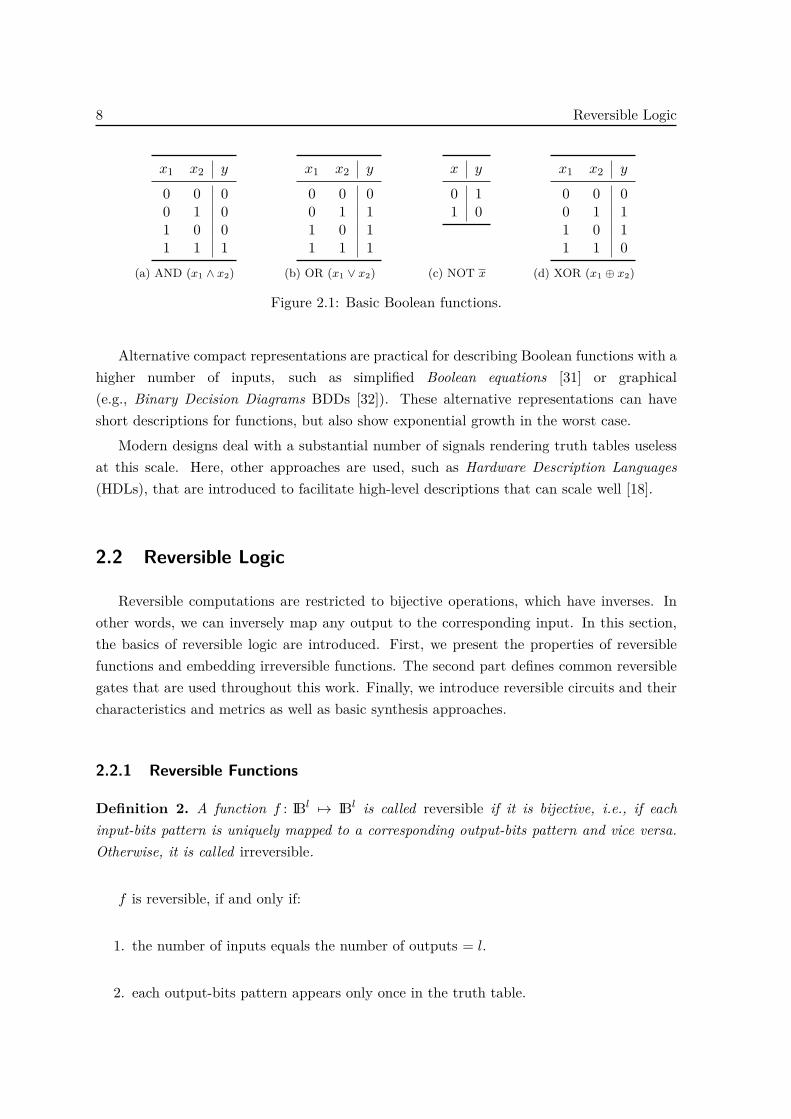
Definition 1. A Boolean function f is a mapping f : IBn 7→ IBm with n inputs andm outputs.
There are 2(m·2n) possible Boolean functions in a system with n-inputs and m-outputs.Elementary functions, such as conjunction (∧,AND), disjunction (∨,OR), negation (¬,NOT),and inequality (⊕,XOR) are combined in Boolean expressions to describe complex functionsfully.
The most straightforward and direct way to specify the behaviour of a Boolean function isby enumerating the output’s response to each input bit-vector. This input/outputrelationship is commonly enumerated in a tabular form, called a truth table, in which allpossible input bit-vectors are listed on the left side of the table, and the correspondingoutput bit-vectors computed by the function are listed on the right side of the table. Forinstance, Figure 2.1 shows truths tables for the basic logical operations. The number ofrows in a truth table equals the number of possible input bit combinations, 2n, where nis the number of inputs. This exponential growth in the sizes of truth tables limits thesemethodologies in a practical sense to functions with only a small number of inputs.
8 Reversible Logic
x1 x2 y
0 0 00 1 01 0 01 1 1
(a) AND (x1 ∧ x2)
x1 x2 y
0 0 00 1 11 0 11 1 1
(b) OR (x1 ∨ x2)
x y
0 11 0
(c) NOT x
x1 x2 y
0 0 00 1 11 0 11 1 0
(d) XOR (x1 ⊕ x2)
Figure 2.1: Basic Boolean functions.
Alternative compact representations are practical for describing Boolean functions with ahigher number of inputs, such as simplified Boolean equations [31] or graphical(e.g., Binary Decision Diagrams BDDs [32]). These alternative representations can haveshort descriptions for functions, but also show exponential growth in the worst case.
Modern designs deal with a substantial number of signals rendering truth tables uselessat this scale. Here, other approaches are used, such as Hardware Description Languages(HDLs), that are introduced to facilitate high-level descriptions that can scale well [18].
2.2 Reversible Logic
Reversible computations are restricted to bijective operations, which have inverses. Inother words, we can inversely map any output to the corresponding input. In this section,the basics of reversible logic are introduced. First, we present the properties of reversiblefunctions and embedding irreversible functions. The second part defines common reversiblegates that are used throughout this work. Finally, we introduce reversible circuits and theircharacteristics and metrics as well as basic synthesis approaches.
2.2.1 Reversible Functions
Definition 2. A function f : IBl 7→ IBl is called reversible if it is bijective, i.e., if eachinput-bits pattern is uniquely mapped to a corresponding output-bits pattern and vice versa.Otherwise, it is called irreversible.
f is reversible, if and only if:
1. the number of inputs equals the number of outputs = l.
2. each output-bits pattern appears only once in the truth table.

2. Reversible Computation 9
x1 x2 x3 y1 y2 y3
0 0 0 0 0 00 0 1 1 0 00 1 0 0 1 00 1 1 0 1 11 0 0 0 1 11 0 1 1 0 11 1 0 1 1 11 1 1 1 1 0(a) f1 : Irreversible function
x1 x2 x3 y1 y2 y3
0 0 0 0 0 00 0 1 0 1 00 1 0 1 0 00 1 1 1 0 11 0 0 0 0 11 0 1 0 1 11 1 0 1 1 01 1 1 1 1 1(b) f2 : Reversible function
Figure 2.2: Examples of Boolean functions.
Example 1. Figure 2.1(c) shows the truth table for a NOT operation. The function isreversible (bijective) because the number of inputs (n = m = 1) and each input-bits patternis uniquely mapped into an output-bits pattern. On the other hand, AND, OR, and XORfunctions (as described in Figure 2.1(a), 2.1(b), and 2.1(d)) are non-reversible because theyhave inputs (n = 2) and outputs (m = 1), i.e., (n 6= m). The function f1 presented inFigure 2.2(a) is also irreversible because the inputs are not uniquely mapped into the outputs(e.g., both inputs 011 and 100 map to the same output 011). In contrast, the function f2
outlined in Figure 2.2(b) is reversible, since each input vector maps to a unique output vectorand the number of inputs is equal to the number of outputs (n = m = 3).
2.2.2 Embedding of Irreversible Functions
An irreversible function can be embedded into a reversible specification by adding extravariables to achieve a bijective function. An embedding is not unique, and the choice ofembedding can have a very significant effect on the number of the variables of the resultingfunction [33,34].
Definition 3. A reversible function g : IB(n+p) 7→ IB(m+k) embeds the irreversiblef : IBn 7→ IBm, if fi(X) = gi(X) for each X ∈ IBn and each i ∈ {1, 2, . . . , m}. Thefunction g is called an embedding and the additional k outputs of g are referred to as garbageoutputs. Furthermore, p additional input variables are added such that (n+p) = (m+k) = l
to obtain a reversible function for the embedding g. The additional p inputs are referred toas constant inputs.
More precisely, given an m-output irreversible function f on n variables, a reversiblefunction g with m + k outputs is determined such that g agrees with f on the first mcomponents. Then, bijectivity can readily be achieved, e.g., by adding p additional inputssuch that f evaluates to its original values in case these inputs are assigned the constant
10 Reversible Logic
Cin x2 x1 Cout S
0 0 0 0 00 0 1 0 10 1 0 0 10 1 1 1 01 0 0 0 11 0 1 1 01 1 0 1 01 1 1 1 1
(a) 1-bit full adder f : IB3 7→ IB2
C Cin x2 x1 Cout S γ1 γ2
0 0 0 0 0 0 0 00 0 0 1 0 1 0 10 0 1 0 0 1 1 00 0 1 1 1 0 1 10 1 0 0 0 1 0 00 1 0 1 1 0 0 10 1 1 0 1 0 1 00 1 1 1 1 1 1 11 0 0 0 1 0 0 01 0 0 1 1 1 0 11 0 1 0 1 1 1 01 0 1 1 0 0 1 11 1 0 0 1 1 0 01 1 0 1 0 0 0 11 1 1 0 0 0 1 01 1 1 1 0 1 1 1
(b) 1-bit full adder embedded in g : IB4 7→ IB4
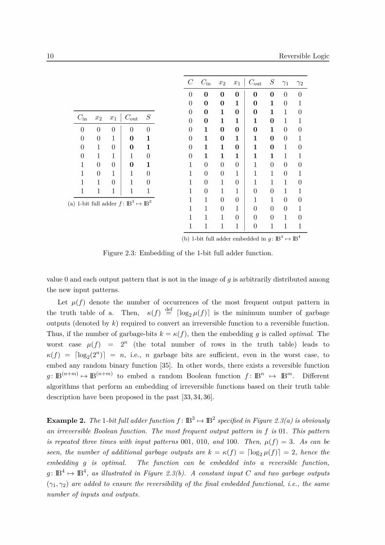
Figure 2.3: Embedding of the 1-bit full adder function.
value 0 and each output pattern that is not in the image of g is arbitrarily distributed amongthe new input patterns.
Let µ(f) denote the number of occurrences of the most frequent output pattern inthe truth table of a. Then, κ(f) def= dlog2 µ(f)e is the minimum number of garbageoutputs (denoted by k) required to convert an irreversible function to a reversible function.Thus, if the number of garbage-bits k = κ(f), then the embedding g is called optimal. Theworst case µ(f) = 2n (the total number of rows in the truth table) leads toκ(f) = dlog2(2n)e = n, i.e., n garbage bits are sufficient, even in the worst case, toembed any random binary function [35]. In other words, there exists a reversible functiong : IB(n+m) 7→ IB(n+m) to embed a random Boolean function f : IBn 7→ IBm. Differentalgorithms that perform an embedding of irreversible functions based on their truth tabledescription have been proposed in the past [33,34,36].
Example 2. The 1-bit full adder function f : IB3 7→ IB2 specified in Figure 2.3(a) is obviouslyan irreversible Boolean function. The most frequent output pattern in f is 01. This patternis repeated three times with input patterns 001, 010, and 100. Then, µ(f) = 3. As can beseen, the number of additional garbage outputs are k = κ(f) = dlog2 µ(f)e = 2, hence theembedding g is optimal. The function can be embedded into a reversible function,g : IB4 7→ IB4, as illustrated in Figure 2.3(b). A constant input C and two garbage outputs(γ1, γ2) are added to ensure the reversibility of the final embedded functional, i.e., the samenumber of inputs and outputs.

2. Reversible Computation 11
X ′ /
xnx1
/ X ′
xn ⊕ g(X ′)x1
x1 ⊕ 1
g
(a) NOT
x1 x1
x2 x2
. .. .. .
xn−1 xn−1
xnx2 xn ⊕ (x1 ∧ · · · ∧ xn−1)x1 x1
x2 ⊕ x1
(b) CNOT
x1 x1
x2 x2
. .. .. .
xn−1 xn−1
xn xn ⊕ (x1 ∧ · · · ∧ xn−1)
(c) MCTFigure 2.4: Toffoli gates.
2.2.3 Reversible Gates
Reversible functions can be realised by reversible circuits in which each variable of thefunction is represented by a circuit line to maintain the bijectivity property of the reversiblefunction. There exist different gate libraries used to build reversible circuits. However, inthe scope of this work, we restrict ourselves to those most commonly used containing theToffoli gate [37] and the Fredkin gate [38]. For this purpose, each gate gi in the circuit isdenoted by g(C, T ) with control lines C ⊂ X and target lines T ⊆ X \ C.
2.2.3.1 Toffoli Gates
A Toffoli gate has one target line T = {xt} and maps the input X = {x1, x2, . . . , xn}:
(x1, . . . , xn) 7→ (x1, . . . , xt−1, xt ⊕∧xj∈C
xj , xt+1, . . . , xn),
i.e., the value on line xt is inverted if and only if all control values are assigned 1. TheToffoli gate is called a NOT if |C| = ∅. Here, the gate maps the single input, such thatx 7→ (x ⊕ 1), i.e., output is unconditionally inverted. On the other hand, a Toffoli gate iscalled a CNOT, or Feynman gate, if it has one control line xc and one target line xt. Here,the gate maps (xc, xt)x 7→ (xc, xt ⊕ xc), while Toffoli gates with more than one controlline are usually referred to as Multiple control Toffoli, MCT, as seen in Figure 2.4. For agraphical representation of Toffoli gates, solid black circles (•) indicate controls and targetlines are denoted with the symbol ⊕.
2.2.3.2 Fredkin Gates
A Fredkin gate has two target lines T = {xs, xt} and maps the input
(x1, . . . , xn) 7→ (x1, . . . , xs−1, x′s, xs+1, . . . , xt−1, x
′t, xt+1, . . . , xn),
with x′s = (ξxs ⊕ ξxt), x′t = (ξxt ⊕ ξxs), and (ξ =∧xj∈C
xj), i.e., the values of the target lines
are interchanged (swapped) if and only if all control values are assigned 1. A Fredkin gateis referred to as a SWAP gate if |C| = ∅. For a graphical representation of Fredkin gates,solid black circles (•) indicate controls and target lines are denoted with the symbol ×, asseen in Figure 2.5(a). Any Fredkin gate can be realised by cascading three Toffoli, as inFigure 2.5(b).

12 Reversible Logic
x1 x1
xn−2 xn−2
. .. .. .
xs x′sxt x′t
××
(a) Symbol
x1 x1
xn−2 xn−2
. .. .. .
xs x′sxt x′t
(b) Toffoli implemetation
Figure 2.5: Fredkin gate.
2.2.4 Reversible Circuits
A reversible circuit is an acyclic combinational logic circuit in which all gates are reversibleand interconnected without explicit fan-outs and loops [39]. Therefore, reversible circuitscan be built as a cascade of reversible gates G = g1 . . . gd. Each gate gi realises a reversiblefunction fi : IBl 7→ IBl. The function realised by the circuit is the composition of the functionsrealised by the gates, i.e., f = f1 ◦f2 ◦ · · · ◦fd. In this circuit paradigm, fan-out and feedbackare not directly allowed.
Example 3. Figure 2.6 shows a reversible circuit combined using Toffoli gates. Threeprimary inputs X = (x1, x2, x3) are mapped to two valid outputs Y = (y1, y2). A constantinput is applied to the circuit. On the other hand, the circuit has two garbage outputs.
x1 −
x2 −
x3 y1
0 y2
Figure 2.6: An example reversible circuit.
By definition, reversible computations are bijective, i.e., for each reversible circuit,G = g1 g2 . . . gd there exists an inverse circuit G−1, such that the cascade G G−1 = I,where I is a unity mapping I : X 7→ X. Toffoli and Fredkin gates are self-inverse gates, i.e.,gi = g−1
i . Consequently, by backward arranging the gates backwards, the inverse circuit iscomputed G−1 = gd gd−1 . . . g1. Hence, for G = G1 G2 the inverse G−1 = G−1
2 G−11 .
Irreversible Boolean functions can be synthesised to a reversible circuit after embeddingthem to reversible functions. Therefore, in general, a reversible circuit contains l lines withn primary inputs and p constant inputs with (n + p) = l. At the output side, there are mprimary outputs and k garbage outputs with (k + m) = l. Figure 2.7 depicts the generalstructure of a reversible circuit inspired from [39]. Note that when the function f is bijective,there are neither constant inputs nor garbage outputs. This follows from [3] where it wasshown that any reversible function f : IBn 7→ IBn could be realised by a reversible circuitwith n lines when using MCT gates. This means that it is not necessary to apply anyconstant input to realise the circuit.

2. Reversible Computation 13
x1
...
xn
0...0
γ1...γk
y1
...
ym
Reversiblecircuit
nPrimaryinputs
pConstant
inputs
kGarbageoutputs
mPrimaryoutputs
Figure 2.7: Reversible circuit structure.
Example 4. Figure 2.8(a) shows a truth table for an embedded AND function (x1∧x2) witha constant input c and two garbage outputs γ1 and γ2. On the other hand, Figure 2.8(b)shows an embedded XOR function (x1 ⊕ x2) where only one garbage γ is required. Here, noconstant input is needed to compute this function (reversible computation).
c x1 x2 y γ1 γ2
0 0 0 0 0 00 0 1 0 0 10 1 0 0 1 00 1 1 1 1 11 0 0 1 0 01 0 1 1 0 11 1 0 1 1 01 1 1 0 1 1
(a) Embedded AND
x1 x2 y γ
0 0 0 00 1 1 11 0 1 01 1 0 1
(b) Embedded XOR
Figure 2.8: Embedded functions.
2.2.5 Metrics of Reversible Circuits
It is important to evaluate the resulting circuits to compare different synthesis approaches.Depending on the target application, different metrics are applied to measure the quality ofa given circuit.
2.2.5.1 Number of Lines
The number of lines l refers to the total number of the input or output variables used ina reversible circuit. If the function to be synthesised is reversible, then the number of circuitlines can be equal to the number of the inputs. However, in the case where the Booleanfunction to be synthesised is irreversible, then additional variables (i.e., constant inputs andgarbage outputs) are unavoidable [36]. For example, the circuit in Figure 2.6 has a totalnumber of lines l = 4, one of which has a constant input, which indicates some irreversiblefunction embedded within the reversible circuit.
14 Reversible Logic
Good circuit realisations try to keep the number of lines as small as possible. Thisis motivated by the fact that, in the domain of quantum computations, each circuit linerepresents a quantum-bit (qubit), which is a very limited resource [40]. Therefore, severaloptimisation approaches that target a reduction of the number of lines in reversible circuitshave been proposed [41].
2.2.5.2 Gate Count
The gate count d refers to the total number of gates in a reversible circuit, e.g., d = 4in Figure 2.6. This metric is used to evaluate a given realisation for a reversible function.However, it is a poor measure of actual reversible circuit complexity because different gatescan have dramatically different complexities depending on the technology used in the physicalimplementation of the circuit. Consequently, minimisation based on this metric does notguarantee a minimum complexity of the physical circuit. In fact, it is possible to reduce theoverall cost using extra gates [42].
2.2.5.3 Technology-dependent Cost Metrics
The complexity of reversible circuits is measured by different cost metrics, which aremore technology dependent, such as quantum costs and transistor costs. The cost CG of areversible circuit G = g1g2 . . . gd is the summation of the costs of the individual gates. i.e.,
CG =d∑i=1
Cgi , where Cgi is the cost of the individual gate gi (the ith in the circuit cascade).
While the transistor cost model estimates the cost of the circuit in terms of the numberof CMOS transistors [43], the quantum cost model estimates the cost of the circuit in termsof the number of elementary quantum gates [14]. Both metrics define the cost of a singleToffoli/Fredkin gate depending on the number of control lines.
• Transistor cost model: The transistor cost of a gate estimates the effort needed torealise a reversible gate in CMOS according to [11] defined to be Cg = (8× n), wheren is the number of control lines in the gate [43]. Then, the transistor cost metric of acircuit is the total sum of transistor costs of all reversible gates in the circuit.
• Quantum cost model: The quantum cost of a Toffoli gate, as introduced in [44] andoptimised in [45], is given in Table2.1, where n denotes the number of control lines forthe gate and l denotes the total number of circuit lines. The quantum cost dependson the number n of control lines as well as the number (l − (n + 1)) of empty linesneither used as a control line nor a target line for the gate. These free-to-use lines arealso called ancilla lines. More empty lines generally lead to cheaper gate realisation,although, for each gate size, there is a minimal cost which is not reduced by havingfurther extra lines available, as outlined in Table 2.1a. On the other hand, the quantumcost of a Fredkin gate with n control lines is computed as the cost of a Toffoli gate ofn+ 1 controls plus the cost of two CNOT gates (see Table 2.1b).
2. Reversible Computation 15
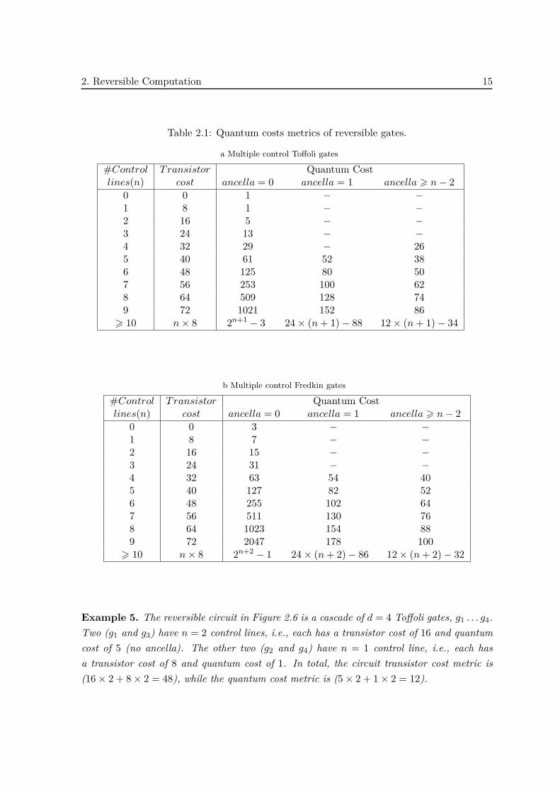
Table 2.1: Quantum costs metrics of reversible gates.
a Multiple control Toffoli gates
#Control Transistor Quantum Costlines(n) cost ancella = 0 ancella = 1 ancella > n− 2
0 0 1 − −1 8 1 − −2 16 5 − −3 24 13 − −4 32 29 − 265 40 61 52 386 48 125 80 507 56 253 100 628 64 509 128 749 72 1021 152 86
> 10 n× 8 2n+1 − 3 24× (n+ 1)− 88 12× (n+ 1)− 34
b Multiple control Fredkin gates
#Control Transistor Quantum Costlines(n) cost ancella = 0 ancella = 1 ancella > n− 2
0 0 3 − −1 8 7 − −2 16 15 − −3 24 31 − −4 32 63 54 405 40 127 82 526 48 255 102 647 56 511 130 768 64 1023 154 889 72 2047 178 100
> 10 n× 8 2n+2 − 1 24× (n+ 2)− 86 12× (n+ 2)− 32
Example 5. The reversible circuit in Figure 2.6 is a cascade of d = 4 Toffoli gates, g1 . . . g4.Two (g1 and g3) have n = 2 control lines, i.e., each has a transistor cost of 16 and quantumcost of 5 (no ancella). The other two (g2 and g4) have n = 1 control line, i.e., each hasa transistor cost of 8 and quantum cost of 1. In total, the circuit transistor cost metric is(16× 2 + 8× 2 = 48), while the quantum cost metric is (5× 2 + 1× 2 = 12).
16 Reversible Circuit Synthesis
2.3 Reversible Circuit Synthesis
Synthesis is an essential phase in the design flow of reversible circuits. The goal is tosynthesise a reversible circuit that computes the desired function efficiently, i.e., with fewercircuit lines and with lower total gate cost. Reversible circuit synthesis is approached fromtwo directions, resulting in two main categories of synthesis, each with its pros and cons. Thefirst category ensures a circuit with a minimal number of lines, as in [3,4,36,46,47,48,49,50].These approaches are truth table-based, so they are limited by a small number of inputs. Thesecond category includes hierarchical approaches that decompose a large function into smallersub-functions, and these approaches make use of additional circuit lines to interconnectthe sub-functions to realise the overall function [24, 51, 52]. In comparison, hierarchicalapproaches offer higher capacity in handling designs with a larger number of input signals,but they can not ensure circuits with minimal lines. Examples from both categories areintroduced in the following.
2.3.1 Truth Table-based Synthesis
Truth table-based approaches realise functions as circuits with a minimum number oflines. Here, the function to be synthesised is embedded and described by a truth table(see Section 2.2.2). The number of lines required to compute the desired outputs is equalto the number of columns on one side of the truth table, i.e., either inputs or outputs(l = (n + p) = (k + m)). Here, lines are ensured to be at a minimum because the constantand garbage bits are also mathematically required for an optimal embedding of the desiredfunction.
The transformation-based synthesis [47] is an example of this category. The idea is totraverse each row of a reversible truth table and match the output bit-vector with the inputbit-vector starting from the least significant bit in the first row, until the most significantbit in the last row. When a mismatched bit is detected, the bit is altered for all rows thathave ′1′s in all bit positions that are ′1′s in the mismatched row. This is what an MCT gategi does when its target line is positioned at the mismatched bit, and it has a control inputat each line with value ′1′ in this row. If the truth table rows are arranged in ascendingorder, then these gates do not alter bits in rows that were previously matched. When thismatching is concluded, the circuit outputs match the inputs, i.e., an identity function isachieved. Hence, gates are appended starting from the output side of the circuit (gd), untilthe last gate becomes the first from the input side (g1), where d is the gate count equalto the number of steps required to match the outputs to the inputs totally. This synthesisapproach results in circuits with a total number of lines n as defined above.
2. Reversible Computation 17
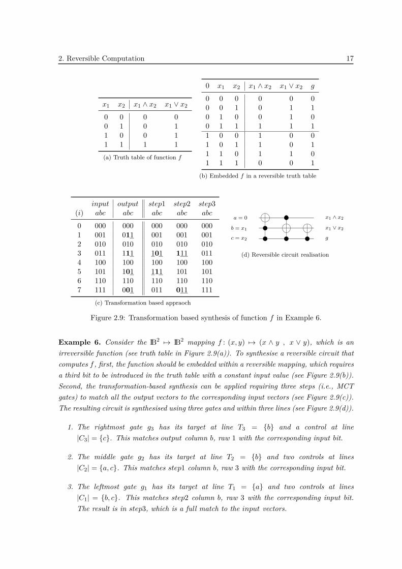
x1 x2 x1 ∧ x2 x1 ∨ x2
0 0 0 00 1 0 11 0 0 11 1 1 1(a) Truth table of function f
0 x1 x2 x1 ∧ x2 x1 ∨ x2 g
0 0 0 0 0 00 0 1 0 1 10 1 0 0 1 00 1 1 1 1 11 0 0 1 0 01 0 1 1 0 11 1 0 1 1 01 1 1 0 0 1
(b) Embedded f in a reversible truth table
input output step1 step2 step3(i) abc abc abc abc abc
0 000 000 000 000 0001 001 011 001 001 0012 010 010 010 010 0103 011 111 101 111 0114 100 100 100 100 1005 101 101 111 101 1016 110 110 110 110 1107 111 001 011 011 111
(c) Transformation based appraoch
a = 0 x1 ∧ x2
b = x1 x1 ∨ x2
c = x2 g
(d) Reversible circuit realisation
Figure 2.9: Transformation based synthesis of function f in Example 6.
Example 6. Consider the IB2 7→ IB2 mapping f : (x, y) 7→ (x ∧ y , x ∨ y), which is anirreversible function (see truth table in Figure 2.9(a)). To synthesise a reversible circuit thatcomputes f , first, the function should be embedded within a reversible mapping, which requiresa third bit to be introduced in the truth table with a constant input value (see Figure 2.9(b)).Second, the transformation-based synthesis can be applied requiring three steps (i.e., MCTgates) to match all the output vectors to the corresponding input vectors (see Figure 2.9(c)).The resulting circuit is synthesised using three gates and within three lines (see Figure 2.9(d)).
1. The rightmost gate g3 has its target at line T3 = {b} and a control at line|C3| = {c}. This matches output column b, raw 1 with the corresponding input bit.
2. The middle gate g2 has its target at line T2 = {b} and two controls at lines|C2| = {a, c}. This matches step1 column b, raw 3 with the corresponding input bit.
3. The leftmost gate g1 has its target at line T1 = {a} and two controls at lines|C1| = {b, c}. This matches step2 column b, raw 3 with the corresponding input bit.The result is in step3, which is a full match to the input vectors.

18 Reversible Circuit Synthesis
This approach requires the complete truth table to be available in memory, so due to anexponential growth in memory this approach practically bounds the capacity to relativelysmall number of inputs (up to 30).
2.3.2 Hierarchical Decomposition Synthesis
Hierarchical synthesis methods have been introduced as an alternative, which does notrequire explicit embedding, but do not guarantee a minimum number of circuit lines. In fact,the lines are often much more than the minimum [20].
The general idea of hierarchical methods is to decompose the desired function f intoa smaller set of functions (sub-functions). This decomposition is repeatedly applied until acircuit is realised for the sub-function or evaluated to a constant. Then, for eachdecomposition, the sub-circuit representing the respective operation can be synthesised.Finally, by composing all sub-circuits, a circuit representing the desired function is realised.
Shannon decomposition of an arbitrary function f(x1, . . . , xi, . . . , xn), is a well-knownexample of hierarchical decomposition, and is given by: f = xi· fH ⊕ xi· fL, wherefL = f(x1, . . . , 0, . . . , xn) and fH = f(x1, . . . , 1, . . . , xn), i.e., the original function with inputxi is substituted by 0 and 1 in fL and fH , respectively. Here, f : IBn 7→ IBn is decomposedto fL : IBn−1 7→ IBn−1 and fH : IBn−1 7→ IBn−1, i.e., each has one input variable lessthan the original function f . In the same way, fL and fH can be decomposed into smallersub-functions. This hierarchical decomposition reduces the problem size to moderate theexponential growth of functions.
Hierarchical function decomposition motivates compelling representations of Booleanfunctions, such as Binary Decision Diagrams (BDD), which are based on graph theory andprovide efficient data-structures that can represent large functions more compactly thantruth tables [32, 53]. BDD-based synthesis has been proposed for larger scale functions inthe reversible circuit paradigm (up to 200 inputs) [52,54,55].
A node (a circle in the graph) represents a function or sub-function with an input-variableidentifier written inside the node. Depending on the value of this input, it decides on either 1referring to the continuous-line edge leads to the sub-function fH , or 0 then the dashed-lineedge leading to the sub-function fL. This completes when it reaches a terminal node withconstant value {0, 1}. BDD-based synthesis traverses this decision-diagram and substituteseach node with a predefined cascade of reversible gates [52].
Example 7. Figure 2.10(a) shows a reduced BDD representation of the function described inthe truth table in Figure 2.9(a). The reversible circuit realised from this approach is computedusing a total of four lines, as shown in Figure 2.10(b), i.e., with one more line comparedto the transformation-based approach. Here, two constant inputs are applied to the circuitinstead of just one line.

2. Reversible Computation 19
x2
x1 x1
0 1
x1 ∧ x2 x1 ∨ x2
(a) BDD of f
0 x1 ∧ x2
0 x1 ∨ x2
x1 x1
x2 x2
(b) Reversible circuit realisation
Figure 2.10: BDD-based synthesis of function f from Example 7.
Examples 6 and 7 describe a simple function. The more complex a function, the moreconstant input lines it exploits to be computed using hierarchical approaches, which is theprimary drawback of this category. Also, obtaining a minimised BDD is not trivial.
As digital systems are rapidly becoming more complex, bit-level descriptions are nolonger suitable to describe them. The hierarchical decomposition concept opens the door formore abstract descriptions, such as Hardware Description Languages, for complex systemsin the conventional circuit paradigm. This high level description allows for modular andscalable designs [56, 57, 58]. Similarly, a dedicated reversible hardware description languageSyReC is proposed to facilitate scalable synthesis of reversible circuits through common HDLmeans [24], and SyReC will be reviewed in Chapter 3.
2.3.3 Trade-off in Circuit Lines and Gate Costs
Here, many synthesis approaches are compared and their characteristics are observed.While minimum line methods result in circuits with fewer lines, often the respectivequantum/transistor costs are higher in comparison to hierarchical synthesis. In contrast,hierarchical approaches need a significant number of additional constant inputs appliedto circuits, but usually with lower quantum costs [20], which shows the complementarycharacteristics of these two categories. Figure 2.11 illustrates the problem with an abstractrelation between the number of lines and the quantum cost to realise function f using differentsynthesis methods. Extreme results appear either with high quantum cost or with largenumber of lines. This motivates investigating possible trade-offs between circuit metrics torealise moderate circuits that are neither extreme in lines nor costs. A trade-off can be madein either direction, i.e., by adding lines to reduce the cost of a minimal lines circuit or byinserting circuitry to avoid (remove) a constant input.

20 Reversible Circuit Synthesis
Number of cirrcuit lines
Qua
ntum
Cos
t
Line reduction
Cost reduction
• Minimum lines
© Possible trade off
• Minimum Cost
Figure 2.11: Gate costs vs. circuit lines.
2.3.3.1 Reducing Gate Cost by Adding Lines
An observation made in [42] is exploited for reducing gate costs. Here, it was observedthat many reversible circuits are composed of cascades of gates with several common controllines. As reviewed in Section 2.2.5.3, the costs of single gates depend on their respectivenumber of control lines. Hence, buffering the results of common control conditions of acascade of gates enables the reduction in the number of required control lines in each gate.As a result, the costs of each gate and the costs of the entire circuit are decreased significantly.
Improvement is only possible if the total costs of the two added gates are less thanthe costs saved by buffering the common control lines. Further, a free ancillary line mustbe available. This is either already the case (e.g., when a constant circuit line is requiredanyway for the realization of other parts in the circuit) or can explicitly be added by thedesigner to enable the reduction.
Following this concept, the cost of a circuit G can be moderated using a helper line asfollows:
1. Determine cascades of gates g1(C1,T1) . . . gk(Ck,Tk) which satisfy the following criteria:
(a) The gates in the cascade have a common set C ′ of control lines, i.e., Ci ⊇ C ′
for 1 ≤ i ≤ k.
(b) The value of the common control lines is not modified within this cascade,i.e., C ′ ∩ gi = ∅ for 1 ≤ i ≤ k.
2. Create a new cascade g0(C′,{h}) g1((C1\C′)∪{h},T1) . . . g1((Ck\C′)∪{h},Tk) gk+1(C′,{h}) .
3. If a free circuit line h is available and the new cascade is cheaper than the originalcascade, then replace the original cascade with the new.

2. Reversible Computation 21
x1 −
x2 −
x3 −
x4 −
x5 f1
x6 f2
x7 f3
(a) Original realisation
h = 0 h = 0x1 −
x2 −
x3 −
x4 −
x5 f1
x6 f2
x7 f3
(b) Revised realisation
Figure 2.12: Cost-aware synthesis.
Example 8. Figure 2.12 demonstrates how the helper line concept is applied to reduce gatecost. Figure 2.12(a) includes a reversible circuit with five gates that has two control linesin common C ′ = {x1, x2}. A constant helper line (h = 0) is applied, and a new Toffoligate is appended at the beginning of the circuit with h as the target and lines C ′ as controls,i.e., g0({x1,x2},h). A similar gate is appended at the end of the circuit to inversely computethe ancillary helper line h, i.e., g6({x1,x2},h). the circuit with the helper line, as shown inFigure 2.12(b), has a quantum cost metric of (Qc = 59) (i.e., low cost) as compared to itsequivalent with no helper line (Figure 2.12(a)), which has a quantum cost of (Qc = 113).
Using helper lines is not limited to just one line as two helper lines may achieve a furtherreduction in the gate cost [42].
2.3.3.2 Reducing Lines
As mentioned in Section 2.3.2, the major drawback associated with hierarchical synthesisapproaches is the high number of circuit lines. Precisely speaking, constant inputs aremassively applied to the circuit to interconnect sub-circuits (sub-functions) together inrealising the overall function.
In such cases, realising circuits with fewer lines is a more critical issue than the costmetrics, where the gate cost increase is justified by reducing the number of circuit lines.Consequently, hierarchical synthesis approaches with line-awareness are required to maintainthe scalability while realising a circuit with fewer lines whenever possible.
The general idea of this optimisation approach exploits special circuit structures oftenoccurring in circuits generated by hierarchical synthesis approaches [59]. Particularly, lineswith constant inputs that end as garbage outputs are considered candidates for thisoptimisation. Since the value of a garbage output does not matter (a ”don’t care” signal),this approach might offer a possibility to merge the line with the constant input producingthe garbage output. If it is possible to modify the circuit so that a garbage output returnsa constant value instead of an arbitrary value, then the line can be reused in the rest of thecircuit. As a result, one constant input line can be removed [60].

22 Summary
Definition 4. Re-computation of a garbage line is made by applying the inverse computationto this line to obtain its initial value (constant input).
It is possible to achieve significant reductions in the overall number of lines byre-computing and reusing lines, which might be applied on the same line more than oncewithin the circuit. Variations of this arrangement are applied in different chapters in thiswork for realising operations with line-awareness.
2.4 Summary
This chapter provides a brief introduction of the necessary background on reversiblecircuits.
A reversible Boolean function is a bijection, i.e., a mapping where the output is uniquelydetermined from input and the vice versa. To satisfy this, (1) the number of input-bitsshould be equal to the number of output-bits, and (2) no output pattern is repeated in thetruth table.
Irreversible functions can be embedded within reversible functions. This embeddingrequires additional bits to be added to the output pattern (garbage), such that no patternis repeated. This garbage implies adding constant bits to the input side to make the totalnumber of inputs equal to the total number of outputs. The embedding is optimal if onlythe mathematically necessary number of garbage outputs are used.
The conventional elementary gates, such as AND and, OR are not reversible. In thereversible computational paradigm, another set of gates are defined, and in this work, thereversible Toffoli and Fredkin gates are used.
Reversible circuits are cascades of reversible gates that are combined to compute certainfunctions. Neither feed-backs nor fan-outs are allowed directly in the reversible circuitparadigm. A circuit inverse computes the inverse function and is realised simply by reversingthe order of the gates in the cascade.
The quality of a reversible circuit is measured using the number of lines as well as the totalgate cost. The cost is measured either by the gate count, the transistor cost or the quantumcost. Circuit metrics (lines and cost) are shown to be trade-offs as there exist arrangementsto reduce the gate cost by adding lines, and other arrangements that add gates (i.e., extracost) to reduce some lines from the circuits.
Reversible circuit synthesis approaches are categorized into; (1) minimal line approaches,which result in fewer lines but high costs, and (2) hierarchical (decomposition) approaches,which have higher scalability but result in circuits with more lines. HDL-based synthesis is ahierarchical approach that offers high scalability in conventional as well as reversible circuitdesign.

23
Chapter 3
SyReC Specification and Synthesis ofReversible Circuits
SyReC is a dedicated reversible hardware description language that facilitates scalablesynthesis through common HDL means. It allows for the specification and automaticsynthesis of complex reversible circuits. SyReC was first reported in [61] to specify reversiblecircuits at a higher level of abstraction, in particular for the design of complex functionality,such as a RISC CPU [25]. For such designs, SyReC outperforms currently applied descriptionmeans, including truth tables, permutations, and decision diagrams.
Hierarchical approaches to reversible circuit synthesis, including SyReC, typically resultin circuits with a large number of lines. This sever drawback highlights the need forline-aware synthesis, which is tackled with a revised SyReC-based synthesis configured torealise the desired circuit with fewer lines [62]. Despite being less critical for this approach,the cost-aware configuration has also been proposed to reduce the gate cost associated withcertain cases [24].
In this chapter, we introduce the SyReC as the state-of-the-art and cover in detail generalconcepts, specification syntax and semantics, its special hardware related properties andconstraints, and the synthesis of SyReC specifications. 1
3.1 SyReC: The Language
Since all (valid) SyReC programs are inherently reversible, the reversibility of thespecification is simultaneously ensured. The general concepts to achieve this are summarisedin the first part of this section followed by an explanation of the syntax and semantics of allSyReC description means.
1 Comprehensive reviews with additional details on SyReC are found in [24,63].

24 SyReC: The Language
3.1.1 General Concepts
To ensure reversibility in its description, SyReC adapts established concepts from thepreviously introduced reversible programming language, Janus [64], and is additionallymodified by hardware-related language constructs since it targets the description of reversiblecircuits. The
1. Reversible Assignments: Being one of the most elementary language constructs,variable assignments, such as those used in most imperative languages, are irreversibleand cannot be part of a reversible language. The concept of reversible assignments (alsocalled reversible updates) is used as an alternative. Reversible assignments have theform v ⊕ = e with ⊕ ∈ {ˆ, +, -} such that the variable v does not appear on theright-hand side expression e. Although SyReC is limited to the set of operators in ⊕,any operator f can be used for the reversible assignment if there exists an inverseoperator f−1 such that
v = f−1(f(v, e), e) (3.1)
for all variables v and all expressions e. Note that ‘+’ (addition) is inverse to‘-’ (subtraction) and vice versa, and ‘ˆ’ (bit-wise exclusive OR) is inverse to itself.When executing the program in reverse order, all reversible assignment operators arereplaced by their inverse operators.
2. Expressiveness: Due to the construction of the reversible assignment, the right-handside expression can also be irreversible and compute any operation. The most commonoperations are directly applicable using a wide variety of syntax, including arithmetic(+, *, /, %, *>), bit-wise (&, |, ˆ), logical (&&, ||), and relational (<, >, =, !=, <=,>=) operations. The reversibility is ensured, since the input values to the operation arealso given to the inverse operation when reverting the assignment (see Equation (3.1)).For example, to specify a multiplication a*b, a new free signal c must be introduced tostore the result, i.e., cˆ=(a*b) is applied.
3. Reversible Control Flow A reversible data flow is ensured due to the assignmentoperation mentioned above, and the control flow is made bijectively executable in asimilar fashion. This becomes particularly manifest in conditional statements. Incontrast to non-reversible languages, SyReC requires an additional fi-condition foreach if -condition which is applied as an assertion. This fi-condition is required, sincea conditional statement may not be computed in both directions using the samecondition, i.e., it cannot be ensured that the same block (then-block or else-block)is processed when computing an if -statement in the reverse direction. As a solution, acorrected fi-condition asserted when computing the statement in the reverse direction isadded to ensure a consistent execution semantic. This language principle is illustratedin detail in the next section.

3. SyReC Specification and Synthesis of Reversible Circuits 25
4. Hardware Description Properties: Since SyReC is used for the synthesis ofreversible circuits, it obeys some HDL related properties:
• The single data-type is a circuit signal with parameterised bit-width.
• Access to single bits (x.N), a range of bits (x.N:N), and the size (#x) of a signalis provided.
• Since loops must be completely unrolled during synthesis, the number of iterationshas to be available before compilation. So, dynamic loops (defined by expressions)are not allowed.
• Additional operations used in hardware design (e.g., shifts ‘<<’ and ‘>>’) areprovided.
The implementation of these general concepts for the SyReC syntax is illustrated indetail using the EBNF in Figure 3.1.
Table 3.1: Signal access modifiers and implied circuit properties.
Modifier Constant Garbage State InitialInput Output Value
in – yes no given by primary inputout 0 no no 0inout – no no given by primary inputwire 0 yes no 0state – no yes given by pseudo-primary input
3.1.2 Module and Signal Declarations
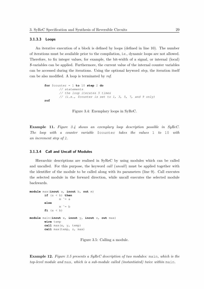
Each SyReC specification (denoted by 〈program〉 in line 1 in Figure 3.1) consists of oneor more modules (denoted by 〈module〉 in line 2). A module is introduced with the keywordmodule and includes an identifier (represented by a string as defined in line 23), a list ofparameters representing global signals (denoted by 〈parameter− list〉 in line 3), local signaldeclarations (denoted by 〈signal − list〉 in line 5), and a sequence of statements (denotedby 〈statement − list〉 in line 7). The top-module of a program is defined by the specialidentifier main. If no module with this name exists, the last module declared is used as thetop-module instead.
SyReC uses a signal representing a non-negative integer as its sole data type. Roundbrackets can optionally define the bit-width of signals after the signal name (line 6). If nobit-width is specified, a default value of 32-bit is assumed. For each signal, an access modifiermust be defined. For a parameter signal (used in a module declaration), this can be eitherin, out, or inout (line 4).

26 SyReC: The Language
Program and Modules
〈program〉 ::= 〈module〉 {〈module〉} 〈module〉 ::= ‘module’ 〈identifier〉 ‘(’ [〈parameter-list〉] ‘)’ {〈signal-list〉}
〈statement-list〉 〈parameter-list〉 ::= 〈parameter〉 {‘,’ 〈parameter〉} 〈parameter〉 ::= (‘in’ | ‘out’ | ‘inout’) 〈signal-declaration〉 〈signal-list〉 ::= (‘wire’ | ‘state’) 〈signal-declaration〉 {‘,’ 〈signal-declaration〉} 〈signal-declaration〉 ::= 〈identifier〉 {‘[’〈int〉‘]’} [‘(’〈int〉‘)’]
Statements
〈statement-list〉 ::= 〈statement〉 {‘;’ 〈statement〉} 〈statement〉 ::= 〈call-statement〉 | 〈for-statement〉 | 〈if-statement〉 | 〈unary-statement〉 |
〈assign-statement〉 | 〈swap-statement〉 | 〈skip-statement〉 〈call-statement〉 ::= (‘call’ | ‘uncall’) 〈identifier〉 ‘(’ (〈identifier〉 {‘,’ 〈identifier〉}) ‘)’
〈for-statement〉 ::= ‘for’ [[‘$’ 〈identifier〉 ‘=’] 〈number〉 ‘to’] 〈number〉 [‘step’ [‘-’]〈number〉] 〈statement-list〉 ‘rof’
〈if-statement〉 ::= ‘if ’ 〈expression〉 ‘then’ 〈statement-list〉 ‘else’ 〈statement-list〉 ‘fi’〈expression〉
〈assign-statement〉 ::= 〈signal〉 (‘ˆ’ | ‘+’ | ‘-’) ‘=’ 〈expression〉 〈unary-statement〉 ::= (‘˜’ | ‘++’ | ‘--’) ‘=’ 〈signal〉 〈swap-statement〉 ::= 〈signal〉 ‘<=>’ 〈signal〉 〈skip-statement〉 ::= ‘skip’
〈signal〉 ::= 〈identifier〉 {‘[’ 〈expression〉 ‘]’} [‘.’ 〈number〉 [‘:’ 〈number〉]]
Expressions
〈expression〉 ::= 〈number〉 | 〈signal〉 | 〈binary-expression〉 | 〈unary-expression〉 |〈shift-expression〉
〈binary-expression〉 ::= ‘(’ 〈expression〉 (‘+’ | ‘-’ | ‘ˆ’ | ‘*’ | ‘/’ | ‘%’ | ‘*>’ | ‘&&’ |‘||’ | ‘&’ | ‘|’ | ‘<’ | ‘>’ | ‘=’ | ‘!=’ | ‘<=’ | ‘>=’) 〈expression〉 ‘)’
〈unary-expression〉 ::= (‘!’ | ‘˜’) 〈expression〉 〈shift-expression〉 ::= ‘(’ 〈expression〉 (‘<<’ | ‘>>’) 〈number〉 ‘)’
Identifier and Constants
〈letter〉 ::= (‘A’ | . . . | ‘Z’ | ‘a’ | . . . | ‘z’)
〈digit〉 ::= (‘0’ | . . . | ‘9’)
〈identifier〉 ::= (‘ ’ | 〈letter〉) {(‘ ’ | 〈letter〉 | 〈digit〉)} 〈int〉 ::= 〈digit〉 {〈digit〉} 〈number〉 ::= 〈int〉 | ‘#’ 〈identifier〉 | ‘$’ 〈identifier〉 | (‘(’ 〈number〉 (‘+’ | ‘-’ | ‘*’ |
‘/’) 〈number〉 ‘)’)
Figure 3.1: Syntax of the hardware description language SyReC.

3. SyReC Specification and Synthesis of Reversible Circuits 27
Local signals can either work as internal signals (denoted by wire) or, in the case ofsequential circuits as state signals2 (denoted by state; line 5). The access modifier affectsproperties in the synthesised circuits as summarized in Table 3.1. Signals can be groupedinto multi-dimensional arrays of constant length using square brackets after the signal nameand before the optional bit-width declaration (line 6).
Example 9. Figure 3.2 shows an exemplary module (myCircuit) declaration possible inSyReC, including one in signal (a) with a single bit, a four-element array of inout signals(x) each with 16 bit-width and an out signal (y) with a default bit-width (32 bit). Also, aninternal signal (wire) (auxSignal) is declared with 16 bits and as well as a state signal(stateSignal) with a default bit-width of 32 bit.
module myCircuit(in opr (1), inout x [4] (16), out y)wire auxSignal(16)state stateSignal
Figure 3.2: Exemplary module and internal signal and state declarations.
3.1.3 Statements
Statements include call and uncall of other modules, loops, conditional statements, andvarious data operations (i.e., reversible assignment operations, unary operations, and swapstatements as in line 8). The empty statement can explicitly be modelled using the skipkeyword (line 15). Statements are separated by semicolons (line 7). Signals within statementsare denoted by 〈signal〉 allowing access to the entire signal (e.g., x), a certain bit (e.g., x.4),or a range of bits (e.g., x.2:4 as in line 16). The bit-width of a signal can also be accessed(e.g., #x as in line 25).
3.1.3.1 Signal Update Statements
Reversible signal update statements include the reversible signal assignment(denoted by〈assign− statement〉), unary statements (denoted by 〈unary − statement〉), and the swapstatement (denoted by 〈swap − statement〉) as defined in line 12 to 14. The semantics ofthese statements are summarised in Table 3.2, whereby x, y denote signals and e denotesexpressions. Since these statements perform only reversible operations, they may assign newvalues to signals. Therefore, the respective signal(s) to be modified must not appear in theexpression on the right-hand side.
2Note that depending on the application feedback, the corresponding state signals might not be allowedin reversible circuits. Nevertheless, SyReC supports this concept in principle. For a detailed discussion onreversible sequential circuits, refer to [65,66].
28 SyReC: The Language
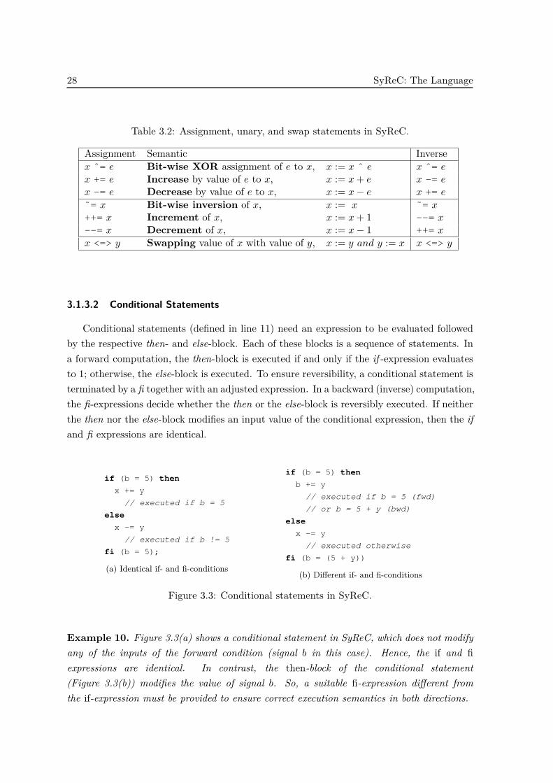
Table 3.2: Assignment, unary, and swap statements in SyReC.
Assignment Semantic Inversex ˆ= e Bit-wise XOR assignment of e to x, x := x ˆ e x ˆ= ex += e Increase by value of e to x, x := x+ e x -= ex -= e Decrease by value of e to x, x := x− e x += e˜= x Bit-wise inversion of x, x := x ˜= x++= x Increment of x, x := x+ 1 --= x--= x Decrement of x, x := x− 1 ++= xx <=> y Swapping value of x with value of y, x := y and y := x x <=> y
3.1.3.2 Conditional Statements
Conditional statements (defined in line 11) need an expression to be evaluated followedby the respective then- and else-block. Each of these blocks is a sequence of statements. Ina forward computation, the then-block is executed if and only if the if -expression evaluatesto 1; otherwise, the else-block is executed. To ensure reversibility, a conditional statement isterminated by a fi together with an adjusted expression. In a backward (inverse) computation,the fi-expressions decide whether the then or the else-block is reversibly executed. If neitherthe then nor the else-block modifies an input value of the conditional expression, then the ifand fi expressions are identical.
if (b = 5) then
x += y
// executed if b = 5
else
x -= y
// executed if b != 5
fi (b = 5);
(a) Identical if- and fi-conditions
if (b = 5) then
b += y
// executed if b = 5 (fwd)
// or b = 5 + y (bwd)
else
x -= y
// executed otherwise
fi (b = (5 + y))
(b) Different if- and fi-conditions
Figure 3.3: Conditional statements in SyReC.
Example 10. Figure 3.3(a) shows a conditional statement in SyReC, which does not modifyany of the inputs of the forward condition (signal b in this case). Hence, the if and fiexpressions are identical. In contrast, the then-block of the conditional statement(Figure 3.3(b)) modifies the value of signal b. So, a suitable fi-expression different fromthe if-expression must be provided to ensure correct execution semantics in both directions.
3. SyReC Specification and Synthesis of Reversible Circuits 29
3.1.3.3 Loops
An iterative execution of a block is defined by loops (defined in line 10). The numberof iterations must be available prior to the compilation, i.e., dynamic loops are not allowed.Therefore, to fix integer values, for example, the bit-width of a signal, or internal (local)$-variables can be applied. Furthermore, the current value of the internal counter variablescan be accessed during the iterations. Using the optional keyword step, the iteration itselfcan be also modified. A loop is terminated by rof.
for $counter = 1 to 10 step 2 do// statements// the loop iterates 5 times// (i.e., $counter is set to 1, 3, 5, 7, and 9 only)
rof
Figure 3.4: Exemplary loops in SyReC.
Example 11. Figure 3.4 shows an exemplary loop description possible in SyReC.The loop with a counter variable $counter takes the values 1 to 10 withan increment step of 2.
3.1.3.4 Call and Uncall of Modules
Hierarchic descriptions are realised in SyReC by using modules which can be calledand uncalled. For this purpose, the keyword call (uncall) must be applied together withthe identifier of the module to be called along with its parameters (line 9). Call executesthe selected module in the forward direction, while uncall executes the selected modulebackwards.
module max(inout a, inout b, out m)if (a < b) then
m ˆ= aelse
m ˆ= bfi (a < b)
module main(inout x, inout y, inout z, out max)wire tempcall max(x, y, temp)call max(temp, z, max)
Figure 3.5: Calling a module.
Example 12. Figure 3.5 presents a SyReC description of two modules: main, which is thetop-level module and max, which is a sub-module called (instantiated) twice within main.

30 SyReC: The Language
3.1.4 Expressions
Expressions, as defined in lines 17 to 20, are applied on the right-hand side of assignmentstatements or as branching conditions in if and fi statements. Since expressions do notmodify the values of any signal, non-reversible operations can also be applied in expressionswithout jeopardising the reversibility. Because of this, a wide range of different descriptionmeans is provided. Table 3.3 lists the semantics for all operations which can be used inexpressions, whereby e, f denote sub-expressions and N denotes natural numbers.
Table 3.3: Expressions in SyReC.
Operation Semantice + f Addition of e and fe - f Subtraction of e and fe * f Lower bits of multiplication of e and fe *> f Upper bits of multiplication of e and fe / f Division of e and fe % f Remainder of division of e and f
e ˆ f Bit-wise XOR of e and fe & f Bit-wise AND of e and fe | f Bit-wise OR of e and f˜e Bit-wise inversion of ee && f Logical AND of e and fe || f Logical OR of e and f!e Logical NOT of ee < f True, if and only if e is less than fe > f True, if and only if e is greater than fe = f True, if and only if e equals fe != f True, if and only if e not equals fe <= f True, if and only if e is less or equal to fe >= f True, if and only if e is greater or equal to fe << N Logical left shift of e by Ne >> N Logical right shift of e by N
c ˆ= (a * b); // c := a*b if c is a new free signalx.0 ˆ= ((a > 3) && (b != 0));x.1:3 ˆ= (c.0:2 | 4);if (a = b) then c+= (a % 2) else c -= (b / 2) fi (a = b)
Figure 3.6: Application of expressions.
Example 13. Figure 3.6 shows statements for expressions that demonstrate the range ofdescription means available in SyReC. Although the language is restricted to ensurereversibility (e.g., statements such as c = a * b are not allowed), common functionalitycan easily be specified (e.g., with a new free signal c, such as c ˆ= (a * b) ). Despite theusage of non-reversible operations in Figure 3.6, all statements still can be executed in bothdirections.

3. SyReC Specification and Synthesis of Reversible Circuits 31
3.2 Synthesis of SyReC Specifications
In SyReC, it is possible to specify reversible circuits on a higher level of abstraction. Forthe design of complex functionality, SyReC clearly outperforms currently applied descriptionmeans, such as truth tables, permutations, and decision diagrams. The next step is to realiseSyReC specifications as reversible circuits.
To synthesise a given SyReC specification, a hierarchical synthesis method is developed.Existing realisations, so-called building blocks, of the individual statements and expressions,are used and combined so that the desired circuit is realised. More precisely, SyReC synthesis(1) traverses the entire program and (2) adds cascades of reversible gates to the circuitrealising each statement or expression.
Modules are synthesised independently of each other and afterwards cascaded accordingto the respective call and uncall statements. All signals are realised by buses of commonreversible circuit lines with the specified bit-width. In the following, the individual mappingsof the statements to the respective reversible cascades are described. We distinguish betweenthe synthesis of assignment statements (including unary and swap statements), expressions,and control logic including call and uncall, loops, and conditional statements.
3.2.1 Synthesis of Assignment Statements
As introduced in Section 3.1.3.1, assignment statements in SyReC must be reversible. Asa consequence, signal values are not overwritten but rather updated with a new value suchthat the old value can still be recovered by applying the inverted assignment operation. Thenotation, as depicted in Figure 3.7(a), denotes such operations in circuit structures. Solidlines that cross the box represent the signals(s) on the right-hand side of the statement,i.e., the signal(s) whose values are preserved.
The most straightforward reversible assignment operation is the bit-wise XOR (e.g., aˆ=b).For 1-bit signals, this operation can be synthesised by a single Toffoli gate, as shown inFigure 3.7(b). If signals with a bit-width greater than 1 are applied, for each bit a Toffoligate is applied analogously.
To synthesise the increase operation (a += b), a modified addition network is added.In the past, several reversible circuit realisations for addition were investigated, and it iswell known that the minimal realisation of a 1-bit adder consists of four Toffoli gates [67].Thus, cascading the required number of 1-bit adders is a possible realisation. However,since every 1-bit adder also requires one constant input, this is a poor solution with respectto circuit lines. In contrast, heuristic realisations exist that require a fewer number ofadditional lines [68]. Since the increase operation, unlike addition, is reversible, it can evenbe synthesised without additional lines. Such a realisation is used in our approach. Acorresponding cascade for a 3-bit increase is depicted in Figure 3.7(d).
The mapping for the decrease operation (a -= b) is the inverse of the increase operation.So, the same realisation depicted in Figure 3.7(d) is used in reverse.
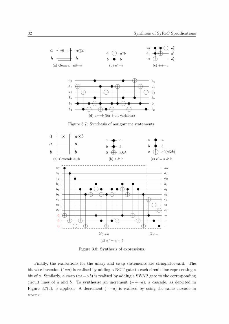
32 Synthesis of SyReC Specifications
a a⊕b⊕=b b
(a) General: a⊕=b
a aˆbb b
(b) aˆ=b
a0 a′0a1 a′1a2 a′2
(c) ++=a
a0 a′0a1 a′1a2 a′2
b0 b0
b1 b1
b2 b2
(d) a+=b (for 3-bit variables)
Figure 3.7: Synthesis of assignment statements.
0 a�b�a a
b b
(a) General: a�b
a a
b b
0 a&b(b) a & b
a a
b b
c cˆ(a&b)
(c) cˆ= a & b
a0 a0
a1 a1
a2 a2
b0 b0
b1 b1
b2 b2
c0 c0
c1 c1
c2 c2
0 −0 −0 −
G(a+b) Gc∧=
(d) c ˆ= a + b
Figure 3.8: Synthesis of expressions.
Finally, the realisations for the unary and swap statements are straightforward. Thebit-wise inversion (˜=a) is realised by adding a NOT gate to each circuit line representing abit of a. Similarly, a swap (a<=>b) is realised by adding a SWAP gate to the correspondingcircuit lines of a and b. To synthesise an increment (++=a), a cascade, as depicted inFigure 3.7(c), is applied. A decrement (- -=a) is realised by using the same cascade inreverse.
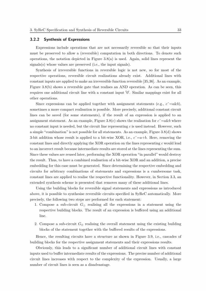
3. SyReC Specification and Synthesis of Reversible Circuits 33
3.2.2 Synthesis of Expressions
Expressions include operations that are not necessarily reversible so that their inputsmust be preserved to allow a (reversible) computation in both directions. To denote suchoperations, the notation depicted in Figure 3.8(a) is used. Again, solid lines represent thesignals(s) whose values are preserved (i.e., the input signals).
Synthesis of irreversible functions in reversible logic is not new, so for most of therespective operations, reversible circuit realizations already exist. Additional lines withconstant inputs are applied to make an irreversible function reversible [35,36]. As an example,Figure 3.8(b) shows a reversible gate that realises an AND operation. As can be seen, thisrequires one additional circuit line with a constant input ′0′. Similar mappings exist for allother operations.
Since expressions can be applied together with assignment statements (e.g., cˆ=a&b),sometimes a more compact realisation is possible. More precisely, additional constant circuitlines can be saved (for some statements), if the result of an expression is applied to anassignment statement. As an example, Figure 3.8(c) shows the realisation for cˆ=a&b whereno constant input is needed, but the circuit line representing c is used instead. However, sucha simple “combination” is not possible for all statements. As an example, Figure 3.8(d) shows3-bit addition whose result is applied to a bit-wise XOR, i.e., cˆ=a+b. Here, removing theconstant lines and directly applying the XOR operation on the lines representing c would leadto an incorrect result because intermediate results are stored at the lines representing the sum.Since these values are reused later, performing the XOR operation “in parallel” would destroythe result. Thus, to have a combined realisation of a bit-wise XOR and an addition, a preciseembedding for this case must be generated. Since determining the respective embedding andcircuits for arbitrary combinations of statements and expressions is a cumbersome task,constant lines are applied to realise the respective functionality. However, in Section 3.3, anextended synthesis scheme is presented that removes many of these additional lines.
Using the building blocks for reversible signal statements and expressions as introducedabove, it is possible to synthesise reversible circuits specified in SyReC automatically. Moreprecisely, the following two steps are performed for each statement:
1. Compose a sub-circuit G� realising all the expressions in a statement using therespective building blocks. The result of an expression is buffered using an additionalline.
2. Compose a sub-circuit G⊕ realising the overall statement using the existing buildingblocks of the statement together with the buffered results of the expressions.
Hence, the resulting circuits have a structure as shown in Figure 3.9, i.e., cascades ofbuilding blocks for the respective assignment statements and their expressions results.
Obviously, this leads to a significant number of additional circuit lines with constantinputs used to buffer intermediate results of the expressions. The precise number of additionalcircuit lines increases with respect to the complexity of the expression. Usually, a largenumber of circuit lines is seen as a disadvantage.

34 Synthesis of SyReC Specifications
a a⊕(b�c)⊕=
0 −Gb�c
b b
c c
d d⊕(e�f)⊕=
0 −Ge�f
e e
f f
Figure 3.9: Resulting circuit structure.
if e
then
a ⊕= b
else
c ⊕= d
fi e
(a) Code
a a′⊕=b b
e −
c c′⊕=d d
(b) Circuit realization
Figure 3.10: Synthesis of conditional statements.
3.2.3 Synthesis of the Control Logic
Finally, the synthesis of control logic is considered. Module calls, uncalls, and loopsare realised straightforwardly. Loops are realized by simply cascading (i.e., unrolling) therespective statements within a loop block for each iteration. Since the number of iterationsmust be fixed (see Section 3.1.3.3), this results in a finite number of statements subsequentlyprocessed. Call and uncall of modules are handled similarly where the respective statementsin the modules are cascaded.
To realise conditional statements, such as if -statements as introduced in Section 3.1.3.2,the statements in the then- and else-block are mapped to reversible cascades with anadditional control line added to all gates (see Figure 3.10(b)). Thus, the respective operationsof the statements in the then or (else-block are computed if and only if the result of theexpression (stored in signal e) is 1 or 0, respectively. A NOT gate is applied to flip the valueof e so that the gates of the else-block can also be “controlled”.

3. SyReC Specification and Synthesis of Reversible Circuits 35
3.3 Circuit Optimization
Hierarchical synthesis approaches do not guarantee optimal circuits, which keeps a spaceopened for refinement. Both circuit trade-off metrics may be considered as optimisationobjectives.
3.3.1 Line-aware Synthesis of SyReC Specifications
To realise SyReC specifications with a smaller number of additional circuit lines, anextended synthesis scheme is presented in this section (based on [62]). The idea is to usethe same building blocks as introduced in the previous section but to undo intermediateresults of the expressions as soon as they are no longer needed. A similar idea (for reversiblesoftware programs) was previously proposed in [69], which enables that reuse of circuit lineswhich previously occupied by expressions.
In the following, the concept of this scheme is illustrated before the extended synthesisis described in detail for all possible SyReC statements. Next, the necessary amount ofadditional circuit lines is discussed.
3.3.1.1 General Concept
The extended synthesis approach follows the scheme as introduced in Section 3.2.2, butis extended by an additional third step:
3. Add the inverse circuit from Step 1,G−1� , to the circuit to reset the circuit lines buffering
the result of the expressions to the constant ′0′.
Example 14. Consider the two following generic HDL statements:
a ⊕= (b � c);
d ⊕= (e � f);
Figure 3.11 sketches the resulting circuit after applying the extended synthesis scheme. Thefirst two sub-circuits Gb�c and Ga⊕=b�c, ensure that the first statement is realised. This isequivalent to the scheme proposed in Section 3.2 and leads to additional lines with constantinputs (highlighted thick). Afterwards, a further sub-circuit, G−1
b�c, is applied. Since G−1b�c
is the inverse of Gb�c, this sets the circuit lines buffering the result of b � c back to theconstant ′0′. As a result, these circuit lines can be reused to realise the following statementsas illustrated for d⊕=e� f in Figure 3.11.
3.3.1.2 Resulting Synthesis Scheme
Following the proposed concept, each statement can be realised with zero garbage outputs.In the following, the precise realisation of this scheme is detailed for each possibly affectedstatement. The unary statements, the swap-statement (<=>), and the skip statement are notconsidered here as they are realised without additional circuit lines.

36 Circuit Optimization
a a⊕(b�c)⊕=0 Gb�c G−1
b�c
b b
c c
d d⊕(e�f)⊕=0 0Ge�f G−1
e�f
e e
f f
Figure 3.11: Line reduction.
Assignment Statements To realise statements of the form a⊕=e with e being an arbitraryexpression, the respective building blocks are orchestrated as illustrated in Figure 3.11. First,a sub-circuit realising the expression e, i.e., the right-hand side of the statement, is created.This requires additional lines to store the result of e. Next, a sub-circuit realising theassignment operation is created as well as a sub-circuit reversing the result of e into aconstant value. The latter is done by reversing the order of gates of the first sub-circuit.Finally, all three sub-circuits are composed leading to the desired realisation of the statement.
Example 15. Figure 3.12 shows the circuit obtained by synthesising cˆ=(a + b) using theextended synthesis scheme. Dashed rectangles highlight the respective sub-circuits Ga+b,Gcˆ=a+b, and G−1
a+b. Since all gates considered in this work are self-inverse, G−1a+b is obtained
by reversing the order of the gates of Ga+b. The target signal is updated exactly as inFigure 3.8(d), but here the three garbage lines are re-computed to the constant ′0′.
a0 a0
a1 a1
a2 a2
b0 b0b1 b1b2 b2c0 c0c1 c1c2 c2
0 00 00 0
G(a+b) Gc∧= G−1(a+b)
Figure 3.12: Synthesizing c ˆ= (a+b) with no garbage.
Applying this procedure, any arbitrary combination of assignment statements andexpressions can be realised in a line-aware manner. That is, required additional circuitlines are ancilla lines and can be reused for other statements and operations.

3. SyReC Specification and Synthesis of Reversible Circuits 37
Conditional Statements
As described in Section 3.2.3, conditional statements are realised by combining twosub-circuits, Gthen and Gelse (see Figure 3.10). Figure 3.13(b) illustrates the adjustedprocedure for the synthesis of a conditional statement in the line-aware configuration ofcircuits. The gates needed to realise the then-block (else-block) are highlighted in dark grey(light grey). Also, a sub-circuit Gif evaluating the respective if -expression is created. Theintermediate results of that expression are handled analogously to assignment statementsas described above. An additional circuit line is applied to store the Boolean result ofthe if -expression and control the execution of the then- and else-block as described inSection 3.2.3. The flip on the additional line, which controls the gates of the else-block,is then restored by another NOT gate. Afterwards, the original constant value of that lineis restored by applying a sub-circuit Gfi which evaluates the fi-expression of the statement.As defined in Section 3.1.3.2, SyReC requires the definition of a fi-expression that evaluatesto the same Boolean value as the if -expression did in Gif .
if (a = b)then
a ⊕= c
else
b ⊕= c
fi (a = (b⊕ c))
(a) Code
0 0Gif Gfi
a a′⊕=
b b′⊕=
c c
(b) Without additional lines
Figure 3.13: Realisation of a conditional statement in line-aware SyReC synthesis.
Loops and Calls
The realisation of loops and module calls is treated in a straight forward manner exploitingthe procedures proposed above. Calls are substituted by the corresponding statements insidethe body of the call. Loops are realised by explicitly cascading (i.e., unrolling) the respectivestatements within a loop block according to the fixed and finite number of iterations.
3.3.1.3 Discussion
Applying the extended synthesis scheme, every statement is synthesised with zero garbageoutputs and only additional ancilla lines. Consequently, the total number of additional linesrequired to realize a SyReC specification with the proposed solution can be determined bythe statement that requires the largest number of additional lines to buffer intermediateresults.
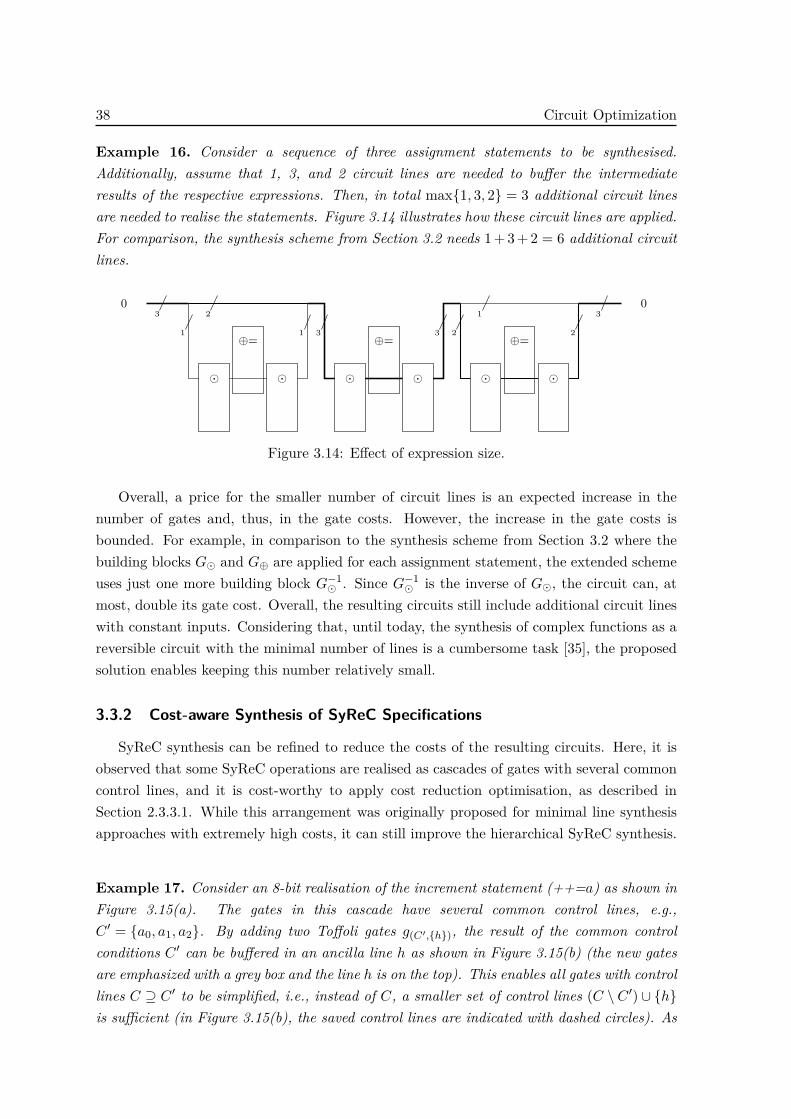
38 Circuit Optimization
Example 16. Consider a sequence of three assignment statements to be synthesised.Additionally, assume that 1, 3, and 2 circuit lines are needed to buffer the intermediateresults of the respective expressions. Then, in total max{1, 3, 2} = 3 additional circuit linesare needed to realise the statements. Figure 3.14 illustrates how these circuit lines are applied.For comparison, the synthesis scheme from Section 3.2 needs 1 + 3 + 2 = 6 additional circuitlines.
0 0
⊕= ⊕= ⊕=
� � � � � �
3 2
1 1 3 3 2 2
1 3
Figure 3.14: Effect of expression size.
Overall, a price for the smaller number of circuit lines is an expected increase in thenumber of gates and, thus, in the gate costs. However, the increase in the gate costs isbounded. For example, in comparison to the synthesis scheme from Section 3.2 where thebuilding blocks G� and G⊕ are applied for each assignment statement, the extended schemeuses just one more building block G−1
� . Since G−1� is the inverse of G�, the circuit can, at
most, double its gate cost. Overall, the resulting circuits still include additional circuit lineswith constant inputs. Considering that, until today, the synthesis of complex functions as areversible circuit with the minimal number of lines is a cumbersome task [35], the proposedsolution enables keeping this number relatively small.
3.3.2 Cost-aware Synthesis of SyReC Specifications
SyReC synthesis can be refined to reduce the costs of the resulting circuits. Here, it isobserved that some SyReC operations are realised as cascades of gates with several commoncontrol lines, and it is cost-worthy to apply cost reduction optimisation, as described inSection 2.3.3.1. While this arrangement was originally proposed for minimal line synthesisapproaches with extremely high costs, it can still improve the hierarchical SyReC synthesis.
Example 17. Consider an 8-bit realisation of the increment statement (++=a) as shown inFigure 3.15(a). The gates in this cascade have several common control lines, e.g.,C ′ = {a0, a1, a2}. By adding two Toffoli gates g(C′,{h}), the result of the common controlconditions C ′ can be buffered in an ancilla line h as shown in Figure 3.15(b) (the new gatesare emphasized with a grey box and the line h is on the top). This enables all gates with controllines C ⊇ C ′ to be simplified, i.e., instead of C, a smaller set of control lines (C \C ′) ∪ {h}is sufficient (in Figure 3.15(b), the saved control lines are indicated with dashed circles). As

3. SyReC Specification and Synthesis of Reversible Circuits 39
a result, the costs of the gates and, hence, the costs of the overall circuit are significantlyreduced. In fact, quantum costs can be improved from 431 to 116 (73%), and transistor costscan be improved from 224 to 192 (14%).
a0 a′0a1 a′1a2 a′2a3 a′3a4 a′4a5 a′5a6 a′6a7 a′7
(a) Original realisation
0 0a0 a′0a1 a′1a2 a′2a3 a′3a4 a′4a5 a′5a6 a′6a7 a′7
(b) Revised realisation
Figure 3.15: 8-bit realisation of the increment statement (++=a).
Similar observations can be made for other building blocks, including nested conditionalstatements that frequently lead to large cascades of gates with common control lines. Thisis because the circuit lines representing the conditional expressions control entire cascadesrealising the respective then- and else-blocks.
This procedure applies to both synthesis approaches, i.e., to the scheme proposed inSection 3.2 as well as to the extended scheme proposed in Section 2.3.3.1. Determiningthe best possible cascades for replacement is a complex task as the order in which commoncontrol lines are exploited typically has an effect. Hence, we apply this procedure onlyfor single statements leading to local optima. As confirmed by the experiments, significantimprovements are reported [24].
3.4 Summary
This chapter introduces the SyReC language, SyReC synthesis, and circuit optimisationin SyReC.
• The SyReC language as introduced in Section 3.1 is a language designed to describereversible hardware with a modular style. A SyReC program is made of moduleswhat call each other in a hierarchical structure. A module is declared similarly to adeclaration of a function. The input and output signals of a SyReC module appearin the declaration line similar to function arguments where the types and bit-widthsof each signal are specified along with its name. A module body includes the internalwire and state declarations, and the statements which specify the functionality of themodule. SyReC statements include reversible signal assignments, conditionals, loops,and calls of other modules.
40 Summary
• SyReC Synthesis uses the building blocks for statements and expressions asintroduced in Section 3.2 to automatically synthesise reversible circuits specified inSyReC. More precisely, the following two steps are performed for each statement:
1. Compose a sub-circuit G� realising all the expressions in a statement usingthe respective building blocks. The result of the expressions is buffered usingadditional circuit lines.
2. Compose a sub-circuit G⊕ realising the overall statement using the existingbuilding blocks of the statement together with the buffered results of theexpressions.
• Optimizing circuit synthesis is proposed to improve the outcomes of SyReC synthesisto obtain circuits with fewer lines or lower gate costs whenever possible. Line-awaresynthesis, as introduced in Section 3.3.1, is proposed to tackle the major drawbackassociated with SyReC synthesis, i.e., the high numbers of constant lines applied tothe circuits. The general idea is to extend the two steps above with a third step thatinversely computes the expression. So, the lines used in computing the expressionare constant-valued, and hence reusable for further computations in the circuit. Onthe other hand, Cost-aware synthesis is proposed to compromise some costly gatepatterns with lower-cost equivalents by using a helper-line (a trade-off technique). Thisone extra line is negligible and accepted to have a tangible reduction in the overallcircuit cost as a trade-off.

41
Chapter 4
Line-aware SyReC Programming Style
Line-aware synthesis, achieves significant improvement in tackling the major drawbackassociated with SyReC, i.e., constant inputs [24]. This configuration reduces the constantinputs that are required to realise non-reversible operations by a cost-for-line trade-off sinceit duplicates the cost to make constant inputs reusable (see Section 3.3.1). However, theseconstant inputs are often still more than the known theoretical bounds (see Section 2.2.2).
In this chapter, we approach the problem from a different angle by which we identify adescription style that can be synthesised into reversible circuits with less constant inputs.Therefore, we investigate the statements that cause these constant lines, and then we replacethem, when possible, with equivalent statements that cause no or fewer lines. Based onour observations, we propose guideline rules for a line-aware programming style in SyReC,allowing for more efficient SyReC synthesis with respect to circuit lines. The influence of theproposed programming style on cost has been also considered because the expected trade-offbetween the reduction of lines and cost increases. This consideration highlights possiblepotentials to avoid or minimize cost increments.
Circuit lines with constant input is a well-known drawback associated with all hierarchicalreversible synthesis methodologies. Line-awareness (in this context) means, applying lessconstant inputs to the circuit to compute the desired function. In SyReC, constant inputsare categorised, depending on the type of signals assigned to them, into the following:
1. out signals: A type of the in/out signal declaration of the module. Such signals cannot be manipulated, because they define the external behaviour (functionality) of thesystem.
2. wire signals: Internally used signals, which facilitate computations within the module,and, hence, line-efficient programmers are supposed to declare wires when necessarywith awareness to the constant inputs.
3. Implicit lines: Inevitable lines realizing irreversible computations, e.g., with binaryexpressions. With each binary operator, we should expect a constant-line applied tothe circuit. Implicit lines are transparent to the programmer, but accumulate withinthe circuit and represent the main source of constant inputs among the three categories.

42 Guidelines for Line-aware Statements
SyReC with line-aware synthesis configuration succeeded to moderate the accumulationof constant inputs by re-computing expressions (see section 3.3.1), which is considered for thischapter. Here, the number of lines in a circuit is bounded by the statement that requires thelargest number constant lines. In general, larger expressions lead to more intermediate resultsto be buffered. Thus, if additional smaller statements can represent the same functionality,a further reduction in the number of lines is possible.
Example 18. Consider the following statement: a += ((b & c) + ((d * e) - f)).To execute the outer expression (i.e., the addition operation), the intermediate results of theinner expressions (b & c), (d * e), and ((d * e) - f) are buffered at the same time. Thisrequires four circuit lines with constant inputs to buffer the results of these operations. Incontrast, the same functionality can also be specified by the following statements.
a += (b & c);
a += (d * e);
a -= f;
Here, the respective binary operations are applied separately with an assignment operation.So, no more than one ancilla line is needed to buffer the intermediate results providingreduction by 75%.
4.1 Guidelines for Line-aware Statements
4.1.1 Operator Equivalence
Realising a reversible operation does not require a constant input, by definition, while aconstant input is inevitable to realise non-reversible operations. Reversible signal-assignments(ˆ=, +=, -=), for instance, are mathematically equivalent to the non-reversible binaryoperators (ˆ, +, -), respectively, e.g., s ˆ= E and (s ˆ E) both perform the samecomputation. However, the circuit realisations of these equivalent computations incorporatetwo differences:
1. A reversible assignment does not require a constant line, while its non-reversible binaryequivalent requires one to compute the expression, i.e., the assignment is more lineefficient.
2. Circuits realising reversible-assignment operations have a lower cost compared to itsbinary operator equivalent (see Table 4.1).
An assignment statement is equivalent to two statements with shorter right-hand side(RHS) expressions if the assignment operator is equivalent to the top-level operator in theRHS expression, e.g., s += (a + b) is equivalent to s += a followed by s += b. Thisequivalence is valid because the operations (+, -, ˆ) are associative, which means thetarget signal s will be updated as desired in both cases. In splitting the expression, wereplace the non-reversible operation ˆ with the reversible ˆ= avoiding the constant input

4. Line-aware SyReC Programming Style 43
Table 4.1: Cost-metrics for SyReC circuits of defined operators.
Bit width 1 2 4 8 16 32 64Operation Gate Count
ˆ= 1 2 4 8 16 32 64ˆ 2 4 8 16 32 64 128
+ = − = 1 6 20 48 104 216 440+ − 2 8 24 56 120 248 506
Operation Quantum Costˆ= 1 2 4 8 16 32 64ˆ 2 4 8 16 32 64 128
+ = − = 1 14 44 104 224 464 944+ − 2 16 48 112 240 496 1008
Operation Transistor Costˆ= 8 16 32 64 128 256 512ˆ 16 32 64 128 256 512 1024
+ = − = 8 64 208 496 1072 2224 4528+ − 16 80 240 560 1200 2580 5040
Table 4.2: Rules of equivalence in signal-assignment statements.
Rule Original Statement Shorter Equivalent1. s ˆ= (E_l ˆ E_r) s ˆ= E_l
s ˆ= E_r2. s += (E_l + E_r) s += E_l
s += E_r3. s += (E_l - E_r) s += E_l
s -= E_r4. s -= (E_l + E_r) s -= E_l
s += E_r5. s -= (E_l - E_r) s -= E_l
s += E_r
only when (s = 0)6. s += E s ˆ= E7. s ˆ= (E_l + E_r) s ˆ= E_l
s += E_r8. s ˆ= (E_l - E_r) s ˆ= E_l
s -= E_r
and reducing the cost. Such assignments are enumerated, in Table 4.2, where s is a signaldeclared in the module (see rules (1–5)), E_l and E_r are the left and right operandsof the RHS expression E, respectively. Moreover, when s is known to be constant ′0′
(e.g., a non-initialized out or wire signal), then (0 + E) = (0 ˆ E) = E. For the samereason += and ˆ= are equivalents when (s = 0) , i.e., rule 6 holds meaning rules 7 and 8hold as well.

44 Guidelines for Line-aware Statements
The two operands E_l and E_r are grammatically defined to be expressions in the generalcase. Here, the major advantage of splitting an expression into two shorter expressions resultsin less constant lines if this expression is the largest in the module.
Example 19. The SyReC module in Figure 4.1(a) contains three statements. The largestexpression appears in line 4, and computed using 6 operators. Consequently, 6 constantinputs (each using an 8-bit bundle, i.e., 8-circuit lines) are implicitly added to the circuitto realise it. The binary expression has a left operand ((a * b) - (a / b)) (3 operators),a right operand ((a + b) / t) (2 operators), and a top-level operator (+). The statementcan be replaced with:
x += ((a * b) - (a / b))
x += ((a + b) / t))
or, even shorter, with:
x += (a * b)
x -= (a / b)
x += ((a + b) / t))
to result in the code in Figure 4.1(b).
1 module example(in a(8), in b(8), inout x(8), out f(8))
2 wire t(8)
3 t ˆ= (a & b)
4 x += (((a * b) - (a / b)) + ((a + b) / t))
5 f ˆ= (((t ˆ b) + x) * (a - b))
(a) Simple SyReC module
1 module example(in a(8), in b(8), inout x(8), out f(8))
2 wire t(8)
3 t ˆ= (a & b)
4 x += (a * b)
5 x -= (a / b)
6 x += ((a + b) / t)
7 f ˆ= (((t ˆ b) + x) * (a - b))
(b) Equivalent module using shorter statements
Figure 4.1: Two equivalent SyReC modules.
Despite the equivalence of codes in Figure 4.1(a) and Figure 4.1(b), line-aware SyReCsynthesis exploits fewer lines to realise the latter (see Table 4.3). This table shows that thesecond code realises the circuit using fewer lines with a lower cost.

4. Line-aware SyReC Programming Style 45
4.1.2 Internal Wires
Internal wires are usually declared to avoid repeating a computation. For example, theexpression (a & b) is assigned to wire t (Figure 4.1(b) line 3), instead of repeating thiscomputation twice in Lines 6 and 7. Here, we avoid duplicating circuitry to avoid additionalgate cost. We reduce the size of these expressions by substituting the duplicated computationby a signal identifier, which means less constant lines to realise the expression. This motivateswire declaration with the intention to reduce the size of the largest expression in the module.
Example 20. The largest expression in Figure 4.1(b) appears in the RHS of line 7 and iscomputed using 4 operators. The top-level operation is (∗), which has no reversible equivalent,so expression split, as explained in Section 4.1.1, is not applicable. However, this problemcan be circumvented if a wire w is declared (Figure 4.2, line 2), which applies a constantsignal to the circuit and allows for the copy of the operand ((t + b) ˆ x), as shown inFigure 4.2 line 7. Then, w substitutes the operand in the expression (Figure 4.2, line 8).This code is described using expressions computed with 2, or less, operators each.
1 module example(in a(8), in b(8), inout x(8), out f(8))2 wire t(8),w(8)3 t ˆ= (a & b)4 x += (a * b)5 x -= (a / b)6 x += ((a + b) / t)7 w ˆ= ((t ˆ b) + x)8 f ˆ= ( w * (a - b))
Figure 4.2: Simple SyReC program with extra wire.
Although a wire also requires its “own” constant input, this code is realised with lesscircuit lines (see Table 4.3). Unlike the expression split proposed in Section 4.1.1, which isadvantageous with respect to all circuit parameters, applying a wire can be advantageousonly when used properly. A slight increment in the circuit cost is expected due to theadditional ˆ= operator to assign the expression to the wire along with the extra constantinput due to the new wire. So, we have the intended advantage of declaring a wire when:
1. it is applied to the largest expression only.
2. it is assigned by the larger among the two operands. In this case the top-level operationwill be computed with the shorter expression as we observe better results when thetwo operands are of almost similar sizes.
3. the assigned operand contains at least two operators.

46 Guidelines for Line-aware Statements
The possibility of another split sometimes appears after the new wire assignmentstatement, e.g., line 7 in Figure 4.2, can be replaced, as shown in Figure 4.3. Here, the splitdoes not reduce the number of circuit lines because the largest expression in the moduleremains with the same number of operations, and it shows a slight improvement in costmetrics (see Table 4.3).
1 module example(in a(8), in b(8), inout x(8), out f(8))2 wire t(8),w(8)3 t ˆ= (a & b)4 x += (a * b)5 x -= (a / b)6 x += ((a + b) / t)7 w ˆ= t8 w ˆ= b9 w += x
10 f ˆ= ( w * (a - b))
Figure 4.3: Simple SyReC program with extra wire.
Removing a wire means reducing a constant input. Therefore we should seek for redundantwires that can be removed without loosing the advantage of using them. One such case can beidentified in Figure 4.3, line 7. We assign (copy) the value of the wire t to the constant ′0′
wire w. Then, t is considered as a garbage output. We recognise that w is redundant,because it can be simply removed and substituted by t (see Figure 4.4).
1 module example(in a(8), in b(8), inout x(8), out f(8))2 wire t(8)3 t ˆ= (a & b)4 x += (a * b)5 x -= (a / b)6 x += ((a + b) / t)7 t ˆ= b8 t += x9 f ˆ= ( t * (a - b))
Figure 4.4: Simple SyReC program with wire removed.
4.1.3 Temporary Signal Update
The tendency to describe the desired function with shorter expressions may reach alimit where further reduction is no more possible. In Figure 4.4 two expressions appearwith two operations each (lines 6 and 9), but neither can be reduced as discussed inSections 4.1.1 and 4.1.2. In both expressions, we could identify an operator that has areversible-assignment equivalence (+,-,ˆ), but not as a top-level operation, e.g., in line 9with f ˆ= (t * (a - b)). Here, we can update the signal a before this statement anduse the updated value to compute the expression, a -= b; f ˆ= (t * a). We must beaware that this is only possible because signal a (1) is not used again in this expression and

4. Line-aware SyReC Programming Style 47
(2) garbage after this statement (an in or wire signal that is not used after the statementwithin the module).
If the updated signal is not garbage, then the update should be only temporary and laterinversely-updated directly. This inverse update of an increase operation, +=, is decrease, -,and vice versa, while the XOR-update, ˆ=, is self-inverse.
1 module example(in a(8), in b(8), inout x(8), out f(8))2 wire t(8)3 t ˆ= (a & b)4 x += (a * b)5 x -= (a / b)6 a+= b7 x += (a / t)8 a-= b9 t ˆ= b
10 t += x11 a -= b12 f ˆ= (t * a)
Figure 4.5: Simple SyReC program with a temporary signal update.
Example 21. In Figure 4.5, signal a is temporarily updated in line 6 and before being usedin line 7 to compute signal x. In line 8, a is inversely updated to its original value becauseit is not yet garbage. Another temporary update for a is made in line 11, and then usedto compute f in line 12. Here, no inverse update is necessary, because a is subsequentlygarbage. This temporary signal update allows the description of the desired function usingvery short expressions with only 1 or even no operator at all.
Table 4.3: Circuit metrics for equivalent SyReC modules.
Metric Fig.4.1(a) Fig.4.1(b) Fig.4.2 Fig.4.3 Fig.4.4 Fig.4.5Circuit Lines 88 72 64 64 56 48
Circuit Lines (8-bit) 11 9 8 8 7 6explicit wires (8-bit) 1 1 2 2 1 1Implicit lines (8-bit) 6 4 2 2 2 1
Gate Count 3756 3628 3636 3548 3540 3460Quantum Cost 69064 68824 68832 68688 68680 68544Transistor Cost 92944 91696 91760 90944 90880 90128
The inverse computation statements inserted in the code are, practically, extra re-computecircuits (cost) described explicitly in the code. In other words, they are cost-for-linestrade-offs. In this example, the cost increment is compensated with the cost reduction dueto the replacement of the binary operators (+, -) by the assignment operators (+=, -=),respectively (see Table 4.3).
In the same way, internal wire signals can be inversely computed to their originalconstant ′0′ value, and with this, the wires become reusable for further computation insteadof declaring different wires.

48
Tabl
e4.
4:Ex
perim
enta
leva
luat
ion.
Lio
Tota
lLin
esLt
Gat
eC
ountG
Qua
ntum
Cos
tQ
Tran
sisto
rC
ostT
Ben
chm
ark
lines
(1)
(2)
(3)
(1)
(2)
(3)
(1)
(2)
(3)
(1)
(2)
(3)
fact
oriz
atio
n4t
hor
der
4815
210
472
873
1704
1116
4841
9640
6956
1356
826
752
1859
2al
ufla
t50
118
6767
3671
7286
7014
1816
6236
3012
3611
7217
9464
3579
0435
3072
cpu
alu
16bi
t55
404
142
142
6237
1259
112
099
6625
3112
8171
712
2919
256
8328
1103
200
1058
584
fact
oriz
atio
n8t
hor
der
8028
016
812
017
2933
9225
0896
6519
264
1606
027
008
5337
642
464
varia
nce
1096
376
208
128
4320
7620
6900
4462
687
168
8588
879
088
1479
2014
1040
varo
ps96
224
192
192
1305
1928
1368
2801
4176
3120
1342
419
920
1444
8lu
9819
713
313
238
461
251
665
5710
462
7966
9856
1561
612
544
simpl
eal
u98
229
133
133
3978
7832
7172
1447
9128
7346
2785
0415
4432
3055
3629
0272
alu
9822
913
313
314
459
2879
428
232
1704
912
3407
588
3401
244
1402
232
2801
136
2788
44cp
ual
u32
bit
103
756
254
252
2038
140
975
3970
822
3549
143
8165
342
2282
719
1744
837
6649
636
3513
6ac
cele
ratio
n16
035
228
825
624
908
4975
249
624
2435
006
4869
948
4869
820
2058
576
4116
640
4115
616
cpu
cont
rolu
nit
232
391
290
272
1243
2588
2415
4043
380
142
7909
343
888
8717
684
472
(1):
Mea
sure
dfo
rci
rcui
tsre
alise
dw
ithor
igin
alSy
ReC
synt
hesis
asde
scrib
edin
Sect
ion
3.2.
(2):
Mea
sure
dfo
rci
rcui
tsre
alise
dw
ithlin
e-aw
are
SyR
eCsy
nthe
sisas
desc
ribed
inSe
ctio
n3.
3.1.
(3):
Mea
sure
dfo
rci
rcui
tssp
ecifi
edw
ithre
writ
ten
code
sas
prop
osed
inth
isch
apte
r.

4. Line-aware SyReC Programming Style 49
4.2 Experimental Evaluation
Despite their equivalence, SyReC codes shown in Figures 4.1 through 4.5 have differentcircuit realisations of the desired function. Table 4.3 shows the impact of applying theideas discussed in Sections 4.1.1, 4.1.2, and 4.1.3 on the resulting circuits’ parameters, i.e.,the number of lines and cost measures. When we compare the spontaneously written code(Figure 4.1) with the code written according to the proposed programming style (Figures 4.5),we can see a dramatic reduction in the number of constant inputs. Moreover, this reductionis not a trade-off as circuit cost measures show a slight reduction. The other importantobservation related to these two codes is that the proposed style describes the module witha large number of shorter statements, as compared to the spontaneous code, and is lessreadable.
The function described in these codes has no practical meaning. It has been designed todemonstrate the ideas with a simple example. A valid experimental evaluation, on the otherhand, was carried out on a true set of benchmarks describing meaningful functions. Eachbenchmark is realised with three different configurations:
(1) The original SyReC synthesis without any optimisation as described in Section 3.2.
(2) SyReC with line-aware synthesis as described in Section 3.3.1.
(3) The proposed programming style is applied to rewrite the benchmark and then realisedusing SyReC with line-aware synthesis.
These configurations result in three different circuits for each benchmark. Four parametersare measured to characterise each reversible circuit: number of lines (Lt), gate count (D),quantum cost (Q), and transistor cost (T ) metrics. In addition to these measures, the numberof lines declared for in and out signals is computed as Lio (see Table 4.4).
4.2.1 Normalised Circuit Metrics
The benchmarks used in evaluating the proposed programming style are significantlydifferent in many features including the sizes. Hence, we need to normalise circuit metricsto have a better general assessment of the proposed style that is independent of the problemsize. Here, we have two key metrics:
1. The impact on the circuit lines is supposed to consider the number of constant linesadded to realise the function, which is the primary drawback of this approach. Intheory, a pure reversible computation is performed within the lines declared for theinput and output signals. Therefore, our normalisation excludes these lines and usesthem as a reference to define the problem size, with respect to the factor of circuit linesas follows:
Lnx% = Ltx − LioLio
× 100% (4.1)

50 Experimental Evaluation
2. The impact on circuit cost (complexity) is normalised with respect to the originalrealisation scenario as follows:
Cnx% = Cx − C1C1
× 100% (4.2)
where, C can take any cost metric, i.e., D, Q or T , while the subscript x = 2 or 3 refersto the realisation configuration in the table.
The normalisation results for the considered configurations ((2) and (3)) are shown inFigures 4.6, 4.7, 4.8, and 4.9, for normalized lines, gates, and quantum and transistorcost metrics, respectively. In each graph, we recognize pairs of bars. Darker bars refer to thespontaneously programmed benchmarks and lighter bars refer to the rewritten benchmarksall realised using SyReC with line-aware synthesis.
4.2.2 Discussion of Results
The normalisation as discussed in Section 4.2.1 simplifies the assessment of the proposedprogramming style on the realisation of the twelve benchmarks. It shows different impactson various benchmarks where we compute the improvement by the difference between thetwo normalised measures of each benchmark in each of these four figures, i.e.,
DLn% = Ln2 − Ln3 = Lt2 − Lt3Lio
× 100% (4.3)
DCn% = Cn2 − Cn3 = C2 − C3C1
× 100% (4.4)
Accordingly, we may categorise the improvements achieved by rewriting the benchmarksas proposed to be:
1. significant, when the improvement is more than 20%.
2. tangible (noticeable), when the improvement is between 5%–20%.
3. insignificant, when the improvement is less than 5%.
4. negative, when the result is worst in the proposed style. This can occur because of acost-for-line trade-off.
Then the results show:
1. 2/12 benchmarks offer significant improvement in all circuit parameters.
2. 4/12 benchmarks offer significant improvement in at least one circuit parameter.
3. 5/12 benchmarks offer tangible improvement in at least one circuit parameter.
4. 1/12 benchmark offers an insignificant improvement in all circuit parameters.
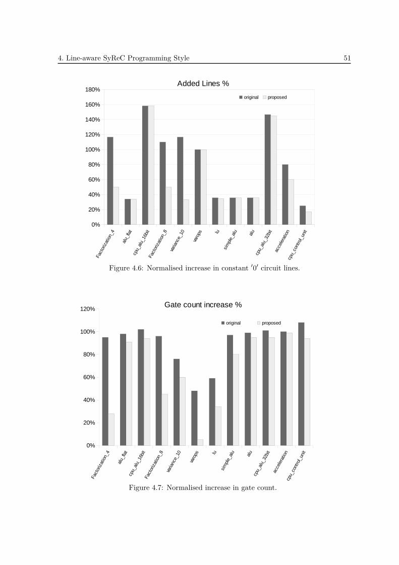
4. Line-aware SyReC Programming Style 51
Figure 4.6: Normalised increase in constant ′0′ circuit lines.
Figure 4.7: Normalised increase in gate count.

52 Experimental Evaluation
Figure 4.8: Normalised increase in quantum cost.
Figure 4.9: Normalised increase in transistor cost.

4. Line-aware SyReC Programming Style 53
4.3 Summary
In this chapter, we proposed a SyReC programming style oriented towards optimisedcircuit synthesis. The primary optimisation objective is to reduce the number of constantinputs for which SyReC with line-aware synthesis is considered. The secondary objective isto avoid, or at least to reduce, the cost-for-line trade-off associated with line-reduction. Thestyle is based on describing the desired function with as short expressions as possible guidedby the following:
1. Splitting assignment statements by replacing some non-reversible binary operators bytheir equivalent reversible assignment operators (Section 4.1.1).
2. Substituting the operands of large expressions by an internal wire identifier (Section 4.1.2).
3. Temporary signal update, with inverse-update when necessary (Section 4.1.3).
An experimental evaluation carried out to compare the spontaneous and the proposedSyReC programming styles with results showing a significant improvement, in one or bothoptimisation objectives, in the clear majority of these SyReC benchmarks (Section 4.2).
The proposed style shows code that is less readable, as compared to the spontaneouslywritten code. The modules are described with sorter expressions and with a large numberof statements. The most interesting observation in this experiment is that the reductionin the number of lines is not accompanied with extra cost. In fact, the partial increase iscompensated within the circuit, in all benchmarks.
Overall, the evaluation shows that re-writing the SyReC description for reversible circuitsynthesis is a promising direction to obtain compact results compared to the currentstate-of-the-art.
An interesting observation is that despite the theoretical possibility, none of thesebenchmarks shows a negative impact on any circuit parameter as a cost for line trade-off.These trade-offs where partial and are compensated within the circuit in all benchmarks.This observation shows that re-writing SyReC descriptions for reversible circuit synthesis isa promising direction to obtain more efficient tool for HDL-based synthesis.


55
Chapter 5
Optimised Synthesis of SyReCExpressions
The line-aware SyReC programming style proposed in Chapter 4 tackles the problemof constant inputs within the source code before working with the synthesis phase. Thisarrangement results in better circuits, but it compromises spontaneous HDL programmingand the code readability. Even with a fully automated code conversion, human interventionwill be expected for further tasks, such as debugging, which will be more complicated withless readable code. This contradicts a basic HDL characteristic, which is the simplicityof description, especially when handling complex problems. In this chapter, we analysethe problem at another level of abstraction, which is transparent to the programmer, toachieve line-awareness even with a spontaneous programming style. As we have alreadyidentified, SyReC expressions are the main source of constant inputs in the circuit. Hence,if line-awareness, as an objective, is considered when realising expressions, it may solve theproblem, at least to some extent, without the need to change the style of programming inSyReC.
It is important not to be confused with the line-aware statement synthesis configurationintroduced in Section 3.3, where expressions are computed in the same way and thenre-computed to free the garbage lines. Here, we propose a procedure to compute SyReCexpressions with line-awareness (i.e., with fewer lines).
In the first section of this chapter, computation of SyReC expressions are reviewed withmore details as compared to the brief review in Section 3.2.2. The modified line-awaresynthesis algorithm is proposed in Section 5.2. Circuit cost is considered in Section 5.3along with other related issues discussed before the experimental evaluation is introduced inSection 5.5.

56 SyReC Expressions
5.1 SyReC Expressions
An expression, as defined in SyReC grammar, can be a numeral, a signal identifier oran operation on some operand(s). The latter is a combined structure of an operator alongwith its operand(s) has to be computed (see Table 3.3). Operands, in the general case, arealso defined to be an expression. This recursive definition allows one expression to describecomplex computations. SyReC defines a reversible circuit to compute each operation, sooperations are considered basic building blocks (the lowest level in the synthesis hierarchy).These circuits were introduced in detail in [63]. In this chapter, a single operation isconsidered a unit of computation, i.e., the complexity of an expression is measured asthe number of operations performed to compute it. Table 3.3 shows two types of SyReCoperators:
1. Binary operators � with two operands EL and ER. A binary expression is defined withmandatory parentheses, i.e., (EL � ER).
2. Unary operators with only one operand EU directly to the right of the operator, i.e.,EU . There are only two such operators in SyReC (˜ and !).
An expression can be computed only when its operand(s) are already computed. Thisgives a tree structure to the expression where a node represents an operation, and an edge isa reference to an operand. The symbol of an operation is written inside the node. Figure 5.1provides symbolic representations of these nodes where
(a) a node of a binary operation has two edges, one black edge and another grey edge,referring to its left and right operands, respectively.
(b) a node of a unary operation has only one black edge referring to its operand.
EL ER
�(EL � ER)
(a) Binary
EU
EU
(b) Unary
Figure 5.1: Tree representation of SyReC operations.
Example 22. The SyReC expression (((a * b) / ˜(c + a)) - ˜(b * c)) iscomputed using seven operations, and Figure 5.2 shows the tree representation of thisexpression. The top-level operation in the expression (subtraction (-)) is the root nodeof the tree. Subtraction is a binary operation with two operands, and both are expressions.The left operand is ((a * b) / ˜(c + a)) and the right operand is ˜(b * c), each ofwhich is a sub-tree in the structure. The expression should be parsed and recursively computedusing the same steps for each sub-tree until reaching the primary signals at the tree bottom.

5. Optimised Synthesis of SyReC Expressions 57
− −
−7
∼6
b c
∗5− −
÷4
∼3
c a
+2a b
∗1
(((a ∗ b)/ ˜(c+ a))−˜(b ∗ c))
Figure 5.2: Expression tree for Example 22.
As shown in Figure 5.2, the precedence of an operation (the order of computation) istagged to the left of the node as an integer, i.e., the node tagged 1 is computed first, so thetop-level node is tagged with the highest number, i.e., 7 in this expression. The tree-bottomshows primary values, such as signal identifiers or numbers, which require no computation.In other words, each operator has lower precedence as compared to those operators used incomputing its operand expression(s).
5.1.1 Circuit Realisation of SyReC Operations
SyReC is not restricted to reversible operations, as shown in Table 3.3. The majority ofoperations defined by SyReC are irreversible. Consequently, a constant input is applied tothe circuit to compute the operation.
0 (EL � ER)
EL EL
ER ER
�
(a) Binary Operation
0 EU
EU EU
(b) Unary Operation
Figure 5.3: Schematic representation of SyReC operations.
Figure 5.3 shows the symbolic representation of a SyReC operation in a schematicdiagram, such that:
(a) A circuit of a binary operation G� is computed to a target line with constant ′0′
input. The two operands are connected from two inputs serving as control lines inthe reversible circuit. The left operand EL is identified by a black dot, while a greydot identify the right operand ER. At the output side of the circuit the expression,(EL�ER) is computed to the target line while the two operands’ lines are unchanged.

58 SyReC Expressions
(b) A circuit of a unary operation G is also computed to a line with constant ′0′ input.Here, only one input is serving as a control line in the reversible circuit. A black dotidentifies the operand EU . At the output side of the circuit, the expression EU iscomputed to the target line while the operand line is unchanged.
This schematic representation keeps the discussion at a high-level of abstraction byhiding the gate-level details, such as the bit-widths influence on the circuit details. Thelevel of discussion is comparable to register-transfer level in the design flow of conventionalcircuits, e.g., Figure 5.4 shows a 2-bit addition expression (a + b). The circuit on thegate level in Figure 5.4(a) shows more details as compared to the schematic representationin Figure 5.4(b). In this chapter, circuit realisation and synthesis is maintained at this levelwithout being involved in the circuit details, especially those related with the bit-width.Consequently, each operation is considered a unit building block in the expression circuit,and its bit-width is considered a single line for the remainder of this chapter.
a.0 a.0a.1 a.1b.0 b.0b.1 b.1
0 o/p.00 o/p.1
(a) Gate-level
0 (a+ b)
b b
a a
+
(b) Schematic
Figure 5.4: SyReC defined 2-bit addition G(a+b).
5.1.2 SyReC Synthesis of Combined Expressions
The discussion in Section 5.1.1 assumes the operands are already available, and ignoresthe fact that these operands require computation if they are expressions. SyReC doesnot provide a ready circuit definition for combined expressions (those with more than oneoperation), but synthesise such expression as a sequence of cascading operation blocks.
For a combined binary expression (EL�ER), the circuit G(EL�ER) is realised by cascadingthree parts as described in Equation 5.1:
G(EL�ER) = GEL GER G� (5.1)
where GEL and GER are the circuits to compute the left and right operands EL and ER,respectively, and G� is the defined circuit to compute the top-level binary operation �.On the other hand, only two parts are required to synthesise the circuit GEU of a unaryexpression, EU . First, the operand EU is computed using the circuit GEU , then it iscascaded by the operation circuit G, as described in Equation 5.2:
GEU = GEU G (5.2)

5. Optimised Synthesis of SyReC Expressions 59
1 2 3 4 5 6 7
01
02
03
04
05
06
07
a a
b b
c c
−
−
−
−
−
−
E
ER
EL
GELGER
G�
∗
+
∼
÷
∗
∼
−
Figure 5.5: Block diagram for SyReC synthesis of the expression in Example 22.
This recursive synthesis of operand computation continues until reaching a signal identifieror a number, which does not need any computation. In other words no circuit is needed tocompute this operand. This is the base case for the recursion.
In practice, SyReC parses the expressions into tree structures and traverses these trees toidentify the precedence of operations to determine the order by which circuits are cascaded.
Example 23. The expression (((a * b) / ˜(c + a)) - ˜(b * c)) in Example 22is computed as shown in Figure5.5. The circuit cascade follows the operation precedence asspecified in Figure 5.2, which begins by computing the operation tagged with number 1, i.e.,(a * b), and so on until the top top-level subtraction operation - is computed at the finalstage of the cascade.
5.1.3 Constant Inputs
A constant ′0′ line is applied to the input of the circuit for each operation used to computethe expression in Figure 5.5. This yields a circuit GE that computes an expression E realizedwith k constant ′0′ lines applied to its input when E is computed using k operations, as willbe explained in next. Figure 5.6 shows the schematic symbol for a generic expression circuit,GE .
In more detail, Figure 5.7 shows the generic schematic diagram to realise (a) a binaryexpression, G(EL�ER), and (b) a unary expression, GEU , which both show how constant ′0′
lines are accumulated to be (λE = k) as follows:
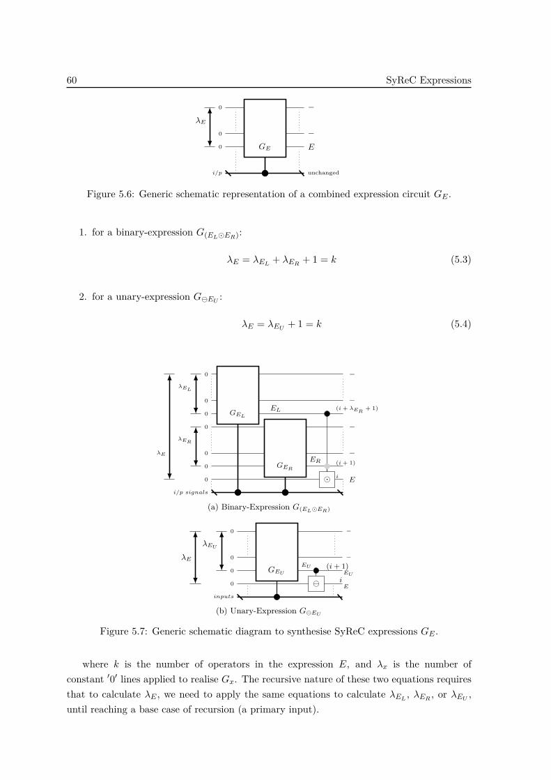
60 SyReC Expressions
GE
i/p
0
0
0
E
−
−
unchanged
λE
Figure 5.6: Generic schematic representation of a combined expression circuit GE .
1. for a binary-expression G(EL�ER):
λE = λEL + λER + 1 = k (5.3)
2. for a unary-expression GEU :
λE = λEU + 1 = k (5.4)
�GER
GEL
i/p signals
0
0
0
0
0
0
0
E
−
EL
ER
−
−
−
i
(i + 1)
(i + λER+ 1)
λER
λEL
λE
(a) Binary-Expression G(EL�ER)
GEU
inputs
0
0
0
0
E
EU
−EU
−
i
(i+ 1)
λEU
λE
(b) Unary-Expression GEU
Figure 5.7: Generic schematic diagram to synthesise SyReC expressions GE .
where k is the number of operators in the expression E, and λx is the number ofconstant ′0′ lines applied to realise Gx. The recursive nature of these two equations requiresthat to calculate λE , we need to apply the same equations to calculate λEL , λER , or λEU ,until reaching a base case of recursion (a primary input).
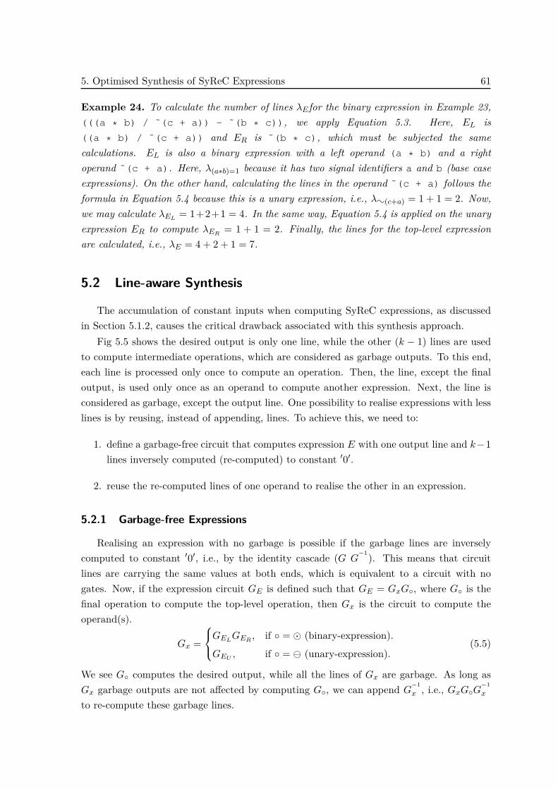
5. Optimised Synthesis of SyReC Expressions 61
Example 24. To calculate the number of lines λEfor the binary expression in Example 23,(((a * b) / ˜(c + a)) - ˜(b * c)), we apply Equation 5.3. Here, EL is((a * b) / ˜(c + a)) and ER is ˜(b * c), which must be subjected the samecalculations. EL is also a binary expression with a left operand (a * b) and a rightoperand ˜(c + a). Here, λ(a∗b)=1 because it has two signal identifiers a and b (base caseexpressions). On the other hand, calculating the lines in the operand ˜(c + a) follows theformula in Equation 5.4 because this is a unary expression, i.e., λ:(c+a) = 1 + 1 = 2. Now,we may calculate λEL = 1+2+1 = 4. In the same way, Equation 5.4 is applied on the unaryexpression ER to compute λER = 1 + 1 = 2. Finally, the lines for the top-level expressionare calculated, i.e., λE = 4 + 2 + 1 = 7.
5.2 Line-aware Synthesis
The accumulation of constant inputs when computing SyReC expressions, as discussedin Section 5.1.2, causes the critical drawback associated with this synthesis approach.
Fig 5.5 shows the desired output is only one line, while the other (k − 1) lines are usedto compute intermediate operations, which are considered as garbage outputs. To this end,each line is processed only once to compute an operation. Then, the line, except the finaloutput, is used only once as an operand to compute another expression. Next, the line isconsidered as garbage, except the output line. One possibility to realise expressions with lesslines is by reusing, instead of appending, lines. To achieve this, we need to:
1. define a garbage-free circuit that computes expression E with one output line and k−1lines inversely computed (re-computed) to constant ′0′.
2. reuse the re-computed lines of one operand to realise the other in an expression.
5.2.1 Garbage-free Expressions
Realising an expression with no garbage is possible if the garbage lines are inverselycomputed to constant ′0′, i.e., by the identity cascade (G G
−1). This means that circuitlines are carrying the same values at both ends, which is equivalent to a circuit with nogates. Now, if the expression circuit GE is defined such that GE = GxG◦, where G◦ is thefinal operation to compute the top-level operation, then Gx is the circuit to compute theoperand(s).
Gx =
GELGER , if ◦ = � (binary-expression).
GEU , if ◦ = (unary-expression).(5.5)
We see G◦ computes the desired output, while all the lines of Gx are garbage. As long asGx garbage outputs are not affected by computing G◦, we can append G
−1x , i.e., GxG◦G
−1x
to re-compute these garbage lines.

62 Line-aware Synthesis
1 2
c c
b b
a a
0
0 +
∗ E
−(b + c)
GE
(a) GE with a garbage line
1 2 3
c c
b b
a a
0
0 +
∗
+−1
EE
0−(b + c)
GE
(b) G′E with no garbage
Figure 5.8: Two equivalent realisations for G(a∗(b+c) in Example 25.
Example 25. (a*(b+c)) is an expression (E) composed using two operations. Figure 5.8ashows the circuit diagram of GE with a garbage line at the output end. The circuit issynthesised by cascading two operations and required two constant ′0′ lines. In this expression,Gx = G+ is the first operation, and the second is G∗, which calculates the final output.GE = G+ G∗ has to be cascaded by G−1
x = G−1+ to re-compute the garbage line, as shown in
Figure 5.8b, which is the garbage-free circuit, G′E = G+ G∗ G−1+ .
G′E,i
i/p
0
0
0
iE
0
0
unchanged
λE
Figure 5.9: Generic representation of a garbage-free Circuit G′E .
To generalize; we define G′E to be the garbage-free equivalent of GE , where all
intermediate lines are re-computed to constant ′0′ (Figure 5.9) as:
G′E = Gx G◦ G
−1x = GE G
−1x (5.6)
This circuit cascade is schematically represented in Figure 5.10.
By substituting Gx as defined in Equations 5.5 and 5.6, we obtain the following twoequations:
G′
(EL�ER) = GEL GER G� G−1ER
G−1EL
(5.7)
G′EU = GEU G G
−1EU
(5.8)

5. Optimised Synthesis of SyReC Expressions 63
unchangedi/p
◦
Gx G−1x
i
GE
G′
E
0
0
0
0
E
0
0−
−
−0
Figure 5.10: A schematic diagram for the garbage-free realisation G′E .
With this approach, we defined garbage-free circuits that realise SyReC expressions witha higher cost, due to the extra circuitry of inverse computation Gx, but with no impact onthe number of lines used. Here, we have no advantage unless this arrangement is invested inreusing lines.
5.2.2 Reusing Constant Inputs
After re-computing, lines are eligible to be used in another computation. For example, ina binary expression, (EL � ER), when the left-operand EL is computed with a garbage-freecircuit G′EL , then the re-computed lines can be used in computing the right operand, GER .This modifies the circuit definition in Equation 5.1 to be
G(EL�ER) = G′EL
GER G�. (5.9)
We can see the number of constant lines applied depends on the largest operand (seeFigure 5.11(a)), i.e., λE = max〈(λEL + 1), (λER + 2)〉 instead of the summation, i.e.,
λ(EL�ER) =
λEL + 1, if λEL > λER
λER + 2, if λEL 6 λER
(5.10)
Consequently, the definition of the garbage-free equivalent of this circuit G′E , as definedby Equation 5.7, should also be modified to incorporate this scheme (see Equation 5.11).The number of lines applied to realise G
′E is the same number of lines computed from
Equation 5.10 (see Figure 5.11(b)).
G′
(EL�ER) = G′EL
GER G� G−1ER
G′−1EL
(5.11)
Line-ware synthesis of SyReC expressions follows the circuit cascades as described inEquations 5.9 and 5.11, as well as 5.2 and 5.8, which are mutually recursive.

64 Line-aware Synthesis
inputs
0
0
0
0
0
E
EL
ER
EL
ER
−
−
0
0
i
i+ 1
i+ 2
λER+ i+ 1
λEL+ i
�
GER
G′EL
λER
λEL
λE
(a) G(EL�ER)
inputs
0
0
0
0
0
E
0
0EL
ER
0
0
0
0
i
i+ 1
i+ 2i+ 2
�
GER
G′EL
G−1ER
G′−1EL
λER
λEL
λE
(b) G′
(EL�ER)
Figure 5.11: Schematic diagram for garbage-free line-aware binary expression synthesis.
Example 26. Applying Equations 5.9 and 5.11 instead of Equations 5.1 and 5.7 to realisethe expression in Example 22 results in a circuit with 5 constant ′0′ lines (Figure 5.12), ascompared to 7 in Figure 5.5. Here, G′EL is computed instead of GEL, with lines’ numbers3, 4, and 5 being re-computed (shaded area). Then, lines 3 and 4 are reused in computingGER instead of lines 6 and 7 in Figure 5.5. The total number of lines λE for this expressionis calculated from Equation 5.10, such that λE = (4 + 1) = 5.
5.2.3 Operands Order in Synthesis
Both original SyReC and line-aware synthesis of binary expressions as proposed inSections 5.1.2 and 5.2.2, respectively, start with computing the left operand circuit GELfirst before computing the right operand GER . This default case is not mandatory becausethe operands are independent of each other. The only consideration is to guarantee thatboth operands are computed before the top-level operation. There is no reason to changethe usual conventional computing of left to right as long as the order is irrelevant. To thisend, this assumption applied to the original SyReC synthesis, which calculates the lines λEfrom Equation 5.3 as a total sum of lines. On the other hand, the number of lines may differif λEL and λER are swapped within Equation5.10.
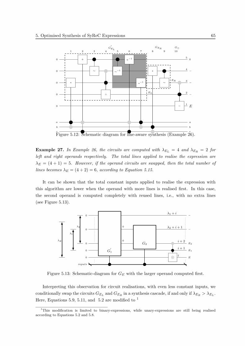
5. Optimised Synthesis of SyReC Expressions 65
1 2 3 4 5 6 7 8 9 10
01
02
03
04
05
a a
b b
c c
∗
+
∼
÷
∼−1
+−1
∗−1
∗
∼
−
−
0
−
−
E
ER
EL
G′EL
GERG�
Figure 5.12: Schematic diagram for line-aware synthesis (Example 26).
Example 27. In Example 26, the circuits are computed with λEL = 4 and λER = 2 forleft and right operands respectively. The total lines applied to realise the expression areλE = (4 + 1) = 5. However, if the operand circuits are swapped, then the total number oflines becomes λE = (4 + 2) = 6, according to Equation 5.15.
It can be shown that the total constant inputs applied to realise the expression withthis algorithm are lower when the operand with more lines is realised first. In this case,the second operand is computed completely with reused lines, i.e., with no extra lines(see Figure 5.13).
inputs
0
0
0
0
0
E
E1
E2
−
−
0
0
i
i+ 1
i+ 2
λ2 + i+ 1
λ1 + i
�
G2
G′1
λ2
λ1
λE
Figure 5.13: Schematic-diagram for GE with the larger operand computed first.
Interpreting this observation for circuit realisations, with even less constant inputs, weconditionally swap the circuits GEL and GER in a synthesis cascade, if and only if λER > λEL .Here, Equations 5.9, 5.11, and 5.2 are modified to 1
1This modification is limited to binary-expressions, while unary-expressions are still being realisedaccording to Equations 5.2 and 5.8.

66 Line-aware Synthesis
( G1 , G2 , λ1 , λ2) =
( GEL , GER , λEL , λER) if λEL > λER
( GER , GEL , λER , λEL) if λEL < λER
(5.12)
G(EL�ER) = G′1 G2 G� (5.13)
G′
(EL�ER) = G′1 G2 G� G−1
2 G′−11 (5.14)
λ(EL�ER) =
λ1 + 1, if λ1 6= λ2
λ1 + 2, if λ1 = λ2(5.15)
Example 28. Applying Equations 5.13, 5.14, 5.2, and 5.8 to realise the expression inExample 26 realises the circuit with only 4 constant lines applied to its inputs,i.e., with one line less because of operands’ reorder (see Figure 5.14). Here, the left operandEL =((a * b) / ˜(c + a)) is an expression with a left operand ELL =(a * b) andELR =˜(c + a) with (λELL = 1) 6= (λELR = 2). Now, applying Equation 5.15 to determinethe number of lines gives λE = 2 + 1 = 3 lines applied to compute G
′EL
(lines 2, 3, and4) as shown in Figure 5.14. The right operand of the top-level operation ER requires twoconstant lines to be realised λER , i.e., completely computed using re-computed lines and nonew line is required. The total number of applied constant inputs to compute the expressionis λE = λ1 + 1 = (3 + 1) = 4 as shown in Figure 5.14.
1 2 3 4 5 6 7 8 9 10 11 12
01
02
03
04
a a
b b
c c
÷
∼
÷−1 ∗
+
∗−1 ÷
∼−1
÷−1 ∗
∼
−
0
−
−
E
ER
EL
G′EL
GERG�
Figure 5.14: Line-aware synthesis with operands’ reorder (Example 28).
It might be considered an insignificant reduction of only one line, but it provides a20% improvement in this example (1/5 lines). The recursive nature of this procedure givesoperand reorder the possibility to reduce a line for each stage in the recursion. This mayresult in many lines reduced from the overall realisation of the circuit depending on the shapeof the expression tree.

5. Optimised Synthesis of SyReC Expressions 67
5.2.4 Reversible Operators
SyReC realises expression operations with the assumption that they are irreversible(see Section3.2.2), which allows the synthesis of any operation by applying a constant ′0′
line (see Figure 5.3). This assumption ignores some operations that are reversible, such as(+,-,ˆ,˜,!), which are not many, but intensively used. This exceptional reversibilityallows updating the operand instead of applying a constant input to compute the operation(see Figure 5.15).
On the gate level, this reversible realisation is similar, to replacing irreversible binaryoperators with their equivalent reversible assignments in the source code, e.g., replacing +
with +=. Hence, we will use ⊕ = and = in the remainder of this chapter for binary andunary operations, respectively, whenever they are reversibly realised.
EU EU =
(a) GEU
ER (EL ⊕ ER)
EL EL
⊕ =
(b) G(EL⊕ER)
EL (EL ⊕ ER)
ER ER
⊕ =
(c) G(EL⊕ER)
Figure 5.15: Schematic representation of reversible operators.
The updated operands in Figure 5.15 are underlined. Figures 5.15(b) and 5.15(c)are computing the same expression with the only difference being the updated operand.The updated operands should never be a signal identifier because this would violate theassumption of unchanging inputs while computing the expression. In other words, this cannotbe applied if both operands are signal identifiers, e.g., (a + b), where both a and b aresignal identifiers. This reversible computation changes the entire realisation, consequently,as all equations describing the circuit are changed. This modification can realise expressionswith fewer lines as well as with less cost.
5.2.4.1 Unary Expressions
All unary expressions are reversible because the operations ˜ and ! are reversible. Areversible computation updates the line to which the operand is computed, as follows:
GEU = GEU G(=) (5.16)
G′EU = G
′EU
G(=) (5.17)
Equations 5.16 and 5.17 differ in that realising the operand with a garbage-free circuit, G′EU ,results in a garbage-free realisation G′EU , and vice versa (see Figure 5.16). This means thatthe number of lines applied to compute the expression is used for the operand, i.e., one lineless in Equation 5.18 than in Equation 5.4.
λEU = λEU (5.18)

68 Line-aware Synthesis
inputs
0
0
0
EU
EU
0
00
0
i
i + 1
=GEU
λEU
(a) GEU
inputs
0
0
0
EU
EU
0
00
0
i
i + 1
=G′EU
λEU
(b) G′EU
Figure 5.16: Schematic diagram for unary expressions using G(=).
5.2.4.2 Binary Expressions
Reversible computation of ⊕, i.e., G⊕= updates the same line by which G1 is computed,and, hence, this operand should not be re-computed at the end of the cascade of garbage-freecircuits, (see Figure 5.17). Such circuits compute G′(EL⊕ER) with one line less and with evenless cost, as compared to Section 5.2.3. These circuits are described by Equations 5.19, 5.20,and 5.21 instead of Equations 5.13, 5.14, and 5.15 in Section 5.2.3.
inputs
0
0
0
E
E2
E1
−
−0
0
i
i + 1
⊕ =
G2
G′1
λ2
λ1λE
(a) G(EL ⊕ ER)
inputs
0
0
0
E
E2
E1
0
00
0
i
i + 1
⊕ =
G2
G′1
G−12
λ2
λ1λE
(b) G′
(EL ⊕ ER)
Figure 5.17: Schematic diagram for binary expressions using G(⊕=).
G(EL⊕ER) = G′1 G2 G(⊕=) (5.19)
G′
(EL⊕ER) = G′1 G2 G(⊕=) G−1
2 (5.20)
λ(EL⊕ER) =
λ1, if λ1 6= λ2
λ1 + 1, if λ1 = λ2(5.21)

5. Optimised Synthesis of SyReC Expressions 69
Example 29. Figure 5.18 shows the same expression as in Example 28, where only threeconstant input lines are applied to the circuit. The circuit is computed with ten operationsas compared to twelve in Example 28.
1 2 3 4 5 6 7 8 9 10
0
0
0
01
02
03
a a
b b
c c
+ ∼=
∗
÷
+−1∼=−1
∗−1 ∗ ∼=
− =
00
−
E
ER
EL
G′EL
GERG⊕
Figure 5.18: Computing the expression in Example 29.
Examples 25, 26, and 28 compute the same expression using three different, yet equivalent,realisations, which demonstrate the cost-for-lines trade-off as the circuit with fewer linesis realised with higher cost (more operations) as presented by the curve in Figure 5.20.This figure shows that Example 29 is an exception as it falls below the trade-off curvemeaning that, in a reversible paradigm, reversible computations are easier than non-reversiblecomputations.
5.3 Cost-aware Synthesis
In the reversible paradigm, circuit synthesis approaches have the two optimisation trade-offobjectives of the desired function with as few circuit lines and with as low gate cost aspossible. Section 5.2 introduced circuit lines as the main objective for optimization, andpromotes line-aware realisations. These realisations are trading reduced lines with extracost, except in Section 5.2.4, where a reduction in lines is not traded in with extra cost.
Cost is the other important circuit metric. First, we discuss the impact of line-awarerealisations on circuit cost followed by an investigation of possible modifications to avoidor reduce cost trade-offs without compromising the reduced number of lines obtained inSection 5.2.

70 Cost-aware Synthesis
5.3.1 Cost-line Trade-offs
Figures 5.5, 5.12, and 5.14 show three different realisations to compute the sameexpression E in Example 22. The lines and cost parameters of each realisation is shown inFigure 5.20 in which we can see a trade-off curve for these realisations. The cost metric usedin this graph is the overall number of operations β used to compute the expression 2, includinginverse-computations (re-computation). Since all realisations are similar in the number ofoperations (for the same expression), the difference in the total number of computationsarises from the inverse-operations. Here, we know for certain that in a garbage-free circuit,βG′E> βGE . In this case realising the operand with the lower cost first results in less overall
circuit cost. Consequently, Equation 5.12 is modified such that the operands are rearrangedto compute the one with lower cost first when both are realised with the same number ofconstant inputs:
(G1, G2, λ1, λ2) =
(GEL , GER , λEL , λER) if λEL > λER
(GER , GEL , λER , λEL) if λEL < λER
(GER , GEL , λER , λEL) if (λEL = λER)AND(βL > βR)
(5.22)
5.3.2 Partial (incomplete) Re-compute
Line-aware realisation of expressions, as proposed in Section 5.2, re-computes garbagelines applied to compute an operand for reusing these lines in computing the other operandin a binary expression. So all garbage lines are re-computed. The algorithm rearrangesthe order of computing the operands such that the operand G1 is realised before G2 whenλ1 > λ2 (see Section 5.2.3). If (λ1 − λ2) 6 1, then all re-computed lines are reused torealise G2, but when (λ1−λ2) > 1, there exist re-computed line(s) that are not reused, e.g.,in Figure 5.18 where line 3 is re-computed but not reused. In this case, inverse operationsadd cost for no reason. This superfluous cost can be identified and reduced, by removingthese inverse-operations from the circuit, as follows:
1. If the expression is binary (EL�ER), and (λ1−λ2) < 1 6 l, then the circuit incorporates(l − 1) lines that do not have to be re-computed.
2. To identify an operation that is unnecessarily re-computing a line:
(a) The operation is a part of a re-compute circuit G−1x of the first operand G
′1 (the
space with grey background).
(b) The line to which this operation is computed is not used after this operation,neither as a control nor as a target line.
2Operation count is used as a cost indicator assuming each operation has the same unity cost metric. Thisassumption is very far from being accurate as there are considerable differences in the complexity of operators’circuits. This assumption provides a reasonable operator-independent assessment to algorithms efficiency inthis context.

5. Optimised Synthesis of SyReC Expressions 71
3. To remove these inverse operations, start from the last operation within G−1x :
(a) Check if it is removable,
(b) if yes, remove and go to the operation before, and
(c) repeat until the first operation in the re-compute circuit is checked.
Example 30. In Figure 5.18, the left operand G′EL is realised by applying λL = 3 constant,and the right-operand GER is realised by applying λR = 1, (λL − λR) = 2, i.e., there exists(2 − 1 = 1) unnecessarily re-computed line (line 3). The shaded area in this figure showsthe inverse computation of garbage lines of the left operand, i.e., operations (5, 6, and 7).Figure 5.19 is identical to Figure 5.18. Starting from 7 back to 5, the operation is checked.Here, operations 6 and 5 are both re-computing line 3, which is not used in the rest of thecircuit, so both operations are removed.
This incomplete operand re-compute modifies the proposed realisation to improve circuitcost without compromising the minimum line achieved by line-aware realisation, as proposedin Section 5.2 (see Figure 5.20).
1 2 3 4 5 6 7 8 9 10
0
0
0
01
02
03
a a
b b
c c
+ ∼=
∗
÷
+−1∼=−1
∗−1 ∗ ∼=
− =
−−
−
E
ER
EL
G′EL
GERG⊕
Figure 5.19: Block diagram of the expression in Example 22 with garbage partiallyre-computed.
5.4 Manipulating Expressions
Sections 5.2 and 5.3 propose different ways to compute a SyReC expression and showthe impact of each algorithm on the number of lines and costs of the resulting circuits. Oneobservation is that the order of computing the operations does matter (see Section 5.2.3).This motivates investigating the impact of the expression-tree shape on the resulting circuits.
In this section, we discuss further improvements on circuits by manipulating the orderof operations in computing expressions by considering properties of operations, such as theassociative and commutative properties.

72 Manipulating Expressions
Lines
Operations
7
10
12
8
3 4 5 7
?Figure 5.18
• Figure 5.14
• Figure 5.12
• Figure 5.5
? Figure5.19
Figure 5.20: Lines vs. cost metrics of circuits in Figures5.5, 5.12, 5.14, 5.18, and 5.19.
Example 31. Figure 5.21 shows trees of three different expressions, which compute theproduct of eight signals. The expressions are mathematically equivalent to each other becausemultiplication (*) is associative:
1. Figure 5.21(a) shows E1 = (((((((a*b)*c)*d)*e)*f)*g)*h) in which eachoperation has one operand as a primary signal.
2. Figure 5.21(b) shows E2 = (((a*b)*(c*d))*((e*f)*(g*h))) in which eachoperation has two operands with the same size(balanced tree).
3. Figure 5.21(c) shows E3 = ((((a*b)*c)*(d*e))*((f*g)*h)) in which eachoperation has the right operand realised using exactly one line less than the left operand.
Despite being equivalent, these expressions are realised with different circuits (see Figure 5.22):
1. Figure 5.22(a) shows E1 computed using 7 lines and 7 operations. The realisationis considered as the worst case in terms of constant inputs, where no operation isre-computed.
2. Figure 5.22(b) shows E2 computed using 5 lines and 9 operations. This balancedstructure shows a moderate reduction in lines and trade-off with some increase in cost.
3. Figure 5.22(b) showsE3 computed using 4 lines and 12 operations, which is consideredas the best case with respect to the number of lines and with extra cost.
Replacing multiplication (*) with addition (+) results in other expressions (E′1, E′2, and E′3),which compute the summation of the signals rather than the product. These expressionshave similar tree structures to their counterparts (i.e., E1, E2, and E3 respectively), yet thecomputations are obviously different. The fact that (+) can be replaced by the reversible (+=)changes the realisations, as shown in Figure 5.23.

5. Optimised Synthesis of SyReC Expressions 73
a b c d e f g h
∗
∗
∗
∗
∗
∗
∗
(a) E1 = (((((((a ∗ b) ∗ c) ∗ d) ∗ e) ∗ f) ∗ g) ∗ h)
a b c d e f g h
∗
∗
∗∗
∗
∗∗
(b) E2 = (((a ∗ b) ∗ (c ∗ d)) ∗ ((e ∗ f) ∗ (g ∗ h)))
a b c d e f g h
∗
∗
∗
∗
∗
∗∗
(c) E3 = ((((a ∗ b) ∗ c) ∗ (d ∗ e)) ∗ ((f ∗ g) ∗ h))
Figure 5.21: Three different equivalent expressions.
1. Figure 5.23(a) shows E′1 = (((((((a+b)+c)+d)+e)+f)+g)+h) computed in thebest possible way with reversible operations, and only one constant input is exploitedin this realisation with the summation using 1 constant line and 7 operations. On theother hand, the expression E1, which has the same tree structure is considered the worstcase in terms of lines.
2. Figure 5.23(b) shows E′2 = (((a+b)+(c+d))+((e+f)+(g+h))) witha perfectly-balanced tree structure with the worst realisation, in terms of lines. Thesummation exploits 3 lines and 8 operations.
3. Figure 5.23(c) shows E′3 = ((((a+b)+c)+(d+e))+((f+g)+h)) computed using 2lines and 8 operations, while the same tree structure resulted in the best case to computethe product (i.e., in E3).

74 Manipulating Expressions
1 2 3 4 5 6 7
1
2
3
4
5
6
7
h h
g g
f f
e e
d d
c c
b b
a a
0
0
0
0
0
0
0 *
*
*
*
*
*
* E
(a) Worst case expression E1
1 2 3 4 5 6 7 8 9
1
2
3
4
5
h h
g g
f f
e e
d d
c c
b b
a a
0
0
0
0
0
∗
∗
∗
∗−1
∗−1
∗
∗
∗
∗ E
(b) Perfectly-balanced expression E2
1 2 3 4 5 6 7 8 9 10 11 12
1
2
3
4
h h
g g
f f
e e
d d
c c
b b
a a
0
0
0
0 ∗
∗
∗−1 ∗
∗
∗−1 ∗
∗−1
∗−1 ∗
∗
∗ E
(c) Best case expression E3
Figure 5.22: Computing the expressions of Figure 5.21.
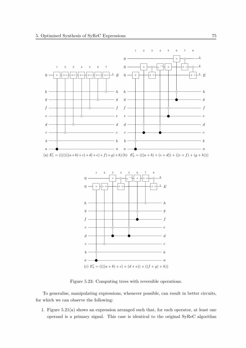
5. Optimised Synthesis of SyReC Expressions 75
1 2 3 4 5 6 7
1
h h
g g
f f
e e
d d
c c
b b
a a
0 + += += += += += += E
(a) E′1 = (((((((a+b)+c)+d)+e)+f)+g)+h)
1 2 3 4 5 6 7 8
1
2
3
h h
g g
f f
e e
d d
c c
b b
a a
0
0
0
+
+
+ =
+−1 +
+
+ =
+ = E
(b) E′2 = (((a+ b) + (c+ d)) + ((e+ f) + (g + h)))
1 2 3 4 5 6 7 8
1
2
h h
g g
f f
e e
d d
c c
b b
a a
0
0
+ + =
+
+ =
+−1 + + =
+ = E
(c) E′3 = ((((a+ b) + c) + (d+ e)) + ((f + g) + h))
Figure 5.23: Computing trees with reversible operations.
To generalise, manipulating expressions, whenever possible, can result in better circuits,for which we can observe the following:
1. Figure 5.21(a) shows an expression arranged such that, for each operator, at least oneoperand is a primary signal. This case is identical to the original SyReC algorithm

76 Manipulating Expressions
as no re-compute occurs. Here, (λ = k = n = b), where k is the number of operatorsin an expression, λ is the number of constant ′0′ circuit lines, b is the number ofoperations and n is the height of the binary tree. This is the worst case with respectto the number of lines, as the results show. However, when such a tree structure is tocompute reversible operations, such as (+=), the entire expression may be computedusing only 1 line, which is the best possible case.
2. Figure 5.21(b) shows a perfect binary tree, which exploits lines to be synthesized. Here,
λ = 2(dlog2(k + 1)e)− 1 = 2 · n− 1 (5.23)
where λ is logarithmically instead of linearly dependent on k. Practically, a perfectbinary tree is a special case that can occur only when the expression is composed using(k = 2n − 1) binary operators. Again, n is the height of the tree. The cost is expectedto increase exponentially as a trade-off where, in this case, the number of operations bis given by
b = 3(dlog2(k+1)e−1) = 3n−1 (5.24)
The same tree structure results in circuits that provide no advantage when theoperations are reversible (e.g., with +).
3. Figure 5.21(c) shows a best-case tree where the highest efficiency is obtained fromline-aware synthesis in terms of the number of lines. For all operations, the right-handoperand requires exactly one circuit line less than the left operand. Hence, rightoperands completely reuse lines and do not need to allocate another line. This caseshows the maximum usage of re-computed lines. Here, λ = n and the number ofoperators, k, in this case is recursively calculated using the sequence 3
k = κ(n) = κ(n− 1) + κ(n− 2) + 1 (5.25)
where κ(1) = 1 and κ(2) = 2. For example, if there are λ = 6 lines, then κ(6) = 20, i.e.,an expression arranged in the best case with up to k = 20 operations can be calculatedby using these lines. The total number of operations to compute the expressions isdetermined from the sequence
b = β(n) = 2 · β(n− 1) + β(n− 2) (5.26)
Manipulation is not always possible, but when it is, it would be better to have the maximumbenefit from the line-aware expression synthesis algorithms.
3This sequence is strongly related to the Fibonacci sequence f(n) = f(n − 1) + f(n − 1) whereκ(n) = f(n+ 2)− 1

5. Optimised Synthesis of SyReC Expressions 77
5.5 Experimental Evaluation
Expression realisations, as proposed in this chapter, are experimentally evaluated anddiscussed in this section. The aim is to assess the impact of the different ways to computean expression, in practice, on the resulting circuits.
The discussion in this chapter is carried out on a higher-level of abstraction, whichis comparable to the register-transfer level in conventional design flow, instead of at thegate-level. We deal with variable length unsigned integers as the data unit for which theoperations are defined. The usual gate-level metrics, as discussed in Section 2.2.5, becomeconfusing and not useful in evaluating the quality of the computations because they arerelated to gate-level details, such as operation bit-widths and the gate complexity of differentoperations’ circuits. Therefore, we suggest two metrics, which are coherent with the levelabstraction in this chapter:
1. Constant inputs (λ): The number of constant ′0′ lines applied to the circuit to computethe expression, Signal input lines are excluded from the count because they are notsubject to optimisation. Then, the number of lines are divided by the operator bit-widthin order to have a bit-width-independent line metric.
2. Operation blocks (β): The number of operations and inverse operations performed tocompute the expression. Each operation is identified as a unit circuit (a basic block)regardless of the actual gate cost of this specific operator circuit by which we can havean operation independent measure for the cost expansion.
The experiment carried out using a set of benchmark expressions with different sizes andstructures. Each expression is realised five times using the following configurations:
(R1) Direct synthesis as originally performed by SyReC synthesiser, as explained inSection 5.1.2.
(R2) A line-aware synthesis as proposed in Section 5.2.2.
(R3) A line-aware synthesis with rearranged operands, such that the first is computed first,as proposed in Section 5.2.3.
(R4) Scenario (R3) modified to incorporate reversible updates when computing specialoperations, i.e., ⊕ = and =, as proposed in Section 5.2.4.
(R5) Scenario (R4) with incomplete re-compute of garbage lines, as proposed in Section 5.3.2.
Table 5.1 shows λ and β measured for each realisation as well as the number of operatorsused to compute the benchmark k. From this table, we observe:
1. all configurations have the same results for small expressions (three or fewer operations).On the other hand, large expressions show significant differences between circuits inboth λ and β configurations. It is true that complex expressions are not the trend in

78 Experimental Evaluation
HDL programming, but such expressions may appear, e.g., as complex conditionals.Having just one such expression in the entire module is enough to set a lower boundto the constant inputs applied to the circuit.
2. (R5) is always better than (R3) and (R4) in both measures. Consequently, the onlythree alternatives proposed are (R2), (R5), and the original (R1). Therefore, thecomparison graphs in Figure 5.24 and Figure 5.25 include only the realisations R1, R2,and R5.
3. (R1) always has the lowest β. Consequently, there is no need to use another alternativeexcept for the largest expression in a module, i.e., the most line demanding expression,which sets a bound for the number of constant inputs in the entire circuit. Here, it isbetter to compute the expression with fewer lines.
4. (R5) always has the lowest λ. Therefore, it is the one to be used for the largestexpression in a module. On the other hand, configuration (R2) may have someadvantage over (R5) in cases when it computes with less β if λ is good enough.
5. The reduction of constant lines in configurations (R2) and (R3) depends on the numberof lines in the two operands’ sub-circuits. Maximum reduction is obtained when theright operand is realised using one line less than the left operand (λEL = λER + 1).
6. Scenario (R4) shows a reduction in both parameters without any trade-off only whenthe expression contains some reversible operators ( ! , ˜ , ˆ , - , +); otherwise,it has no impact on the circuit.
7. Scenario (R5) shows a tangible reduction in cost as compared to scenario (R3) whenthere is a large difference in the number of lines between the two operands’ sub-circuits(λEL � λER) or (λEL � λER).
8. From observations 5 and 7 above, we can better understand the influence of the shapeof an expression tree on the circuits, which was discussed in Section 5.4. Taking thisinto consideration, programmers may improve writing their expressions such that:
(a) binary expressions with the form ((E1 ⊕ E2)⊕ S) instead of (E1 ⊕ (E2 ⊕ S)),where E1, E2 are two expressions and S is a primary signal. This suggestionmaps to better circuit costs and fewer lines in some cases.
(b) expressions arranged in the worst case are avoided. It is much better to have anexpression written as (E1 � (E2 � S)) instead of ((E1 � E2)� S), where E1 is alarge expression, E2 is smaller and S is a primary signal. It is better, wheneverpossible, to split the expression such that one operand is slightly smaller than theother. More precisely, it is better to have a smaller operand sub-expression withonly one line less than the larger operand sub-expression.

79
Tabl
e5.
1:Ex
perim
enta
leva
luat
ion
for
diffe
rent
benc
hmar
kex
pres
sions
’circ
uits
.
Ben
chm
ark
(R1)
Sect
ion
5.1.
2(R
2)Se
ctio
n5.
2.2
(R3)
Sect
ion
5.2.
3(R
4)Se
ctio
n5.
2.4
(R5)
Sect
ion
5.3.
2N
ame
kλ
βλ
βλ
βλ
βλ
β
ov4
11
11
11
11
11
1ac
c2
22
22
22
22
22
avsp
33
33
33
33
33
3p2
o4
44
35
35
35
35
maj
35
55
47
47
47
46
p3o
55
54
64
62
62
6f3
o6
66
57
48
48
48
exp7
77
75
105
103
83
8ex
mp7
77
75
104
123
103
18f4
o8
88
615
517
517
515
exp9
99
97
176
216
216
16av
1010
1010
714
618
412
412
exp1
111
1111
717
623
623
618
f8o
1616
169
129
814
58
145
866
se7
1717
178
307
424
284
27m
aj5
2929
299
114
914
49
114
911
1p8
o44
4444
1013
59
167
694
692
(k)
isth
enu
mbe
rof
oper
atio
nsin
the
benc
hmar
kex
pres
sion.
(λ)
isth
enu
mbe
rof
cons
tant
lines
expl
oite
dto
com
pute
the
expr
essio
n.(β
)is
the
tota
lnum
ber
ofop
erat
ions
and
inve
rse-
oper
atio
ns(r
e-co
mpu
te)
bloc
ksus
edto
com
pute
the
expr
essio
n.

80 Experimental Evaluation
Figure 5.24: Constant lines exploited to compute expressions in different realisations.
Figure 5.25: Costs of computing expressions in different realisations.
5. Optimised Synthesis of SyReC Expressions 81
5.6 Summary
In this chapter, various procedures are proposed to realise SyReC expressions. The mainobjective is to compute expressions with as few constant inputs as possible, without the needto change the programming style or compromise simplicity of HDL descriptions.
The secondary optimisation objective is to avoid the expected cost-for-line trade-off, ifpossible. This line-awareness is based on reusing lines to avoid applying new ones. Theexperimental results show that in many cases the proposed algorithms succeeded in reducingthe number of lines with relatively small increases in circuit cost.
Different realisations are discussed, with three proposed as candidates for use asalternatives to compute expressions. The basic realisation as originally defined in SyReC(i.e., without operation re-compute) is discussed in Section 5.1.2, and this realisation showsthe minimal cost. Hence, this approach is recommended when the circuit already provides asufficient number of constant inputs.
The realisation proposed in Section 5.3.2 is the one to compute expressions with fewerlines in most cases. Consequently, it is recommended when circuit lines are limited (e.g., whencomputing the largest expression in the module). In a few cases, the realization proposedin Section 5.2.2 shows better results as compared to Section 5.3.2. Therefore, this approachmay also be considered as an alternative.
Realising reversible circuits that compute HDL-expressions as proposed in this chapteris not exclusively applicable for SyReC. In fact, SyReC considers irreversible operationsin its expressions. Hence, the same approaches may be used to compute conventionalHDL-expressions if we can define reversible circuits for the operations of that HDL.

83
Chapter 6
Synthesis of Reversible Circuits UsingConventional HDL
An elaborated flow emerged over the last few decades for the design of circuits and systemsbased on the conventional computation paradigm. This flow is composed of several levelsof abstraction (e.g., specification level, electronic system level, register transfer level, gatelevel, and transistor level). A wide range of design tools has been developed and acceptedas standards in the industry, such as modelling languages, system description languages,and hardware description languages [18]. Furthermore, these design methodologies areadditionally supported by various powerful approaches for simulation, verification, validation,and debugging to ensure the correctness of a designed circuit or system. On the other hand,considering the reversible computation paradigm, none such powerful approach is availableso far. Although researchers have considered the basic tasks of synthesis, verification, anddebugging, reversible computation design flow is still elementary.
Many efforts have been made to investigate the suitability of conventional computationmethodologies for circuit design in the reversible computational paradigm at the gate leveldescription, such as Boolean expressions, truth tables, and binary decision diagrams [3,4,52].However, limited efforts are tackling the problem of reversible circuit design at a higherabstraction level. In comparison to matured conventional HDLs, SyReC is a preliminarylanguage with one data type and a basic set of operations. In other words, the existing designmethods for reversible circuits and systems are far from modern standards and industrialneeds. Consequently, investigating conventional HDL approaches for the design of reversiblecircuits may be advantageous over dedicated reversible HDL. However, very little exists inthe literature referring to conventional HDLs as a basis for reversible circuit design [63].
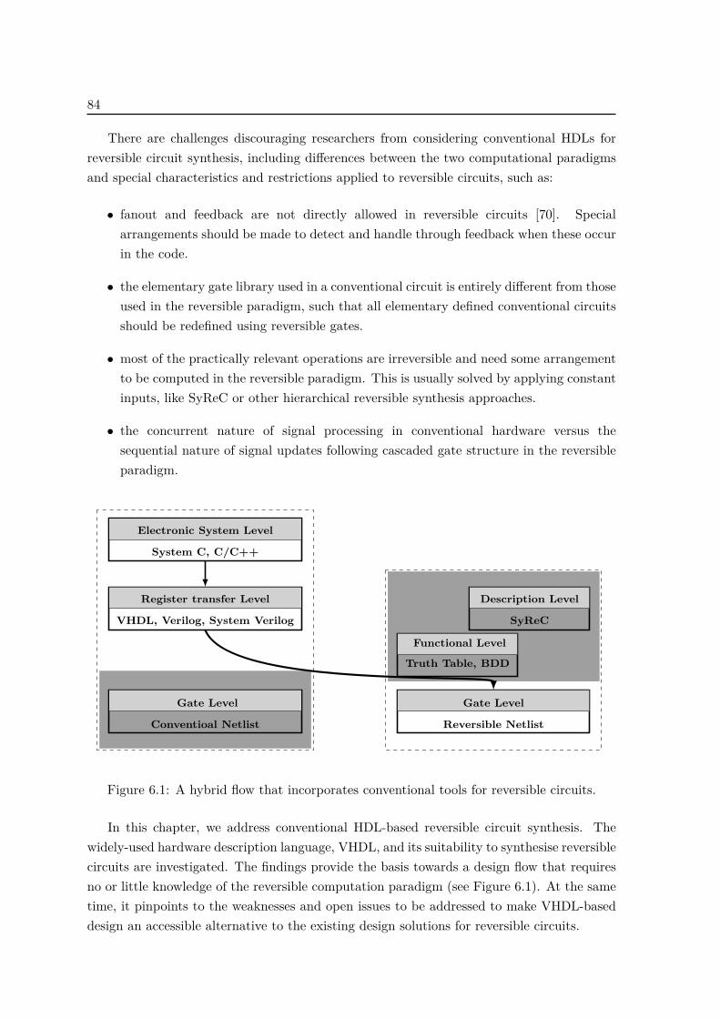
84
There are challenges discouraging researchers from considering conventional HDLs forreversible circuit synthesis, including differences between the two computational paradigmsand special characteristics and restrictions applied to reversible circuits, such as:
• fanout and feedback are not directly allowed in reversible circuits [70]. Specialarrangements should be made to detect and handle through feedback when these occurin the code.
• the elementary gate library used in a conventional circuit is entirely different from thoseused in the reversible paradigm, such that all elementary defined conventional circuitsshould be redefined using reversible gates.
• most of the practically relevant operations are irreversible and need some arrangementto be computed in the reversible paradigm. This is usually solved by applying constantinputs, like SyReC or other hierarchical reversible synthesis approaches.
• the concurrent nature of signal processing in conventional hardware versus thesequential nature of signal updates following cascaded gate structure in the reversibleparadigm.
Register transfer Level
VHDL, Verilog, System Verilog
Gate Level
Conventioal Netlist
Electronic System Level
System C, C/C++
Functional Level
Truth Table, BDD
Gate Level
Reversible Netlist
Description Level
SyReC
Figure 6.1: A hybrid flow that incorporates conventional tools for reversible circuits.
In this chapter, we address conventional HDL-based reversible circuit synthesis. Thewidely-used hardware description language, VHDL, and its suitability to synthesise reversiblecircuits are investigated. The findings provide the basis towards a design flow that requiresno or little knowledge of the reversible computation paradigm (see Figure 6.1). At the sametime, it pinpoints to the weaknesses and open issues to be addressed to make VHDL-baseddesign an accessible alternative to the existing design solutions for reversible circuits.

6. Synthesis of Reversible Circuits Using Conventional HDL 85
6.1 Introducing VHDL
VHDL is a hardware description language designed to allow for the description of thestructure of a circuit, i.e., its decomposition into subsystems as well as the interconnections,by utilising an established programming style and different levels of abstractions. UsingVHDL, circuits can be simulated, synthesised, and verified before being manufactured [18].More precisely, a circuit is first defined by an entity declaration, which introduces a namefor the entity and lists the ports (input and output signals). An entity declaration describesthe external view of the design.
The internal implementation of an entity is provided in an architecture body of thatentity. Architectures might be provided in different fashions. A behavioural architecturebody describes the function in an abstract way, e.g., in terms of process statements. A processstatement defines a sequence of operations to be executed when the circuit is simulated. Awide variety of actions might be included within a process statement, which, in some cases,restricts the synthesis of the architecture.
Synthesis-oriented programmers prefer an alternative model to describe theimplementation of an entity, which is called structural description. This model describesthe circuit in terms of a net-list of sub-circuits. More precisely, sub-circuits are declaredas components. Multiple component instances (i.e., copies) may appear in the architecturebody to represent these subsystems. A component instance includes a port map to specifythe interconnections of these component instances within the enclosed architecture body.
1 entity main is2 port( q,r,s: in bit; y: out bit);3 end entity main;4
5 architecture structural of main is6 component sub is7 port(a,b: in bit; f: out bit);8 end component sub;9 signal t: bit;
10 begin11 L1: test port map (a => q, b => r, f => t)12 L2: test port map (a => t, b => s, f => y);13 end architecture structural;
Figure 6.2: Structural VHDL architecture.
Another possible description used signal assignment statements, which define the flow ofdata to compute signals. An architecture body described completely using signal assignmentstatements is typically referred to as a data-flow description style. Often it is useful todescribe the required system using a mixture of processes, interconnected components, andsignal assignment statements.

86 VHDL Signals in Reversible Circuits
In the remainder of this chapter, we focus on the main descriptions provided by VHDLto utilise reversible circuit synthesis. Simulation related descriptions, including processstatement actions, are not covered. Because feedback connections are not allowed in thereversible circuit paradigm, circuits that contain feedback are also not supported.
1 entity sub is2 port (a,b: in bit; f: out bit);3 end entity test;4
5 architecture data_flow of test is6 signal x: bit;7 begin8 S1: x <= not b;9 S2: f <= a and x;
10 end architecture data_flow;
Figure 6.3: Data-flow in VHDL architecture.
Example 32. Figure 6.3 provides an example of a data-flow VHDL circuit. The entitynamed sub has three single-bit ports, namely two input ports (a,b) and one output port (f).A single-bit wire signal (x) is declared within the architecture body. The implementation ofthis system contains two signal assignment statements. The first statement (S1) computes thewire signal x, while the second statement (S2) computes the output signal f. Figure 6.2, onthe other hand, shows a structural description of a VHDL architecture (main), in which theentity sub defined in Figure 6.3 is declared and instantiated twice (statements L1 and L2).The port map associated with each instance defines the inter-connectivity of this specificcomponent-instance within the main circuit.
6.2 VHDL Signals in Reversible Circuits
A VHDL signal is meant as a mathematical representation of a circuit node in conventionalhardware where the changing value of the signal (waveform) can be measured at any time.Circuit components should be properly interconnected to compute the desired signals todrive these nodes. This representation is no longer valid.
6.2.1 Circuit-lines of VHDL Signals
VHDL signal types can be mapped directly to signals (lines) of the reversible circuits.In Figure 6.3 we can see examples of different types of signals in a VHDL code, which aremapped to lines with different specifications as follows:
1. Input ports a,b: These lines carry input values to the circuit and remain unchangedwithin a circuit because such signals are only carrying information to the circuit froman external source of information.

6. Synthesis of Reversible Circuits Using Conventional HDL 87
2. Output port f : With a constant ′0′ input, an expression is assigned to this signal(line) by a statement within the architecture body.
3. Internal signal x : This line represents an internal wire. It is similar to output portsin that it is initially constant ′0′ and assigned in the same way. The difference betweenoutputs and wires is that wires facilitate computing other signal(s), and then thet areconsidered garbage outputs.
4. Implicit lines: These lines are similar to internal signals in that they have constant ′0′
inputs and constitute garbage outputs, but are not explicitly declared within the code.Such lines are mandatory to compute non-reversible operations, e.g., to compute theexpression (a and x) in Figure 6.3, Statement S2.
6.2.2 VHDL Signals versus SyReC Signals
Despite many similarities, signal types in VHDL differ from SyReC because each languageis oriented to describe a different circuit paradigm, including:
1. VHDL defines inout ports when a certain signal functions sometimes as an in andotherwise as an out, e.g., bidirectional data-bus signals. This has no relevance to theconcept of inout signals in SyReC where inout means simply a signal that is validat both ends of a circuit line. VHDL inout is not discussed in this context becauseit is related to state-dependent (sequential) digital systems, which contain feedbackbehaviour that is not allowed, by definition, in the reversible paradigm.
2. Multiple assignments to a signal cause a conflict in a conventional paradigm becauseit merely means connecting the outputs of different gates. Consequently, any signal isassigned, at the most, just once within the architecture body.
3. Since in signals, in VHDL, are not updated within the architecture body, and remainunchanged at the output end, which is unlike in-type signals in SyReC, which areconsidered garbage because they can be updated, or changed, within the module.
4. Signal assignments applied only to signals form non-in types, which are known to beconstant ′0′. In other words, assignment of an expression to a signal does not causeany information loss.
Up to this point, the reversible circuit is composed of empty lines only without anygates. In other words, for a circuit with an identity function, realising a VHDL code doesnothing. Gates are added to process signals on circuit lines to compute the desired outputsas described by the statements in the architecture body.

88 Flow of Data with Signal-Assignment
6.3 Flow of Data with Signal-Assignment
An assignment statement, in its simplest form (S <= E;), is composed of three parts, atarget signal S, an assignment operator <= and a right-hand side expression E. To realise astatement, two steps are to be followed:
1. Compose a sub-circuit GE realising the expression E (see Section 6.3.1).
2. Use Toffoli gates to assign E to the target-signal to realise the overall statement(see Section 6.3.2).
6.3.1 Expressions
VHDL provides a set of operations, such as Boolean, arithmetic, and comparison. Theoperations are applied on operand signals to compose VHDL expressions. As much as itis considered in SyReC, most operations are irreversible. Hence, an additional line withconstant inputs is applied to make an irreversible function reversible [36] leading to theimplicit lines (discussed in Section 6.2). This is exactly how the reversible HDL SyReC tacklesthe problem [24]. In fact, most VHDL-defined operators can use circuit definitions providedfor equivalent operations in SyReC. Despite differences in the grammar, defined operations,and their precedence between the two languages, which imply some modifications, the ideasproposed to realise SyReC expressions are applicable, as well, to realise VHDL expressions(see Chapter 5). Again, realising an expression E which is combined with N operators willimplicitly add N constant lines to the circuit.
0 −
0 −
0 −
0 −
0 −
0 E
c c
b b
a a
l1
l2
l3
l4
l5
l6
l1
l2
l3
l4
l5
l6
andnot
and
or
not
xor
Figure 6.4: Circuit realising expression E from Example 33.
Example 33. Figure 6.4 shows a reversible circuit to compute the VHDL expression E, whichis given by (not(a and b) and c xor not(a or c)). The expression is computed based onsix Boolean operations. So, six constant input lines are applied to the circuit.

6. Synthesis of Reversible Circuits Using Conventional HDL 89
6.3.2 Assignment Operation
In contrast to SyReC, which has more than one operator to update signals reversibly,VHDL has only the signal-assignment operator, <=, that copies the line on the RHS to theLHS. A Toffoli gate can be used to copy the value of a line E into line S, if and only if, S isa constant ′0′, as shown in Figure 6.5(a), because ((E xor 0)=E). The operation is a simpleassignment (S <= E) by which the expression E as computed in Section 6.3.1, is assigned tothe target (non-input) signal S, which is known to be a constant ′0′ (see Section 6.2).
0 S
E E
(a) Simple
0 S
Ef Ef
Et Et
C C
(b) ConditionalS = 0 S
Cn Cn
C2 C2
C1 C1
Ed Ed
En En
E2 E2
E1 E1
(c) Multiple
Figure 6.5: Realisation of signal assignment.
Conditional signal assignments are also provided in VHDL, with the form(S <= Et when C else Ef), by which Et is assigned to the target signal S only when thecondition C is evaluated to ’true’ or ′1′, while Ef is assigned otherwise, as shown inFigure 6.5(b). A conditional assignment may be extended to multiple-conditionals(see Figure 6.15). A generalised arrangement of gate allows the realisation of such multipleconditional assignments, as shown in Figure 6.5(c).
6.4 Interconnecting Statements
An overall circuit realisation for a given VHDL code is computed by interconnectingsub-circuits together within one main circuit. This includes components’ instances in additionto the signal assignment statements.
6.4.1 Statement Cascade
A key difference between conventional and reversible circuit paradigms is addressed here.In conventional circuits, it does not matter which statement is realised first, as the result willbe the same hardware because of statement concurrency. A reversible computation paradigm,on the other hand, successively processes signals by cascaded gates. Consequently, signals are

90 Interconnecting Statements
successively (not concurrently) computed. In this regard, the order in which the statementsare considered has an effect.
Signals should be prioritised according to their dependence. In other words, a signalis computed only when its operand signals are available (either input or computed wires).Signal prioritisation may not be resolved if there exist two or more signals that depend oneach other. This cyclic dependence indicates feedback, which violates a basic principle inthe reversible paradigm.
0 −
0 −
x = 0 −
f = 0 f
b b
a a
GES1GES2
Figure 6.6: Reversible circuits realised using the VHDL code from Figure 6.3.
Example 34. The VHDL code in Figure 6.3 contains two assignment statements, whereeach statement has an expression with one operator on its RHS. Consequently, two implicitlines are expected. The resulting circuit is shown in Figure 6.6.a.
6.4.2 Components
As mentioned in Section 6.1, the structural style describes systems as a set ofinterconnected components. Components are entities instantiated within the architectureof another entity. Each instance places a sub-circuit definition within the main circuit.The reversible circuit of a component should be determined before interconnecting the maincircuit in which it is instantiated. The order of the signal lines in the component circuit maydiffer from the signals mapped to them in the main circuit. Hence, a port map is associatedwith each instance to serve as a look-up table for line mapping.
Example 35. Figure 6.2 shows a VHDL description of the entity main with a structuralarchitecture body, which declares a component, then instantiates it twice. The componentrefers to the entity sub, as described in Figure 6.3, with the circuit Gsub, as shown inFigure 6.6. The structural interconnection of the main circuit Gmain in Figure 6.7(a)follows the port map of each component instance to map the lines. This can be observedfrom Figure 6.7(b), where each instance sub-circuit is identical to the component circuit inFigure 6.6, but with lines rearranged according to the mapping of each instance. The circuitGmain is realised using 11 lines, 4 of which are ports (q, r, s, y), 1 internal signal t, and 6implicit lines.

6. Synthesis of Reversible Circuits Using Conventional HDL 91
0 -
r rq q
s s0 y
0 -
0 -
0 -
t
s
a
b
f a
b
fGsub
Gsub
Gmain
(a) Structural interconnection of components
rr
ssy0-0-0-0-0-0-0-0
t
a
b
x
b
a
x
f
f
(b) Circuit realisation on the gate level
Figure 6.7: The interconnecting structural VHDL architecture code from Figure 6.2.
6.5 Improving the Circuit Realisation
Expressions and other non-reversible actions implicitly add constant lines to the circuit.These lines are accumulated throughout statements and result in circuits with a large numberof constant inputs, e.g., more than half of the lines in the circuit Gmain computed inExample 35 are implicit. In this section, we propose line-aware arrangements to reducethe number of lines and gate costs.
0 0
x = 0 −
f = 0 f
b b
a a
GES1 G−1ES1
GES2 G−1ES2
Figure 6.8: Reversible circuit realised using the VHDL code from Figure 6.3.
6.5.1 Line-aware Synthesis
According to the interconnection suggested in Section 6.2.1, implicit lines are assigned andused only once within the architecture body the outputs are garbage, i.e., not usable againin the circuit. Realising a statement with no garbage is possible when the RHS expression iscomputed in the reverse direction (re-computed). This technique was proposed for line-awareSyReC synthesis (see Section 3.3.1). More precisely, in addition to the two steps fromSection 6.3, a third step is added:

92 Improving the Circuit Realisation
3. Add the inverse circuit, G−1E , to re-compute the garbage.
The next statement reuses the same lines to realise a circuit with fewer lines.
Example 36. Figure 6.8 shows the reversible circuit realisation for the VHDL code fromFigure 6.3 following this scheme. The circuit requires only 1 implicit line instead of 2 linesas in the circuit from Figure 6.6.
0 −
0 E
c c
b b
a a
l1
l2
0
Figure 6.9: Line-aware realising of expression E from Example 33.
The ideas to realise optimised expressions in SyReC as proposed in Chapter 5 areapplicable on VHDL by which expressions are computed with less constant inputs. Applyingthis optimised realisation on the expression from Example 33 results in the circuit shown inFigure 6.9, which is computed using 2 constant lines versus 6 in the direct realisation shownin Figure 6.4.
6.5.2 Gate-level Complexity Reduction
A constant input is not a signal fed into the circuit but it is like a literal numericvalue in the code. In the conventional realisation of VHDL codes, numbers (i.e., literals)do not require circuits to compute their values as they are already specified in the code.Furthermore, an operation on a number operand can dramatically reduce the complexity ofthe circuit.
In the reversible circuit paradigm, a number is represented as a constant input. Usinga constant input for each number in the code worsens the circuit parameters. On theother hand, considering constant signals, gate complexity may be reduced to lead towardsoptimised circuits1. This motivates exploiting the following two simple properties:
1. A control with a constant ′1′ may be removed from the gate.
2. A Toffoli gate with one control known to be constant ′0′ may be removed from thecircuit.
1If the operation is applied to all number operands, then the circuit will be reduced to a set of constantinputs, i.e., no circuit at all.

6. Synthesis of Reversible Circuits Using Conventional HDL 93
0 (op = v)
v.1 v.1
v.0 v.0
op.1 op.1
op.0 op.0
(a) (op = v) signal operand
0 (op = 3)
op.1 op.1
op.0 op.0
(b) (op = 3) number operand
0 (op = 1)
op.1 op.1
op.0 op.0
(c) (op = 1) number operand
0 (op = 0)
op.1 op.1
op.0 op.0
(d) (op = 0) number operand
Figure 6.10: Gate-level optimisation of constant input.
Example 37. Figure 6.10(a) shows the circuit of a 2-bit equality operation (op = v) whereop and v are both variables. In the VHDL code of Figure 6.15, we can see a special caseof this operation used as conditions, e.g., (op = 0). In this case, one of the operands isa constant number instead of a variable signal. Applying the complexity reduction rules, assuggested above, results in Figure 6.10(d), which uses fewer lines and has a lower gate cost.Applying the same optimisation on conditions with different numbers, such as (op = 3)
and (op = 1), results in a different circuits, e.g., Figures 6.10(b) and 6.10(c).
6.6 Discussion
This section discusses the resulting VHDL-based synthesis approach for reversible circuitsand compares it to the reversible-specific solution SyReC introduced in [24]. Between bothsolutions, one fundamental difference is the signal assignment, which is non-reversible inVHDL (<=, i.e., the previous signal value will be lost) and reversible in SyReC (ˆ=, i.e., byadditionally employing an XOR assignment, for example, which might require the additionof out and wire signals to realise the intended functionality). Also, the way to computeexpressions, conditionals, and components are very similar between VHDL and SyReC whenapplied to constant inputs.
In the following, we consider two cases to study how these differences (and also thesimilarities) may affect the respectively obtained synthesis result.

94 Discussion
6.6.1 Case Study: Gray-code to Binary-Code Conversion
Figure 6.11 shows a VHDL description2. of a 4-bit gray-code to binary code converter.The code defines two 4-bit vectors: (g) to the input gray-code and (b) for the output binarycode. The architecture description in this code incorporates some repeated computations,e.g., (g(3) xor g(2)) is computed three times. Hence, an equivalent description isproposed in Figure 6.12 to reduce the resulting computation complexity and the circuit cost.This code declares a 3-bit wire w to facilitate the computations. Despite being describedusing more statements, this code can be realised with reduced circuit costs, as shown inTable 6.1, which summarises the resulting circuit costs:
entity gray2binary isport (g : in STD_LOGIC_VECTOR (3 downto 0);
b : out STD_LOGIC_VECTOR (3 downto 0));end entity gray2binary;
architecture Behavioral of gray2binary isbegin
b(3) <= g(3);b(2) <= g(3) xor g(2);b(1) <= g(3) xor g(2) xor g(1);b(0) <= g(3) xor g(2) xor g(1) xor g(0);
end behavioral;
Figure 6.11: 4-bit gray-code to binary converter using VHDL.
1. for basic realisation, as described in Sections 6.3 and 6.4, with no optimisation. Thisrealisation results in lower gate count and cost, but with a larger number of lines.
2. for improved realisation as described in Section 6.5. This realisation shows higher gatecount and cost, but with fewer lines.
architecture Behavioral of gray2binary issignal w (2 downto 0);
beginw(2) <= g(3) xor g(2);w(1) <= w(2) xor g(1);w(0) <= w(1) xor g(0);b(3) <= g(3);b(2) <= w(2);b(1) <= w(1);b(0) <= w(0);
end architecture behavioral;
Figure 6.12: Optimized architecture description of Figure 6.11 to reduce complexity.
2This code is taken from http://www.rfwireless-world.com

6. Synthesis of Reversible Circuits Using Conventional HDL 95
We additionally consider a reversible HDL description, provided in SyReC syntax, as shownin Figure 6.13. This code conversion is reversible by definition, because of the one-to-onecorrespondence between the two codes. Hence, the gray-code to binary code converter is anideal example to demonstrate the merits of SyReC-based synthesis (in its current state ofdevelopment) compared to VHDL-based synthesis introduced above. The SyReC approachperforms significantly better because reversibility can fully be exploited.
module gray2binary(inout x(4))x.2 ˆ= x.3x.1 ˆ= x.2x.0 ˆ= x.1
Figure 6.13: Gray-code to binary code converter using SyReC.
Table 6.1: Experimental results of the 4-bit gray-code to binary code converter.
Parameter VHDL SyReCFigure 6.11 Figure 6.12 Figure 6.131 2 1 2
Gates 16 28 10 16 3Total lines 14 11 11 9 4
Quantum cost 16 28 10 16 3Transistor cost 128 224 80 128 24
6.6.2 Case Study: Logic Unit
As another example, we consider a case where non-reversible functionality should berealised. Figures 6.14 and 6.15 show two equivalent codes describing a 32-bit logic-unitdescribed in SyReC3 and VHDL, respectively. A conditional assignment computes theoutput signal x0. In the SyReC code, x0 is initialized using the XOR-operator (ˆ=), e.g., inx0 ˆ= (x1 & x2). Here, the operation is identical to (<=) in VHDL since x0 is an out
signal.For the SyReC code, the circuit is realised in four different configurations as summarised
in Table 5.1, namely:
1. The basic SyReC synthesis: incorporates no optimisation and results in a low gatecount [24].
2. The line-aware synthesis: implements statement re-compute and reuses circuit linesand exploits fewer lines [62].
3. The cost-aware synthesis: exploits an extra (helper) line to reduce gates cost, and thisconfiguration shows lower cost measures [42].
3A SyReC benchmark (lu 238.src) in RevLib [67].
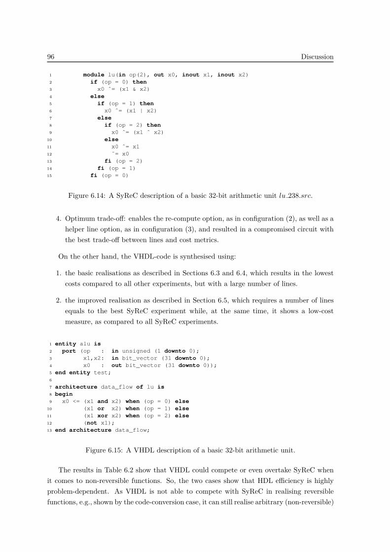
96 Discussion
1 module lu(in op(2), out x0, inout x1, inout x2)2 if (op = 0) then3 x0 ˆ= (x1 & x2)4 else5 if (op = 1) then6 x0 ˆ= (x1 | x2)7 else8 if (op = 2) then9 x0 ˆ= (x1 ˆ x2)
10 else11 x0 ˆ= x112 ˜= x013 fi (op = 2)14 fi (op = 1)15 fi (op = 0)
Figure 6.14: A SyReC description of a basic 32-bit arithmetic unit lu 238.src.
4. Optimum trade-off: enables the re-compute option, as in configuration (2), as well as ahelper line option, as in configuration (3), and resulted in a compromised circuit withthe best trade-off between lines and cost metrics.
On the other hand, the VHDL-code is synthesised using:
1. the basic realisations as described in Sections 6.3 and 6.4, which results in the lowestcosts compared to all other experiments, but with a large number of lines.
2. the improved realisation as described in Section 6.5, which requires a number of linesequals to the best SyReC experiment while, at the same time, it shows a low-costmeasure, as compared to all SyReC experiments.
1 entity alu is2 port (op : in unsigned (1 downto 0);3 x1,x2: in bit_vector (31 downto 0);4 x0 : out bit_vector (31 downto 0));5 end entity test;6
7 architecture data_flow of lu is8 begin9 x0 <= (x1 and x2) when (op = 0) else
10 (x1 or x2) when (op = 1) else11 (x1 xor x2) when (op = 2) else12 (not x1);13 end architecture data_flow;
Figure 6.15: A VHDL description of a basic 32-bit arithmetic unit.
The results in Table 6.2 show that VHDL could compete or even overtake SyReC whenit comes to non-reversible functions. So, the two cases show that HDL efficiency is highlyproblem-dependent. As VHDL is not able to compete with SyReC in realising reversiblefunctions, e.g., shown by the code-conversion case, it can still realise arbitrary (non-reversible)

6. Synthesis of Reversible Circuits Using Conventional HDL 97
functions with comparable or even better circuits, e.g., as shown by the logic-unit case.In either case, VHDL is more convenient for designers with no or little knowledge of thereversible computation paradigm.
Table 6.2: Experimental results of a 32-bit logic unit.
Parameter SyReC VHDL1 2 3 4 1 2
Gates 384 612 392 622 414 671Total lines 197 133 198 134 235 133
Quantum cost 6557 10462 2312 3894 682 1207Transistor cost 9856 15616 6360 10288 3472 5752
6.7 Summary
In this chapter, we considered a conventional hardware description language (VHDL) torealise reversible circuits. The structural description model is analysed and direct realisationsfor signals, expressions, assignments, conditionals, and components are proposed.
Optimised realisations are also proposed for higher quality circuits, including a line-awaresynthesis and a complexity reduction arrangement. The differences and similarities werediscussed as compared to the dedicated reversible HDL (SyReC). The discussion shows thateach approach has some advantages and declaring a winner depends on the problem to bedescribed.
The chapter provides an elementary basis towards a conventional HDL-based reversiblecircuit design, with only a little knowledge for the programmer in this computationalparadigm.


99
Chapter 7
Improving the Grammar of SyReC
To be accepted as a first-choice tool for reversible circuit design, SyReC programmingshould be convenient for a wide range of programmers along with its scalability, modularity,and the quality of its circuits. The previous efforts invested in improving the SyReC designapproach were focused on synthesis-related issues aimed a realising higher-quality circuits.So, language’s grammar has not been revised since its first release in 2010 [61]. With ourexperience in SyReC programming, we highlight possible enhancements and extensions tothe grammar of this HDL to make the language more powerful and more convenient as well.In this chapter, we propose grammatical extensions to SyReC by appending some syntacticalrules, modifying others, and defining more data operations.
7.1 Control Logic
To guarantee reversibility of the descriptions of SyReC, a reversible control flow isimplemented [24]. Consequently, conditional statements do require not only an if-condition(to decide which of the then- or the else-block is to be executed next) but also a fi-condition(for the same reason, if the computation is conducted in reverse direction). This was firstintroduced in the reversible software language Janus [64], where the fi-condition is called anassertion. So, SyReC, which is based on Janus, inherited this assertion. Moreover, HDLdescriptions do occur from which it is not possible to realise a reversible control flow. Hence,designers of reversible circuits and systems are faced with the problem of properly describinga reversible control flow and the uncertainty whether such a control flow is even possible.With this violation, it is not apparent whether the entire SyReC description is fully reversible.
Example 38. The if-condition of the Figure 7.1(a) is (a = 5) and the signal a is notupdated within the statement. Therefore the same expression is valid as a fi-condition andthe statement is fully reversible. On the other hand, the if-condition in Figure 7.1(b) is(x = y). Here, the signals used to compute the expression are updated within the statement,and so the same expression is no longer a valid fi-condition. To incorporate signal updates,a correspondingly adjusted fi-condition is required, ((x - 1) = y) in this case. This
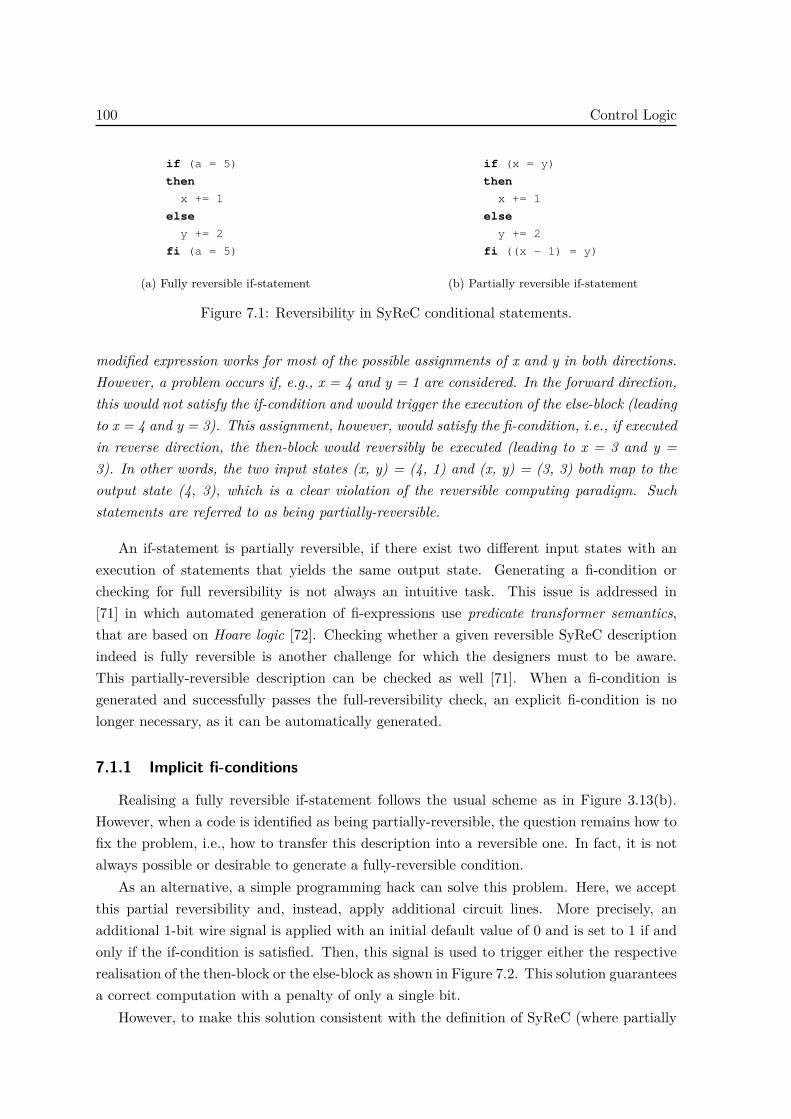
100 Control Logic
if (a = 5)
then
x += 1
else
y += 2
fi (a = 5)
(a) Fully reversible if-statement
if (x = y)
then
x += 1
else
y += 2
fi ((x - 1) = y)
(b) Partially reversible if-statement
Figure 7.1: Reversibility in SyReC conditional statements.
modified expression works for most of the possible assignments of x and y in both directions.However, a problem occurs if, e.g., x = 4 and y = 1 are considered. In the forward direction,this would not satisfy the if-condition and would trigger the execution of the else-block (leadingto x = 4 and y = 3). This assignment, however, would satisfy the fi-condition, i.e., if executedin reverse direction, the then-block would reversibly be executed (leading to x = 3 and y =3). In other words, the two input states (x, y) = (4, 1) and (x, y) = (3, 3) both map to theoutput state (4, 3), which is a clear violation of the reversible computing paradigm. Suchstatements are referred to as being partially-reversible.
An if-statement is partially reversible, if there exist two different input states with anexecution of statements that yields the same output state. Generating a fi-condition orchecking for full reversibility is not always an intuitive task. This issue is addressed in[71] in which automated generation of fi-expressions use predicate transformer semantics,that are based on Hoare logic [72]. Checking whether a given reversible SyReC descriptionindeed is fully reversible is another challenge for which the designers must to be aware.This partially-reversible description can be checked as well [71]. When a fi-condition isgenerated and successfully passes the full-reversibility check, an explicit fi-condition is nolonger necessary, as it can be automatically generated.
7.1.1 Implicit fi-conditions
Realising a fully reversible if-statement follows the usual scheme as in Figure 3.13(b).However, when a code is identified as being partially-reversible, the question remains how tofix the problem, i.e., how to transfer this description into a reversible one. In fact, it is notalways possible or desirable to generate a fully-reversible condition.
As an alternative, a simple programming hack can solve this problem. Here, we acceptthis partial reversibility and, instead, apply additional circuit lines. More precisely, anadditional 1-bit wire signal is applied with an initial default value of 0 and is set to 1 if andonly if the if-condition is satisfied. Then, this signal is used to trigger either the respectiverealisation of the then-block or the else-block as shown in Figure 7.2. This solution guaranteesa correct computation with a penalty of only a single bit.
However, to make this solution consistent with the definition of SyReC (where partially

7. Improving the Grammar of SyReC 101
wire w(1)
if (x = y)
then
x += 1
˜=w
else
y += 2
fi w
(a) fi-condition using a wire
0 0Gif
x x′
y y′
⊕=
Gthen ⊕=
Gelse
w = 0 −
(b) Realisaion of a partially-reversible fi-condition
Figure 7.2: Fully-reversible fi-condition using an internal wire.
reversible descriptions are not allowed), we must modify the grammar. In fact, we simplymake the fi-condition optional as shown in Figure 7.8 (line 12). Whenever the fi-condition isprovided, a synthesiser simply realises the corresponding expression. Whenever the conditionis omitted, a synthesiser uses the algorithms proposed in [71] to generate a suitable fi-condition.If this is possible (i.e., the conditional statement is fully-reversible), then the resultingfi-condition is realised. Otherwise, a single bit wire is automatically declared and applied asdescribed above.
7.1.2 Reversible Case-statement
Considering the same approach in dealing with fi-conditions, other control statements canbe proposed, and a reversible case-statement is now possible to be realized. Case-statementsrepresent a special form to represent nested if-statement structures where all if-conditionshave the same form (choice_expression = <number>). Instead of repeating thechoice expression with each if-condition, it is provided once at the beginning of the casestatement. This will tangibly enhance the readability of the code and simplify the structure.It is an intuitive task to map these case-statements into equivalent nested-if structures anddoes not constitute a serious obstacle for the synthesis process. Overall, this motivatesextensions to the SyReC grammar as shown in Figure 7.8 (lines 28 and 30).
Example 39. Figures 7.3(a) and 7.3(b) show two equivalent SyReC specifications wherethe former is written using the original SyReC grammar (i.e., as a cascade of conditionalstatements) and the latter is written using the proposed case statement.
7.2 Data Operations
Reversible HDLs are supposed to facilitate the description of reversible circuits. Thisincludes a complete set of defined data-operations. The current version of SyReC alreadyprovides many data operations, but misses essential operations such as bit-wise rotationoperations, which is a defined operation in other HDLs, such as VHDL. The operation is

102 Data Operations
1 module simple_alu(in op(2), in a, in b, out c)
2 if (op = 0)
3 then
4 c ˆ= (a + b)
5 else
6 if (op = 1)
7 then
8 c ˆ= (a - b)
9 else
10 if (op = 2)
11 then
12 c ˆ= (a * b)
13 else
14 c ˆ= (a / b)
15 fi (op = 2)
16 fi (op = 1)
17 fi (op = 0)
(a) Nested if-fi code
1 module simple_alu(in op(2), in a, in b, out c)
2 with op select
3 case 0: c ˆ= (a + b)
4 case 1: c ˆ= (a - b)
5 case 2: c ˆ= (a * b)
6 case default: c ˆ= (a / b)
7 endcase
(b) Reversible case statement
Figure 7.3: SyReC description of a simple arithmetic unit.
obviously reversible, and it receives special significance in cyclic-coding applications andcryptography [73].
In the original grammar of SyReC, programmers needed to write a sophisticated code toperform a rotation operation bit-by-bit. To accomplish this, they could use the related shiftoperators << and >> or XOR assignment statements ˆ=, which are not reversible and requireadditional circuit lines. This is not only counter-intuitive and against the aim of facilitatingthe design process, but also yields significantly larger circuits.
Example 40. Figure 7.4 shows a SyReC code to update the 8-bit signal y using the ˆ=
operator. The value of signal x is rotated 3-bits to the left of the bit-wise and XOR-ed withy. This code shows that the operation is defined bit-by-bit. The resulting code is not intuitive.Moreover, the circuit is large due to the need to embed this shift operation with an additionalsignal x (see Figure 7.4(b)).
SyReC grammar is extended such that bit-wise rotation is incorporated. The operations<| and |> are defined for rotate-left and rotate-right, respectively. Accordingly, the rotation
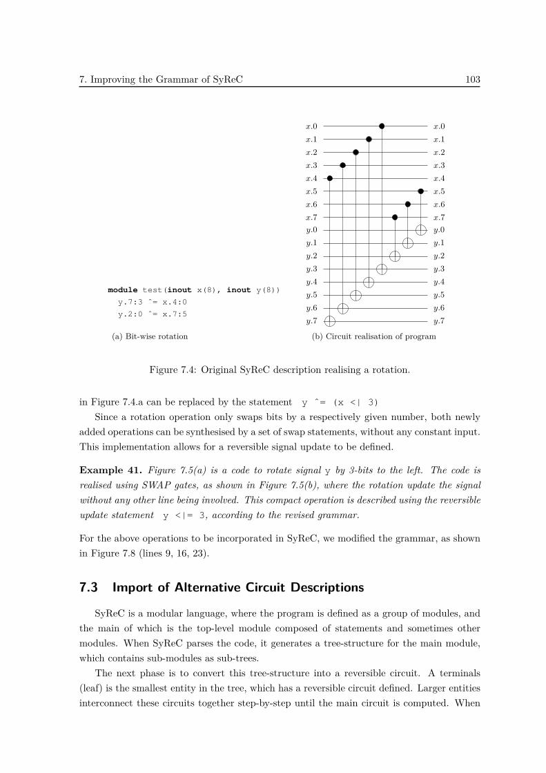
7. Improving the Grammar of SyReC 103
module test(inout x(8), inout y(8))
y.7:3 ˆ= x.4:0
y.2:0 ˆ= x.7:5
(a) Bit-wise rotation
x.0 x.0x.1 x.1x.2 x.2x.3 x.3x.4 x.4x.5 x.5x.6 x.6x.7 x.7y.0 y.0y.1 y.1y.2 y.2y.3 y.3y.4 y.4y.5 y.5y.6 y.6y.7 y.7
(b) Circuit realisation of program
Figure 7.4: Original SyReC description realising a rotation.
in Figure 7.4.a can be replaced by the statement y ˆ= (x <| 3)
Since a rotation operation only swaps bits by a respectively given number, both newlyadded operations can be synthesised by a set of swap statements, without any constant input.This implementation allows for a reversible signal update to be defined.
Example 41. Figure 7.5(a) is a code to rotate signal y by 3-bits to the left. The code isrealised using SWAP gates, as shown in Figure 7.5(b), where the rotation update the signalwithout any other line being involved. This compact operation is described using the reversibleupdate statement y <|= 3, according to the revised grammar.
For the above operations to be incorporated in SyReC, we modified the grammar, as shownin Figure 7.8 (lines 9, 16, 23).
7.3 Import of Alternative Circuit Descriptions
SyReC is a modular language, where the program is defined as a group of modules, andthe main of which is the top-level module composed of statements and sometimes othermodules. When SyReC parses the code, it generates a tree-structure for the main module,which contains sub-modules as sub-trees.
The next phase is to convert this tree-structure into a reversible circuit. A terminals(leaf) is the smallest entity in the tree, which has a reversible circuit defined. Larger entitiesinterconnect these circuits together step-by-step until the main circuit is computed. When

104 Import of Alternative Circuit Descriptions
module test(inout x(8), inout y(8))
y.7:3 <=> y.4:0
y.2:1 <=> y.1:0
(a) Bit-wise rotation
y.0 y.0y.1 y.1y.2 y.2y.3 y.3y.4 y.4y.5 y.5y.6 y.6y.7 y.7×
×
×
×
×
×
×
×
×
×
××××
(b) Circuit realisation
Figure 7.5: SyReC description realizing of a signal rotation.
module sub_circuit(inout a(1), inout b(1), out f(1))
wire w(1)
f ˆ= (a & b)
w ˆ= (a | b)
w <=> b
module main(inout x(1), inout y(1))
wire g(1)
call sub_circuit(x,y,g)
x <=> g
(a) Multiple module code
x (x & y)
y (x | y)
0g f −
0w −
0 −
0 −
×
××
×
(b) Reversible circuit realisation
Figure 7.6: SyReC description with sub-modules.
a module is called by another module (main), its circuit must be computed first; then it isused to compute the main circuit.
Example 42. Consider Figure 7.6(a), which shows a SyReC program composed of twomodules main and sub_circuit. The first is the top-level module that calls the laterin line 9 using a call statement. Applying the synthesis method, this yields the circuit asshown the bottom of Figure 7.6(b).
This modularity has only been used to call circuit descriptions provided in the SyReClanguage itself. However, we may have better circuits than those generated by SyReCsynthesised using different methodologies, but the current version of SyReC cannot use suchcircuits. This frequently prevents the realisation of more compact circuits because oftencheaper building blocks can not be described in SyReC, but only in terms of gate leveldescriptions.
To avoid this problem, we propose an extension to support the import of alternativecircuit descriptions (as an example, circuits described in the (.real) file format as introducedin [67] are considered). So, we extend the grammar from Figure 3.1 by allowing an<import-list> as defined in Figure 7.8 (lines 1, 2, and 29). This arrangement does

7. Improving the Grammar of SyReC 105
not require additional complexity to the circuit synthesis as it simplifies the computationsince some parts of the circuit are already determined, and all we need is into substitute(interconnect) them in the main circuit.
import sub_circuit from circuit_file.real
module main(inout x(1), inout y(1))
wire g(1)
call sub_circuit(x,y,g)
x <=> g
(a) SyReC program with circuit import
x (x & y)
y (x | y)
0 −g f ×
×
(b) Reversible circuit realisation
# ----- circuit_file.real ------
# This file has been generated using
# RevKit 1.3-snapshot (www.revkit.org)
.version 2.0
.numvars 3
.variables x0 x1 x2
.inputs a b const_0
.outputs a b f
.constants --0
.garbage --1
.begin
t3 x0 x1 x2
t3 x0 x2 x1
t2 x0 x1
.end
(c) Circuit netlist(.real file format)
Figure 7.7: SyReC description and realisation with imported circuit.
Example 43. Figure 7.7(a) shows a circuit description which is functionally equivalentto the description considered before in Figure 7.6(a). However, instead of describing theSyReC module sub_circuit, the corresponding reversible circuit is provided as shown inFigure 7.7(b)1 and imported using the newly-added statement (line 1). Overall, this yields asignificantly smaller circuit as shown in Figure 7.7(c).
According to the concept of modularity, which is based on information hiding, the detailsof each module are irrelevant to the other modules. Consequently, importing circuits is notsupposed to change the call statement, so it does not have any effect on the code of the mainmodule. However, because the functions of imported circuits are not explicitly described inthe code, it is necessary to verify the signal definition before importing a circuit. Specifically,it is important to verify that input and output specifications of the imported circuit match thecorresponding signals in the SyReC module, e.g., constant inputs and bit-widths of signals ,
1RevLib uses the (.real) file format to save netlists of reversible circuits [67].

106 Summary
for which it would be more convenient to import entities described using another HDL, suchas VHDL, that utilises port maps to explicitly specify signal types and bit-widths. With thismodification it becomes possible to achieve a hybrid HDL specification described using bothSyReC and VHDL, where SyReC modules call VHDL entities.
7.4 Summary
In this chapter, SyReC grammar is revised for the first time. The original grammarcauses several shortcomings making it harder to describe the desired behaviour and oftenyields more expensive circuits. These shortcomings are introduced with extensions to thelanguage and a proposed revised grammar (shown in Figure 7.8) that includes:
1. solving possible violations of full reversibility caused by fi-conditions in someif-then-else-fi statements (known as partial reversibility). Moreover, the proposedrealisation of partially-reversible statements allows for a reversible case statement.Both modifications simplify the grammar for more convenient SyReC programming.
2. defining new operations on data, such as a bit-wise rotation, which is a reversibleoperation. Hence, the modified grammar defines these operations within expressionsand as a reversible signal update statement.
3. enabling hybrid design by reusing circuit definitions, synthesised possibly usingmethodologies other than SyReC. The required circuits are imported and thenconnected to the main circuit using a normal call statement. This opens a door forthe integration of different methodologies within one design flow, which can result incircuits with higher qualities.
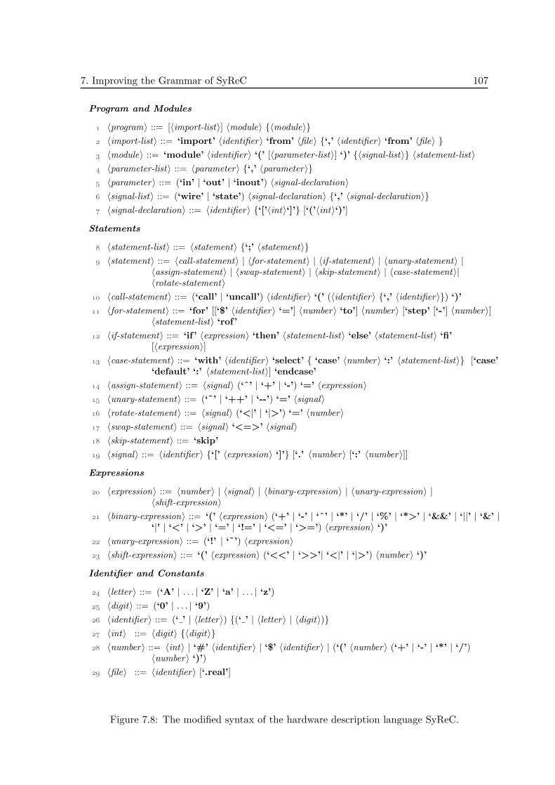
7. Improving the Grammar of SyReC 107
Program and Modules
〈program〉 ::= [〈import-list〉] 〈module〉 {〈module〉} 〈import-list〉 ::= ‘import’ 〈identifier〉 ‘from’ 〈file〉 {‘,’ 〈identifier〉 ‘from’ 〈file〉 } 〈module〉 ::= ‘module’ 〈identifier〉 ‘(’ [〈parameter-list〉] ‘)’ {〈signal-list〉} 〈statement-list〉 〈parameter-list〉 ::= 〈parameter〉 {‘,’ 〈parameter〉} 〈parameter〉 ::= (‘in’ | ‘out’ | ‘inout’) 〈signal-declaration〉 〈signal-list〉 ::= (‘wire’ | ‘state’) 〈signal-declaration〉 {‘,’ 〈signal-declaration〉} 〈signal-declaration〉 ::= 〈identifier〉 {‘[’〈int〉‘]’} [‘(’〈int〉‘)’]
Statements
〈statement-list〉 ::= 〈statement〉 {‘;’ 〈statement〉} 〈statement〉 ::= 〈call-statement〉 | 〈for-statement〉 | 〈if-statement〉 | 〈unary-statement〉 |
〈assign-statement〉 | 〈swap-statement〉 | 〈skip-statement〉 | 〈case-statement〉|〈rotate-statement〉
〈call-statement〉 ::= (‘call’ | ‘uncall’) 〈identifier〉 ‘(’ (〈identifier〉 {‘,’ 〈identifier〉}) ‘)’
〈for-statement〉 ::= ‘for’ [[‘$’ 〈identifier〉 ‘=’] 〈number〉 ‘to’] 〈number〉 [‘step’ [‘-’] 〈number〉]〈statement-list〉 ‘rof’
〈if-statement〉 ::= ‘if ’ 〈expression〉 ‘then’ 〈statement-list〉 ‘else’ 〈statement-list〉 ‘fi’[〈expression〉]
〈case-statement〉 ::= ‘with’ 〈identifier〉 ‘select’ { ‘case’ 〈number〉 ‘:’ 〈statement-list〉} [‘case’‘default’ ‘:’ 〈statement-list〉] ‘endcase’
〈assign-statement〉 ::= 〈signal〉 (‘ˆ’ | ‘+’ | ‘-’) ‘=’ 〈expression〉 〈unary-statement〉 ::= (‘˜’ | ‘++’ | ‘--’) ‘=’ 〈signal〉 〈rotate-statement〉 ::= 〈signal〉 (‘<|’ | ‘|>’) ‘=’ 〈number〉 〈swap-statement〉 ::= 〈signal〉 ‘<=>’ 〈signal〉 〈skip-statement〉 ::= ‘skip’
〈signal〉 ::= 〈identifier〉 {‘[’ 〈expression〉 ‘]’} [‘.’ 〈number〉 [‘:’ 〈number〉]]
Expressions
〈expression〉 ::= 〈number〉 | 〈signal〉 | 〈binary-expression〉 | 〈unary-expression〉 |〈shift-expression〉
〈binary-expression〉 ::= ‘(’ 〈expression〉 (‘+’ | ‘-’ | ‘ˆ’ | ‘*’ | ‘/’ | ‘%’ | ‘*>’ | ‘&&’ | ‘||’ | ‘&’ |‘|’ | ‘<’ | ‘>’ | ‘=’ | ‘!=’ | ‘<=’ | ‘>=’) 〈expression〉 ‘)’
〈unary-expression〉 ::= (‘!’ | ‘˜’) 〈expression〉 〈shift-expression〉 ::= ‘(’ 〈expression〉 (‘<<’ | ‘>>’| ‘<|’ | ‘|>’) 〈number〉 ‘)’
Identifier and Constants
〈letter〉 ::= (‘A’ | . . . | ‘Z’ | ‘a’ | . . . | ‘z’)
〈digit〉 ::= (‘0’ | . . . | ‘9’)
〈identifier〉 ::= (‘ ’ | 〈letter〉) {(‘ ’ | 〈letter〉 | 〈digit〉)} 〈int〉 ::= 〈digit〉 {〈digit〉} 〈number〉 ::= 〈int〉 | ‘#’ 〈identifier〉 | ‘$’ 〈identifier〉 | (‘(’ 〈number〉 (‘+’ | ‘-’ | ‘*’ | ‘/’)
〈number〉 ‘)’)
〈file〉 ::= 〈identifier〉 [‘.real’]
Figure 7.8: The modified syntax of the hardware description language SyReC.

109
Chapter 8
Conclusions
The traditional technology of computing machines developed over the last decades isabout to reach its limits. Consequently, an alternative paradigm needs to evolve sooner toreplace the conventional paradigm. Reversible computation may provide such an alternativereplacement or, at least, an enhancement of computing machines. Reversible logic ishighly-relevant to some interesting applications, such as quantum computing, low-powerdesign, adiabatic circuits, and encoding and decoding devices.
Different methodologies were proposed to realise functions as reversible circuits. Mostdo not scale well, i.e., they are not capable of handling large design problems. One approachto achieve scalability through hardware description languages, which are corner stones ofthe design flow of conventional circuits. Similarly, the HDL approach is also considered forreversible circuit design. A dedicated HDL, SyReC, is introduced for describing reversiblecircuits, and it shows the capacity to describe, with simple codes, relatively large designproblems, which are beyond the capacity of any other approach. The major drawback ofSyReC is that it realises reversible circuits with a large number of lines.
In this dissertation, an HDL-based design approach is optimised to generate reversiblecircuits with fewer lines. This includes improvements at different design levels, which aremade without compromising the advantages of the design approach, i.e., scalability andsimplicity.
The first improvement described in Chapter 4, is made on the programming style ofSyReC. Programmers, which are typically influenced by the conventional description style,deal with different paradigm considerations. The synthesis flow was investigated, and rulesfor SyReC programming with more efficiency are proposed resulting in circuits that aresynthesized with tangibly better metrics. However, SyReC codes written according to theproposed style are still less readable as compared to the spontaneous style.
In Chapter 5 we introduce line-aware realisations of SyReC expressions with which weavoid rewriting codes according to a certain programming style. Expressions in SyReC do notassume operations are reversible, so the realisations of these expressions follow conventionalcomputations. We exploit properties of reversible computations in realising circuits withbetter metrics for SyReC expressions. The fact that expressions in SyReC are not assuming

110
reversibility at all in its operations makes the concept introduced in this chapter applicablefor SyReC expressions as well as in conventional HDLs.
In Chapter 6 we investigate the conventional hardware description language, VHDL.We propose realisations of structural descriptions for architectures of entities in VHDL tointroduce a basis for a design flow that reuses elaborated conventional circuit design flow andits efficient tools and requires less knowledge in reversible paradigm. This may encouragestakeholders to accept reversible circuits as a practical alternative.
In Chapter 7 we propose some syntactical modifications on SyReC grammar includingnew control statements and definitions of new operations. Another modification allowsSyReC to import circuits that are designed using different methods and integrate themwithin the modules. This enables a hybrid design that profits from the advantages of eachapproach.
Finally, HDL-based design of reversible circuits cannot achieve synthesis with minimallines, but it can at least approach this goal within the scope of this dissertation. Also,reaching a thorough design flow for a reversible circuit, which can be considered as a practicalalternative, needs additional time to be well-established. Upcoming challenges are expected,and more effort is required. This dissertation contributes as an important step towards anelaborated design flow of reversible circuits.

111
Bibliography
[1] G. E. Moore, “Cramming more components onto integrated circuits,” Electronics,vol. 38, no. 8, pp. 114–117, 1965.
[2] C. H. Bennett, “Logical reversibility of computation,” IBM J. Res. Dev, vol. 17, no. 6,pp. 525–532, 1973.
[3] V. V. Shende, A. K. Prasad, I. L. Markov, and J. P. Hayes, “Synthesis of reversible logiccircuits,” IEEE Trans. on CAD, vol. 22, no. 6, pp. 710–722, 2003.
[4] D. Große, R. Wille, G. W. Dueck, and R. Drechsler, “Exact multiple control Toffolinetwork synthesis with SAT techniques,” IEEE Trans. on CAD, vol. 28, no. 5,pp. 703–715, 2009.
[5] R. Wille and R. Drechsler, “Synthesizing reversible logic: An overview,” in Int’lWorkshop on Applications of the Reed-Muller Expansion in Circuit Design, pp. 79–86,2009.
[6] N. Abdessaied and R. Drechsler, Reversible and Quantum Circuits Optimization andComplexity Analysis. Springer, 2016.
[7] G. F. Viamontes, M. Rajagopalan, I. L. Markov, and J. P. Hayes, “Gate-level simulationof quantum circuits,” in ASP Design Automation Conf., pp. 295–301, 2003.
[8] R. Wille, D. Große, D. M. Miller, and R. Drechsler, “Equivalence checking of reversiblecircuits,” in Int’l Symp. on Multi-Valued Logic, pp. 324–330, 2009.
[9] R. Landauer, “Irreversibility and heat generation in the computing process,” IBMjournal of research and development, vol. 5, no. 3, pp. 183–191, 1961.
[10] A. Berut, A. Arakelyan, A. Petrosyan, S. Ciliberto, R. Dillenschneider, andE. Lutz, “Experimental verification of Landauer’s principle linking information andthermodynamics,” Nature, vol. 483, pp. 187–189, 2012.
[11] B. Desoete and A. D. Vos, “A reversible carry-look-ahead adder using control gates,”INTEGRATION, the VLSI Jour., vol. 33, no. 1-2, pp. 89–104, 2002.
[12] P. Patra and D. Fussell, “On efficient adiabatic design of MOS circuits,” in Workshopon Physics and Computation, (Boston), pp. 260–269, 1996.

112 BIBLIOGRAPHY
[13] R. Wille, R. Drechsler, C. Oswald, and A. Garcia-Ortiz, “Automatic design of low-powerencoders using reversible circuit synthesis,” in Proceedings of the Conference on Design,Automation and Test in Europe, pp. 1036–1041, EDA Consortium, 2012.
[14] M. Nielsen and I. Chuang, Quantum Computation and Quantum Information.Cambridge Univ. Press, 2000.
[15] R. Gluck and M. Kawabe, “A method for automatic program inversion based on LR(0)parsing,” Fundamenta Informaticae, vol. 66, pp. 367–395, 01 2005.
[16] S. Abramov and R. Gluck, “The universal resolving algorithm and its correctness:inverse computation in a functional language,” Science of Computer Programming,vol. 43, no. 2âĂŞ3, pp. 193 – 229, 2002.
[17] N. Weste and D. Harris, CMOS VLSI Design a Circuits and Systems Perspective.Addison-Wesley, 4th ed., 2010.
[18] P. J. Ashenden, The Designers Guide to VHDL the Science of Microfabrication. Elsevier,3rd ed., 2008.
[19] R. Nane, V. M. Sima, C. Pilato, J. Choi, B. Fort, A. Canis, Y. T. Chen, H. Hsiao,S. Brown, F. Ferrandi, J. Anderson, and K. Bertels, “A survey and evaluation of fpgahigh-level synthesis tools,” IEEE Transactions on Computer-Aided Design of IntegratedCircuits and Systems, vol. 35, pp. 1591–1604, Oct 2016.
[20] R. Wille, M. Soeken, D. M. Miller, and R. Drechsler, “Trading off circuit lines and gatecosts in the synthesis of reversible logic,” INTEGRATION, the VLSI Jour., vol. 47,no. 2, pp. 284–294, 2014.
[21] IEEE Std. 1076-2008, IEEE Standard VHDL Language Reference Manual, 2019.
[22] IEEE Std. 1346-2005, IEEE Standard Verilog hardware description language, 2006.
[23] IEEE Std. 1800-2012, IEEE Standard for SystemVerilog–Univied Hardware Design,Specification, and Verification Language, 2013.
[24] R. Wille, E. Schonborn, M. Soeken, and R. Drechsler, “SyReC: A hardware descriptionlanguage for the specification and synthesis of reversible circuits,” INTEGRATION, theVLSI Jour., vol. 53, pp. 39–53, 2016.
[25] R. Wille, M. Soeken, D. Große, E. Schonborn, and R. Drechsler, “Designing a RISCCPU in reversible logic,” in Int’l Symp. on Multi-Valued Logic, pp. 170–175, 2011.
[26] Z. Alwardi, R. Wille, and R. Drechsler, “Towards line-aware realizations of expressionsfor HDL-based synthesis of reversible circuits,” in Reversible Computation, pp. 233–247,Springer International Publishing, 2015.

BIBLIOGRAPHY 113
[27] Z. Alwardi, R. Wille, and R. Drechsler, “Re-writing HDL descriptions for line-awaresynthesis of reversible circuits,” in Int’l Symp. on Multi-Valued Logic, pp. 31–36, IEEE,2016.
[28] Z. Alwardi, R. Wille, and R. Drechsler, “Extensions to the reversible hardwaredescription language SyReC,” in Int’l Symp. on Multi-Valued Logic, pp. 185–190, IEEE,2017.
[29] Z. Alwardi, R. Wille, and R. Drechsler, “Towards VHDL-based design of reversiblecircuits reversible circuits,” in Reversible Computation, pp. 102–108, SpringerInternational Publishing, 2017.
[30] Z. Alwardi, R. Wille, and R. Drechsler, “Synthesis of reversible circuits usingconventional hardware description languages,” in Int’l Symp. on Multi-Valued Logic,IEEE, 2018.
[31] T. Sasao, “Logic synthesis with EXOR-gates,” in Logic Synthesis and Optimization(T. Sasao, ed.), pp. 259–285, Kluwer Academic Publisher, 1993.
[32] R. E. Bryant, “Graph-based algorithms for Boolean function manipulation,” IEEETrans. on Comp., vol. 35, no. 8, pp. 677–691, 1986.
[33] M. Soeken, R. Wille, O. Keszocze, D. M. Miller, and R. Drechsler, “Embedding oflarge Boolean functions for reversible logic,” ACM Journal on Emerging Technologiesin Computing Systems, 2015, accepted.
[34] D. M. Miller, R. Wille, and G. Dueck, “Synthesizing reversible circuits for irreversiblefunctions,” in EUROMICRO Symp. on Digital System Design, pp. 749–756, 2009.
[35] R. Wille, O. Keszocze, and R. Drechsler, “Determining the minimal number of lines forlarge reversible circuits,” in Design, Automation and Test in Europe, 2011.
[36] D. Maslov and G. W. Dueck, “Reversible cascades with minimal garbage,” IEEE Trans.on CAD, vol. 23, no. 11, pp. 1497–1509, 2004.
[37] T. Toffoli, “Reversible computing,” in Automata, Languages and Programming(W. de Bakker and J. van Leeuwen, eds.), p. 632, Springer, 1980. Technical MemoMIT/LCS/TM-151, MIT Lab. for Comput. Sci.
[38] E. F. Fredkin and T. Toffoli, “Conservative logic,” International Journal of TheoreticalPhysics, vol. 21, no. 3/4, pp. 219–253, 1982.
[39] M. Saeedi and I. Markov, “Synthesis and optimization of reversible circuits-a survey,”ACM Computing Surveys, vol. 45, no. 2, p. 21, 2013.
[40] V. V. Zhirnov, R. K. Cavin, J. A. Hutchby, and G. I. Bourianoff, “Limits to binary logicswitch scaling – a gedanken model,” Proc. of the IEEE, vol. 91, no. 11, pp. 1934–1939,2003.

114 BIBLIOGRAPHY
[41] R. Wille, M. Soeken, and R. Drechsler, “Reducing the number of lines in reversiblecircuits,” in Design Automation Conference, pp. 647–652, IEEE, 2010.
[42] D. M. Miller, R. Wille, and R. Drechsler, “Reducing reversible circuit cost by addinglines,” in Int’l Symp. on Multi-Valued Logic, pp. 217–222, 2010.
[43] M. K. Thomson and R. Gluck, “Optimized reversible binary-coded decimal adders,” J.of Systems Architecture, vol. 54, pp. 697–706, 2008.
[44] A. Barenco, C. H. Bennett, R. Cleve, D. DiVinchenzo, N. Margolus, P. Shor, T. Sleator,J. Smolin, and H. Weinfurter, “Elementary gates for quantum computation,” TheAmerican Physical Society, vol. 52, pp. 3457–3467, 1995.
[45] D. M. Miller, R. Wille, and Z. Sasanian, “Elementary quantum gate realizations formultiple-control Toffolli gates,” in International Symposium on Multiple-Valued Logic,pp. 217–222, IEEE, 2011.
[46] M. Saeedi, M. S. Zamani, M. Sedighi, and Z. Sasanian, “Synthesis of reversible circuitusing cycle-based approach,” J. Emerg. Technol. Comput. Syst., vol. 6, no. 4, 2010.
[47] D. M. Miller, D. Maslov, and G. W. Dueck, “A transformation based algorithm forreversible logic synthesis,” in Design Automation Conf.
[48] P. Kerntopf, “A new heuristic algorithm for reversible logic synthesis,” in DesignAutomation Conf., pp. 834–837, 2004.
[49] P. Gupta, A. Agrawal, and N. K. Jha, “An algorithm for synthesis of reversible logiccircuits,” IEEE Trans. on CAD, vol. 25, no. 11, pp. 2317–2330, 2006.
[50] D. Maslov, G. W. Dueck, and D. M. Miller, “Techniques for the synthesis of reversibleToffoli networks,” ACM Trans. on Design Automation of Electronic Systems, vol. 12,no. 4, 2007.
[51] K. Fazel, M. Thornton, and J. Rice, “ESOP-based Toffoli gate cascade generation,”in Pacific Rim Conference on Communications, Computers and Signal Processing,pp. 206–209, 2007.
[52] R. Wille and R. Drechsler, “BDD-based synthesis of reversible logic for large functions,”in Design Automation Conf., pp. 270–275, 2009.
[53] I. Wegener, Branching programs and binary decision diagrams: theory and applications.Society for Industrial and Applied Mathematics, 2000.
[54] R. Wille and R. Drechsler, “Effect of BDD optimization on synthesis of reversible andquantum logic,” Electronic Notes in Theoretical Computer Science, vol. 253, no. 6,pp. 57–70, 2010.

BIBLIOGRAPHY 115
[55] M. Soeken, L. Tague, G. W. Dueck, and R. Drechsler, “Ancilla-free synthesis of largereversible functions using binary decision diagrams,” Journal of Symbolic Computation,2016.
[56] B. Mealy and F. Tappero, Free Range VHDL. freerangefactory.org, 2012.
[57] D. E. Thomas and P. R. Moorby, The Verilog Hardware Description Language. Springer,2002.
[58] S. Sutherland, S. Davidmann, and P. Flake, System Verilog for Design and Modeling.Kluwer Academic Publishers, 2004.
[59] R. Wille, J. Stoppe, E. Schonborn, K. Datta, and R. Drechsler, “RevVis: Visualizationofstructures and properties in reversible circuit,” in Reversible Computation,pp. 111–124, 2014.
[60] R. Wille, M. Soeken, and R. Drechsler, “Reducing the number of lines in reversiblecircuits,” in Design Automation Conf., pp. 647–652, 2010.
[61] R. Wille, S. Offermann, and R. Drechsler, “SyReC: A programming language forsynthesis of reversible circuits,” in Forum on Specification and Design Languages,pp. 184–189, 2010.
[62] R. Wille, M. Soeken, E. Schonborn, and R. Drechsler, “Circuit line minimization inthe HDL-based synthesis of reversible logic,” in IEEE Annual Symposium on VLSI,pp. 213–218, 2012.
[63] E. Schonborn, Scalable Design and Synthesis of Reversible Circuits. PhD thesis,University of Bremen, 2016.
[64] T. Yokoyama and R. Gluck, “A reversible programming language and its invertibleself-interpreter,” in Symp. on Partial evaluation and semantics-based programmanipulation, pp. 144–153, 2007.
[65] M. Chuang and C. Wang, “Synthesis of reversible sequential elements,” in ASP DesignAutomation Conf., pp. 420 –425, 2007.
[66] M. Lukac and M. Perkowski, “Quantum finite state machines as sequential quantumcircuits,” in Int’l Symp. on Multi-Valued Logic, pp. 92–97, 2009.
[67] R. Wille, D. Große, L. Teuber, G. W. Dueck, and R. Drechsler, “RevLib: an onlineresource for reversible functions and reversible circuits,” pp. 220–225, 2008. RevLib isavailable at http://www.revlib.org.
[68] Y. Takahashi and N. Kunihiro, “A linear-size quantum circuit for addition with noancillary qubits,” Quantum Information and Computation, vol. 5, pp. 440–448, 2005.
116 BIBLIOGRAPHY
[69] H. B. Axelsen, “Clean translation of an imperative reversible programming language,”in Int’l Conf. on Compiler Construction, pp. 144–163, 2011.
[70] M. Nielsen and I. Chuang, Quantum Computation and Quantum Information.Cambridge Univ. Press, 2000.
[71] R. Wille, O. Keszocze, L. Othmer, M. K. Thomsen, and R. Drechsler, “Generatingand checking control logic in the hdl-based design of reversible circuits,” in ReversibleComputation, pp. 160–166, 2016.
[72] C. A. R. Hoare, “An axiomatic basis for computer programming,” Communications ofthe ACM, vol. 12, no. 10, pp. 576–580, 1969.
[73] K. Datta, V. Shrivastav, I. Sengupta, and H. Rahaman, “Reversible logicimplementation of AES algorithm,” in International Conference on Design Technologyof Integrated Systems in Nanoscale Era, pp. 140–144, 2013.