Collection Analysis - Creighton's Corner Elementary - Mackin

Hartree simulations of coupled quantum Hall edge states in corner-overgrownheterostructures
L. Steinke1, P. Cantwell2, E. Stach2, D. Schuh1,3, A. Fontcubertai Morral1,4, M. Bichler1, G. Abstreiter1, and M. Grayson1,5†
1Walter Schottky Institut, Technische Universität München, D-85748 Garching, Germany2School of Materials Engineering, Purdue University, West Lafayette, IN 47907, USA
3Laboratoire des Matériaux Semiconducteurs, Institut des Matériaux, EPFL, CH-1015 Lausanne, Switzerland4Universität Regensburg, Institut für Angewandte und Experimentelle Physik II, D-93040 Regensburg, Germany and
5Department of Electrical Engineering and Computer Science,Northwestern University, Evanston, IL 60208, USA
(Dated: 2 July 2010)
The electronic states in a corner-overgrown bent GaAs/AlGaAs quantum well heterostructure arestudied with numerical Hartree simulations. Transmission electron microscope pictures of the junc-tion justify the sharp-corner assumption. In a tilted magnetic field both facets of the bent quantumwell are brought to a quantum Hall (QH) state, and the corner hosts an unconventional hybridsystem of two coupled counter-propagating quantum Hall edges and an additional one-dimensionalaccumulation wire. A subsystems model is introduced, whereby the total hybrid dispersion and wa-vefunctions are explained in terms of the constituent QH edge- and accumulation wire-subsystemdispersions and wavefunctions. At low magnetic fields, orthonormal basis wavefunctions of the hybridsystem can be accurately estimated by projecting out the lowest bound state of the accumulationwire from the edge state wavefunctions. At high magnetic fields, the coupling between the threesubsystems increases as a function of the applied magnetic field, in contrast to coplanar barrier-junctions of QH systems, leading to large anticrossing gaps between the subsystem dispersions.These results are discussed in terms of previously reported experimental data on bent quantum Hallsystems.
I. INTRODUCTION
The corner overgrowth technique [1] realizesGaAs/AlGaAs heterostructures with two-dimensional(2D) layers bent at a sharp 90◦ angle. Magneto-transport measurements on a corner-overgrown bentGaAs/AlGaAs heterointerface structure [2–4] havealready demonstrated the high quality of these samples,showing electron mobilities of up to 2 × 106 cm2/Vsat densities of order 1011/cm2. In a magnetic field Bthese systems realize a unique sort of quantum Hall(QH) effect boundary state with either co- or counter-propagating one-dimensional (1D) edge modes coupledalong the entire corner junction, at filling factors whichdepend on B-field tilt angle [4]. At equal filling factorsν on both facets with counterpropagating edge modes,the system resembles a multimode 1D wire, wherebythe 1D conductance along the corner junction exhibitsstrongly insulating, weakly insulating or metallic beha-vior, depending on ν. The metallic behavior representsa realization of the Kane-Fisher disordered anti-wiregeometry for the fractional quantum Hall effect [2],whose hamiltonian is identical to that of a disordered1D superconductor [5, 6].
Here we present numerical Hartree simulations of thedispersion, wavefunctions, and local carrier concentra-tions for bent quantum wells relevant to the transportsamples of Refs. [2–4]. The measurements show a cornerprofile of nanometer-scale sharpness similar to the diag-nostic samples studied in Ref. [7]. This paper first reviewsthe bent quantum well system at both zero magnetic field
and at high fields of equal filling factor. In Section II, thestructure will be reviewed and new transmission electronmicroscopy (TEM) pictures demonstrating the sharpnessof the corner potential of an actual transport sample willbe shown. The 2D Hartree equation is solved in zero ma-gnetic field in Section III, providing the Hartree potentialused in subsequent sections. In Section IV, this Hartreesolution will be solved in the presence of a weak magneticfield. To develop intuition for the resulting dispersion andwavefunctions in the low-B limit, a simplified model isintroduced for comparison in Section V which separatesthe corner hamiltonian into an in-plane 1D sharp QHedge potential and an orthogonal 1D Hartree triangularconfinement potential. With this subsystems model, thedispersions and wavefunctions of the constituent quan-tum Hall edges and the corner accumulation wire can beestimated. It is shown that the 2D Hartree solutions ofthe corner quantum well match closely to wavefunctionscomprised of the constituent systems, provided that thesharp quantum Hall edge states have the deeply boundquantum wire state projected out. In the high B limit,Section VI shows the resulting strong hybridization of thestates, leading to dispersions with large gaps between hy-bridized Landau bands and regions of positive electron-like and negative hole-like curvature in the dispersion aseach band traverses the corner. Concluding remarks inSection VII address how published experimental resultscan be interpreted with the microscopic understandingpresented here.
arX
iv:1
008.
2618
v1 [
cond
-mat
.mes
-hal
l] 1
6 A
ug 2
010
2
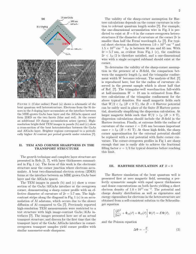
Figure 1: (Color online) Panel (a) shows a schematic of thebent quantum well heterostructure. Electrons from the Si do-nors in the δ-doping layer accumulate at the interface betweenthe MBE-grown GaAs base layer and the AlGaAs spacer andform 2DES on the two facets (blue and red). At the corneran additional 1D charge accumulation arises (green). High-resolution bright-field TEM images in panels (b) and (c) showa cross-section of the bent heterointerface between the GaAsand AlGaAs layer. Brighter regions correspond to a periodi-cally higher Al content per period growth under rotation [7].
II. TEM AND CORNER SHARPNESS IN THETRANSPORT STRUCTURE
The growth technique and complete layer structure arepresented in Refs. [1, 7], with layer thicknesses summari-zed in Fig. 1 (a). The focus of this work is the electronicstructure near the corner junction where electrons accu-mulate. A bent two-dimensional electron system (2DES)forms at the interface between an MBE grown GaAs baselayer and the AlGaAs spacer.
The TEM images in panels (b) and (c) show a cross-section of the GaAs/AlGaAs interface at the overgrowncorner, demonstrating a sharp corner profile with an ef-fective diameter of curvature of 2r = 5.7 nm. The high-contrast stripe along the diagonal in Fig. 1 (c) is an accu-mulation of Al adatoms, which occurs due to the slowerdiffusion of Al compared to Ga [7]. Previously reportedhigh-resolution TEM measurements were restricted to atest structure with high image-contrast GaAs/AlAs in-terfaces [7]. The images presented here are of an actualtransport structure, and discern for the first time that thetransport layer of the GaAs/AlGaAs interface in corner-overgrown transport samples yield corner profiles withsimilar nanometer-scale sharpness.
The validity of the sharp-corner assumption for Har-tree calculations depends on the corner curvature in rela-tion to relevant quantum length scales [7]. For example,the one-dimensional accumulation wire in Fig. 3 is pre-dicted to exist at B = 0 in the corner-overgrown hetero-structures if the diameter of curvature at the corner 2r issmaller than half the Fermi wavelength λF [7]. For typi-cal sheet electron densities between 1.0× 1011 cm−2 and1.5 × 1011 cm−2 λF is between 80 nm and 65 nm. With2r = 5.7 nm, as evident from Fig. 1 (c), the condition2r < λF /2 is therefore satisfied, and a one-dimensionalwire with a single occupied subband should exist at thecorner.
To determine the validity of the sharp-corner assump-tion in the presence of a B-field, the comparison bet-ween the magnetic length lB and the triangular confine-ment width W becomes relevant. The analysis of Ref. [7]is reproduced here, but for the radius of curvature ob-served in the present sample which is about half thatof Ref. [7]. The triangular-well wavefunction full-widthat half-maximum W = 18 nm is estimated from Har-tree calculations of the triangular confinement for theabove typical densities. For small magnetic fields suchthat W/2 < lB (B < 8 T), the B = 0 Hartree potentialcan be safely used in place of the finite B Hartree poten-tial, drastically simplifying the dispersion calculation. Atlarger magnetic fields such that W/2 > lB (B > 8 T),dispersion calculations should include the B-field in theHartree iteration. Finally, at extreme fields the radius ofcurvature of the corner r = 2.85 nm becomes importantonce r > lB (B > 81 T). At these high fields, the sharpcorner approximation for the external potential shouldbe replaced with a real potential with finite corner cur-vature. The corner-overgrown profiles in Fig 1 are sharpenough that one is easily able to achieve the fractionalfilling factor ν = 1/3 for typical densities before reachingthis limit.
III. HARTREE SIMULATION AT B = 0
The Hartree simulation of the bent quantum well ispresented first at zero magnetic field, assuming a per-fectly symmetric sample with equal spacer thicknessesand donor concentrations on both facets yielding a sheetelectron density of 1.0× 1011 cm−2. The potential andcharge density distribution as well as eigenstates andenergy eigenvalues for electrons in the heterostructure areobtained from a self-consistent solution to the Schroedin-ger equation[
(~p)2
2m?+ Φcb(~r) + Φel(~r)
]Ψ(~r) = EΨ(~r), (1)
and the Poisson equation
∆Φ = −%ε. (2)

3
Figure 2: Self-consistent B = 0 Hartree potential Φfor the bent quantum well heterostructure, plotted alonga perpendicular cross-section through one of the facets.The two-dimensional electron densities on both facets are1× 1011 cm−2. The inset figure shows that the diagonal cross-section through the corner has almost exactly twice the confi-nement potential as the perpendicular cross-section far fromthe corner. A 1D accumulation wire results from the additio-nal depth of the potential at the corner.
where ~r = (x, y, z) is the position vector, % is thecharge density, and ε is the low-frequency dielectricconstant for AlGaAs or GaAs, respectively. The poten-tial Φcb is defined by the conduction band of the intrinsicGaAs/AlGaAs semiconductor crystal as well as ionizeddopants, and Φel is the Hartree potential of the electrondistribution solved for overall charge neutrality. In thefollowing the total potential Φ = Φcb + Φel will be re-ferred to as the Hartree potential. The Poisson equationis solved for a finite cross-section of the heterostructurewith the boundary conditions
Φsurf = 0,
~Esub = 0,
where the conduction band potential Φsurf at the samplesurface and the electric field ~Esub at the interface to thebulk of the sample are set to zero. This surface potentialassumes mid-gap pinning of the cap layer.
The Hartree potential Φ obtained from the self-consistent solution to Eqs. (1) and (2) is plotted in Fig. 2along a perpendicular cross-section through one facet farfrom the corner as a function of the distance d fromthe sample surface. The conduction band bending at theGaAs/AlGaAs interface defines an approximately trian-gular quantum well which hosts the 2DES in the facets.The inset shows the potential ΦS (z′) (ΦS (x′)), along aperpendicular cross-section through the left (right) fa-cet far from the corner (solid line), and the potential Φc
along a diagonal cross-section through the corner junc-
Figure 3: (Color online) Panel (a) shows the two coordinateframes defined for the Hartree simulations at finite B. The(xc, y, z)-frame is used for the ky-momentum and xc-cyclotronorbit center coordinates, with the z-axis parallel to ~B. The(x′, z′) coordinate frame fixed to the sample is convenient toplot the electronic wavefunctions in real-space. The plots inpanel (b) show the calculated electron densities projected ontothe x-axis indicated in the schematic, where the blue and redcurves are the 2D electron densities in the facets and theblue and red lines at the bottom represent eigenenergies ofstates in the facets. The green curve is the density of the1D accumulation wire with eigenenergy represented by thegreen line at the bottom of the figure. The black curve showsthe total electron density. Panel (c) displays the calculatedbinding energies for the 2D and 1D states.
tion (dotted line). Due to the confinement in both x′- andz′-direction the corner potential Φc has about twice thebinding potential compared to the facets. The additionaldepth of the potential well at the corner causes the 1Daccumulation with a binding energy of 7 meV, comparedto 3.5 meV for electrons in the 2D facets.
Fig. 3 (b) shows the electron density calculated atB = 0, integrated over the quantum well thickness andprojected onto the xc-axis indicated in panel (a). We dis-tinguish three different electron systems in the cornerregion : The 2D systems in the facets plotted in red orblue, respectively, and a 1D accumulation wire plottedin green. Panel (c) shows the calculated binding energiesrelative to the Fermi level EF for 2D and 1D states in thebent quantum well, where the 1D wire is approximatelytwice as deeply bound as the 2D ground energies, due todouble confinement in z′-and x′-directions. Note that thediscrete spectrum of 2D states is an artifact of the finitesize of the quantum mechanical simulation.

4
Figure 4: (Color online) (a) Hartree dispersions E vs. cyclo-tron orbit center xc (momentum ky) corresponding to the wa-vefunctions |ψ0
⟩, |ψ1
⟩, |ψ2
⟩(black) of the bent quantum Hall
system. Magnetic field is 1.5 T at a tilt angle θ = 45◦. The sixFermi points responsible for conduction are labelled a throughf and are discussed further in Figs. 5 and 6. The anticrossingat xc = 0 has its bonding and anti-bonding states labelled gand h, respectively, and is discussed further in Fig. 7. (b) Thesubsystems model of an idealized sharp QH edge. Dispersionsfor the left-facet |Ln
⟩(blue) and right-facet |Rn
⟩(red) sub-
systems, and the parabolic dispersion of the 1D wire groundstate |W0
⟩(green) subsystem are shown. The dotted lines and
shaded areas indicate the effective orbit center position of thecorner walls as seen by the edge states. For easy comparisonof the Hartree solution to the subsystems model, each solu-tions is plotted in half-tone in the background of the otherplot. Wavefunctions for each dispersion branch are labelledaccording to the discussion in Section IV.
IV. HARTREE SIMULATION AT FINITE B
Having identified the 2D and 1D states that exist in abent quantum well at zero magnetic field, we now studythe new states that emerge from these subsystems at fi-nite B. If a tilted magnetic field is applied such that the2D electron systems of both facets are in a quantum Hallstate, all three subsystems are strongly coupled and formthe bent quantum Hall system. In this paper we restrictourselves to BQH systems where the magnetic field is ap-plied at a 45◦-angle such that the 2D systems on bothfacets are in the same quantum Hall state with filling fac-tor ν. Zeeman spin splitting and exchange interactionsare neglected.
It has been previously shown that the electron scree-ning charge density at zero B serves as an excellent ap-proximation to the charge density at finite B [8]. Anysmall deviations in charge distribution come only fromthe possible existence of dipolar strips at the boundarybetween compressible and incompressible strips whichare themselves a consequence of screening of Landau-quantized electron density of states in a slowly varyingedge potential. Edge tunneling experiments by Huber, etal. [9] have shown that abrupt quantum Hall boundarieswith sharp potentials have vanishingly small incompres-sible strips. Thus the zero B Hartree potential will beassumed to serve as an excellent approximation to thefinite B Hartree potential. The presence of a magneticfield will simply add harmonic cyclotron-motion to thetotal Hamiltonian, derived for completeness below.
It is convenient to pick a coordinate frame (x, y, z),where the z-axis is defined by the magnetic field and they-axis is the translationally invariant direction along thecorner of the bent quantum well, as shown in Fig. 3 (a).We choose the vector potential ~A in the Landau gauge topreserve y-translational invariance and make momentumky a good quantum number :
~A = xBy, (3)
which satisfies the condition
~B = ~∇× ~A = Bz (4)
As an Ansatz for the wavefunctions, we choose
Ψ(~r) = ψn,ky (x, z)eikyy (5)
or identically
Ψ(~r) = ψn,xc(x, z)eixcy/l
2B (6)
where the cyclotron orbit center xc is proportional toy-momentum xc = kyl
2B where lB =
√~eB is the ma-
gnetic length, and n is the energy eigenvalue index. Onlythe lowest electrostatically confined sub-band is occupiedin these heterostructures, so n represents the hybridizedLandau subband / wire subband index. With the an-

5
satz (6) the explicitly y-dependent parts can be separatedfrom the Schroedinger equation[
(~p− e ~A)2
2m?+ Φ(x, z)
]Ψ(~r) = EΨ(~r), (7)
and one obtains[(p2x + p2z)
2m?+
1
2m?ω2
c (x− xc)2 + Φ(x, z)
]ψn,xc
(x, z)
= En(xc)ψn,xc(x, z). (8)
We see that the magnetic field causes the additional har-monic potential 1
2m?ω2
c (x − xc)2 in the x-direction per-pendicular to ~B, where ωc = eB
m? is the cyclotron fre-quency.
Fig. 4 (a) shows the dispersion calculated for a bentquantum well with sheet electron densities n = 1.0 ×1011 cm−2 in both facets, where a magnetic field of 1.5 Tapplied at a tilt angle θ = 45◦ relative to the facet nor-mal vectors brings both 2D systems to the ν = 4 quantumHall state. The dispersion of this bent quantum Hall sys-tem is plotted in black as energy E versus the momentumky (top axis) and the orbit center xc (bottom axis).
V. SUBSYSTEMS MODEL
To provide intuition as to the origin of these states,we define three separate subsystems which hybridize toform the bent quantum well system, namely the left facetquantum well, the right facet quantum well, and the 1Daccumulation wire at the corner. All subsystems are 1Din character, as their energy is uniquely determined interms of a single spatial coordinate, the cyclotron orbitcenter xc. We will show that not only the overall disper-sion, but also the wavefunctions themselves can be quan-titatively predicted from such a subsystems model. Thecandidate wavefunctions at a given orbit center coordi-nate are generated by taking the subsystem wavefunctionat the desired orbit center and energy and projecting outall more deeply bound states at the same orbit center toform an orthogonal basis.
A. Subsystem dispersions
The separate left-facet and right-facet quantum wellsubsystems are modeled as heterojunction triangular-wellpotentials which terminate abruptly in a 0.3 eV hard wallat the corner, defined in Fig. 3(a) as a wall at x′0 for theleft facet and at z′0 for the right facet. Note that thehard wall boundary perceived by a given quantum wellarises because of the sudden 90◦ bend in the heterojunc-tion. The result is a pair of coupled orthogonally facinghard-wall-like QH edge dispersions. When projected ontoa common axis, such as x, the finite width of the wa-
vefunction results in different projected positions of theeffective hard wall for the opposing dispersions.
The triangular well potential is taken to be the Hartreesolution of the quantum well far from the junction ΦS ascalculated in Section III.
ΦL(x′, z′) =
{ΦB , x′ < x′0ΦS(z′) , x′ > x′0
(9)
ΦR(x′, z′) =
{ΦB , z′ < z′0ΦS(x′) , z′ > z′0
(10)
and ΦB = EF + 0.3 eV is used to approximate the cornerheterojunction barrier.
The confinement potential ΦW (x′, z′) of the 1D accu-mulation wire is modeled as the sum of two orthogonaltriangular potentials
ΦW (x′, z′) = ΦS(x′) + ΦS(z′). (11)
In analogy to Eq. (8) for the Hartree simulation, theleft, right, and wire subsystems satisfy the followingSchroedinger equations :[
(p2x + p2z)
2m?+
1
2m?ω2
c (x− xc)2 + ΦL
]Ln,xc
(x, z)
= ELn (xc)Ln,xc(x, z) (12)
[(p2x + p2z)
2m?+
1
2m?ω2
c (x− xc)2 + ΦR
]Rn,xc
(x, z)
= ERn (xc)Rn,xc(x, z) (13)
[(p2x + p2z)
2m?+
1
2m?ω2
c (x− xc)2 + ΦW
]Wn,xc
(x, z)
= EWn (xc)Wn,xc(x, z) (14)
The dispersion calculated for the left-facet quantumwell is shown in blue in Fig. 4 (b), mirrored by the reddispersion of the right-facet quantum well at B = 1.5 T,ν = 4. Effective positions for the hard wall seen by ei-ther facet is indicated by vertical dotted lines, offset fromthe geometric center by the projected finite width of thewavefunction. The deeply bound accumulation wire is in-dicated by the green parabolic dispersion in Fig. 3.
The dispersions of these constituent systems inFig. 4(b) clearly represent the key features of the to-tal Hartree dispersion shown in Fig. 4(a). First, the low-energy dispersion of the 1D subsystem accumulation wireperfectly matches the dispersion of the full Hartree cal-culation at low energies. The quantum Hall edge subsys-tems also parallel the branches of the full Hartree calcu-lation, though the energies of the subsystem edge statesare slightly lower. This may be a result of level repulsionwhich is not taken into account in the subsystems model.
Coupling between the different subsystems arises be-

6
cause of interpenetration of the wavefunctions at the cor-ner. Semiclassically, one can consider an electron at lowmagnetic fields spending most of its time executing thearc of its cyclotron orbit within the facet, but for a shorttime perturbed by states at the corner as it reflects spe-cularly from the hard wall. Quantum mechanically, theinterpenetration of the counter-propagating edge statesfrom the two orthogonal facets and the accumulation wireat the corner, gives rise to anticrossing gaps at all inter-sections of the subsystem dispersions. States with lar-ger spatial overlap integral (such as the wire and facetstates) have larger coupling and larger anticrossing gaps,whereas states with less spatial overlap (such as betweenopposing facets) have smaller anticrossing gaps. The to-tal dispersion of the bent quantum Hall system emergesas a hybrid system of these three coupled 1D subsystemdispersions along the corner.
The states which are responsible for determining elec-tron conduction along the corner are those where thedispersion curves cross the Fermi level EF , highlightedin Fig. 4 (a) and labelled a through f . The direction ofpropagation of each mode is determined by the slope ofthe dispersion at EF , where a positive slope leads to aforward-propagating mode and a negative slope yieldsa reverse-propagating mode. The left-facet edge statesb and d (blue) as well as the wire state f are forward-propagating, and the right-facet edge states c and e (red)and wire state a are reverse-propagating. At low magne-tic fields and integer filling factor such that the facetsare gapped, such as ν = 4 in Fig. 4 (a), the Hartree simu-lations show ν spin-degenerate conducting modes fromeach quantum Hall edge. The 1D accumulation wire addstwo spin-degenerate modes in each direction and servesas an additional 1D channel for scattering. Together withthe 1D edge modes from the QH systems, the model thuspredicts up to N = ν + 2 one-dimensional modes in eachdirection.
Fig. 5 shows the real-space wavefunctions of these same1D modes a through f from Fig. 4 (a). The sharp edgepotential allows for a finite overlap of the wavefunc-tions, so that any disorder potential can scatter chargebetween dispersion branches, including backscattering.Overlap integrals between different backscattering statesat EF are calculated, ranging from the smallest over-lap
⟨b|e⟩
= 0.027, to a typical value⟨c|d⟩
= 0.076,to the largest overlap integral for backscattering states⟨a|f⟩
= 0.420 which is found inside the wire. One the-refore does not expect to observe universal conductancevalues for the corner conductance, but instead to measurenon-universal values which characterize scattering alongsuch a corner [2].
B. Subsystem wavefunctions
In this section we show how the wavefunctions of thetotal hybrid system can be understood in terms of the wa-vefunctions of the individual subsystem eigenstates. We
Figure 5: (Color online) Color-map plots of the probabilitydensities for real-space wavefunctions corresponding to thevarious 1D modes marked in Fig. 4 (a). The electrons in thefacets (blue and red) and corner accumulation wire (green)are colored according to their Hartree dispersions shown inFig. 4 (b).
Figure 6: (Color online) (a) Crossections along the z′-axis atx′ = 0 of the right quantum Hall edge subsystem wavefunc-tions |R0
⟩, |R1
⟩and the 1D accumulation wire subsystem
|W0
⟩at B = 1.5 T and xc = 22 nm. (b) Candidate wavefunc-
tions |θ1⟩and |θ2
⟩for the combined bent quantum well system
are constructed by projecting out the deeply bound wire state|W0
⟩from the QH edge subsystem according to Eqs. 17 and
19. Together with the wire ground state these states show ex-cellent agreement with the Hartree eigenstates |ψ0
⟩, |ψ1
⟩, and
|ψ2
⟩at xc = 22 nm obtained from the numerical simulation
of the complete bent quantum Hall system (inset equations),confirming the correspondence with the subsystems model.
begin by examining states away from the anticrossings,and will define trial states |θn
⟩in terms of the subsys-
tem states |Ln
⟩, |Rn
⟩, and |Wn
⟩, all with the same or-
bit center xc. The explicit functional dependence on theorbit center xc will be dropped hereafter, since all wa-vefunctions must have the same xc value to constituteky-momentum eigenstates.
To start, consider an orbit center 0 < xc < 40 nmwhere the wire has the lowest ground state energy. Wi-thin this range, the state |W0
⟩at the bottom of Fig. 6(a)
is a good trial for the proper Hartree ground state |ψ0
⟩,
leading us to the ground state ansatz |θ0⟩.
|θ0⟩
= |W0
⟩(15)
The case for xc = 22 nm is plotted in the bottom of

7
Fig. 6(b). The overlap between this trial state and theHartree solution shows excellent agreement :
⟨ψ0|θ0
⟩= 0.999 (16)
The next higher subsystem state at this xc is |R0
⟩shown in the middle of Fig. 6(a). This state is not or-thogonal to the ground state |θ0
⟩, so the trial state for
our first excited energy |θ1⟩requires that we project out
this ground state :
|θ1⟩
= N1
{|R0
⟩− |θ0
⟩⟨θ0|R0
⟩}(17)
where N1 is a normalization constant. The resulting wa-vefunction is shown in the middle of Fig. 6(b) and over-laps very well with the Hartree solution |ψ1
⟩⟨ψ1|θ1
⟩= 0.978 (18)
Continuing to the next higher energy wavefunction, thestate |R1
⟩shown at the top of Fig. 6(a) needs to be made
orthogonal to all states |θ1⟩and |θ0
⟩below it, thereby
generating the trial state |θ2⟩:
|θ2⟩
= N2
{|R1
⟩− |θ0
⟩⟨θ0|R1
⟩−|θ1
⟩⟨θ1|R1
⟩}(19)
Again the result strongly overlaps with the Hartree solu-tion |ψ2
⟩⟨ψ2|θ2
⟩= 0.915 (20)
In general, if one defines the energetically ordered se-quence of subsystem states at a given xc called |Sn
⟩,
which for this example was |S0
⟩= |W0
⟩, |S1
⟩= |R0
⟩,
|S2
⟩= |R1
⟩..., then trial wavefunctions can be generated
from the expression below :
|θn⟩
= Nn
{1−
∑i=0...n−1
|θi⟩⟨θi|
}|Sn
⟩(21)
These trial states confirm that the low energy Hartreeeigenstates for the total corner quantum well can be un-derstood in terms of the subsystem wavefunctions.
Finally, we examine the wavefunctions at an anticros-sing such as xc = 0 to check how the above expressionfor trial states changes in the case of degeneracy. Foranticrossing states in Fig. 4(a) designated as points gand h, the subsystem states |L0
⟩and |R0
⟩are degene-
rate, so the sequence of states |Sn
⟩needs to be modified
to consider first the symmetric, and then the antisym-metric combination : |S0
⟩= |W0
⟩, |S1
⟩= |R0
⟩+ |L0
⟩,
|S2
⟩= |R1
⟩− |L0
⟩. Fig. 7 shows color map plots of the
wavefunctions ψn(x′, z′) corresponding to states at thexc = 0 anti-crossing of the left and right quantum Halledges. The states |θL
⟩and |θR
⟩are constructed from the
wavefunctions |L0
⟩and |R0
⟩separately, whereas |θ1
⟩and
|θ2⟩take the degeneracy into account, and show excellent
agreement (97-98% overlap) with the Hartree results |ψ1
⟩and |ψ2
⟩for the binding or anti-binding states at the
xc = 0 anti-crossing gap.
VI. HARTREE SIMULATION AT LARGE B
Fig. 8 shows Hartree dispersions of the bent QH sys-tem at various magnetic fields. With increasing B theanti-crossing gaps in the dispersion increase, indicatingan increasing coupling among the three constituent sub-systems. This follows from the reduced magnetic length,which brings all quantum confined 1D states closer to thecorner, and therefore in stronger overlap with each other.This is in contrast to planar barrier systems, for examplethe planar antiwire of Refs. [10, 11], where the couplingdecreases exponentially at high B. The strong anticros-sings result in both positive curvatures, corresponding toan electron-like mass, and negative curvatures, represen-ting a hole-like mass, in various parts of the dispersion.The band gaps between hybridized Landau bands startto become larger than the band-widths of the higher exci-ted bands. The signature feature of a bound wire state atthe corner evolves at high magnetic fields into a centraldispersion minimum for the lowest band.
VII. INTERPRETATION OF EXPERIMENTS
A series of transport experiments have already beenperformed on bent quantum Hall systems. Conduc-tance measurements along the BQH junction have shownweakly insulating, strongly insulating and metallic beha-vior, depending on ν [2]. At low magnetic fields (ν =3, 4, 5, 6) weakly insulating behavior was observed, witha finite, yet non-universal conductance of a few percentof the quantized value νe2/h and little temperature- ordc voltage bias dependence. In contrast, the conductanceat higher magnetic fields (ν = 1, 2) showed strongly insu-lating behavior and decreased drastically with decreasingtemperature or voltage. Finally, at the fractional fillingfactor ν = 1/3 the BQH junction showed metallic beha-vior, where the conductance strongly increased upon lo-wering the temperature or voltage. Possible explanationsfor the unique transport properties of the bent quantumHall junction, can be sought within the microscopic mo-del presented here.
We discuss first the experimental case of integer fillingfactor ν ≥ 3, which was observed to be a weak insula-tor [2, 3]. The microscopic model for such a system wasshown here to be a 1D multimode conductor such as in

8
Figure 7: (Color online) Candidate wavefunctions for anticrossing points g and h in the dispersion of Fig. 4 are shown ascolor scale probability amplitudes. Energy degenerate trial states |θL
⟩and |θR
⟩are plotted, along with their symmetric and
antisymmetric combinations |θ1⟩and |θ2
⟩, respectively. The resulting wavefunctions agree very well with the numerical Hartree
results |ψ1
⟩for point g and |ψ2
⟩for point h, with an overlap integral of 97% - 98%.
Figure 8: Hartree dispersions of a bent quantum Hall junc-tion at various magnetic fields. In contrast to planar barriersystems where the gaps vanish exponentially at high B, herethe anti-crossing gaps due to strong coupling of the modes atthe corner increase with increasing magnetic field.
Fig. 4(a) for the ν = 4 dispersion case, with Fermi pointsfor each mode indexed i = a...f . Note that the expe-riments of Huber et al. [9] have demonstrated that ata sharp edge potential, the wavefunctions of different co-propagating edge states are close enough to each other tospatially overlap. In Fig. 6 we see a similar scenario, but
in addition, the counter-propagating states also overlap.A disorder potential V (x′, y, z′) thus allows backscatte-ring of charge among these Fermi points in Fig. 4(a) .
To understand how to notate momentum scattering inthe bent QH system, the Fourier transform of the disor-der potential can be taken in the y direction along thelength of the corner :
Vky(x′, z′) =
∫dy e−ikyy V (x′, y, z′) (22)
Using the notation of Eq. 6 for the wavefunction, the di-sorder scattering matrix element between Fermi points iand j can be expressed as :
Vij =⟨ψni,xi
(x′, z′)|Vkij(x′, z′) |ψnj ,xj
(x′, z′)⟩
(23)
where ni and xi are the energy subband index and cy-clotron orbit center of the ith Fermi point, and kij =(xj − xi)/l2B is the momentum scattering wavevector interms of the orbit center coordinates. The expression canthus be used to describe the experimentally observednon-universal conductance for ν ≥ 3 in terms of disorder-induced scattering among various 1D modes.
Next we discuss the experimental case of integer fillingfactor ν = 1, 2, which was observed to be strongly insula-ting. A detailed analysis of the experimental temperatureand voltage dependence has already been performed, andreveals 1D hopping conduction along the corner, with 1Dactivated hopping at higher temperatures (T > 320 mK)giving way to 1D variable range hopping at low tempe-

9
ratures (T < 320 mK) [2, 3]. We can understand thisin terms of the Hartree simulations calculated here inthe high-B limit, such as in Fig. 8 which shows a bandinsulator at large B. Although band conduction is inhi-bited since none of the dispersions intersect the Fermienergy, the conventional understanding of the QHE ack-nowledges that disorder will induce localized states wi-thin the gap. When the Fermi energy sits within theselocalized states, standard theory of semiconductors [14]would predict activated hopping conduction among lo-calized states at higher temperatures, which would giveway to variable range hopping within the impurity bandat lower temperatures, as seen experimentally. The intri-guing observation is that hopping conduction appears totake place only along the 1D corner junction whereas it issuppressed in the facets. This could be caused by an en-hanced the density of disorder localized states at the cor-ner, which results from dips in the hybridized dispersionsat the corner (see bottom-right panel of Fig. 8). Thus theHartree calculations are able to provide a plausible mi-croscopic model for the strongly insulating behavior atν = 1, 2.
Finally we discuss the experimental case of extrememagnetic fields of approximately 23 T needed to reachν = 1/3 in both facets [2]. A proper electrostatic mo-deling of this case would require a self-consistent treat-ment including electron-electron interactions to correctlyarrive at the Laughlin ground state in the facets, andconduction of charge along the corner would have to bedescribed in terms of 1/3-charge quasiparticles. Thus anymodel proposed here will be speculative in nature. No-netheless, even though such numerical calculations arebeyond the scope of this work, one can still arrive at aqualitative picture by considering the electrostatics re-vealed by the single particle picture in the high fieldlimit. Fig. 8 identifies the energy minimum due to theaccumulation wire at the center of the corner to be seve-ral mV below the ground energy in the facets. Whereasthe ground state far from the corner is expected to bea standard Laughlin state with probability of occupancy1/3 per state, the deep energetic minimum at the cornerwill exceed the interaction gap energy and thus be fullyoccupied with one electron per state. The corner thusrepresents a ν = 1/3 : 1 : 1/3 junction.
As discussed in Refs. [2, 5, 6], coupled fractional QHedges can result in the 1D metallic behavior in the so-called anti-wire geometry. In this system, two counter-propagating ν = 1/3 edges backscatter electron chargethrough a depeted ν = 0 vacuum. it is important thatelectrons (not fractional quasiparticles) backscatter thecharge between the counter-propagating ν = 1/3 edges,so that backscattering of charge becomes less and lessrelevant at decreasing temperatures, thus wire conducti-vity increases as the temperature drops. Prerequisites forthe anti-wire model therefore include a sufficiently strongspatial overlap of counter-propagating edge modes to al-low charge scattering, and an effective ’vacuum’ for thefractional quasiparticles between edge modes to ensure
that electrons, not fractional quasiparticles, are backscat-tered. The Hartree simulations presented in this paper in-fer that both conditions are fulfilled in the bent quantumHall system at hand. The dispersions shown in Fig. 8 indi-cate an increasing coupling of counter-propagating edgestates leading to spatial overlap of the wavefunctions, andthe 1D accumulation wire in Fig. 4 can function as an ef-fective vacuum for the ν = 1/3 quasiparticles, since atν = 1 no fractional excitations can exist in the fully oc-cupied deeply bound wire-region of the dispersion. Thusthe Hartree simulations allow us to construct a candidatepicture of the high B field metallic behavior at the cornerjunction in terms of a quantum Hall anti-wire.
This situation is in contrast to the scenario of the pla-nar anti-wire geometry originally proposed in Refs. [2, 5,6] and implemented in Refs. [10, 11]. Here the tunnel bar-rier separating the two coplanar QH systems exponen-tially suppresses tunneling at high B, thereby prohibi-ting the desired strong coupling of fractional QH edges.We thus propose that, at the high magnetic fields neces-sary to see ν = 1/3 edges, the bent quantum Hall systemmay actually be the only experimentally realizable sys-tem which can show the predicted ’anti-wire’ system ofRefs. [5, 6], because the corner geometry allows the strongcoupling of two distinct ν = 1/3 edges.
VIII. CONCLUSION
We have studied a new type of low-dimensional sys-tem, the bent quantum Hall junction, in spin-degenerateHartree simulations, providing an elementary understan-ding of the various coupled electronic states existing insuch a non-planar junction of two quantum Hall sys-tems. We have shown how the electronic dispersion andeigenstates in this hybrid system can still be quantita-tively understood in terms of the dispersion and eigens-tates of constituent QW facet and accumulation wire sub-systems. Such analysis can simplify future simulations :instead of a fully numerical solution to the Schroedin-ger equation one could solve the 1D Hartree potentialof a single quantum well, and then construct the dis-persion and eigenstates from template wavefunctions ofthe subsystem states. With such a semi-analytical ap-proach the simulations could also be extended to allowfor self-consistent simulations at finite magnetic fields orto approximate the hybridized fractional QH states ex-pected in the BQH junction at high B. The simulationsclearly demonstrate how the bent quantum Hall systemdiffers from any tunnel-coupled planar system of counter-propagating QH edges. Particularly the increasing wa-vefunction overlap of the edge states with increasing Bmakes it an interesting device to study coupled fractionalquantum Hall edges, and possibly the only system wherethe predicted 1D metallic behavior at ν = 1/3 can beobserved experimentally.

10
Acknowledgments
This work was supported by the Deutsche Forschungs-gemeinschaft in the Schwerpunktprogramm QuantenHall Systeme, by DFG GR 2618/1-1, by NSF CAREERAward DMR-0748856, the Sonderforschungsbereich SFB621 and the Nanosystems Initiative Munich.†corresponding author : [email protected]

11
[1] M. Grayson, D. Schuh, M. Huber, M. Bichler and G. Abs-treiter, Appl. Phys. Lett. 86, 032101 (2005) ; D. Schuh,M. Grayson, M. Bichler and G. Abstreiter, Physica E 23,293 (2004).
[2] M. Grayson, L. Steinke, D. Schuh, M. Bichler, L. Hoep-pel, J. Smet, K. v. Klitzing, D. K. Maude and G. Abstrei-ter, Phys. Rev. B 76, 201304(R) (2007) ; L. Steinke, D.Schuh, M. Bichler, G. Abstreiter and M. Grayson, Phys.Rev. B 77, 235319 (2008).
[3] L. Steinke, Ph. D. Thesis, Technische Universität Mün-chen (2009).
[4] M. Grayson, D. Schuh, M. Bichler, M. Huber, G. Abs-treiter, L. Hoeppel, J. Smet, K. von Klitzing, Physica E22, 181 (2004).
[5] C. L. Kane and M. P. A. Fisher, Phys. Rev. B 46, 15233(1992).
[6] S. R. Renn and D. P. Arovas, Phys. Rev. B 51, 16832(1995).
[7] L. Steinke, P. Cantwell, D. Zakharov, E. Stach, N. J. Za-
luzec, A. Fontcuberta i Morral, M. Bichler, G. Abstrei-ter and M. Grayson, Applied Physics Letters 93, 193117(2008).
[8] D. B. Chklovskii, B. I. Shklovskii, and L. I. Glazman,Phys. Rev. B 46, 4026(1992).
[9] M. Huber, M. Grayson, M. Rother, W. Biberacher, W.Wegscheider and G. Abstreiter, Phys. Rev. Lett. 94,016805 (2005).
[10] W. Kang, H. L. Stormer, L. N. Pfeiffer, K. W. Baldwinand K. W. West, Nature 403, 59 (2000).
[11] M. Habl, M. Reinwald, W. Wegscheider, M. Bichler andG. Abstreiter, Phys. Rev. B 73, 205305 (2006).
[12] X. G. Wen, Phys. Rev. Lett. 64, 2206 (1990).[13] M. Grayson, D. C. Tsui, L. N. Pfeiffer, K. W. West and
A. M. Chang, Phys. Rev. Lett. 86, 2645 (2001).[14] B. I. Shklovskii and A. L. Efros, Electronic Properties
of Doped Semiconductors, (Springer series in solid statesciences ; 45), Chapter 8-9, Berlin Heidelberg (1984).
Copyright © 2022 FDOKUMEN