Growth of NiO ultrathin films on Pd(1 0 0) by post-oxidation of Ni films: the effect of pre-adsorbed...
19
Growth of NiO ultrathin films on Pd(1 0 0) by post-oxidation of Ni films: the effect of pre-adsorbed oxygen M. Sambi * , R. Sensolo, G.A. Rizzi, M. Petukhov 1 , G. Granozzi Unit a di Ricerca INFM and Dipartimento di Chimica Inorganica, Metallorganica e Analitica, Universit a di Padova, Via Loredan 4, 35131 Padova, Italy Received 27 February 2003; accepted for publication 2 May 2003 Abstract This paper reports on the optimisation of the growth parameters of NiO ultrathin films on Pd(1 0 0). Growth is performed by means of UHV metal deposition and post-oxidation cycles. Chemical and structural characterisation of the deposits is achieved by means of electron spectroscopy (X-ray photoelectron spectroscopy, XPS; angle resolved XPS) and electron diffraction techniques (low energy electron diffraction, LEED; X-ray photoelectron diffraction, XPD). Three growth procedures have been investigated, which differ for the particular growth parameters adopted in each case. We demonstrate that post-oxidation is effective in order to obtain epitaxial NiO only if the initial dose of Ni evaporated on the clean Pd(1 0 0) substrate exceeds a critical value, corresponding approximately to two equivalent monolayers. However, the overlayer thus obtained is strongly understoichiometric in oxygen close to the metal/oxide interface and poorly ordered on the long range. When a Ni dose below this limiting first value is used, the layer evolves toward polycrystalline NiO, due to substantial oxidation of the Pd substrate promoted by the presence of Ni, very likely through a work function decrease upon direct metal/metal interface formation. On the contrary, epitaxial NiO(1 0 0) layers of good structural quality, with limited oxygen deficiency at the interface, with negligible substrate oxidation and with a good degree of long-range order are obtained if deposition and post-oxidation cycles are initiated on an oxygen pre-saturated Pd surface, characterised by the ( p 5 p 5)-R27° O/Pd(1 0 0) LEED pattern. We therefore demonstrate that oxygen can act either as an inhibitor or as a promoter of NiO epitaxial growth on Pd(1 0 0), depending on the way it is used. Ó 2003 Elsevier Science B.V. All rights reserved. Keywords: Nickel oxides; Oxidation; Palladium; Epitaxy; X-ray photoelectron spectroscopy; Low energy electron diffraction (LEED); Growth 1. Introduction MgO and NiO ultrathin films grown on Ag(1 0 0) are by now well-established model sys- tems in which a simple and a strongly correlated oxide, respectively, having analogous rocksalt lattice structures and similar lattice parameters are * Corresponding author. Tel.: +39-049-827-5189; fax: +39- 049-827-5161. E-mail address: [email protected] (M. Sambi). 1 Present address: IGNP, Russian Research Center, Kur- chatov Institute, Kurchatov sq., 123182 Moscow, Russia. 0039-6028/03/$ - see front matter Ó 2003 Elsevier Science B.V. All rights reserved. doi:10.1016/S0039-6028(03)00641-1 Surface Science 537 (2003) 36–54 www.elsevier.com/locate/susc
-
Upload
transumanisti -
Category
Documents
-
view
0 -
download
0
Transcript of Growth of NiO ultrathin films on Pd(1 0 0) by post-oxidation of Ni films: the effect of pre-adsorbed...
Surface Science 537 (2003) 36–54
www.elsevier.com/locate/susc
Growth of NiO ultrathin films on Pd(1 0 0) bypost-oxidation of Ni films: the effect of pre-adsorbed oxygen
M. Sambi *, R. Sensolo, G.A. Rizzi, M. Petukhov 1, G. Granozzi
Unit�aa di Ricerca INFM and Dipartimento di Chimica Inorganica, Metallorganica e Analitica, Universit�aa di Padova,
Via Loredan 4, 35131 Padova, Italy
Received 27 February 2003; accepted for publication 2 May 2003
Abstract
This paper reports on the optimisation of the growth parameters of NiO ultrathin films on Pd(1 0 0). Growth is
performed by means of UHV metal deposition and post-oxidation cycles. Chemical and structural characterisation of
the deposits is achieved by means of electron spectroscopy (X-ray photoelectron spectroscopy, XPS; angle resolved
XPS) and electron diffraction techniques (low energy electron diffraction, LEED; X-ray photoelectron diffraction,
XPD).
Three growth procedures have been investigated, which differ for the particular growth parameters adopted in each
case. We demonstrate that post-oxidation is effective in order to obtain epitaxial NiO only if the initial dose of Ni
evaporated on the clean Pd(1 0 0) substrate exceeds a critical value, corresponding approximately to two equivalent
monolayers. However, the overlayer thus obtained is strongly understoichiometric in oxygen close to the metal/oxide
interface and poorly ordered on the long range. When a Ni dose below this limiting first value is used, the layer evolves
toward polycrystalline NiO, due to substantial oxidation of the Pd substrate promoted by the presence of Ni, very likely
through a work function decrease upon direct metal/metal interface formation. On the contrary, epitaxial NiO(1 0 0)
layers of good structural quality, with limited oxygen deficiency at the interface, with negligible substrate oxidation and
with a good degree of long-range order are obtained if deposition and post-oxidation cycles are initiated on an oxygen
pre-saturated Pd surface, characterised by the (p5�p
5)-R27� O/Pd(1 0 0) LEED pattern. We therefore demonstrate
that oxygen can act either as an inhibitor or as a promoter of NiO epitaxial growth on Pd(1 0 0), depending on the way
it is used.
� 2003 Elsevier Science B.V. All rights reserved.
Keywords: Nickel oxides; Oxidation; Palladium; Epitaxy; X-ray photoelectron spectroscopy; Low energy electron diffraction (LEED);
Growth
* Corresponding author. Tel.: +39-049-827-5189; fax: +39-
049-827-5161.
E-mail address: [email protected] (M. Sambi).1 Present address: IGNP, Russian Research Center, Kur-
chatov Institute, Kurchatov sq., 123182 Moscow, Russia.
0039-6028/03/$ - see front matter � 2003 Elsevier Science B.V. All r
doi:10.1016/S0039-6028(03)00641-1
1. Introduction
MgO and NiO ultrathin films grown on
Ag(1 0 0) are by now well-established model sys-
tems in which a simple and a strongly correlated
oxide, respectively, having analogous rocksalt
lattice structures and similar lattice parameters are
ights reserved.
M. Sambi et al. / Surface Science 537 (2003) 36–54 37
matched epitaxially to a fcc transition metal
characterised by a valence band of predominantly
5sp character close to the Fermi level [1]. Epitaxy
is favoured by the low lattice mismatch between
the overlayers and the metal for this particular
substrate choice. A rich debate has been under-taken in the literature in order to elucidate the
modifications of the oxides� structural and elec-
tronic properties and of their chemical reactivity
due to the presence of the strong compositional
gradient introduced by the overlayer/metal inter-
face. In this context, the importance of the image
charge potential induced by the ionic cores of the
overlayer in the substrate in evaluating the ener-getics of the interface has been stressed [2,3].
In this work, Pd(1 0 0) has been tested as an
alternative metal substrate for NiO epitaxy. Al-
though it is less appealing from the point of view
of the lattice mismatch, which is significantly lar-
ger than for silver (+7.3% vs +2.2%, respectively),
nonetheless it gives the opportunity of investigat-
ing the interfacial interactions between the oxideand a metal with a valence band of predominantly
4d character near the Fermi level. This is helpful
in order to assess the role and importance of
the hybridisation of overlayer and metal states at
the interface in determining the properties and the
reactivity of the system, also by comparison with
the qualitatively different Ag case. The NiO/
Pd(1 0 0) interface is also interesting from the pointof view of magnetic properties. Although peculiar
magnetisation properties have been demonstrated
for NiO/Pd superlattices (which show ferromag-
netic behaviour, while bulk Pd and NiO are
paramagnetic and antiferromagnetic, respectively)
[4,5], interestingly enough, no surface science in-
vestigation has been performed up to now to elu-
cidate in detail the structure of the NiO/Pdinterface.
For all these reasons, the first issue to be ad-
dressed is the establishment of a growth procedure
which leads reproducibly to epitaxial NiO ultra-
thin films of good quality on Pd(1 0 0).
Oxide layers are usually grown either via reac-
tive deposition (RD, i.e. metal evaporation in the
presence of oxygen or of another oxidising agent,e.g. NO2 [6]) or, less frequently, via post-oxidation
(PO) of small amounts of metal deposited on the
substrate in UHV conditions [7]. In the present
paper, we explore the PO route, which consists in
depositing small amounts of Ni on the clean sub-
strate at RT, followed by PO in oxygen at 450 K.
Results concerning the RD procedure will be the
argument of a forthcoming paper.Here we show that, when Pd(1 0 0) is used as the
substrate, the microstructure and the composition
of the overlayer are strongly dependent on the
deposition procedure. Both properties are essen-
tially driven by the surface chemistry of the sub-
strate itself towards oxygen (which shows a rather
complex phase diagram for oxygen adsorption)
and by the competition between Pd and Nitowards oxidation during the first stages of PO
deposition. In fact, four distinct oxygen chemi-
sorption phases on Pd(1 0 0) are known as a
function of coverage [8], ranging from p(2 · 2)
through c(2 · 2) and (5 · 5) to the saturation phase
(p5�p
5)-R27� (indicated for brevity as ‘‘p5
structure’’ in the following), while a complete ox-
idation of subsurface Pd layers is not attainablestarting from clean palladium in high vacuum
conditions (oxygen pressures up to 10�5 mbar).
However, this picture is substantially modified by
the presence of Ni, which––as will be shown––
promotes Pd oxidation in certain conditions, with
direct consequences on the quality of the epitaxial
overlayer.
By combining X-ray photoelectron spectro-scopy (XPS), angle resolved XPS (ARXPS) [9], an-
gle scanned X-ray photoelectron diffraction (XPD)
[10] and low energy electron diffraction (LEED)
measurements, in this work we explore such a
complex behaviour. Its understanding allows us to
set up a deposition procedure which leads to a
sharp interface between epitaxial and homoge-
neous NiO ultrathin films and metallic Pd(1 0 0).
2. Experimental
Sample treatments were performed in an UHV
preparation chamber at a base pressure of 5 · 10�11
mbar. The Pd(1 0 0) crystal was cleaned by re-
peated cycles of argon ion sputtering (KE¼ 2.4keV), and annealing at T ¼ 970 K with a final
flash in 1 · 10�6 mbar O2 (uncorrected ion gauge
38 M. Sambi et al. / Surface Science 537 (2003) 36–54
reading). The exposure to oxygen ensured the re-
moval of the carbon contaminant segregating to
the surface during each annealing cycle, and left
the surface free from either C or O, as judged by
grazing angle XPS measurements. The cleaning
cycles were repeated until a sharp (1 · 1) LEED(VG Microtech Rear View LEED––RVL900)
pattern was observed and a good anisotropy de-
veloped in Pd 3d XPD scans.
NiO layers were grown with Ni metal deposi-
tion and PO cycles. Three different growth proce-
dures were followed, characterised by different Ni
doses at each cycle and/or by substrate pre-satu-
ration with oxygen. Common features to all pro-cedures were the following: Ni depositions were
performed at room temperature (RT) by means of
an electron beam evaporator (Caburn MDC,
model EB90). PO treatments were performed by
dosing 60 L of O2 at RT, followed by 150 L with
the substrate held at T ¼ 440 K. The oxygen dose
at RT was performed in order to initiate the
overlayer oxidation while avoiding as muchas possible Ni diffusion into the substrate. The
deposition rate of NiO resulting from such treat-
ments was estimated to be �2.15� 0.10 �AA/min, as
determined by XPS calibrations (see below).
Thickness values expressed in ML equivalents
(MLeq) are calculated assuming an interlayer dis-
tance between adjacent planes in NiO(1 0 0) equal
to 2.09 �AA. When oxygen pre-saturation of thesubstrate has been exploited, it has been per-
formed by dosing 600 L of O2 at T ¼ 570 K,
resulting in a (p5�p
5)-R27� O/Pd(1 0 0) LEED
pattern, as reported in the literature [11].
XPS and XPD data were collected using a
modified VG ESCALAB MKII photoelectron
spectrometer. The sample was mounted on a two-
axis goniometer which allowed the sweeping of theelectron emission direction with an angular reso-
lution of �1� both in polar angle (h, defined with
respect to the surface normal) and in azimuthal
angle (/, defined with respect to the [0 1 1] direc-
tion on the surface). The acceptance half-angle of
the electron analyser was estimated to be 3.5�.ARXPS measurements were performed in order
to obtain an estimate of the growth rate andgrowth mode of the overlayer [9]. Intensities as a
function of the polar angle h were obtained for Pd
3d (BE� 335 eV for the 3d5=2 component) and Ni
2p (BE� 854 eV for the 2p3=2 component) photo-
electron signals.
XPD scans for structural analysis were obtained
for Pd 3d emission from the clean substrate and
for Ni 2p3=2 photoelectron and O KLL Augeremission from NiO ultrathin films as a function of
overlayer thickness. Line intensities are reported
after a simple linear background subtraction.
Unmonochromatised Al Ka radiation was used in
the experiment, except where explicitly stated.
3. Results and discussion
3.1. Deposition procedure I: polycrystalline NiO
layers
The first deposition procedure explored in the
present work consisted in 1 min of Ni deposition,
followed by PO, as specified above in the experi-
mental section. Metal deposition and PO cycleshave been repeated for a total deposition time of
14 min.
3.1.1. ARXPS data
ARXPS has been used to estimate the growth
rate and the growth mode resulting from the
adopted procedure. Fig. 1 reports the ratio between
the background-subtracted overlayer Ni 2p andsubstrate Pd 3d integral XPS peak intensities as a
function of the sine of the acquisition angle vs the
sample surface. The experimental data for different
deposition times (dots) are fitted with the standard
ARXPS equation for patched overlayer growth [9]
(lines). Data have been acquired after each minute
of deposition up to 6 min, and after each 2 min
thereafter. The ratio K between Ni 2p and Pd 3dintensities from, respectively, NiO and Pd samples
of semi-infinite thickness and inelastic attenuation
lengths for the overlayer and the substrate photo-
electrons in the NiO matrix (6.7 and 16 �AA, respec-
tively, calculated by means of the TPP-2 formula
[12] for Al Ka-excited emission) are used as input
data. The covered surface fraction c and the aver-
age islands thickness z are the fitting output.c and z as a function of deposition time are
reported in Fig. 2a. The error bars represent one
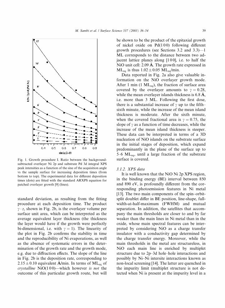
Fig. 1. Growth procedure I. Ratio between the background-
subtracted overlayer Ni 2p and substrate Pd 3d integral XPS
peak intensities as a function of the sine of the acquisition angle
vs the sample surface for increasing deposition times (from
bottom to top). The experimental data for different deposition
times (dots) are fitted with the standard ARXPS equation for
patched overlayer growth [9] (lines).
M. Sambi et al. / Surface Science 537 (2003) 36–54 39
standard deviation, as resulting from the fitting
procedure at each deposition time. The product
c � z, shown in Fig. 2b, is the overlayer volume per
surface unit area, which can be interpreted as the
average equivalent layer thickness (the thicknessthe layer would have if the growth were perfectly
bi-dimensional, i.e. with c ¼ 1). The linearity of
the plot in Fig. 2b confirms the stability in time
and the reproducibility of Ni evaporations, as well
as the absence of systematic errors in the deter-
mination of the growth rate and the growth mode,
e.g. due to diffraction effects. The slope of the line
in Fig. 2b is the deposition rate, corresponding to2.15� 0.10 equivalent �AA/min. In terms of MLeq of
crystalline NiO(1 0 0)––which however is not the
outcome of this particular growth route, but will
be shown to be the product of the epitaxial growth
of nickel oxide on Pd(1 0 0) following different
growth procedures (see Sections 3.2 and 3.3)––1
ML corresponds to the distance between two ad-
jacent lattice planes along [1 0 0], i.e. to half the
NiO unit cell: 2.09 �AA. The growth rate expressed inMLeq is thus 1.02� 0.05 MLeq/min.
Data reported in Fig. 2a also give valuable in-
formation on the NiO overlayer growth mode.
After 1 min (1 MLeq), the fraction of surface area
covered by the overlayer amounts to c ¼ 0:28,while the mean overlayer islands thickness is 6.8 �AA,
i.e. more than 3 ML. Following the first dose,
there is a substantial increase of c up to the fifth–sixth minute, while the increase of the mean island
thickness is moderate. After the sixth minute,
when the covered fractional area is c ¼ 0:75, the
slope of c as a function of time decreases, while the
increase of the mean island thickness is steeper.
These data can be interpreted in terms of a 3D
nucleation of NiO islands on the substrate surface
in the initial stages of deposition, which expandpredominantly in the plane of the surface up to
5–6 MLeq, until a large fraction of the substrate
surface is covered.
3.1.2. XPS data
It is well known that the NiO Ni 2p XPS region,
in the binding energy (BE) interval between 850
and 890 eV, is profoundly different from the cor-responding photoemission features in Ni metal
[13]. The two main components of the spin–orbit-
split doublet differ in BE position, line-shape, full-
width-at-half-maximum (FWHM) and mutual
separation. In addition, the satellites that accom-
pany the main thresholds are closer to and by far
weaker than the main lines in Ni metal than in the
oxide, whose main spectral features can be inter-preted by considering NiO as a charge transfer
insulator with a conductivity gap determined by
the charge transfer energy. Moreover, while the
main thresholds in the metal are structureless, in
NiO each main line is enriched by multiplet
structure due to 2p–3d hole–hole interactions and
possibly by Ni–Ni intersite interactions known as
non-local screening [14]. The latter are quenched inthe impurity limit (multiplet structure is not de-
tected when Ni is present at the impurity level in a
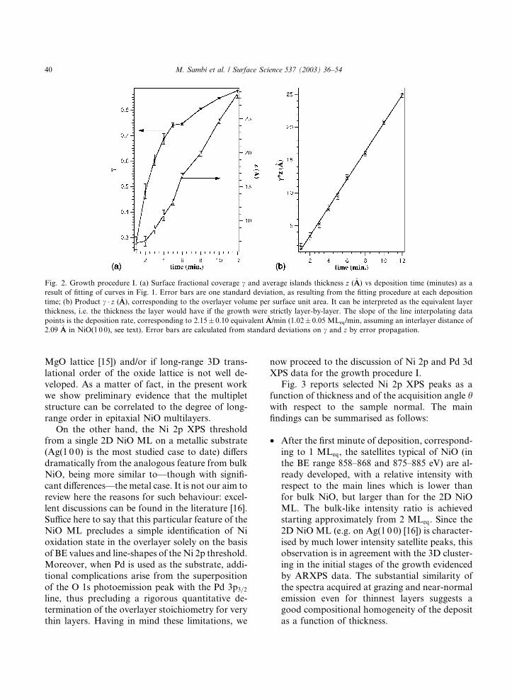
Fig. 2. Growth procedure I. (a) Surface fractional coverage c and average islands thickness z (�AA) vs deposition time (minutes) as a
result of fitting of curves in Fig. 1. Error bars are one standard deviation, as resulting from the fitting procedure at each deposition
time; (b) Product c � z (�AA), corresponding to the overlayer volume per surface unit area. It can be interpreted as the equivalent layer
thickness, i.e. the thickness the layer would have if the growth were strictly layer-by-layer. The slope of the line interpolating data
points is the deposition rate, corresponding to 2.15� 0.10 equivalent �AA/min (1.02� 0.05 MLeq/min, assuming an interlayer distance of
2.09 �AA in NiO(1 0 0), see text). Error bars are calculated from standard deviations on c and z by error propagation.
40 M. Sambi et al. / Surface Science 537 (2003) 36–54
MgO lattice [15]) and/or if long-range 3D trans-
lational order of the oxide lattice is not well de-
veloped. As a matter of fact, in the present work
we show preliminary evidence that the multiplet
structure can be correlated to the degree of long-
range order in epitaxial NiO multilayers.On the other hand, the Ni 2p XPS threshold
from a single 2D NiO ML on a metallic substrate
(Ag(1 0 0) is the most studied case to date) differs
dramatically from the analogous feature from bulk
NiO, being more similar to––though with signifi-
cant differences––the metal case. It is not our aim to
review here the reasons for such behaviour: excel-
lent discussions can be found in the literature [16].Suffice here to say that this particular feature of the
NiO ML precludes a simple identification of Ni
oxidation state in the overlayer solely on the basis
of BE values and line-shapes of the Ni 2p threshold.
Moreover, when Pd is used as the substrate, addi-
tional complications arise from the superposition
of the O 1s photoemission peak with the Pd 3p3=2
line, thus precluding a rigorous quantitative de-termination of the overlayer stoichiometry for very
thin layers. Having in mind these limitations, we
now proceed to the discussion of Ni 2p and Pd 3d
XPS data for the growth procedure I.
Fig. 3 reports selected Ni 2p XPS peaks as a
function of thickness and of the acquisition angle hwith respect to the sample normal. The main
findings can be summarised as follows:
• After the first minute of deposition, correspond-
ing to 1 MLeq, the satellites typical of NiO (in
the BE range 858–868 and 875–885 eV) are al-
ready developed, with a relative intensity with
respect to the main lines which is lower than
for bulk NiO, but larger than for the 2D NiO
ML. The bulk-like intensity ratio is achievedstarting approximately from 2 MLeq. Since the
2D NiO ML (e.g. on Ag(1 0 0) [16]) is character-
ised by much lower intensity satellite peaks, this
observation is in agreement with the 3D cluster-
ing in the initial stages of the growth evidenced
by ARXPS data. The substantial similarity of
the spectra acquired at grazing and near-normal
emission even for thinnest layers suggests agood compositional homogeneity of the deposit
as a function of thickness.
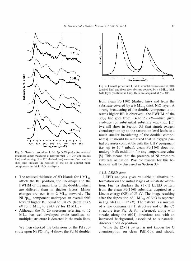
Fig. 3. Growth procedure I. Ni 2p XPS peaks for selected
thickness values measured at near-normal (h ¼ 24�, continuousline) and grazing (h ¼ 72�, dashed line) emission. Vertical da-
shed lines indicate the position of the Ni 2p doublet main
components in thick NiO overlayers.
Fig. 4. Growth procedure I. Pd 3d doublet from clean Pd(1 0 0)
(dashed line) and from the substrate covered by a 6 MLeq thick
NiO layer (continuous line). Data are acquired at h ¼ 60�.
M. Sambi et al. / Surface Science 537 (2003) 36–54 41
• The reduced thickness of 3D islands for 1 MLeq
affects the BE position, the line-shape and the
FWHM of the main lines of the doublet, which
are different than in thicker layers. Minor
changes are seen from 2 MLeq onwards. The
Ni 2p3=2 component undergoes an overall shift
toward higher BE equal to 0.8 eV (from 853.6
eV for 1 MLeq to 854.4 eV for 12 MLeq).• Although the Ni 2p spectrum referring to 12
MLeq has well-developed oxide satellites, no
multiplet structure is detected in the main lines.
We then checked the behaviour of the Pd sub-
strate upon Ni PO. Fig. 4 shows the Pd 3d doublet
from clean Pd(1 0 0) (dashed line) and from the
substrate covered by a 6 MLeq thick NiO layer. A
strong broadening of the doublet components to-
wards higher BE is observed––the FWHM of the
3d5=2 line goes from 1.4 to 2.2 eV––which gives
evidence for substantial substrate oxidation [17](we will show in Section 3.3 that simple oxygen
chemisorption up to the saturation level leads to a
much smaller broadening of the doublet compo-
nents). It should be remarked that in oxygen par-
tial pressures compatible with the UHV equipment
(i.e. up to 10�5 mbar), clean Pd(1 0 0) does not
undergo bulk oxidation for any temperature value
[8]. This means that the presence of Ni promotessubstrate oxidation. Possible reasons for this be-
haviour will be discussed in Section 3.4.
3.1.3. LEED data
LEED analysis gives valuable qualitative in-
formation on the initial stages of substrate oxida-
tion. Fig. 5a displays the (1 · 1) LEED pattern
from the clean Pd(1 0 0) substrate, acquired at akinetic energy (KE) of 55 eV. The image resulting
after the deposition of 1 MLeq of NiO is reported
in Fig. 5b (KE¼ 57 eV). The pattern is a mixture
of a two domains (2 · 1) structure and of thep5
structure (see Fig. 5c for reference), along with
streaks along the h001i directions and with an
increased background, associated to substantial
disorder upon deposition.While the (2 · 1) pattern is not known for O
chemisorption on clean Pd(1 0 0), and should
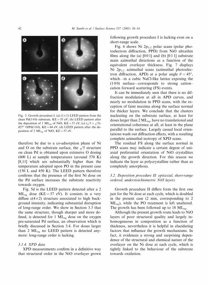
Fig. 5. Growth procedure I. (a) (1· 1) LEED pattern from the
clean Pd(1 0 0) substrate, KE¼ 55 eV; (b) LEED pattern after
the deposition of 1 MLeq of NiO, KE¼ 57 eV; (c) (p5�p
5)-
R27� O/Pd(1 0 0), KE¼ 64 eV; (d) LEED pattern after the de-
position of 2 MLeq of NiO, KE¼ 57 eV.
42 M. Sambi et al. / Surface Science 537 (2003) 36–54
therefore be due to a co-adsorption phase of Ni
and O on the substrate surface, thep5 structure
on clean Pd is obtained upon extensive O dosing
(600 L) at sample temperatures (around 570 K)
[8,11] which are substantially higher than the
temperature adopted upon PO in the present case
(150 L and 450 K). The LEED pattern thereforeconfirms that the presence of the first Ni dose on
the Pd surface increases the substrate reactivity
towards oxygen.
Fig. 5d is the LEED pattern detected after a 2
MLeq dose (KE¼ 57 eV). It consists in a very
diffuse c(4 · 2) structure associated to high back-
ground intensity, indicating substantial disruption
of long-range order. We show in Section 3.3 thatthe same structure, though sharper and more de-
fined, is detected for 1 MLeq dose on the oxygen
pre-saturated Pd surface, an observation which is
briefly discussed in Section 3.4. For doses larger
than 2 MLeq no LEED pattern is detected any-
more: long-range order is lacking.
3.1.4. XPD data
XPD measurements confirm in a definitive way
that structural order in the NiO overlayer grown
following growth procedure I is lacking even on a
short-range scale.
Fig. 6 shows Ni 2p3=2 polar scans (polar pho-
toelectron diffraction, PPD) from NiO ultrathin
films along the (a) [0 0 1] and (b) [0 1 1] substrate
main azimuthal directions as a function of theequivalent overlayer thickness. Fig. 7 displays
Ni 2p3=2 azimuthal scans (azimuthal photoelec-
tron diffraction, APD) at a polar angle h ¼ 45�,which––in a cubic NaCl-like lattice exposing the
(1 0 0) surface––corresponds to strong cation–
cation forward scattering (FS) events.
It can be immediately seen that there is no dif-
fraction modulation at all in APD curves, andnearly no modulation in PPD scans, with the ex-
ception of faint maxima along the surface normal
for thicker layers. We conclude that the clusters
nucleating on the substrate surface, at least for
doses larger than 2MLeq, have no translational and
orientational coherence at all, at least in the plane
parallel to the surface. Largely casual local orien-
tations wash out diffraction effects, with a resultingcomplete azimuthal isotropy of XPD scans.
The residual FS along the surface normal in
PPD scans may indicate a certain degree of uni-
axial preferential orientation of NiO crystallites
along the growth direction. For this reason we
indicate the layer as polycrystalline rather than as
completely amorphous.
3.2. Deposition procedure II: epitaxial, short-range
ordered, understoichiometric NiO layers
Growth procedure II differs form the first one
just for the Ni dose at each cycle, which is doubled
in the present case (2 min, corresponding to 2
MLeq), while the PO treatment is left unaltered.
The growth has been followed up to 18 MLeq.Although the present growth route leads to NiO
layers of poor structural quality and largely in-
homogeneous in composition as a function of
thickness, nevertheless it is helpful in elucidating
factors that influence the growth mechanisms. In
fact, it evidences a strong and surprising depen-
dence of the structural and chemical nature of the
overlayer on the Ni dose at each cycle, which istightly linked to the behaviour of the substrate
towards oxidation.
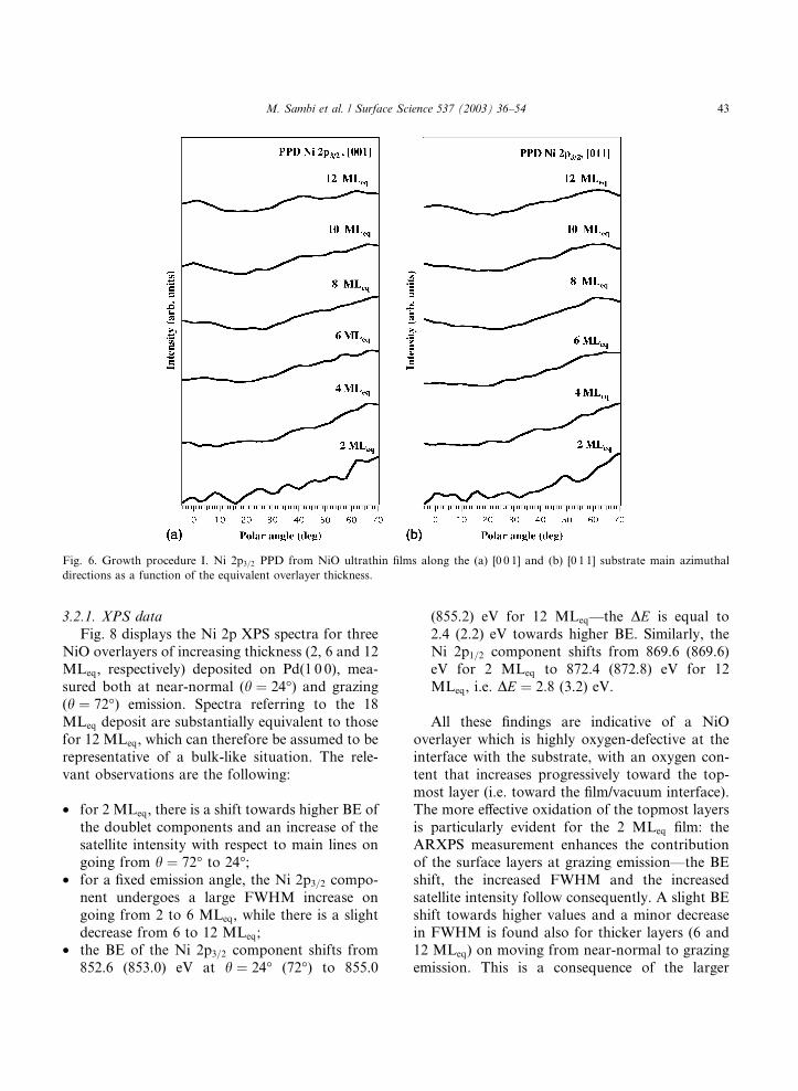
Fig. 6. Growth procedure I. Ni 2p3=2 PPD from NiO ultrathin films along the (a) [0 0 1] and (b) [0 1 1] substrate main azimuthal
directions as a function of the equivalent overlayer thickness.
M. Sambi et al. / Surface Science 537 (2003) 36–54 43
3.2.1. XPS data
Fig. 8 displays the Ni 2p XPS spectra for three
NiO overlayers of increasing thickness (2, 6 and 12MLeq, respectively) deposited on Pd(1 0 0), mea-
sured both at near-normal (h ¼ 24�) and grazing
(h ¼ 72�) emission. Spectra referring to the 18
MLeq deposit are substantially equivalent to those
for 12 MLeq, which can therefore be assumed to be
representative of a bulk-like situation. The rele-
vant observations are the following:
• for 2 MLeq, there is a shift towards higher BE of
the doublet components and an increase of the
satellite intensity with respect to main lines on
going from h ¼ 72� to 24�;• for a fixed emission angle, the Ni 2p3=2 compo-
nent undergoes a large FWHM increase on
going from 2 to 6 MLeq, while there is a slight
decrease from 6 to 12 MLeq;• the BE of the Ni 2p3=2 component shifts from
852.6 (853.0) eV at h ¼ 24� (72�) to 855.0
(855.2) eV for 12 MLeq––the DE is equal to
2.4 (2.2) eV towards higher BE. Similarly, the
Ni 2p1=2 component shifts from 869.6 (869.6)eV for 2 MLeq to 872.4 (872.8) eV for 12
MLeq, i.e. DE ¼ 2:8 (3.2) eV.
All these findings are indicative of a NiO
overlayer which is highly oxygen-defective at the
interface with the substrate, with an oxygen con-
tent that increases progressively toward the top-
most layer (i.e. toward the film/vacuum interface).The more effective oxidation of the topmost layers
is particularly evident for the 2 MLeq film: the
ARXPS measurement enhances the contribution
of the surface layers at grazing emission––the BE
shift, the increased FWHM and the increased
satellite intensity follow consequently. A slight BE
shift towards higher values and a minor decrease
in FWHM is found also for thicker layers (6 and12 MLeq) on moving from near-normal to grazing
emission. This is a consequence of the larger
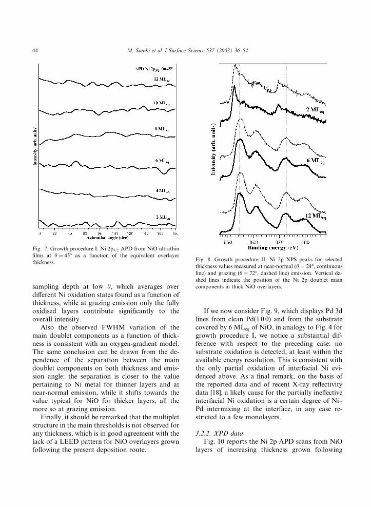
Fig. 7. Growth procedure I. Ni 2p3=2 APD from NiO ultrathin
films at h ¼ 45� as a function of the equivalent overlayer
thickness.Fig. 8. Growth procedure II. Ni 2p XPS peaks for selected
thickness values measured at near-normal (h ¼ 24�, continuousline) and grazing (h ¼ 72�, dashed line) emission. Vertical da-
shed lines indicate the position of the Ni 2p doublet main
components in thick NiO overlayers.
44 M. Sambi et al. / Surface Science 537 (2003) 36–54
sampling depth at low h, which averages over
different Ni oxidation states found as a function ofthickness, while at grazing emission only the fully
oxidised layers contribute significantly to the
overall intensity.
Also the observed FWHM variation of the
main doublet components as a function of thick-
ness is consistent with an oxygen-gradient model.
The same conclusion can be drawn from the de-
pendence of the separation between the maindoublet components on both thickness and emis-
sion angle: the separation is closer to the value
pertaining to Ni metal for thinner layers and at
near-normal emission, while it shifts towards the
value typical for NiO for thicker layers, all the
more so at grazing emission.
Finally, it should be remarked that the multiplet
structure in the main thresholds is not observed forany thickness, which is in good agreement with the
lack of a LEED pattern for NiO overlayers grown
following the present deposition route.
If we now consider Fig. 9, which displays Pd 3d
lines from clean Pd(1 0 0) and from the substrate
covered by 6 MLeq of NiO, in analogy to Fig. 4 for
growth procedure I, we notice a substantial dif-
ference with respect to the preceding case: no
substrate oxidation is detected, at least within the
available energy resolution. This is consistent withthe only partial oxidation of interfacial Ni evi-
denced above. As a final remark, on the basis of
the reported data and of recent X-ray reflectivity
data [18], a likely cause for the partially ineffective
interfacial Ni oxidation is a certain degree of Ni–
Pd intermixing at the interface, in any case re-
stricted to a few monolayers.
3.2.2. XPD data
Fig. 10 reports the Ni 2p APD scans from NiO
layers of increasing thickness grown following
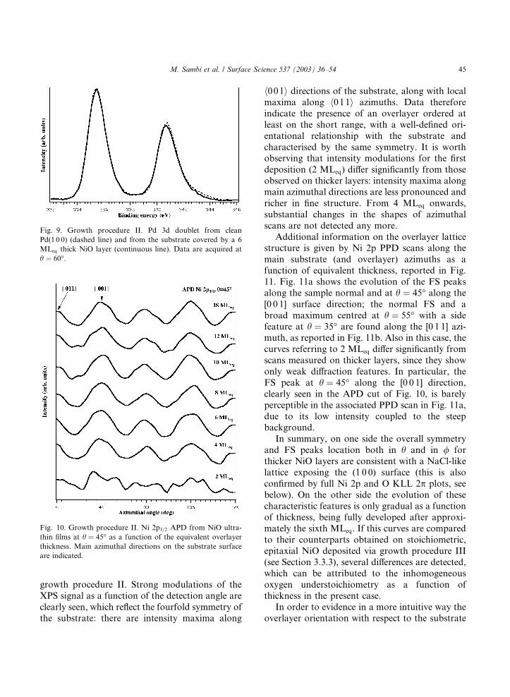
Fig. 9. Growth procedure II. Pd 3d doublet from clean
Pd(1 0 0) (dashed line) and from the substrate covered by a 6
MLeq thick NiO layer (continuous line). Data are acquired at
h ¼ 60�.
Fig. 10. Growth procedure II. Ni 2p3=2 APD from NiO ultra-
thin films at h ¼ 45� as a function of the equivalent overlayer
thickness. Main azimuthal directions on the substrate surface
are indicated.
M. Sambi et al. / Surface Science 537 (2003) 36–54 45
growth procedure II. Strong modulations of the
XPS signal as a function of the detection angle are
clearly seen, which reflect the fourfold symmetry of
the substrate: there are intensity maxima along
h001i directions of the substrate, along with local
maxima along h011i azimuths. Data therefore
indicate the presence of an overlayer ordered at
least on the short range, with a well-defined ori-
entational relationship with the substrate and
characterised by the same symmetry. It is worthobserving that intensity modulations for the first
deposition (2 MLeq) differ significantly from those
observed on thicker layers: intensity maxima along
main azimuthal directions are less pronounced and
richer in fine structure. From 4 MLeq onwards,
substantial changes in the shapes of azimuthal
scans are not detected any more.
Additional information on the overlayer latticestructure is given by Ni 2p PPD scans along the
main substrate (and overlayer) azimuths as a
function of equivalent thickness, reported in Fig.
11. Fig. 11a shows the evolution of the FS peaks
along the sample normal and at h ¼ 45� along the
[0 0 1] surface direction; the normal FS and a
broad maximum centred at h ¼ 55� with a side
feature at h ¼ 35� are found along the [0 1 1] azi-muth, as reported in Fig. 11b. Also in this case, the
curves referring to 2 MLeq differ significantly from
scans measured on thicker layers, since they show
only weak diffraction features. In particular, the
FS peak at h ¼ 45� along the [0 0 1] direction,
clearly seen in the APD cut of Fig. 10, is barely
perceptible in the associated PPD scan in Fig. 11a,
due to its low intensity coupled to the steepbackground.
In summary, on one side the overall symmetry
and FS peaks location both in h and in / for
thicker NiO layers are consistent with a NaCl-like
lattice exposing the (1 0 0) surface (this is also
confirmed by full Ni 2p and O KLL 2p plots, see
below). On the other side the evolution of these
characteristic features is only gradual as a functionof thickness, being fully developed after approxi-
mately the sixth MLeq. If this curves are compared
to their counterparts obtained on stoichiometric,
epitaxial NiO deposited via growth procedure III
(see Section 3.3.3), several differences are detected,
which can be attributed to the inhomogeneous
oxygen understoichiometry as a function of
thickness in the present case.In order to evidence in a more intuitive way the
overlayer orientation with respect to the substrate
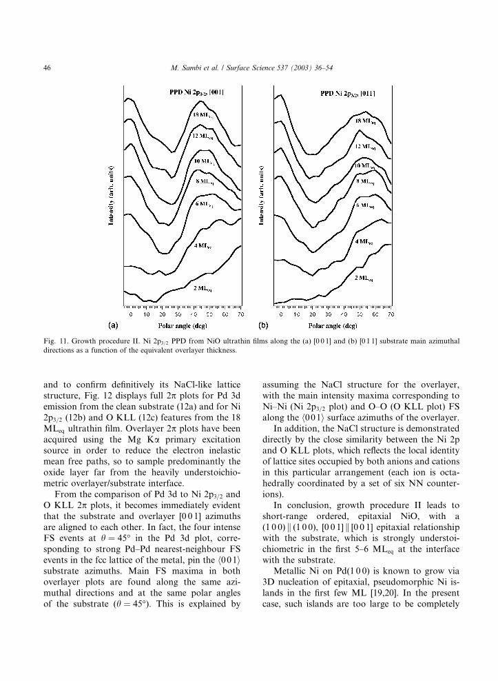
Fig. 11. Growth procedure II. Ni 2p3=2 PPD from NiO ultrathin films along the (a) [0 0 1] and (b) [0 1 1] substrate main azimuthal
directions as a function of the equivalent overlayer thickness.
46 M. Sambi et al. / Surface Science 537 (2003) 36–54
and to confirm definitively its NaCl-like lattice
structure, Fig. 12 displays full 2p plots for Pd 3d
emission from the clean substrate (12a) and for Ni
2p3=2 (12b) and O KLL (12c) features from the 18
MLeq ultrathin film. Overlayer 2p plots have been
acquired using the Mg Ka primary excitationsource in order to reduce the electron inelastic
mean free paths, so to sample predominantly the
oxide layer far from the heavily understoichio-
metric overlayer/substrate interface.
From the comparison of Pd 3d to Ni 2p3=2 and
O KLL 2p plots, it becomes immediately evident
that the substrate and overlayer [0 0 1] azimuths
are aligned to each other. In fact, the four intenseFS events at h ¼ 45� in the Pd 3d plot, corre-
sponding to strong Pd–Pd nearest-neighbour FS
events in the fcc lattice of the metal, pin the h001isubstrate azimuths. Main FS maxima in both
overlayer plots are found along the same azi-
muthal directions and at the same polar angles
of the substrate (h ¼ 45�). This is explained by
assuming the NaCl structure for the overlayer,
with the main intensity maxima corresponding to
Ni–Ni (Ni 2p3=2 plot) and O–O (O KLL plot) FS
along the h001i surface azimuths of the overlayer.
In addition, the NaCl structure is demonstrated
directly by the close similarity between the Ni 2pand O KLL plots, which reflects the local identity
of lattice sites occupied by both anions and cations
in this particular arrangement (each ion is octa-
hedrally coordinated by a set of six NN counter-
ions).
In conclusion, growth procedure II leads to
short-range ordered, epitaxial NiO, with a
(1 0 0) k (1 0 0), [0 0 1] k [0 0 1] epitaxial relationshipwith the substrate, which is strongly understoi-
chiometric in the first 5–6 MLeq at the interface
with the substrate.
Metallic Ni on Pd(1 0 0) is known to grow via
3D nucleation of epitaxial, pseudomorphic Ni is-
lands in the first few ML [19,20]. In the present
case, such islands are too large to be completely
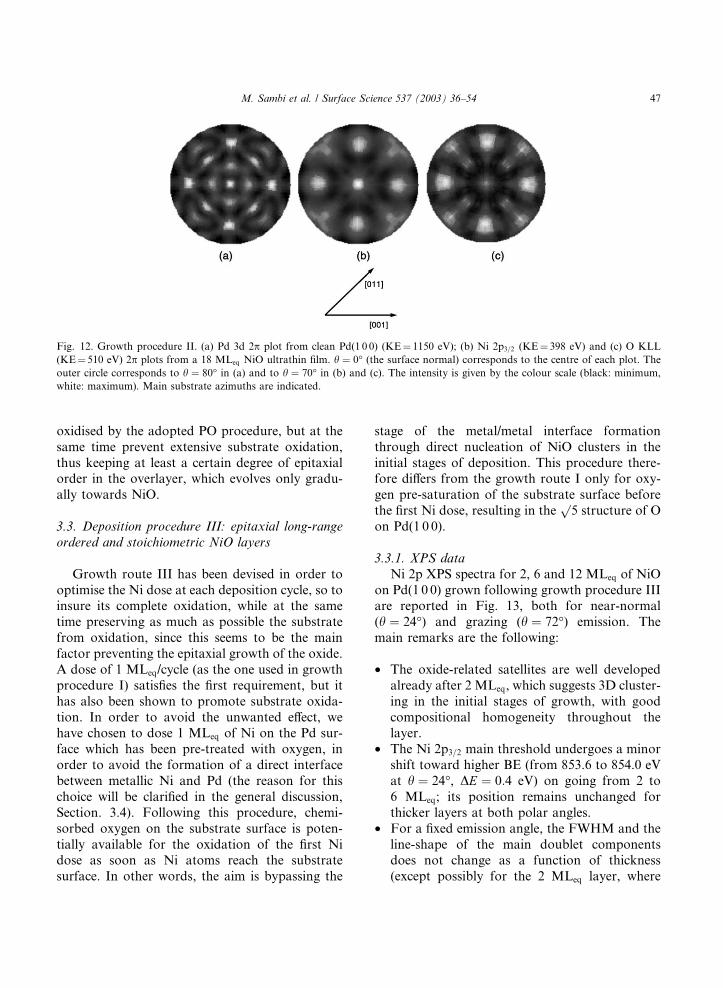
Fig. 12. Growth procedure II. (a) Pd 3d 2p plot from clean Pd(1 0 0) (KE¼ 1150 eV); (b) Ni 2p3=2 (KE¼ 398 eV) and (c) O KLL
(KE¼ 510 eV) 2p plots from a 18 MLeq NiO ultrathin film. h ¼ 0� (the surface normal) corresponds to the centre of each plot. The
outer circle corresponds to h ¼ 80� in (a) and to h ¼ 70� in (b) and (c). The intensity is given by the colour scale (black: minimum,
white: maximum). Main substrate azimuths are indicated.
M. Sambi et al. / Surface Science 537 (2003) 36–54 47
oxidised by the adopted PO procedure, but at the
same time prevent extensive substrate oxidation,
thus keeping at least a certain degree of epitaxialorder in the overlayer, which evolves only gradu-
ally towards NiO.
3.3. Deposition procedure III: epitaxial long-range
ordered and stoichiometric NiO layers
Growth route III has been devised in order to
optimise the Ni dose at each deposition cycle, so toinsure its complete oxidation, while at the same
time preserving as much as possible the substrate
from oxidation, since this seems to be the main
factor preventing the epitaxial growth of the oxide.
A dose of 1 MLeq/cycle (as the one used in growth
procedure I) satisfies the first requirement, but it
has also been shown to promote substrate oxida-
tion. In order to avoid the unwanted effect, wehave chosen to dose 1 MLeq of Ni on the Pd sur-
face which has been pre-treated with oxygen, in
order to avoid the formation of a direct interface
between metallic Ni and Pd (the reason for this
choice will be clarified in the general discussion,
Section. 3.4). Following this procedure, chemi-
sorbed oxygen on the substrate surface is poten-
tially available for the oxidation of the first Nidose as soon as Ni atoms reach the substrate
surface. In other words, the aim is bypassing the
stage of the metal/metal interface formation
through direct nucleation of NiO clusters in the
initial stages of deposition. This procedure there-fore differs from the growth route I only for oxy-
gen pre-saturation of the substrate surface before
the first Ni dose, resulting in thep5 structure of O
on Pd(1 0 0).
3.3.1. XPS data
Ni 2p XPS spectra for 2, 6 and 12 MLeq of NiO
on Pd(1 0 0) grown following growth procedure IIIare reported in Fig. 13, both for near-normal
(h ¼ 24�) and grazing (h ¼ 72�) emission. The
main remarks are the following:
• The oxide-related satellites are well developed
already after 2 MLeq, which suggests 3D cluster-
ing in the initial stages of growth, with good
compositional homogeneity throughout thelayer.
• The Ni 2p3=2 main threshold undergoes a minor
shift toward higher BE (from 853.6 to 854.0 eV
at h ¼ 24�, DE ¼ 0:4 eV) on going from 2 to
6 MLeq; its position remains unchanged for
thicker layers at both polar angles.
• For a fixed emission angle, the FWHM and the
line-shape of the main doublet componentsdoes not change as a function of thickness
(except possibly for the 2 MLeq layer, where
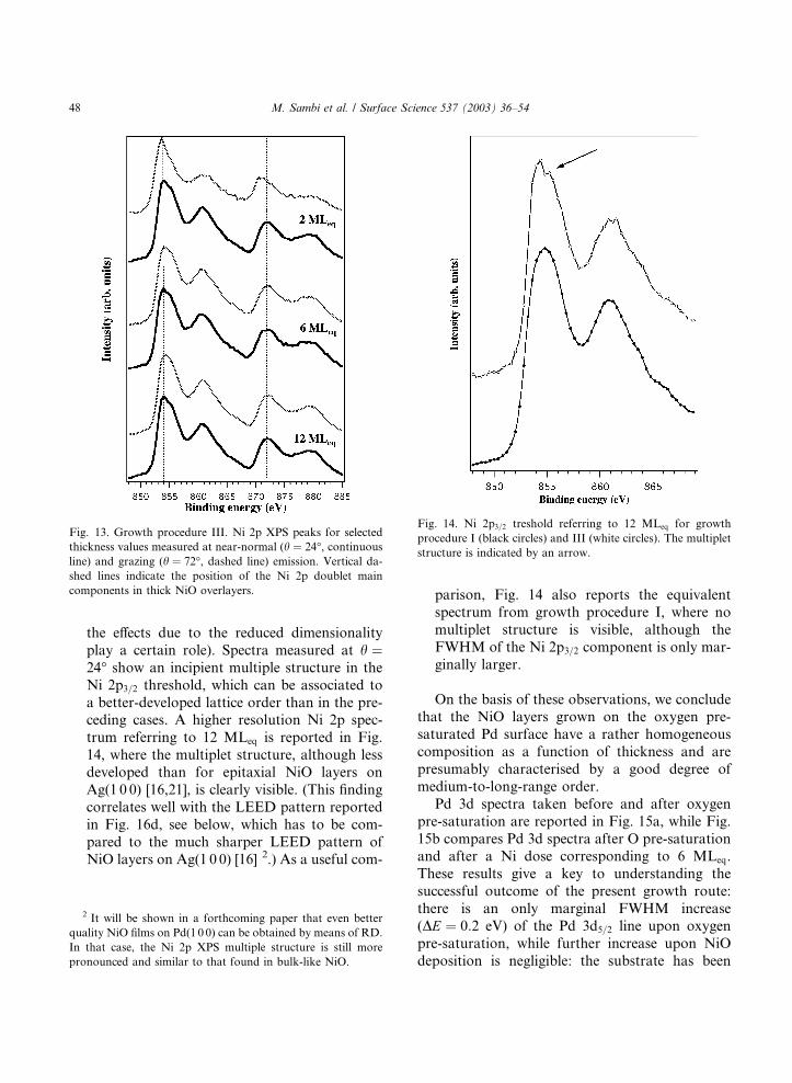
Fig. 13. Growth procedure III. Ni 2p XPS peaks for selected
thickness values measured at near-normal (h ¼ 24�, continuousline) and grazing (h ¼ 72�, dashed line) emission. Vertical da-
shed lines indicate the position of the Ni 2p doublet main
components in thick NiO overlayers.
Fig. 14. Ni 2p3=2 treshold referring to 12 MLeq for growth
procedure I (black circles) and III (white circles). The multiplet
structure is indicated by an arrow.
48 M. Sambi et al. / Surface Science 537 (2003) 36–54
the effects due to the reduced dimensionality
play a certain role). Spectra measured at h ¼24� show an incipient multiple structure in the
Ni 2p3=2 threshold, which can be associated to
a better-developed lattice order than in the pre-ceding cases. A higher resolution Ni 2p spec-
trum referring to 12 MLeq is reported in Fig.
14, where the multiplet structure, although less
developed than for epitaxial NiO layers on
Ag(1 0 0) [16,21], is clearly visible. (This finding
correlates well with the LEED pattern reported
in Fig. 16d, see below, which has to be com-
pared to the much sharper LEED pattern ofNiO layers on Ag(1 0 0) [16] 2.) As a useful com-
2 It will be shown in a forthcoming paper that even better
quality NiO films on Pd(1 0 0) can be obtained by means of RD.
In that case, the Ni 2p XPS multiple structure is still more
pronounced and similar to that found in bulk-like NiO.
parison, Fig. 14 also reports the equivalent
spectrum from growth procedure I, where no
multiplet structure is visible, although the
FWHM of the Ni 2p3=2 component is only mar-
ginally larger.
On the basis of these observations, we concludethat the NiO layers grown on the oxygen pre-
saturated Pd surface have a rather homogeneous
composition as a function of thickness and are
presumably characterised by a good degree of
medium-to-long-range order.
Pd 3d spectra taken before and after oxygen
pre-saturation are reported in Fig. 15a, while Fig.
15b compares Pd 3d spectra after O pre-saturationand after a Ni dose corresponding to 6 MLeq.
These results give a key to understanding the
successful outcome of the present growth route:
there is an only marginal FWHM increase
(DE ¼ 0:2 eV) of the Pd 3d5=2 line upon oxygen
pre-saturation, while further increase upon NiO
deposition is negligible: the substrate has been
Fig. 15. Growth procedure III. (a) Pd 3d doublet from clean
Pd(1 0 0) (dashed line) and from the substrate pre-saturated
with oxygen, giving thep5 structure (continuous line). (b) Pd
3d doublet from oxygen pre-saturated Pd(1 0 0) (dashed line)
and from the substrate covered by a 6 MLeq thick NiO layer
(continuous line). Data are acquired at h ¼ 60�.
Fig. 16. Growth procedure III. (a) LEED pattern after the first
Ni dose (1 min) on the pre-saturated Pd(1 0 0) surface and be-
fore the PO treatment, KE¼ 56 eV; (b) and (c) LEED pattern
after the first Ni dose (1 min) on the pre-saturated Pd(1 0 0)
surface and after the PO treatment, KE¼ 56 and 99 eV, re-
spectively; (d) LEED pattern of a 15 MLeq NiO film on
Pd(1 0 0), KE¼ 69 eV.
M. Sambi et al. / Surface Science 537 (2003) 36–54 49
effectively protected from extensive oxidation in
the present case.
3.3.2. LEED data
Fig. 16a shows the LEED pattern detected after
the first Ni dose (1 min) on the pre-saturated
Pd(1 0 0) surface and before the PO treatment. In-
terestingly, the image corresponds to a rather well-
defined c(4 · 2) structure, i.e. the same pattern
detected following the growth procedure I for the
second Ni dose after the PO cycle, but of betterquality. In other words, LEED suggests the for-
mation of NiO due to the reaction between the
evaporated metal and oxygen chemisorbed on the
substrate surface. The co-adsorption structure
thus formed has the same long-range symmetry
detected in the initial stages of growth following
growth procedure I. However, the lack of sub-
strate oxidation in the present case, together with
the uniform distribution of the oxidising agent on
the Pd surface (which makes it readily available for
reaction with upcoming Ni) produces a more ef-
fective long-range ordering of the overlayer. Fig.16b and c (measured at E ¼ 56 and 99 eV, re-
spectively) show the effect of the PO treatment on
the first Ni dose: the structure is still a c(4 · 2)––the
only effect of PO is a further improvement of the
long-range order in an already existing atomic
arrangement.
Finally, Fig. 16d shows the LEED pattern of a
15 MLeq NiO deposition on Pd(1 0 0) following thecurrent growth procedure. Though rather diffuse,
a (1 · 1) pattern due to NiO(1 0 0) is detected,
which was not attained with the previous growth
recipes: there is a fair degree of long-range order in
the present case.
3.3.3. XPD data
Ni 2p3=2 APD scans at h ¼ 45� from NiO filmsof increasing thickness, deposited following the
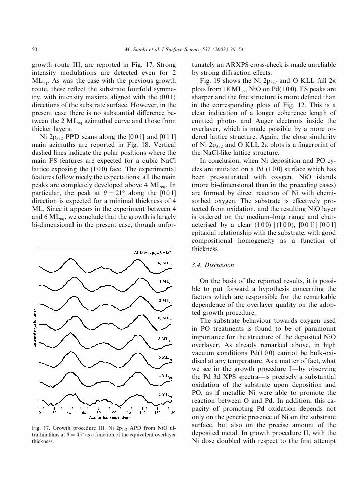
50 M. Sambi et al. / Surface Science 537 (2003) 36–54
growth route III, are reported in Fig. 17. Strong
intensity modulations are detected even for 2
MLeq. As was the case with the previous growth
route, these reflect the substrate fourfold symme-
try, with intensity maxima aligned with the h001idirections of the substrate surface. However, in thepresent case there is no substantial difference be-
tween the 2 MLeq azimuthal curve and those from
thicker layers.
Ni 2p3=2 PPD scans along the [0 0 1] and [0 1 1]
main azimuths are reported in Fig. 18. Vertical
dashed lines indicate the polar positions where the
main FS features are expected for a cubic NaCl
lattice exposing the (1 0 0) face. The experimentalfeatures follow nicely the expectations: all the main
peaks are completely developed above 4 MLeq. In
particular, the peak at h ¼ 21� along the [0 0 1]
direction is expected for a minimal thickness of 4
ML. Since it appears in the experiment between 4
and 6 MLeq, we conclude that the growth is largely
bi-dimensional in the present case, though unfor-
Fig. 17. Growth procedure III. Ni 2p3=2 APD from NiO ul-
trathin films at h ¼ 45� as a function of the equivalent overlayer
thickness.
tunately an ARXPS cross-check is made unreliable
by strong diffraction effects.
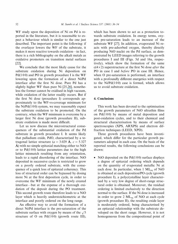
Fig. 19 shows the Ni 2p3=2 and O KLL full 2pplots from 18 MLeq NiO on Pd(1 0 0). FS peaks are
sharper and the fine structure is more defined than
in the corresponding plots of Fig. 12. This is aclear indication of a longer coherence length of
emitted photo- and Auger electrons inside the
overlayer, which is made possible by a more or-
dered lattice structure. Again, the close similarity
of Ni 2p3=2 and O KLL 2p plots is a fingerprint of
the NaCl-like lattice structure.
In conclusion, when Ni deposition and PO cy-
cles are initiated on a Pd (1 0 0) surface which hasbeen pre-saturated with oxygen, NiO islands
(more bi-dimensional than in the preceding cases)
are formed by direct reaction of Ni with chemi-
sorbed oxygen. The substrate is effectively pro-
tected from oxidation, and the resulting NiO layer
is ordered on the medium–long range and char-
acterised by a clear (1 0 0) k (1 0 0), [0 0 1] k [0 0 1]
epitaxial relationship with the substrate, with goodcompositional homogeneity as a function of
thickness.
3.4. Discussion
On the basis of the reported results, it is possi-
ble to put forward a hypothesis concerning the
factors which are responsible for the remarkabledependence of the overlayer quality on the adop-
ted growth procedure.
The substrate behaviour towards oxygen used
in PO treatments is found to be of paramount
importance for the structure of the deposited NiO
overlayer. As already remarked above, in high
vacuum conditions Pd(1 0 0) cannot be bulk-oxi-
dised at any temperature. As a matter of fact, whatwe see in the growth procedure I––by observing
the Pd 3d XPS spectra––is precisely a substantial
oxidation of the substrate upon deposition and
PO, as if metallic Ni were able to promote the
reaction between O and Pd. In addition, this ca-
pacity of promoting Pd oxidation depends not
only on the generic presence of Ni on the substrate
surface, but also on the precise amount of thedeposited metal. In growth procedure II, with the
Ni dose doubled with respect to the first attempt
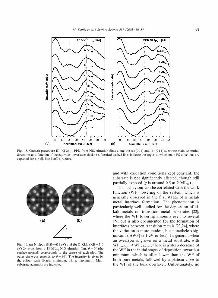
Fig. 18. Growth procedure III. Ni 2p3=2 PPD from NiO ultrathin films along the (a) [0 0 1] and (b) [0 1 1] substrate main azimuthal
directions as a function of the equivalent overlayer thickness. Vertical dashed lines indicate the angles at which main FS directions are
expected for a bulk-like NaCl structure.
Fig. 19. (a) Ni 2p3=2 (KE¼ 631 eV) and (b) O KLL (KE¼ 510
eV) 2p plots from a 18 MLeq NiO ultrathin film. h ¼ 0� (the
surface normal) corresponds to the centre of each plot. The
outer circle corresponds to h ¼ 80�. The intensity is given by
the colour scale (black: minimum, white: maximum). Main
substrate azimuths are indicated.
M. Sambi et al. / Surface Science 537 (2003) 36–54 51
and with oxidation conditions kept constant, the
substrate is not significantly affected, though still
partially exposed (c is around 0.5 at 2 MLeq).
This behaviour can be correlated with the work
function (WF) lowering of the system, which is
generally observed in the first stages of a metal/
metal interface formation. The phenomenon is
particularly well studied for the deposition of al-kali metals on transition metal substrates [22],
where the WF lowering amounts even to several
eV, but is also documented for the formation of
interfaces between transition metals [23,24], where
the variation is more modest, but nonetheless sig-
nificant (jDWFj � 1 eV or less). In general, when
an overlayer is grown on a metal substrate, with
WFoverlayer <WFsubstrate, there is a steep decrease ofthe WF in the initial stages of deposition towards a
minimum, which is often lower than the WF of
both pure metals, followed by a plateau close to
the WF of the bulk overlayer. Unfortunately, no
52 M. Sambi et al. / Surface Science 537 (2003) 36–54
WF study upon the deposition of Ni on Pd is re-
ported in the literature, but it is reasonable to ex-
pect a behaviour which is similar to the one just
described. The important point is the following: if
the overlayer lowers the WF of the substrate, it
makes it more reactive towards oxidation––in fact,there is a rich bibliography on the alkali metals as
oxidative promoters on transition metal surfaces
[22].
We conclude that the most likely cause for the
substrate oxidation during Ni deposition on
Pd(1 0 0) and PO in growth procedure I is the WF
lowering upon the formation of a direct Ni/Pd
interface after the first Ni dose. Pure Pd has aslightly higher WF than pure Ni [25,26], nonethe-
less the former cannot be oxidised in high vacuum,
while oxidation of the latter readily occurs. But if
the first Ni dose (procedure I) corresponds ap-
proximately to the WF-vs-coverage minimum for
the Ni/Pd(1 0 0) system, we may reasonably expect
the substrate oxidation to be promoted. On the
contrary, when the WF minimum is overcome by alarger first Ni dose (growth procedure II), sub-
strate oxidation is made more difficult.
Let us now discuss the microstructural conse-
quences of the substantial oxidation of the Pd
substrate in growth procedure I. It seems likely
that palladium oxide, PdO, characterised by a te-
tragonal lattice structure (a ¼ 3:029 �AA, c ¼ 5:327�AA) with no simple epitaxial matching either to NiOor to Pd(1 0 0) lattice parameters due to the high
lattice mismatch resulting from any orientation,
leads to a rapid disordering of the interface. NiO
deposited in successive cycles is restricted to grow
on a poorly ordered substrate, with the conse-
quence of a quick loss of epitaxial coherency. This
loss of structural order can be bypassed by dosing
more Ni at the first deposition cycle, in order toovercome the WF minimum of the newly created
interface––but at the expense of a thorough oxi-
dation of the deposit during the PO treatment.
This second growth route therefore leads to a NiO
layer which is heavily understoichiometric at the
interface and poorly ordered on the long range.
An effective way to avoid the formation of a
direct Ni/Pd interface is the pre-saturation of thesubstrate surface with oxygen by means of the
p5
structure of O on Pd(1 0 0) (growth route III),
which has been shown to act as a protection to-
wards substrate oxidation. In energy terms, oxy-
gen pre-saturation leads to an increase of the
substrate WF [27]. In addition, evaporated Ni re-
acts with pre-adsorbed oxygen, thereby directly
producing NiO nuclei on the Pd surface, as dem-onstrated by LEED images referring to the growth
procedures I and III (Figs. 5d and 16a, respec-
tively), which show the formation of the same
c(4 · 2) superstructure at the first Ni dose after the
PO in case I and before PO in case III. Hence,
when O pre-saturation is performed, an interface
with a profoundly different energetics with respect
to the Ni/Pd(1 0 0) case is formed, which allowsus to avoid substrate oxidation.
4. Conclusions
This work has been devoted to the optimisation
of the growth parameters of NiO ultrathin films
on Pd(1 0 0) by means of metal deposition andpost-oxidation cycles, and to their chemical and
structural characterisation by means of surface
spectroscopies (XPS, ARXPS) and electron dif-
fraction techniques (LEED, XPD).
Three growth procedures have been investi-
gated, which differ for the particular growth pa-
rameters adopted in each case. On the basis of the
reported results, the following conclusions can bedrawn:
• NiO deposited on the Pd(1 0 0) surface displays
a degree of epitaxial ordering which depends
on the quantity of evaporated metallic Ni at
each dose. In particular, when 1 MLeq of NiO
is obtained at each deposition/PO cycle (growth
procedure I), a polycrystalline layer character-ised by a very low degree of short-range struc-
tural order is obtained. Moreover, the residual
ordering is limited exclusively to the direction
normal to the surface. If the Ni dose is increased
in order to grow 2 MLeq of NiO at each cycle
(growth procedure II), the resulting oxide layer
is moderately ordered, being characterised by
an epitaxial relationship with the substrate de-veloped on the short range. However, it is not
homogeneous from the compositional point of
M. Sambi et al. / Surface Science 537 (2003) 36–54 53
view: a strong gradient of oxygen understoichi-
ometry is found at the interface with the sub-
strate.
• In growth procedure I, XPS analysis reveals a
substantial oxidation of the Pd substrate upongrowth. The reaction between oxygen and the
substrate during the PO, very likely promoted
by Ni through a WF lowering, is found to be
competitive with the nucleation of epitaxial
Ni oxide, with a resulting polycrystalline over-
layer.
• The layer obtained following growth procedure
II is characterised by a strong gradient of oxy-gen defectivity in the interfacial region, which
is reduced only starting from an overlayer thick-
ness of approximately 6MLeq. We conclude that
the first Ni dose evaporated on the Pd surface,
which is certainly epitaxial and pseudomorphic
to the substrate [19,20], prevents the substrate
oxidation (presumably both because the Ni dose
is such to imply an insufficient decrease of theWF and through direct protection). However,
it also leads to the formation of too large Ni nu-
clei, which cannot be oxidised in the adopted
PO conditions.
• In growth procedure III, the oxide deposition is
not performed directly on the clean substrate,
but on the oxygen pre-saturated Pd surface in-
stead, i.e. on the (p5�p
5)-R27� O/Pd(1 0 0)structure. The first Ni dose reacts with pre-
adsorbed oxygen (as confirmed by LEED im-
ages) so to give a NiO layer characterised by a
fair degree of long-range order, which is simply
improved by the PO treatment. In addition,
there are indications from angle resolved XPS
spectra and from XPD scans, that this route
leads to a more distinctly bi-dimensional over-layer growth. In this case, there is no occurrence
of a direct Ni/Pd interface at the Ni dose close to
the WF minimum of the system, so that the sub-
strate oxidation is largely prevented. The result
is a homogeneous NiO film, ordered in the
medium-to-long range and characterised by an
epitaxial relationship with the substrate of the
type (1 0 0) k (1 0 0), [0 0 1] k [0 0 1]. The fair de-gree of long-range order is confirmed by the
multiplet structure found in the Ni 2p3=2 thresh-
old in XPS spectra, typical of bulk NiO.
In conclusion, the most relevant feature of the
NiO/Pd(1 0 0) system highlighted by the present
work is the importance of the substrate reactivity
towards oxygen in determining the chemical na-
ture and the structural quality of the oxide over-
layer. If one succeeds in preventing substrateoxidation through the choice of the right amount
of Ni per each deposition cycle, an oxide layer
ordered at least on the short range can be ob-
tained. Finally, if the substrate is protected from
oxidation (catalysed by metallic Ni) through oxy-
gen pre-saturation and the Ni dose is sufficiently
small (so to be completely oxidised during the PO
treatment), homogeneous and medium/long-rangeordered epitaxial NiO ultrathin films are pro-
duced. Oxygen––necessary as the oxidising agent––
may act either as an inhibitor or as a promoter of
the epitaxial growth of the overlayer, depending
on the way it is used.
Many questions are left open by this work. In
particular, the intricate evolution from thep5
structure, through the c(4 · 2), ending to the (1 · 1)LEED pattern in the initial stages of deposition
should still find an explanation, a rather difficult
task if one considers that, at present, there is no
commonly accepted atomic-scale description of
the surface reconstruction leading top5 structure
of O on Pd(1 0 0). A tensor LEED analysis, per-
formed some years ago [11] and recently refined
[28], has been questioned by very recent STM datacoupled to theoretical total energy calculations
[29]. An STM study of the initial stages of growth
would therefore be helpful in giving a more precise
picture of the structural and morphological evo-
lution of the system as a function of thickness.
In addition, though many different experimen-
tal observations are nicely explained in terms of
WF variation as a function of the Ni dose, nodirect WF data for the Ni/Pd(1 0 0) system are
available––WF measurements are therefore an-
other priority.
Acknowledgements
This work has been partially funded by Minis-tero della Ricerca Scientifica e Tecnologica
(MURST) through the fund ‘‘Programmi di
54 M. Sambi et al. / Surface Science 537 (2003) 36–54
ricerca di rilevante interesse nazionale’’ and is part
of the PRA ISADORA (INFM).
References
[1] S.A. Chambers, Surf. Sci. Rep. 39 (2000) 105, and
references therein.
[2] S. Altieri, L.H. Tjeng, G.A. Sawatzky, Thin Solid Films
400 (2001) 9, and references therein.
[3] S. Altieri, L.H. Tjeng, F.C. Voogt, T. Hibma, O. Rogo-
janu, G.A. Sawatzky, Phys. Rev. B 66 (2002) 155432.
[4] T. Manago, T. Ono, H. Miyajima, K. Kawaguchi, M.
Sohma, Solid State Commun. 109 (1999) 621.
[5] T. Manago, T. Ono, H. Miyajima, I. Yamaguchi, K.
Kawaguchi, M. Sohma, Thin Solid Films 374 (2000) 21.
[6] T. Fuji, F.M.F. de Groot, G.A. Sawatzky, F.C. Voogt, T.
Hibma, K. Okada, Phys. Rev. B 59 (1999) 3195.
[7] M. Sambi, G. Sangiovanni, G. Granozzi, F. Parmigiani,
Phys. Rev. B 55 (1997) 7850.
[8] G.W. Simmons, Y.-N. Wang, J. Marcos, K. Klier, J. Phys.
Chem. 95 (1991) 4522.
[9] C.S. Fadley, Prog. Surf. Sci. 16 (1984) 275.
[10] C.S. Fadley, in: R.Z. Bachrach (Ed.), Synchrotron Radi-
ation Research: Advances in Surface Science, Plenum, New
York, 1992.
[11] D.T. Vu, K.A.R. Mitchell, O.L. Warren, P.A. Thiel, Surf.
Sci. 318 (1994) 129.
[12] S. Tanuma, C.J. Powell, D.R. Penn, Surf. Interf. Anal. 20
(1993) 77, and references therein.
[13] G.A. Sawatzky, J.W. Allen, Phys. Rev. Lett. 53 (1984)
2339.
[14] M.A. van Veenendaal, G.A. Sawatzky, Phys. Rev. Lett. 70
(1993) 2459.
[15] S. Altieri, L.H. Tjeng, A. Tanake, G.A. Sawatzky, Phys.
Rev. B 61 (2000) 13403.
[16] S. Altieri, Ph.D. Thesis, Groningen, 1999.
[17] M. Brun, A. Berthet, J.C. Bertolini, J. Electron Spectrosc.
Relat. Phenom. 104 (1999) 55.
[18] G.A. Rizzi, M. Petukhov, A. Cossaro, D. Cvetko, L.
Floreano, A. Morgante, G. Granozzi, in preparation.
[19] G.A. Rizzi, M. Petukhov, M. Sambi, G. Granozzi, Surf.
Sci. 522 (2003) 1.
[20] M. Petukhov, G.A. Rizzi, M. Sambi, G. Granozzi, Appl.
Surf. Sci. 9776 (2003) 1.
[21] P. Luches et al., Thin Solid Films 400 (2001) 139.
[22] R.D. Diehl, R. McGrath, J. Phys.: Condens. Mater. 9
(1997) 951.
[23] R.W. Vook, J.V. Bucci, S.S. Chao, Thin Solid Films 163
(1988) 447.
[24] M. Nohlen, M. Schmidt, K. Wandelt, Surf. Sci. 331–333
(1995) 902.
[25] I.D. Baikie, U. Petermann, B. L€aagel, K. Discherl, J. Vac.
Sci. Technol. A 19 (2001) 1460.
[26] Y. Fukuda, W.T. Elam, R.L. Park, Phys. Rev. B 16 (1977)
3322.
[27] J.M. Heras, G. Esti�uu, L. Viscido, Thin Solid Films 188
(1990) 165.
[28] M. Saidy, O.L. Warren, P.A. Thiel, K.A.R. Mitchell, Surf.
Sci. (2001) L799.
[29] M. Todorova et al., Surf. Sci., submitted.