Growth mechanisms of ceria- and zirconia-based epitaxial thin films and hetero-structures grown by...
9
ORIGINAL PAPER Growth mechanisms of ceria- and zirconia-based epitaxial thin films and hetero-structures grown by pulsed laser deposition Daniele Pergolesi • Marco Fronzi • Emiliana Fabbri • Antonello Tebano • Enrico Traversa Received: 28 October 2012 / Accepted: 7 December 2012 / Published online: 22 December 2012 Ó The Author(s) 2013. This article is published with open access at Springerlink.com Abstract Thin films and epitaxial hetero-structures of doped and undoped CeO 2 , and 8 mol% Y 2 O 3 stabilized ZrO 2 (YSZ), were fabricated by pulsed laser deposition on different single crystal substrates. Reflection high energy electron diffraction was used to monitor in situ the growth mechanism of the films. Two distinct growth mechanisms were identified along the (001) growth direction for the Ce- and Zr-based materials, respectively. While the doped or undoped ceria films showed a 3-dimensional growth mechanism typically characterized by a pronounced sur- face roughness, YSZ films showed an almost ideal layer- by-layer 2-dimensional growth. Moreover, when the two materials were stacked together in epitaxial hetero-struc- tures, the two different growth mechanisms were pre- served. As a result, a 2-dimensional reconstruction of the ceria-based layers determined by the YSZ film growing above was observed. The experimental results are explained in terms of the thermodynamic stability of the low-index surfaces of the two materials using computa- tional analysis performed by density functional theory. Keywords Pulsed laser deposition Á Hetero-structure Á Oxygen-ion conducting oxides Á Reflection high energy electron diffraction Á Density functional theory Introduction Thin films of doped CeO 2 and Y 2 O 3 -stabilized ZrO 2 (YSZ) fabricated by different thin film deposition methods have been widely investigated as high temperature oxygen-ion conductors. Among the most important applications of these materials is the fabrication of electrolyte membranes for solid oxide fuel cells (SOFCs). Particularly, large oxygen ion conductivity characterizes doped CeO 2 . Typi- cal dopants are Gd and Sm with concentration ranging from 10 to 20 % [1]. The bulk oxygen-ion conductivity of 15 % Sm-doped CeO 2 (SDC) is as large as 0.02 S cm -1 at about 600 °C, making this material one of the most per- forming solid state electrolyte in the so-called intermediate temperature range (500–800 °C) [2]. YSZ is also widely used as an electrolyte, for SOFCs but mostly for oxygen sensors used to control the air-to-fuel ratio in vehicles, as well as for the fabrication of thermal barrier coatings due to its low thermal conductivity [3]. Pure zirconia (ZrO 2 ) shows a complicated phase dia- gram having a monoclinic crystal structure at temperatures below about 1,000 °C, with transitions to tetragonal and cubic structures with increasing the temperature. Such phase transformations induce very large stresses that cause pure zirconia to crack, limiting its practical application. On the contrary, pure ceria (CeO 2 ) has a stable cubic phase that can easily become non-stoichiometric in oxygen con- tent, showing important catalytic activity in oxygen reduction reaction processes. This material finds many practical applications, of which the most important are in D. Pergolesi (&) Á M. Fronzi Á E. Fabbri International Research Center for Materials Nanoarchitectonics (WPI-MANA), National Institute for Materials Science (NIMS), 1-1 Namiki, Tsukuba, Ibaraki 305-0044, Japan e-mail: [email protected] A. Tebano CNR-SPIN and Dipartimento di Informatica Sistemi e Produzione, University of Roma Tor Vergata, Rome, Italy E. Traversa International Research Center for Renewable Energy, State Key Laboratory of Multiphase Flow in Power Engineering, Xi’an Jiaotong University, Xi’an 710049, Shaanxi, China 123 Mater Renew Sustain Energy (2013) 2:6 DOI 10.1007/s40243-012-0006-6
Transcript of Growth mechanisms of ceria- and zirconia-based epitaxial thin films and hetero-structures grown by...

ORIGINAL PAPER
Growth mechanisms of ceria- and zirconia-based epitaxial thinfilms and hetero-structures grown by pulsed laser deposition
Daniele Pergolesi • Marco Fronzi • Emiliana Fabbri •
Antonello Tebano • Enrico Traversa
Received: 28 October 2012 / Accepted: 7 December 2012 / Published online: 22 December 2012
� The Author(s) 2013. This article is published with open access at Springerlink.com
Abstract Thin films and epitaxial hetero-structures of
doped and undoped CeO2, and 8 mol% Y2O3 stabilized
ZrO2 (YSZ), were fabricated by pulsed laser deposition on
different single crystal substrates. Reflection high energy
electron diffraction was used to monitor in situ the growth
mechanism of the films. Two distinct growth mechanisms
were identified along the (001) growth direction for the
Ce- and Zr-based materials, respectively. While the doped
or undoped ceria films showed a 3-dimensional growth
mechanism typically characterized by a pronounced sur-
face roughness, YSZ films showed an almost ideal layer-
by-layer 2-dimensional growth. Moreover, when the two
materials were stacked together in epitaxial hetero-struc-
tures, the two different growth mechanisms were pre-
served. As a result, a 2-dimensional reconstruction of the
ceria-based layers determined by the YSZ film growing
above was observed. The experimental results are
explained in terms of the thermodynamic stability of the
low-index surfaces of the two materials using computa-
tional analysis performed by density functional theory.
Keywords Pulsed laser deposition � Hetero-structure �Oxygen-ion conducting oxides � Reflection high energy
electron diffraction � Density functional theory
Introduction
Thin films of doped CeO2 and Y2O3-stabilized ZrO2 (YSZ)
fabricated by different thin film deposition methods have
been widely investigated as high temperature oxygen-ion
conductors. Among the most important applications of
these materials is the fabrication of electrolyte membranes
for solid oxide fuel cells (SOFCs). Particularly, large
oxygen ion conductivity characterizes doped CeO2. Typi-
cal dopants are Gd and Sm with concentration ranging
from 10 to 20 % [1]. The bulk oxygen-ion conductivity of
15 % Sm-doped CeO2 (SDC) is as large as 0.02 S cm-1 at
about 600 �C, making this material one of the most per-
forming solid state electrolyte in the so-called intermediate
temperature range (500–800 �C) [2]. YSZ is also widely
used as an electrolyte, for SOFCs but mostly for oxygen
sensors used to control the air-to-fuel ratio in vehicles, as
well as for the fabrication of thermal barrier coatings due to
its low thermal conductivity [3].
Pure zirconia (ZrO2) shows a complicated phase dia-
gram having a monoclinic crystal structure at temperatures
below about 1,000 �C, with transitions to tetragonal and
cubic structures with increasing the temperature. Such
phase transformations induce very large stresses that cause
pure zirconia to crack, limiting its practical application. On
the contrary, pure ceria (CeO2) has a stable cubic phase
that can easily become non-stoichiometric in oxygen con-
tent, showing important catalytic activity in oxygen
reduction reaction processes. This material finds many
practical applications, of which the most important are in
D. Pergolesi (&) � M. Fronzi � E. Fabbri
International Research Center for Materials Nanoarchitectonics
(WPI-MANA), National Institute for Materials Science (NIMS),
1-1 Namiki, Tsukuba, Ibaraki 305-0044, Japan
e-mail: [email protected]
A. Tebano
CNR-SPIN and Dipartimento di Informatica Sistemi
e Produzione, University of Roma Tor Vergata, Rome, Italy
E. Traversa
International Research Center for Renewable Energy, State Key
Laboratory of Multiphase Flow in Power Engineering,
Xi’an Jiaotong University, Xi’an 710049, Shaanxi, China
123
Mater Renew Sustain Energy (2013) 2:6
DOI 10.1007/s40243-012-0006-6

catalysis [4]. Thin films of CeO2 have been also widely
used as buffer layers for the growth of thin film hetero-
structures, such as insulating layers for microelectronic
devices or as diffusion barriers to avoid chemical reactions
at interfaces.
The increasing miniaturization of solid state electro-
chemical devices leads to an increasing importance of the
thin film deposition technology for their fabrication.
Besides, it is well known that the microstructural and
morphological characteristics of thin films can strongly
affect their physical and chemical properties. In particular,
especially for doped ceria, the degree of crystallinity, the
average grain size and the relative grain boundary extent
can significantly modify the charge transport properties and
the chemical stability in operating environment [5–7].
More recently, multilayered thin film hetero-structures
comprising ceria-based oxides and/or YSZ have been
fabricated in order to study the conducting properties of
hetero-phase interfaces. A large increase in ionic conduc-
tivity was observed in case of incoherent interfaces due to
the faster conduction pathways along dislocation lines
[8, 9]. More ordered oxygen-ion conducting hetero-inter-
faces have been also fabricated to investigate the effect on
the conducting properties of the compressive or ten-
sile strain occurring at quasi-coherent hetero-interfaces
[10–12]. The fabrication of samples appropriately designed
to allow isolating the effect of the interfacial strain field
requires a careful control of the deposition process and a
deep understanding of the growth mechanisms.
For this work, we used reflection high energy electron
diffraction (RHEED) and X-ray diffraction (XRD) analyses
to investigate the growth mechanism of doped and undoped
ceria and YSZ thin films grown onto different single crystal
substrates. Different growth mechanisms were observed for
the two materials depending on the crystallographic growth
direction.
Density functional theory calculations were used to
theoretically investigate the thermodynamic stability of the
(100) and (111) surfaces of the two materials in equilib-
rium with the gas phase, and a very good agreement with
the experimental observations was found.
Experimental
Thin films of CeO2, 15 % Sm-doped CeO2 (SDC) and
8 mol% Y2O3 stabilized ZrO2 (YSZ) were grown by pulsed
laser deposition (PLD) on different single crystal substrates
listed in Table 1. Sintered ceramic pellets prepared in our
laboratory were used as target materials.
The substrates were ultrasonically cleaned in de-ionized
water, acetone and methanol, and dried with pure nitrogen
prior to insertion into the deposition system. Before starting
the deposition of the films, the substrates were kept at
about 800 �C in about 40 Pa of high purity oxygen partial
pressure for about 20 min. It was observed that such a
thermal treatment often resulted in an evident enhancement
of the crystalline quality of the substrate surfaces.
The custom made PLD system (AOV Ltd) consisted of a
vacuum chamber with a base pressure of about 10-6 Pa,
equipped with a load-lock chamber. The target carousel
can hold up to six targets, and a stainless steel shield
reduces cross contamination during the ablation process.
Each target can simultaneously rotate and oscillate allow-
ing a uniform ablation of the target surface. A KrF excimer
laser (Coherent Lambda Physik GmbH) with a wavelength
of 248 nm and a pulse width of 25 ns was focused on the
target material in a spot area of about 5 mm2. The energy
of the laser shots onto the target surface was set at about
160 mJ. A laser repetition rate between 2 and 5 Hz was
used. The deposition of the films was carried out in an
oxygen background pressure ranging from 0.5 to 5 Pa, at a
substrate temperature of about 700 �C. The target-to-
substrate distance was 75 mm.
The samples were cooled from the deposition tempera-
ture down to room temperature at 10 degrees min-1 in an
oxygen background pressure of about 40 Pa.
A high pressure reflection high energy electron diffrac-
tion (RHEED) system (AOV Ltd), equipped with a dif-
ferential pumping system was used to monitor in situ the
surface evolution of the films. An accelerating voltage of
28 kV and an emission current of about 100 lA were used.
The RHEED patterns were recorded using a CCD camera.
X-ray analysis (PANalytical X’pert Pro MPD) was used
to calibrate the deposition rate by X-ray reflectometry
(XRR) and to investigate the out-of-plane crystalline
structure of the films by X-ray diffraction (XRD).
To confirm that the PLD process actually pro-
vided samples with the expected electrical properties, the
Table 1 Single crystal substrates used in this work, their crystallo-
graphic structures, lattice parameters and crystallographic orientations
Material Crystal structure Lattice
parameters
(nm)
Crystal
orientation
MgO Cubic rock salt c = 0.421 (001)
C-cut Al2O3 Hexagonal a = 0.476 (0001)
b = 0.476
c = 1.300
9.5 mol % YSZ Cubic fluorite c = 0.512 (001)
YAlO3 (YAO) Orthorhombic
perovskite
a = 0.518 (110)
b = 0.531
c = 0.735
SrTiO3 (STO) Cubic perovskite c = 0.3905 (001)
Page 2 of 9 Mater Renew Sustain Energy (2013) 2:6
123

electrical conductivities of the highly textured films of
SDC and YSZ were measured by electrochemical imped-
ance spectroscopy (EIS). Two Ti–Pt electrodes were
deposited onto the film surfaces by electron beam deposi-
tion. The electrical characterization was performed in air,
using a multichannel potentiostat VMP3 (Bio-Logic), in
the frequency range between 1 MHz and 100 mHz, vary-
ing the temperature between 400 and 700 �C.
Results and discussion
The growth mechanism of ceria-based epitaxial
thin films
Among the substrates used in this work, and listed in
Table 1, (001)-oriented STO single crystals are particularly
suitable for the epitaxial growth of doped and undoped
CeO2 films [5]. CeO2 and SDC have a cubic fluorite crystal
structure with a lattice parameter of about 5.41 and 5.44 A,
respectively. Epitaxial films can be obtained on STO with
the in-plane orientation (100)CeO2/(110)STO. Owing to
this 45� in-plane rotation of the CeO2 unit cell with respect
to the STO unit cell, the resulting lattice misfit with the
STO substrate is about 1.4 % for SDC and about 2 % for
pure ceria. Figure 1a shows the 2h-h scan of a 250 A-thick
film of SDC epitaxially oriented with the STO substrate.
Figure 1b shows the size effect interference fringes around
the (002) SDC reflection, indicating the good crystallo-
graphic quality of the film. The red curve in Fig. 1b rep-
resents a simulation for a 45 unit cells thick SDC film
(about 245 A), which is in very good agreement with the
expected thickness, as derived from the calibration of the
deposition rate performed by XRR (Fig. 2b).
Figure 1c shows the typical RHEED patterns acquired
for a film of SDC grown on STO, relative to the (100)
in-plane orientation of the substrate. A spotty pattern asso-
ciated with a 3D growth mechanism appeared after few laser
shots implying that this island-like growth arose immedi-
ately at the early stage of the formation of the first layers.
Analogous results were obtained using (001)-oriented
9.5 YSZ single crystal substrates for the growth of epi-
taxial CeO2 films, as shown in Fig. 2. In this case, the two
materials have the same crystalline structure and the CeO2
has a lattice misfit of about -5.6 % with respect to the
substrate. Such a relatively large lattice misfit can be
accommodated by the introduction of a regular network of
misfit dislocations at the interface [13] allowing a well-
ordered cube-on-cube growth driven by the substrate along
the (001) direction. A mosaic spread of about 0.5� was
evaluated by measuring the FWHM of the Gaussian fit of
the rocking curve acquired along the (002) reflection peak
of the film.
Figure 2b shows the XRR plot used for the calibration
of the deposition rate of doped and undoped ceria. With the
selected deposition parameters, a deposition rate of about
0.24 A shot-1 was measured. Figure 2c shows that, also in
this case, the RHEED patterns of the growing films showed
the typical features of a 3D growth mechanism.
The spotty RHEED patterns characterizing the growth
of pure and doped ceria films were observed over a rela-
tively wide range of deposition parameters (substrate
temperature of 700 ± 100 �C, oxygen background pres-
sure from 0.1 up to 5 Pa, deposition rate from 0.3 up to
about 2 A shot-1). Analogous RHEED patterns were also
observed for (001)-oriented CeO2 films grown by means of
different thin film deposition techniques [14].
To check whether such a 3D growth mechanism depends
on the growth crystallographic axis, C-cut Al2O3 (0001)-
oriented single crystalline substrates were used. C-cut
(0001) and R-cut (1102) sapphire crystals have been widely
used for the growth of crystalline thin films of doped and
undoped ceria. The R-cut surface is expected to favour the
(001) orientation, while the C-cut should favour the (111)
Fig. 1 a XRD analysis of an SDC film grown on STO. b XRD plot of
the (002) SDC reflection with superimposed simulation (red curve) of
the size effect interference fringes for an SDC film thickness of 45
unit cells. c RHEED pattern recorded along the in-plane (100)
orientation of the substrate and RHEED pattern of the SDC film at the
end of the deposition
Mater Renew Sustain Energy (2013) 2:6 Page 3 of 9
123

film orientation [15, 16]. Nevertheless, both orientations
were obtained on both surfaces, as well as films showing
mixed (001)/(111) orientation, depending on process
parameters and deposition technique [17, 18]. Using PLD,
the fabrication of highly (111)-oriented CeO2 films on C-cut
sapphire has been reported for example in [6].
Figure 3 shows that preferentially (111)-oriented SDC
films were grown with a minor (001) orientation. We
observed that, in our experimental condition, (111)-ori-
ented films were obtained at relatively low oxygen partial
pressure (in the order of 0.1–0.5 Pa), while for larger val-
ues of oxygen partial pressure (few Pa), the films showed
well-defined mixed (001)/(111) orientation.
The RHEED patterns acquired during the growth at low
oxygen partial pressure (inset in Fig. 3) showed the typical
features that characterize a quasi-2D layer-by-layer growth
mechanism. Such streaky features were never observed for
CeO2 or SDC film grown onto STO or YSZ substrates
where the growth was along the (001) axis.
To summarize, these measurements showed that doped
or undoped ceria presents two different growth mecha-
nisms depending on the growth directions; the film grows
predominantly quasi-2D along the (111) direction, while an
evident 3D growth mechanism was observed along the
(001) direction.
Finally, the electrical conductivity of an SDC film
grown on sapphire was measured by EIS in air. The mea-
sured conductivity ranged from 0.03 S cm-1 at about
680 �C down to 0.001 S cm-1 at about 400 �C, with
activation energy of about 0.70 eV. This result is in very
good agreement with the literature data relative to the bulk
conductivity of doped CeO2 films [6]. The electrical
characterization of the films grown on STO and YSZ single
crystal wafers cannot give reliable results due to the con-
ductive properties of the deposition substrates at high
temperatures.
The growth mechanism of YSZ epitaxial thin films
The growth of YSZ films was studied using (110)-oriented
YAO and (001)-oriented MgO single crystal substrates.
YSZ has a cubic fluorite structure with lattice parameter of
about 5.14 A, which results in a lattice misfit of about 1.5 %
with (110)-oriented YAO (Table 1). Figure 4a shows the
out-of-plane XRD analysis of a YSZ film grown on YAO.
The presence of well-defined size effect interference fringes
around the (002) reflection line of the film (Fig. 4b) sug-
gests a very good crystallographic quality. The black curve
in Fig. 4b shows a simulation for a 35 unit cells thick YSZ
film (about 180 A). From this simulation, we could estimate
a deposition rate of about 0.059 A shot-1.
Opposite to what observed in the case of (001)-oriented
ceria-based films, the RHEED patterns of (001)-oriented
YSZ films clearly showed a different growth mechanism.
Figure 3b shows the RHEED patterns of the substrate
and of the YSZ film acquired toward the (100) in-plane
direction of YAO. The RHEED patterns consisted of
Fig. 2 a XRD analysis of a CeO2 film grown on a (001)-oriented
9.5 YSZ substrate. b XRR measurement performed for the calibration
of the deposition rate of the film. c RHEED patterns of the substrate
and of the film recorded along the in-plane (100) orientation of the
substrate
Fig. 3 XRD analysis of an SDC film grown on C-cut Al2O3 single
crystal substrate. The inset shows the RHEED patterns recorded for
the substrate and for the SDC film at the end of the deposition
Page 4 of 9 Mater Renew Sustain Energy (2013) 2:6
123

well-defined streaks revealing a 2D layer-by-layer growth
mechanism.
Very similar result was obtained analysing a 300 A thick
film of YSZ grown on (001)-oriented MgO substrate. In
spite of a lattice misfit as large as -18 %, a highly textured
growth was observed by XRD analysis (Fig. 5). A relatively
large value of 0.64� was found for the FWHM of the (002)
x-scan of the film. Figure 5a shows the XRR plot used to
measure the deposition rate of the film with the selected
deposition parameters. A value of about 0.053 A shot-1
was estimated in very good agreement with the value
obtained from the simulation of the size effect interference
fringes showed in Fig. 4b. The final RHEED pattern
showed the typical features associated with a 2D layer-by-
layer growth (Fig. 5b). However, in this case, the RHEED
pattern disappeared during the deposition of the first layers,
suggesting the formation of a disordered interface probably
characterized by a large density of misfit dislocations
introduced to release the excess interfacial strain [8].
According to the measured deposition rate, a streaky
RHEED pattern originated from the surface of the YSZ
film growing on MgO was not observed below a minimum
thickness of about 20 A. However, even in the case of a
particularly unfavourable crystalline matching with the
deposition substrate, YSZ showed a clear tendency to a 2D
growth toward the (001) direction driven by the deposition
substrate.
The electrical conductivity of a YSZ film grown on MgO
was measured in air by EIS and the conductivity was found
to range from 9.6 9 10-3 down to 8.5 9 10-5 S cm-1 at
700 and 400 �C, respectively, showing an activation energy
of about 0.98 eV. The measured conductivity was in
excellent agreement with the conductivity of YSZ single
crystals [19].
Calculation of the low index surface energies
The comparison between the results obtained with YSZ
and those obtained with doped and undoped ceria films
strongly suggests a significant difference in the thermo-
dynamic stability of the (001) surfaces of the two materials.
To understand the driving mechanism for the different
behaviours experimentally observed, a theoretical evalua-
tion of the surface energy of the low-index surface orien-
tation of CeO2 and cubic zirconia (c-ZrO2) was computed
using first-principles density functional theory (DFT).
The low-index surface energies of CeO2 nano-particles
have been analysed in a previous work and the stable sur-
faces were identified as a function of the temperature, the
chemical potential and the oxygen background pressure
[20]. It was found that unless the chemical potential of the
oxygen is extremely low (i.e. very high temperature and very
Fig. 4 a XRD analysis of a YSZ film grown on (110)-oriented YAO.
b XRD plot of the (002) YSZ reflection with superimposed simulation
(black curve) of the size effect interference fringes for a YSZ film
thickness of 35 unit cells. c RHEED patterns of the substrate and the
YSZ film recorded along the in-plane (100) orientation of the
substrate
Fig. 5 a XRD analysis of a YSZ film grown on (001)-oriented MgO
substrate. The inset shows the XRR measurement performed for the
calibration of the deposition rate of the film. b RHEED patterns of the
substrate and of the film recorded along the in-plane (100) orientation
of the substrate
Mater Renew Sustain Energy (2013) 2:6 Page 5 of 9
123

low oxygen partial pressure), the (111) surface orientation is
stable if compared with the (100) and (110). By minimiza-
tion of the Gibbs free energy as indicated by the Gibbs–
Wulff theorem, it was possible then to calculate the equi-
librium crystal shape of a CeO2 nano-particles and show that
under oxygen-rich conditions, the (111) surface is the only
orientation present in the particle and the resulting mor-
phology is described as the octahedron shown in Fig. 6a.
For this work, an analogous analysis has been carried
out to calculate the low-index surface energies of c-ZrO2
nano-particles. As previously mentioned, the cubic fluorite
zirconia is stable only at very high temperatures. In YSZ,
the effect of the dopant (Y2O3), besides creating oxygen
vacancies allowing oxygen-ion diffusion, is to stabilize the
cubic structure at lower temperatures.
Although YSZ is the material under investigation in this
work, for the calculation of the low-index surface energies,
we only considered the cubic undoped crystal, since it has
been shown that the trend of the low-index surface relative
stability for c-ZrO2 and YSZ does not change [21].
Therefore, the computed surface energies obtained con-
sidering undoped cubic zirconia are expected to bring, at
least qualitatively, to the same conclusions.
The surface energies of (111) and (001) surfaces of
c-ZrO2 nano-particles under oxygen-rich condition were
calculated. Table 2 compares the low-index surface ener-
gies calculated for CeO2 and c-ZrO2 nano-particles,
showing that both crystalline structures favour the (111)
surface that strongly minimize the Gibbs free energy, but
the difference between the (001) and (111) surface energies
in the case of c-ZrO2 turned out to be about a factor of two
smaller than in the case of CeO2.
The equilibrium crystal shape of c-ZrO2 nano-particles,
calculated according to the Wulff construction by mini-
mizing the surface energy, can be described as a truncated
octahedron showing a mixture of (001) and (111) surfaces
(Fig. 6b).
The Wulff theorem states that for a given volume, the
crystal exposes different surface orientations in order to
minimize the surface energy. In the case of highly textured
thin films on single crystal substrates, the epitaxial stress
can modify the extension of the different facets present in
the stress-free equilibrium shape, but it cannot create new
facets [22]. In this sense, we can say that the analysis
proposed here for nano-particles may give an indication of
the local preferential surface orientation of a thin film at
thermodynamic equilibrium.
In both cases (CeO2 and c-ZrO2), the (111) surface is
stable if compared with other low-index orientations. Even
though the growth is driven toward the (001) direction by
crystalline constrains, the (111) facet is strongly favoured
for CeO2, which will arrange the lattice in order to expose
the (111) surface. As a result, the favoured (001) surface
will consist on a mosaic of (111)-facet octahedra (001)-
oriented, thus enhancing the surface roughness. On the
other hand, c-ZrO2, having a smaller difference between
the (001) and (111) surface energies will expose a mixture
of these two orientations originating smoother surfaces.
The growth mechanism of ceria- and zirconia-based
superlattices
Multilayered hetero-structures and superlattices made by
coupling SDC or YSZ with an insulating phase [9, 11, 12]
have been fabricated to study the conducting properties of
the interfaces [23]. To the best of our knowledge, for these
hetero-structures, high crystalline quality (biaxial texture,
no grain boundary) has been achieved only for (001)-
oriented YSZ–STO multilayers grown by PLD on STO
substrates [24], and for (001)-oriented CeO2–YSZ hetero-
structures grown on MgO [25, 26].
Highly (111)-oriented hetero-structures of Gd-doped
ceria and Gd-doped zirconia, with minor phases from other
orientations, were obtained on C-cut sapphire by molecular
beam epitaxy [10]. In this case, the authors reported the
observation of a streaky RHEED pattern up to a film
thickness of about 40 nm with additional weak features
corresponding to polycrystalline structure with increasing
the thickness of the deposition.
The literature does not report any detailed study of the
growth mechanism of these hetero-structures, particularly
in the case of the (001) orientation.
Fig. 6 Morphology of the equilibrium crystal shape nano-particles of
CeO2 (a) and c-ZrO2 (b) obtained by the minimization of the Gibbs
free energy, as indicated by the Gibbs-Wulff theorem
Table 2 Low index surface Gibbs free energy of ceria and cubic
zirconia
Material Surface
index
Surface Gibbs
free energy (eV)
Surface energy
difference (eV)
References
CeO2 (001) 0.230 0.193 [20]
(111) 0.037
c-ZrO2 (001) 0.189 0.116 This work
(111) 0.073
Page 6 of 9 Mater Renew Sustain Energy (2013) 2:6
123
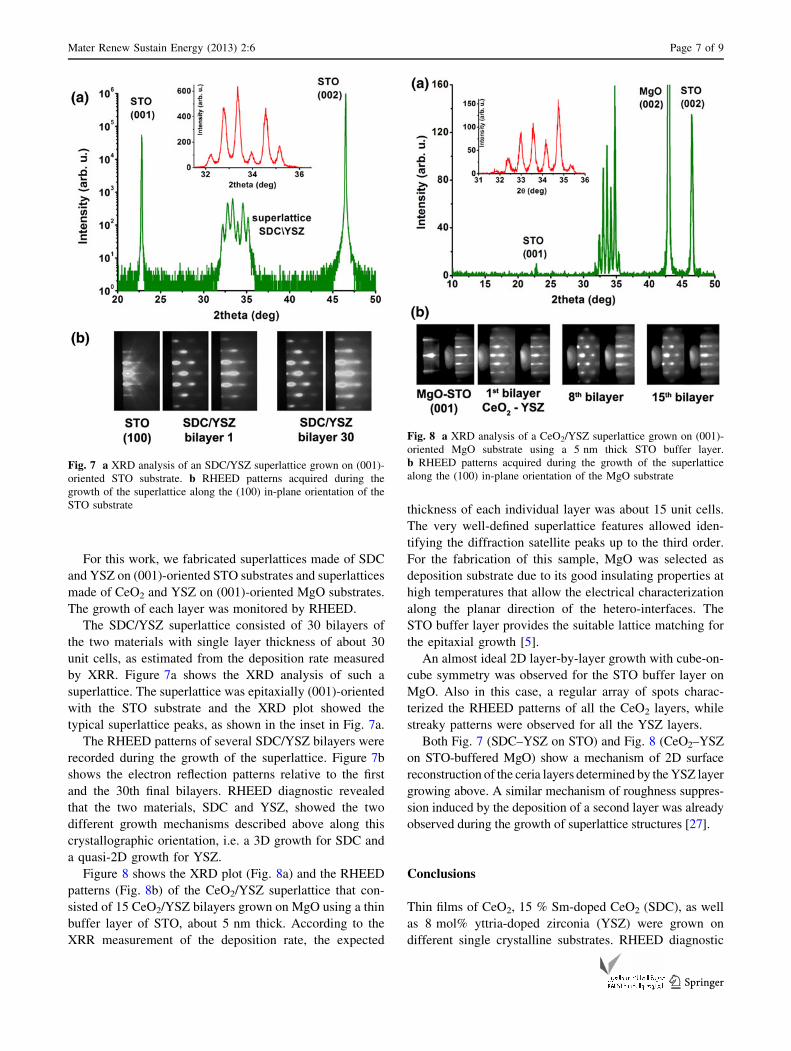
For this work, we fabricated superlattices made of SDC
and YSZ on (001)-oriented STO substrates and superlattices
made of CeO2 and YSZ on (001)-oriented MgO substrates.
The growth of each layer was monitored by RHEED.
The SDC/YSZ superlattice consisted of 30 bilayers of
the two materials with single layer thickness of about 30
unit cells, as estimated from the deposition rate measured
by XRR. Figure 7a shows the XRD analysis of such a
superlattice. The superlattice was epitaxially (001)-oriented
with the STO substrate and the XRD plot showed the
typical superlattice peaks, as shown in the inset in Fig. 7a.
The RHEED patterns of several SDC/YSZ bilayers were
recorded during the growth of the superlattice. Figure 7b
shows the electron reflection patterns relative to the first
and the 30th final bilayers. RHEED diagnostic revealed
that the two materials, SDC and YSZ, showed the two
different growth mechanisms described above along this
crystallographic orientation, i.e. a 3D growth for SDC and
a quasi-2D growth for YSZ.
Figure 8 shows the XRD plot (Fig. 8a) and the RHEED
patterns (Fig. 8b) of the CeO2/YSZ superlattice that con-
sisted of 15 CeO2/YSZ bilayers grown on MgO using a thin
buffer layer of STO, about 5 nm thick. According to the
XRR measurement of the deposition rate, the expected
thickness of each individual layer was about 15 unit cells.
The very well-defined superlattice features allowed iden-
tifying the diffraction satellite peaks up to the third order.
For the fabrication of this sample, MgO was selected as
deposition substrate due to its good insulating properties at
high temperatures that allow the electrical characterization
along the planar direction of the hetero-interfaces. The
STO buffer layer provides the suitable lattice matching for
the epitaxial growth [5].
An almost ideal 2D layer-by-layer growth with cube-on-
cube symmetry was observed for the STO buffer layer on
MgO. Also in this case, a regular array of spots charac-
terized the RHEED patterns of all the CeO2 layers, while
streaky patterns were observed for all the YSZ layers.
Both Fig. 7 (SDC–YSZ on STO) and Fig. 8 (CeO2–YSZ
on STO-buffered MgO) show a mechanism of 2D surface
reconstruction of the ceria layers determined by the YSZ layer
growing above. A similar mechanism of roughness suppres-
sion induced by the deposition of a second layer was already
observed during the growth of superlattice structures [27].
Conclusions
Thin films of CeO2, 15 % Sm-doped CeO2 (SDC), as well
as 8 mol% yttria-doped zirconia (YSZ) were grown on
different single crystalline substrates. RHEED diagnostic
Fig. 7 a XRD analysis of an SDC/YSZ superlattice grown on (001)-
oriented STO substrate. b RHEED patterns acquired during the
growth of the superlattice along the (100) in-plane orientation of the
STO substrate
Fig. 8 a XRD analysis of a CeO2/YSZ superlattice grown on (001)-
oriented MgO substrate using a 5 nm thick STO buffer layer.
b RHEED patterns acquired during the growth of the superlattice
along the (100) in-plane orientation of the MgO substrate
Mater Renew Sustain Energy (2013) 2:6 Page 7 of 9
123

allowed identifying two distinct growth mechanisms for
the ceria films along the (001) and (111) growth directions.
A 3D growth mechanism, associated with a more pro-
nounced surface roughness, clearly characterized the
growth of the (001)-oriented surfaces, while a quasi-2D
growth was observed for the (111)-oriented surfaces. The
3D (001)-oriented growth of CeO2 and SDC was observed
over a relatively wide range of deposition temperatures,
laser energy densities, oxygen background pressures, and
deposition rates, suggesting that this growth mechanism is
intrinsically related with the physicochemical properties of
this material. On the contrary, YSZ films showed an almost
ideal 2D layer-by-layer growth along the (001) orientation,
even in the presence of relatively unfavourable crystalline
matching with the substrate, such as in the case of films
grown on MgO.
The two distinct growth mechanisms along the (001)
orientation were, to the best of our knowledge, for the first
time correlated with the low index surface Gibbs free
energies of the two materials, computed by first-principles
DFT. Our calculation showed that both crystalline struc-
tures favour the (111) surface that strongly minimizes the
Gibbs free energy, but the difference between the (001) and
(111) surface energies of CeO2 is twice that of cubic ZrO2.
The enhanced roughness of the (001)-oriented doped or
undoped CeO2 surfaces should be taken into account in
particular as far as the growth of highly textured multi-
layered hetero-structures is concerned. In this work, we
have shown that the ceria-based layers preserve their
characteristic 3D growth mechanism also when comprised
in super-structures with YSZ leading to potentially signif-
icant effects on the interface morphology. Therefore,
especially for CeO2 and SDC, much better surface (and
interface) quality might be achieved by developing the
expertise needed to obtain coherent film epitaxy and biaxial
texture along less common crystallographic directions, for
instance on pseudo-cubic (110)- or (111)-oriented surfaces.
Acknowledgments This work was partly supported by the World
Premier International Research Centre Initiative of MEXT, Japan.
Open Access This article is distributed under the terms of the
Creative Commons Attribution License which permits any use, dis-
tribution, and reproduction in any medium, provided the original
author(s) and the source are credited.
References
1. Esposito, V., Traversa, E.: Design of electroceramics for solid
oxides fuel cell applications: playing with ceria. J. Am. Ceram.
Soc. 91, 1037–1051 (2008)
2. Wachsman, E.D., Lee, K.Y.: Lowering the temperature of solid
oxide fuel cells. Science 334, 935–939 (2011)
3. Chen, L.B.: Yttria-stabilized zirconia thermal barrier coatings—a
review. Surf. Rev. Lett. 13, 535–544 (2006)
4. Trovarelli, A.: Catalysis by ceria and related materials. In: Cat-
alytic science series, vol. 2. World Scientific Publishing Co,
Singapore (2002)
5. Sanna, S., Esposito, V., Pergolesi, D., Orsini, A., Tebano, A.,
Licoccia, S., Balestrino, G., Traversa, E.: Fabrication and elec-
trochemical properties of epitaxial samarium-doped ceria films
on SrTiO3-buffered MgO substrates. Adv. Funct. Mater. 19,
1713–1719 (2009)
6. Goebel, M.C., Gregori, G., Guo, X., Maier, J.: Boundary effects
on the electrical conductivity of pure and doped cerium oxide thin
films. Phys. Chem. Chem. Phys. 12, 14351–14361 (2010)
7. Goebel, M.C., Gregori, G., Maier, J.: Mixed conductivity in
nanocrystalline highly acceptor doped cerium oxide thin films
under oxidizing conditions. Phys. Chem. Chem. Phys. 13, 10940–
10945 (2011)
8. Sillassen, M., Eklund, P., Pryds, N., Johnson, E., Helmersson, U.,
Bøttiger, J.: Low-temperature superionic conductivity in strained
yttria-stabilized zirconia. Adv. Funct. Mater. 20, 2071–2076
(2010)
9. Korte, C., Peters, A., Janek, J., Hesse, D., Zakharov, N.: Ionic
conductivity and activation energy for oxygen ion transport
in superlattices—the semicoherent multilayer system YSZ
(ZrO2 ? 9.5 mol% Y2O3)/Y2O3. Phys. Chem. Chem. Phys. 10,
4623–4635 (2008)
10. Azad, S., Marina, O.A., Wang, C.M., Saraf, L., Shutthanandan,
V., McCready, D.E., El-Azab, A., Jaffe, J.E., Engelhard, M.H.,
Peden, C.H.F., Thevuthasan, S.: Nanoscale effects on ion con-
ductance of layer-by-layer structures of gadolinia-doped ceria and
zirconia. Appl. Phys. Lett. 86, 1319061 (2005)
11. Korte, C., Schichtel, N., Hesse, D., Janek, J.: Influence of inter-
face structure on mass transport in phase boundaries between
different ionic materials. Monatsh. Chem. 140, 1069–1080 (2009)
12. Schichtel, N., Korte, C., Hesse, D., Zakharov, N., Butz, B.,
Gerthsenc, D., Janek, J.: On the influence of strain on ion
transport: microstructure and ionic conductivity of nanoscale
YSZ/Sc2O3 multilayers. Phys. Chem. Chem. Phys. 12, 14596–
14608 (2010)
13. Wang, C.M., Thevuthasan, S., Peden, C.H.F.: Interface structure
of an epitaxial cubic ceria film on cubic zirconia. J. Am. Ceram.
Soc. 86, 363–365 (2003)
14. Ikegawa, S., Motoi, Y.: Growth of CeO2 thin films by metal-
organic molecular beam epitaxy. Thin Solid Films 281, 60–63
(1996)
15. Zaitsev, A.G., Ockenfuss, G., Guggi, D., Wordenweber, R.,
Kruger, U.: Structural perfection of (001) CeO2 thin films on
(1102) sapphire. J. Appl. Phys. 81, 3069–3072 (1997)
16. Bera, D., Kuchibhatla, S.V.N.T., Azad, S., Saraf, L., Wang, C.M.,
Shutthanandan, V., Nachimuthu, P., McCready, D.E., Engelhard,
M.H., Marina, O.A., Baer, D.R., Seal, S., Thevuthasan, S.:
Growth and characterization of highly oriented gadolinia-doped
ceria (111) thin films on zirconia (111)/sapphire (0001) sub-
strates. Thin Solid Films 516, 6088–6094 (2008)
17. Kurian, J., Naito, M.: Growth of epitaxial CeO2 thin films on
r-cut sapphire by molecular beam epitaxy. Physica C 492, 31–37
(2004)
18. Nandasiri, M.I., Nachimuthu, P., Varga, T., Shutthanandan, V.,
Jiang, W., Kuchibhatla, S.V.N.T., Thevuthasan, S., Seal, S.,
Kayani, A.N.: Influence of growth rate on the epitaxial orienta-
tion and crystalline quality of CeO2 thin films grown on Al2O3
(0001). J. Appl. Phys. 109, 013525 (2011)
19. Manning, P.S., Sirman, J.D., De Souza, R.A., Kilner, J.A.: The
kinetics of oxygen transport in 9.5 mol % yttria stabilized zir-
conia. Solid State Ionics 100, 1–10 (1997)
Page 8 of 9 Mater Renew Sustain Energy (2013) 2:6
123

20. Fronzi, M., Soon, A., Delley, B., Traversa, E., Stampfl, C.: Sta-
bility and morphology of cerium oxide surfaces in an oxidizing
environment: a first-principles investigation. J. Chem. Phys. 131,
104701 (2009)
21. Xia, X., Oldman, R., Catlow, R.: Computational modeling study
of bulk and surface of yttria-stabilized cubic zirconia. Chem.
Mater. 21, 3576–3585 (2009)
22. Muller, P., Kern, R.: Equilibrium nano-shape change induced by
epitaxial stress: effect of surface stress. Surf. Sci. 457, 229–253
(2000)
23. Fabbri, E., Pergolesi, D., Traversa, E.: Ionic conductivity in oxide
heterostructures: the role of interfaces. Sci. Technol. Adv. Mater.
11, 054503–054512 (2010)
24. Garcia-Barriocanal, J., Rivera-Calzada, A., Varela, M., Sefrioui,
Z., Iborra, E., Leon, C., Pennycook, S.J., Santamaria, J.: Colossal
ionic conductivity at interfaces of epitaxial ZrO2:Y2O3/SrTiO3
heterostructures. Science 321, 676–680 (2008)
25. Pergolesi, D., Tebano, A., Fabbri, E., Balestrino, G., Licoccia, S.,
Traversa, E.: Pulsed lased deposition of superlattices based on
ceria and zirconia. ECS Trans. 35, 1125–1130 (2010)
26. Pergolesi, D., Fabbri, E., Cook, S.N., Roddatis, V., Traversa, E.,
Kilner, J.A.: Tensile lattice distortion does not affect oxygen
transport in yttria-stabilized zirconia-CeO2 heterointerfaces. ACS
Nano (2012). doi:10.1021/nn302812m
27. Tebano, A., Balestrino, G., Lavanga, S., Martellucci, S., Meda-
glia, P.G., Paoletti, A., Pasquini, G., Petrocelli, G., Tucciarone,
A.: Reflection high-energy electron diffraction oscillations during
epitaxial growth of artificially layered films of (BaCuOx)m/
(CaCuO2)n. Physica C 355, 335–340 (2001)
Mater Renew Sustain Energy (2013) 2:6 Page 9 of 9
123