FP7 CPU Unit Ver 4.20 Additional Functions Manual
45
FP7 CPU Unit Ver 4.20 Additional Functions Manual 12.21.2015
-
Upload
khangminh22 -
Category
Documents
-
view
3 -
download
0
Transcript of FP7 CPU Unit Ver 4.20 Additional Functions Manual

FP7 CPU Unit
Ver 4.20
Additional Functions Manual
12.21.2015

Table of Contents
ii
Table of Contents 1. Introduction of Ver.4.20 ..................................................... 1-1
1.1 Introduction of FP7 CPU Unit Ver.4.20 .................................................. 1-2
2. Basic Instructions .............................................................. 2-1
2.1 List of Instructions.................................................................................. 2-2
2.2 TM16 (16-bit Timer) ............................................................................... 2-3
2.3 CT16- (16-bit Counter) .......................................................................... 2-6
2.4 Precautions for Programming ................................................................ 2-9
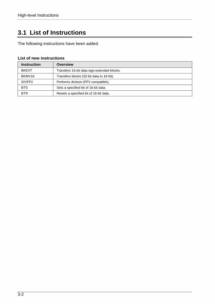
3. High-level Instructions ...................................................... 3-1
3.1 List of Instructions.................................................................................. 3-2
3.2 BKEXT (16-bit Data Sign-extended Block Move) ................................... 3-3
3.3 BKMV16 (Block Move (32-bit Data to 16-bit Data)) ................................ 3-5
3.4 DIVFP2 (Division (FP2 Compatible)) ..................................................... 3-7
3.5 BTS (16-bit Data Specified Bit Set) ........................................................ 3-9
3.6 BTR (16-bit Data Specified Bit Reset) .................................................. 3-11
4. FP2/FP2SH Program Conversion Function ...................... 4-1
4.1 List of Conversion Instructions to FP7 ................................................... 4-2
4.2 Conversion of Special Relays ................................................................ 4-5
4.3 Conversion of Special Data Registers ................................................... 4-7
5. MEWTOCOL-COM .............................................................. 5-1
5.1 List of Commands.................................................................................. 5-2
6. Multi Connection Server Function .................................... 6-1
6.1 Multi Connection Server Function .......................................................... 6-2
6.1.1 Setting Conditions and Operating Conditions ......................................... 6-2
6.1.2 Precautions When Connecting Multi Connection Servers ...................... 6-4
6.2 How to Set Connections ........................................................................ 6-5

1 Introduction of Ver.4.20

Introduction of Ver.4.20
1-2
1.1 Introduction of FP7 CPU Unit Ver.4.20
The following functions have been added to FP7 CPU Unit Ver.4.20.
Additional functions
1. Instructions and communication commands which are convenient for migrating to FP7 CPU Unit from FP2 CPU Unit have been added.
Basic instructions TM16,CT16-
* For details, refer to Chapter 2 Basic Instructions.
High-level instructions BKEXT,BKMV16,DIVFP2, BTS,BTR
* For details, refer to Chapter 3 High-level Instructions.
MEWTOCOL-COM RS,WS,RK,WK
* For details, refer to Chapter 5 MEWTOCOL-COM.
2. The following functions have been added to the Ethernet function.
Multi connection server function
Using this function, multiple devices can be connected to the same communication port.
For example, this function can be used for the following slave communications;
MODBUS-TCP (Port number 502)
MC protocol (Port number 5000)
MEWTOCOL-COM or MEWTOCOL7-COM
* For details, refer to 6 Multi Connection Server Function.

1.1 Introduction of FP7 CPU Unit Ver.4.20
1-3
Version for each model number
Model number Production lot until March, 2014
Production lot from April, 2014
AFP7CPS21 Ver. 1.20
AFP7CPS41E(S) Ver. 3.42 Ver. 4.20
AFP7CPS31(E)(S)
NOTE
The AFP7CPS41E(S) and AFP7CPS31(E)(S) manufactured before March, 2014 cannot be upgraded to Ver.4.20.
How to confirm the production lot
The date of the production lot can be confirmed from the lot number of FP7.
The number is indicated on the side face of the FP7 CPU unit (on which a unit is installed).
FP7 CPU Unit
151101
1511012
3 151101
FP7 CPU Unit (Side face)
FP
7C
PU
U
NIT
AF
P7
CP
S4
1E
SM
odel
No.
In the case of the above AFP7CPS41ES, the lot number is "151101".
This indicates that the unit was manufactured on "November 1, 2015". As the production date is after April, 2014, this unit will be upgraded to Ver.4.20.


2 Basic Instructions

Basic Instructions
2-2
2.1 List of Instructions
The following instructions have been added.
List of new instructions
Instruction Overview
TM16 Subtraction timer of 16-bit setting value
CT16- Subtraction preset counter of 16-bit setting value

2.2 TM16 (16-bit Timer)
2-3
2.2 TM16 (16-bit Timer)
Instruction format
TM16X5
U30
n S
R0
T5 Y111
Operation unit (i)
There is no operation unit.
List of operands
Operand Description
n Timer number (Settalbe range: 0 to 4095 *For the default memory configuration)
S Timer setting value (Settable range: U0 to U65535)
Available devices (●: Available)
Operand
16-bit device 32-bit device Integer Real
number String
Index modifier
*1 WX WY WR WL WS SD DT LD UM WI WO
TS
CS
TE
CE IX K U H SF DF " "
n ● ●
S ● ● ● ● ● ● ● ●
*1:Only 16-bit deivces, 32-bit devices, and integer constants can be modified. (Real number constants and character constants cannot be specified.)
Outline of operation
This instruction is different from TIM instruction. The range settable by the setting value [S] is U0 to U65535.
The timer is a non-hold type that is reset when the power supply is turned off or the RUN mode is switched to the PROG. mode.
When the execution condition is ON, subtraction is carried out for the specified time [S], and when the elapsed value reaches U0, the timer contact [Tn] (n is a timer contact number) turns ON.
When the execution condition turns OFF during the subtraction operation, the elapsed value is reset (cleared to zero).
It is also possible to describe OT instruction right after the timer coil.

Basic Instructions
2-4
For details of this instruction, refer to the description of TM instruction in FP7 CPU Unit Programming Manual.
- The setting time of the timer is (Timer unit) x (Timer setting value).
"TM16S" is 0.00000 to 0.65535 seconds by 0.00001 seconds.
"TM16L" is 0.000 to 65.535 seconds by 0.001 seconds.
"TM16R" is 0.00 to 655.35 seconds by 0.01 seconds.
"TM16X" is 0.0 to 6553.5 seconds by 0.1 seconds.
"TM16Y" is 0 to 65535 seconds by 1 second.
Difference between TIM and TM16 instructions
When specifying a 16-bit device
DT0 U1
DT1 U2
- TM instruction
TMX0 DT0
R0
T0 Y111
DT0 DT1
U1 U2
TE0
U131073
DT0 is treated as 32-bit data U131073(H20001).
U131073 is set in the elapsed value area TE0 when the input of R0 rises.
- TM16 instruction
TM16X0
DT0
R0
T0 Y111
DT0
U1
TE0
U1
DT0 is treated as 16-bit data U1(H1).
U1 is set in the elapsed value area TE0 when the input of R0 rises.
Note)
When a 32-bit value is written into the elapsed value area TE while the timer is being operated using an instruction such as MV instruction, the timer operates with the written 32-bit value.

2.2 TM16 (16-bit Timer)
2-5
When specifying a constant
- TM instruction
TMX0 U100
R0
T0 Y111TE0
U100
TS0
U100
U100 is set in the setting value area TS0 when compiling the program.
The setting value area TS0 is set in the elapsed value area TE0 when the input of R0 rises.
The setting range of a constant is U0 to U4294967295.
- TM16 instruction
TM16X0
U100
R0
T0 Y111TE0
U100
TS0
U100
U100 is set in the setting value area TS0 when compiling the program.
The setting value area TS0 is set in the elapsed value area TE0 when the input of R0 rises.
The setting range of a constant is U0 to U65535.
Note)
When a 32-bit value is written into the elapsed value area TE while the timer is being operated using an instruction such as MV instruction, the timer operates with the written 32-bit value.
When a 32-bit value is written into the setting value area TS, the timer operates with the written 32-bit value.
Precautions during programming
Both the timer setting value area TS and the timer elapsed value area TE occupy the 32-bit area.
When specifying a 16-bit device such as DT for the operation [S] of TM16 instruction, it is used as 16-bit data.
As subtraction is performed during an arithmetic operation, create a program to subtract once during one scan time. Correct results cannot be acquired when subtraction operation is performed several times during one scan due to an interrupt program or the jump/loop instruction, or when subtraction cannot be performed.
When U0 is specified for the setting value, the timeout operation is performed when the instruction is executed and the timer contact [T] turns ON.
Please be aware that the program is not described incorrectly when combining the timer instruction with the and stack instruction or pop stack instruction. (For details, refer to 2.4 Precautions for Programming.)

Basic Instructions
2-6
2.3 CT16- (16-bit Counter)
Instruction format
CT16-100
U10
n
S
X100
C100 Y131
X101
Count
Reset
Operation unit (i)
There is no operation unit.
List of operands
Operand Description
n Counter number (Settalbe range: 0 to 1023 *For the default memory configuration)
S Counter setting value (Settable range: U0 to U65535)
Available devices (●: Available)
Operand
16-bit device 32-bit device Integer Real
number String Index
modifier *1 WX WY WR WL WS SD DT LD UM WI WO
TS
CS
TE
CE IX K U H SF DF " "
n ● ●
S ● ● ● ● ● ● ● ●
*1:Only 16-bit deivces, 32-bit devices, and integer constants can be modified. (Real number constants and character constants cannot be specified.)
Outline of operation
This instruction is different from CT instruction. The range settable by the setting value [S] is U0 to U65535.
All counters are subtraction preset counters.
When the reset input is switched from ON to OFF, the value of the setting value area CS is preset in the elapsed value area CE.
When the reset input is on, the elapsed value is reset (cleared to zero). When the count input changes from the off state to the on state, the setting value is subtracted. When the elapsed value becomes U0, it is output to the counter contact.
When the count input and reset input turn on simultaneously, the reset input has priority.
When the rise of the count input and the fall of the reset input are detected at the same time, the count input is ignored and only the preset is executed.
It is also possible to describe OT instruction right after the counter instruction.
For details of this instruction, refer to the description of CT instruction in FP7 CPU Unit Programming Manual.

2.3 CT16- (16-bit Counter)
2-7
Difference between CT and CT16- instructions
When specifying a 16-bit device
DT0 U1
DT1 U2
- CT instruction
CT0
DT0
X100
C0 Y131
X101
Count
Reset
DT0 DT1
U1 U2
CE0
U131073
DT0 is treated as 32-bit data U131073(H20001).
U131073 is set in the elapsed value area CE0 when the input of X101 falls.
- CT16- instruction
CT16-0
DT0
X100
C0 Y131
X101
Count
Reset
DT0
U1
CE0
U1
DT0 is treated as 16-bit data U1(H1).
U1 is set in the elapsed value area CE0 when the input of X101 falls.
Note)
When a 32-bit value is written into the elapsed value area CE while the counter is being operated using an instruction such as MV instruction, the timer operates with the written 32-bit value.

Basic Instructions
2-8
When specifying a constant
- CT instruction
CT0
U100
X100
C0 Y131
X101
Count
Reset
CE0
U100
CS0
U100
U100 is set in the setting value area CS0 when compiling the program.
The setting value area CS0 is set in the elapsed value area CE0 when the input of X101 falls.
The setting range of a constant is U0 to U4294967295.
- CT16- instruction
CT16-0
U100
X100
C0 Y131
X101
Count
Reset
CE0
U100
CS0
U100
U100 is set in the setting value area CS0 when compiling the program.
The setting value area CS0 is set in the elapsed value area CE0 when the input of X101 falls.
The setting range of a constant is U0 to U65535.
Note)
When a 32-bit value is written into the elapsed value area CE while the counter is being operated using an instruction such as MV instruction, the timer operates with the written 32-bit value.
When a 32-bit value is written into the setting value area CS, the timer operates with the written 32-bit value.
Precautions during programming
Both the counter setting value area CS and the counter elapsed value area CE occupy the 32-bit area.
When specifying a 16-bit device such as DT for the operation [S] of CT16- instruction, it is used as 16-bit data.
When U0 is specified for the setting value, the count-up operation is performed when the instruction is executed and the counter contact [C] turns ON.

2.4 Precautions for Programming
2-9
2.4 Precautions for Programming
Programs which are not executed correctly
Do no write the following programs as they are not executed correctly.
Example 1) When X101 is ON prior to X100, Y100 does not turn on even when X100 turns ON.
X100 Y100
ANSX101
X102
DF
Example 2) TMX16X0 activates when X101 turns on regardless of whether X0 is on or off.
TM16X0
U30
X100 Y100
ANSX101
X102
Example 3) When X102 is ON prior to X100, Y101 does not turn on even when X100 turns ON.
X100
Y101
PSHSX101
X102
DF
X103
Y100
ANS
When a combination of contacts are set as the trigger (execution condition) of a differential instruction (DF) or timer instruction, do not use ANS instruction, RDS instruction, or POPS instruction.
Examples in which the above programs are rewritten

Basic Instructions
2-10
The followings are the examples.
Program in which the example 1 is rewritten
X100 Y100X101
X102
DF
X100
Program in which the example 2 is rewritten
TM16X0
U30
X100 Y100X101
X102X100
Program in which the example 3 is rewritten
X100
Y101
X101
X102
DF
X103
Y100
X100
X100
The following program normally operates.
X100
DF
Y100
Y101
U30
TMY1 U20
TM16X0

3 High-level Instructions
High-level Instructions
3-2
3.1 List of Instructions
The following instructions have been added.
List of new instructions
Instruction Overview
BKEXT Transfers 16-bit data sign-extended blocks.
BKMV16 Transfers blocks (32-bit data to 16-bit).
DIVFP2 Performs division (FP2 compatible).
BTS Sets a specified bit of 16-bit data.
BTR Resets a specified bit of 16-bit data.

3.2 BKEXT (16-bit Data Sign-extended Block Move)
3-3
3.2 BKEXT (16-bit Data Sign-extended Block Move)
Instruction format
BKEXT.US DT2 DT3
S2 D
R0
DT0
S1i
Operation unit (●: Available)
Operation unit
bit US SS UL SL SF DF
i ● ●
List of operands
Operand Description
S1 The starting address of the device storing the data that sign extension is performed.
S2 The ending address of the device storing the data that sign extension is performed.
D Destination starting device address
Available devices (●: Available)
Operand
16-bit device 32-bit device Integer Real
number String
Index modifier
*1 WX WY WR WL WS SD DT LD UM WI WO
TS
CS
TE
CE IX K U H SF DF " "
S1 ● ● ● ● ● ● ● ● ●
S2 ● ● ● ● ● ● ● ● ●
D ● ● ● ● ● ● ● ● ● ●
*1:Only 16-bit deivces, 32-bit devices, and integer constants can be modified. (Real number constants and character constants cannot be specified.)
Outline of operation
Performs sign extension for device values in the area specified by [S1] to [S2], and transfers them to the device address specified by [D] and subsequent addresses.

High-level Instructions
3-4
Processing
Example 1) When the operation unit is signed 16-bit (SS)
S1: DT0, S2: DT3, D: DT10
DT0 -2(FFFEh) DT10 ・DT11 -2(FFFFFFFEh)
DT1 -1(FFFFh) DT12 ・DT13 -1(FFFFFFFFh)
DT2 0(0000h) DT14 ・DT15 0(00000000h)
DT3 1(0001h) DT16 ・DT17 1(00000001h)
DT4 DT18 ・DT19
Example 2) When the operation unit is unsigned 16-bit (US)
S1: DT0, S2: DT3, D: TS0
DT0 65534(FFFEh) TS0 65534(0000FFFEh)
DT1 65535(FFFFh) TS1 65535(0000FFFFh)
DT2 0(0000h) TS2 0(00000000h)
DT3 1(0001h) TS3 1(00000001h)
DT4 TS4
Precautions during programming
In the case of a direct address and index modification address, specify the same type of device for [S1] and [S2]. Besides, specify [S2] to be equal to or larger than [S1].
The specified source area and destination area should not overlap each other.
Flag operation
Name Description
Latest error (SR7)
Hold error (SR8)
To be set in case of out-of-range in indirect access (index modiication).
To be set when S1 is larger than S2.
To be set when the destination range is out of the accessible range.
To be set when the ranges of the source area and the destination area overlap.
3.3 BKMV16 (Block Move (32-bit Data to 16-bit Data))
3-5
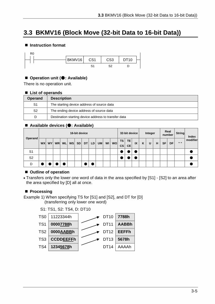
3.3 BKMV16 (Block Move (32-bit Data to 16-bit Data))
Instruction format
BKMV16 CS3 DT10
S2 D
R0
CS1
S1
Operation unit (●: Available)
There is no operation unit.
List of operands
Operand Description
S1 The starting device address of source data
S2 The ending device address of source data
D Destination starting device address to transfer data
Available devices (●: Available)
Operand
16-bit device 32-bit device Integer Real
number String
Index modifier
WX WY WR WL WS SD DT LD UM WI WO TS
CS
TE
CE IX K U H SF DF " "
S1 ● ● ● ●
S2 ● ● ● ●
D ● ● ● ● ● ● ●
Outline of operation
Transfers only the lower one word of data in the area specified by [S1] - [S2] to an area after the area specified by [D] all at once.
Processing
Example 1) When specifying TS for [S1] and [S2], and DT for [D] (transferring only lower one word)
S1: TS1, S2: TS4, D: DT10
TS0 11223344h DT10 7788h
TS1 00007788h DT11 AABBh
TS2 0000AABBh DT12 EEFFh
TS3 CCDDEEFFh DT13 5678h
TS4 12345678h DT14 AAAAh

High-level Instructions
3-6
Example 2) When specifying TS for [S1] and [S2], and LD for [D] (transferring only lower one word)
S1: TS5, S2: TS7, D: LD20
TS4 11112222h LD20 4444h
TS5 00004444h LD21 6666h
TS6 55556666h LD22 8888h
TS7 77778888h LD23 1234h
TS8 9999AAAAh LD24 5678h
Precautions during programming
In the case of a direct address and index modification address, specify the same type of device for [S1] and [S2]. Besides, specify [S2] to be equal to or larger than [S1].
Flag operation
Name Description
Latest error (SR7)
Hold error (SR8)
To be set in case of out-of-range values in indirect access (index modification, pointer access).
To be set when S1 is larger than S2.
To be set when the destination range is out of the accessible range.

3.4 DIVFP2 (Division (FP2 Compatible))
3-7
3.4 DIVFP2 (Division (FP2 Compatible))
Instruction format
DIVFP2.US DT2 DT3
S2 D
R0
DT0
S1i
Operation unit (●: Available)
Operation unit bit US SS UL SL SF DF
i ● ● ● ●
List of operands
Operand Description
S1 Target data 1 for operation (Device address or constant)
S2 Target data 2 for operation (Device address or constant)
D Operation result data (Device address)
Available devices (●: Available)
Operand
16-bit device 32-bit device
*1 Integer
Real number
String Index
modifier *2
WX WY WR WL WS SD DT LD UM WI WO TS
CS
TE
CE
IX *3
K *4
U *5
H *6
SF DF " "
S1 ● ● ● ● ● ● ● ● ● ● ● ● ● ● ● ● ● ●
S2 ● ● ● ● ● ● ● ● ● ● ● ● ● ● ● ● ● ●
D ● ● ● ● ● ● ● ● ● ● ● ●
*1: Cannot be specified when the operation unit is 16-bit integer (SS, US).
*2: Only 16-bit deivces, 32-bit devices, and integer constants can be modified. (Real number constants and character constants cannot be specified.)
*3: Index registers (I0 to IE)
*4: Can be specified only when the operation unit is signed integer (SS, SL).
*5: Can be specified only when the operation unit is unsigned integer (US, UL).
*6: Can be specified only when the operation unit is integer (US, SS, UL, SL).
Outline of operation
Divides [S1] by the value of [S2] according to the operation unit of [i], and sets the quotient in [D] and the remainder in the system register (SD).
Operation results are stored as follows according to operation units. US, SS : (S1) / (S2) -> Quotient (D), Remainder (SD15) UL, SL : (S1+1, S1) / (S2+1, S2) -> Quotient (D+1, D), Remainder (SD16, SD15)
When an interrupt PB and interrupt program (INTPG) occur, SD15 and SD16 are automatically saved and restored. Therefore, even when this instruction is used during an interrupt program, SD15 and SD16 are not damaged. However, when using this instruction during an interrupt program, the use of SD15 and SD16 must be finished before the completion of the interrupt program.

High-level Instructions
3-8
Processing
Divides the target data 1 for operation by the target data 2, and sets the operation result data and remainder.
Example 1) When the operation unit is 16-bit (US, SS)
S1: DT2, S2: DT1, D: DT3
DT0 1 DT0 1
DT1 9 DT1 9
DT2 25 DT2 25
DT3 49 DT3 2 (Quotient)
SD15 0 SD15 7 (Remainder)
Example 2) When the operation unit is 32-bit (UL, SL)
S1:TS3, S2: TS1, D: TS10
TS0 1 TS10 5 (Quotient)
TS1 9 TS11 0
TS2 25 TS12 0
TS3 49 TS13 0
SD15 0 SD15 4 (Remainder)
SD16 0 SD16 0
Precautions during programming
When a division overflow occurs, the data is output as follows. (When the negative min. value / -1)
Operation unit SS: S1 = -32768(H8000) S2 = -1(HFFFF)
D = -32768(H8000) SD15 = 0(H0000)
Operation unit SL: S1 = -2147483648(H80000000) S2 = -1(HFFFFFFFF)
D = -2147483648(H80000000) SD15 = 0(H00000000)
Flag operation
Name Description
Latest error (SR7)
Hold error (SR8)
To be set in case of out-of-range values in indirect access (index modification, pointer access).
To be set when zero is specified for [S2].
3.5 BTS (16-bit Data Specified Bit Set)
3-9
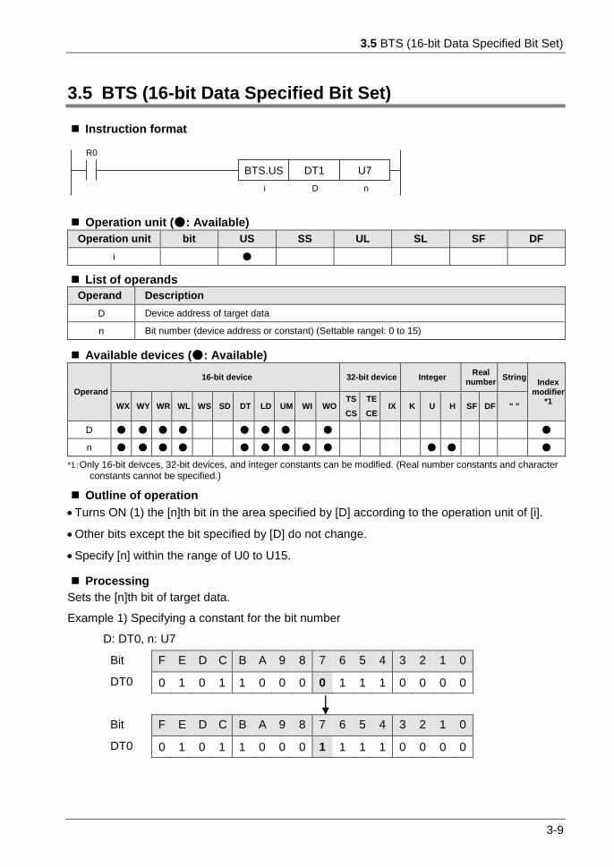
3.5 BTS (16-bit Data Specified Bit Set)
Instruction format
DT1 U7
D n
R0
BTS.US
i
Operation unit (●: Available)
Operation unit bit US SS UL SL SF DF
i ●
List of operands
Operand Description
D Device address of target data
n Bit number (device address or constant) (Settable rangel: 0 to 15)
Available devices (●: Available)
Operand
16-bit device 32-bit device Integer Real
number String
Index modifier
*1 WX WY WR WL WS SD DT LD UM WI WO
TS
CS
TE
CE IX K U H SF DF " "
D ● ● ● ● ● ● ● ● ●
n ● ● ● ● ● ● ● ● ● ● ● ●
*1:Only 16-bit deivces, 32-bit devices, and integer constants can be modified. (Real number constants and character constants cannot be specified.)
Outline of operation
Turns ON (1) the [n]th bit in the area specified by [D] according to the operation unit of [i].
Other bits except the bit specified by [D] do not change.
Specify [n] within the range of U0 to U15.
Processing
Sets the [n]th bit of target data.
Example 1) Specifying a constant for the bit number
D: DT0, n: U7
Bit F E D C B A 9 8 7 6 5 4 3 2 1 0
DT0 0 1 0 1 1 0 0 0 0 1 1 1 0 0 0 0
Bit F E D C B A 9 8 7 6 5 4 3 2 1 0
DT0 0 1 0 1 1 0 0 0 1 1 1 1 0 0 0 0

High-level Instructions
3-10
Example 2) Specifying a device for the bit number
D: DT1, n: DT0
Bit F E D C B A 9 8 7 6 5 4 3 2 1 0
DT0 0 0 0 0 0 0 0 0 0 0 0 0 1 0 0 0 U8
DT1 0 1 0 1 1 0 0 0 0 1 1 1 0 0 0 0
Bit F E D C B A 9 8 7 6 5 4 3 2 1 0
DT1 0 1 0 1 1 0 0 1 0 1 1 1 0 0 0 0
Precautions during programming
Difference between the FP7 and conventional models (such as FP2 or FP2SH); The conventional models operate with only the lower four bits as valid even when the specified [n] is out of the settable range. For the FP7, an operation error occurs when the specified value is out of the range.
Flag operation
Name Description
Latest error (SR7)
Hold error (SR8)
To be set in case of out-of-range values in indirect access (index modification, pointer access).
To be set when [n] is out of the range.
3.6 BTR (16-bit Data Specified Bit Reset)
3-11
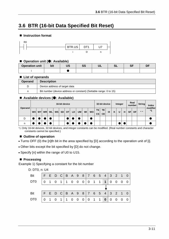
3.6 BTR (16-bit Data Specified Bit Reset)
Instruction format
DT1 U7
D n
R0
BTR.US
i
Operation unit (●: Available)
Operation unit bit US SS UL SL SF DF
i ●
List of operands
Operand Description
D Device address of target data
n Bit number (device address or constant) (Settable range: 0 to 15)
Available devices (●: Available)
Operand
16-bit device 32-bit device Integer Real
number String
Index modifier
*1 WX WY WR WL WS SD DT LD UM WI WO
TS
CS
TE
CE IX K U H SF DF " "
D ● ● ● ● ● ● ● ● ●
n ● ● ● ● ● ● ● ● ● ● ● ●
*1:Only 16-bit deivces, 32-bit devices, and integer constants can be modified. (Real number constants and character constants cannot be specified.)
Outline of operation
Turns OFF (0) the [n]th bit in the area specified by [D] according to the operation unit of [i].
Other bits except the bit specified by [D] do not change.
Specify [n] within the range of U0 to U15.
Processing
Example 1) Specifying a constant for the bit number
D: DT0, n: U4
Bit F E D C B A 9 8 7 6 5 4 3 2 1 0
DT0 0 1 0 1 1 0 0 0 0 1 1 1 0 0 0 0
Bit F E D C B A 9 8 7 6 5 4 3 2 1 0
DT0 0 1 0 1 1 0 0 0 0 1 1 0 0 0 0 0

High-level Instructions
3-12
Example 2) Specifying a device for the bit number
D: DT1, n: DT0
Bit F E D C B A 9 8 7 6 5 4 3 2 1 0
DT0 0 0 0 0 0 0 0 0 0 0 0 0 0 1 0 1 U5
DT1 0 1 0 1 1 0 0 0 0 1 1 1 0 0 0 0
Bit F E D C B A 9 8 7 6 5 4 3 2 1 0
DT1 0 1 0 1 1 0 0 0 0 1 0 1 0 0 0 0
Precautions during programming
Difference between the FP7 and conventional models (such as FP2 or FP2SH); The conventional models operate with only the lower four bits as valid even when the specified [n] is out of the settable range. For the FP7, an operation error occurs when the specified value is out of the range.
Flag operation
Name Description
Latest error (SR7)
Hold error (SR8)
To be set in case of out-of-range values in indirect access (index modification, pointer access).
To be set when [n] is out of the range.

4 FP2/FP2SH Program Conversion Function

FP2/FP2SH Program Conversion Function
4-2
4.1 List of Conversion Instructions to FP7
The patterns for converting FP2/FP2SH instructions to FP7 instructions have been changed to the following contents from the Ver.2.11.0.0 of FPWIN GR7(S).
Some instructions and operand settings cannot be converted to FP7 instructions.
For the operation when an instruction cannot be converted, refer to the following "Operation when an instruction cannot be converted".
Operation when an instruction cannot be converted
When specifying an instruction or operand that cannot be converted, the program conversion to FP7 is not performed, and the result is output to the block comment.
Example) Before converting an FP2SH program
Example) After converting the program to FP7 program
Basic instructions
FP2/FP2SH instruction FP7 instruction
Basic instruction (Boolean)
Operand condition Boolean Name
TM(X/Y/R/L) When specifying a 16-bit device for the setting value (WX/WY/WR/WL/DT/LD)
TM16
(X/Y/R/L) 16-bit timer
(*) When specifying SV/EV device for the setting value TMX
(X/Y/R/L)
Timer
(*) When specifying a constant K/H) for the setting value
CT When specifying a 16-bit device for the setting value (WX/WY/WR/WL/DT/LD)
CT16- 16-bit counter
(*) When specifying SV/EV device for the setting value
CT Counter
(*) When specifying a constant K/H) for the setting value
* : There is no change from the versions before Ver.2.10 of FPWIN GR7(S).
4.1 List of Conversion Instructions to FP7
4-3
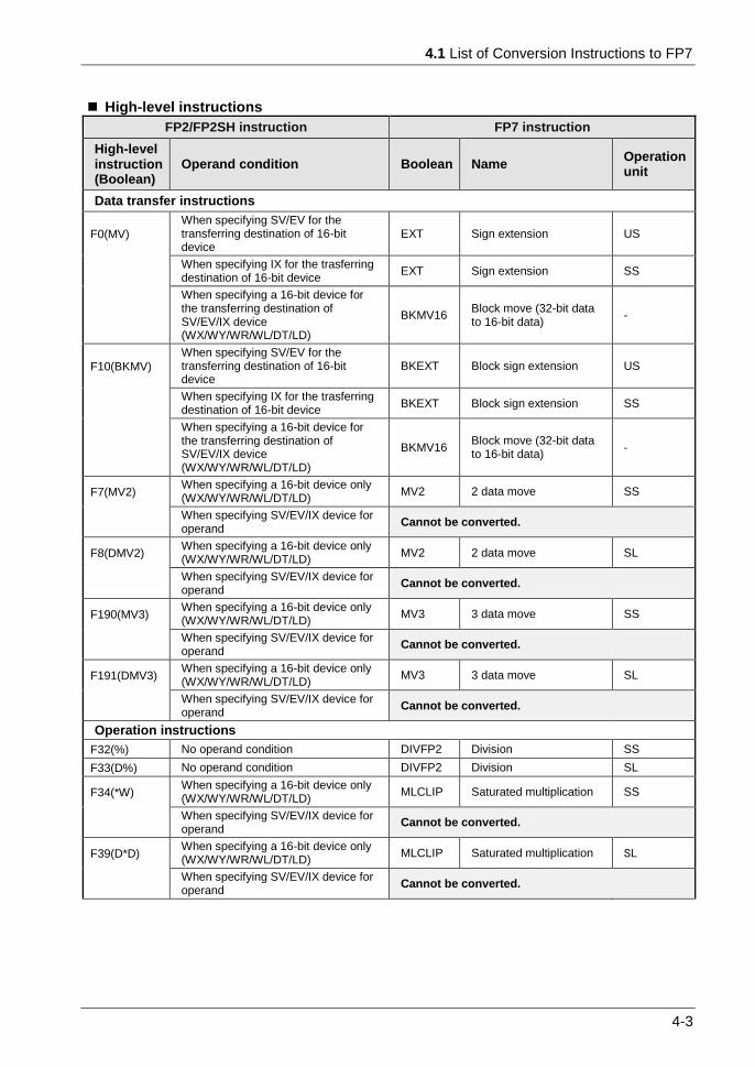
High-level instructions
FP2/FP2SH instruction FP7 instruction
High-level instruction (Boolean)
Operand condition Boolean Name Operation unit
Data transfer instructions
F0(MV)
When specifying SV/EV for the transferring destination of 16-bit device
EXT Sign extension US
When specifying IX for the trasferring destination of 16-bit device
EXT Sign extension SS
When specifying a 16-bit device for the transferring destination of SV/EV/IX device (WX/WY/WR/WL/DT/LD)
BKMV16 Block move (32-bit data to 16-bit data)
-
F10(BKMV)
When specifying SV/EV for the transferring destination of 16-bit device
BKEXT Block sign extension US
When specifying IX for the trasferring destination of 16-bit device
BKEXT Block sign extension SS
When specifying a 16-bit device for the transferring destination of SV/EV/IX device (WX/WY/WR/WL/DT/LD)
BKMV16 Block move (32-bit data to 16-bit data)
-
F7(MV2) When specifying a 16-bit device only (WX/WY/WR/WL/DT/LD)
MV2 2 data move SS
When specifying SV/EV/IX device for operand
Cannot be converted.
F8(DMV2) When specifying a 16-bit device only (WX/WY/WR/WL/DT/LD)
MV2 2 data move SL
When specifying SV/EV/IX device for operand
Cannot be converted.
F190(MV3) When specifying a 16-bit device only (WX/WY/WR/WL/DT/LD)
MV3 3 data move SS
When specifying SV/EV/IX device for operand
Cannot be converted.
F191(DMV3) When specifying a 16-bit device only (WX/WY/WR/WL/DT/LD)
MV3 3 data move SL
When specifying SV/EV/IX device for operand
Cannot be converted.
Operation instructions
F32(%) No operand condition DIVFP2 Division SS
F33(D%) No operand condition DIVFP2 Division SL
F34(*W) When specifying a 16-bit device only (WX/WY/WR/WL/DT/LD)
MLCLIP Saturated multiplication SS
When specifying SV/EV/IX device for operand
Cannot be converted.
F39(D*D) When specifying a 16-bit device only (WX/WY/WR/WL/DT/LD)
MLCLIP Saturated multiplication SL
When specifying SV/EV/IX device for operand
Cannot be converted.

FP2/FP2SH Program Conversion Function
4-4
High-level instructions
FP2/FP2SH instruction FP7 instruction
High-level instruction (Boolean)
Operand condition Boolean Name Operation unit
Bit manipulation instructions
F130(BTS) When specifying a 16-bit device only (WX/WY/WR/WL/DT/LD)
BTS Bit set US
When specifying SV/EV/IX device for operand
Cannot be converted.
F131(BTR) When specifying a 16-bit device only (WX/WY/WR/WL/DT/LD)
BTR Bit reset US
When specifying SV/EV/IX device for operand
Cannot be converted.
F132(BTI)
(*) When specifying a 16-bit device only (WX/WY/WR/WL/DT/LD)
BTI Bit Inversion US
When specifying SV/EV/IX device for operand
Cannot be converted.
F133(BTT)
(*) When specifying a 16-bit device only (WX/WY/WR/WL/DT/LD)
BTT Bit Test US
When specifying SV/EV/IX device for operand
Cannot be converted.
* : There is no change from the versions before Ver.2.10 of FPWIN GR7(S).

4.2 Conversion of Special Relays
4-5
4.2 Conversion of Special Relays
When using special relays on a conventional model, address conversion is performed in accordance with the conversion rule for converting programs to FP7.
Conversion rule
(1) Only for convertible special relays, address conversion is performed.
(2) As only similar device items are converted, the device addresses after R902C cannot be converted.
(3) Word accesses (from WR900) cannot be converted.
Operation when an instruction cannot be converted
Converts instructions leaving inconvertible device numbers unchanged, and sets "network to be excluded from execution".
Example) Before converting an FP2SH program
Example) After converting the program to FP7 program
In the above example, the device addresses R9001 to R9003, and R9005 are the output results of inconvertible items.
List of convertible special relays
Convertible special relays are as follows.
All other special relays cannot be converted.
FP2SH FP7
Device Name Device Name
R9000 Self-diagnosis error occurrence SR0 Self-diagnosis error occurrence
R9004 I/O verification error flag SR4 Unit verify error occurrence
R9007 Operation error detection (Hold) SR7 Operation error detection (Hold)
R9008 Operation error detection (Latest) SR8 Operation error detection (Latest)
R9009 CY SR9 CY
R900A > SRA >
R900B = SRB =
R900C > SRC >
R900D Auxiliary timer contact SRD Auxiliary timer contact
R900F Constant scan error flag SRF Constant scan error flag
R9010 Always ON SR10 Always ON
R9011 Always OFF SR11 Always OFF
R9012 Scan relay SR12 Scan relay
R9013 1st scan ON SR13 1st scan ON
R9014 1st scan OFF SR14 1st scan OFF
R9015 Step ladder initial ON SR15 Step ladder initial ON

FP2/FP2SH Program Conversion Function
4-6
List of convertible special relays (Continuation of the above section)
FP2SH FP7
Device Name Device Name
R9018 0.01-sec clock relay SR18 0.01-sec clock relay
R9019 0.02-sec clock relay SR19 0.02-sec clock relay
R901A 0.1-sec clock relay SR1A 0.1-sec clock relay
R901B 0.2-sec clock relay SR1B 0.2-sec clock relay
R901C 1-sec clock relay SR1C 1-sec clock relay
R901D 2-sec clock relay SR1D 2-sec clock relay
R901E 1-min clock relay SR1E 1-min clock relay
R9020 RUN mode flag SR20 CPU operation mode
R9029 Force flag SR29 Force flag
R902A Interrupt enable flag SR2A Interrupt enable flag
R902B Interrupt error flag SR2B Interrupt error flag
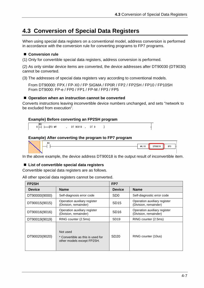
4.3 Conversion of Special Data Registers
4-7
4.3 Conversion of Special Data Registers
When using special data registers on a conventional model, address conversion is performed in accordance with the conversion rule for converting programs to FP7 programs.
Conversion rule
(1) Only for convertible special data registers, address conversion is performed.
(2) As only similar device items are converted, the device addresses after DT90030 (DT9030) cannot be converted.
(3) The addresses of special data registers vary according to conventional models.
From DT90000: FPX / FP-X0 / FP SIGMA / FP0R / FP2 / FP2SH / FP10 / FP10SH From DT9000: FP-e / FP0 / FP1 / FP-M / FP3 / FP5
Operation when an instruction cannot be converted
Converts instructions leaving inconvertible device numbers unchanged, and sets "network to be excluded from execution".
Example) Before converting an FP2SH program
Example) After converting the program to FP7 program
In the above example, the device address DT90018 is the output result of inconvertible item.
List of convertible special data registers
Convertible special data registers are as follows.
All other special data registers cannot be converted.
FP2SH FP7
Device Name Device Name
DT90000(9000) Self-diagnosis error code SD0 Self-diagnostic error code
DT90015(9015) Operation auxiliary register (Division, remainder) SD15
Operation auxiliary register (Division, remainder)
DT90016(9016) Operation auxiliary register (Division, remainder) SD16
Operation auxiliary register (Division, remainder)
DT90019(9019) RING counter (2.5ms) SD19 RING counter (2.5ms)
DT90020(9020)
Not used
* Convertible as this is used for other models except FP2SH.
SD20 RING counter (10us)


5 MEWTOCOL-COM

MEWTOCOL-COM
5-2
5.1 List of Commands
The following new commands are supported.
List of commands
Command name Code Overview
Read timer set value area RS Reads the timer set value (lower 16 bits of TS).
Write timer set value area WS Writes to the timer set value (lower 16 bits of TS). (Note 3)
Read timer elapsed value area RK Reads the timer elapsed value (lower 16 bits of TE).
Write timer elapsed value area WK Writes to the timer elapsed value (lower 16 bits of TE). (Note 3)
(Note 1) Some devices cannot be accessed due to format limitations of MEWTOCOL-COM communication commands.
(Note 2) With the four MEWTOCOL-COM commands newly supported, it is possible to access the timer and counter on the conventional models (FP2/FP2SH). On FP7, however, it is possible to access the timer only.
(Note 3) "H0000" is written to the high words of TS or TE.

6 Multi Connection Server
Function
Multi Connection Server Function
6-2
6.1 Multi Connection Server Function
Multiple devices can be connected to the same port by making connection settings in advance.
Using the multi connection server function, servers with specified port numbers of the connectable number "n" can be configured by making the same server settings for continuous "n" connections using the setting tool.
The number of settable multi connection servers are as follows; Max. 16 connections for one group, and 16 groups of servers.
Note)
When continuous sixteen connections are set, transmitted data from sixteen clients may not be received simultaneously although TCP connection is available.
The number of data the Ethernet unit can receive simultaneously is limited.
When using the EtherNet/IP communication, the maximum number of simultaneous receivable data from clients is eight. When not using the EtherNet/IP communication, it is sixteen.
When using another Ethernet communication function, the actual number may be less than the above receivable number.
6.1.1 Setting Conditions and Operating Conditions
Note the following when using this function.
1. This function is available only when "Specify IPv4 or IPv6" is set to "IPv4 only" in the Basic communications information under Built-in ET-LAN setting.
When specifying other option than "IPv4 only" and specifying the multi connection server, a unit error (warning) occurs.
2. Both system and user connections can be set.
3. When specifying "TCP/IP" for Communication type, Open type (server/client) should be set to "Server connection".
When "Client connection" is specified, a unit error occurs.
When specifying "Server connection (specific destination), select "Use IPv4" for "Destination unit IP address" as well as "Specify IPv4 or IPv6" of Basic communications information.
Using "Server connection (any destination)" is recommended.
4. This function can also be used when "UDP" is specified for Communication type
However, do not use the multi-frame communication of "MEWTOCOL7-COM" and "MEWTOCOL-COM". When using them, the communication cannot be performed properly.
5. OPEN/CLOSE instruction can be executed only when specifying the first connection of a group.
6.1 Multi Connection Server Function
6-3
It is executed for the entire group by specifying the first connection. If it is executed for other connections, an operation error occurs.
6. The multi connection server setting is not available with CONSET instruction.
An operation error occurs when a port number already used is specified.
7. On the connection on which the multi connection server setting is made, the master communication clear to send flag does not turn on. Master communication instructions (SEND/RECV instructions) cannot be executed.
8. Select an operation mode from the following five options.
When specifying the general-purpose communication, a unit error occurs.
Operating mode setting: MEWTOCOL-COM, MEWTOCOL7-COM, MEWTOCOL-DAT, MODBUS-TCP, MC protocol (QnA compatible 3E frame, binary)
9. Made the same setting for all the connections in a group.
If different settings are made in a group, the multi connection server function is not set.
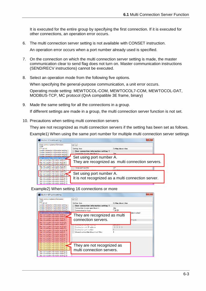
10. Precautions when setting multi connection servers
They are not recognized as multi connection servers if the setting has been set as follows.
Example1) When using the same port number for multiple multi connection server settings
Example2) When setting 16 connections or more
They are recognized as multi connection servers.
They are not recognized as multi connection servers.
Set using port number A. They are recognized as multi connection servers.
Set using port number A. It is not recognized as a multi connection server.

Multi Connection Server Function
6-4
6.1.2 Precautions When Connecting Multi Connection Servers
When connecting to a connection on which a multi connection server has been set, if the maximum number of clients connectable have been already connected, it cannot be connected to the target server port.
When connecting an additional client to the multi connection server to which the maximum number of clients have been already connected, the disconnecting operation is repeated right after the connection on the client side.
When the FP7 is the client, the master communication clear to send flag (X90 for connection 1) repeatedly turns ON and OFF.

6.2 How to Set Connections
6-5
6.2 How to Set Connections
For setting the multi connection servers, make the following settings in the user connection information setting under Built-in ET-LAN setting.
PROCEDURE
1. Set the first connection which uses the multi connection server setting.
Make this setting considering the contents of "6.1.1 Setting Conditions and Operating
Conditions".
We recommend to specify "Server connection (any destination)" for Open type
(server/client).
2. For using ten connections from the first connection, copy the contents of the first connection to ten connections.
(1) Select and right-click the source connection, and select "Copy" from the pop-up
menu.

Multi Connection Server Function
6-6
(2) Select and right-click the destination, and select "Paste" from the pop-up menu.
It is possible to select multiple destinations by dragging or using Shift or Ctrl+clicking.
(3) Select "Paste" without checking "Select Target for Automatic Serial No.".
Select "Paste" without checking the boxes for automatic serial numbers as the same
settings should be made for the multi connection server setting continuously.
3. For setting additional connections, repeat the above procedures 1 and 2.
Do not check these boxes.

Please contact ..........
■ Overseas Sales Division (He ad Office): 2431-1 Ushiyama-cho, Kasugai-shi, Aichi, 486-0901, Japan
■ Telephone: +81-568-33-7861 ■ Facsimile: +81-568-33-8591
panasonic.net/id/pidsx/global
For our sale network, please visit our website.
© Panasonic Industrial Devices SUNX Co., Ltd. 2015
151221WebDec.2015 PRINTED IN JAPAN