Flexible and Optically Transparent Polymer Embedded Nano/Micro Scale Spin Crossover Fe(II) Complex...
6
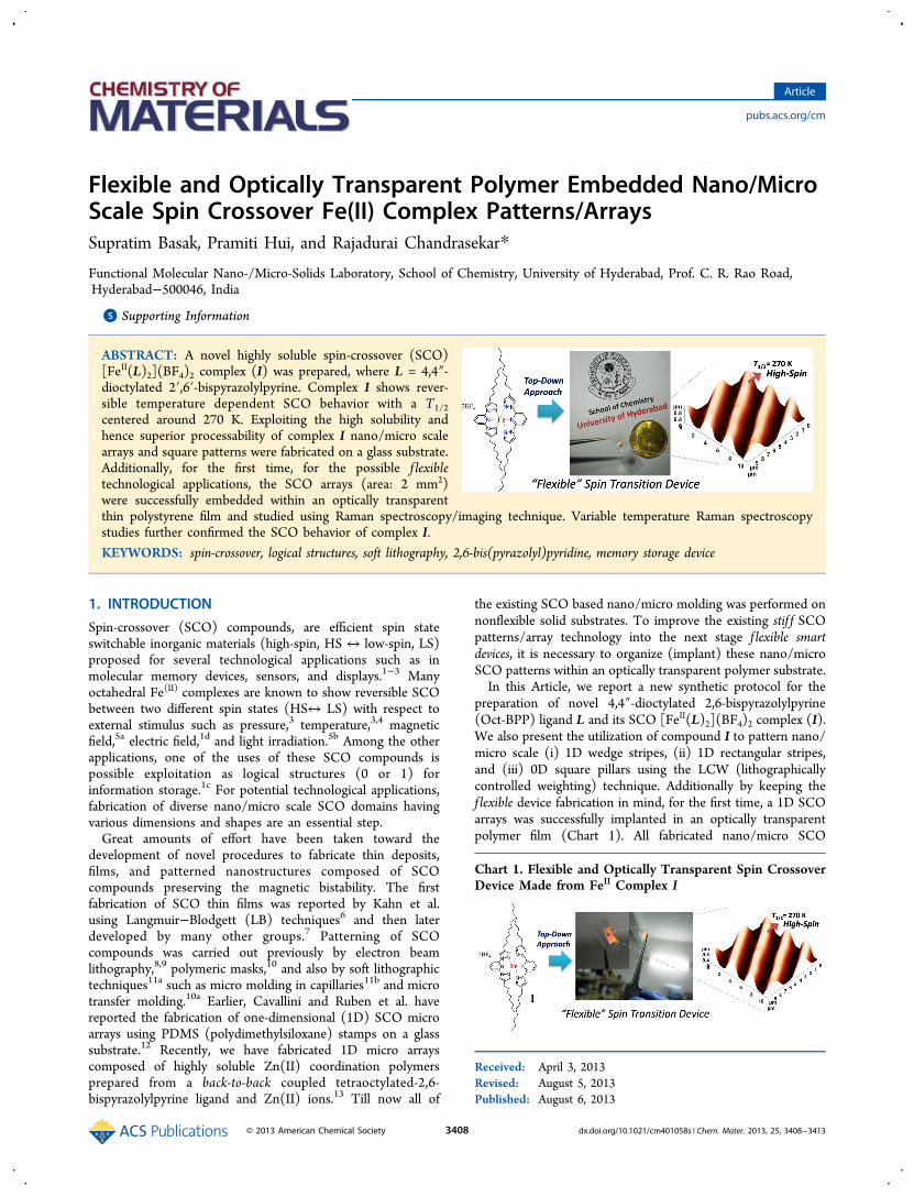
Flexible and Optically Transparent Polymer Embedded Nano/Micro Scale Spin Crossover Fe(II) Complex Patterns/Arrays Supratim Basak, Pramiti Hui, and Rajadurai Chandrasekar* Functional Molecular Nano-/Micro-Solids Laboratory, School of Chemistry, University of Hyderabad, Prof. C. R. Rao Road, Hyderabad−500046, India * S Supporting Information ABSTRACT: A novel highly soluble spin-crossover (SCO) [Fe II (L) 2 ](BF 4 ) 2 complex (I) was prepared, where L = 4,4″- dioctylated 2′,6′-bispyrazolylpyrine. Complex I shows rever- sible temperature dependent SCO behavior with a T 1/2 centered around 270 K. Exploiting the high solubility and hence superior processability of complex I nano/micro scale arrays and square patterns were fabricated on a glass substrate. Additionally, for the first time, for the possible f lexible technological applications, the SCO arrays (area: 2 mm 2 ) were successfully embedded within an optically transparent thin polystyrene film and studied using Raman spectroscopy/imaging technique. Variable temperature Raman spectroscopy studies further confirmed the SCO behavior of complex I. KEYWORDS: spin-crossover, logical structures, soft lithography, 2,6-bis(pyrazolyl)pyridine, memory storage device 1. INTRODUCTION Spin-crossover (SCO) compounds, are efficient spin state switchable inorganic materials (high-spin, HS ↔ low-spin, LS) proposed for several technological applications such as in molecular memory devices, sensors, and displays. 1−3 Many octahedral Fe (II) complexes are known to show reversible SCO between two different spin states (HS↔ LS) with respect to external stimulus such as pressure, 3 temperature, 3,4 magnetic field, 5a electric field, 1d and light irradiation. 5b Among the other applications, one of the uses of these SCO compounds is possible exploitation as logical structures (0 or 1) for information storage. 1c For potential technological applications, fabrication of diverse nano/micro scale SCO domains having various dimensions and shapes are an essential step. Great amounts of effort have been taken toward the development of novel procedures to fabricate thin deposits, films, and patterned nanostructures composed of SCO compounds preserving the magnetic bistability. The first fabrication of SCO thin films was reported by Kahn et al. using Langmuir−Blodgett (LB) techniques 6 and then later developed by many other groups. 7 Patterning of SCO compounds was carried out previously by electron beam lithography, 8,9 polymeric masks, 10 and also by soft lithographic techniques 11a such as micro molding in capillaries 11b and micro transfer molding. 10a Earlier, Cavallini and Ruben et al. have reported the fabrication of one-dimensional (1D) SCO micro arrays using PDMS (polydimethylsiloxane) stamps on a glass substrate. 12 Recently, we have fabricated 1D micro arrays composed of highly soluble Zn(II) coordination polymers prepared from a back-to-back coupled tetraoctylated-2,6- bispyrazolylpyrine ligand and Zn(II) ions. 13 Till now all of the existing SCO based nano/micro molding was performed on nonflexible solid substrates. To improve the existing stif f SCO patterns/array technology into the next stage f lexible smart devices, it is necessary to organize (implant) these nano/micro SCO patterns within an optically transparent polymer substrate. In this Article, we report a new synthetic protocol for the preparation of novel 4,4″-dioctylated 2,6-bispyrazolylpyrine (Oct-BPP) ligand L and its SCO [Fe II (L) 2 ](BF 4 ) 2 complex (I). We also present the utilization of compound I to pattern nano/ micro scale (i) 1D wedge stripes, (ii) 1D rectangular stripes, and (iii) 0D square pillars using the LCW (lithographically controlled weighting) technique. Additionally by keeping the f lexible device fabrication in mind, for the first time, a 1D SCO arrays was successfully implanted in an optically transparent polymer film (Chart 1). All fabricated nano/micro SCO Received: April 3, 2013 Revised: August 5, 2013 Published: August 6, 2013 Chart 1. Flexible and Optically Transparent Spin Crossover Device Made from Fe II Complex I Article pubs.acs.org/cm © 2013 American Chemical Society 3408 dx.doi.org/10.1021/cm401058s | Chem. Mater. 2013, 25, 3408−3413
-
Upload
independent -
Category
Documents
-
view
1 -
download
0
Transcript of Flexible and Optically Transparent Polymer Embedded Nano/Micro Scale Spin Crossover Fe(II) Complex...
Flexible and Optically Transparent Polymer Embedded Nano/MicroScale Spin Crossover Fe(II) Complex Patterns/ArraysSupratim Basak, Pramiti Hui, and Rajadurai Chandrasekar*
Functional Molecular Nano-/Micro-Solids Laboratory, School of Chemistry, University of Hyderabad, Prof. C. R. Rao Road,Hyderabad−500046, India
*S Supporting Information
ABSTRACT: A novel highly soluble spin-crossover (SCO)[FeII(L)2](BF4)2 complex (I) was prepared, where L = 4,4″-dioctylated 2′,6′-bispyrazolylpyrine. Complex I shows rever-sible temperature dependent SCO behavior with a T1/2centered around 270 K. Exploiting the high solubility andhence superior processability of complex I nano/micro scalearrays and square patterns were fabricated on a glass substrate.Additionally, for the first time, for the possible f lexibletechnological applications, the SCO arrays (area: 2 mm2)were successfully embedded within an optically transparentthin polystyrene film and studied using Raman spectroscopy/imaging technique. Variable temperature Raman spectroscopystudies further confirmed the SCO behavior of complex I.
KEYWORDS: spin-crossover, logical structures, soft lithography, 2,6-bis(pyrazolyl)pyridine, memory storage device
1. INTRODUCTION
Spin-crossover (SCO) compounds, are efficient spin stateswitchable inorganic materials (high-spin, HS ↔ low-spin, LS)proposed for several technological applications such as inmolecular memory devices, sensors, and displays.1−3 Manyoctahedral Fe(II) complexes are known to show reversible SCObetween two different spin states (HS↔ LS) with respect toexternal stimulus such as pressure,3 temperature,3,4 magneticfield,5a electric field,1d and light irradiation.5b Among the otherapplications, one of the uses of these SCO compounds ispossible exploitation as logical structures (0 or 1) forinformation storage.1c For potential technological applications,fabrication of diverse nano/micro scale SCO domains havingvarious dimensions and shapes are an essential step.Great amounts of effort have been taken toward the
development of novel procedures to fabricate thin deposits,films, and patterned nanostructures composed of SCOcompounds preserving the magnetic bistability. The firstfabrication of SCO thin films was reported by Kahn et al.using Langmuir−Blodgett (LB) techniques6 and then laterdeveloped by many other groups.7 Patterning of SCOcompounds was carried out previously by electron beamlithography,8,9 polymeric masks,10 and also by soft lithographictechniques11a such as micro molding in capillaries11b and microtransfer molding.10a Earlier, Cavallini and Ruben et al. havereported the fabrication of one-dimensional (1D) SCO microarrays using PDMS (polydimethylsiloxane) stamps on a glasssubstrate.12 Recently, we have fabricated 1D micro arrayscomposed of highly soluble Zn(II) coordination polymersprepared from a back-to-back coupled tetraoctylated-2,6-bispyrazolylpyrine ligand and Zn(II) ions.13 Till now all of
the existing SCO based nano/micro molding was performed onnonflexible solid substrates. To improve the existing stif f SCOpatterns/array technology into the next stage f lexible smartdevices, it is necessary to organize (implant) these nano/microSCO patterns within an optically transparent polymer substrate.In this Article, we report a new synthetic protocol for the
preparation of novel 4,4″-dioctylated 2,6-bispyrazolylpyrine(Oct-BPP) ligand L and its SCO [FeII(L)2](BF4)2 complex (I).We also present the utilization of compound I to pattern nano/micro scale (i) 1D wedge stripes, (ii) 1D rectangular stripes,and (iii) 0D square pillars using the LCW (lithographicallycontrolled weighting) technique. Additionally by keeping thef lexible device fabrication in mind, for the first time, a 1D SCOarrays was successfully implanted in an optically transparentpolymer film (Chart 1). All fabricated nano/micro SCO
Received: April 3, 2013Revised: August 5, 2013Published: August 6, 2013
Chart 1. Flexible and Optically Transparent Spin CrossoverDevice Made from FeII Complex I
Article
pubs.acs.org/cm
© 2013 American Chemical Society 3408 dx.doi.org/10.1021/cm401058s | Chem. Mater. 2013, 25, 3408−3413
structures were thoroughly characterized by scanning electronmicroscopy (SEM), transmission electron microscopy (TEM),atomic force microscopy (AFM), optical microscopy, andconfocal Raman imaging techniques. The SCO phenomenonwas also studied by variable temperature bulk magneticsusceptibility measurements and Raman spectroscopic studies.
2. EXPERIMENTAL SECTION2.1. Synthesis. 2,6-Bis(4-(oct-1-ynyl)-1H-pyrazol-1-yl)pyridine
(1). A Schlenk flask was charged with 2,6-bis(4-iodo-1H-pyrazol-1-yl)pyridine 2 (500 mg, 1.07 mmol) together with Pd(PPh3)2Cl2 (37.89mg, 0.053 mmol), triphenylphosphene (50 mg, 0.19 mmol) and CuI(200 mg, 0.262 mmol). Freshly distilled anhydrous triethylamine(Et3N, 20 mL) and 1,4-dioxane (10 mL) were added to it. The flaskwas carefully degassed by freeze-and-thaw cycles several times. 1-octyne (0.5 mL; d = 0.746 g/mL, 3.24 mmol) was injected into theflask under argon atmosphere, and the resulting mixture was heated to80 °C for 48 h. It was then cooled to room temperature and left forstirring for an additional 1 h. The mixture was filtered through filterpaper and washed with tetrahydrofuran (THF), and the filtrate wasevaporated to get a dark brown solid which was column chromato-graphed on silica (100−200 mesh) using initially (60:40) DCM/Hexane and finally (80:20) DCM/Hexane to get a white solid of 1.Yield 350 mg (76%). mp 86−87 °C. 1H NMR (400 MHz, CDCl3) δ:8.6 (s, 2H), 7.92−7.90 (t, 1H), 7.82−7.81 (d, 2H), 7.74 (s, 2H), 2.43−2.39 (t, 4H), 1.66−1.58 (m, 4H), 1.48−1.45 (m, 4H), 1.34 (s, 8H),0.93−0.90 (m, 6H) ppm. 13C NMR (100 MHz, CDCl3) δ: 149.5,144.6, 141.5, 129.0, 109.6, 106.6, 92.7, 70.6, 31.4, 28.7, 28.6, 22.6, 19.5,14.1 ppm. FTIR (KBr disc; ν in cm−1): 3146 (-CC-), 2926, 2848,2361, 1599, 1464, 1026, 953, 800, 656. LC-MS m/z calcd 427.27,found 428.10. ESIMS: m/z calcd 427.27, found 428.2714 [M++H].Anal. Calcd for C27H33N5: C, 75.84; H, 7.78; N, 16.38%. Found: C,75.92; H, 7.85; N, 16.27%.2,6-Bis(4-octyl-1H-pyrazol-1-yl)pyridine (L). To a degassed sol-
ution of 1 (0.3 g, 00.7 mmol) in EtOAc (60 mL) was added 10% Pd/C(0.073 g, 0.07 mmol), the mixture was stirred under H2 atmosphere(at ambient pressure), and monitored by TLC. After 1 h the mixturewas filtered through a Celite plug to remove activated Pd/C. Afterwardthe plug was washed with 100 mL of EtOAc, and the collected fractionwas concentrated in vacuum to get compound L as viscous oil. Yield0.302 g (>99%) 1H NMR (400 MHz, CDCl3) δ: 8.33 (s, 2H), 7.90−7.86 (t, 1H), 7.77−7.75 (d, 2H), 7.59 (s, 2H), 2.58−2.54 (t, 4H),1.67−1.64 (m, 4H), 1.36−1.29 (m, 20H), 0.89−0.87 (m, 6H)ppm.13C NMR (100 MHz, CDCl3) δ: 150.1, 142.5, 141.1, 124.8,124.4, 108.5, 31.9, 30.8, 29.7, 29.4, 29.3, 24.3, 22.7, 14.1 ppm. FTIR(KBr disc; ν in cm−1): 2958, 2918, 2848, 1604, 1585, 1475, 1390, 970,800, 648, 607, 536, 480, 467. LCMS analysis: m/z calcd 435.34, found436.25 (positive mode). ESIMS: m/z calcd 435.34, found 436.3403[M+ + H]. Anal. Calcd for C27H41N5: C, 74.44; H, 9.49; N, 16.08%.Found: C, 74.28; H, 9.41; N, 16.21%.[FeII(L)2](BF4)2 (I). A 100 mL flask was charged with L (80 mg, 0.183
mmol) and 10 mL of DCM was added to it. A solution of Fe(BF4)26H2O (31 mg, 0.091 mmol) in MeOH (10 mL) was added to theabove solution. The mixture was heated to reflux for 12 h at nitrogenatmosphere. After cooling, the solvent was evaporated on a rotaryevaporator in air. The residue was washed with diisopropyl ether (20mL × 1) and dried in vacuum to get a yellow color powder of I. Yield74 mg (73%). The crystals of the complex were obtained by slowevaporation from acetonitrile solution. Anal. Calcd forC54H82B2F8FeN10: C, 58.92; H, 7.51; N, 12.72%. Found: C, 58.83;H, 7.61; N, 12.52%. FTIR (KBr disc; ν in cm−1): 3118, 2958, 2927,2856, 1620, 1572, 1491, 1400, 1321, 1103 (broad, B−F), 1014, 991,796, 725, 625. M.p.: ∼80 °C.2.2. Bulk Magnetic Studies. The temperature dependent
magnetic susceptibility of complex I in the powder state was measuredon a Quantum Design vibrating sample magnetometer (VSM-SQUID)setup in the temperature range of 340↔2 K at continuous cooling (↓)and heating (↑) cycles with an applied direct current (DC) magnetic
field of 0.5 T. Heating and cooling rate of the sample was kept at a 10K interval in sweep mode.
2.3. Electron Spin Resonance Spectroscopy (EPR) Studies. X-band EPR spectra were recorded on a Bruker-ER073 spectrometerequipped with an EMX microX source. For data analysis Xenon1.1b.60 software provided by the manufacturer was used. During theliquid helium measurement the temperature was controlled by atemperature controller supplied by Oxford instruments (ITC 503S).
2.4. Method for Patterning. Micro patterning of complex I wascarried out by drop casting 20 μL of a 2 mg/mL solution of complex Iin acetonitrile (Aldrich, ≥ 99% purity) on glass substrate. Thesubstrate was cleaned by sonication for 2 min in electronic-grade water(Milli-Q-pure quality), 2 min in acetone (Aldrich chromatographyquality), and then with 2-propanol (Aldrich spectroscopic-gradequality). Before micro patterning the solution of compound I wasfiltered through a Whatman filter paper.
2.5. Stamps for Lithography..12,13 Elastomeric poly-(dimethylsiloxane) (Sylgard 184 Down Corning) stamps wereprepared by replica molding of a series of structured masters. Thecuring process was carried out for 6 h at 60 °C. Once cured, the replicawas carefully peeled off from the master and used as such for nano/micro patterning techniques. Test gratings TGQ1, TGZ3 and TGG1were purchased from NT-MDT and used as masters.
2.6. Atomic Force Microscopy (AFM). AFM imaging was carriedout on NT-MDT Model Solver Pro M microscope using a class 2Rlaser of 650 nm wavelength having maximum output of 1 mW. Allcalculations and image processing was carried out by a software NOVA1.0.26.1443 provided by the manufacturer. The images were recordedin a semicontact mode using a noncontact silicon cantilever (NSG10-DLC) tip purchased from NT-MDT, Moscow. The dimension of thetip is as follows: cantilever length = 100 (±5) μm, cantilever width 35(±5) μm, and cantilever thickness = 1.7−2.3 μm, resonate frequency =190−325 kHz, force constant = 5.5−22.5 N/m, chip size = 3.6 × 1.6 ×0.4 mm, reflective side = Au, tip height = 10−20 μm, tip curvatureradius = 1−3 nm, and aspect ratio 3:1−5:1.
2.7. Confocal Raman Micro Spectroscopy Studies. Ramanspectra of the samples were recorded on a WI-Tec confocal Ramanspectrometer equipped with a Peltier-cooled CCD detector. Using a600 grooves/mm grating BLZ = 500 nm, the accumulation time wastypically 10 s and integration time was typically 2.0000 s. Tenaccumulations was performed for acquiring a single spectrum. Forimaging the integration time was typically 2.000 s, keeping in mindthat the x or y resolution is ∼250 nm four points per line and four lineper image was taken for imaging of a 1 μm × 1 μm area. A He−Ne 633nm laser was used as an excitation source for the Raman scattering. Allmeasurements were done at ambient conditions.
2.8. Electron Microscopy Studies. Size and morphology of themicro structures were examined by using a Philips XL30 ESEMScanning Electron Microscope using a beam voltage of 20 kV. TEMmeasurement was carried out on Tecnai G2 FEI F12 instrument at anaccelerating voltage of 120 kV. Carbon coated TEM grids (200 MeshType B) were purchased from Ted Pella Inc. U.S.A.
3. RESULT AND DISCUSSION
Highly soluble ligand L was synthesized from a commerciallyavailable 2,6-dibromopyridine in four steps in good yields(Scheme 1). Conversion of 2,6-dibromopyridine into 2,6-bispyrazolylpyridine 3 was carried out as reported.14 Com-pound 3 was successfully converted to its diiodinated derivative2 as per our previously reported procedure in 74% yield.15,16
Transformation of compound 2 into 1 was achieved viaSonogashira coupling reaction conditions by using 1-octyne inEt3N/THF solvents using Pd(PPh3)2Cl2 catalyst in 78% yield.The alkyne groups in 1 were reduced using Pd/C under H2atmosphere to obtain highly soluble 2,6-dioctylated bispyr-azolylpyridine L in a quantitative 99% yield. The ligands werecharacterized by employing NMR, LC-MS, FTIR, andelemental analysis techniques. The mononuclear iron(II)
Chemistry of Materials Article
dx.doi.org/10.1021/cm401058s | Chem. Mater. 2013, 25, 3408−34133409
complex [FeII(L)2](BF4)2 (I), was synthesized from L by usingthe respective FeII salt in 2:1 DCM/MeOH solvent mixture toget a yellowish powder. Attempts to crystallize the complex I invarious solvents were unsuccessful as it formed single crystalsnot suitable for X-ray diffraction.The temperature dependent magnetic susceptibility of
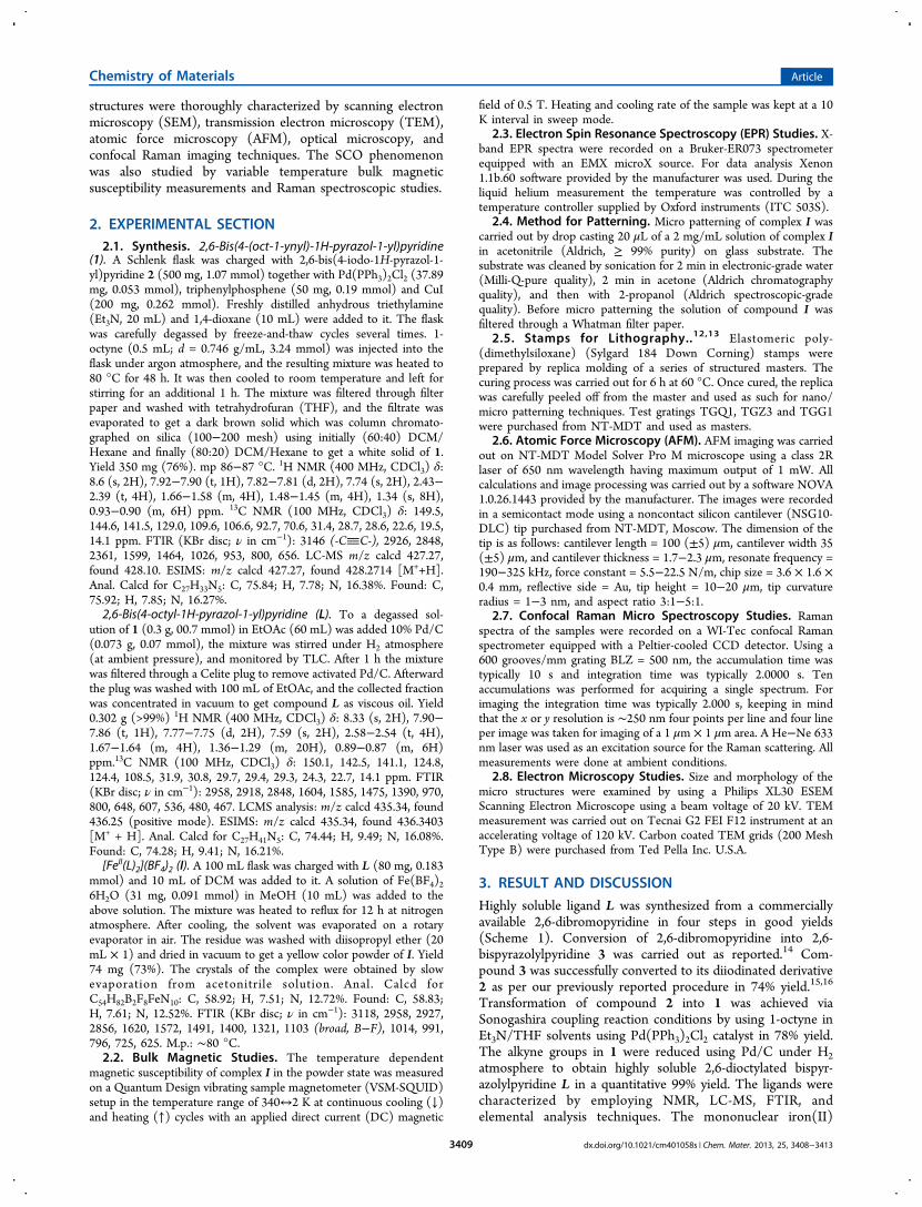
complex I showed a reversible SCO behavior at multipleheating and cooling cycles (Figure 1). The heating mode
measurement was performed only up to 340 K to avoid samplemelting. At 340 K the product of the molar magneticsusceptibility and temperature (χT) is 3.56 emu K mol−1,which is almost close to an expected value for a HS iron(II) ion(S = 2). Upon cooling the χT value decreased sharply andreached a minimum value of 1.03 emu K mol−1 down to ∼210K indicating operating SCO behavior. The calculated T1/2 valueof this regime is 270 K, which remained nearly constant forthree heating and cooling cycles. Interestingly, the SCO curvewas accompanied by a hysteresis loop (ΔT1/2). In the firstmeasurement cycle the ΔT1/2 was about 5 K, which reduced to2 K at the end of the third cycle, indicating the evaporation oftrapped solvent/moisture from the powder sample. Below 210K the χT value decreased very sluggishly and reached 0.34 emuK mol−1 at 16 K. Upon subsequent cooling the χT valuedropped down abruptly to the minimum value of 0.07 emu K
mol−1 at 2 K because of zero-field splitting of the remaining HSmolecules. Calculation of the number fraction ( f) involved inthe SCO event showed that about 70% of the moleculesundertake rather sharp SCO in the temperature range of 340K−210 K, and the remaining fractions show very sluggish SCObelow 210 K down to 16 K. The lowest value of about 0.34emu K mol−1 in the sluggish plateau indicates the presence ofparamagnetic impurities in the sample. EPR measurement ofthe sample down to 4 K confirmed the presence of HS stateFe(III) impurities by displaying characteristic peaks (Support-ing Information, Figure S10).Furthermore in Fe−N6 SCO compounds, the difference in
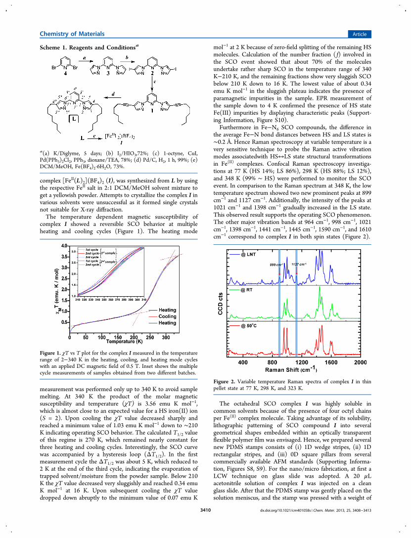
the average Fe−N bond distances between HS and LS states is∼0.2 Å. Hence Raman spectroscopy at variable temperature is avery sensitive technique to probe the Raman active vibrationmodes associatedwith HS↔LS state structural transformationsin Fe(II) complexes. Confocal Raman spectroscopy investiga-tions at 77 K (HS 14%; LS 86%), 298 K (HS 88%; LS 12%),and 348 K (99% ∼ HS) were performed to monitor the SCOevent. In comparison to the Raman spectrum at 348 K, the lowtemperature spectrum showed two new prominent peaks at 899cm−1 and 1127 cm−1. Additionally, the intensity of the peaks at1021 cm−1 and 1398 cm−1 gradually increased in the LS state.This observed result supports the operating SCO phenomenon.The other major vibration bands at 964 cm−1, 998 cm−1, 1021cm−1, 1398 cm−1, 1441 cm−1, 1445 cm−1, 1590 cm−1, and 1610cm−1 correspond to complex I in both spin states (Figure 2).
The octahedral SCO complex I was highly soluble incommon solvents because of the presence of four octyl chainsper Fe(II) complex molecule. Taking advantage of its solubility,lithographic patterning of SCO compound I into severalgeometrical shapes embedded within an optically transparentflexible polymer film was envisaged. Hence, we prepared severalnew PDMS stamps consists of (i) 1D wedge stripes, (ii) 1Drectangular stripes, and (iii) 0D square pillars from severalcommercially available AFM standards (Supporting Informa-tion, Figures S8, S9). For the nano/micro fabrication, at first aLCW technique on glass slide was adopted. A 20 μLacetonitrile solution of complex I was injected on a cleanglass slide. After that the PDMS stamp was gently placed on thesolution meniscus, and the stamp was pressed with a weight of
Scheme 1. Reagents and Conditionsa
a(a) K/Diglyme, 5 days; (b) I2/HIO3,72%; (c) 1-octyne, CuI,Pd(PPh3)2Cl2, PPh3, dioxane/TEA, 78%; (d) Pd/C, H2, 1 h, 99%; (e)DCM/MeOH, Fe(BF4)2·6H2O, 73%.
Figure 1. χT vs T plot for the complex I measured in the temperaturerange of 2−340 K in the heating, cooling, and heating mode cycleswith an applied DC magnetic field of 0.5 T. Inset shows the multiplecycle measurements of samples obtained from two different batches.
Figure 2. Variable temperature Raman spectra of complex I in thinpellet state at 77 K, 298 K, and 323 K.
Chemistry of Materials Article
dx.doi.org/10.1021/cm401058s | Chem. Mater. 2013, 25, 3408−34133410
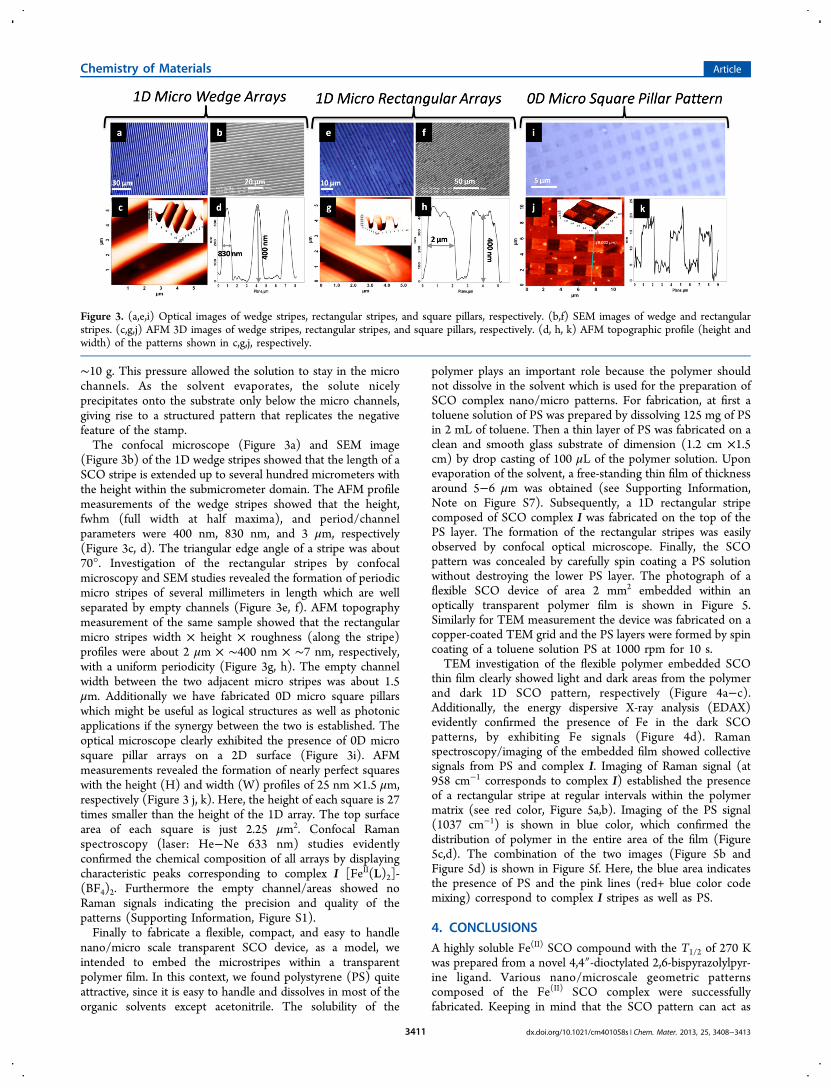
∼10 g. This pressure allowed the solution to stay in the microchannels. As the solvent evaporates, the solute nicelyprecipitates onto the substrate only below the micro channels,giving rise to a structured pattern that replicates the negativefeature of the stamp.The confocal microscope (Figure 3a) and SEM image
(Figure 3b) of the 1D wedge stripes showed that the length of aSCO stripe is extended up to several hundred micrometers withthe height within the submicrometer domain. The AFM profilemeasurements of the wedge stripes showed that the height,fwhm (full width at half maxima), and period/channelparameters were 400 nm, 830 nm, and 3 μm, respectively(Figure 3c, d). The triangular edge angle of a stripe was about70°. Investigation of the rectangular stripes by confocalmicroscopy and SEM studies revealed the formation of periodicmicro stripes of several millimeters in length which are wellseparated by empty channels (Figure 3e, f). AFM topographymeasurement of the same sample showed that the rectangularmicro stripes width × height × roughness (along the stripe)profiles were about 2 μm × ∼400 nm × ∼7 nm, respectively,with a uniform periodicity (Figure 3g, h). The empty channelwidth between the two adjacent micro stripes was about 1.5μm. Additionally we have fabricated 0D micro square pillarswhich might be useful as logical structures as well as photonicapplications if the synergy between the two is established. Theoptical microscope clearly exhibited the presence of 0D microsquare pillar arrays on a 2D surface (Figure 3i). AFMmeasurements revealed the formation of nearly perfect squareswith the height (H) and width (W) profiles of 25 nm ×1.5 μm,respectively (Figure 3 j, k). Here, the height of each square is 27times smaller than the height of the 1D array. The top surfacearea of each square is just 2.25 μm2. Confocal Ramanspectroscopy (laser: He−Ne 633 nm) studies evidentlyconfirmed the chemical composition of all arrays by displayingcharacteristic peaks corresponding to complex I [FeII(L)2]-(BF4)2. Furthermore the empty channel/areas showed noRaman signals indicating the precision and quality of thepatterns (Supporting Information, Figure S1).Finally to fabricate a flexible, compact, and easy to handle
nano/micro scale transparent SCO device, as a model, weintended to embed the microstripes within a transparentpolymer film. In this context, we found polystyrene (PS) quiteattractive, since it is easy to handle and dissolves in most of theorganic solvents except acetonitrile. The solubility of the
polymer plays an important role because the polymer shouldnot dissolve in the solvent which is used for the preparation ofSCO complex nano/micro patterns. For fabrication, at first atoluene solution of PS was prepared by dissolving 125 mg of PSin 2 mL of toluene. Then a thin layer of PS was fabricated on aclean and smooth glass substrate of dimension (1.2 cm ×1.5cm) by drop casting of 100 μL of the polymer solution. Uponevaporation of the solvent, a free-standing thin film of thicknessaround 5−6 μm was obtained (see Supporting Information,Note on Figure S7). Subsequently, a 1D rectangular stripecomposed of SCO complex I was fabricated on the top of thePS layer. The formation of the rectangular stripes was easilyobserved by confocal optical microscope. Finally, the SCOpattern was concealed by carefully spin coating a PS solutionwithout destroying the lower PS layer. The photograph of aflexible SCO device of area 2 mm2 embedded within anoptically transparent polymer film is shown in Figure 5.Similarly for TEM measurement the device was fabricated on acopper-coated TEM grid and the PS layers were formed by spincoating of a toluene solution PS at 1000 rpm for 10 s.TEM investigation of the flexible polymer embedded SCO
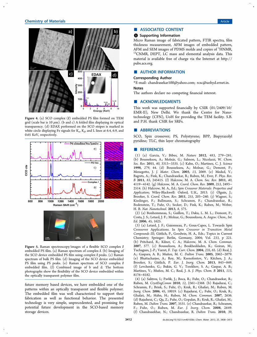
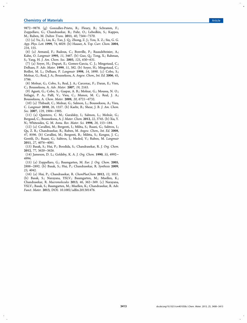
thin film clearly showed light and dark areas from the polymerand dark 1D SCO pattern, respectively (Figure 4a−c).Additionally, the energy dispersive X-ray analysis (EDAX)evidently confirmed the presence of Fe in the dark SCOpatterns, by exhibiting Fe signals (Figure 4d). Ramanspectroscopy/imaging of the embedded film showed collectivesignals from PS and complex I. Imaging of Raman signal (at958 cm−1 corresponds to complex I) established the presenceof a rectangular stripe at regular intervals within the polymermatrix (see red color, Figure 5a,b). Imaging of the PS signal(1037 cm−1) is shown in blue color, which confirmed thedistribution of polymer in the entire area of the film (Figure5c,d). The combination of the two images (Figure 5b andFigure 5d) is shown in Figure 5f. Here, the blue area indicatesthe presence of PS and the pink lines (red+ blue color codemixing) correspond to complex I stripes as well as PS.
4. CONCLUSIONSA highly soluble Fe(II) SCO compound with the T1/2 of 270 Kwas prepared from a novel 4,4″-dioctylated 2,6-bispyrazolylpyr-ine ligand. Various nano/microscale geometric patternscomposed of the Fe(II) SCO complex were successfullyfabricated. Keeping in mind that the SCO pattern can act as
Figure 3. (a,e,i) Optical images of wedge stripes, rectangular stripes, and square pillars, respectively. (b,f) SEM images of wedge and rectangularstripes. (c,g,j) AFM 3D images of wedge stripes, rectangular stripes, and square pillars, respectively. (d, h, k) AFM topographic profile (height andwidth) of the patterns shown in c,g,j, respectively.
Chemistry of Materials Article
dx.doi.org/10.1021/cm401058s | Chem. Mater. 2013, 25, 3408−34133411
future memory based devices, we have embedded one of thepatterns within an optically transparent and flexible polymer.The embedded film was well characterized to support theirfabrication as well as functional behavior. The presentedtechnology is very simple, unprecedented, and promising forpotential future development in the SCO-based memorystorage devices.
■ ASSOCIATED CONTENT*S Supporting InformationMicro Raman image of fabricated pattern, FTIR spectra, filmthickness measurement, AFM images of embedded pattern,AFM and SEM images of PDMS molds and copies of 1HNMR,13CNMR, DEPT, LC mass and elemental analysis data. Thismaterial is available free of charge via the Internet at http://pubs.acs.org.
■ AUTHOR INFORMATIONCorresponding Author*E-mail: [email protected]; [email protected] authors declare no competing financial interest.
■ ACKNOWLEDGMENTSThis work was supported financially by CSIR (01/2409/10/EMR-II), New Delhi. We thank the Centre for Nano-technology (CFN), UoH for providing the TEM facility. S.B.and P.H. thank CSIR for SRFs.
■ ABBREVIATIONSSCO, Spin crossover; PS, Polystyrene; BPP, Bispyrazolylpyridine; TLC, thin layer chromatography
■ REFERENCES(1) (a) Garcia, V.; Bibes, M. Nature 2012, 483, 279−281.(b) Bousseksou, A.; Molnar, G.; Salmon, L.; Nicolazzi, W. Chem.Soc. Rev. 2011, 40, 3313−3335. (c) Kahn, O.; Martinez, C. J. Science1998, 279, 44. (d) Bousseksou, A.; Molnar, G.; Demont, P.;Menegotto, J. J. Mater. Chem. 2003, 13, 2069. (e) Meded, V.;Bagrets, A.; Fink, K.; Chandrasekar, R.; Ruben, M.; Ever, F. Phys. Rev.B 2011, 83, 245415. (f) Halcrow, M. A. Chem. Soc. Rev. 2011, 40,4119−4142. (g) Halcrow, M. A. Coord. Chem. Rev. 2009, 253, 2493−2514. (h) Halcrow, M. A., Ed.; Spin Crossover Materials: Properties andApplication; Wiley-Blackwell: Oxford, U.K., 2013. (i) Olguín, J.;Brooker, S. Coord. Chem. Rev. 2011, 255, 203−240. (j) Wagner, S.;Kisslinger, F.; Ballmann, S.; Schramm, F.; Chandrasekar, R.;Bodenstein, T.; Fuhr, O.; Secker, D.; Fink, K.; Ruben, M.; Weber,H. B. Nat. Nanotechnol. 2013, 8, 575.(2) (a) Bonhommeau, S.; Guillon, T.; Daku, L. M. L.; Demont, P.;Costa, J. S.; Letard, J. F.; Molnar, G.; Bousseksou, A. Angew. Chem., Int.Ed. 2006, 45, 1625.(3) (a) Letard, J. F.; Guionneau, P.; Goux-Capes, L. Towards SpinCrossover Applications. In Spin Crossover in Transition MetalCompounds III; Gutlich, P., Goodwin, H. A., Eds.; Topics in CurrentChemistry; Springer: Berlin, Germany, 2004; Vol. 233, p 221.(b) Pritchard, R.; Kilner, C. A.; Halcrow, M. A. Chem. Commun.2007, 577. (c) Bousseksou, A.; Boukheddaden, K.; Goiran, M.;Tuchagues, J.-P.; Varret, F. Top. Curr. Chem. 2004, 235, 65. (d) Real, J.A.; Gaspara, A. B.; Munoz, M. C. Dalton Trans. 2005, 2062−2079.(e) Bhattacharjee, A.; Roy, M.; Ksenofontov, V.; Kitchen, J. A.;Brooker, S.; Gutlich, P. Eur. J. Inorg. Chem. 2013, 843−849.(f) Levchenko, G.; Bukin, G. V.; Terekhov, S. A.; Gaspar, A. B.;Martínez, V.; Munoz, M. C.; Real, J. A. J. Phys. Chem. B 2011, 115,8176−8182.(4) (a) Salitros, I.; Pavlik, J.; Boca, R.; Fuhr, O.; Chandrasekar, R.;Ruben, M. CrystEngComm 2010, 12, 2361−2368. (b) Rajadurai, C.;Schramm, F.; Brink, S.; Fuhr, O.; Kruk, R.; Ghafari, M.; Ruben, M.Inorg. Chem. 2006, 45, 10019. (c) Rajadurai, C.; Fuhr, O.; Kruk, R.;Ghafari, M.; Hahn, H.; Ruben, M. Chem. Commun. 2007, 2636.(d) Rajadurai, C.; Qu, Z.; Fuhr, O.; Gopalan, B.; Kruk, R.; Ghafari, M.;Ruben, M. Dalton Trans. 2007, 3531. (e) Chandrasekar, R.; Schramm,F.; Fuhr, O.; Ruben, M. Eur. J. Inorg. Chem. 2008, 2649.(f) Chandrasekhar, N.; Chandrasekar, R. Dalton Trans. 2010, 39,
Figure 4. (a) SCO complex (I) embedded PS film formed on TEMgrid (scale bar is 10 μm). (b and c) A folded film displaying its opticaltransparency. (d) EDAX performed on the SCO stripes is marked inwhite circle displaying Fe signals for Kα, Kβ, and L lines at 6.4, 6.9, and0.65 KeV, respectively.
Figure 5. Raman spectroscopy/images of a flexible SCO complex Iembedded PS film. (a) Raman spectrum of complex I. (b) Imaging ofthe SCO device embedded PS film using complex I peaks. (c) Ramanspectrum of bulk PS film. (d) Imaging of the SCO device embeddedPS film using PS peaks. (e) Raman spectrum of SCO complex Iembedded film. (f) Combined image of b and d. The bottomphotographs show the flexibility of the SCO device embedded withinthe optically transparent polymer film.
Chemistry of Materials Article
dx.doi.org/10.1021/cm401058s | Chem. Mater. 2013, 25, 3408−34133412
9872−9878. (g) Gonzallez-Prieto, R.; Fleury, B.; Schramm, F.;Zoppellaro, G.; Chandrasekar, R.; Fuhr, O.; Lebedkin, S.; Kappes,M.; Ruben, M. Dalton Trans. 2011, 40, 7564−7570.(5) (a) Yu, Z.; Liu, K.; Tao, J. Q.; Zhong, Z. J.; You, X. Z.; Siu, G. G.App. Phys. Lett. 1999, 74, 4029. (b) Hauser, A. Top. Curr. Chem. 2004,234, 155.(6) (a) Armand, F.; Badoux, C.; Bonville, P.; Ruaudelteixier, A.;Kahn, O. Langmuir 1995, 11, 3467. (b) Guo, Q.; Teng, X.; Rahman,S.; Yang, H. J. Am. Chem. Soc. 2003, 125, 630−631.(7) (a) Soyer, H.; Dupart, E.; Gomez-Garcia, C. J.; Mingotaud, C.;Delhaes, P. Adv. Mater. 1999, 11, 382. (b) Soyer, H.; Mingotaud, C.;Boillot, M. L.; Delhaes, P. Langmuir 1998, 14, 5890. (c) Cobo, S.;Molnar, G.; Real, J. A.; Bousseksou, A. Angew. Chem., Int. Ed. 2006, 45,5786.(8) Molnar, G.; Cobo, S.; Real, J. A.; Carcenac, F.; Daran, E.; Vien,C.; Bousseksou, A. Adv. Mater. 2007, 19, 2163.(9) Agusti, G.; Cobo, S.; Gaspar, A. B.; Molnar, G.; Moussa, N. O.;Szilagyi, P. A.; Palfi, V.; Vieu, C.; Munoz, M. C.; Real, J. A.;Bousseksou, A. Chem. Mater. 2008, 20, 6721−6732.(10) (a) Thibault, C.; Molnar, G.; Salmon, L.; Bousseksou, A.; Vieu,C. Langmuir 2010, 26, 1557. (b) Kaehr, B.; Shear, J. B. J. Am. Chem.Soc. 2007, 129, 1904−1905.(11) (a) Quintero, C. M.; Guralskiy, I.; Salmon, L.; Molnar, G.;Bergaud, C.; Bousseksou, A. J. Mater. Chem. 2012, 22, 3745. (b) Xia, Y.N.; Whitesides, G. M. Annu. Rev. Mater. Sci. 1998, 28, 153−184.(12) (a) Cavallini, M.; Bergenti, I.; Milita, S.; Ruani, G.; Salitros, I.;Qu, Z. R.; Chandrasekar, R.; Ruben, M. Angew. Chem., Int. Ed. 2008,47, 8596. (b) Cavallini, M.; Bergenti, B.; Militta, S.; Kengne, J. C.;Gentili, D.; Ruani, G.; Salitros, I.; Meded, V.; Ruben, M. Langmuir2011, 27, 4076−4081.(13) Basak, S.; Hui, P.; Boodida, S.; Chandrasekar, R. J. Org. Chem.2012, 77, 3620−3626.(14) Jameson, D. L.; Goldsby, K. A. J. Org. Chem. 1990, 55, 4992−4994.(15) (a) Zoppellaro, G.; Baumgarten, M. Eur. J. Org. Chem. 2005,2888−2892. (b) Basak, S.; Hui, P.; Chandrasekar, R. Synthesis 2009,23, 4042.(16) (a) Hui, P.; Chandrasekar, R. ChemPlusChem 2012, 12, 1051.(b) Basak, S.; Narayana, YSLV.; Baumgarten, M.; Muellen, K.;Chandrasekar, R. Macromolecules 2013, 46, 362−369. (c) Narayana,YSLV.; Basak, S.; Baumgarten, M.; Muellen, K.; Chandrasekar, R. Adv.Funct. Mater. 2013, DOI: 10.1002/adfm.201301476.
Chemistry of Materials Article
dx.doi.org/10.1021/cm401058s | Chem. Mater. 2013, 25, 3408−34133413