The effect of Fe‐acceptor doping on the electrical properties of ...
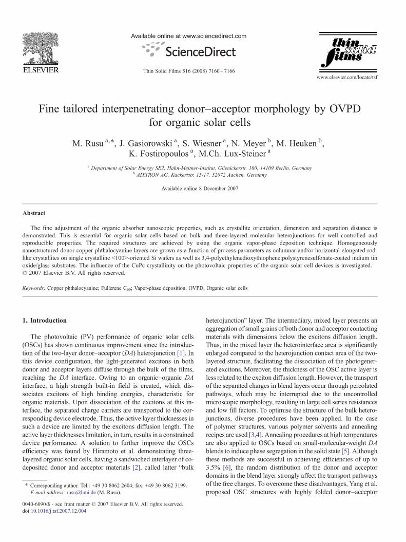
Available online at www.sciencedirect.com
008) 7160–7166www.elsevier.com/locate/tsf
Thin Solid Films 516 (2
Fine tailored interpenetrating donor–acceptor morphology by OVPDfor organic solar cells
M. Rusu a,⁎, J. Gasiorowski a, S. Wiesner a, N. Meyer b, M. Heuken b,K. Fostiropoulos a, M.Ch. Lux-Steiner a
a Department of Solar Energy SE2, Hahn-Meitner-Institut, Glienickerstr. 100, 14109 Berlin, Germanyb AIXTRON AG, Kackertstr. 15-17, 52072 Aachen, Germany
Available online 8 December 2007
Abstract
The fine adjustment of the organic absorber nanoscopic properties, such as crystallite orientation, dimension and separation distance isdemonstrated. This is essential for organic solar cells based on bulk and three-layered molecular heterojunctions for well controlled andreproducible properties. The required structures are achieved by using the organic vapor-phase deposition technique. Homogeneouslynanostructured donor copper phthalocyanine layers are grown as a function of process parameters as columnar and/or horizontal elongated-rod-like crystallites on single crystalline b100N-oriented Si wafers as well as 3,4-polyethylenedioxythiophene:polystyrenesulfonate-coated indium tinoxide/glass substrates. The influence of the CuPc crystallinity on the photovoltaic properties of the organic solar cell devices is investigated.© 2007 Elsevier B.V. All rights reserved.
Keywords: Copper phthalocyanine; Fullerene C60; Vapor-phase deposition; OVPD; Organic solar cells
1. Introduction
The photovoltaic (PV) performance of organic solar cells(OSCs) has shown continuous improvement since the introduc-tion of the two-layer donor–acceptor (DA) heterojunction [1]. Inthis device configuration, the light-generated excitons in bothdonor and acceptor layers diffuse through the bulk of the films,reaching the DA interface. Owing to an organic–organic DAinterface, a high strength built-in field is created, which dis-sociates excitons of high binding energies, characteristic fororganic materials. Upon dissociation of the excitons at this in-terface, the separated charge carriers are transported to the cor-responding device electrode. Thus, the active layer thicknesses insuch a device are limited by the excitons diffusion length. Theactive layer thicknesses limitation, in turn, results in a constraineddevice performance. A solution to further improve the OSCsefficiency was found by Hiramoto et al. demonstrating three-layered organic solar cells, having a sandwiched interlayer of co-deposited donor and acceptor materials [2], called latter “bulk
⁎ Corresponding author. Tel.: +49 30 8062 2604; fax: +49 30 8062 3199.E-mail address: [email protected] (M. Rusu).
0040-6090/$ - see front matter © 2007 Elsevier B.V. All rights reserved.doi:10.1016/j.tsf.2007.12.004
heterojunction” layer. The intermediary, mixed layer presents anaggregation of small grains of both donor and acceptor contactingmaterials with dimensions below the excitons diffusion length.Thus, in the mixed layer the heterointerface area is significantlyenlarged compared to the heterojunction contact area of the two-layered structure, facilitating the dissociation of the photogener-ated excitons. Moreover, the thickness of the OSC active layer isless related to the exciton diffusion length. However, the transportof the separated charges in blend layers occur through percolatedpathways, which may be interrupted due to the uncontrolledmicroscopic morphology, resulting in large cell series resistancesand low fill factors. To optimise the structure of the bulk hetero-junctions, diverse procedures have been applied. In the caseof polymer structures, various polymer solvents and annealingrecipes are used [3,4]. Annealing procedures at high temperaturesare also applied to OSCs based on small-molecular-weight DAblends to induce phase segregation in the solid state [5]. Althoughthese methods are successful in achieving efficiencies of up to3.5% [6], the random distribution of the donor and acceptordomains in the blend layer strongly affect the transport pathwaysof the free charges. To overcome these disadvantages, Yang et al.proposed OSC structures with highly folded donor–acceptor

7161M. Rusu et al. / Thin Solid Films 516 (2008) 7160–7166
interface, resulting from the morphology of the primarilydeposited donor layer, achieving device efficiencies of 5.0%[7]. Usami et al. proposes to utilise the growth of island crystals tofurther increase the bulk heterojunction structure [8]. First resultshave been demonstrated on organic layers grown on high-qualityhydrogen terminated Si(111) substrates.
From the above discussed it follows that further increase ofthe OSCs conversion efficiency is related to the controlledformation of single crystalline layers with pre-required dimen-sions of the crystallites height and width as well as of thedistances between them for one of the organic materials in thebulk heterojunction layer on an appropriate substrate. Anotherorganic material is deposited subsequently on top of the firstlayer to form an interpenetrating D:A structure. In such struc-tures, the transport pathways of separated carriers to the contactsbecome guaranteed; the enhanced material crystallinity leads toincreased carrier mobility, thus improving charge-carrier trans-port. Fulfilling this requirements, preparation of OSCs withthicker active layers and thus with an enhanced absorptionbecomes possible.
In this work, we study the growth of the copper phthalocya-nine, CuPc, donor material by organic vapor-phase deposition(OVPD) on b100N-oriented Si wafers as well as 3,4-poly-ethylenedioxythiophene:polystyrenesulfonate (PEDOT:PSS)-coated indium tin oxide (ITO) on glass substrates, which arewidely used for the preparation of organic solar cells. We dem-onstrate formation of high-quality single crystalline CuPc layersgrown on both types of substrates. We show that the shape of theCuPc crystallites can be fine tuned from columnar- to elongatedhorizontal rods-like ones. Solar cells with both co-deposited,mixed D:A layers and PV cells with controlled nanostructureddonor-CuPc layers are studied.
2. Experimental
A commercial OVPD® system (Aixtron) [9] is employed forthe deposition of materials used for preparation of PV cells [10].The organic materials used in this work—CuPc and the fullereneC60, are volatilized in special source containers in the presence ofN2 inert gas that transforms the pickup of material into anequilibrium process [11]. The CuPc source temperature (Tsource) ismaintained constant at 411 °C, while a constant Tsource=422 °C isset for the C60 container. N2 is also used as a carrier gas fortransportingmaterials into the deposition chamber. The carrier gasquantities through each source, Qsource, are externally controlledby mass-flow controllers. The chamber pressure Pchamber is ac-curately controlled and can be precisely varied between 10−1 and103 mbar. The materials deposition rates at a certain substratetemperature (Tsubstrate) and chamber pressure are preciselycontrolled by adjusting Qsource. The OVPD chamber is directlyattached to a high vacuum chamber (base pressure ~10−7 mbar)designed for deposition of solar cells' metallic contacts as well asfor charging/discharging substrates/complete solar cell devicesinto/from the OVPD system. The samples are transferred to/fromthe OVPD and vacuum chamber systems through a N2-filledglove-box. Further details about the OVPD setup can be foundelsewhere [9,10].
Silicon b100N-oriented wafers and PEDOT:PSS-coated ITO/glass substrates were used for calibration runs and preparationof solar cells, respectively. Standard wet chemistry was used toprepare the Si (native oxide only) and ITO substrates prior tosubsequent depositions. The substrates were first degreasedwith organic solvents and detergents in an ultrasonic bath,rinsed then in de-ionised water and dried in a nitrogen flux.
The layers thicknesses on Si wafers were determined by usingoptical measurements and microscopy observations. Opticalmeasurements included spectrometry as well as ellipsometerycharacterisation techniques. A Filmetrics F20 apparatus with atwo-source illumination system (xenon and halogen lamps)Hamamatsu L7893 was used for the layers thickness determina-tion by fitting the reflectance spectra. The ellipsometric measure-ments were performed with a Plasmos SD2302 device on anincident light wavelength of λ=1520 nm, varying the incidentangle between 65° and 75°. The layer parameters were calculatedby fitting the polarized ellipsometric spectra. The cross-sectionand surface morphology of the organic layers were investigatedby scanning electron microscopy (SEM), using a commercialGemini LEO 1530 microscope. The crystal structure of theorganic layers and their preferential orientation was determinedby X-ray diffraction (XRD) with a Bruker D8 diffractometer inthe θ–2θ geometry and continuous sample rotation.
Organic solar cell devices were fabricated on glass substratescommercially pre-coated with a transparent, conducting ITOlayer with a sheet resistance of 5 Ω/sq. After solvent cleaning,the ITO/glass substrates were spin-coated by a PEDOT:PSSlayer. The CuPc donor and the C60 acceptor materials weredeposited by the OVPD technique, while the Mg/Ag backcontacts were deposited in the high vacuum chamber withoutexposing the corresponding absorber/metal interface to air.
The OSCs PV parameters – power conversion efficiency(Eff), fill factor (FF), open circuit voltage (Voc), short-circuitcurrent density (Jsc) – are determined from J–V measure-ments performed under standard test conditions (AM1.5;100 mW/cm2; 25 °C).
3. Results
3.1. C60 films on Si substrates
C60 layers deposited on Si b100N show an island-like growth[10]. This growth mechanism is characteristic for all the filmsdeposited in the temperature range investigated 96–187 °C. TheX-ray diffraction patterns of C60 films on Si substrates exhibitan almost amorphous structure (not shown). Only a weak andbroad 002 peak corresponding to the C60 hexagonal close-packed (hcp) structure is observed in the X-ray diffractionscans. The C60 deposition rate is controlled by the N2 fluxthrough C60 container. Further details about C60 morphologyand structural properties can be found in Ref. [10].
3.2. CuPc films on Si substrates
Fig. 1a–f shows the SEM images of the morphologicalevolution of the OVPD-grown CuPc layers on Si b100N-

Fig. 1. Cross-section (60° view angle) and top view (insets) SEM images of CuPc layers deposited on Si b100N-oriented wafers at substrate temperatures anddeposition pressures of (a) 96 °C and 2.5 mbar, (b) 111 °C and 1.5 mbar, (c) 120 °C and 1.2 mbar, (d) 131 °C and 0.9 mbar, (e) 151 °C and 0.6 mbar, and (f) 187 °C and0.3 mbar, respectively and Tsource=411 °C, Qsource=400 sccm, and Qtotal=1050 sccm.
Fig. 2. X-ray CuKα1,2 diffraction patterns of CuPc layers on the surface of Sib100N-oriented wafers in Fig. 1(a–f). The peaks corresponding to the α-phaseCuPc are identified according to Ref. [12].
7162 M. Rusu et al. / Thin Solid Films 516 (2008) 7160–7166
oriented substrates (native oxide only) as a function of substratetemperature that varies between 96 °C and 187 °C. To achievean optimal film homogeneity, the chamber pressure wasadjusted at 0.3 mbar for layers grown at high substrate tem-perature, 187 °C, and increased up to 2.5 mbar for the filmsdeposited at low temperatures, 96 °C. The source flow rate wasset to 400 sccm (sccm denotes cubic centimetre per minute).The deposition time of 30 min was the same for all samples.CuPc films grown at low temperatures and those grown at hightemperatures show dramatically different morphologies andstructures. At Tsubstrate=96 °C the films in Fig. 1a have fine-fibril structures. With the substrate temperature increase upto 111 °C a decrease in the film thickness and aggregation ofvertically arranged small grains is observed (Fig. 1b). Furtherincrease of the substrate temperature results in coalescence ofthe small grains (Fig. 1c). As a result, a clear columnar growthis observed in Fig. 1d–e in the substrate temperature range of131–150 °C. However, already at these temperatures, besidecolumnar-like structures, formation of elongated-rod-like crystal-lites is observed. Their surface density, which increases with thetemperature (compare Fig. 1d,e), is caused by the coalescence ofthe neighbour columnar crystallites. At Tsubstrate=187 °C thesubstrate is completely and homogeneously covered by layersconsisting of only elongated rods-like crystallites. Thus, byadjusting the deposition temperature, nanostructured CuPc layerscan be achieved. Moreover, the crystallites dimensions as wellas the distances between them can be fine controlled. It has tobe mentioned that the width of both columnar and verticallyelongated rods-like CuPc crystallites in Fig. 1e–f is of about 20 to50 nm. In addition, the distances between CuPc nanocrystallitesare of up to 20 nm in columnar-structured layers and basically lessthan 50 nm for rod-like-structured films.
The X-ray diffraction patterns of the layers in Fig. 1 areshown in Fig. 2. The pattern in Fig. 2a of the film in Fig. 1ashows the substrate related Si 200 peak only. No characteristic
features of any of the CuPc polymorphs are observed, whichindicates that the dimensions of the CuPc “fibres” are not largeenough to produce an effective X-ray diffraction. When thesubstrate temperature increases up to 111 °C, Fig. 2b, a broadpeak at 2θ=6.83° evolves. For substrate temperatures in therange of 120–131 °C, the XRD patterns in Fig. 2c–d showcharacteristic features of the α-polymorph of Cu-phthalocya-nine, which posses a monoclinic structure [12]. The peaks thatcorrespond to X-ray diffractions from planes (111), (112) and(312) vanish at Tsubstrate=151 °C (Fig. 2e). Only (h00) dif-fraction peaks are present in the XRD patterns measured onCuPc layers at these and higher temperatures. The sharpness ofall the (h00) peaks increases at elevated substrate temperatures.Thus, it can be concluded that at high temperatures the a axis ofthe monoclinic unit cell is perpendicular to the substrate plane.
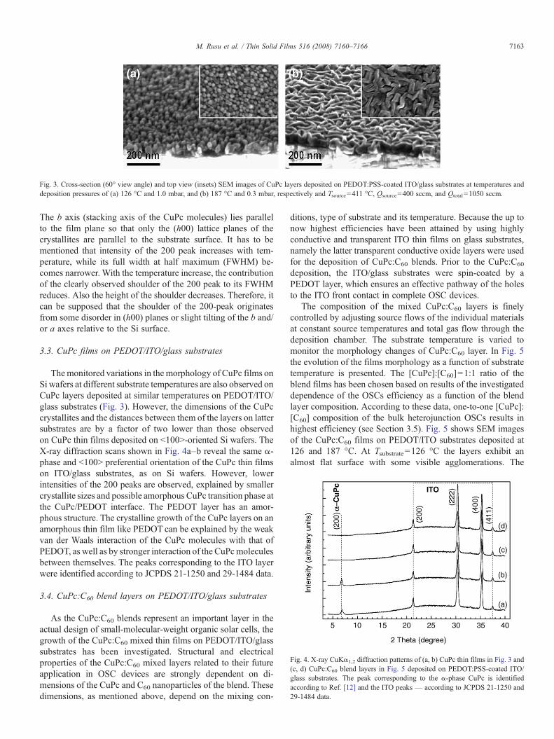
Fig. 3. Cross-section (60° view angle) and top view (insets) SEM images of CuPc layers deposited on PEDOT:PSS-coated ITO/glass substrates at temperatures anddeposition pressures of (a) 126 °C and 1.0 mbar, and (b) 187 °C and 0.3 mbar, respectively and Tsource=411 °C, Qsource=400 sccm, and Qtotal=1050 sccm.
Fig. 4. X-ray CuKα1,2 diffraction patterns of (a, b) CuPc thin films in Fig. 3 and(c, d) CuPc:C60 blend layers in Fig. 5 deposited on PEDOT:PSS-coated ITO/glass substrates. The peak corresponding to the α-phase CuPc is identifiedaccording to Ref. [12] and the ITO peaks — according to JCPDS 21-1250 and29-1484 data.
7163M. Rusu et al. / Thin Solid Films 516 (2008) 7160–7166
The b axis (stacking axis of the CuPc molecules) lies parallelto the film plane so that only the (h00) lattice planes of thecrystallites are parallel to the substrate surface. It has to bementioned that intensity of the 200 peak increases with tem-perature, while its full width at half maximum (FWHM) be-comes narrower. With the temperature increase, the contributionof the clearly observed shoulder of the 200 peak to its FWHMreduces. Also the height of the shoulder decreases. Therefore, itcan be supposed that the shoulder of the 200-peak originatesfrom some disorder in (h00) planes or slight tilting of the b and/or a axes relative to the Si surface.
3.3. CuPc films on PEDOT/ITO/glass substrates
Themonitored variations in the morphology of CuPc films onSi wafers at different substrate temperatures are also observed onCuPc layers deposited at similar temperatures on PEDOT/ITO/glass substrates (Fig. 3). However, the dimensions of the CuPccrystallites and the distances between them of the layers on lattersubstrates are by a factor of two lower than those observedon CuPc thin films deposited on b100N-oriented Si wafers. TheX-ray diffraction scans shown in Fig. 4a–b reveal the same α-phase and b100N preferential orientation of the CuPc thin filmson ITO/glass substrates, as on Si wafers. However, lowerintensities of the 200 peaks are observed, explained by smallercrystallite sizes and possible amorphous CuPc transition phase atthe CuPc/PEDOT interface. The PEDOT layer has an amor-phous structure. The crystalline growth of the CuPc layers on anamorphous thin film like PEDOT can be explained by the weakvan der Waals interaction of the CuPc molecules with that ofPEDOT, as well as by stronger interaction of the CuPcmoleculesbetween themselves. The peaks corresponding to the ITO layerwere identified according to JCPDS 21-1250 and 29-1484 data.
3.4. CuPc:C60 blend layers on PEDOT/ITO/glass substrates
As the CuPc:C60 blends represent an important layer in theactual design of small-molecular-weight organic solar cells, thegrowth of the CuPc:C60 mixed thin films on PEDOT/ITO/glasssubstrates has been investigated. Structural and electricalproperties of the CuPc:C60 mixed layers related to their futureapplication in OSC devices are strongly dependent on di-mensions of the CuPc and C60 nanoparticles of the blend. Thesedimensions, as mentioned above, depend on the mixing con-
ditions, type of substrate and its temperature. Because the up tonow highest efficiencies have been attained by using highlyconductive and transparent ITO thin films on glass substrates,namely the latter transparent conductive oxide layers were usedfor the deposition of CuPc:C60 blends. Prior to the CuPc:C60
deposition, the ITO/glass substrates were spin-coated by aPEDOT layer, which ensures an effective pathway of the holesto the ITO front contact in complete OSC devices.
The composition of the mixed CuPc:C60 layers is finelycontrolled by adjusting source flows of the individual materialsat constant source temperatures and total gas flow through thedeposition chamber. The substrate temperature is varied tomonitor the morphology changes of CuPc:C60 layer. In Fig. 5the evolution of the films morphology as a function of substratetemperature is presented. The [CuPc]:[C60]=1:1 ratio of theblend films has been chosen based on results of the investigateddependence of the OSCs efficiency as a function of the blendlayer composition. According to these data, one-to-one [CuPc]:[C60] composition of the bulk heterojunction OSCs results inhighest efficiency (see Section 3.5). Fig. 5 shows SEM imagesof the CuPc:C60 films on PEDOT/ITO substrates deposited at126 and 187 °C. At Tsubstrate=126 °C the layers exhibit analmost flat surface with some visible agglomerations. The

Fig. 5. Cross-section (60° view angle) and top view (insets) SEM images of CuPc:C60 blend layers deposited on PEDOT:PSS-coated ITO/glass substrates at temperaturesand deposition pressures of (a) 126 °C and 1.0 mbar, and (b) 187 °C and 0.3 mbar, respectively and Tsource-CuPc=411 °C, Tsource-C60=422 °C, Qsource-CuPc=173 sccm,Qsource-C60=500 sccm, and Qtotal=1050 sccm.
Fig. 6. (a) Efficiency and (b) open circuit voltage of ITO/PEDOT/CuPc:C60/Mg/Ag organic solar cells vs. deposition temperature of the 700 Å-thick CuPc:C60 (1:1) blend layer. The blend layer is deposited at a deposition rate of0.6 Å/s and Tsource-CuPc=411 °C, Tsource-C60=422 °C, and Qtotal =1050 sccm.Standard area OSCs are of 0.05 cm2 and the large-area solar cells are of up to0.4 cm2. The PV parameters are measured under simulated AM1.5 conditions(100 mW/cm2, 25 °C).
7164 M. Rusu et al. / Thin Solid Films 516 (2008) 7160–7166
increase of the substrate temperature results in formation ofdomains with clearly different morphology. The shapes of thevertical domains in the cross-section of CuPc:C60 (1:1) layers inFig. 5b look like CuPc elongated-rods-like crystallites observedat this temperature for pure CuPc layers on the same substratesin Fig. 3b. However, all the mixed CuPc:C60 (1:1) filmsdeposited on PEDOT/ITO/glass substrates in the temperaturerange of 126–187 °C have an amorphous structure, showingno X-ray diffraction peaks attributed to either CuPc or C60
(see Fig. 4c–d).
3.5. ITO/PEDOT/CuPc:C60/Mg/Ag bulk heterojunction solarcells
At first, ITO/PEDOT/CuPc:C60/Mg/Ag bulk heterojunctionsolar cell devices with various [CuPc]:[C60] ratios and filmthicknesses at different substrate temperatures were prepared. Sofar highest efficiency achieved by employing the OVPD systemin a short period of time of experiments on bulk heterojunctionsolar cells is 1.6% with Voc=397 mV, Jsc=9.7 mA/cm2 andFF=41.3%. The CuPc:C60 absorber layer of all the devices has athickness of 700 Å with an optimum D:A mixing ratio of 1:1.The results of the recent experiments on finding an optimumtemperature for the preparation of this type of bulk heterojunc-tions are presented in Fig. 6. The devices open circuit voltagevaries mostly between 350 and 380 mV when the substratetemperature changes from 140 to 175 °C, respectively. The solarcell efficiency is mainly dominated by the deposition tempera-ture behaviour of the short-circuit current and fill factors (notshown). A maximum efficiency is achieved at a substrate tem-perature of about 150 °C.
3.6. ITO/PEDOT/CuPc/CuPc:C60/Mg/Ag solar cells withnanostructured CuPc layers
It has been shown in Sections 3.2 and 3.3 that CuPc filmsgrown at 150–190 °C on both Si and PEDOT/ITO substratespossess high crystallinity. To check the effect of the CuPc layerinclusion between the PEDOT/ITO and blend CuPc:C60 layers,thus checking the idea of the formation of a controlled DAinterface by a controlled nanostructuring of the CuPc layer,ITO/PEDOT/CuPc/CuPc:C60/Mg/Ag OSC heterostructureshave been prepared. The thickness of the CuPc:C60 layer and
its composition were kept constant at 500 Å and 1:1, re-spectively. During the deposition of the CuPc:C60 blend thesubstrate temperature was maintained constant at 150 °C, i.e., atan optimum temperature for the preparation of the bulk solar

7165M. Rusu et al. / Thin Solid Films 516 (2008) 7160–7166
cells with co-deposited D:A layer, as shown in the previousparagraph. The CuPc thickness was set constant at 150 Å — athickness comparable with the excitons diffusion length in thismaterial. The only parameter varied in this experiment was thesubstrate temperature for the preparation of CuPc layers. Byvarying the substrate temperature of the CuPc deposition,different CuPc crystallite habitus are induced, as shown inFigs. 1 and 3.
The preliminary results from ITO/PEDOT/CuPc/CuPc:C60/Mg/Ag OSCs are shown in Fig. 7. Compared to the open circuitvoltages presented in Fig. 6 from PV devices without nanos-tructured CuPc layer, ITO/PEDOT/CuPc/CuPc:C60/Mg/AgOSCs in Fig. 7 show by up to 100 mV higher values, achieving480 mV. The best efficiencies and open circuit voltages areobtained when both CuPc and CuPc:C60 layers are deposited atthe same Tsubstrate=151 °C with a CuPc film having a nano-structured columnar structure. Only a slight decrease in the OSCsefficiency with the temperature increase to 187 °C is observed. In
Fig. 7. (a) Efficiency and (b) open circuit voltage of ITO/PEDOT/CuPc/CuPc:C60/Mg/Ag organic solar cells vs. deposition temperature of the 150 Å-thickCuPc layer. The CuPc layer is deposited at a deposition rate of 0.3 Å/s andTsource-CuPc=411 °C. The blend layer is deposited at a deposition rate of 0.6 Å/sand Tsource-CuPc=411 °C, and Tsource-C60=422 °C. Both CuPc and CuPc:C60
layers are deposited at Qtotal=1050 sccm. The OSCs area is 0.05 cm2. The PVparameters are measured under simulated AM1.5 conditions (100 mW/cm2,25 °C).
the temperature range of 151–187 °C the fill factors are ~0.36(not shown) and are almost temperature independent. At hightemperatures of ~190 °C a tendency to lower short-circuitcurrents is observed (not shown). However, all devices PVparameters show a dramatic drop when CuPc layers are depositedat temperatures below 151 °C. At a temperature of ~145 °C theJsc, Voc and FF of devices decrease by ~30%. It has to bementioned that devices were not optimised for achieving highestefficiencies. The structure of the OSCs used in this work is thesimplest one for checking the concept of utilising organic layerswith controlled nanostructure.
4. Discussion
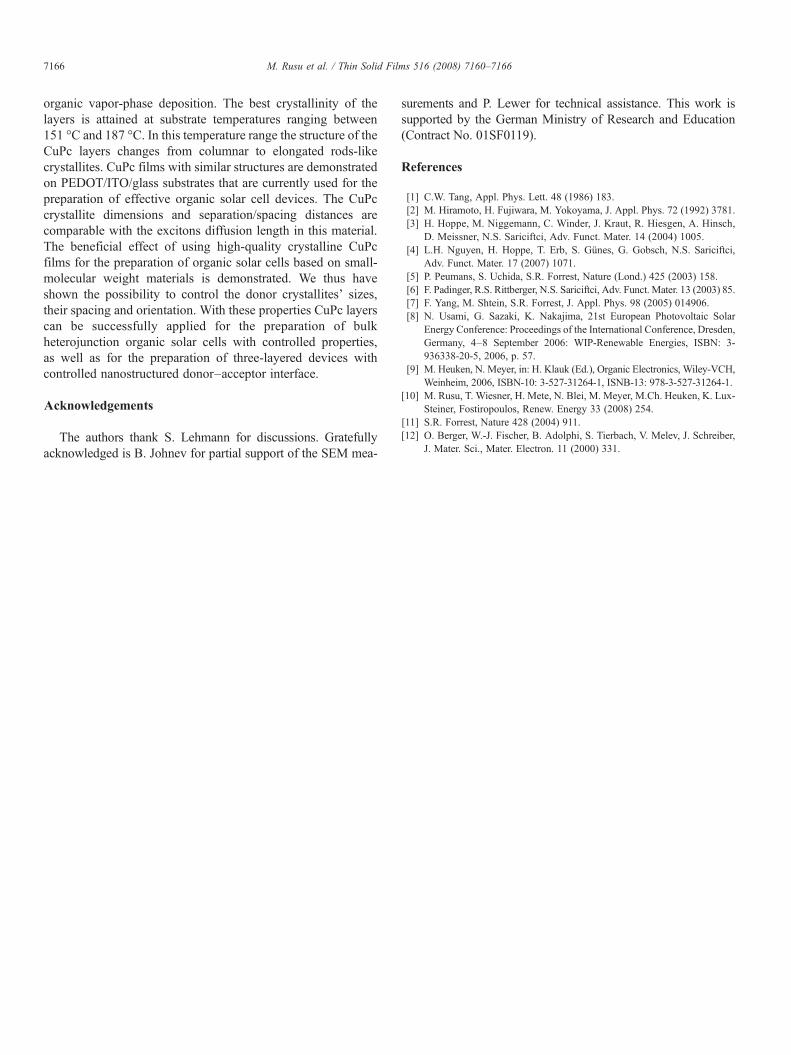
XRD measurements in the temperature range of 151–187 °C(see Sections 3.2 and 3.3) showed that elevated temperaturespreserve the b100N preferential orientation of the α-CuPc filmsdeposited on both Si(200) and PEDOT/ITO/glass substrates. Hightemperatures improve the alignment perfection of the b-stacking-axis of CuPc molecules in parallel orientation relative to the filmplain. Therefore, when analysing images of the CuPc morphologydevelopment with the substrate temperature, it can be concludedthat formation of the films' structure occurs through a coalescenceprocess. At low temperatures the filmsmorphology develops fromthe coalescence of small grains in a vertical direction until a perfectcolumnar structure is achieved. Further increase of the substratetemperature results in coalescence of the neighbour columnarcrystallites into elongated rods-like ones. Being influenced by thesubstrate temperature, the coalescence process drives the crystal-lites' shapes, dimensions and separation distances between them.By adjusting the OVPD process parameters, CuPc nanostructuredlayers with pre-required crystalline characteristics can beachieved. The analysis of the PV data in Section 3.6 helps toconclude on a preferred structure of the CuPc layers, suitable forOSC devices. Although the CuPc films deposited at elevatedtemperatures of ~190 °C show a higher degree of (200)-texturing,it seems that CuPc films deposited at temperatures ~150 °C bettermatch the requirements of an effective organic solar cell. The laterfilms have a columnar structure with inter-columnar distancescomparable to their diameters or smaller. In contrast, the filmsdeposited at high temperatures possess larger lateral dimensionsand bigger spacings between rods-like crystallites. Theseincreased dimensions may affect the transport properties of thelayers and effectiveness of the excitons diffusion to the DAinterface in complete OSCs. The slight decrease of the OSCsparameters observed at high temperaturesmay be explained by theabove factors. Alteration of the devices short-circuit current andfill factors at temperatures below 150 °C can be interpreted interms of lower degree of CuPc crystallinity, e.g., columnarcrystallites consisting of small CuPc grains. Along with the abovefactors, the effects of temperature related to the ITO/PEDOT andPEDOT/CuPc interfaces are not excluded.
5. Conclusion
We have demonstrated b100N highly oriented α-phase CuPclayers on Si(200) substrates by employing the technology of
7166 M. Rusu et al. / Thin Solid Films 516 (2008) 7160–7166
organic vapor-phase deposition. The best crystallinity of thelayers is attained at substrate temperatures ranging between151 °C and 187 °C. In this temperature range the structure of theCuPc layers changes from columnar to elongated rods-likecrystallites. CuPc films with similar structures are demonstratedon PEDOT/ITO/glass substrates that are currently used for thepreparation of effective organic solar cell devices. The CuPccrystallite dimensions and separation/spacing distances arecomparable with the excitons diffusion length in this material.The beneficial effect of using high-quality crystalline CuPcfilms for the preparation of organic solar cells based on small-molecular weight materials is demonstrated. We thus haveshown the possibility to control the donor crystallites' sizes,their spacing and orientation. With these properties CuPc layerscan be successfully applied for the preparation of bulkheterojunction organic solar cells with controlled properties,as well as for the preparation of three-layered devices withcontrolled nanostructured donor–acceptor interface.
Acknowledgements
The authors thank S. Lehmann for discussions. Gratefullyacknowledged is B. Johnev for partial support of the SEM mea-
surements and P. Lewer for technical assistance. This work issupported by the German Ministry of Research and Education(Contract No. 01SF0119).
References
[1] C.W. Tang, Appl. Phys. Lett. 48 (1986) 183.[2] M. Hiramoto, H. Fujiwara, M. Yokoyama, J. Appl. Phys. 72 (1992) 3781.[3] H. Hoppe, M. Niggemann, C. Winder, J. Kraut, R. Hiesgen, A. Hinsch,
D. Meissner, N.S. Sariciftci, Adv. Funct. Mater. 14 (2004) 1005.[4] L.H. Nguyen, H. Hoppe, T. Erb, S. Günes, G. Gobsch, N.S. Sariciftci,
Adv. Funct. Mater. 17 (2007) 1071.[5] P. Peumans, S. Uchida, S.R. Forrest, Nature (Lond.) 425 (2003) 158.[6] F. Padinger, R.S. Rittberger, N.S. Sariciftci, Adv. Funct. Mater. 13 (2003) 85.[7] F. Yang, M. Shtein, S.R. Forrest, J. Appl. Phys. 98 (2005) 014906.[8] N. Usami, G. Sazaki, K. Nakajima, 21st European Photovoltaic Solar
Energy Conference: Proceedings of the International Conference, Dresden,Germany, 4–8 September 2006: WIP-Renewable Energies, ISBN: 3-936338-20-5, 2006, p. 57.
[9] M. Heuken, N. Meyer, in: H. Klauk (Ed.), Organic Electronics, Wiley-VCH,Weinheim, 2006, ISBN-10: 3-527-31264-1, ISNB-13: 978-3-527-31264-1.
[10] M. Rusu, T. Wiesner, H. Mete, N. Blei, M. Meyer, M.Ch. Heuken, K. Lux-Steiner, Fostiropoulos, Renew. Energy 33 (2008) 254.
[11] S.R. Forrest, Nature 428 (2004) 911.[12] O. Berger, W.-J. Fischer, B. Adolphi, S. Tierbach, V. Melev, J. Schreiber,
J. Mater. Sci., Mater. Electron. 11 (2000) 331.
Copyright © 2022 FDOKUMEN