FGMOSFET circuit for Neuron Activation Function and its derivative
6
978-1-4244-2800-7/09/$25.00 ©2009 IEEE ICIEA 2009 FGMOSFET Circuit for Neuron Activation Function and its Derivative V. Suresh Babu, Salini Devi R., Ambika Sekhar and M. R. Baiju Dept. of Electronics and Communication, College of Engineering, Trivandrum, Kerala [email protected] Abstract—This paper presents Floating Gate MOSFET (FGMOSFET) circuit for generating Neuron Activation Function (NAF) and Derivative of Neuron Activation Function (DNAF) with programmable characteristics. NAF represents output of a single neuron. DNAF is needed in the training phase of neural networks. This circuit uses only FGMOSFETs to realize the NAF and DNAF. This circuit is designed to operate both in saturation region and sub-threshold region. The performance of this circuit is compared with that of CMOS based NAF DNAF circuit. The comparative study includes linear range, temperature dependence, power dissipation, supply voltage and output resistance. The simulations are done using the tanner tool. The layout of the circuit is also presented. This paper also presents analytical study of proposed circuit and FGMOSFET current mirror in saturation region. Index Terms— Floating Gate MOSFET, Neuron Activation Function, Derivative of Neuron Activation Function I. INTRODUCTION Artificial neural networks can be easily implemented in analog platforms than in digital platforms. The basic building block of neural network is the neuron. Output of a single neuron is represented using Neuron Activation Function (NAF). Derivative of Neuron Activation Function (DNAF) is used in the training phase of neural networks [1]-[2]. The different types of NAFs are sigmoid, exponential, thresholding etc. Usually tranconductance elements using the differential amplifiers are used for realizing circuits with sigmoid NAF characteristics [1]-[5]. The DNAF can be realized using the approximate derivative function [4]. Asymmetry in differential pair is used to realize the DNAF. The asymmetry can be introduced in many ways such as asymmetry due to offset voltage [2], [4], asymmetry in threshold voltages and asymmetry in area. The asymmetric cross coupled differential amplifiers are used for realizing DNAF [6]. The cross coupled differential amplifiers give better linearity [7]. Floating Gate MOSFET (FGMOSFET) based cross coupled differential amplifiers presented in this paper uses asymmetry in threshold voltages to realize the DNAF. The asymmetry in the threshold voltage is realized by varying the bias voltage applied to the FGMOSFETs. This is because the FGMOSFETs have excellent programmable characteristics and charge retention property [8]-[11]. Its threshold voltage can be adjusted by varying the voltage given to control gates. The paper also presents analytical study of the proposed circuit and FGMOSFET current mirror. II. PROPOSED CIRCUIT FOR NAF AND DNAF The circuit diagram of the proposed circuit for NAF and DNAF is shown in fig. 1. The circuit uses cross coupled differential pair configuration formed by F N1 and F N2 and F N3 and F N4 . P channel FGMOSFET current mirrors are used to drive cross coupled differential pair. Using this circuit log sigmoid and tan sigmoid NAF with varying slope and threshold levels and the corresponding derivative can be generated simultaneously. III. ANALYSIS OF PROPOSED CIRCUIT Referring to fig. 1, let I DN1 and I DN2 be the currents flowing through the FGMOSFETs F N1 and F N2 respectively. Also I DN3 and I DN4 are the currents flowing through the FGMOSFETs F N3 and F N4 respectively. I DN1 is given by (1). ( ) 2 1 1 DN FGS TN I V V β = − (1) where 2 n ox CW L μ β = and V TN1 is the threshold voltage of the FGMOSFET F N1. For the analysis of the proposed circuit, the equivalent circuit model of FGMOSFET in fig. 2 is used [12]. Figure 1. FGMOSFET circuit for realizing NAF and DNAF. 739
-
Upload
independent -
Category
Documents
-
view
6 -
download
0
Transcript of FGMOSFET circuit for Neuron Activation Function and its derivative
978-1-4244-2800-7/09/$25.00 ©2009 IEEE ICIEA 2009
FGMOSFET Circuit for Neuron Activation Function and its Derivative
V. Suresh Babu, Salini Devi R., Ambika Sekhar and M. R. Baiju Dept. of Electronics and Communication,
College of Engineering, Trivandrum, Kerala
Abstract—This paper presents Floating Gate MOSFET (FGMOSFET) circuit for generating Neuron Activation Function (NAF) and Derivative of Neuron Activation Function (DNAF) with programmable characteristics. NAF represents output of a single neuron. DNAF is needed in the training phase of neural networks. This circuit uses only FGMOSFETs to realize the NAF and DNAF. This circuit is designed to operate both in saturation region and sub-threshold region. The performance of this circuit is compared with that of CMOS based NAF DNAF circuit. The comparative study includes linear range, temperature dependence, power dissipation, supply voltage and output resistance. The simulations are done using the tanner tool. The layout of the circuit is also presented. This paper also presents analytical study of proposed circuit and FGMOSFET current mirror in saturation region.
Index Terms— Floating Gate MOSFET, Neuron Activation Function, Derivative of Neuron Activation Function
I. INTRODUCTION Artificial neural networks can be easily implemented in
analog platforms than in digital platforms. The basic building block of neural network is the neuron. Output of a single neuron is represented using Neuron Activation Function (NAF). Derivative of Neuron Activation Function (DNAF) is used in the training phase of neural networks [1]-[2]. The different types of NAFs are sigmoid, exponential, thresholding etc.
Usually tranconductance elements using the differential amplifiers are used for realizing circuits with sigmoid NAF characteristics [1]-[5]. The DNAF can be realized using the approximate derivative function [4]. Asymmetry in differential pair is used to realize the DNAF. The asymmetry can be introduced in many ways such as asymmetry due to offset voltage [2], [4], asymmetry in threshold voltages and asymmetry in area. The asymmetric cross coupled differential amplifiers are used for realizing DNAF [6]. The cross coupled differential amplifiers give better linearity [7].
Floating Gate MOSFET (FGMOSFET) based cross coupled differential amplifiers presented in this paper uses asymmetry in threshold voltages to realize the DNAF. The asymmetry in the threshold voltage is realized by varying the bias voltage applied to the FGMOSFETs. This is because the FGMOSFETs have excellent programmable characteristics and charge
retention property [8]-[11]. Its threshold voltage can be adjusted by varying the voltage given to control gates.
The paper also presents analytical study of the proposed circuit and FGMOSFET current mirror.
II. PROPOSED CIRCUIT FOR NAF AND DNAF The circuit diagram of the proposed circuit for NAF and
DNAF is shown in fig. 1. The circuit uses cross coupled differential pair configuration formed by FN1 and FN2 and FN3 and FN4. P channel FGMOSFET current mirrors are used to drive cross coupled differential pair. Using this circuit log sigmoid and tan sigmoid NAF with varying slope and threshold levels and the corresponding derivative can be generated simultaneously.
III. ANALYSIS OF PROPOSED CIRCUIT Referring to fig. 1, let IDN1 and IDN2 be the currents flowing
through the FGMOSFETs FN1 and FN2 respectively. Also IDN3 and IDN4 are the currents flowing through the FGMOSFETs FN3 and FN4 respectively. IDN1 is given by (1).
( )21 1DN FGS TNI V Vβ= − (1)
where 2
n oxC WL
μβ = and VTN1 is the threshold voltage of the
FGMOSFET FN1. For the analysis of the proposed circuit, the equivalent circuit model of FGMOSFET in fig. 2 is used [12].
Figure 1. FGMOSFET circuit for realizing NAF and DNAF.
739
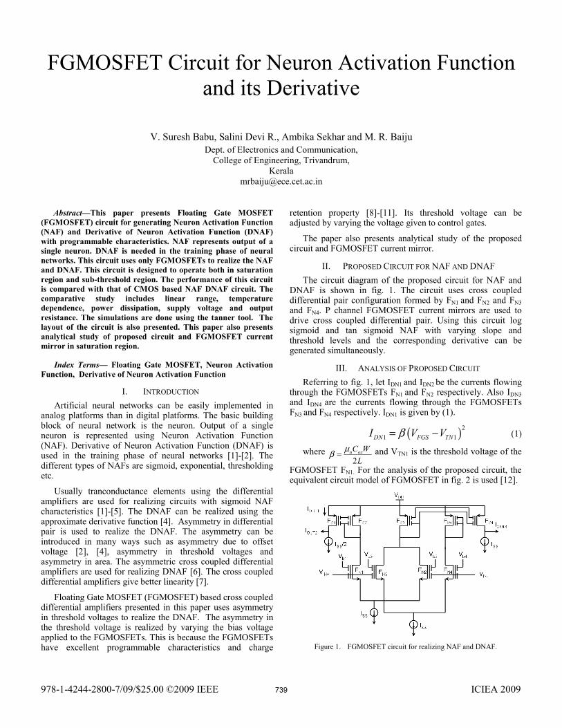
Figure 2. The detailed equivalent circuit of an n channel FGMOSFET.
The total capacitance, as seen by the floating gate is given by (2).
1
N
T GD GS GB ii
C C C C C=
= + + +∑ (2)
The floating gate input voltage is given by (3).
1
Ni GD GB GS FG
FG i D B Si T T T T T
C C C C QV V V V VC C C C C=
= + + + +∑ (3)
In (3), QFG represents charge in the floating gate. Computing the floating gate voltage with respect to the source terminal [12], VFGS is given by (4).
1
Ni GD GB FG
FGS is DS BSi T T T T
C C C QV V V VC C C C=
= + + +∑ (4)
By substituting the value of VFGS, (1) can be modified to (5).
2
1 11
Ni GD GB FG
DN is DS BS TNi T T T T
C C C QI V V V VC C C C
β=
⎛ ⎞= + + + −⎜ ⎟
⎝ ⎠∑ (5)
Neglecting QFG and the effect of the parasitic capacitances such as CGD and CGB, (5) can be modified to (6).
2
1 11
Ni
DN is TNi T
CI V VC
β=
⎛ ⎞= −⎜ ⎟
⎝ ⎠∑ (6)
For two input FGMOSFET, (6) reduces to (7).
2
1 21 1 2 1DN s s TN
T T
C CI V V VC C
β⎛ ⎞
= + −⎜ ⎟⎝ ⎠
(7)
With reference to fig. 1, the input terminal V1 is used for biasing i.e. V1s of FN1 is represented by Vb1 and V1s of FN2 is represented by Vb2. Also V2 is used for input i.e. V2s of FN1 is represented by VIN+ and V2s of FN2 is represented by VIN-. Assume that both FGMOSFETs are identical. Therefore the input capacitance values, transconductance parameters and threshold voltages are equal. So IDN1 is obtained as in (8).
2
2 11 1 1DN IN TN b
T T
C CI V V VC C
β +
⎛ ⎞⎛ ⎞= − −⎜ ⎟⎜ ⎟⎜ ⎟⎝ ⎠⎝ ⎠
(8)
Similarly IDN2 can be represented by (9).
2
2 12 2 2DN IN TN b
T T
C CI V V VC C
β −
⎛ ⎞⎛ ⎞= − −⎜ ⎟⎜ ⎟⎜ ⎟⎝ ⎠⎝ ⎠
(9)
where VTN2 is the threshold voltage of the FGMOSFET FN2. As the FGMOSFETs FN1 and FN2 are identical, VTN1= VTN2 =VT.
Hence rearranging the terms in (8) and (9), (10) and (11) are obtained.
2 2 12
DNIN T b
T T
I C CV V VC Cβ −
⎛ ⎞⎛ ⎞= − −⎜ ⎟⎜ ⎟⎜ ⎟⎝ ⎠⎝ ⎠
(10)
1 2 11
DNIN T b
T T
I C CV V VC Cβ +
⎛ ⎞⎛ ⎞= − −⎜ ⎟⎜ ⎟⎜ ⎟⎝ ⎠⎝ ⎠
(11)
Subtracting (10) from (11), and substituting VIN+ -VIN-=VDI and Vb1- Vb2 = ∆Vb12, (12) is obtained.
1 2 2 112
DN DNDI b
T T
I I C CV VC Cβ β
⎛ ⎞ ⎛ ⎞− = + Δ⎜ ⎟ ⎜ ⎟
⎝ ⎠ ⎝ ⎠ (12)
From (12), the differential input voltage, VDI can be estimated as given by (13).
( ) 11 2 12
22
TDI DN DN b
C CV I I VCC β
= − − Δ (13)
Rearranging (13), (14) is obtained.
( )1 2 1 12 2DN DN b DIT
I I C V C VC
β− = Δ + (14)
Squaring both sides of (14) and substituting IDN1 + IDN2 = ISS, expression for IDN1IDN2 is obtained as in (15).
( )( )
2
21 2 1 12 222 2
SSDN DN b DI
T
II I C V C VCβ⎛ ⎞
⎜ ⎟= − Δ +⎜ ⎟⎝ ⎠
(15)
IDN1IDN2 can also be expressed as in (16).
( ) ( )( )2 21 2 1 2 1 2
14DN DN DN DN DN DNI I I I I I= + − − (16)
Equating (15) and (16), IDN1 - IDN2 can be obtained as in (17).
( )( )
( )( )
22 4
1 2 1 12 2 1 12 22 4
2 SSDN DN b DI b DI
T T
II I C V C V C V C VC C
β β⎛ ⎞ ⎛ ⎞⎜ ⎟ ⎜ ⎟− = Δ + − Δ +⎜ ⎟ ⎜ ⎟⎝ ⎠ ⎝ ⎠
(17)
From fig. 1, IDN1+ IDN2=ISS. So the expression for IDN1 and IDN2 are obtained as in (18) and (19).
( ) ( )2
2 41 1 12 2 1 12 22 4 2
212SS
DN b DI b DIT SS T SS
II C V C V C V C VC I C I
β β⎛ ⎞= + Δ + − Δ +⎜ ⎟⎜ ⎟
⎝ ⎠
(18)
( ) ( )2
2 42 1 12 2 1 12 22 4 2
212SS
DN b DI b DIT SS T SS
II C V C V C V C VC I C I
β β⎛ ⎞= − Δ + − Δ +⎜ ⎟⎜ ⎟
⎝ ⎠
(19)
Expression for IDN1 and IDN2 can be modified as given in (20) and (21).
( ) ( )21 12 21 1 12 221 2
2b DISS
DN b DIT SST SS
C V C VII C V C VC IC I
β β⎛ ⎞Δ += + − Δ +⎜ ⎟⎜ ⎟
⎝ ⎠
(20)
740

( ) ( )21 12 22 1 12 221 2
2b DISS
DN b DIT SST SS
C V C VII C V C VC IC I
β β⎛ ⎞Δ += − − Δ +⎜ ⎟⎜ ⎟
⎝ ⎠
(21)
Similarly the expression for IDN3 and IDN4 as in (22) and (23) can also be obtained.
( ) ( )21 34 23 1 34 221 2
2b DISS
DN b DIT SST SS
C V C VII C V C VC IC I
β β⎛ ⎞Δ += + − Δ +⎜ ⎟⎜ ⎟
⎝ ⎠
(22)
( ) ( )21 34 24 1 34 221 2
2b DISS
DN b DIT SST SS
C V C VII C V C VC IC I
β β⎛ ⎞Δ += − − Δ +⎜ ⎟⎜ ⎟
⎝ ⎠
(23)
where ∆Vb34=Vb3-Vb4.
A plot of IDN1 versus VDI with ∆Vb12=0 is shown in fig. 3. When ∆Vb12 is positive, IDN1 shifts towards left and when ∆Vb12 is negative, IDN1 shifts towards right. Thus by varying ∆Vb12, NAFs with varying threshold levels are obtained.
According to (13), VDI became zero when ∆Vb12=0, IDN1=ISS/2 and IDN2= ISS/2.
When FN1 conducts, IDN1=ISS and IDN2=0, therefore VDIMAX is given by (24).
2
SSTDIMAX
ICVC β
= (24)
When FN2 conducts, IDN1= 0 and IDN2= ISS, therefore VDIMIN is given by (25).
2
SSTDIMIN
ICVC β
= − (25)
The linear range is given by (26) and (27).
Linear range = DIMAX DIMINV V− (26)
2
2 SST ICC β
= (27)
In fig. 1 IOUT1 equals the current through one of the differential pairs and it represents log sigmoid NAF as given by (20) and (28). IOUT2 represents tan sigmoid NAF by subtracting a dc current from log sigmoid function as given by (29). A plot of IOUT2 versus VDI is represented by (29) is as shown in fig. 4.
1 1OUT DNI I= (28)
2 1 2
SSOUT DN
II I= − (29)
By the principle of difference approximation, DNAF can be obtained as the difference of currents in the two cross coupled differential pairs. The difference in currents can be introduced by creating a mismatch between the differential pairs.
Figure 3. IDN1 versus differential input voltage, VDI of the proposed circuit.
Figure 4. IOUT2 versus differential input voltage, VDI of the proposed circuit.
In the present work, this mismatch is introduced by a difference in threshold voltages between the transistors of two differential pairs. This is done by changing the relative values of bias voltages applied to the differential pairs. This introduces a difference in the currents through the differential pairs. Hence IOUT3 represents DNAF function as given by (30) to (32). The scaling factor of the DNAF can be varied by varying the difference in currents between the two differential pairs. This is achieved by varying the difference in bias voltages between the differential pairs.
3 2 3OUT DN DN SSI I I I= + − (30)
3 1DN DNI I= − (31)
( ) ( )
( ) ( )
23 1 34 2 1 34 22
21 12 2 1 12 22
22
22
SSOUT b DI b DI
T T SS
SSb DI b DI
T T SS
II C V C V C V C V
C C I
IC V C V C V C V
C C I
β β
β β
⎛ ⎞= Δ + − Δ +⎜ ⎟
⎝ ⎠
⎛ ⎞− Δ + − Δ +⎜ ⎟
⎝ ⎠
(32)
When ∆Vb12 = ∆Vb34, IOUT3 is zero. When ∆Vb34 is greater than ∆Vb12, IOUT3 is positive. When ∆Vb34 is lesser than ∆Vb12, IOUT3 is negative.
A. Analysis of FGMOSFET Current Mirrors The factors that cause the current mirror to deviate from its
ideal characteristics are channel length modulation, threshold voltage offset between two transistors and geometrical mismatch. Basic circuit of FGMOSFET current mirror is shown in fig. 5.
Assume that C1 is the capacitance across the signal gate and C2 is the capacitance across the control gate. CT is the total capacitance which is given by (2). V1s is voltage at the signal gate with respect to the source. V2 is voltage at the control gate. IDa and IDb are the current flowing through the FGMOSFETs Fa and Fb. By including the channel length modulation parameter, IDa and IDb can be written as given in (33) and (34).
741

Figure 5. Basic circuit of the current mirror using FGMOSFETs.
( )2
1 21 2 1Da a s s Ta a DSa
T T
C CI V V V VC C
β λ⎛ ⎞
= + − +⎜ ⎟⎝ ⎠
(33)
( )2
1 21 2 1Db b s s Tb b DSb
T T
C CI V V V VC C
β λ⎛ ⎞
= + − +⎜ ⎟⎝ ⎠
(34)
Assuming that β is different for the two transistors and all other parameters to be identical, and taking into account the threshold offset effect between the two transistors and channel length modulation effect, IDb /IDa can be expressed by (35).
22
1 21 1
21 2
1 1
11
TS Tb S
Db b b DS
TDa a a DSS Ta S
C CV V VI VC C
C CI VV V VC C
β λβ λ
⎛ ⎞− +⎜ ⎟⎛ ⎞ ⎛ ⎞ ⎛ ⎞+⎜ ⎟=⎜ ⎟ ⎜ ⎟ ⎜ ⎟+⎜ ⎟⎝ ⎠ ⎝ ⎠ ⎝ ⎠− +⎜ ⎟⎝ ⎠
(35)
Rearranging (35) and substituting the following parameters.
2
a bβ ββ += , b aβ β βΔ = − ,
2
Ta TbT
V VV += , T Tb TaV V VΔ = − , and
2
a bλ λλ += , b aλ λ λΔ = − .
In (35), neglecting the higher order components and assuming λVDS is less than unity, IDb /IDa is obtained as in (36).
1
21 2
1 1
21
TT
DbDS
TDaS S T
C VI C VC CI V V V
C C
β λβ
⎛ ⎞Δ⎜ ⎟⎛ ⎞ ⎛ ⎞Δ ⎜ ⎟= + − + Δ⎜ ⎟ ⎜ ⎟⎜ ⎟⎝ ⎠⎝ ⎠ + −⎜ ⎟⎝ ⎠
(36)
The current ratio of the FGMOSFET current mirror depends on the gate capacitances and the voltage at the input gates.
B. Subthreshold Operation of FGMOSFET The circuit gives lower power dissipation when it is
designed to operate in sub-threshold region. The drain current of an FGMOSFET in sub-threshold region is given by (37).
( )
0
FGS T
T
V VnU
DWI I eL
−
= (37)
where VFGS is the floating gate voltage as given by (4). UT is the thermal voltage and VT is the threshold voltage. I0 is the process dependent constant. n is a parameter that depend on the threshold voltage and the slope of IDS versus VGS characteristics of FGMOSFET in sub-threshold.
IV. SIMULATION RESULTS The layout of the proposed circuit in saturation region using
the tanner L. Edit is shown in fig. 6.
Fig. 7 shows the T. Spice simulation results obtained using a supply voltage of 0.7V and bias voltages Vb1=Vb2=Vb4 of 0.1V and Vb3 of 0.2V. The scaling factor of the DNAF can be varied by varying the bias voltage Vb3. Fig. 8 shows the NAF and DNAF output obtained from the CMOS circuit in [6]. Fig. 9 shows the NAF and DNAF output obtained from the proposed circuit in sub-threshold region. The linear range in fig. 9 is less compared to that of fig. 7 and fig. 8. Also the output current is of the order of nanoamperes. But the output current of the proposed circuit in saturation is of the order of microamperes. Also the linear range of the proposed circuit in saturation is 700mV whereas the linear range of CMOS circuit is only 400mV.
The threshold of the NAF can be varied by varying the difference in the bias voltage applied to the first differential pair FN1 and FN2 i.e. by varying ∆Vb12. The threshold variation is as shown in the fig. 10. The slope of the NAF can be varied by varying the bias voltages applied to FN1, FN3. The slope variations are shown in the fig. 11. The proposed circuit produces both tan sigmoid and log sigmoid NAF as shown in fig. 12. So the simulation results match with the analytical results.
Figure 6. Layout of the proposed FGMOSFET circuit for NAF and DNAF
in saturation region.
Figure 7. NAF and DNAF output obtained from the proposed circuit in
saturation region.
742

Figure 8. NAF and DNAF output obtained from the CMOS circuit in
saturation region.
Figure 9. NAF and DNAF output obtained from the proposed circuit in
subthreshold region.
Figure 10. NAF output with varying threshold level obtained from the
proposed circuit.
Figure 11. NAF output with varying slope level obtained from the proposed
circuit.
Figure 12. Log sigmoid and tan sigmoid NAF obtained from the proposed
circuit.
The temperature dependence of the proposed circuit in saturation is also very less as in the fig. 13. The NAF and DNAF curves are plotted for various temperatures from 100C to 600C with increments of 100C. Fig. 13 shows that the variation of NAF and DNAF curves with change in temperature is very less. The NAF and DNAF curves of the CMOS circuit in [6] in the saturation region are plotted for the same temperature variations as that of proposed circuit. The resulting curve is shown in fig. 14. The temperature dependence of the proposed circuit in the sub-threshold region is shown in fig. 15.
Figure 13. NAF and DNAF output in saturation region for temperatures from
100C to 600C with an increment of 100C.
Figure 14. NAF and DNAF output of CMOS circuit for temperatures from 100C to 600 C with an increment of 100C.
743
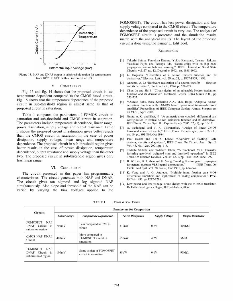
Figure 15. NAF and DNAF output in subthreshold region for temperatures from 100C to 600C with an increment of 100C.
V. COMPARISON Fig. 13 and fig. 14 shows that the proposed circuit is less
temperature dependent compared to the CMOS based circuit. Fig. 15 shows that the temperature dependence of the proposed circuit in sub-threshold region is almost same as that of proposed circuit in saturation.
Table 1 compares the parameters of FGMOS circuit in saturation and sub-threshold and CMOS circuit in saturation. The parameters include temperature dependence, linear range, power dissipation, supply voltage and output resistance. Table 1 shows the proposed circuit in saturation gives better results than the CMOS circuit in saturation in the case of power dissipation, supply voltage, linear range and temperature dependence. The proposed circuit in sub-threshold region gives better results in the case of power dissipation, temperature dependence, output resistance and supply voltage than the other two. The proposed circuit in sub-threshold region gives only less linear range.
VI. CONCLUSION The circuit presented in this paper has programmable
characteristics. The circuit generates both NAF and DNAF. The circuit gives tan sigmoid and log sigmoid NAF simultaneously. Also slope and threshold of the NAF can be varied by varying the bias voltages applied to the
FGMOSFETs. The circuit has less power dissipation and less supply voltage compared to the CMOS circuit. The temperature dependence of the proposed circuit is very less. The analysis of FGMOSFET circuit is presented and the simulation results match with the analytical results. The layout of the proposed circuit is done using the Tanner L. Edit Tool.
REFERENCES
[1] Takeshi Shima, Tomohisa Kimura, Yukio Kamatani, Tetsuro Itakura, Yasuhiko Fujita and Tetsuya Iida, “Neuro chips with on-chip back propagation and/or hebbian learning.”, IEEE Journal of Solid State Circuits, vol. 27, no. 12, December 1992, pp. 1868-1992.
[2] G. Bogason, “Generation of a neuron transfer function and its derivatives,” Electron. Lett., vol. 29, no.21, p. 1867-1869, 1993.
[3] Annema. A. J.: ‘Hardware realization of a neuron transfer function and its derivative’, Electron. Lett., 1994, pp.576-577.
[4] Chun Lu and Shi B. “Circuit design of an adjustable Neuron activation function and its derivative”. Electronic Letters. 36(6) March 2000, pp 553-555.
[5] V.Suresh Babu, Rose Katharine A.A., M.R. Baiju, “Adaptive neuron activation function with FGMOS based operational transconductance amplifier”,Proceedings of IEEE Computer Society Annual Symposium on VLSI , April 2008.
[6] Gupta, A. K., and Bhat, N.: ‘Asymmetric cross-coupled differential pair configuration to realize neuron activation function and its derivative’, IEEE Trans. Circuit Syst. II, Express Briefs, 2005, 52, (1), pp. 10-13.
[7] A. Nedungadi and T. R. Viswanathan, “Design of linear CMOS transconductance elements,” IEEE Trans. Circuits syst., vol. CAS-31, no. 10, pp. 891-894, Oct.1984.
[8] Paul Hasler and Tor S. Lande, “Overview of floating- Gate devices, circuits and systems”, IEEE Trans. On Circuit. And Syst.II Vol. 48, No.1, Jan. 2001, pp. 1-3.
[9] Tadashi Shibata and Tadahiro Ohmi, “A functional MOS transistor featuring gate-level weighted sum and threshold operations” in IEEE Trans. On Electron Devices, Vol. 39, no. 6, pp. 1444-1455, June 1992.
[10] B. W. Lee, B. J. Sheu and H. Yang, “Analog floating gate synapses for general purpose VLSI neural computation,” IEEE Trans. On Circts. And Syst. Vol. 38, No. 6, June 1991, pp. 654-647.
[11] K. Yang and A. G. Andreou, “Multiple input floating gate MOS differential amplifiers and applications of analog computation”, Proc. ISCAS 1992, pp.1212-1216.
[12] Low power and low voltage circuit design with the FGMOS transistor, Dr Esther Rodriguez villegas, IET publishers,2006.
TABLE I. COMPARISON TABLE
Circuits Parameters for Comparison
Linear Range Temperature Dependence Power Dissipation Supply Voltage Output Resistance
FGMOSFET NAF DNAF Circuit in saturation region
700mV Less compared to CMOS circuit 310nW 0.7V 400KΩ
CMOS NAF DNAF Circuit
400mV More compared to FGMOSFET circuit in saturation
850nW 4.2V 5MΩ
FGMOSFET NAF DNAF Circuit in subthreshold region
100mV Same as that of FGMOSFET circuit in saturation 88pW 0.1V 90MΩ
744