
Enhanced dynamic range analog filter topologies with a notch/all-pass circuit example
Upload
independentCategory
view
0download
0
Analog Circuit Testing Based on Sensitivity Computation and New Circuit Modeling
Naim Ben Hamida and Bozena Kaminska &ole Polytechnique de MontrCal
P.O. Box 6079, Station A, MontrCal, PQ, Canada, H3C 3A7
Abstract Analog circuit testing is considered to be a very dif-
ficult task, due mainly to the lack of fault models and accessibility to internal nodes. An approach is pre- sented for analog circuit modeling and testing to over- come this problem. This circuit modeling is based on a sensitivity computation and on circuit structure, which are crucial in analog circuit testing. The testability of the circuit is achieved for the simple fault model and by functional testing. Component deviations are deduced by measuring a number of output parameters, and through sensitivity analysis and tolerance computation. Using this approach, adequate tests are identified for testing both catastrophic and soft faults. Some experi- mental results are presented.
1.0 Introduction Faults in analog circuits can be categorized as cata-
strophic or parametric (soft) faults. Catastrophic faults are open and short circuits caused by sudden and large variations in components [81. Parametric or soft faults are defined by the circuit’s functionality. Here, a param- eter deviates continuously with time or environmental conditions to unacceptable values 19- 111. In analog cir- cuits, the concern is which parameters to select for test- ing, and the accuracy to which they should be tested in order to detect the variations in the faulty components.
Eunctional testing is based on the verification of a circuit’s functionality by applying stimulus signals at the inputs and verifying its outputs. Many functional testing algorithms have been developed, among them the method presented by Sloan [ 121, in which the trans- fer function of a circuit is estimated by applying an input stimulus and observing the response. He charac- terizes a circuit as the transfer function from the circuit response to the following input stimuli: random, deter- ministic, periodic and aperiodic waveforms. Once the transfer function of a good circuit has been established, the circuit in question can be tested by comparing its transfer function with that of the good circuit.
Dai and Souders 1101 present an approach for the functional testing and parameter estimation of analog circuits in the time domain. This approach extends the analysis of linear circuits to include nonlinear circuits. An algorithm proposed by Milor and Sangiovanni [131 automatically generates analog circuit test sets that min- imize testing time. The algorithm reduces the functional test sets to include only those that determine whether or not a circuit contains parametric faults. Chin [91 com- bines examination of the transient response to step inputs with multivariable discriminant analysis to dis- tinguish a good circuit from a bad one.
Unlike these time domain approaches, a model developed by McKeon and Wakeling 1141 tests analog circuits by measuring the DC voltage at different nodes. The relationship between the parameters, such as volt- age and current, at component interconnections repre- sents their behavior. This model deduces the values of parameters within the circuit by propagating the effect of measurement through this model. Faults are inferred from the detection of inconsistencies and located by sus- pending constraints with the model.
In this work, we propose a simple new method for the production testing of analog circuits. Earlier efforts were mainly focused on diagnostic testing. Our research can be distinguished ftom the earlier works by our use of different types of input stimuli and the measurement of different kinds of output parameters. Each of the pre- vious methods uses only one specific type of measure- ment or input stimulus which is based on time domain, harmonic or static measurements. We combine these three categories of measurements to increase the amount of information available to predict whether the circuit is defective or not. In addition, our model treats the circuit under test in a goho-go manner and lets us treat all errors. ranging from response deviation due to toler- ances to catastrophic faults. Another important aspect of our approach is that we can predict the testability of the circuit by sensitivity analysis and, consequently apply a design-for-testability technique.
In this paper, our main interest is simple-fault detec- tion. Based on the sensitivity computation presented in [1,21, a method for parametric and catastrophic fault detection is developed. This method is an extension of the work presented in [1,21. where a diagnostic tech- nique was proposed. First, the objectives of this work are defined. Next, a sensitivity graph model represent- ing the relation between parameters, components and measurement points is introduced. The analog circuit testing problem is then defined, and some solutions are presented in section 4. Some experimental studies are included and, finally, our concluding remarks.
2.0 Objectives Test requirements may be divided into three related
but distinct classifications: design characterization, diagnostics and production testing. Design characteriza- tion tests are the procedures that the design engineers perform to determine whether or not their design meets the design specifications, while diagnostic testing is conducted when a device fails to meet its required per- formance specifications and the cause of the failure must be discovered. The topic of this paper focuses on the production testing that is performed on ICs undergo- ing fabrication and manufacturing to determine whether or not they are of acceptable quality. The approach
Paper 32.1 652
INTERNATIONAL TEST CONFERENCE 1993 0-7803-1 429-8193 $3.00 1993 IEEE
adopted in this work is to performance of functional testing of analog circuits.
In production testing, we need to know if the circuit contains at least one defect and must therefore be declared faulty. Thus, a simple fault model is sufficient for test generation in order to separate fault-free from faulty circuits. This model supposes that a defective cir- cuit contains only one fault. Based on functionality, functional analog circuit testing consists in verifying whether or not all the specifications of the circuit are met. This can be done by applying stimulus signals at the inputs and verifying its outputs. This method is not practical for ICs due to the lack of accessibility to inter- nal nodes and the number of parameters that should be tested. In fact, we need to test all the parameters to be sure that the circuit is fault-free. By “parameters” we mean not only the functions realized at the outputs of the circuit, but also the intermediate functions. So, to avoid complexity, what we need to do is to test only some of the parameters, such that the remaining param- eters will be covered. The question is therefore, how do we choose the parameters to be tested or measured?
We know that the circuit’s parameters depend on the circuit’s elements. Note that the parameters are the functions realized by the circuit. For example, the gain of an amplifier is a function of the set of transistor char- acteristics, resistors, capacitances, etc. If we are sure that all the elements on which the gain depends are fault-free, then we are sure that the amplifier’s gain is fault-free. Furthermore, if we are sure that all the parameters of the amplifier are fault-free, then the amplification circuit is fault-free. So, to test an analog circuit, we should test all the elements that make up the circuit.
The question now becomes, is how do we test the elements of the circuit?
To answer this question, we need a simple relation between the elements and the parameters that represents the functionality of the circuit. and we also need other information about the structure of the circuit. First-order sensitivity is the appropriate relation between the ele- ments and parameters. In fact, sensitivity is the ratio of the relative deviation of the parameter to the relative deviation of the element. In other words, it represents the parameter deviation due to the element deviation. The principal advantage of the sensitivity relation is its simplicity. This relation can in fact be computed experi- mentally and without handling the complicated transfer functions of the circuit. This computation is carried out once in the simulation phase.
The second piece of information that we need is structural. By “structural information” we mean the relation between primary outputs and parameters. This information can be extracted easily from the circuit topology. With the relation between the elements and parameters of a circuit and knowing the structure of the circuit, we have enough information to build the circuit graph. This graph is then used to develop an appropriate test set. Finding a test for the element of the circuit con- sists in finding a set of parameters to be measured that
guarantees maximum fault coverage of the elements and, incidentally, gives maximum fault coverage for the other parameters.
We propose a test strategy that consists of the fol- lowing four steps: the circuit’s sensitivity is computed (step 1); the circuit graph is constructed (step 2); this graph is used to determine which performances should be measured to guarantee a maximal coverage of the circuit’s elements (step 3); once the test set has been found, the quality of the test is evaluated (step 4). This evaluation can be performed by computing the maximal and minimal bounds of the element error that can be detected. We will therefore discuss the element’s fault coverage for a given tolerance box. Fault coverage is estimated by computing the ratio of the faulty elements that can be detected over all the elements for a fault greater than a given tolerance value.
3.0 Sensitivity and Circuit Modeling Our interest in this paper is analog circuit testing.
Thus, we need a model for the circuit under test. In this model, the functionality and the structure of the circuit should be covered. By “functionality” we mean the rela- tion between elements and parameters. Structure is the relation between parameters and primary outputs. First- order sensitivity is a good and simple relation between elements and parameters. This relation can be computed either analytically or experimentally. The relation between parameters and primary outputs can be extracted from the circuit’s topology. Based on circuit topology and the first-order sensitivity computation, a simple model for analog circuits is built. This model is a graph representing the relation between elements, parameters and primary outputs. In this section, the first order differential and incremental sensitivity computa- tions are presented. Next, the sensitivity analysis will be used for circuit graph construction.
3.1 Sensitivity computation In the design of electrical circuits, it is important to
know the deviation in the circuit’s performance due to changes in the values of some circuit elements. The deviation in the element values with respect to their nominal values depends on the manufacturing process and the temperature of the elements. Sensitivity gives a measure of the circuit’s performance change for a change in the circuit’s element values. It helps the designer to choose adequate element tolerances. The sensitivity calculation involves determination of the first-order partial derivatives of the network functions. Sensitivity determination is a classical approach that has most often been used to examine the performance of filters. A circuit’s sensitivity of response to a compo- nent’s tolerance is an important practical consideration in the design of an RC network [31. Deviation from nominal element values can distort the response and result in an undesirable or unstable circuit. Specific designs are adopted to minimize this effect.
Note that we define the term “sensitivity” as repre- senting the effect of a change in the element xi on the resulting change in the circuit performance parameter
Paper 32.1 653
Ti [4]. We must distinguish between differential sensi- tivity, due to small variations in elements, and incre- mental sensitivity, due to a large variation in elements. Differential sensitivity is given by the following equa- tion:
- I
xi ( g + O
On the other hand, when the element x i is submit- ted to a large perturbation or deviation, the resulting change in the output parameter Ti is analyzed by the incremental sensitivity. The following equation defmes incremental sensitivity 151:
x . AT T . i j = - x - '4 T . Axi I
(2)
The incremental sensitivity can either be computed directly. fkom the transfer function of the parameter T j , or experimentally. In the first case, the transfer function of Ti can be written as a fraction, where
N (w, x) T i ( w , x ) = - , and incremental sensitivity is
D (w, x ) then given by the following equation:
PxJ = A x . D I 1+s -
i
1
xi x
(3)
D x,
where S equals the differential sensitivity of the
dominator D; STJ equals the differential sensitivity of
a rational-form parameter. In more complex circuits, sensitivity calculation is a difficult task. To avoid this difficulty. we can measure the sensitivity fkom the good circuit under simulation [21. To estimate the sensitivities
T D S and S necessary to determine the incremental
sensitivity p by measurement. we submitt component x to two devfations, ba and Ax , and then measure b the corresponding deviation values AT and AT of parameter T at the output. From equation 3. we obtain:
x,
X X T
a r!
X "a X- - - -
a (4)
T "b
X- sX - - - A Tb
m
From these two equations and after mathematical development, we obtain the following equation:
1 ATaATb X (Axa - Axb)
A X ~ A X ~ ( A T ~ - A T ~ )
ATb ATa (5) Axb Axa
ATa - ATb P = x x
By replacing SD and ST1 in equation 3 the incre- mental sensitivity can be easily computed. In the fol- lowing discussion, the incremental sensitivity will be used. In fact, with the incremental sensitivity we can treat both catastrophic and soft faults. whereas with the differential sensitivity we can only treat soft faults. In catastrophic faults, the element deviation is very large, which is why the differential sensitivity cannot be used.
3.2 Circuit modeling An analog circuit is characterized by a number of
elements x, that constitute the circuit and a number of performances (parameters) Ti that characterize the cir- cuit. The TI parameters either can or cannot be seen at the outputs of the circuit. Thus. the number of parame- ters to be measured in functional testing will be huge, and this process is not practical because of the lack of accessibility to intemal nodes. To solve this problem, we propose to test the x i elements, from the measure- ment of the output parameters instead of testing the parameters themselves. If we are sure that all the ele- ments are fault-free, then we are sure that the parame- ters are within their acceptable margin.
We propose a modeling technique in which the cir- cuit graph is composed of three kinds of nodes: primary output nodes, parameter nodes and element nodes. The circuit graph therefore has three connectivity matrices. The first is between the primary outputs. This connec- tivity matrix is extracted fiom the circuit topology, and shows which primary outputs are connected to each other. The second connectivity matrix is the relation between primary outputs and parameters. This matrix
x, x,
Paper 32.1 654
shows which parametas are measured from which out- puts. The third connectivity matrix is the relation between parameters and elements. This matrix is the sensitivity matrix. In fact, the parameters can be sensi- tive both to the elements and to other parameters. Hier- archical sensitivity analysis enables us to compute the sensitivity of one parameter relative to the variation of another, and, from this sensitivity, we can deduce the sensitivity of the parameter measured at one of the out- puts to the variation of the elements. The arcs between nodes can be explained as follows: an arc between two primary outputs means that these two outputs are related (dependent) in the circuit. If an arc between a primary output node and a parameter node exists, then the parameter can be directly measured at this output. This relation can be extracted from the circuit’s topol- ogy. An arc between a paramem and an element means that the parameter is sensitive to the element’s variation. In the circuit graph, an edge between parameter Ti and
the elements xi exists if the sensitivity S‘J is different from 0, and the sensitivity is the weight of this edge.
The following example of an amplification circuit is used to show how an analog circuit can be modeled by a sensitivity graph. The sensitivity graph represents the behavior and the structure of the circuit, which are cru- cial not only for testing but also for other applications, such us disjoint decomposition, circuit synthesis and others.
X‘
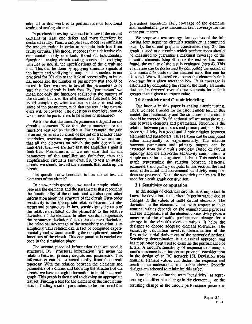
3.3 Example This example of an amplification circuit (Fig. 1).
demonstrating the application of our method in a practi- cal case, shows how the circuit can be modeled follow- ing computation of the sensitivity matrix.
Fig. 1. Amplification circuit
The parameters of this circuit are the following: A I : Gain of the first stage. A2: Gain of the high-passfilter al a knownfre- 4uency
fcl : Cut-offfrequency of the high-pass filter. A3: Gain in AC voltage of the thirdpart A4: Gain in DC voltage of the third part fc2: Cut-ofSfrequency of the low-passfilter.
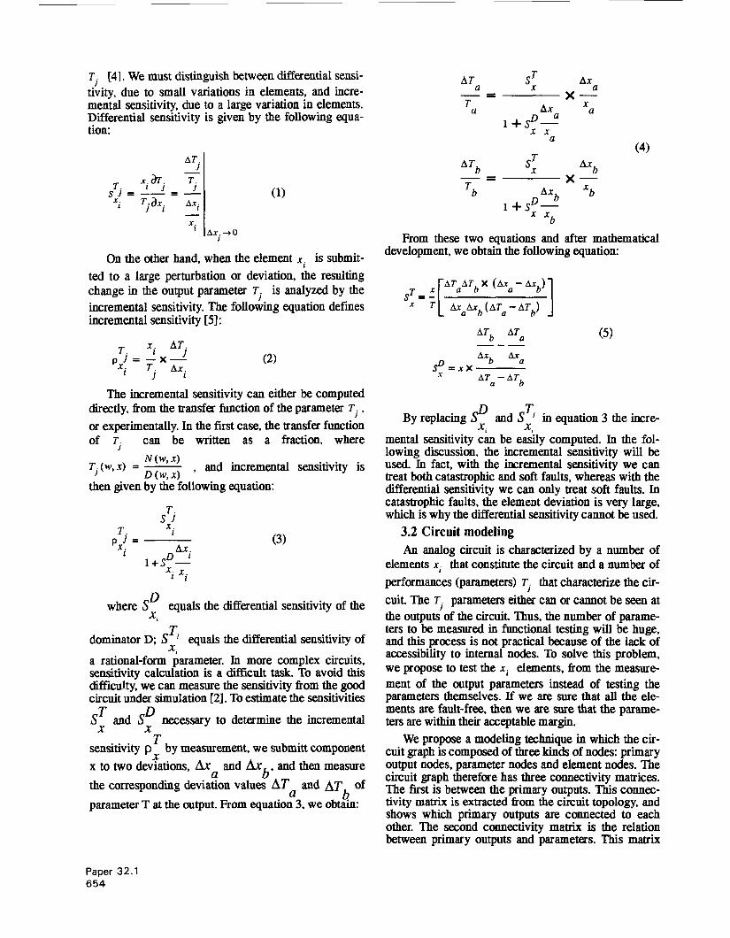
The following incremental sensitivity matrix(A) has been computed by SPICE [ 161 simulation:
0 0 0.58 0.38 0 0 0 A2
0 0 -0.91 -0.89 0 0 0 f c l
0 0 0 0 -0.96 0.48 -0.48 A3
0 0 0 0 -0.97 0.97 0 A4 0 0 0 0 0 -0.88 -0.91 f c 2
A=
R 1 R2 C1 R3 R4 R5 C2 \
The connectivity matrix representing the relation between performances and outputs (B) and the connec- tivity matrix between primary outputs(C) are as fol- lows:
[ \ 2 3 4
The resulting graph of these three connectivity matrices is shown in Fig. 2. The weights of the arcs between elements and performances are given in the sensitivity matrix A. The arrows in the graph pointing to nodes 2,3 and 4 tell us that these three nodes are the cir- cuit outputs.
Fig 2. Graph modeling of the amplification circuit
This graph is a two-level graph. In this paper, we present two kinds of graph modeling: the two level graph and the multi-level graph. The only difference between a two-level graph and a multi-level graph is that the performances in a two level-graph are in direct relation with the elements and there is no relation between performances, whereas the performances in multi-level graph are related to each other and to the elements. With hierarchical sensitivity analysis [a. the circuit can be modeled as a multi-level graph where per- formances are sensitive to each other.
In the second example. we consider the multi-level graph of the same circuit as in Fig. 1. but with output 4 only. Performances A3 and A4 (Fig. 2) cannot be mea- sured. Instead, performance A3’ and A4’ will be con- sidered which are the ratios of the voltages at points 3 and 4 respectively over the input voltage. The multi- level graph model of the analog circuit is shown in Fig.
Paper 32.1 655

3. It is clear that the DC gain (A4) cannot be measured at the output since the capacitance is considered as an open circuit in DC analysis. To measure this perfor- mance, the circuit should be modified. One possible modification would be to shorten the capacitance C1 when the DC gain A4’ is measured. This can be done by adding a transistor, working as a switch, in parallel with C1. In test mode, when we want to measure A4’. the transistor is shorted, and in normal mode the transistor is an open circuit. Fig. 3. Graph modeling of the amplijkation circuit
The twelevel graph is used in the case of small cir- cuits. while the multi-level graph more appropriate in the case of large circuits. The circuit graph model per- mits to find a test set that covers all the elements of the circuit, and in circuit testing to show which perfor- mances should be measured at which output.
4.0 Sensitivity and analog circuit testing The main factors that make analog circuit testing
difficult can be summarized as follows: Analog systems are frequently nonlinear, include
noise and have parameter values that vary widely. Thus, deterministic methods are often inefficient for modeling these systems.
Relations between input and output signals in ana- log circuits are sometimes complicated compared to those of digital systems. These relations in analog cir- cuits are more difficult to model than digital circuit rep- resentations, which are based on classical truth tables and thus are precise and easy to model.
The statistical distribution of faults in analog sys- tems is generally not known with enough accuracy. For this reason, probabilistic methods are often ineffective.
The complexity of today’s analog circuits, their many parameters, and the limited accessibility to their i n t m l components restrict the use of conventional automztic test equipment. Such equipment does not have enough storage capacity and lacks the capability to do computation during actual testing.
In order to overcome some of these problems, we propose a test vector generation method based on the circuit graph modeling presented in the previous sec- tion. Graph modeling reduces the complexity of the relation between inputs and outputs, and also over- comes the nonlinearity of the system. Another advan- tage of graph modeling is that graph theory is well known and the problem of analog circuit testing can be readily transformed into a known flow problem in graph theory.
The problem that we should address in this section is how to overcome the lack of accessibility to internal nodes. In other words, based on the given circuit struc- ture (a limited number of primary outputs), which out- put performances should be measured to guarantee the maximum coverage of the testable performances?
To answer this question, we begin by formulating the problem. The observability measure for analog cir- cuits will then be introduced and the complexity of ana- log circuit testing shown. Next, the testing method will be presented and some design-for-testability techniques introduced. We will conclude with the circuit testing procedure.
4.1 Problem formulation Since accessibility to internal nodes is limited, the
intemal parameters cannot all be directly measured. We should therefore measure the accessible parameters that enable us to draw conclusion about the others. This can be done by measuring the output parameters that cover all the elements in the circuit. But this is not enough, because an element can be covered by more than one parameter. So, we should choose the parameters that guarantee the maximal coverage of every element. The new problem that arises is how the coverage of an ele- ment can be measured?
Bellow, the relation between sensitivity and observ- ability is introduced and the coverage of the elements is defined.
4.1.1 Sensitivity and observability In digital circuit testing, the observability of a net is
defined as the ability to observe a change in the output when the value of the net changes. In analog circuits, if we propose to test the elements, then the observability of an element will be the ability to observe a variation in an output function (parameter) when the element’s value changes. This observability is, in fact, the sensi- tivity, and measures the variation in the parameter due to element variation. If a parameter is sensitive to ele- ment variations, then this element is observable at this parameter.
Definition: Observability The observability of an element x at a parameter T is the sensitivity of T to the variation of element x:
T O ( X , T ) = SI.
Element coverage is defined as the minimum ele- ment deviation that can be observed at one primary out- put parameter at least. To quantify the coverage of an element, we should compute the relative deviation of the faulty element, and where the other elements are fault-free. their tolerances are taken from the circuits technical notes. The relative deviation of an element xZ
can be computed using (equation 6). This equation com- putes the maximal tolerance value of the parameter T:
M
(6)
Paper 32.1 656

where M is the number of elements in the circuit. In the case of a simple fault model, and since an element can be observed at more than one output, we will find a number of different tolerances that are equal to the num- ber of outputs at which the element is observable. For every performance from which the element is observ- able, a tolerance can be computed for that element. In the case of the simple fault model, we suppose that only one element is faulty and that the others are fault-free. An element is considered faulty if its value is outside the tolerance box. The faulty element tolerance is com- puted by assigning the upper bound value of the ele- ment tolerance to the fault-free elements to consider the worst case. A problem arises if we choose the perfor- mances that guarantee the coverage of all the elements without looking for the maximum coverage. In this case, the test will be good for the measured parameter but not necessarily for the others. In fact, some perfor- mances are more sensitive to some element variations than others. When the sensitivity of a performance T to the variation in an element x is small, then this perfor- mance can tolerate an error greater than the element tol- erance. The same element may be observable by another performance T' that is more sensitive to x varia- tion and guarantees better coverage of x than T, so that T' should then be chosen instead of T to test x.
4.1.2 Test complexity If we randomly choose some output parameters to
measure, how many possibilities are there? If we have N output parameters. then the number of
parameters to measure. i, varies fiom one to N parame- ters. and the number of combinations for every case is 6. The complexity of this problem can easily be shown to be exponential. In fact, if we try to find all the possible solutions to this problem, we will find the fol- lowing complexity:
1
N N * N!
c = E.; = E = 2N- l ( 7 ) i! (N - i ) !
i = l i = l
where C is the complexity of the problem. If we try to find the minimum number of parameters
to measure that guarantees the maximal coverage of all the elements, then, in the worst case. we have a proba- bility of - = - when the parameters to measure
are selected randomly. This is why a deterministic test method should be found that guarantees the maximum possible coverage of all the elements.
4.2 Proposed test method Now, the problem is to find a set of parameters that
guarantees the maximal possible cover of all the ele- ments. As a test strategy, we propose to build a circuit graph, and then to compute the tolerances of every ele- ment. It should be clearly stated that the element's toler- ance is the element relative deviation. There are two
1 1
2N-1
kinds of element tolerances: The fist is the relative deviation of a fault-free element, which is taken from the circuit's data sheets. The second is the tolerance of a faulty element; in this case two tolerance values are computed, the minimum and maximum values. For every parameter that depends on the faulty element xi , the minimum and maximum values of the tolerance of element xi are computed, and the other elements are assumed to be fault-free. The maximum value is com- puted using the following equation which is deduced from equation 6:
S l k X .
The minimum value is computed using e also deduced from equation 6:
sTk X.
uation 9,
%I X . j
- (9)
The minimum relative variation of element xi rep- resents the variation in xi that can be seen by observing Tk , in the best case. The maximum relative variation of element xi represents the variation in xi that can be seen by observing Tk , in the worst case. It is important to stress that the tolerances of all the elements and parameters, except xi , are assumed to be known and that their values are the maximum values allowed (in the tolerance box).
Once all the elements tolerances have been com- puted, another weighted graph is then constructed. This graph is a bipartite graph that relates primary output parameters and elements. The weights of the edges are the maximum tolerances computed by equation 8. We now have a known graph problem that can be solved by choosing the best parameters to test the elements. This is a minimum cost flow problem that can be solved by the simplex method. The standard LINDO [17] optimi- zation software, called , is used to solve this problem.
The minimum cost-flow problem can be formulated as the cost function f that should be minimized under some constraints. This formulation is accepted by the LINDO program. The cost function f is to minimize the cost of the arcs between the parameters and the ele- ments selected to test the elements. Equation 10 gives the cost function to minimize. This function depends on Xi, and Ci,, . X i , represents the arc between parameter
Paper 32.1 657
Ti and element xi . If this arc exists then X i , I: 1. oth- erwise xi , = 0. Ci, is the weight of the arc. The num- ber of parameters is N and the number of elements is M.
1
J
There are three constraints under which the previous cost function should be minimized. The first tells us that an arc should be chosen only once. This constraint is calculated for every element X . . So, for a given ele- ment xi , the following function should be computed
J
N
pi,j =
. - 1 - 1
The second constraint tells us that the number of arcs chosen, for a parameter T~ must be less than or equal to the total number B , of arcs emanating from T~ . This constraint is calculated for every parameter Ti .
M
(12)
j = 1
In the case of the third constraint, xi,, should be positive: x '2 0.
i, i Now, the flow problem is formulated and can be eas-
ily solved by the LINDO program. This program gives the arcs xi,, with the minimum costs. From this result, we can easily deduce which parameters we should mea- sure in order to have a complete test.
To recapitulate, the test strategy is as follows: 1. 2. 3. 4. 5.
6.
Sensitivity analysis Graph modeling Element tolerance computation Bipartite graph construction Selection of parameters to be measured (LINDO[ 171) Testability analysis of the circuit
Following selection of the parameters to be mea- sured, the circuit's testability is analyzed. In this step,
the fault coverage of the circuit is analyzed. This means that for the given tolerance values, the ratio of detected faults to all the possible faults is computed. If we are not sati$ied with the fault coverage obtained, the circuit should be modified by applying design-for-testability techniques.
4.3 Design-for-testability in analog circuits The parameters to be measured that have been iden-
tified guarantee the maximum possible fault coverage which is then analyzed. If the fault coverage is too low, then the circuit is modified in order to increase its test- ability. Increasing the number of primary outputs in order to increase the observability of the untestable ele- ments can be a possible modification.
Since the tolerance value of every element has been computed, we can decide which tolerances should be increased. We begin with the elements that are not observable from any parameter. An observation point (measurement point) is inserted in order to observe this element in at least one parameter. For the other ele- ments, those with a huge worst-case tolerance value, some observation points should be inserted in order to increase their observability and reduce their worst-case tolerance value.
4.4 Testing procedure Now, how can an analog integrated circuit be tested
for practical purposes? Once test set demmination and testability evalua-
tion have been carried out, we know from the circuit graph presented in section 3 which parameter can be measured at which output. We should therefore measure these parameters, and, if the circuit passes this test (all the parameters are fault-free), then at least the estimated fault coverage has been achieved. To compute the real fault coverage, the tolerances of the output parameters should be measured, and then the maximal element tol- erance is computed (equation 8). The maximum toler- ance is computed in order to have a tolerance region in which observation of the faulty element is guaranteed. We can also compute the minimal element tolerance value. This minimal value tells us that an element devia- tion below this value cannot be observed at any output. Between the maximal and minimal tolerance values, we are not sure about the observability of the element devi- ation.
If the circuit does not pass the test, one or more parameters are faulty, the computed fault coverage can- not be achieved. To compute the real fault coverage, the relative deviations of the parameters are measured and used in equations 8 and 9 in order to compute the maxi- mal and minimal element tolerance values. Based on the computed tolerance values, the real fault coverage can be estimated.
In order to illustrate the testing procedure, some experimental results are presented in the following sec- tion.
5.0 Experimental results
Paper 32.1 658

We propose to test the amplification circuit, (Fig. 1). After the circuit graph has been constructed (Fig. 2). the relation between parameters and elements can be mod- eled as a bipartite graph (Fig. 4).
A test set can be determined depending on the required fault coverage. If we wish to test only cata- strophic faults, the minimum set of parameters to mea- sure with the coverage of all the elements is Testl={Al,fcl,A3}. In fact all thecircuit’s elements are observable at one or more parameters of Testl. If we wish to test soft faults, however, A3 is not the best one to use because the sensitivity of A3 to the variations in R5 and in C2 are small (see the sensitivity matrix, sec- tion 3). Fig. 4. Bipartite graph of the amplifcation circuit.
_.- A3
fc2 A c 2 A4 1 AR:5 5 s - S 1 3 . 9 8 5 < - < 1 5
c 2 R5
Let us analyze the quality of Testl for sof-fault test- ing. To determine test quality. we need to know parame- ters and element tolerances. For our application. we will consider that the tolerance of the elements are 5%. This means that if the element variations are less than or equal to 5%, we consider them to be in the tolerance box. So a fault-free element has a variation less than or equal to 5%.
Since the circuit’s data sheet is not available, the maximum tolerance value of parameter A3 can be com-
9.6 ) puted using equation 6. This tolerance is ( - =
If we suppose that a faulty circuit contains a simple fault, then from the observability defiition 131 we can deduce whether a faulty component x can be observable at a parameter or not. In fact, the sensitivity measures the influence of an element deviation on a parameter. Based on these remarks, let us try to fiid out whether or not a defect in elements R4. R5 and C2 can be detected by measuring A3. We suppose that R4 is faulty and that R5 and C2 are fault-free (R5 and C2 deviations are in the tolerance box [-5%.5%1). To prove that R4 can be tested by A3. we should consider the worst case for the fault-free component and the parameter. With these val- ues, the maximal and minimal tolerance value of R4 are computed by equations 7 and 8. The relative deviations of C2 and R5 are equal to 5% and the relative deviation of A3 is equal to 9.6%. so, the maximal tolerance of R4 is computed as follows:
A T T
A R5 5 < - < 3 5
R5
A c 2
R4
For the best case, the minimum relative deviation can be computed as follows:
R4
According to th is result, the relative deviation of R4 is between a minimum and a maximum value:
AR4 5<-<15. From the margin, we deduce that a
than 15% can be tested easily because it causes the A3 value to be out of range. The same computation is done
for R5 and C2. and we find that 5 < - 5 35 and
< 35. It is clear that this is not a good test, 5 s -
especially for C2 and R5, because in the worst case R5 will increase by 35% and the effect of this variation on A3 cannot be observed.
This problem can be solved by choosing the best parameter for testing element x without searching for the minimum number of parameters to be measured. This is a minimum cost flow problem solved by a soft- ware program called LINDO [141. To choose the test that gives the best coverage of the elements, we should compute the relative deviations of the elements in the worst and best cases.
For our example, the computation of the best and worst cases of element deviation gives the following results:
fault $1 o ess then 5% cannot be tested and a fault greater
A R 5 R5
A c2 c 2
A R I 5 < - < 15.98
5 5 - < 14.1 R2
A R3 5 < - 5 14.81 < mn
R3 R3 A2
A R4 ( 5 * - < 5
(5 5 e < 14.65
5 35 (5% Enough information is now available to solve the
flow problem. In the bipartite graph (Fig. 5), the weight of each edge is the worst element deviation value in terms of the parameter being in relation to this element. Fig. 5. Weighted bipartite graph of the circuit of Fig.1.
xl x2 x3 x4 x5 x6 x7
Paper 32.1 659
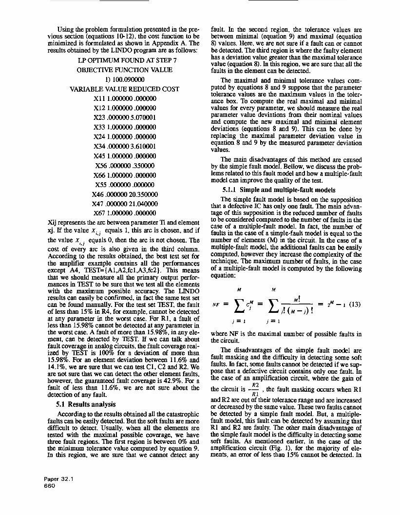
Using the problem formulation presented in the pre- vious section (equations 1@12), the cost function to be minimized is formulated as shown in Appendix A. The results obtained by the LINDO program are as follows:
LP OPTIMUM FOUND AT STEP 7 OBJECTIVE FUNCTION VALUE
1) 100.09oooO VARIABLE VALUE REDUCED COST
x111.000000.000000 x12 1.000000.000000 X23.000000 5.070001 x33 1.000000.000000 X24 1.000000.000000 X34.000000 3.610001 x45 1.000000 .m X56.000000.35oooO x66 1.000000.000000 x55.000000 .000000
X46.000000 20.35oooO x47.000000 21.04oooO X67 1.000000.000000
Xij represents the arc between parameter Ti and element xj. If the value equals 1, this arc is chosen, and if the value xI, equals 0, then the arc is not chosen. The cost of every arc is also given in the third column. According to the results obtained, the best test set for the amplifier example contains all the performances except A4, TEST={Al,A2,fcl,A3,fc2}. This means that we should measure all the primary output perfor- mances in TEST to be sure that we test all the elements with the maximum possible accuracy. The LINDO results can easily be confirmed, in fact the same test set can be found manually. For the test set TEST, the fault of less than 15% in R4, for example, cannot be detected at any parameter in the worst case. For R1, a fault of less than 15.98% cannot be detected at any parameter in the worst case. A fault of more than 15.98%, in any ele- ment, can be detected by TEST. If we can talk about fault coverage in analog circuits, the fault coverage real- ized by TEST is 100% for a deviation of more than 15.98%. For an element deviation between 11.6% and 14.1%, we are sure that we can test C1, C2 and R2. We are not sure that we can detect the other element faults, however, the guaranteed fault coverage is 42.9%. For a fault of less than 11.6%. we are not sure about the detection of any fault.
5.1 Results analysis According to the results obtained all the catastrophic
faults can be easily detected. But the soft faults are more difficult to detect. Usually, when all the elements are tested with the maximal possible coverage. we have three fault regions. The first region is between 0% and the minimum tolerance value computed by equation 9. In this region, we are sure that we cannot detect any
fault. In the second region, the tolerance values are between minimal (equation 9) and maximal (equation 8) values. Here, we are not sure if a fault can or cannot be detected. The third region is where the faulty element has a deviation value greater than the maximal tolerance value (equation 8). In this region, we are sure that all the faults in the element can be detected.
The maximal and minimal tolerance values com- puted by equations 8 and 9 suppose that the parameter tolerance values are the maximum values in the toler- ance box. To compute the real maximal and minimal values for every parameter, we should measure the real parameter value deviations fiom their nominal values and compute the new maximal and minimal element deviations (equations 8 and 9). This can be done by replacing the maximal parameter deviation value in equation 8 and 9 by the measured parameter deviation values.
The main disadvantages of this method are caused by the simple fault model. Bellow, we discuss the prob- lems related to this fault model and how a multiple-fault model can improve the quality of the test.
5.1.1 Simple and multiple-fault models The simple fault model is based on the supposition
that a defective IC has only one fault. The main advan- tage of this supposition is the reduced number of faults to be considered compared to the number of faults in the case of a multiple-fault model. In fact, the number of faults in the case of a simple-fault model is equal to the number of elements (M) in the circuit. In the case of a multiple-fault model. the additional faults can be easily computed, however they increase the complexity of the technique. The maximum number of faults. in the case of a multiple-fault model is computed by the following equation:
M M
M! 2M - 1 (13)
J = 1 j = 1
where NF is the maximal number of possible faults in the circuit.
The disadvantages of the simple fault model are fault masking and the difficulty in detecting some soft faults. In fact, some faults cannot be detected if we sup- pose that a defective circuit contains only one fault. In the case of an amplification circuit, where the gain of the circuit is -- , the fault masking occurs when R1 and R2 are out of their tolerance range and are increased or decreased by the same value. These two faults cannot be detected by a simple fault model. But, a multiple- fault model, this fault can be detected by assuming that R1 and R2 are faulty. The other main disadvantage of the simple fault model is the difficulty in detecting some soft faults. As mentioned earlier, in the case of the amplification circuit (Fig. 1). for the majority of ele- ments, an error of less than 15% cannot be detected. In
R2 R1
Paper 32.1 660

some cases, the gap between maximal and minimal ele- ment deviations (equations 8 and 9) is too large. To solve this problem, we should consider the multiple- fault model. In fact, when all the possible faults are con- sidered to occur. circuit testing is transformed into a diagnostic problem [l], [23. In this case the gap between maximal and minimal element deviations is zero. since we have only one element deviation. If the simple fault model is changed to a double-fault model, the gap will decrease. and so on until 0 is reached in the diagnostic case.
6.0 Conclusion In this paper, an analog circuit testing method is pre-
sented. This method uses a new circuit modeling tech- nique based on the sensitivity computation and on graph theory. The efficiency of test vector generation for sim- ple faults in analog circuits is shown. Also, with sensi- tivity testing, we can easily estimate the testability of analog circuits and modify the circuit in order to increase its testability. Using the testing approach pre- sented, appropriate tests are identified for testing cata- strophic and soft faults.
In future work, we will try to reduce the number of parameters to be measured without affecting test qual- ity. In some cases, the best test can be costly. This hap- pens when the best test set contains all the parameters. To solve this problem, we need to solve an optimization problem designed to cover a l l the elements with the minimum cost and minimum number of parameters. The other part of this work will involve hierarchical test “vector” generation for analog circuits.
Aknowledgement The authors wish to think Samir Lejmi for his sup-
port in the mathematical formulation of the problem.
r 11
[21
[31
References Mustapha Slamani and Bozena Kaminska, “Analog Circuit Fault Diagnosis Based on Sensitivity Com- putation and Fault Testing”, IEEE Design and Test of Computers, March 1992, pp. 30-39 Mustapha Slamani and Bozena Kaminska. ‘‘Testing Analog Circuits by Sensitivity Computation”, European Design Automation Conference, Paris, Feb. 1992. pp. 532-537. A. L. Rosenblum, and M. S . Ghaussi, “Multiparam- eter Sensitivity Problem in Active RC Networks,” IEEE Trans. Circuit Theory, Vol. CT-18, No. 6 Nov. 1971, pp. 592-599.
[41 W. J. Butler and S . S. Haykin. “Multiparameter Sen- sitivity Problems in Network Theory”, Proc. Insti- tute of Electrical Engineers, Vol 117, No.12, Dec.
[5] J. K. Fidler, “Differential-Incremental-Sensitivity Relationships,” Electronics Letters, Vol. 20, No. 10, May 1984, pp. 626-627.
[6] Erich Wehrhahn. “Hierarchical Circuit Analysis.” Roc. ISCAS. May 1989, pp. 701-704.
[71 P. Duhamel and J.C. Rault, “Automatic Test Genera- tion Techniques for Analog Circuits and Systems: A
1970, pp 2228-2236.
Review, “ IEEE Trans. Circuits and Systems, Vol.
[SI L. Milor and V. Visavanathan, “Detection of Cata- strophic Faults in Analog Circuits,” IEEE Trans. Computer Aided Design, Vol. CAD-8, No. 2, Feb.
[9] K.R. Chin, “Functional Testing of Circuits and SMD Bords with Limited Nodal Access,” Int’l Test Conf. IEEE CS Press, Los Alamitos, Calif., pp. 129-143.
[lo] H. Dai and M. Sounders, “Time-Domain Testing Strategies and Fault Diagnosis for Analog Sys- tems, “ IEE Trans. Instru. and Meas., Vo1.39, No.1, Feb. 1990, pp.157-162.
1111 P.P. Fasang, D. Mullins, and T. Wong, “Design for Testability for Mixed Analoe/Dinital ASICs.”
CAS-26, NO. 7. July 1979, pp. 41 1-439.
1989, pp.114-130.
Roc. IEEE Custom Integratd C%cuits Conf..
E.A. Sloan, “Transfer Function Estimation, Partl, Theoretical and Practical Considerations,” Proc. Int’l Test Conf., IEEE CS press, 1984, pp. 426- 439. L. Milor and V.A. Sangiovanni, “Optimal Test Set Design for Analog Circuits,” Roc. Int’l Test Conf.. IEEE CS press, 1990, pp.294-297. A. Mckeon and A. Wakeling, “Fault Diagnosis in Analog Circuits Using AI Techniques”, Proc. Int’l Test Conf., 1989, pp. 118-123. M. Soma “ A Design-for-Test Methodology for Active Analog Filters”, Proc. Int’l Test Conf.,
HSPICE User’s Manual: H8801, Meta-Software, Inc., 1988. LINDO User’s Manual, “Linear, and Quadratic Programming with LINDO,” Linus Schrage. Fourth Edition.
1988, pp. 16.5.1-16.5.4
1990, pp. 183-192.
APPENDIX A min 15.98 x l l + 14.1 x12 + 20.27 X23 + 15.2 x33 + 11.2 x24 + 14.81 x34 + 15 x45 + 15 x56 + 14.65 x66 + 15 x55 + 35 x46 + 35 x47 + 13.96 x67 st x12 >= 0 x l l = 1 x23 >= 0 xlz-1 x24>=0 x23 + x33 = 1 x33 >= 0 x24+x34= 1 x34 >= 0 x45 + x55 = 1 x45 >= 0 x46+x56+x66=1 x46 >= 0 x47 + x67 = 1 x47 >= 0 x l l + x12 <= 2 x55 >= 0 x23 + x24 <= 2 x56 >= 0 x33 + x34 <= 2 x66 >= 0 x45 + x46 + x47 <= 3 x67 >= 0 x66 + x67 <= 2 end x55 + x56 <= 2 leave x l l >= 0
Paper 32.1 661
Copyright © 2022 FDOKUMEN