On-Line Global Energy Optimization in Multi-Core Systems Using Principles of Analog Computation
14
IEEE JOURNAL OF SOLID-STATE CIRCUITS, VOL. 42, NO. 7, JULY 2007 1593 On-Line Global Energy Optimization in Multi-Core Systems Using Principles of Analog Computation Zeynep Toprak Deniz, Member, IEEE, Yusuf Leblebici, Senior Member, IEEE, and Eric A. Vittoz, Life Fellow, IEEE Abstract—This work presents the design and the silicon im- plementation of an on-line energy optimizer unit based on novel analog computation approaches, which is capable of dynamically adjusting power supply voltages and operating frequencies of multiple processing elements on-chip. The optimized voltage/fre- quency assignments are tailored to the instantaneous workload information on multiple tasks and fully adaptive to variations in process and temperature. The optimizer unit has a response time of less than 50 s, occupies a silicon area of 0.021 mm task and dissipates 2 mW/task. Index Terms—Analog computation, dynamic voltage and frequency scaling, energy management, on-line energy optimiza- tion, pseudo-resistors, System-on-Chip, translinear loops, weak inversion. I. INTRODUCTION D UE to recent developments in the embedded systems technologies, multi-core System-on-Chip (SoC) and Network-on-Chip (NoC) architectures are becoming virtually ubiquitous. Such systems are widely used in many wireless applications such as mobile computing, where the available energy is fundamentally limited [1]. In multi-processing element (PE) systems, due to the diver- sity of the applications that run within the system and their dif- ferent degrees of parallelism, the workloads imposed on the system components are non-uniform over time. This introduces slack times during which the system can reduce its performance to save energy. The key to energy-efficient designs is the ability to tune PE performance to the non-uniform workload [2]–[4]. In cases where performance requirements of a component vary significantly during the active operation regime, dynamic voltage scaling (DVS) is the preferred approach for reducing the overall energy dissipation. DVS exploits the fact that the peak operating frequency of a processing element is propor- tional to the supply voltage, while the amount of dynamic en- ergy required for a given workload is proportional to the square of the PE’s supply voltage [5]. In applications such as MPEG-2 video encoding/decoding where instantaneous workload vari- ations in the order of 1:10 have been reported between con- secutive frames (every 33 ms) [6], [7], DVS typically results in substantial energy savings. The varying workload of a given Manuscript received November 17, 2006; revised February 16, 2007. Z. Toprak Deniz was with the Ecole Polytechnique Fédérale de Lausanne (EPFL), Lausanne CH-1015, Switzerland. She is now with IBM Thomas J. Watson Research Center, Yorktown Heights, NY 10598 USA (e-mail: ztoprak@ us.ibm.com). Y. Leblebici and E. A. Vittoz are with the Ecole Polytechnique Fédérale de Lausanne (EPFL), Lausanne CH-1015, Switzerland (e-mail: yusuf.leblebici@ epfl.ch; eric.vittoz@epfl.ch). Digital Object Identifier 10.1109/JSSC.2007.896694 Fig. 1. (a) Mapping of MPEG-2 into a 4 core SoC. (b) Actual (dark) and esti- mated (light grey) workload of the frames of an MPEG-2 test sequence. Fig. 2. Block diagram representation of the proposed on-line global energy management unit. application (e.g., user’s request or the computational task to be carried out) provides an opportunity to tune the performance (speed) of the system. Each task of the given application re- quires a finite number of clock cycles ( ,a dimensionless vari- able representing the workload) to be executed, depending on the PE on which they are mapped. Non-stationary workload of an application is predicted based on stochastic models, which use distributions to describe the times of user request arrivals, and time it takes for state transitions for a device to service a user request. In these approaches, it is assumed that the system and the workload can be modeled by Markov chains [8], [9]. To serve as a motivational example, Fig. 1(a) shows a four- core implementation of MPEG-2 video decoding where the al- gorithm is decomposed into a set of parallel tasks communi- cating over a general-purpose data network and mapped onto a SoC consisting of four processing elements [10]. In [6], the au- thors derive Hidden Markov Models (HMM) for the workload characterization of specific tasks as shown in Fig. 1(b). It can be seen that the estimated workload characteristics (light grey) closely follow the actual (dark) workload characteristics, and 0018-9200/$25.00 © 2007 IEEE
-
Upload
independent -
Category
Documents
-
view
2 -
download
0
Transcript of On-Line Global Energy Optimization in Multi-Core Systems Using Principles of Analog Computation

IEEE JOURNAL OF SOLID-STATE CIRCUITS, VOL. 42, NO. 7, JULY 2007 1593
On-Line Global Energy Optimization in Multi-CoreSystems Using Principles of Analog Computation
Zeynep Toprak Deniz, Member, IEEE, Yusuf Leblebici, Senior Member, IEEE, and Eric A. Vittoz, Life Fellow, IEEE
Abstract—This work presents the design and the silicon im-plementation of an on-line energy optimizer unit based on novelanalog computation approaches, which is capable of dynamicallyadjusting power supply voltages and operating frequencies ofmultiple processing elements on-chip. The optimized voltage/fre-quency assignments are tailored to the instantaneous workloadinformation on multiple tasks and fully adaptive to variations inprocess and temperature. The optimizer unit has a response timeof less than 50 s, occupies a silicon area of 0.021 mm2 task anddissipates 2 mW/task.
Index Terms—Analog computation, dynamic voltage andfrequency scaling, energy management, on-line energy optimiza-tion, pseudo-resistors, System-on-Chip, translinear loops, weakinversion.
I. INTRODUCTION
DUE to recent developments in the embedded systemstechnologies, multi-core System-on-Chip (SoC) and
Network-on-Chip (NoC) architectures are becoming virtuallyubiquitous. Such systems are widely used in many wirelessapplications such as mobile computing, where the availableenergy is fundamentally limited [1].
In multi-processing element (PE) systems, due to the diver-sity of the applications that run within the system and their dif-ferent degrees of parallelism, the workloads imposed on thesystem components are non-uniform over time. This introducesslack times during which the system can reduce its performanceto save energy. The key to energy-efficient designs is the abilityto tune PE performance to the non-uniform workload [2]–[4].
In cases where performance requirements of a componentvary significantly during the active operation regime, dynamicvoltage scaling (DVS) is the preferred approach for reducingthe overall energy dissipation. DVS exploits the fact that thepeak operating frequency of a processing element is propor-tional to the supply voltage, while the amount of dynamic en-ergy required for a given workload is proportional to the squareof the PE’s supply voltage [5]. In applications such as MPEG-2video encoding/decoding where instantaneous workload vari-ations in the order of 1:10 have been reported between con-secutive frames (every 33 ms) [6], [7], DVS typically resultsin substantial energy savings. The varying workload of a given
Manuscript received November 17, 2006; revised February 16, 2007.Z. Toprak Deniz was with the Ecole Polytechnique Fédérale de Lausanne
(EPFL), Lausanne CH-1015, Switzerland. She is now with IBM Thomas J.Watson Research Center, Yorktown Heights, NY 10598 USA (e-mail: [email protected]).
Y. Leblebici and E. A. Vittoz are with the Ecole Polytechnique Fédérale deLausanne (EPFL), Lausanne CH-1015, Switzerland (e-mail: [email protected]; [email protected]).
Digital Object Identifier 10.1109/JSSC.2007.896694
Fig. 1. (a) Mapping of MPEG-2 into a 4 core SoC. (b) Actual (dark) and esti-mated (light grey) workload of the frames of an MPEG-2 test sequence.
Fig. 2. Block diagram representation of the proposed on-line global energymanagement unit.
application (e.g., user’s request or the computational task to becarried out) provides an opportunity to tune the performance(speed) of the system. Each task of the given application re-quires a finite number of clock cycles ( , a dimensionless vari-able representing the workload) to be executed, depending onthe PE on which they are mapped. Non-stationary workload ofan application is predicted based on stochastic models, whichuse distributions to describe the times of user request arrivals,and time it takes for state transitions for a device to service auser request. In these approaches, it is assumed that the systemand the workload can be modeled by Markov chains [8], [9].
To serve as a motivational example, Fig. 1(a) shows a four-core implementation of MPEG-2 video decoding where the al-gorithm is decomposed into a set of parallel tasks communi-cating over a general-purpose data network and mapped onto aSoC consisting of four processing elements [10]. In [6], the au-thors derive Hidden Markov Models (HMM) for the workloadcharacterization of specific tasks as shown in Fig. 1(b). It canbe seen that the estimated workload characteristics (light grey)closely follow the actual (dark) workload characteristics, and
0018-9200/$25.00 © 2007 IEEE

1594 IEEE JOURNAL OF SOLID-STATE CIRCUITS, VOL. 42, NO. 7, JULY 2007
Fig. 3. (a) Task graph of five tasks mapped on two processing elements, and (b) the resistive network equivalent of the given TG.
that the frame-to-frame variations in the workload may be ashigh as a factor of 10. This observation also reinforces the casefor fine-grained DVS to be performed on all PEs in order to min-imize energy dissipation, based on instantaneous workload.
DVS is based on reducing the performance level of the com-ponent during periods of low utilization so that the task is alwayscompleted just-in-time, consuming minimum energy [11], [12].While the local energy dissipation of each PE can be minimizedusing DVS techniques based on workload predictions, it can beshown that these local minima usually do not represent the globalenergy minimum, which can only be reached by considering therelative timing dependencies of all tasks running in the system.This problem of minimizing the overall dissipated energy in amulti-PE system under timing constraints and subject to DVS,has already been formulated in a rigorous fashion, yet a compact.real-time implementation has not been offered [13]–[15]
Our approach demonstrates the solution to the problem of on-line optimization of the dissipated energy in multi-PE systemswith interrelated tasks under timing constraints using the basicprinciples of analog computation by converging on the globalminima of the constrained optimization problem which are rep-resented as stable operating points of a simple resistive network(RN). The input set of the circuit consists of individual work-load estimates for each task and for each PE, while the outputconsists of assigned supply voltage/frequency values for eachPE as well as the allocated time duration for each task as illus-trated in Fig. 2.
The remainder of this paper is organized as follows. InSections II and III, we concentrate on demonstrating an on-line solution to complex multi-variable energy optimizationproblem. Implementation of main building blocks is given inSection IV. Configurability of pseudo-resistor array is discussedin Section V. The closed-loop operation principle of the proposedanalog optimizer block is described in Section VI. In Section VII,experimental results is discussed in comparison with the simu-lation results. Conclusions are provided in Section VIII.
II. FROM TASK GRAPH TO RESISTIVE NETWORK
The authors have previously demonstrated the analogybetween the problem of minimizing energy consumption on
a complex system under timing constraints, and the problemof minimizing power dissipation in a resistive network underKirchoff’s Current Law (KCL) constraints [16]. Accordingto Maxwell’s Heat theorem the RN will consume the lowestpossible power , at steady-state for a given drivingcurrent [17]. The equivalence between the two analogous mini-mization problems is summarized in (1) and (2), given in Fig. 3.Here, individual tasks are modeled with device conductances
, controlled by the ratio where is the averagepower consumption of the PE during task , and is the taskduration. For a detailed explanation of this analogy, refer toAppendix A.
Consider the example illustrated in Fig. 3(a), where five tasksare mapped and scheduled on two PEs. The total dissipated en-ergy in the system can be written as the summation of all thetask energies (1). Since each task requires a given number
of cycles, and each cycle consumes an amount of energy,this amount can be reduced if the supply voltage of thePE is reduced under the cost of cycle time increase. Theformal algorithmic solution of (1) is certainly possible in realtime, yet the computational overhead that is needed may be-come prohibitive especially when taking into account realistictiming/delay models and secondary effects such as leakage dis-sipation. Fig. 3(b) shows the equivalent RN of the given taskgraph (TG), in which duration of each task correspondsto the current in a resistor . The TG period T corresponds tothe total current driving the circuit. Due to KCL, will besplit into parallel branch currents that are inversely proportionalto branch resistances. Hence, it can be seen that the simple RNactually realizes the solution to the dissipated power minimiza-tion problem for a given driving current under KCL constraints(2). It is important to emphasize that the mapping of a given TGto its equivalent RN is based on converting the time domain re-lation between tasks into equivalent RN currents. Hence, we donot consider this procedure to be equivalent to finding the dualof a given TG.
The overall block diagram of the intended system is given inFig. 4, where the only input (task workloads— ) to the pro-posed optimizer block is highlighted in grey and the outputs ofthe optimizer block to the SoC/NoC architecture (the supply
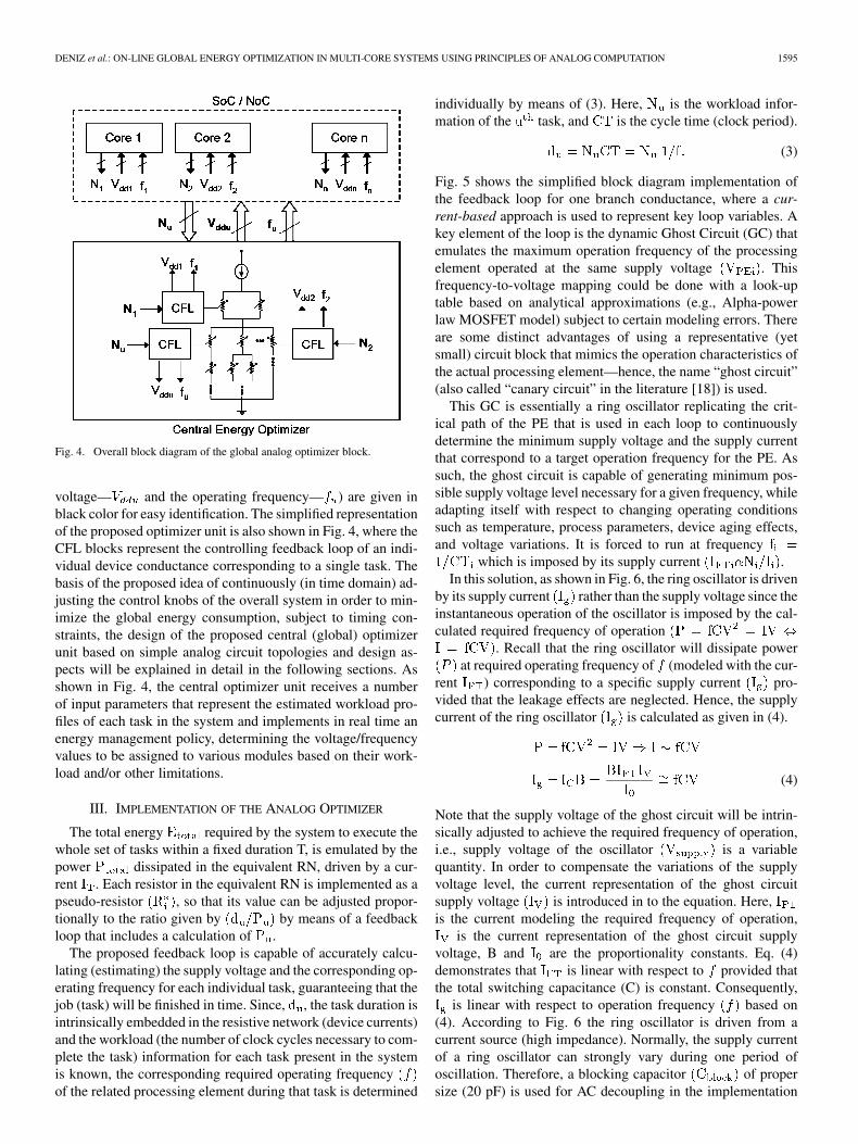
DENIZ et al.: ON-LINE GLOBAL ENERGY OPTIMIZATION IN MULTI-CORE SYSTEMS USING PRINCIPLES OF ANALOG COMPUTATION 1595
Fig. 4. Overall block diagram of the global analog optimizer block.
voltage— and the operating frequency— ) are given inblack color for easy identification. The simplified representationof the proposed optimizer unit is also shown in Fig. 4, where theCFL blocks represent the controlling feedback loop of an indi-vidual device conductance corresponding to a single task. Thebasis of the proposed idea of continuously (in time domain) ad-justing the control knobs of the overall system in order to min-imize the global energy consumption, subject to timing con-straints, the design of the proposed central (global) optimizerunit based on simple analog circuit topologies and design as-pects will be explained in detail in the following sections. Asshown in Fig. 4, the central optimizer unit receives a numberof input parameters that represent the estimated workload pro-files of each task in the system and implements in real time anenergy management policy, determining the voltage/frequencyvalues to be assigned to various modules based on their work-load and/or other limitations.
III. IMPLEMENTATION OF THE ANALOG OPTIMIZER
The total energy required by the system to execute thewhole set of tasks within a fixed duration T, is emulated by thepower dissipated in the equivalent RN, driven by a cur-rent . Each resistor in the equivalent RN is implemented as apseudo-resistor , so that its value can be adjusted propor-tionally to the ratio given by by means of a feedbackloop that includes a calculation of .
The proposed feedback loop is capable of accurately calcu-lating (estimating) the supply voltage and the corresponding op-erating frequency for each individual task, guaranteeing that thejob (task) will be finished in time. Since, , the task duration isintrinsically embedded in the resistive network (device currents)and the workload (the number of clock cycles necessary to com-plete the task) information for each task present in the systemis known, the corresponding required operating frequencyof the related processing element during that task is determined
individually by means of (3). Here, is the workload infor-mation of the task, and is the cycle time (clock period).
(3)
Fig. 5 shows the simplified block diagram implementation ofthe feedback loop for one branch conductance, where a cur-rent-based approach is used to represent key loop variables. Akey element of the loop is the dynamic Ghost Circuit (GC) thatemulates the maximum operation frequency of the processingelement operated at the same supply voltage . Thisfrequency-to-voltage mapping could be done with a look-uptable based on analytical approximations (e.g., Alpha-powerlaw MOSFET model) subject to certain modeling errors. Thereare some distinct advantages of using a representative (yetsmall) circuit block that mimics the operation characteristics ofthe actual processing element—hence, the name “ghost circuit”(also called “canary circuit” in the literature [18]) is used.
This GC is essentially a ring oscillator replicating the crit-ical path of the PE that is used in each loop to continuouslydetermine the minimum supply voltage and the supply currentthat correspond to a target operation frequency for the PE. Assuch, the ghost circuit is capable of generating minimum pos-sible supply voltage level necessary for a given frequency, whileadapting itself with respect to changing operating conditionssuch as temperature, process parameters, device aging effects,and voltage variations. It is forced to run at frequency
which is imposed by its supply current .In this solution, as shown in Fig. 6, the ring oscillator is driven
by its supply current rather than the supply voltage since theinstantaneous operation of the oscillator is imposed by the cal-culated required frequency of operation
. Recall that the ring oscillator will dissipate powerat required operating frequency of (modeled with the cur-
rent ) corresponding to a specific supply current pro-vided that the leakage effects are neglected. Hence, the supplycurrent of the ring oscillator is calculated as given in (4).
(4)
Note that the supply voltage of the ghost circuit will be intrin-sically adjusted to achieve the required frequency of operation,i.e., supply voltage of the oscillator is a variablequantity. In order to compensate the variations of the supplyvoltage level, the current representation of the ghost circuitsupply voltage is introduced in to the equation. Here,is the current modeling the required frequency of operation,
is the current representation of the ghost circuit supplyvoltage, B and are the proportionality constants. Eq. (4)demonstrates that is linear with respect to provided thatthe total switching capacitance (C) is constant. Consequently,
is linear with respect to operation frequency based on(4). According to Fig. 6 the ring oscillator is driven from acurrent source (high impedance). Normally, the supply currentof a ring oscillator can strongly vary during one period ofoscillation. Therefore, a blocking capacitor of propersize (20 pF) is used for AC decoupling in the implementation

1596 IEEE JOURNAL OF SOLID-STATE CIRCUITS, VOL. 42, NO. 7, JULY 2007
Fig. 5. Block diagram implementation of the optimization feedback loop.
Fig. 6. Implementation of the ghost circuit and the corresponding power cal-culation loop.
which provides low impedance at the frequency of operation(refer to Fig. 6).
The predicted workload information is injected into eachloop in the form of a 4-bit external control variable. Any changein influences the current corresponding to the target operationfrequency in the feedback loop. Hence, the simple GCdetermines the supply voltage level to be applied to the PE forachieving the target frequency as well as the resulting dynamiccurrent consumption . The voltage and the frequencyare transmitted to the PE. They are also converted to current rep-resentations and in order to calculate the pseudo-resistorcontrolling currents .
An alternative look-up table approach would have requiredthe characterization of the core for throughput at a given clockspeed and at a given voltage, where ample margins must be al-lowed for temperature, power supply and fabrication variationswhich requires an extensive effort to build a hard-coded speedversus supply table. The implementation of the ghost circuit inthe control path effectively eliminates the need for such mod-eling that is inherently prone to inaccuracies. The amount ofcurrent that will be drawn from the supply rail of the oscillatorwill follow the variations in the frequency, and hence, of thesupply voltage level. Also, the short circuit current characteris-tics of logic gates constructing the processing element is imi-tated accurately at first approximation, based on the expectationthat the processing element is designed appropriately; i.e., the
transitions and the waveforms during transitions at in/output ofthe internal CMOS gates are homogeneous. Since, the transi-tions in the ghost circuit are homogeneous; short circuit powerconsumption of the processing element is modeled by the im-plemented ghost circuit.
IV. IMPLEMENTATION OF THE MAIN BUILDING BLOCKS
Current-mode processing in each feedback loop is carried outby single quadrant current multiplier/dividers labeled as .Each current operator is implemented by the simple alternatingtopology translinear loop (TLL) of four transistors operated inweak inversion with their bulks connected to the common sub-strate as shown in Fig. 7. Here, a clockwise element (CW) is theone whose gate-to-source voltage is a voltage drop in the clock-wise direction of the loop. So we shall consider a counterclock-wise element (CCW) as the one whose gate-to-source voltage isa voltage increase in the clockwise direction of the loop. Recallthat the channel current, , of a saturated MOS transistor, oper-ating in weak inversion regime, is given by (7), where , ,and are the gate-to, source-to and drain-to bulk potentialsrespectively. is given by (5), where is the specific current[given in (6)], is the slope factor [it can be interpreted as the(incremental) capacitive divider ratio between the gate and thechannel potential], is the threshold voltage for a channel atequilibrium, and is the thermal voltage, [19]–[21].
(5)
(6)
The given loop has an alternating topology; that is, we alternatebetween CW and CCW elements, as we go around the loop. Ap-plying the Kirchhoff’s voltage law and using voltage-translinearprinciple around the loop illustrated in Fig. 7 results in (8). Byintroducing (7) into (8) for all loop transistors (divided by ,that is common to all transistors), and exponentiating both sidesof the equation yields in (9) if all transistors are identical. Theprecision of the translinear loop is degraded by mismatch

DENIZ et al.: ON-LINE GLOBAL ENERGY OPTIMIZATION IN MULTI-CORE SYSTEMS USING PRINCIPLES OF ANALOG COMPUTATION 1597
Fig. 7. A subthreshold MOS translinear loop consisting of two CW transistorsand two CCW transistors, constructed to operate as an inverse current multiplier.
which is equivalent to the relative errors of propor-tional to .
(7)
(8)
(9)
This is a single quadrant current multiplier/divider, thus allcurrents should be positive. Hence, we can take the inverse of acurrent with respect to a unit current, provided that all currentsentering/leaving the TLL are positive. It should be noted thatcurrent mirrors of necessary type (PMOS and/or NMOS) areused whenever needed to drive the TLLs in the feedback loops.The current mirrors are excluded from Fig. 7 for the sake ofsimplicity. Such multiplier/divider schemes are utilized in thefeedback loop to implement the analog optimizer for convertingduration (time) to frequency (where all variables are representedas currents) and to implement the pseudo-resistor controllingcurrent definition by means of ratio of current multiplications.
The simulation results of the implemented single quadrantcurrent multiplier/divider are given in Fig. 8, for different cur-rent levels, , , and being the three current inputs, wherethe block functionality is given in (9) as . TheTLL calculates the inverse of the current appearing in thedenominator of the function. Here, current is constant andequal to 1 A for all curves in the figure. In Fig. 8, the ideallinear output current is also provided for A level, forcomparison. The linearity of the translinear loop degrades fromideal as the current levels increase.
Each pseudo-resistor in the resistive network is realized asa single MOS transistor operating in weak inversion where theequivalent conductance value of each transistor is controlledindependently by a current by means of a control transistor(Fig. 9)—thus, utilizing only a few transistors.
For a given value of , a transistor is in weak inversion ifboth and are large enough to obtain atboth ends of its channel. This condition is equivalent to ensuring
Fig. 8. Simulated linearity of the translinear loop for possible different currentlevels.
Fig. 9. Implementation of pseudo-resistors in a CMOS process.
Fig. 10. Implementation of grounded resistors in pseudo-resistive network.
a value of its saturation current that is much smaller than itsspecific current, . Recall that the channel current of a MOStransistor operated in weak inversion can be written as givenin (10):
where
(10)
By defining a pseudo-voltage (independent of ) givenby (11):
for p-channel for n-channel (11)
where is an arbitrary positive scaling voltage [21], [22], andthe channel potential, the channel current of the MOS device
can be rewritten as:
(12)
which corresponds to a linear pseudo-Ohm’s law. The pseudo-voltage is always negative for an n-channel transistor (positivefor a p-channel), and tends to 0 for large values of V. Thus, the

1598 IEEE JOURNAL OF SOLID-STATE CIRCUITS, VOL. 42, NO. 7, JULY 2007
Fig. 11. (a) Resistive network representation of the arbitrary task graph, and (b) duplicated parallel branch with its own bias current.
pseudo-ground 0 (0-reference for pseudo-voltage ) is ob-tained by imposing large enough to make sure that the tran-sistor is saturated. Pseudo-conductance which is control-lable by , and thus, pseudo-resistance can be definedas in (13) in weak inversion operation.
(13)
In such systems, the linear pseudo-Ohm’s law is valid, i.e.,a network of transistors remains linear with respect to currents,and the pseudo-resistance, of each transistor is controllable in-dependently by the value of its gate voltage. Conductance ofeach pseudo-resistor may alternatively be controlled by a cur-rent by means of a control transistor, as shown in Fig. 9. In thissolution, all transistors must share the same substrate and thereference voltage is common to all the control transistorsof the network and selected to ensure weak inversion in all pos-sible situations. The mapping of resistive-networks into its tran-sistor-based equivalents on the basis of pseudo-Ohm’s law canbe generalized: any arbitrary network of linear resistors can beimplemented by replacing each resistor by a transistor ,with all the transistors in the same substrate [22]–[24].
A resistor connected to ground potential in the resistive-net-work corresponds to a saturated MOS transistor (operated inweak inversion) that provides a pseudo-ground (0 ) in the equiv-alent pseudo-resistive network (refer to Fig. 10). Any currentflowing to the pseudo-ground can be easily extracted without in-fluencing the branch current ratio, by means of a grounded cur-rent mirror made of transistors complementary to those of thenetwork as shown in Fig. 10 [16]–[18]. Hence, grounded cur-rent-mirrors are used to sense each branch current separately,to be further used in the feedback loop, which is presented inFig. 5.
This solution could become problematic when we considerthe mapping of more complex task graphs into their equivalentresistive networks. An example resistive network mapping isgiven in Fig. 11(a) corresponding to an arbitrary task graph.In order to measure the branch currents and , we shouldduplicate the parallel branch consisting of and and biasthis copy with , which is the current flowing throughthe main parallel branch as in Fig. 11(b). Since now, there aretwo currents flowing towards ground we can easily measure thebranches currents individually, by means of grounded current-mirrors.
Fig. 12. (a) Schematic representation and (b) the input-output characteristicsof the implemented maximum current selector.
The result of current mode processing in each loop is the cur-rent (14) that drives (controls) the corresponding pseudo-re-sistor as illustrated in Fig. 5. The factor introduced byis proportional to the equivalent switching capacitor, that may bedifferent for different processing elements. Here, representsthe modeled static current consumption of the PE (proportionalto the total number of gates), with a static GC which is added tothe loop. This current is added to the dynamic current consump-tion , resulting in (14).
(14)
Consequently, the corresponding device conductance valuechanges according to (14). This change in the value of de-vice conductance forces all the branch currents in the RN to be

DENIZ et al.: ON-LINE GLOBAL ENERGY OPTIMIZATION IN MULTI-CORE SYSTEMS USING PRINCIPLES OF ANALOG COMPUTATION 1599
Fig. 13. Modular system approach supporting different task graphs topologies.
adjusted by means of KCL. As the system settles to its new op-erating point, the new device currents in the pseudo-RN are de-termined by KCL, dictating the optimum task duration with theprescribed supply voltage and operating frequency for each PEand for each task to minimize system-wide energy dissipation.Detailed simulation results of the implemented pseudo-resistivenetwork can be found in [25].
Minimum current limiter (Maximum current selector) blocksare used to restrict the operation range to a defined value. Theupper limit of the operation is intrinsically limited by the tech-nology due to the fact that the maximum allowed core oper-ating voltage is fixed to a constant level. In order to guaranteethat the lower limit of operation, which is 1.2 V or 150 MHz isnot violated under any circumstances two minimum current lim-iter blocks are used in all the feedback loops. For this purposea combination of nMOS transistors is used to carry out addi-tion/subtraction of the replicas of the input currents as given inFig. 12(a). The figure also shows the simulation results of theblock. Note that the output current follows the higher of the twoinput currents.
V. CONFIGURABLE PSEUDO-RESISTOR ARRAY
Typically, a large number of diverse applications can bemapped and run on high-performance distributed embeddedsystems (SoC/NoC). Hence, the proposed circuit architectureshould be built with a modular approach to support differentsoftware applications as opposed to a hardwired circuit solu-tion. This capability of a modular architecture can be exploitedby implementing an array of pseudo-resistors with corre-sponding control feedback loops (CFL) and various numberof necessary type of current mirrors to pick up the branchcurrents at pseudo-ground nodes of the RN as shown in Fig. 13.In addition to these modular building blocks several constantcurrent sources can be implemented to model various taskgraph periods. It should be noted that the switching network isnot shown in the figure for the sake of simplicity. Consequently,the implemented array of pseudo-resistors can be easily ex-panded to support any arbitrary TG that can be mapped onthe given system of PEs. Recall that device currents model
the corresponding task durations. Hence, each device currentshould be picked up and fed back to the related CFL. Besides,extracting currents flowing to the pseudo-ground is preferred inorder not to influence the branch currents. Hence, it is favoredto configure the RN in such a way that in any constructedarchitecture the maximum number of parallel branch currentsflow to the pseudo-ground nodes of the RN.
A simple example of such a modular configuration, basedon built in pseudo-resistor array, is shown in Fig. 14(b) for theTG of Fig. 14(a). Here, the connections necessary for the givenconfiguration are indicated as dashed lines and for the sake ofeasy identification only the necessary sub-blocks used for thegiven configuration are shown. In the given TG, on the firstPE is executed in parallel to sequential tasks , , and onthe second PE. Therefore, as a consequence of parallelism, theavailable time will be split among , , and tailored totheir instantaneous workload, where can be executed duringthe task graph period . Consequently, the pseudo-resistorsmodeling the tasks mapped on the second PE are connectedin parallel and the resulting RN is connected in series to thepseudo-resistor modeling the first task as shown in Fig. 14(b).Note that the parallel section of the equivalent RN is connectedto the pseudo-ground node.
VI. CLOSED-LOOP OPERATION OF THE OPTIMIZER
After showing how the feedback loop is implemented andhow the proposed optimizer block can be made configurable, itis now necessary to show how the network of controlled resistorsoperates for a given set of workload requirements. It is importantto highlight that the feedback loop responsible for updating each
value operates in continuous time (based on GC response),rather than in a discrete-time iteration. The stability behaviorof the feedback loops taking into account the coupling betweenloops through the RN has been thoroughly analyzed (refer toAppendix B). It was shown that the dynamic behavior of eachresistive element control loop is governed by a single-domi-nant-pole transfer function. Therefore, as also shown analyti-cally, the entire system always converges to a stable and uniqueoperating point for a given set of workloads. Also, note that the

1600 IEEE JOURNAL OF SOLID-STATE CIRCUITS, VOL. 42, NO. 7, JULY 2007
Fig. 14. (a) Task graph of four tasks mapped on two processing elements. (b) Resistive network representation of the given task graph.
GC can effectively capture the actual frequency-voltage-powerrelationship of the PEs, reflecting the actual operating condi-tions on-chip (inherently taking into account the local varia-tions of temperature, as well as process-related fluctuations ofdevice parameters) eliminating any analytical approximation ofthe physical behavior that is inherently prone to inaccuracies.
Fig. 15 shows the simulated versus measured operation ofa three-loop optimizer network which is used to model thebehavior of a TG comprising three sequential tasks. Here, thesupply voltages resulting in the optimum system energy dissi-pation are shown for various workload combinations indicatedas for each simulation interval. Although thenumerical values slightly differ between simulation and mea-surement results, it is shown that the desired voltage range of1.2 V–1.8 V is fully utilized with some voltage offset. It shouldbe noted that measurement results are also given in time domainjust to be able to superimpose simulation results and measuredvalues in a single graph, although tests are not continuous intime. Similarly, Fig. 16 shows the corresponding simulated andmeasured task durations (branch currents) for the same set ofworkload conditions. Please note that the summation of thebranch currents—monitored off-chip—is slightly higher thanthe resistive-network biasing current , due to the currentmirroring error caused by the on-board resistor-loads connected
to the drains of the NMOS current mirror devices. Still, thecurrent mirroring error encountered is less than 0.5 A for allsettings.
The available time is shared among the three tasks for allworkload conditions, guaranteeing timing constraints andoptimizing the dissipated energy in the system by means ofoptimally utilizing the available time. The comparison ofmeasured and simulated branch currents as well as the GCsupply voltages shows a good agreement between simulatedand measured values.
As can be seen there are minor differences between measuredand simulated ghost circuit supply voltages and device currents.This behavior is mainly due to the physical placement of thethird loop circuit with respect to the biasing circuitry causingmismatch between bias currents of the three loops. Furthermore,current mismatch in current mirrors extensively used in all threeloops and the mismatch in the absolute value of the resistorsused in the loop could be the possible secondary cause of thedifferences between measured and simulated values.
The mismatch in loops of the analog optimizer is equiva-lent to the relative error in predicted (estimated) workloadlevels. Consequently, the accuracy of the system can be mod-eled with the precision of the estimated workload conditions.Furthermore, since the workload of a given task is represented
DENIZ et al.: ON-LINE GLOBAL ENERGY OPTIMIZATION IN MULTI-CORE SYSTEMS USING PRINCIPLES OF ANALOG COMPUTATION 1601
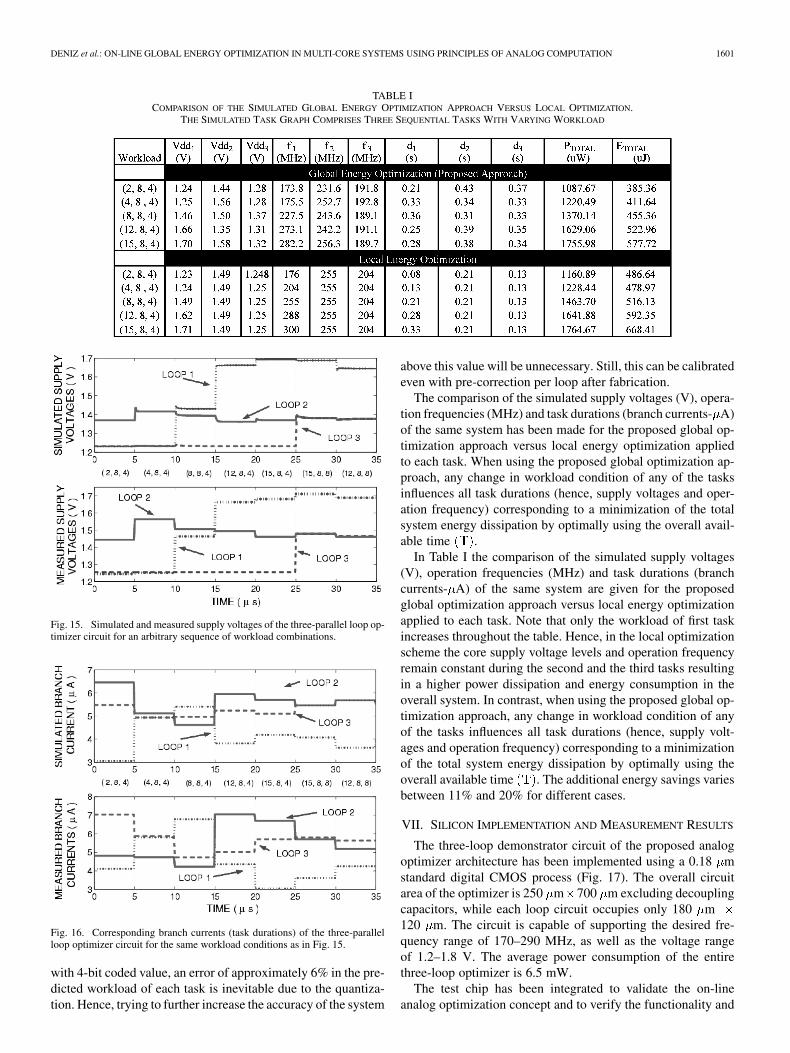
TABLE ICOMPARISON OF THE SIMULATED GLOBAL ENERGY OPTIMIZATION APPROACH VERSUS LOCAL OPTIMIZATION.
THE SIMULATED TASK GRAPH COMPRISES THREE SEQUENTIAL TASKS WITH VARYING WORKLOAD
Fig. 15. Simulated and measured supply voltages of the three-parallel loop op-timizer circuit for an arbitrary sequence of workload combinations.
Fig. 16. Corresponding branch currents (task durations) of the three-parallelloop optimizer circuit for the same workload conditions as in Fig. 15.
with 4-bit coded value, an error of approximately 6% in the pre-dicted workload of each task is inevitable due to the quantiza-tion. Hence, trying to further increase the accuracy of the system
above this value will be unnecessary. Still, this can be calibratedeven with pre-correction per loop after fabrication.
The comparison of the simulated supply voltages (V), opera-tion frequencies (MHz) and task durations (branch currents- A)of the same system has been made for the proposed global op-timization approach versus local energy optimization appliedto each task. When using the proposed global optimization ap-proach, any change in workload condition of any of the tasksinfluences all task durations (hence, supply voltages and oper-ation frequency) corresponding to a minimization of the totalsystem energy dissipation by optimally using the overall avail-able time .
In Table I the comparison of the simulated supply voltages(V), operation frequencies (MHz) and task durations (branchcurrents- A) of the same system are given for the proposedglobal optimization approach versus local energy optimizationapplied to each task. Note that only the workload of first taskincreases throughout the table. Hence, in the local optimizationscheme the core supply voltage levels and operation frequencyremain constant during the second and the third tasks resultingin a higher power dissipation and energy consumption in theoverall system. In contrast, when using the proposed global op-timization approach, any change in workload condition of anyof the tasks influences all task durations (hence, supply volt-ages and operation frequency) corresponding to a minimizationof the total system energy dissipation by optimally using theoverall available time . The additional energy savings variesbetween 11% and 20% for different cases.
VII. SILICON IMPLEMENTATION AND MEASUREMENT RESULTS
The three-loop demonstrator circuit of the proposed analogoptimizer architecture has been implemented using a 0.18 mstandard digital CMOS process (Fig. 17). The overall circuitarea of the optimizer is 250 m 700 m excluding decouplingcapacitors, while each loop circuit occupies only 180 m120 m. The circuit is capable of supporting the desired fre-quency range of 170–290 MHz, as well as the voltage rangeof 1.2–1.8 V. The average power consumption of the entirethree-loop optimizer is 6.5 mW.
The test chip has been integrated to validate the on-lineanalog optimization concept and to verify the functionality and

1602 IEEE JOURNAL OF SOLID-STATE CIRCUITS, VOL. 42, NO. 7, JULY 2007
Fig. 17. Chip microphotograph of the three-parallel loop optimizer.
performance of the circuit techniques used. The implementedcircuit also employs specific circuit blocks and dedicatedcontrol signals to ensure maximum configuration flexibilityand improve testability of the circuit. The test configurationcircuitry has crucial functionality on overall system insteadof its simple structure. The combinatorial circuit is respon-sible for the processing global power down, and several testconfiguration signals generated from the control signals withdedicated IO pads. The test configuration circuit, generatesglobal power-down signal, power-down signals for eachfeedback loop individually and power-down for stand-alonefrequency-to-current converter loop. The internal signals in crit-ical nodes can be accessed and observed off-chip, and feedbackloops can be configured to operate in open-loop configurationso that the loops can be closed through the external signalsfed to the blocks. This allows testing the circuit thoroughlyin a variety of configurations and conditions. Physical andgeometrical symmetry is one of the most important consider-ations in back-end design of sensitive analog circuits. Thus,common-centroid placement is preferred for translinear loops,current sources and differential pair layouts. 45 bending onthe signal paths have been implemented instead of 90 turns,since the parasitic resistance of the metal line with an angleof 90 is much larger that that of metal line with 45 bending.In the layout of analog optimizer, separate shielding has beenperformed to each sub-block. Noise generated by minority andmajority carriers have been treated separately, and a shieldhas been drawn for each, n-well and p-substrate depending onthe case. Although substrate and n-well biasing contacts areconnected to and nodes, they have not been shortedto shielding pick-up vias, which are also on the same metaland close to each other. Instead, they have been connected topower routings via different sets of vias, and are connected toeach other only at the highest metal layer. In this way, when anoise component is picked up by a shield, it does not coupledirectly to the substrate of the circuit, instead, it first couplesto the highest metal layer of the related power routing, and iscarried out of the chip via a few sheet resistances of that metal.
For the three-parallel loop configuration, 125 different work-load combinations are tested. A set of measured ghost circuitsupply voltages and pseudo-resistive network branch currents(task durations) are provided as well as the clock frequencyto be applied to the processing element in Fig. 18. Each data
Fig. 18. Measured outputs of the analog optimizer for six different workloadconditions. (a) The ghost circuit supply voltages. (b) The operating frequencies.(c) The corresponding branch currents.
set (three columns, represented with different filling patterns,showing three different measured data, i.e., supply voltages,clock frequencies and durations, respectively for the three tasksin Fig. 18) indicates the response of the circuit to a differentworkload condition for all three loops. The correspondingsupply voltage and the branch current values indicate thatthe proposed analog optimizer is capable of responding to

DENIZ et al.: ON-LINE GLOBAL ENERGY OPTIMIZATION IN MULTI-CORE SYSTEMS USING PRINCIPLES OF ANALOG COMPUTATION 1603
Fig. 19. Correlation between simulated and measured values of (a) the supplyvoltage and (b) the corresponding branch current (task duration) of the thirdloop.
varying operating conditions with a wide dynamic range. Theanalog optimizer block dictates the optimum operating voltageand duration of all three tasks for minimum system energyconsumption. It should be noted that measured supply voltagesrange from 1.2 V to 1.8 V, showing a significant (approximately35%) variation.
A comparison of measured and simulated branch currents aswell as loop supply voltages is provided in Fig. 19, for 10 dif-ferent workload conditions for the third network branch (mod-eling the third task of the TG). Each data point indicates themeasured response of the circuit versus to the simulated one at adifferent workload combination, showing a good agreement be-tween simulated and measured values. The branch current variesbetween 3 A and 8 A for different workloads during opera-tion, indicating that the duration of each task can be adjusted bymore than a factor of 2.
Fig. 20 shows the variation of the overall energy dissipationof the same system composed of three sequential tasks as afunction of changing workload conditions, calculated from mea-sured voltage/frequency and task duration values. To test theoptimality of this solution, the branch current values were per-turbed from their actual values (while keeping the sum constant)and the energy surface has been recalculated. The resulting en-ergy surface is clearly higher than the original solution for allworkload combinations and for all branch current perturbations,demonstrating that the original solution indeed is the minimumenergy surface.
Settling time of the ghost circuit supply voltages is important,due to the fact that circuit should be fast enough to track anychanges in the workload conditions for real time optimization.
Fig. 20. Comparision of the measured and the perturbed system energies.
Measured worst case settling time of the ghost circuit supplyvoltage for step-up response is less than 50 s. Similarly, mea-sured settling time for step-down response is 60 s.
VIII. CONCLUSION
In this work, the energy optimization problem in SoC/NoCapplications is discussed with a unique analog implementationapproach. The analogy that exists between the energy mini-mization problem under timing constraints in a general TG andthe power minimization problem under Kirchhoff’s current lawconstraints in an equivalent RN is exploited. The principlesof mapping an arbitrary task graph to an equivalent resistivenetwork are presented. A fully analog, current-based solution toimplement on-line energy minimization in complex multi-coresystems under varying workload conditions is demonstrated,which achieves significant overall energy savings comparedto the local energy minimization approach. The optimizedvoltage/frequency assignments are tailored to the instantaneousworkload information and fully adaptive to variations in processand temperature. The proposed architecture is oriented towardssupporting the challenges of energy management of multi-pro-cessing element architectures in SoC/NoC applications. Theoptimizer unit has a fast response time of 50 s, occupies asilicon area of 0.021 mm task and dissipates 2 mW/task.
The proposed analog optimizer solves the shortcomingsconcerning lack of ability to adapt the optimization results tochanging environmental conditions (e.g., temperature, processvariations) and on-line optimization (fast response time), as wellas low power consumption, which until today have limited theavailability of true on-chip (integrated) solutions for multipleprocessing elements. As such, the proposed optimizer can beused as a generic building block for on-line energy optimizationin complex systems.
APPENDIX A
As shown in Fig. 3, and must be executed in parallel ontwo different PEs, i.e., as a consequence of parallelism these twotasks must have the same duration . Similarly, in a re-sistive network branch consisting of two series connected resis-tors, each resistor must carry the same amount of branch current.

1604 IEEE JOURNAL OF SOLID-STATE CIRCUITS, VOL. 42, NO. 7, JULY 2007
Based on this analogy, all parallel tasks can be converted intoseries-connected branches in the equivalent resistive network.However, tasks mapped in series on a single PE, e.g., tasksand , can only be run sequentially in time. Consequently, theamount of available time will be split among the sequential tasksaccording to their actual workload. Hence, the amount of timenecessary for execution of task will be split among and
according to the actual workload of these twotasks. Similarly, in a RN branch of parallel connected resistorsthe main branch current will be shared proportionally betweenthe parallel branches according to KCL. Hence, all sequentialtasks can be represented by parallel-connected branches in theequivalent resistive network.
From the above explanations, the generalized steps involvedfor mapping the given task graph into a parallel-resistive net-work equivalent are as follows:
• Identify and assign the processing elements and the tasksmapped and scheduled on to the given system.
• Insert IN and OUT nodes into the given TG.• Simplify the task graph by replacing the edges representing
processing element sharing by equivalent edges capturingthe data/control dependencies between PEs.
• Convert all parallel tasks in the simplified TG to series-connected resistor branches in the resistive network.
• Convert all series tasks in the simplified TG to parallel-connected resistor branches in the resistive network.
• Replace the IN node by a DC current source modeling theTG period and the OUT node by the ground connectionproviding the necessary current path in the resistive net-work.
However, not every task graph is in series/parallel configu-ration. The TG given in Fig. 21(a) is an example of such nonseries/parallel configuration. Still, an equivalent RN can bemapped from the given TG without violating the correspondingtiming constraints as shown in Fig. 21(b), where the cut-setsare highlighted by dashed lines. Recall that can only startafter processing of on the first processing element and and
on the second processing element are finished. Similarly,in order to finish the assigned job just in time, execution timeof tasks and should be equal to the summation of taskdurations and , and and respectively.
Here, timing constraints, e.g., ,and , are intrinsically satisfied due to KCL con-straints in the RN, i.e., , , and
respectively. Hence, the equivalent RN of controlledresistors can be mapped for any arbitrary TG, where each devicecurrent represents the available time for the corresponding task,
theoverall available timetocomplete the jobwithin thedefineddeadline and the device conductances the corresponding task.
Although the applied mapping scheme has a certain resem-blance to creating the dual of a given task graph, it is important toemphasize that the mapping of a given task graph to its equivalentresistive network is based on converting the time domain relationbetween tasks into equivalent resistive network currents.
APPENDIX B
As already mentioned, the concept of system stability needsto be considered when several components adopt dynamic poli-
Fig. 21. (a) An example task graph of non-series/parallel configuration. (b) Theequivalent resistive-network of this task graph.
cies to control energy consumption and performance. Possibleoscillations in energy/performance space that could be causedby applied power management policies are undesirable, andshould be avoided. In this section it will be shown that thedynamic behavior of each device control loop is governed bya single-dominant-pole transfer function, and that the entiresystem (the centralized optimizer unit) always converges to astable operating point for a given set of workload values.
In order to derive the transfer function of the feedback controlloop, the loop is opened on the resistive network. Hence, thebranch current is treated as the input current (variable) andthe pseudo-resistor controlling current is treated as the outputcurrent. Note that , , , , are constant biasing currentsused in the feedback loop.
From the loop dynamics, the output current can be writtenas in (B1). Note that one can show the small variations in thevalue of a variable as , where lower case represents thevariations in the value of the variable. Using this definition, theoutput current can be written as given in (B2).
(B1)
(B2)

DENIZ et al.: ON-LINE GLOBAL ENERGY OPTIMIZATION IN MULTI-CORE SYSTEMS USING PRINCIPLES OF ANALOG COMPUTATION 1605
Note that we can express the ratios of the current representa-tions of the ghost circuit supply voltage and the operating fre-quency as well as the current consumption of the ghost circuitand their variations in terms of the ratio of the input current andits variation as given in (B3) [25].
and and
(B3)
Finally, the device conductance controlling current being theoutput current and the related device current being the inputcurrent the small signal behavior of the feedback loop can bewritten as given in (B4), since branch conductances are linearlyproportional to their controlling current . Hence, it is shownthat the dynamic behavior of each branch control loop (feedbackloop) is governed by a single-dominant-pole transfer function.
(B4)
(B5)
(B6)
Now, consider a resistive network consisting of three parallelbranches to illustrate the stability properties of the system. If wewrite the first branch current in the resistive network comprisingthree parallel branches in terms of the resistive network biasingcurrent and the other branch currents, we get (B5), whereand represents the device conductance and the variations inthe conductance value respectively. Now that if we replace each
quantity in (B5) by , and substituting (B4)where ever suitable, we can finally write (B6).
Consequently (B6) will look like (B7) after doing the neces-sary mathematical operations in order to determine the charac-teristic equation of the system.
(B7)
Now, if we rewrite the characteristic equation of the systemas given in (B8), we can check the stability of the system byapplying the Routh criterion.
(B8)
TABLE IIROUTH TABLE OF THE CHARACTERISTICS EQUATION OF THE SYSTEM
The principal stability criterion for linear systems states thata system is stable if all poles of its transfer function lie in theleft-half of the complex s-plane. Equivalently, a system is stableif the real parts of all roots of its characteristic equation arenegative. Note that a root of the characteristic equation is syn-onymous with a system pole. To apply Routh’s criterion, theRouth’s Table should be created as given in Table II. The Routhcriterion is applied by examining the sign of the coefficient inthe column headed by . The number of sign changes in the el-ements of this column, taken in order, is equal to the number ofroots of the characteristic equation that have positive real parts.Hence, in order to show that the system is stable we shouldverify that the sign of the expression is positive,since all the other components of the first column of the routhtable are positive quantities. Note that all and quantities arepositive real values. Thus, , and are intrinsically positivefor all or values. Note that is also always positive for all
or values, since definition of guarantiesthat the multiplicative factor in is always positive.After doing all the necessary multiplications, it is proved thatthe sign of the mathematical operation is alwayspositive, guaranteeing that the proposed system is stable.
REFERENCES
[1] L. Benini, A. Bogliolo, and G. DeMicheli, “A survey of design tech-niques for system-level dynamic power management,” IEEE Trans. VeryLarge Scale Integrat. (VLSI) Syst., vol. 8, no. 3, pp. 299–316, Mar. 2000.
[2] T. Simunic, L. Benini, P. Glynn, and G. DeMicheli, “Event-drivenpower management,” IEEE Trans. Comput.-Aided Design Integrat.Circuits Syst., vol. 20, no. 7, pp. 840–857, Jul. 2001.
[3] K. Flautner, D. Flynn, and M. Rives, “A combined hardware-softwareapproach for low-power SoCs: Applying adaptive voltage scaling andintelligent energy management software,” in Proc. System-on-Chip andASIC Design Conf. (DesignCon), Jan. 2003.
[4] S. M. Martin, K. Flautner, T. Mudge, and D. Blaauw, “Combined dy-namic voltage scaling and adaptive body biasing for lower power mi-croprocessors under dynamic workloads,” in Proc. Int. Conf. ComputerAided Design, San Jose, CA, Nov. 2002, pp. 721–725.
[5] D. M. Monticelli, “Taking a system approach to energy management,”in Proc. 29th European Solid-State Circuits Conf. (ESSCIRC), Estoril,Portugal, Sep. 2003, vol. 1, pp. 15–19.
[6] T. Elmas, “Modeling workload breakdown properties of the MPEG-2decoder application with hidden Markow processes,” Koc Univ., Is-tanbul, Turkey, Tech. Rep., 2004.
[7] S. Yaldiz, A. Demir, S. Tasiran, P. Ienne, and Y. Leblebici, “Char-acterizing and exploiting task-load variability and correlation for en-ergy management,” in IEEE 3rd Workshop on Embedded Systems forReal-Time Multimedia, New York, Sep. 2005.
[8] S. M. Ross, Introduction to Probability Models, 6th ed. New York:Academic Press, 1997.
[9] M. L. Puterman, Finite Markov Decision Processes. New York:Wiley, 1994.
[10] N. Pazos, A. Maxiaguine, P. Ienne, and Y. Leblebici, “Parallel mod-eling paradigm in multimedia applications: Mapping and schedulingonto a multiprocessor system-on-chip platform,” in Proc. Int. GlobalSignal Processing Conf., Santa Clara, CA, Sep. 2004.
[11] L. Yan, J. Luo, and N. K. Jha, “Combined dynamic voltage scalingand adaptive body biasing for heterogeneous distributed real-time em-bedded systems,” in Proc. Int. Conf. Computer Aided Design, Wash-ington, DC, Jun. 2003, pp. 30–37.

1606 IEEE JOURNAL OF SOLID-STATE CIRCUITS, VOL. 42, NO. 7, JULY 2007
[12] R. Jejurikar and R. Gupta, “Dynamic voltage scaling for systemwideenergy minimization in real-time embedded systems,” in Proc. Int.Symp. Low Power Electronics and Design, Newport Beach, CA, 2004,pp. 78–81.
[13] Y. Zhang, X. S. Hu, and D. Z. Chen, “Energy minimization of real-timetasks on variable voltage processors with transition energy overhead,”in Proc. ASPDAC, 2003, pp. 65–70.
[14] A. Andrei, M. Schmitz, P. Eles, Z. Peng, and B. M. Al-Hashimi,“Overhead-conscious voltage selection for dynamic and leakageenergy reduction of time-constrained systems,” in Proc. DATE, 2004,pp. 105–118.
[15] Y. Zhang, X. Hu, and D. Chen, “Task scheduling and voltage selectionfor energy minimization,” in Proc. DAC, 2002, pp. 183–188.
[16] Z. Toprak, Y. Leblebici, and E. Vittoz, “On-line global energy opti-mization in multi-core embedded systems based on analog computa-tion,” in Proc. 32nd ESSCIRC, Montreux, Switzerland, 2006.
[17] J. C. Maxwell, A Treatise on Electricity and Magnetism, 3rd ed. Ox-ford, U.K.: Clarendon, 1892, vol. 1, pp. 399–410.
[18] The Instrumentation, Systems and Automation Society (ISA) HomePage. [Online]. Available: http://www.isa.org
[19] E. A. Vittoz, “Analog VLSI for collective computation,” in Proc. IEEEInt. Conf. Electronics, Circuits and Systems, 1998, pp. 3–6.
[20] B. Gilbert, “Translinear circuits: A proposed classification,” Electron.Lett., vol. 11, no. 1, pp. (14–16, 1975.
[21] E. Vittoz, “A basic property of MOS transistors and its circuit implica-tions,” in Workshop on Compact Modeling (WCM-MSM 2003), Singa-pore, Feb. 2003.
[22] E. A. Vittoz, “Pseudo-resistive networks and their applications toanalog collective computation,” in Proc. 7th Int. Conf. ArtificialNeural Networks, Lausanne, Switzerland, Oct. 1997, pp. 1133–1150.
[23] E. A. Vittoz, “Analog VLSI signal processing: Why, where, and how?,”J. VLSI Signal Process. Syst., vol. 8, no. 1, pp. 27–44, 1994.
[24] E. Vittoz and X. Arreguit, “Linear networks based on transistors,” Elec-tron. Lett., vol. 29, pp. 297–299, 1993.
[25] Z. T. Deniz, “Multi-unit global energy management and optimizationfor network-on-chip applications,” Ph.D. dissertation, EPFL, Lau-sanne, Switzerland, 2006.
Zeynep Toprak Deniz (M’06) received the B.S.degree in electronics and telecommunication engi-neering from Istanbul Technical University in 1999.From November 1999 to July 2002, she worked as anAnalog Design Engineer at Alcatel MicroelecronicsR&D group in Turkey, where she contributed todesign, layout and verification of several buildingblocks for various projects including DCDC con-verters, PLLs, and VCXO. In September 2000,she joined Sabanci University (SU) as a graduatestudent. She received the M.Sc. degree in electronics
engineering in September 2001 from SU. She received the Ph.D. degree inelectrical engineering from Ecole Polytechnique Federale de Lausanne (EPFL),Switzerland, in 2006.
In July 2002, she joined ST Microelectronics in Turkey as an Analog De-sign Engineer, where she worked in design and layout of the high-performance,PLL-based low-jitter clock and data recovery (CDR) circuits using aided ac-quisition in standardCMOS technology. In January 2003, she joined CSEM(Centre Suisse Electronique et Microtechnique), where she was involved in thedesign of three different regulators for PA, VCO and digital, two step-up cir-cuits and RC oscillator sub-blocks for a wireless communication node operatedon two switching AA batteries. Since March 2007, she has been a Research StaffMember at IBM T. J. Watson Research Center.
Yusuf Leblebici (M’90–SM’98) received the B.S.and M.S. degrees in electrical engineering fromIstanbul Technical University in 1984 and 1986,respectively, and the Ph.D. degree in electrical andcomputer engineering from the University of Illinoisat Urbana-Champaign (UIUC) in 1990.
Between 1991 and 2001, he worked as a facultymember at UIUC, at Istanbul Technical University,and at Worcester Polytechnic Institute (WPI), wherehe established and directed the VLSI Design Labora-tory, and also served as a Project Director at the New
England Center for Analog and Mixed-Signal IC Design. He also worked asthe Microelectronics Program Coordinator at Sabanci University. Since January2002, he has been a full Professor at the Swiss Federal Institute of Technology inLausanne (EPFL), and Director of the Microelectronic Systems Laboratory. Hisresearch interests include design of high-speed CMOS digital and mixed-signalintegrated circuits, computer-aided design of VLSI systems, modeling and sim-ulation of nano-electronic circuits, intelligent sensor interfaces, and VLSI re-liability analysis. He is the coauthor of two textbooks, Hot-Carrier Reliabilityof MOS VLSI Circuits (Kluwer Academic, 1993) and CMOS Digital IntegratedCircuits: Analysis and Design (McGraw Hill, 1996, 1999, and 2003), as well asnumerous scientific articles published in international journals and conferences.
Dr. Leblebici has served on the organizing and steering committees of the1995 European Conference on Circuit Theory and Design (ECCTD 1995), the2004 European Workshop on Microelectronics Education (EWME 2004), andas Co-Chairman of the Joint European Solid-State Circuits Conference/Euro-pean Solid-State Device Research Conference (ESSCIRC-ESSDERC 2006). Healso served as an Associate Editor of IEEE TRANSACTIONS ON CIRCUITS AND
SYSTEMS II, and as an Associate Editor of IEEE TRANSACTIONS ON VLSI. Hereceived the Young Scientist Award of the Turkish Scientific and TechnologicalResearch Councils in 1995, and the Joseph Samuel Satin Distinguished FellowAward of the Worcester Polytechnic Institute in 1999.
Eric A. Vittoz (M’72–SM’87–F’89–LF’04) re-ceived the M.S. and Ph.D. degrees in electricalengineering from the Swiss Federal Institute ofTechnology in Lausanne (EPFL) in 1961 and 1969,respectively.
He joined the Watchmakers Electronic Center(CEH) in 1962 as a member of the team that de-veloped the first quartz watch. He became head ofthe Advanced Circuit Department at CEH in 1967and was appointed Vice Director and head of theApplications Division in 1971. In 1984, he took the
responsibility of the Circuits and Systems Research Division of the newlyfounded CSEM (Swiss Center for Electronics and Microtechnology), where hewas appointed Executive Vice-President in 1991, head of Integrated Circuitsand Systems, then head of Advanced Microelectronics after 1997. Since 2004,he is retired from CSEM after spending three years of partial retirement asa Fellow researcher. Since 1975, he has taught analog circuit design, andsupervising undergraduate and graduate student projects at EPFL, where hebecame Professor in 1982. He has authored or co-authored more than 150papers and holds 26 patents in the fields of very low-power microelectronics,compact transistor modeling, analog CMOS circuit design and biology-inspiredanalog VLSI.
Dr. Vittoz has been involved in the formation of the IEEE Solid-State CircuitsSociety and was a member of its AdCom from 1996 to 1999. He was a memberof the European Program Committee of ISSCC from 1977 to 1989, and duringmore than 25 years, a member of the Steering Committee of ESSCIRC, theEuropean Solid-State Circuits Conference. He is a Life Fellow of the IEEE, andhe was the recipient of the 2004 IEEE Solid-State Circuits Award.