Fault Current Interruption by the Dynamic Voltage Restorer
8
IEEE TRANSACTIONS ON POWER DELIVERY, VOL. 28, NO. 2, APRIL 2013 903 Fault Current Interruption by the Dynamic Voltage Restorer Firouz Badrkhani Ajaei, Student Member, IEEE, Shahrokh Farhangi, and Reza Iravani, Fellow, IEEE Abstract—This paper introduces and evaluates an auxiliary con- trol strategy for downstream fault current interruption in a radial distribution line by means of a dynamic voltage restorer (DVR). The proposed controller supplements the voltage-sag compensa- tion control of the DVR. It does not require phase-locked loop and independently controls the magnitude and phase angle of the in- jected voltage for each phase. Fast least error squares digital fil- ters are used to estimate the magnitude and phase of the measured voltages and effectively reduce the impacts of noise, harmonics, and disturbances on the estimated phasor parameters, and this en- ables effective fault current interrupting even under arcing fault conditions. The results of the simulation studies performed in the PSCAD/EMTDC software environment indicate that the proposed control scheme: 1) can limit the fault current to less than the nom- inal load current and restore the point of common coupling voltage within 10 ms; 2) can interrupt the fault current in less than two cy- cles; 3) limits the dc-link voltage rise and, thus, has no restrictions on the duration of fault current interruption; 4) performs satisfac- torily even under arcing fault conditions; and 5) can interrupt the fault current under low dc-link voltage conditions. Index Terms—Digital filters, dynamic voltage restorer (DVR), fault current interrupting, multiloop control. I. INTRODUCTION T HE DYNAMIC voltage restorer (DVR) is a custom power device utilized to counteract voltage sags [1], [2]. It in- jects controlled three-phase ac voltages in series with the supply voltage, subsequent to a voltage sag, to enhance voltage quality by adjusting the voltage magnitude, waveshape, and phase angle [3]–[6]. Fig. 1 shows the main components of a DVR (i.e., a se- ries transformer , a voltage- source converter (VSC), a har- monic filter, a dc-side capacitor , and an energy storage de- vice [7], [8]). The line-side harmonic filter [5] consists of the leakage inductance of the series transformer and the filter capacitor . The DVR is conventionally bypassed during a downstream fault to prevent potential adverse impacts on the fault and to protect the DVR components against the fault current [9]–[11]. A technically elaborate approach to more efficient utilization of the DVR is to equip it with additional controls and enable it Manuscript received April 27, 2012; revised August 04, 2012 and September 17, 2012; accepted September 22, 2012. Date of publication February 25, 2013; date of current version March 21, 2013. Paper no. TPWRD-00434-2012. F. Badrkhani Ajaei and R. Iravani are with the Department of Electrical and Computer Engineering, University of Toronto, Toronto, ON M5S 3G4, Canada (e-mail: [email protected]; [email protected]). S. Farhangi is with the School of Electrical and Computer Engineering, Uni- versity of Tehran, Tehran 14395-515, Iran (e-mail: [email protected]). Digital Object Identifier 10.1109/TPWRD.2012.2220864 Fig. 1. Schematic diagram of a DVR with a line-side harmonic filter. also to limit or interrupt the downstream fault currents. A con- trol approach to enable a DVR to serve as a fault current lim- iter is provided in [9]. The main drawback of this approach is that the dc-link voltage of the DVR increases due to real power absorption during fault current-limiting operation and necessi- tates a switch to bypass the DVR when the protective relays, depending on the fault conditions, do not rapidly clear the fault. The dc-link voltage increase can be mitigated at the cost of a slow-decaying dc fault current component using the methods introduced in [7] and [12]. To overcome the aforementioned limitations, this paper pro- poses an augmented control strategy for the DVR that provides: 1) voltage-sag compensation under balanced and unbalanced conditions and 2) a fault current interruption (FCI) function. The former function has been presented in [13] and the latter is de- scribed in this paper. It should be noted that limiting the fault current by the DVR disables the main and the backup protection (e.g., the distance and the overcurrent relays). This can result in prolonging the fault duration. Thus, the DVR is preferred to reduce the fault current to zero and interrupt it and send a trip signal to the up- stream relay or the circuit breaker (CB). It should be noted that the FCI function requires 100% voltage injection capability. Thus, the power ratings of the series transformer and the VSC would be about three times those of a conventional DVR with about 30%–40% voltage injection capability. This leads to a more expensive DVR system. Economic feasibility of such a DVR system depends on the importance of the sensitive load protected by the DVR and the cost of the DVR itself. The performance of the proposed control scheme is evalu- ated through various simulation studies in the PSCAD/EMTDC platform. The study results indicate that the proposed control strategy: 1) limits the fault current to less than the nominal load current and restores the PCC voltage within less than 10 ms, and interrupts the fault current within two cycles; 2) it can be used in four- and three-wired distribution systems, and single-phase 0885-8977/$31.00 © 2013 IEEE
Transcript of Fault Current Interruption by the Dynamic Voltage Restorer

IEEE TRANSACTIONS ON POWER DELIVERY, VOL. 28, NO. 2, APRIL 2013 903
Fault Current Interruption bythe Dynamic Voltage Restorer
Firouz Badrkhani Ajaei, Student Member, IEEE, Shahrokh Farhangi, and Reza Iravani, Fellow, IEEE
Abstract—This paper introduces and evaluates an auxiliary con-trol strategy for downstream fault current interruption in a radialdistribution line by means of a dynamic voltage restorer (DVR).The proposed controller supplements the voltage-sag compensa-tion control of the DVR. It does not require phase-locked loop andindependently controls the magnitude and phase angle of the in-jected voltage for each phase. Fast least error squares digital fil-ters are used to estimate the magnitude and phase of the measuredvoltages and effectively reduce the impacts of noise, harmonics,and disturbances on the estimated phasor parameters, and this en-ables effective fault current interrupting even under arcing faultconditions. The results of the simulation studies performed in thePSCAD/EMTDC software environment indicate that the proposedcontrol scheme: 1) can limit the fault current to less than the nom-inal load current and restore the point of common coupling voltagewithin 10 ms; 2) can interrupt the fault current in less than two cy-cles; 3) limits the dc-link voltage rise and, thus, has no restrictionson the duration of fault current interruption; 4) performs satisfac-torily even under arcing fault conditions; and 5) can interrupt thefault current under low dc-link voltage conditions.
Index Terms—Digital filters, dynamic voltage restorer (DVR),fault current interrupting, multiloop control.
I. INTRODUCTION
T HEDYNAMIC voltage restorer (DVR) is a custom powerdevice utilized to counteract voltage sags [1], [2]. It in-
jects controlled three-phase ac voltages in series with the supplyvoltage, subsequent to a voltage sag, to enhance voltage qualityby adjusting the voltagemagnitude, waveshape, and phase angle[3]–[6]. Fig. 1 shows the main components of a DVR (i.e., a se-ries transformer , a voltage- source converter (VSC), a har-monic filter, a dc-side capacitor , and an energy storage de-vice [7], [8]). The line-side harmonic filter [5] consists of theleakage inductance of the series transformer and the filtercapacitor .The DVR is conventionally bypassed during a downstream
fault to prevent potential adverse impacts on the fault and toprotect the DVR components against the fault current [9]–[11].A technically elaborate approach to more efficient utilization ofthe DVR is to equip it with additional controls and enable it
Manuscript received April 27, 2012; revised August 04, 2012 and September17, 2012; accepted September 22, 2012. Date of publication February 25, 2013;date of current version March 21, 2013. Paper no. TPWRD-00434-2012.F. Badrkhani Ajaei and R. Iravani are with the Department of Electrical and
Computer Engineering, University of Toronto, Toronto, ON M5S 3G4, Canada(e-mail: [email protected]; [email protected]).S. Farhangi is with the School of Electrical and Computer Engineering, Uni-
versity of Tehran, Tehran 14395-515, Iran (e-mail: [email protected]).Digital Object Identifier 10.1109/TPWRD.2012.2220864
Fig. 1. Schematic diagram of a DVR with a line-side harmonic filter.
also to limit or interrupt the downstream fault currents. A con-trol approach to enable a DVR to serve as a fault current lim-iter is provided in [9]. The main drawback of this approach isthat the dc-link voltage of the DVR increases due to real powerabsorption during fault current-limiting operation and necessi-tates a switch to bypass the DVR when the protective relays,depending on the fault conditions, do not rapidly clear the fault.The dc-link voltage increase can be mitigated at the cost of aslow-decaying dc fault current component using the methodsintroduced in [7] and [12].To overcome the aforementioned limitations, this paper pro-
poses an augmented control strategy for the DVR that provides:1) voltage-sag compensation under balanced and unbalancedconditions and 2) a fault current interruption (FCI) function. Theformer function has been presented in [13] and the latter is de-scribed in this paper.It should be noted that limiting the fault current by the DVR
disables the main and the backup protection (e.g., the distanceand the overcurrent relays). This can result in prolonging thefault duration. Thus, the DVR is preferred to reduce the faultcurrent to zero and interrupt it and send a trip signal to the up-stream relay or the circuit breaker (CB).It should be noted that the FCI function requires 100%
voltage injection capability. Thus, the power ratings of theseries transformer and the VSC would be about three timesthose of a conventional DVR with about 30%–40% voltageinjection capability. This leads to a more expensive DVRsystem. Economic feasibility of such a DVR system dependson the importance of the sensitive load protected by the DVRand the cost of the DVR itself.The performance of the proposed control scheme is evalu-
ated through various simulation studies in the PSCAD/EMTDCplatform. The study results indicate that the proposed controlstrategy: 1) limits the fault current to less than the nominal loadcurrent and restores the PCC voltage within less than 10 ms, andinterrupts the fault current within two cycles; 2) it can be usedin four- and three-wired distribution systems, and single-phase
0885-8977/$31.00 © 2013 IEEE

904 IEEE TRANSACTIONS ON POWER DELIVERY, VOL. 28, NO. 2, APRIL 2013
Fig. 2. Per-phase block diagram of the DVR control system in FCI mode.
configurations; 3) does not require phase-locked loops; 4) is notsensitive to noise, harmonics, and disturbances and provides ef-fective fault current interruption even under arcing fault condi-tions; and 5) can interrupt the downstream fault current underlow dc-link voltage conditions.
II. PROPOSED FCI CONTROL STRATEGY
The adopted DVR converter is comprised of three indepen-dent H-bridge VSCs that are connected to a common dc-linkcapacitor. These VSCs are series connected to the supply grid,each through a single-phase transformer. The proposed FCIcontrol system consists of three independent and identicalcontrollers one for each single-phase VSC of the DVR.Assume the fundamental frequency components of the supply
voltage , load voltage , and the injected voltage , Fig. 1are
(1)
(2)
(3)
Two identical least error squares (LES) filters [14] are usedto estimate the magnitudes and phase angles of the pha-
sors corresponding to and (i.e., and
, respectively in 5 ms [13]).The FCI function requires a phasor parameter estimator (dig-
ital filter) which attenuates the harmonic contents of the mea-sured signal. To attenuate all harmonics, the filter must have afull-cycle data window length which leads to one cycle delay inthe DVR response. Thus, a compromise between the voltage in-jection speed and disturbance attenuation is made. The designedLES filters utilize a data window length of 50 samples at thesampling rate of 10 kHz and, hence, estimate the voltage phasorparameters in 5 ms. Fig. 3 depicts the frequency response of theLES filters and indicates significant attenuation of voltage noise,harmonics, and distortions at frequencies higher than 200 Hzand lower than 50 Hz. Reference [13] demonstrates the effec-tiveness of this filter in attenuating the noise, harmonics, anddistortions for the sag compensation mode of operation as well.The next section shows that this filter also performs satisfacto-rily in the FCI operation mode, even under arcing fault condi-tions where the measured voltage and current signals are highlydistorted.Fig. 2 shows a per-phase block diagram of the proposed DVR
control system corresponding to the FCI operation mode, whereis the nominal rms phase voltage. The control system of
Fig. 3. Magnitude of the LES filters frequency response.
Fig. 2 utilizes , , the dc-link voltage , and the harmonicfilter capacitor current as the input signals. The reportedstudies in this paper are based on the overcurrent fault detectionmethod of [7] and [12]. The fault detection mechanism for eachphase is activated when the absolute value of the instantaneouscurrent exceeds twice the rated load current.The proposedmultiloop control system [3], [8], [9], [15]–[20]
includes an outer control loop (voltage phasor control) and aninner control loop (instantaneous voltage control). The innerloop provides damping for the transients caused by the DVRharmonic filter [18] and [21], and improves the dynamic re-sponse and stability of the DVR. The inner loop is shared by thesag compensation and the FCI functions. When a downstreamfault is detected, the outer loop controls the injected voltagemagnitude and phase angle of the faulty phase(s) and reducesthe load-side voltage to zero, to interrupt the fault current andrestore the PCC voltage. The DVR “outer” voltage phasor con-trol and “inner” instantaneous voltage control, corresponding toeach phase, are described in the following two subsections.
A. Voltage Phasor Control System
In the FCI operation mode, the required injected voltagephasor is equal to the source voltage phasor, but in phase op-
position [i.e., the injected phasor is controlledto be ]. Performance of the voltage phasor control,in terms of transient response, speed, and steady-state error,is enhanced by independent control of voltage magnitude andphase, and incorporating feedforward signals to the feedbackcontrol system [17], [18], [21]–[27]. Fig. 2 shows two propor-tional-integral (PI) controllers ( and ) that are used toeliminate the steady-state errors of the magnitude and phase ofthe injected voltage, respectively. Parameters of each controller

BADRKHANI AJAEI et al.: FAULT CURRENT INTERRUPTION BY THE DVR 905
are determined to achieve a fast response with zero steady-stateerror.The output of the phasor control system is a reference phasor
denoted by . To eliminate the effects of thedc-link voltage variations on the injected voltages, is nor-
malized by . The magnitude and the phase angle of areindependently calculated and the magnitude is passed through alimiter (Fig. 2). The resulting phasor magnitude and phase angleare converted to the sinusoidal signal , which is the referencesignal for the instantaneous voltage control.
B. Instantaneous Voltage-Control System
Under ideal conditions, a voltage sag can be effectively com-pensated if the output of the phasor-based controller is di-rectly fed to the sinusoidal pulse-width modulation (SPWM)unit. However, resonances of the harmonic filter cannot be elim-inated under such conditions. Therefore, to improve the stabilityand dynamic response of the DVR, an instantaneous injectedvoltage controller and a harmonic filter capacitor current con-troller are used to attenuate resonances.The generated reference signal for the injected voltage
is compared with the measured injected voltage , and theerror is fed to the voltage controller. As shown in Fig. 2, theoutput of the voltage controller is the reference signal forthe filter capacitor current control loop. It is compared with themeasured capacitor current , and the error is fed to the cur-rent controller.The steady-state error of the proposed control system is fully
eliminated by the PI controllers in the outer control loop (i.e.,and ), which track dc signals (magnitude and phase angle).Therefore, there is no need for higher order controllers in theinner control loop which are designed based on sinusoidal ref-erences. Thus, in Fig. 2, and are pure gains and ,respectively.A large results in amplification of the DVR filter reso-
nance and can adversely impact the system stability [18]. Thus,the transient response of the DVR is enhanced by a feedforwardloop, and a small proportional gain is utilized as the voltage con-troller. A large damps the harmonic filter resonance moreeffectively, but it is limited by practical considerations (e.g.,amplification of capacitor current noise, measurement noise,and dc offset [18]). Therefore, the lowest value of the propor-tional gain which can effectively damp the resonances is uti-lized. The output of the current controller is added to the feed-forward voltage to derive the signal for the PWM generator.
III. STUDY RESULTS
Fig. 4 depicts a single-line diagram of a power systemwhich is used to evaluate the performance of the proposedDVR control system under different fault scenarios, in thePSCAD/EMTDC software environment. A 525-kVA DVRsystem is installed on the 0.4-kV feeder, to protect a 500-kVA,0.90 lagging power factor load against voltage sags. Param-eters of the simulated power system and the DVR are givenin Appendix A. In the reported studies, the base voltage forper-unit values is the nominal phase voltage. Besides, voltage
Fig. 4. Single-line diagram of the system used for simulation studies.
Fig. 5. (a) Voltages at . (b) Fault currents, during downstream three-phasefault when the DVR is inactive (bypassed).
and current waveforms of phases A, B, and C are plotted bysolid, dashes, and dotted lines, respectively.
A. Three-Phase Downstream Fault
The system is subjected to a three-phase short circuit with anegligible fault resistance at 20 ms at . Prior to thefault inception, the DVR is inactive (in standby mode) (i.e., theprimary windings of the series transformers are shorted by theDVR). During the fault if the DVR is bypassed, the voltageat Bus3 drops to 0.77 p.u. and the fault current increases toabout 17 times the rated load current (Fig. 5). Fig. 6 shows FCIperformance of the proposed DVR control system during thefault. Fig. 6(a)–(c), respectively, shows the three-phase injectedvoltages, the restored three-phase supply-side voltages, and thethree-phase load-side voltages which are reduced to zero to in-terrupt the fault currents. The slightly injected voltage by theDVR before the fault initiation [Fig. 6(a)] is the voltage dropacross the series impedance of the DVR series transformer sec-ondary winding.Fig. 6(d) shows the line currents (i.e., the currents passing
through the DVR). Fig. 6(d) illustrates that the proposed FCImethod limits the maximum fault current to about 2.5 times thenominal value of the load current and interrupts the fault cur-rents in less than 2 cycles. Fig. 6(e) depicts variations of thedc-link voltage during the FCI operation, and indicates that thedc-link voltage rise under the worst case (i.e., a severe three-phase fault) is about 15% and occurs during the first 5 ms afterfault inception.
906 IEEE TRANSACTIONS ON POWER DELIVERY, VOL. 28, NO. 2, APRIL 2013
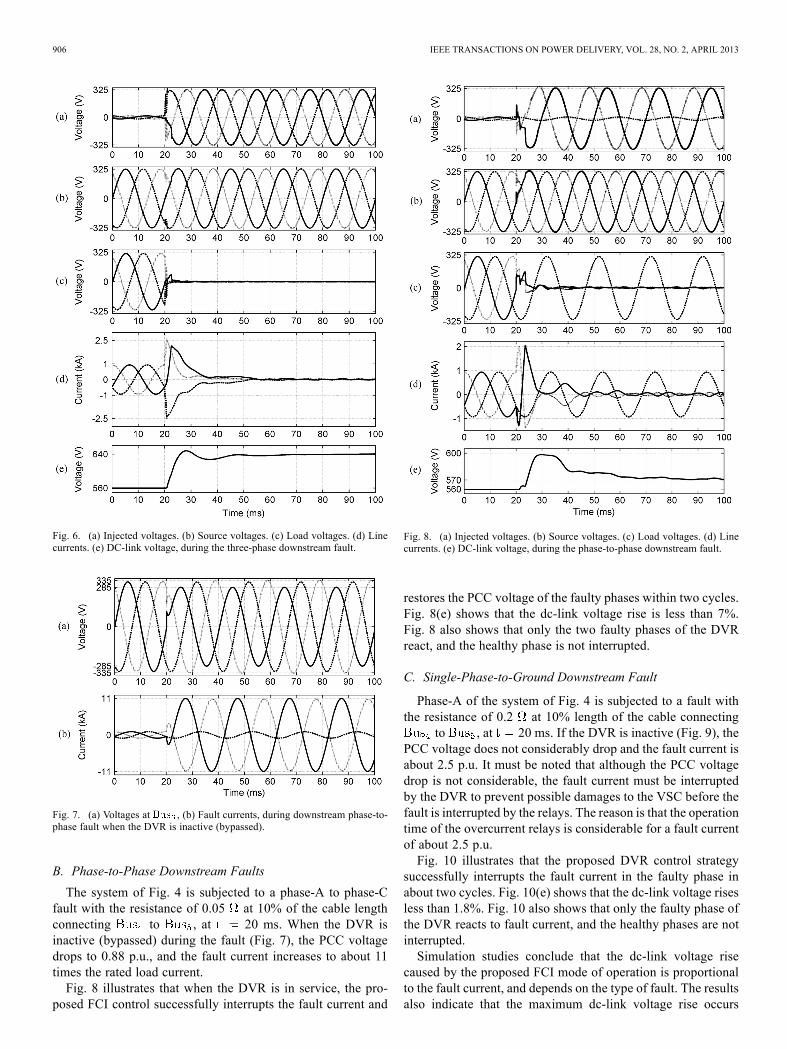
Fig. 6. (a) Injected voltages. (b) Source voltages. (c) Load voltages. (d) Linecurrents. (e) DC-link voltage, during the three-phase downstream fault.
Fig. 7. (a) Voltages at , (b) Fault currents, during downstream phase-to-phase fault when the DVR is inactive (bypassed).
B. Phase-to-Phase Downstream Faults
The system of Fig. 4 is subjected to a phase-A to phase-Cfault with the resistance of 0.05 at 10% of the cable lengthconnecting to , at 20 ms. When the DVR isinactive (bypassed) during the fault (Fig. 7), the PCC voltagedrops to 0.88 p.u., and the fault current increases to about 11times the rated load current.Fig. 8 illustrates that when the DVR is in service, the pro-
posed FCI control successfully interrupts the fault current and
Fig. 8. (a) Injected voltages. (b) Source voltages. (c) Load voltages. (d) Linecurrents. (e) DC-link voltage, during the phase-to-phase downstream fault.
restores the PCC voltage of the faulty phases within two cycles.Fig. 8(e) shows that the dc-link voltage rise is less than 7%.Fig. 8 also shows that only the two faulty phases of the DVRreact, and the healthy phase is not interrupted.
C. Single-Phase-to-Ground Downstream Fault
Phase-A of the system of Fig. 4 is subjected to a fault withthe resistance of 0.2 at 10% length of the cable connecting
to , at 20 ms. If the DVR is inactive (Fig. 9), thePCC voltage does not considerably drop and the fault current isabout 2.5 p.u. It must be noted that although the PCC voltagedrop is not considerable, the fault current must be interruptedby the DVR to prevent possible damages to the VSC before thefault is interrupted by the relays. The reason is that the operationtime of the overcurrent relays is considerable for a fault currentof about 2.5 p.u.Fig. 10 illustrates that the proposed DVR control strategy
successfully interrupts the fault current in the faulty phase inabout two cycles. Fig. 10(e) shows that the dc-link voltage risesless than 1.8%. Fig. 10 also shows that only the faulty phase ofthe DVR reacts to fault current, and the healthy phases are notinterrupted.Simulation studies conclude that the dc-link voltage rise
caused by the proposed FCI mode of operation is proportionalto the fault current, and depends on the type of fault. The resultsalso indicate that the maximum dc-link voltage rise occurs

BADRKHANI AJAEI et al.: FAULT CURRENT INTERRUPTION BY THE DVR 907
Fig. 9. (a) Voltages at . (b) Fault currents, during the downstream single-phase-to-ground fault when the DVR is inactive (bypassed).
Fig. 10. (a) Injected voltages. (b) Source voltages. (c) Load voltages. (d) Linecurrents. (e) DC-link voltage, during the single-phase-to-ground downstreamfault.
under the most severe three-phase fault which is about 15%,and can be tolerated based on DVR appropriate design.It must be noted that to prevent operation of three-phase in-
duction motors under unbalanced voltage conditions, they mustbe equipped with protective devices which detect such condi-tions and disconnect the load when any of the phases is de-en-ergized by the single-phase operation of the FCI function. Fur-thermore, disabling the single-phase fault current interruptioncapability can be provided as an operational option and the op-
Fig. 11. (a) Voltages at . (b) Fault currents, during the downstream single-phase-to-ground arcing fault when the DVR is inactive (bypassed).
Fig. 12. Nonlinear - characteristic of the arc.
erator can decide either to use or disable this function dependingon the type of load.
D. Effect of the Fault v-i Characteristic
Due to the nonlinear v-i characteristic of a free-burning arc,the voltage and current waveforms are highly distorted duringan arcing fault. To investigate the effects of such distortions onthe performance of the proposed FCI control scheme, a single-phase-to-ground downstream arcing fault at is considered.The arc is modeled based on the modified Cassie–Mayr equa-tions [28]. The effect of variation of the arc length on the arcvoltage [29] is also taken into account.The fault is initiated at 15 ms on phase A. When the
DVR is inactive (bypassed), Fig. 11, the PCC voltage drops to0.87 p.u., and the fault current rises to about 9.5 p.u. Fig. 12shows the time-varying nonlinear - characteristic of the arcduring this fault. Fig. 11 shows the PCC voltage, and the faultcurrent waveforms are highly distorted as a result of the fault- characteristic. This is confirmed by the frequency spectrumof the voltage waveform as depicted in Fig. 13.The performance of the proposed FCI control scheme during
the arcing fault is illustrated in Fig. 14. Fig. 14 shows that theproposed control strategy successfully interrupts the arcing faultcurrent in the faulty phase in half a cycle (i.e., even faster thanthat of the bolted fault conditions). The reason is that the re-sistance of the arcing fault provides higher damping for the de-caying dc component of the fault current.

908 IEEE TRANSACTIONS ON POWER DELIVERY, VOL. 28, NO. 2, APRIL 2013
Fig. 13. Harmonic content of voltage at during the arcing fault.
Fig. 14. (a) Injected voltages. (b) Source voltages. (c) Load voltages. (d) Linecurrents. (e) DC-link voltage, during the single-phase-to-ground downstreamarcing fault.
E. Simultaneous FCI Operation and Sag Compensation
The proposed DVR control system performs two differentfunctions (i.e., sag compensation and FCI). Thus, the mutualeffects of these modes on each other must be evaluated. At15 ms, the system of Fig. 4 is subjected to a phase-A to phase-Bfault with the resistance of 1 at 90% of the line length from
. The fault causes 87% voltage sag at the PCC. At55 ms, another fault with the resistance of 0.2 on phase-A at10% length of the cable connecting to occurs. Theupstream fault is cleared by relays at 93 ms.Fig. 15 shows the performance of the proposed DVR control
system under the aforementioned conditions (i.e., simultaneousFCI operation and sag compensation). Fig. 15 shows that when
Fig. 15. (a) Source voltages. (b) Load voltages. (c) Line currents. (d) DC-linkvoltage, during phase-A to ground downstream fault which takes place duringsag compensation in phases A and B.
the downstream fault occurs in phase-A, the operation mode ofthe DVR in phase-A changes from sag compensation to FCI op-eration. However, the DVR continues to compensate the sag inphase-B to restore the load voltage in this phase. Consequently,phase-A and phase-B of the DVR operate in sag compensationmode during 15 55 ms. During 55 93 ms, phase-Ais in FCI operation mode, and phase-B continues to compensatethe sag. During 93 ms, phase-B is in standby mode since theupstream fault is cleared and phase-A continues to interrupt thedownstream fault current. During the entire process, phase-C isin standby mode.Fig. 15(d) depicts variations of the dc-link voltage and indi-
cates that the dc-link voltage drops during sag compensation,but the FCI operation maintains the dc-link voltage when it islower than a certain value (the dc-link voltage, which is neededto reduce the load voltage to zero). This continues until the ca-pacitor voltage approaches the aforementioned threshold. Thereason is that when the capacitor voltage is lower than a certainvalue, the magnitude of the voltage injected by the DVR, whichmust be 180 out of phase with respect to the source voltage,is less than the source voltage magnitude. Thus, small currentflows through the DVR until the capacitor is charged. This cur-rent results in active power absorption by the DVR.Fig. 16 shows the effect of lower initial dc-link voltage on
the FCI operation during a phase-A to ground fault with theresistance of 0.05 at 10% length of the cable connectingto , at 15 ms. If the DVR is inactive (bypassed) duringthe fault, the fault current increases to about 7 times the ratedload current. Fig. 16(a) shows that even under very low dc-linkvoltage conditions, the FCI control limits the fault current toless than the nominal load current in about one cycle. Fig. 16(b)

BADRKHANI AJAEI et al.: FAULT CURRENT INTERRUPTION BY THE DVR 909
Fig. 16. (a) Line current of phase-A and (b) dc-link voltage, for different initialvalues of the dc-link voltage, during downstream phase-A-to-ground fault.
shows that regardless of the initial dc-link voltage, the dc-linkcapacitor is charged up to a voltage which is adequate to inject avoltage equal to the supply voltage and fully interrupt the faultcurrent.
IV. CONCLUSION
This paper introduces an auxiliary control mechanism to en-able the DVR to interrupt downstream fault currents in a ra-dial distribution feeder. This control function is an addition tothe voltage-sag compensation control of the DVR. The per-formance of the proposed controller, under different fault sce-narios, including arcing fault conditions, is investigated basedon time-domain simulation studies in the PSCAD/EMTDC en-vironment. The study results conclude that:• the proposed multiloop control system provides a desirabletransient response and steady-state performance and effec-tively damps the potential resonant oscillations caused bythe DVR LC harmonic filter;
• the proposed control system detects and effectively inter-rupts the various downstream fault currents within two cy-cles (of 50 Hz);
• the proposed fault current interruption strategy limits theDVR dc-link voltage rise, caused by active power absorp-tion, to less than 15% and enables the DVR to restorethe PCC voltage without interruption; in addition, it inter-rupts the downstream fault currents even under low dc-linkvoltage conditions.
• the proposed control system also performs satisfactorilyunder downstream arcing fault conditions.
APPENDIX ADVR MODEL PARAMETERS
Parameters of the studied power system and the DVR are asfollows.
short-circuit current at : 31.5 kA, X/R at ;;
transmission line (48 km):
1.876 0.0774
TABLE ITRANSFORMER PARAMETERS
TABLE IIVSC PARAMETERS
cable (150 m):
Parameters of the step-down transformers , , and ,and the DVR series transformers are given in Table I. Pa-rameters of the VSC are given in Table II.In FCI operation mode, each single-phase series transformer
should be able to inject 1-p.u. line-to-neutral voltage (231 V).Taking into account the voltage drop across its series branchimpedance under the nominal load current of 721 A and thesafety margin needed to prevent overmodulation during tran-sients, the secondary voltage rating of the series transformeris chosen to be 245 V. Therefore, the power rating of is245 721 175 kVA, and the rating of the DVR is
175 525 kVA.The controller transfer functions are as follows:
100
500
0.7
REFERENCES
[1] N. G. Hingorani, “Introducing custom power,” IEEE Spectr., vol. 32,no. 6, pp. 41–48, Jun. 1995.
[2] J. G. Nielsen, F. Blaabjerg, and N. Mohan, “Control strategies for dy-namic voltage restorer compensating voltage sags with phase jump,”in Proc. IEEE APEC’, 2001, pp. 1267–1273.
[3] G. J. Li, X. P. Zhang, S. S. Choi, T. T. Lie, and Y. Z. Sun, “Con-trol strategy for dynamic voltage restorers to achieve minimum powerinjection without introducing sudden phase shift,” Inst. Eng. Technol.Gen. Transm. Distrib., vol. 1, no. 5, pp. 847–853, 2007.
[4] S. S. Choi, B. H. Li, and D. M. Vilathgamuwa, “Design and analysisof the inverter-side filter used in the dynamic voltage restorer,” IEEETrans. Power Del., vol. 17, no. 3, pp. 857–864, Jul. 2002.

910 IEEE TRANSACTIONS ON POWER DELIVERY, VOL. 28, NO. 2, APRIL 2013
[5] B. H. Li, S. S. Choi, and D. M. Vilathgamuwa, “Design considerationson the line-side filter used in the dynamic voltage restorer,” Proc. Inst.Elect. Eng., Gen. Transm. Distrib., vol. 148, no. 1, pp. 1–7, Jan. 2001.
[6] S. S. Choi, B. H. Li, and D. M. Vilathgamuwa, “Dynamic voltagerestoration with minimum energy injection,” IEEE Trans. Power. Syst.,vol. 15, no. 1, pp. 51–57, Feb. 2000.
[7] Y. W. Li, D. M. Vilathgamuwa, P. C. Loh, and F. Blaabjerg, “A dual-functional medium voltage level DVR to limit downstream fault cur-rents,” IEEE Trans. Power. Electron., vol. 22, no. 4, pp. 1330–1340,Jul. 2007.
[8] Y. W. Li, D. M. Vilathgamuwa, F. Blaabjerg, and P. C. Loh, “A Ro-bust control scheme for medium-voltage-level DVR implementation,”IEEE Trans. Ind. Electron., vol. 54, no. 4, pp. 2249–2261, Aug. 2007.
[9] S. S. Choi, T. X. Wang, and D. M. Vilathgamuwa, “A series compen-sator with fault current limiting function,” IEEE Trans. Power Del.,vol. 20, no. 3, pp. 2248–2256, Jul. 2005.
[10] B. Delfino, F. Fornari, and R. Procopio, “An effective SSC controlscheme for voltage sag compensation,” IEEE Trans. Power Del., vol.20, no. 3, pp. 2100–2107, Jul. 2005.
[11] C. Zhan, V. K. Ramachandaramurthy, A. Arulampalam, C. Fitzer,S. Kromlidis, M. Barnes, and N. Jenkins, “Dynamic voltage restorerbased on voltage-space-vector PWM control,” IEEE Trans. Ind. Appl.,vol. 37, no. 6, pp. 1855–1863, Nov./Dec. 2001.
[12] D. M. Vilathgamuwa, P. C. Loh, and Y. Li, “Protection of microgridsduring utility voltage sags,” IEEE Trans. Ind. Electron., vol. 53, no. 5,pp. 1427–1436, Oct. 2006.
[13] F. Badrkhani Ajaei, S. Afsharnia, A. Kahrobaeian, and S. Farhangi,“A fast and effective control scheme for the dynamic voltage restorer,”IEEE Trans. Power Del., vol. 26, no. 4, pp. 2398–2406, Oct. 2011.
[14] M. S. Sachdev and M. A. Barlbeau, “A new algorithm for digitalimpedance relays,” IEEE Trans. Power App., Syst., vol. PAS-98, no.6, pp. 2232–2240, Nov./Dec. 1979.
[15] S. R. Naidu and D. A. Fernandes, “Dynamic voltage restorer based ona four-leg voltage source converter,” Inst. Eng. Technol. Gen. Transm.Distrib., vol. 3, no. 5, pp. 437–447.
[16] D. M. Vilathgamuwa, H. M. Wijekoon, and S. S. Choi, “A noveltechnique to compensate voltage sags in multiline distributionsystem—The interline dynamic voltage restorer,” IEEE Trans. Ind.Electron., vol. 53, no. 5, pp. 1603–1611, Oct. 2006.
[17] D. M. Vilathgamuwa, A. A. D. R. Perera, and S. S. Choi, “Voltage sagcompensation with energy optimized dynamic voltage restorer,” IEEETrans. Power Del., vol. 18, no. 3, pp. 928–936, Jul. 2003.
[18] Y. W. Li, F. Blaabjerg, D. M. Vilathgamuwa, and P. C. Loh, “Designand comparison of high performance stationary-frame controllers forDVR implementation,” IEEE Trans. Power. Electron., vol. 22, no. 2,pp. 602–612, Mar. 2007.
[19] B. Wang, G. Venkataramanan, and M. Illindala, “Operation and con-trol of a dynamic voltage restorer using transformer coupled H-bridgeconverters,” IEEE Trans. Ind. Electron., vol. 21, no. 4, pp. 1053–1061,Jul. 2006.
[20] H. Kim and S. Sul, “Compensation voltage control in dynamic voltagerestorers by use of feed forward and state feedback scheme,” IEEETrans. Power Electron., vol. 20, no. 5, pp. 1169–1177, Sep. 2005.
[21] J. G. Nielsen, H. Nielsen, and F. Blaabjerg, “Control and test of dy-namic voltage restorer on the medium voltage grid,” in Proc. 38th Ind.Appl. Conf., Ind. Appl. Soc. Annu. Meeting, 2003, pp. 948–955.
[22] M. J. Newman, D. G. Holmes, J. G. Nielsen, and F. Blaabjerg, “A Dy-namic Voltage Restorer (DVR) with selective harmonic compensationat medium voltage level,” IEEE Trans. Ind. Appl., vol. 41, no. 6, pp.1744–1753, Nov./Dec. 2005.
[23] J. G. Nielsen, M. Newman, H. Nielsen, and F. Blaabjerg, “Controland testing of a Dynamic Voltage Restorer (DVR) at medium voltagelevel,” IEEE Trans. Power. Electron., vol. 19, no. 3, pp. 806–813, May2004.
[24] D. M. Vilathgamuwa, A. A. D. R. Perera, and S. S. Choi, “Performanceimprovement of the dynamic voltage restorer with closed-loop loadvoltage and current-mode control,” IEEE Trans. Power. Electron., vol.17, no. 5, pp. 824–834, Sep. 2002.
[25] J. G. Nielsen and F. Blaabjerg, “A detailed comparison of systemtopologies for dynamic voltage restorers,” IEEE Trans. Ind. Appl.,vol. 41, no. 5, pp. 1272–1280, Sep./Oct. 2005.
[26] P. Roncero-Sánchez, E. Acha, J. E. Ortega-Calderon, V. Feliu, and A.García-Cerrada, “A versatile control scheme for a dynamic voltage re-storer for power-quality improvement,” IEEE Trans. Power Del., vol.24, no. 1, pp. 277–284, Jan. 2009.
[27] P. Cheng, J. Chen, and C. Ni, “Design of a state-feedback controllerfor series voltage-sag compensators,” IEEE Trans. Ind. Appl., vol. 45,no. 1, pp. 260–267, Jan./Feb. 2009.
[28] K. Tseng, Y.Wang, and D. M. Vilathgamuwa, “An experimentally ver-ified hybrid cassie-mayr electric arc model for power electronics sim-ulations,” IEEE Trans. Power. Electron., vol. 12, no. 3, pp. 429–436,May 1997.
[29] A. Gaudreau and B. Koch, “Evaluation of LV andMV arc parameters,”IEEE Trans. Power Del., vol. 23, no. 1, pp. 487–492, Jan. 2008.
Firouz Badrkhani Ajaei (S’12) received the B.Sc.degree in electrical engineering from Tehran Poly-technic University, Tehran, Iran, in 2006, the M.Sc.degree in electrical engineering from The Universityof Tehran, Tehran, in 2009, and is currently pursuingthe Ph.D. degree in electrical engineering at The Uni-versity of Toronto, Toronto, ON, Canada.His research interests include power system pro-
tection, power quality, as well as the study and simu-lation of electromagnetic transients in power systemsand apparatus.
Shahrokh Farhangi received the B.Sc., M.Sc., andPh.D. degrees in electrical engineering (Hons.) fromThe University of Tehran, Tehran, Iran.Currently, he is a Professor at the School of
Electrical and Computer Engineering, Universityof Tehran. His research interests include design andmodeling of power-electronic converters, drives,photovoltaics, and renewable energy systems. Hehas published more than 100 papers in conferenceproceedings and journals.Prof. Farhangi was selected as the Distinguished
Engineer in Electrical Engineering by the Iran Academy of Sciences in 2008.He has managed several research and industrial projects, some of which havewon national and international awards.
Reza Iravani (M’85–SM’00–F’03) received theB.Sc. degree in electrical engineering from TehranPolytechnic University, Tehran, Iran, in 1976, andthe M.Sc. and Ph.D. degrees in electrical engineeringfrom the University of Manitoba, Winnipeg, MB,Canada, in 1981 and 1985, respectively.Currently, he is a Professor with the Department
of Electrical and Computer Engineering, Universityof Toronto, Toronto, ON, Canada. His research in-terests include power electronics and power systemdynamics and control.