Dynamic Voltage Restorer Adopting 150 o Conduction Angle VSI
Control of a battery supported dynamic voltage restorer
V.K. Ramachandaramurthy, C. Fitzer, A. Arulampalam, C. Zhan, M. Barnes and N. Jenkins
Abstract: Control of a dynamic voltage restorer (DVR) based on Space Vector PWM is described. The control algorithm is able to compensate for any type of voltage sag and uses a software phase- locked loop to track phase jumps during a fault. The control algorithm restores the depressed voltages to the same phase and magnitude as the nominal pre-sag voltages and then gradually tracks to the phase of the depressed voltages. Experimental results are shown to validate the control algorithm using a threc-phase prototype with a power rating of IOkVA.
List of Symbols
- vs supply voltage (V) - vl'Jdd h a d voltage (V) - V,,lj DVR injected voltage (VI
V E
~ S P L L nominal unity vector (P.u.) Vsr
VW
Vsd vsq Vsd,,
V%
0 SPLL output angle
- injection voltage space vector (V)
up transfoimed supply voltage on a-axis (VI a/! transfonned supply voltage on /j-axis (VI supply voltage on d-axis of SRF (V) supply voltagc on q-axis of SRF (V) normalised supply volrage on the &xis of a SRF (p.u.) normaliscd supply voltage on the q-axis of a SRF (p.u.)
-
1 Introduction
A voltage sag is a momentary decrease in rms voltage magnitude (typically lasting 0.5 lo 30 cycles) usually caused by faults that originate on transmission and distribution systems. The magnitude and duration of the retained voltage for a particular sag are dependent on a number of electrical system variables. such as fault level, location of the fault, choice of transformer connection and fault clearing timc [I]. These disturbances gcnerally causc limited financial inipact in residential areas but this is not the case for some industries (e.&. paper mills, semi-conductor plants) where t l~c commercial consequences can be severe. There are a number of methods to mitigate voleage sags and one approach is to use a Dynamic Voltage Restorer (DVR) with energy storage.
The authors arc with rhe Dcparlmenl of Electrical Engincoing and Electronics. Ah. Main Ruilding. UMIST. PO Box 88. Mancheater M60 IQD. UK
The DVR is a series connected device which injects a set of three-phase AC output voltages in series, and in synchronism with_ the distribution feeder voltages. The DVR employs solid-state switching devices in a pulse-width modulated (PWM) inverter to vary the amplitude and the phase angle of the injected voltages, thus allowing control of the real and reactive power exchange between the distribu- tion system and the load. Energy storage is useful as a source of real power. Otherwise only reactive power could be absorbed or injected, and voltage sags to unity and near unity power factor loads could not be fully compensated. The rating required for the energy store is a function of factors external to the DVR; such as the size of the load, sag depth, duration and repetition rate [2].
2 DVR power circuit
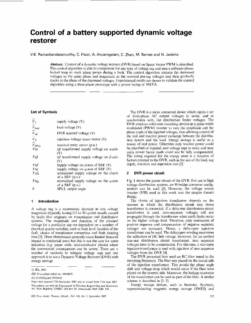
Fig. I shows the power circuit of the DVR. For use in high voltage distribution systems, an H-bridge converter config- uration can be used [3]. However, the voltage source inverter (VSI) used in this work was the simpler Graetz Bridge.
The choice of injection transformer depends on the manner in which the distribution circuit step down transfoimer is connected. lf a delta-star distribution circuit transformer is used: zero-sequence voltages will not propagate through the transfonner when earth faults occur on the higher voltage level. Therefore, only restoration of positive sequence and compensation of negative sequence voltages are necessary Hence, a delta-open injectioii transrormer can be used. The dekd/open winding maximises the utilisation of DC link voltage. However? for an earthed star-star distribution circuit transrormer, zero sequence voltages have to be compensated. For this case, a star-open injection transformer is used with injection of zero sequence voltages from the DVR 141.
The DVR presented here used an RC filter tuned to the switching frequency. The filter was placed on the circuit side of the injection transformer. This avoids the phase angle shift and voltage drop which would occur if the filter wcre placed on the inverter side. Moreover, the leakage reactance of the transfonner can be used 21s part of the filter. A similar scheme is described in [3, 51.
Energy storage devices, such as hatteries, flywhccls, superconducting magnetic energy storage (SMES) and
533
@-- power supply
feeder
Fig. 1 Power CIYCIIII of the DVR
other loads
bypass Switch fault deltaistar
distribution transformer
deltalopen injection
transformer
crowbar
.................................................... .......................................
supercapacitors, are required to provide real power to the load when large voltage sags occur. The DVR presented here used lead-acid batteries [h]. Lead-acid batteries provide rapid response for either charge or discharge, but the available energy depends on the discharge rate. The time- scales under consideration are typically in the order of hundreds of milliseconds. Typically the energy injected would he taken from the charge associated with the battery double-layer capacitance, i.e. the space charge around electrodes of a charged battery. Transient effects such as ‘coup-de-fouet’ can therefore be avoided. Further details can he found in [6].
When the DVR is in an idle condition. active power can he absorbed to charge the lead-acid batteries by introducing a small control angle between the load voltage vector and the source voltage vector. Simultaneously, the reactive power to maintain the voltage level at I .O p.u. at the load- side can be provided. The magnitude and power factor of the sensitive load together with this control angle determine the recharging current of the batteries [I.
As the DVR is a series connected device, it will pass the full load current as well as any fault currents due to downstream faults. The rating of the DVR inverter becomes the limiting factor for normal load current Rowing in the circuit side windings and reflected in the inverter side windings of the injection transformer. For line currents exceeding the inverter rating due to a fault downstream, a crowbar circuit is typically incorporated to bypass the inverter side of the injection transformer and so protcct the DVR power electronics.
3 Control techniques
The control technique adopted depends on the sensitivity of the load to the mamitude. DhaSe shift or waveshane of the
- __ A == 1- battery
OC link capacitor
i -
three-phase three-wire PWM inverter
dvnamic voltam restorer
consider the limitations of the DVR itself such as the voltage injection capability (converter and transfomier rating) and optimisation of the size of the energy store.
Compensation for voltage sags using a DVR can be performed using reactive and real power [5,9-1 I]. When the voltage injected is in quadrature with the current at the fundamental frequency, compensation functionally equiva- lent to that produced by a series capacitor is obtained [12]. For reactive power compensation, the supply voltage V s that can be boosted to a given load voltage is limited to:
-
where is the load power factor angle of the phase being considered [ I I]. As thc injcctcd voltage is in quadrature with the line current, a phase difference between the source and the load voltage will result. Hence, the magnitude of the injected voltage will be larger than when the source and the load voltages are in phase.
Although compcnsation using only reactive power allows the magnitude of the inverter output voltage to be varied continuously, it does not meet the requirements for dynamic compensation of disturbances that require real power transfer. In contrast, real power injection can he used to help boost the faulted supply voltages for a wider range of
Several control tcchniques have been proposed for loads [13].
compensation using real power injection [5, 9, IO]:
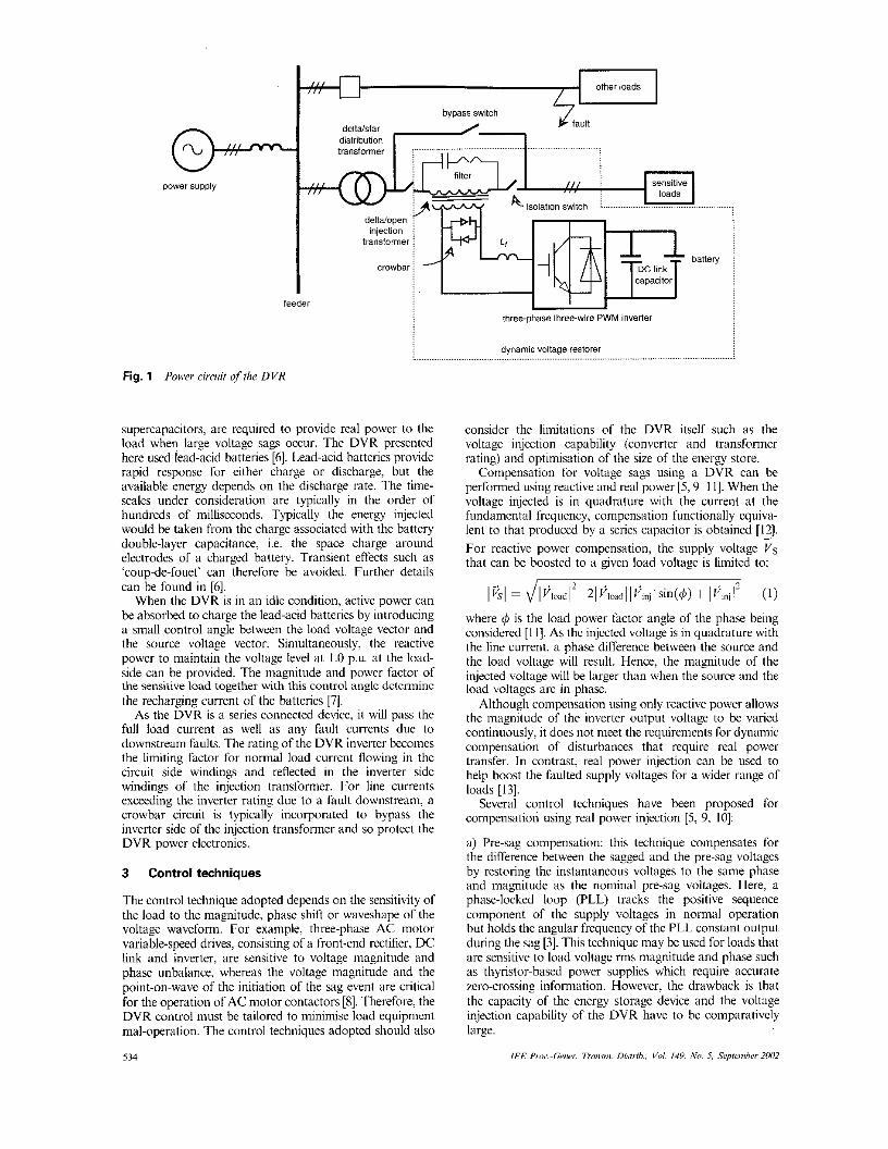
a) Pre-sag compensation: this technique compensates for the difference between the sagged and the pre-sag voltages by restoring the instantaneous voltages to the same phase and magnitude as the nominal pre-sag voltages. Here. a phase-locked loop (PLL) tracks the positive sequence comnonent of the supplv voltages in normal owration
voltage waveform: For example, three-phase AI? motor variable-speed drives, consisting of a front-end rectificr, DC link and inverter, are sensitive to voltage magnitude and phase unbalance. whereas the voltage magnitude and the point-on-wave of the initiation of the sag event are critical for the operation of AC motor contactors [8]. Therefore, the DVR control must be tailorcd to minimise load equipment mal-operation. The control techniques adopted should also
but holds the a n p l a r f&uency oTthc PLL constant output during the sag [3]. Tlus technique may he used for loads that are sensitive to load voltage rms magnitude and phase such as thyristor-based power supplies wluch require accurate zero-crossing information. However_ the drawback is that the capacity of the energy storage device and the voltage injection capability of the DVR have to he comparatively large.
534 IEE P r o . ~ G r , i n Trmswr. Dillrib., V d 149, h’o 5. Sepranher ZfK12
b) In-phase compensation: the restored voltages are in phase with the depressed source side voltages. thus minimising the magnitude of injected voltage. However, if the voltage sag is accompanied by a phase shift, the depressed source-side sag voltage will have a phase displacement with respect to the pre-sag voltage. This technique requires a fast tracking PLL. c) Energy optimisation technique: voltages are injected at a phase angle that will minimise the use of real power since voltage magnitude restoration is the only requirement. However, the injected voltages will be larger than for in- phase injection which increases the transformer and converter rating.
A number of DVR units have been put in commercial service. From the literature, it appears that one nianufac- turer [I6161 uses control method (c) with an over-current limit in some of their equipment. In other equipment [ I 1 a variety of in phase compensation is used to eliminate negativc sequence components and compensate for the deviation in positive sequence components. Another manufacturer [3, 18, 191 uses a phase-lock-loop in dq space to detect fiults and then hold constant the phase-lock-loop frequency: effectively pre-sag compensation.
The control technique presented here uscs lead-acid batteries for energy storage thus allowing flexibility of control. The technique restores the instantaneous load voltage to the same phase and magnitude as the nominal pre-sag voltage and then gradually changes the injected voltage to move the load voltage phasor angle towards the sagged voltage phasor angle as shown in Fig. 2. In this exaggerated example, immediately after the fault, the network voltage reduces in_magnitude and jumps some -45" (i.e. from VpR-lilp to Vs). This is compensated for by V,,. The PLL then tracks towards the network volt- age (V,) resulting in a reducing magnitude of injected
VS.3
Vsb v5q normalisation T3/2s vsc +
. .
n on troller
4
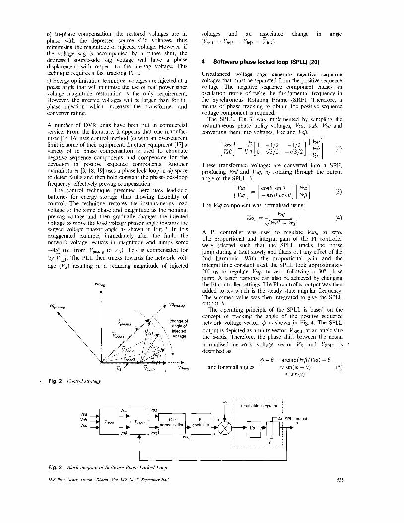
Unbalanced voltage sags generate negative sequence voltages that must be separated from the positive sequence voltage. The negative sequence component causes an oscillation ripple of twice the fundamental frequency in the Synchronous Rotating Frame (SRF). Therefore, a means of phase tracking to obtain the positive sequence voltage component is required.
The SPLL_ Fig. 3, was implemented by sampling the instantaneous phase utility voltages, Vsu, Vsb, Vsc and converting them into voltages, Vsm and Vsp.
Software phase locked loop (SPLL) I201
fia 2 1 -1/2 -1/2 [:;I =L[o J5/2 4 2 1
These transformed voltages are converted into a SRF, producing Vsd and Vsq, by rotating through the output angle of the SPLL, 0.
cos 9 sin H [E] =[-s in ,cosH][z ; ] (3)
The Vsq component was normalised using:
(4)
A PI controller was used to regulate Vsq,, to zero. The proportional and integral gain of the PI controller were selected such that the SPLL tracks the phase jump during a fault slowly and filters out any effect of the 2nd harmonic. With the proportional gain and the integral time constant used. the SPLL took approximately 200ms to regulate Vsq. to zero following a 30" phase jump. A faster response can also be achieved by changing the PI controller settings. The PI controller output was then added to o s which is the steady state angular frequency. The summed value was then integrated to give the SPLL
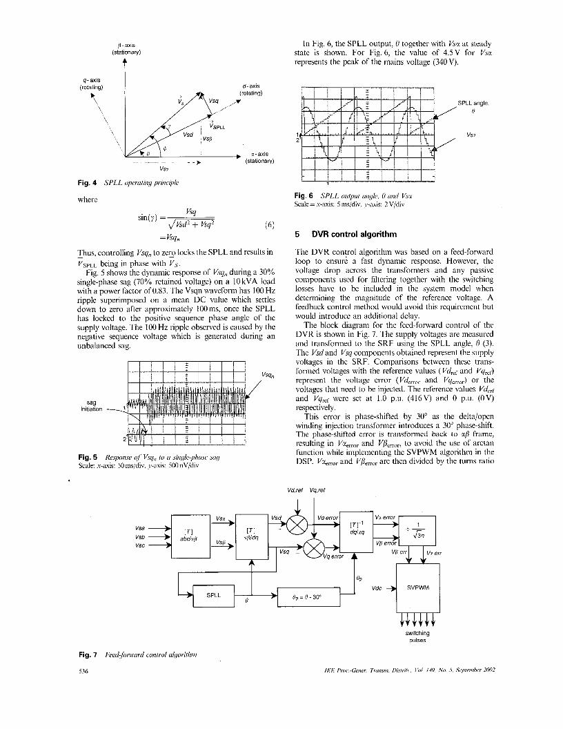
The operating principle of the SPLL is based on the concept of tracking the angle of the positive sequence network voltage vector_ 4, as shown_in Fig. 4. The SPLL output is depicted as a unity vector, VSPLL at an angle 0 to the a-axis. Therefore, the phase shift between th_e actual normalised network voltage vector V S and VSPLL is described as:
output, 9.
4 - s = arctan(fip/&a) - H
= sin(y) and for small angles zx sin(4, ~ 0) ( 5 )
835
q-axis (rotating) d-axis
b (rotating)
VS?
Fig. 4 SPLL oprur i iq principle
wherc
In Fig. 6, the SPLL output. 0 together with Vsa at steady state is shown. For Fig. 6, the value of 4.5V for Vsg represents the peak of the mains voltage (340V).
SPLL angle. 11
1 vs, 2
= &q.
Thus, controlling Vxlr, to ze? locks the SPLL and results in VsPLL being in phase with V S .
Fig. 5 shows the dynamic response of Vsq?,, during a 30% single-phase sag (70% retained voltage) on a 10 kVA load with a power factor of 0.83. The Vsqn wavefonn has 100 Hz ripple superimposed on a mean DC value which settles down to zero after approximately looms, once the SPLL has locked to the positive sequence phase anglc of the supply voltage. The 100 Hr ripple observed is caused by the negative sequence voltage which is generated during an unbalanced sag.
I j / / i l j / l ~
vsq" I . , .
I ! j i i ~ i /
sag initiation
5 DVR control algorithm
The DVR control algorithm was based on a feed-forward loop to ensure a fast dynamic response. However, the voltage drop across the transformers and any passive components used for filtering together with the switching losses have to bc included in the system model when determining the magnitude of the reference voltage. A feedback control method would avoid this rcquircment hut would introduce an additional delay.
The block diagram for the feed-forward control of the DVR is shown in Fig. 7. The supply voltages are measured and trnnsfonned to the SRF using the SPLL angle, B (3) . The Vsrland Vsq components obtained represent the supply vollages in the SRF. Comparisons between these trans- foimed voltages with the reference values ( V&[ and V&,) represent the voltage crror (Vderor and Vq,-rrur) or the voltages that need to he injected. The reference values V& and Vq,, were set at 1.0 p.u. (416V) and 0 p.u. (OV) respectively.
This error is phase-shifted by 30" as the delta/open winding iiiiection transfomier introduces a 30" uhase-shift. I . The phase-shifted crror is transfonned hack to e/? frame_ resulting in Vger.,,,, and V/lcnur. to avoid the use of arcran functioii while implementing the SVPWM algorithm in the DSP. Va,,,,,, and VpemOr are then divided by the turns ratio
Vd,ref Vq.ref
VS.S Vsb VSC
Solving (7) yields the following periods:
(9)
Equations (8) and (9) show the active switching period calculation for sector 1. Once f l and I? have been found, the total duration of the null voltage vector (1, and f7) during the sample interval is computed according to (IO) and ( I I )
Tn,,ll = % ~ / 2 - ti - 12
T,,"ii = to + 17 where 1" = f 7
(10)
(11) The apportioning of thc total null voltage vector time between f, and l7 csscntially controls the addition of
1.5.5 Pro;-Gcnw nrrw,i. IliriiW.. VoL 14Y. N o 5, Smmrrh<w 2fX12
common modc (triplen) haimonic components into the PWM waveforms. They however do not pass through a delta-open trmsfoimer connection.
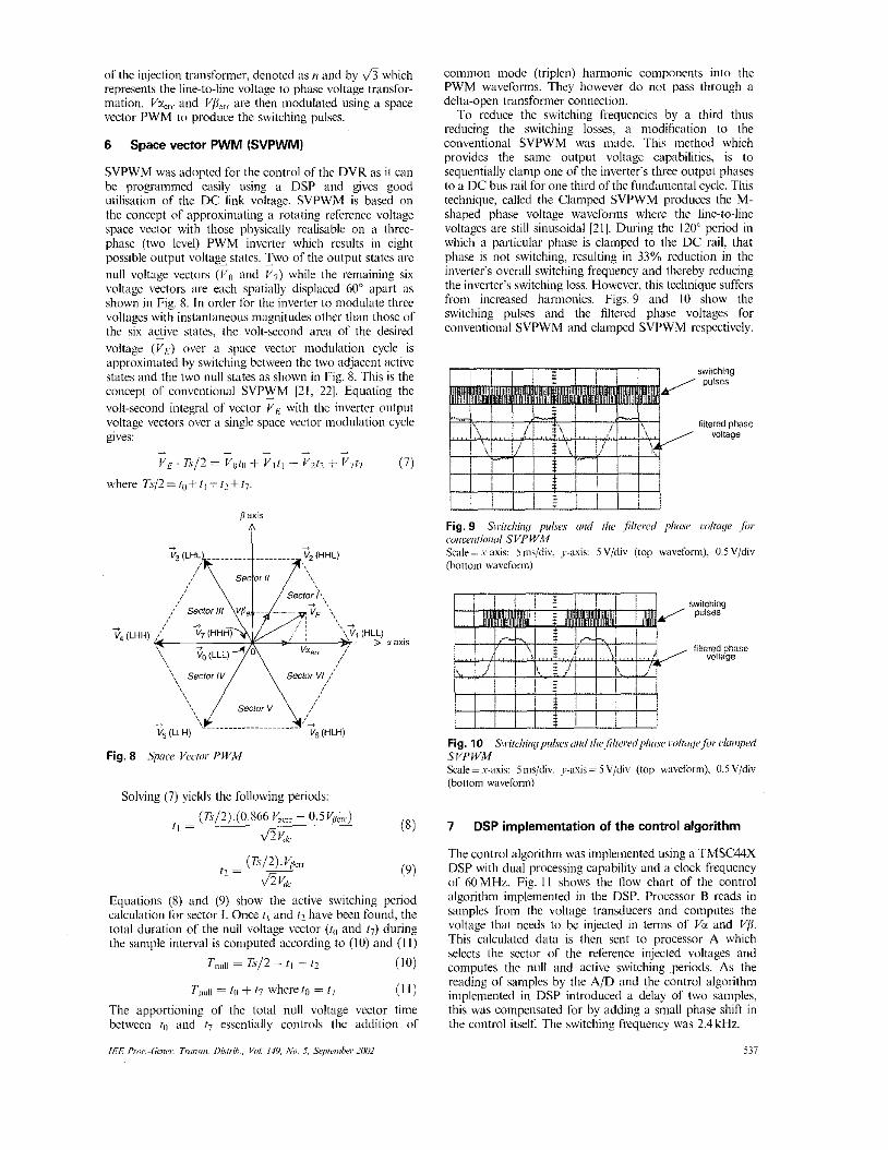
To reduce the switching hequencics by a third thus reducing the switching losses, a modification to the conventional SVPWM was made. This method which provides the samc output voltage capabilities. is to sequentially clamp one of the inverter's three output phases to a DC bus rail for one third of the fundamental cycle. This technique, called the Clamped SVPWM produces the M- shaped phase voltage waveforms where the line-to-line voltages are still sinusoidal [?I]. During the 120" period in which a particular phase is clamped to the DC rail_ that pliase is not switching. resulting i n 33% reduction in the inverter's ovcrall switching frequency and thereby reducing the inverter's switching loss. However, this technique suffers from increased harmonics. Figs. 9 and I O show the switching pulses end the filtered phase voltages for conventional SVPWM and clamped SVPWM respectively.
swiiching pulses
filtered phase "Ollage
/
I
Switching pulses
filtered phase w1iage
7
The control algorithm was implemented using a TMSC44X DSP with dual processing capability and a clock frequency of 60 MHz. Fig. 11 shows the flow chart of the control algorithm implemented in the DSP. Processor B reads in samples from the voltage transducers and computes the voltage that needs to be injected in ternis of Vu and Vfl. This calculated data is thcn sent to processor A which selects the sector of the reference injected voltages and computes the null and active switching yeiiods. As the reading of samples by the A/D and the control algorithm implemented in DSP introduced a delay of two samples, this was compensated for by adding a sinnll phase shift in the control itself. The switching frequency was 2.4kHz.
DSP implementation of the control algorithm
531
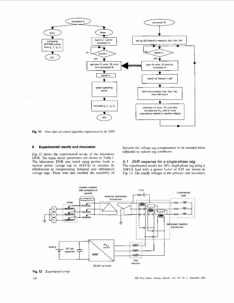
proocessor A processarB
1 handl=l. call for set up AID board to measure Vsa, Vsb. Vsc
processor B producing SVPWM pulses from b, tl, 4. t7
gwe vz error, VI? errorto p r o ~ e s ~ o i A
select operating
calculate b, t,, f2, t7 9 8 Experimental results and discussion
Fig. 12 shows the expenmental set-up of the hhoratory DVR. The main circuit parameters are shown in Table 1. The laboratory DVR was tested using passive loads at various power ratings (up to l0kVA) to examine its effectiveness in compensating halanced and unbalanced voltage sags. These tests also enabled the suitability of
Fig.
538
variable resistors with contactom in
Y - l handl=O, hand2=l call . read new samples Vsa, Vsb, Vsc
from AID board
includes the PLL and ali other calculations related lo injected voltage) .
batteries for voltage sag compensation to he assessed when subjected to various sag conditions.
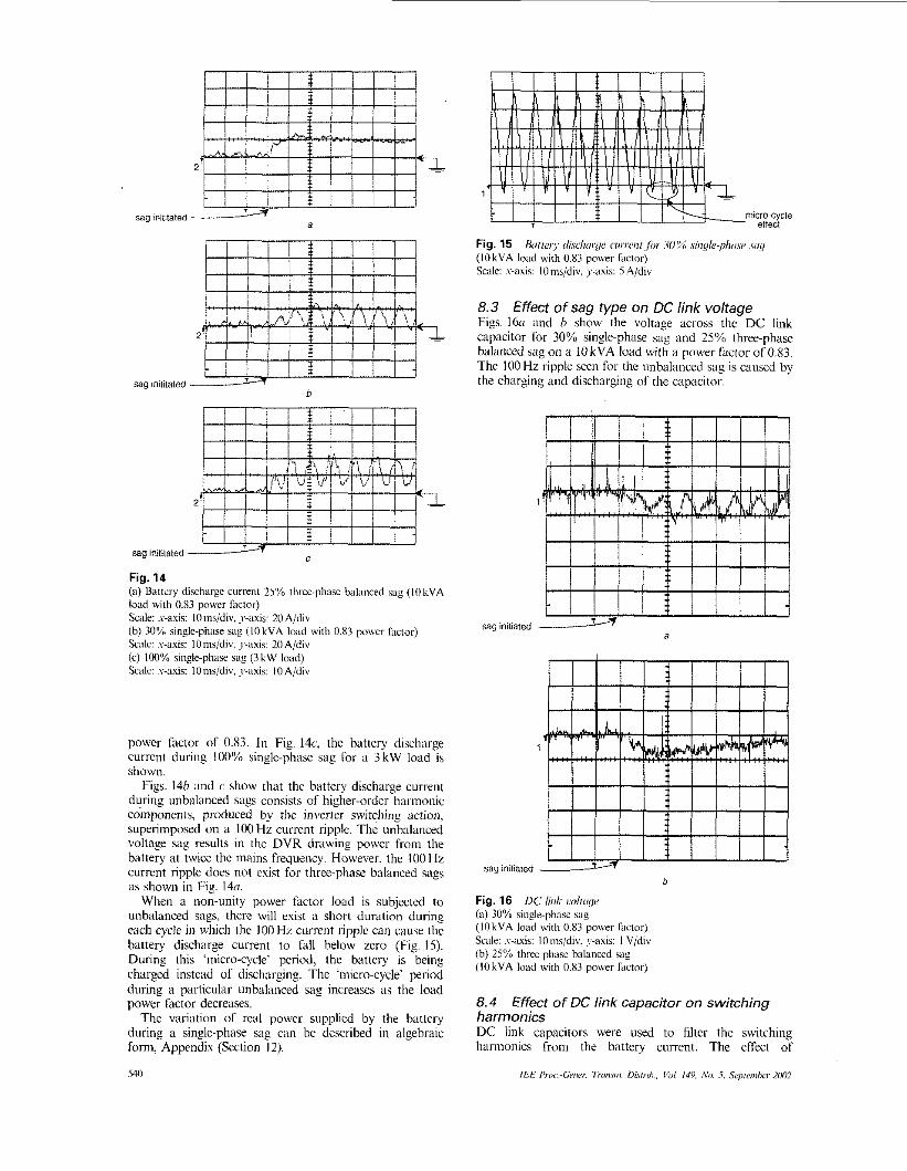
8.1 DVR response for a single-phase sag The experimental results for 30% single-phase sag using a IOkVA load with a power factor of 0.83 are shown in Fig. 13. The supply voltages at the primary and secondary
filter Y-connected
load
.. . . ...................................
inductor DClAC converler
12 Experbnenlal set-up
1.5.5 P m ~ G m e r . Tron.lni. Disrrih.. Vol. 14Y. N o 5, Sq~Imher 2W2
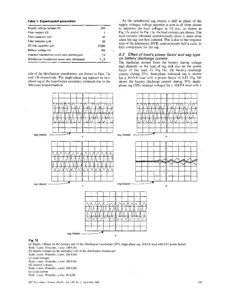
Table 1: Experimental parameters
Supply voltage (phase) (VI Filter resistor (R) Filter capacitor (pF)
Filter inductor (pH)
DC link capacitor (pFI
Battery voltage (V)
Injection transformer turns ratio (deltalopen)
Distribution transformer turns ratio (deltalstar)
240 1 47 50
27200 100 1:4
l:J3
side of the distribution transformer. are shown in Figs. 130 and 13h respectively. The single-phase sag appears as two- phase sag at the transformer secondary tennindls due to the delta/atar transformation.
sag initiated
AS the unbalanced sag. creates a shift in phase of the Supply voltages. voltage injection is seen in all three phases to maintain the load voltages at 1.0 p.u., as shown in Fig. I3c and d In Fig. 13e, the load currents are shown. The load currents obtained expenmcntally show a small drop when the sag was first initiated. This is due to the response time of the laboratory DVR, approximately half a cycle, to fully compensate for the sag.
8.2 . Effect of load's power factor and sag type on battery discharge current The discharge current from the battery during voltage sags depends on the type of sag and also on the power factor of the load. In Fig. 141, the battery discharge current during 25% three-phase balanced sag is shown for a IOkVA load with a power Factor of 0.83. Fig. 14h shows thc battery discharge current during 30% single- phase sag (70% retaincd voltage) for a I O kVA load with a
b sag initiated
sag initiated d
sag initialed / e
Fig. 13 (a) Supply voltages on the primary side of the distribution transformer (30% single-phase sag. 10 kVA load with 0.83 power factor) Scale: .~-aris: IOms/div. y-axis: 100 Vjdiv (b) Supply voltages on the secondary side of the distribution trensformcr %ale: .y-axis: IOms/div; y-axis: 200 V/div (c) Load voltages Scale: ~y-axis: 10 ms/div: y-axis: ZOO Vjdiv (d) lnjstcd voltagcs SCdk r-axis: I O ms/div: ~i,-axis: XKI V/div (e) Load current Scale: .y-axis: IOms/div: )-axis: I O A/div
IEE Pro.~Gewr. Tronsrz. Disirih.. Vol. 149, N o 5. Sqmnlm 2UU2 539
sag tnititated
sag iniiilaied b
sag inititated
Fig. 14 (a) Battery dirhergc current 2S% thrcc-phase balanced se3 (IOkVA load with 0.83 powci ficlar) Scale: .,--axis: IOms/div, J-anis: 20A/div (b) 30% singlc-phase sag ( I O kVA load with 0.83 powcr ?actor) Scalc: I-axis: lOms/div. y-axis: 2OA/div (c) IN)% single-phax sag (3 k W load) Scale: -Bxis: IOms/div, y-axis: I O A/div
c
power factor of 0.83. In Fig. 14c, the battery discharge current during 100% single-phase sag for a 3 kW load is shown.
Figs. 146 and c show that the battery discharge current during unbalanced sags consists of higher-order harmonic components, produced by the inverter switching action, superimposed on a 100 Hz current ripple. The unbalanced voltage sag results in the DVR drawing power from the battery at twice the mains frequency. However, the l00Hz current ripple does not cxist for three-phase balanced sags as shown in Fig. 140
When a non-unity power factor load is suhjected to unbakanced sags, there will exist a short duration during each cycle in which the 100Hz current ripplc can canse the battery discharge current to fall below zero (Fig. IS). During this 'micro-cycle' pcriod, the battery is being charged instead of discharging. The 'micro-cycle' period during a particular unbalanced sag increases as the load power Factor decreases.
The variation of real power supplicd by the battery during a single-phase sag can he described in algebraic Tom Appendix (Section 12).
S4U
1
micro-cycle effect
Fig. 15 fkrrto:,. d;.scl~orye ~ I I I W I I ~ / i r 3o'% .s;nqle-plz~~.~e . S U ~
.jcI. ,I e. .i-ms: . , ' IOms/div. y-axis: S A/div
8.3 Effect of sag type on DC link voltage Figs. 16rr and h show the voltage across the DC link capacitor for 30% single-phase sag and 25% three-phase baktnced sag on it I O kVA load with a pox'er Factor of 0.83. The 100 Hz iipple seen for the unbalanced sag is caused by the charging and discharging of the capacitor.
(IOkVA load with 0.83 pom'er Factor)
sag initiated
b
Fig. 16 DC link uolioge (:I) 30% single-phase sa8 (IOkVA h a d with 0.83 powr kictor)
(b) 25% three-phase balancced iag (IOkVA load with 0.83 power factor)
S C I . e. .\-~XS . , . I0nis/div. !;-anis: I V/div
8.4 harmonics DC link capacitors were used to filter the switching harmonics from the battery current. The effect of
Effect of DC link capacitor on switching
l l l t f + o . - G ~ w ~ w Tra" Dbirrh.. VoI 149, ,No 5. Sqrernhel- ?lM?
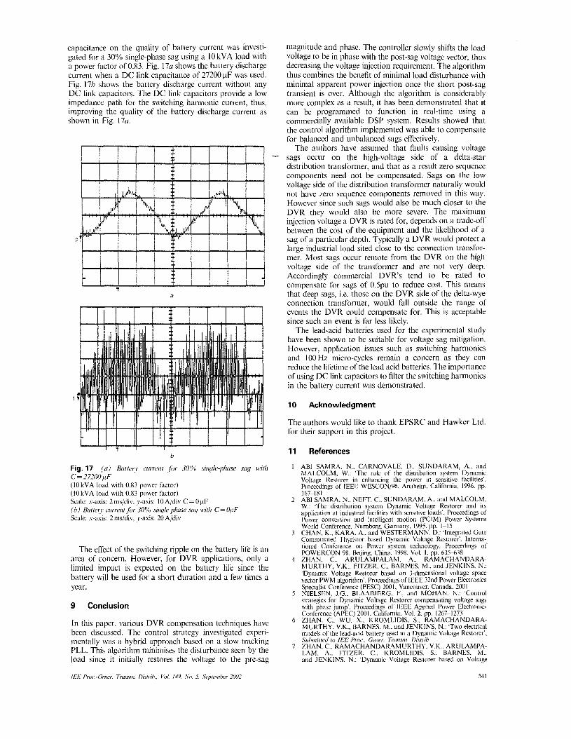
capacitance on the quality of battery current was invcsti- gated for a 30% single-phase sag using a 10 kVA load with a power factor of0.83. Fig. 170 shows the battery discharge cui-rent when a DC link capacitance of 27200pF was used. Fig. 17h shows the battcry discharge current without any DC link capacitors. The DC link capacitors provide ii low impedance path for the switching haimonic currcnt. thus, improving the quality of the battery discharge current as shown in Fig. 174.
a
1 1
The erect of the switching ripple on the battery life is an arca of concern. However. for DVR applications. only a limited impact is expected on the battery life since the battery will be used for a short duration and a few times a year.
9 Conclusion
In this paper. various DVR compensation techniques have been discussed. The control strategy investigated experi- mentally was a hybrid approach based on a slow tracking PLL. This algorithm minimises the disturbance secn by the load since it initially restores the voltage to the pre-sag
IEE Pruc.-Gwm Twism Di.sirih, I+,/ . 149. Y o 5, Scp,or&r 2002
magnitude and phase. The controller slowly shifts the load voltage to be in phase with the post-sag voltage vector, thus decreasing the voltage injection requirement. The algorithm thus combines the benefit of minimal load disturbance with minimal apparent power injection once the short post-sag transient is ovcr. Although the algorithm is considerably more complex as a result, it has been demonstrated that it can he programmed to function in real-time using a commercially available DSP system. Results showed that tlie control algorithm implemented was able to compensate for balanced and unbalanced sags effectively.
The authors have assumed that faults causing voltage sags occur on the high-voltage side of a delta-star distribution transfonner. and that as a result zero sequence components need not be compensated. Sags on the low voltage side or the distribution transformer naturally would not have zero sequence components removed in this way. Howevcr since such sags would also he much closer to the DVR they would also be more severe. The iilaxiniuin injection voltage a DVR is rated for_ depends on a tradc-off between tlie cost of the equipment and thc likelihood of a sag of a particular depth. Typically a DVR would protect a large industrial load sited close to the connection transfor- mer. Most sags occur remote from the DVR on the high voltage side of the transfonner and are not very deep. Accordingly commercial DVR's tend to be rated to compensate for sags of 0 . 5 ~ ~ to reduce cost. This means that deep sags. i.e. those on the DVR side of thc delta-\lye connection transformer. would fall outside the range of events the DVR could compensate for. This is acceptable since such an event is far less likely.
The lead-acid batteries used for the expeninental study have been shown to be suitable for voltage sag mitigation. However: application issues such as switching harmonics and 100Hz micro-cycles remain a concern as they can reduce the lifetime of the lead acid batteries. The importance of using DC link capacitors to filter tlie switching hannonics in the battery current was demonstrated.
10 Acknowledgment
The authors would like to thank EPSRC and Hawker Ltd. for their support in this project.
11
I
7
3
4
5
6
References
ABI SAMRA. N.. CARNOVALE. 9.. SUNDARAM. A.. alid MALCOLM, W.: 'The role of the distnbriliun system Dynilmlc V b h g e Restorer in cnhiincing the power ill xnsclive fxilities'. Procccdings of lEEE WESCONIYh. Anaheim. California. 1996. pp. 167-181 AB1 SAMRA. N.. NEFT C.. SUNIh\RAM. A,. ;tiid MALCOLM. w.: 'The distribution syslem Dynamic Voliage Restorer and ils applic;ition at induitriiil facilities with scmi~ive loads', Prccccdings of Power cmvcrsion and intcllim>t inmion (PCIMi Power Svslems World Conference. Numkrg.brmxiny. 1995. pp. '1-1 5 CHAN. K.. KARA. A,. and WESTERMANN. 0.: klegrated Gate Commutalrd Thvristor based Dynamic Vollnge Rrs to~r ' . Inlcme- lional Conferen& uti Power S Y Y ~ L ) ~ technolow. Proceedings of POWERCON 98. Beijing, China: 1998. Vol. 1. G. h l M 3 8 ZHAN, C.. ARULAMPALAM. A,. RAMACHANDARA- MURTHY. V.K.. FITZER. C.. RARNES. M.. and JENKINS. N.: 'Dyn;imic Voliiige Restom based on 3-dimensional vollage spxc v e m i PWM algonihm'. P m d i n g s af IEEE 32nd Power Electronics Smialirt Conference IPESQ 2CHIl. Vancouver. Canada. 20U I ~ I E L S E N . J.G.. BLAAB.IERG. F.. MOHAN. N.: . C O ~ O I stmir'es far Dynamic Voltage Restorer compsat ing voltage sags with phiirr jump'. Proccrdines of IEEE Applied Power Elcctroonics Confemce (APEC) 2001. C;kmin. Vol. 2. pp. 1267-1273 ZHAN. C.. WU. X.. KROMLIDIS. S.. RAMACHANUARA- MURTHY. V.K.. BARNES. M.. atid IENKINS. N.: 'Two electrical models of the lead-acid battery used 111 B Dynamic Vollage Restomcr'. S h m i i i d !u IEE Pro<.. Gmcr. Trwini. Di.swih ZHAN. C.. RAMACHANDARAMURIHY. V.K.. ARULAMPA- LAM, A,. FITZER. C.. KROMLIDIS. S.. BARNES. M.. and JENKINS. N.: 'Dynamic Voltage Rcslorw hitared on Vollage
541
Space Vector PWM control'. P r d i n @ of IEEE Applied Power Electronics Confcrmm (APEC) 2001. Califoomra. Vol. 2. pp. 1301-1307
x MIDDLEKAUFF, S.W.. ;rind COLLINS. E.R.: 'System and C U E L O ~ C ~ impact: considerations fbr senrs custom power dcvices', IEEE Tmnr Pouilrr Ddit,.. 1998. 13. (I), pp. 278-782 CHOI. S.S.. LI. B.H.. and VILATHGAMUWA. D.M.: 'Dynamic 9 Voltare Rcstoration with minimum energy injection'. I E E d TWLI. P o w ~ S w i . . 2000. 15. ( I ) . pp. 51-57
10 CHANC. C.S.. YANG, S.W.. and HO. Y.S.: 'Simulation and
Singaporr~2000, Vol. 4. pp. 247(;?481 II HEYDT. G.T.. TAN, W.. LAROSE, T., and NEGLEY. M.:
'Simulatimi and analysis of series voltagc hoost technology for power quality enhancement'. IFEE T,r,ni. Poww D<dir., 1998. 13. (4). pp.
Power En&n&ng Cbn&rcncc. Sineapore. ZOOl. pp. 432437 17 WEINHOLD. M., VOSS. L.. and ZUROWSKI. R.: 'Mcthod
and dwim for improving the quality of voltage on n secondary supply unit'. Siemens AG, Europcm Patent No. DE19737590. I "0"
~~~~ ~~~~, and Quality of Po&, IEEE, Athens. G~CKC. 1998, Vol. 1 . pp. 561-565 WUNDEKLIN. T.. DAHLER, P.. AMHOF, D.. and GRUNING. H.: 'Powcr supply quality improvement. with a Dynamic Voltage Restow (DVR)', Promdings of lntematioiial Conference on Energy management and powr delivery. IEEE. Singapore, 1998. Vol. 2, pp. 518-525 ZHAN. C.. FITZER. C.. RAMACHANDARAMURTHY. V.K.. ARULAMPALAM. A,. BARNES. M.. and JENKINS, N.: 'Soft- ware Phase-lmkd Loop applicd to a Dynamic Voltagc Restorer (DVR)'. Proceedings of IEEE Power Engineering Society Winter
19
20
Meeting 2001. ColGnhus. Ohio, USA BOYS. J.T.. and HANDLEY, P.G.: 'Harmonic an;ilysis of Space V e t o r Modulatd PWM wavefobnns'. IEE Pruc. 0. E k ~ l r . Powr A l p . . 1990, 137. (4). pp. 197-2-2M
22 BROECK, H.W.. SKUDELNY. H.C.. and STANKE. G.V.: .Analysis and realization of a pulsewidth modulator hased on Voltage Spam Vcnori'. IEEE Tram h d Appl.. 19x8. 24. ( I ) . pp. 142-150
21
12 Appendix
12.1 Power injected by DVR during a single- phase sag
K, = V,, COS W f = In, CoS(wt - $)
I$ = V", cos(wr - 120") l b = In, cos(wr - 120" - &) s = i . V, cos(wf - 240") IC = In, cos(wt - 240O" - 9) where I represents voltage reduction.
Total imtantaneouv poweroevfuom supply (P) P = V, ' I * + l$, ' rb + s ' I C
+ cos(wr - 120") ' cos(ut - 120" - 41)
P=V~,l,{coswt'cos(wt- &)
+ 1.. cos(wf - 240"). cos(w/ - 24V - $)}
KIJII,
2 + cos(2ot - 240" - 4) + icos(2wt - 120" - 9))
P = - { ( 2 + ; ~ ) c o s $ + c O s ( 2 w t - ~ )
VI L, 2
+ i cos(2wr - 120" - $)}
P = - { ( 2 + 1 ) .cosf/l -cos(2wt - 120" - $)
KJ," 2
+ (i - I ) . cos(2wr - 120" - $)]
P = - { ( 2 + 1.) . cos&
12.2 Instantaneous power supplied by the DVR (PDVR)
K A 2
P ~ ~ ~ ~ - ' ( l - i . ) . { c O s $ + c O s ( 2 w f - 120"-4)}
542
Copyright © 2022 FDOKUMEN