
Exploiting the dynamic Sn diffusion from deformation of FTO to boost the photocurrent performance of...
9
Exploiting the dynamic Sn diffusion from deformation of FTO to boost the photocurrent performance of hematite photoanodes Pravin S. Shinde a,b , Alagappan Annamalai a , Ju Hun Kim b , Sun Hee Choi c , Jae Sung Lee b,n , Jum Suk Jang a,nn a Division of Biotechnology, Advanced Institute of Environmental and Bioscience, College of Environmental and Bioresource Sciences, Chonbuk National University, Iksan 570-752, Republic of Korea b School of Energy and Chemical Engineering, Ulsan National Institute of Science and Technology (UNIST), 50 UNIST-gil, Ulsan 689-798, Republic of Korea c Pohang Accelerator Laboratory (PAL), Pohang University of Science and Technology (POSTECH), Pohang 790-784, Republic of Korea article info Article history: Received 16 March 2015 Received in revised form 18 April 2015 Accepted 12 May 2015 Available online 31 May 2015 Keywords: Hematite Onset potential Sn diffusion doping FTO conductivity Photoelectrochemical water oxidation abstract Herein, we report on exploiting effective Sn diffusion from the underlying FTO (F:SnO 2 ) substrate during post-growth annealing treatment to boost the photocurrent performance of α-Fe 2 O 3 photoanodes. Conventionally, hematite photoanodes are activated at high temperature (800 °C 4T 4650 °C) after initial low temperature annealing. The purpose of such activation is to utilize the diffusion of Sn ions leached from FTO deformation for improving the electronic conductivity and hence the photocurrent response of hematite photoanodes. However, the pre-formed oxide layer (in the first annealing) on the surface of FTO creates obstacle for diffusion of Sn ions during FTO deformation. To overcome this diffi- culty and to exploit Sn diffusion, we employed a direct single-step annealing of as-grown iron-coated FTO electrodes at 800 °C for short duration followed by quenching in air. Such activation greatly improved the water oxidation photocurrent response of hematite by 37% on account of increased Sn diffusion which was confirmed from X-ray photoelectron spectroscopy. Moreover, the onset of photo- current is shifted cathodically meaning that the water oxidation reaction proceeds at lower applied bias. Higher Sn content increased the electron donor concentration and hence improved the charge transfer kinetics of hematite as studied from EIS and Mott–Schottky measurements. Interestingly, despite higher Sn diffusion, the loss of FTO conductivity was minimal and the structural ordering was highest in one- step-activated hematite compared to conventionally activated hematite photoanodes as studied from XAFS analysis. & 2015 Elsevier B.V. All rights reserved. 1. Introduction Hematite (α-Fe 2 O 3 ) is widely studied for photoelectrochemical (PEC) water splitting due to its favorable band gap (E g 2.1 eV), maximum theoretical efficiency (12.9%), good electrochemical stability, abundance, non-toxicity, and cost-effectiveness [1,2]. However, its PEC activity is limited by ultra-fast charge recombi- nation (τ 10 ps), small hole diffusion length (2–4 nm), and poor carrier mobility (0.2 cm 2 V 1 s 1 ) [3,4]. The PEC activity can be improved by increasing the charge carrier density via intentional or unintentional doping [1,4,5], by increasing the hematite–elec- trolyte interface area via engineering nanostructure morphology [2,6,7], and by reducing the over-potential via surface treatments [7–9]. Annealing is one of the influential parameters that decide the physico-chemical properties of hematite. The photoactivity of hematite fabricated on FTO (F:SnO 2 ) substrate at low temperature is very poor and requires a thermal activation at high tempera- tures (650–800 °C) to induce Sn doping from FTO for improvement [3,10]. Conventionally, hematite is activated for efficient PEC per- formance via two-step heat treatment that involves initial low- temperature heat treatment at 500–550 °C for 2–10 h and natural cooling until room temperature, followed by high-temperature annealing at 800 °C for 10–20 min [3,7,11,12]. The purpose of low- temperature heat treatment for synthesis of hematite electrodes by different methods such as colloidal, doctor-blade, hydrothermal and sputtering was reported to be for removing the organics, bringing about the nanostructured growth and particle con- nectivity. The improvement in photoactivity due to high-tem- perature annealing was mainly attributed to the n-type doping of Sn cations diffused from the deformed FTO substrate. Such cationic Contents lists available at ScienceDirect journal homepage: www.elsevier.com/locate/solmat Solar Energy Materials & Solar Cells http://dx.doi.org/10.1016/j.solmat.2015.05.020 0927-0248/& 2015 Elsevier B.V. All rights reserved. n Corresponding author. Tel.: þ82 52 217 2544. nn Corresponding author. Tel.: þ82 63 850 0846; fax: þ82 63 850 0834. E-mail addresses: [email protected] (J.S. Lee), [email protected] (J.S. Jang). Solar Energy Materials & Solar Cells 141 (2015) 71–79
Transcript of Exploiting the dynamic Sn diffusion from deformation of FTO to boost the photocurrent performance of...
Solar Energy Materials & Solar Cells 141 (2015) 71–79
Contents lists available at ScienceDirect
Solar Energy Materials & Solar Cells
http://d0927-02
n Corrnn CorE-m
journal homepage: www.elsevier.com/locate/solmat
Exploiting the dynamic Sn diffusion from deformation of FTO to boostthe photocurrent performance of hematite photoanodes
Pravin S. Shinde a,b, Alagappan Annamalai a, Ju Hun Kim b, Sun Hee Choi c, Jae Sung Lee b,n,Jum Suk Jang a,nn
a Division of Biotechnology, Advanced Institute of Environmental and Bioscience, College of Environmental and Bioresource Sciences, Chonbuk NationalUniversity, Iksan 570-752, Republic of Koreab School of Energy and Chemical Engineering, Ulsan National Institute of Science and Technology (UNIST), 50 UNIST-gil, Ulsan 689-798, Republic of Koreac Pohang Accelerator Laboratory (PAL), Pohang University of Science and Technology (POSTECH), Pohang 790-784, Republic of Korea
a r t i c l e i n f o
Article history:Received 16 March 2015Received in revised form18 April 2015Accepted 12 May 2015Available online 31 May 2015
Keywords:HematiteOnset potentialSn diffusion dopingFTO conductivityPhotoelectrochemical water oxidation
x.doi.org/10.1016/j.solmat.2015.05.02048/& 2015 Elsevier B.V. All rights reserved.
esponding author. Tel.: þ82 52 217 2544.responding author. Tel.: þ82 63 850 0846; faail addresses: [email protected] (J.S. Lee), ja
a b s t r a c t
Herein, we report on exploiting effective Sn diffusion from the underlying FTO (F:SnO2) substrate duringpost-growth annealing treatment to boost the photocurrent performance of α-Fe2O3 photoanodes.Conventionally, hematite photoanodes are activated at high temperature (800 °C4T4650 °C) afterinitial low temperature annealing. The purpose of such activation is to utilize the diffusion of Sn ionsleached from FTO deformation for improving the electronic conductivity and hence the photocurrentresponse of hematite photoanodes. However, the pre-formed oxide layer (in the first annealing) on thesurface of FTO creates obstacle for diffusion of Sn ions during FTO deformation. To overcome this diffi-culty and to exploit Sn diffusion, we employed a direct single-step annealing of as-grown iron-coatedFTO electrodes at 800 °C for short duration followed by quenching in air. Such activation greatlyimproved the water oxidation photocurrent response of hematite by 37% on account of increased Sndiffusion which was confirmed from X-ray photoelectron spectroscopy. Moreover, the onset of photo-current is shifted cathodically meaning that the water oxidation reaction proceeds at lower applied bias.Higher Sn content increased the electron donor concentration and hence improved the charge transferkinetics of hematite as studied from EIS and Mott–Schottky measurements. Interestingly, despite higherSn diffusion, the loss of FTO conductivity was minimal and the structural ordering was highest in one-step-activated hematite compared to conventionally activated hematite photoanodes as studied fromXAFS analysis.
& 2015 Elsevier B.V. All rights reserved.
1. Introduction
Hematite (α-Fe2O3) is widely studied for photoelectrochemical(PEC) water splitting due to its favorable band gap (Eg�2.1 eV),maximum theoretical efficiency (12.9%), good electrochemicalstability, abundance, non-toxicity, and cost-effectiveness [1,2].However, its PEC activity is limited by ultra-fast charge recombi-nation (τ�10 ps), small hole diffusion length (2–4 nm), and poorcarrier mobility (0.2 cm2 V�1 s�1) [3,4]. The PEC activity can beimproved by increasing the charge carrier density via intentionalor unintentional doping [1,4,5], by increasing the hematite–elec-trolyte interface area via engineering nanostructure morphology[2,6,7], and by reducing the over-potential via surface treatments
x: þ82 63 850 [email protected] (J.S. Jang).
[7–9]. Annealing is one of the influential parameters that decidethe physico-chemical properties of hematite. The photoactivity ofhematite fabricated on FTO (F:SnO2) substrate at low temperatureis very poor and requires a thermal activation at high tempera-tures (650–800 °C) to induce Sn doping from FTO for improvement[3,10]. Conventionally, hematite is activated for efficient PEC per-formance via two-step heat treatment that involves initial low-temperature heat treatment at 500–550 °C for 2–10 h and naturalcooling until room temperature, followed by high-temperatureannealing at 800 °C for 10–20 min [3,7,11,12]. The purpose of low-temperature heat treatment for synthesis of hematite electrodesby different methods such as colloidal, doctor-blade, hydrothermaland sputtering was reported to be for removing the organics,bringing about the nanostructured growth and particle con-nectivity. The improvement in photoactivity due to high-tem-perature annealing was mainly attributed to the n-type doping ofSn cations diffused from the deformed FTO substrate. Such cationic

P.S. Shinde et al. / Solar Energy Materials & Solar Cells 141 (2015) 71–7972
incorporation dramatically decreases the resistivity of the film as aresult of enhanced donor density, thus positively affecting thephotoactivity of the photoanodes. However there are two decisivefactors that may limit the photoactivity of hematite. One is beha-vior of FTO conductivity during two-step annealing and another isformation of oxide layer during the first low-temperatureannealing. As FTO's role is to efficiently drive the photo-generatedelectrons to the back contact, maintaining its conductivity tooptimum level is crucial during high-temperature annealing. Wenoticed that the loss of conductivity in FTO is severe for thehematite photoanodes fabricated by conventional annealingapproach as a result of more FTO deformation due to longer hoursof processing time. The pre-formed oxide layer at the interface ofFTO may also pose interference for the dynamic diffusion of Snions during re-crystallization of hematite lattice at high-tem-perature annealing. Importantly, the Sn ions leached during FTOdeformation have to diffuse into the hematite lattice in a dynamicway so that the structural ordering of hematite is unperturbed.Therefore, there is a need to maintain a trade-off between theamount of Sn ions leached from FTO and minimum loss in con-ductivity of FTO. To overcome this difficulty, we used a direct one-step activation of hematite using as-grown iron-coated FTO elec-trodes at high temperature for optimum duration followed by amild quenching in air. Such heat treatment not only enables thecost-effective synthesis of hematite but also yields improved PECperformance.
In this work, it is demonstrated that different post-growthannealing conditions can significantly influence the photocurrentresponse of hematite photoanodes. We report on efficient utili-zation of Sn diffusion from the underlying FTO (F:SnO2) substrateduring hematite activation from FTO deformation at high tem-perature (HT) to boost the photocurrent of α-Fe2O3 photoanodes.We used two different states of electrodes for hematite activation:As-grown Fe/FTO (one-step activation at HT) and Fe2O3/FTO (two-step activation at 550 °CþHT). The annealing temperature and thetime for HT activation of hematite were optimized systematicallyby means of photocurrent performance. The state of material to beannealed is found to affect the dynamics of Sn diffusion, electrontransport and the PEC performance of photoanodes. The effect ofSn diffusion into hematite matrix on the changes in donor densityof hematite, shift in onset potential of water oxidation, dete-rioration in FTO conductivity, and structural ordering are dis-cussed. The possible mechanism during hematite activation isdiscussed to understand annealing phenomena.
2. Experimental
2.1. Synthesis of α-Fe2O3 photoanodes
The iron films were grown on fluorine doped tin oxide (FTO,F:SnO2, 10–15 sq. cm�1)-coated glass substrates by a facile pulsereverse electrodeposition (PRED) method according to our pre-vious study [13]. The process parameters of PRED such as ampli-tude of square wave pulse, duty cycle, pulse period, and depositiontime were [10 V (�6/þ4 V)] 20%, 10 ms, and 45 s, respectively. Theas-grown samples were rinsed in deionized water and driedimmediately using nitrogen stream. For one-step annealing, theas-grown samples were inserted into the box furnace (whosetemperature was already attained to high temperature, viz.800 °C), soaked for desired duration, air-quenched for few secondsand then transferred to the oven at 100 °C for 10 min. Afterkeeping in oven for 10 min, the samples were taken out from theoven to ambient air for cooling down completely. By followingsuch mild air-quenching process, we avoid the breaking of high-temperature-annealed red-hot samples as well as maintain the
crystalline synthesis of hematite photoanodes. Several as-grownfilms under identical synthesis conditions were prepared by PREDto investigate the effects of annealing temperature and annealingtime. The as-grown films were reflecting and dark greyish in color.Initially, by keeping the annealing time fixed for 15 min, the ele-vated temperature for one-step annealing was varied from 700 to825 °C. In the next step, by choosing the optimized annealingtemperature, the annealing time was varied from 10 to 17.5 min todecide on the optimum growth time for improving the photo-catalytic activity of iron oxide. The annealing conditions of sam-ples (iron oxide thin films) in both cases were optimized by meansof their PEC performance. Later, to compare the PEC performanceof optimized one-step-annealed photoanodes, the representativetwo-step-annealed hematite photoanodes were also preparedunder identical conditions of elevated annealing temperature afterthe initial low temperature annealing treatment at 550 °C for 4 hfollowed by natural cooling to room temperature. All annealedfilms were reddish brown in color. Despite having little wrinkledsurface, one-step-annealed films were well-adherent and showedno signs of any degradation. Alternatively, FTO substrates werealso annealed along with hematite electrodes by low temperature,one-step and two-step annealing methods at representativeannealing conditions.
2.2. Characterization of α-Fe2O3 photoanodes
The as-grown iron or low-temperature annealed hematite andthe representative one-step and two-step-annealed hematitephotoanodes (those prepared with optimized conditions of ele-vated annealing temperature) were characterized further tounderstand their contribution toward enhancing the PEC perfor-mance. The structural analysis was performed using PANalytical X′pert Pro MPD diffractometer equipped with Cu Kα radiationsource (wavelength Kα1¼1.540598 Å and Kα2¼1.544426 Å)operated at 40 kV and 30 mA. The X-ray diffraction patterns wererecorded in the diffraction angle range of 20–80° with step size of0.0167° s�1 and dwell time of 50.165 s. The morphology of theα-Fe2O3 films was examined on Field Emission Scanning ElectronMicroscope (FESEM) (SUPRA 40VP, Carl Zeiss, Germany), equippedwith X-ray energy dispersive spectrometer (EDS). The chemicalstate and elemental quantification in the freshly synthesized ironoxide samples was performed using X-ray photoelectron spectro-scopy (XPS). The XPS analysis was performed on a Thermo Sci-entific XPS spectrometer equipped with a monochromatic Al KαX-ray source (hν¼1486.6 eV). Wide survey spectra (BindingEnergy, BE: 1200–0 eV) were recorded for the samples using theX-ray spot size of 400 mm at room temperature with an analyzerpass energy of 200 eV and energy step size of 1 eV. High resolutionspectra in the region of interest were acquired at the pass energyof 50 eV and step size of 0.1 eV. The calibration of the bindingenergy of the high resolution spectra of all the iron oxide sampleswas made by referring the maximum of the adventitious C 1scarbon peak at 284.8 eV. The processing of XPS data was per-formed with the help of an XPS Peak-fit program using Shirleybackground. The high-resolution XPS spectra were de-convolutedwith a least squares fitting routine provided within the software. Asymmetric Gaussian–Lorentzian product function was used toapproximate the line shapes of the fitting components. Rawexperimental data were used for analysis with no preliminarysmoothing. The cross-sectional scanning electron microscopicimages of one-step and two-step-annealed Fe2O3 samples wereprepared with a FEI Helios 450HP NanoLab dual-beam focused ionbeam (FIB) system using a gallium ion beam. The samples werepartly melted due to the high energy of FIB during the samplepreparation. It was difficult to obtain clear images at high mag-nification (150k). The elemental mapping of cross-sectional
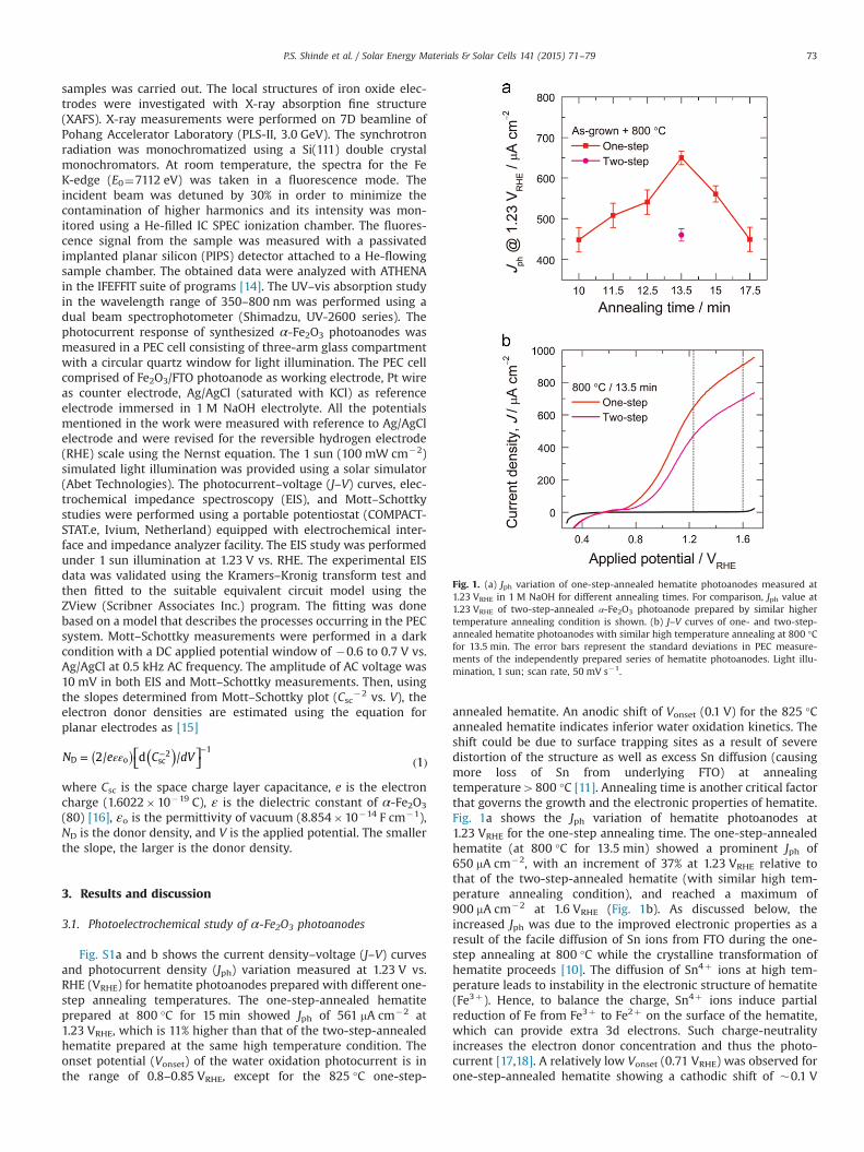
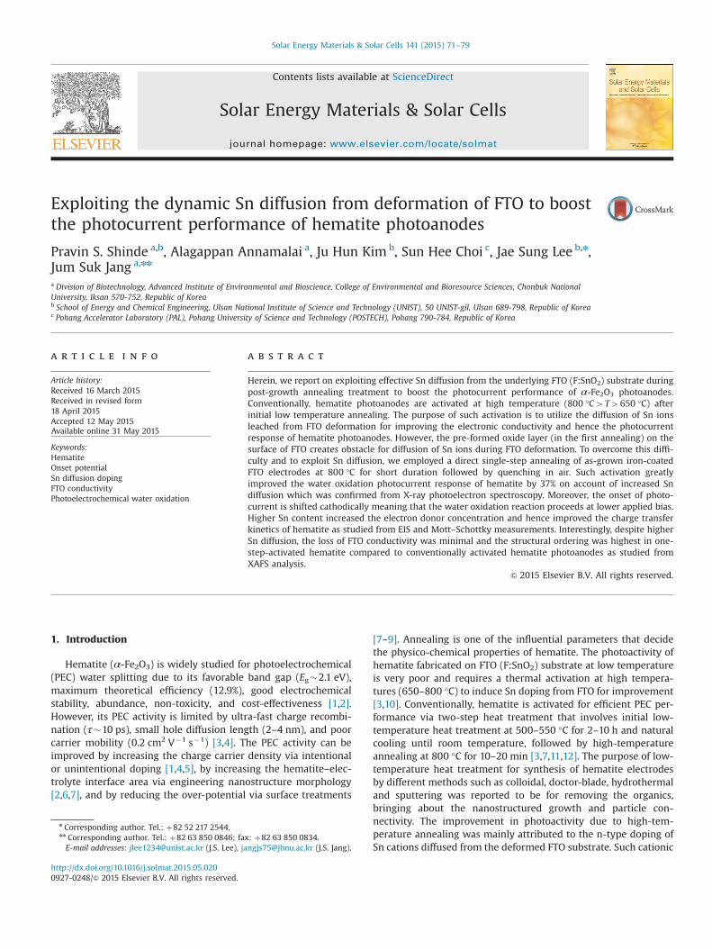
Fig. 1. (a) Jph variation of one-step-annealed hematite photoanodes measured at1.23 VRHE in 1 M NaOH for different annealing times. For comparison, Jph value at1.23 VRHE of two-step-annealed α-Fe2O3 photoanode prepared by similar highertemperature annealing condition is shown. (b) J–V curves of one- and two-step-annealed hematite photoanodes with similar high temperature annealing at 800 °Cfor 13.5 min. The error bars represent the standard deviations in PEC measure-ments of the independently prepared series of hematite photoanodes. Light illu-mination, 1 sun; scan rate, 50 mV s�1.
P.S. Shinde et al. / Solar Energy Materials & Solar Cells 141 (2015) 71–79 73
samples was carried out. The local structures of iron oxide elec-trodes were investigated with X-ray absorption fine structure(XAFS). X-ray measurements were performed on 7D beamline ofPohang Accelerator Laboratory (PLS-II, 3.0 GeV). The synchrotronradiation was monochromatized using a Si(111) double crystalmonochromators. At room temperature, the spectra for the FeK-edge (E0¼7112 eV) was taken in a fluorescence mode. Theincident beam was detuned by 30% in order to minimize thecontamination of higher harmonics and its intensity was mon-itored using a He-filled IC SPEC ionization chamber. The fluores-cence signal from the sample was measured with a passivatedimplanted planar silicon (PIPS) detector attached to a He-flowingsample chamber. The obtained data were analyzed with ATHENAin the IFEFFIT suite of programs [14]. The UV–vis absorption studyin the wavelength range of 350–800 nm was performed using adual beam spectrophotometer (Shimadzu, UV-2600 series). Thephotocurrent response of synthesized α-Fe2O3 photoanodes wasmeasured in a PEC cell consisting of three-arm glass compartmentwith a circular quartz window for light illumination. The PEC cellcomprised of Fe2O3/FTO photoanode as working electrode, Pt wireas counter electrode, Ag/AgCl (saturated with KCl) as referenceelectrode immersed in 1 M NaOH electrolyte. All the potentialsmentioned in the work were measured with reference to Ag/AgClelectrode and were revised for the reversible hydrogen electrode(RHE) scale using the Nernst equation. The 1 sun (100 mW cm�2)simulated light illumination was provided using a solar simulator(Abet Technologies). The photocurrent–voltage (J–V) curves, elec-trochemical impedance spectroscopy (EIS), and Mott–Schottkystudies were performed using a portable potentiostat (COMPACT-STAT.e, Ivium, Netherland) equipped with electrochemical inter-face and impedance analyzer facility. The EIS study was performedunder 1 sun illumination at 1.23 V vs. RHE. The experimental EISdata was validated using the Kramers–Kronig transform test andthen fitted to the suitable equivalent circuit model using theZView (Scribner Associates Inc.) program. The fitting was donebased on a model that describes the processes occurring in the PECsystem. Mott–Schottky measurements were performed in a darkcondition with a DC applied potential window of �0.6 to 0.7 V vs.Ag/AgCl at 0.5 kHz AC frequency. The amplitude of AC voltage was10 mV in both EIS and Mott–Schottky measurements. Then, usingthe slopes determined from Mott–Schottky plot (Csc�2 vs. V), theelectron donor densities are estimated using the equation forplanar electrodes as [15]
⎡⎣ ⎤⎦N e C dV2/ d / 1D o sc2 1( )( )εε= ( )
− −
where Csc is the space charge layer capacitance, e is the electroncharge (1.6022�10�19 C), ε is the dielectric constant of α-Fe2O3
(80) [16], εo is the permittivity of vacuum (8.854�10�14 F cm�1),ND is the donor density, and V is the applied potential. The smallerthe slope, the larger is the donor density.
3. Results and discussion
3.1. Photoelectrochemical study of α-Fe2O3 photoanodes
Fig. S1a and b shows the current density–voltage (J–V) curvesand photocurrent density (Jph) variation measured at 1.23 V vs.RHE (VRHE) for hematite photoanodes prepared with different one-step annealing temperatures. The one-step-annealed hematiteprepared at 800 °C for 15 min showed Jph of 561 mA cm�2 at1.23 VRHE, which is 11% higher than that of the two-step-annealedhematite prepared at the same high temperature condition. Theonset potential (Vonset) of the water oxidation photocurrent is inthe range of 0.8–0.85 VRHE, except for the 825 °C one-step-
annealed hematite. An anodic shift of Vonset (0.1 V) for the 825 °Cannealed hematite indicates inferior water oxidation kinetics. Theshift could be due to surface trapping sites as a result of severedistortion of the structure as well as excess Sn diffusion (causingmore loss of Sn from underlying FTO) at annealingtemperature4800 °C [11]. Annealing time is another critical factorthat governs the growth and the electronic properties of hematite.Fig. 1a shows the Jph variation of hematite photoanodes at1.23 VRHE for the one-step annealing time. The one-step-annealedhematite (at 800 °C for 13.5 min) showed a prominent Jph of650 mA cm�2, with an increment of 37% at 1.23 VRHE relative tothat of the two-step-annealed hematite (with similar high tem-perature annealing condition), and reached a maximum of900 mA cm�2 at 1.6 VRHE (Fig. 1b). As discussed below, theincreased Jph was due to the improved electronic properties as aresult of the facile diffusion of Sn ions from FTO during the one-step annealing at 800 °C while the crystalline transformation ofhematite proceeds [10]. The diffusion of Sn4þ ions at high tem-perature leads to instability in the electronic structure of hematite(Fe3þ). Hence, to balance the charge, Sn4þ ions induce partialreduction of Fe from Fe3þ to Fe2þ on the surface of the hematite,which can provide extra 3d electrons. Such charge-neutralityincreases the electron donor concentration and thus the photo-current [17,18]. A relatively low Vonset (0.71 VRHE) was observed forone-step-annealed hematite showing a cathodic shift of �0.1 V
P.S. Shinde et al. / Solar Energy Materials & Solar Cells 141 (2015) 71–7974
from typical values (0.8–1.0 VRHE) [3,5]. Ling et al. noticed similarshift for Sn-doped hematite electrodes and it was ascribed to bedue to the nature of synthesis method [4]. The much desiredcathodic shift in the onset potential observed for the one-stepannealed hematite is advantageous as the water oxidation reac-tions can proceed at a lower applied bias. This is a significantdevelopment in the context that several researchers utilized co-catalysts such as RuOx or cobalt-phosphate [5,19] to shift the onsetpotential of the water oxidation reaction. We achieve such shiftwith the help of modified annealing approach from underlyingFTO substrate without using any co-catalysts. Use of such co-cat-alysts led to decrease in onset potential at the expense of decreasein photocurrent response. The onset potential and photocurrent ofone-step activated hematite have the positive effects. This suggeststhat interfacial hole transfer is improved by reducing the deleter-ious carrier recombination processes. Fig. S2 shows the J–V curvesof one-step-annealed hematite photoanodes for all annealingtemperatures and annealing times. Next, the one- and two-step-annealed hematite photoanodes formed under similar high-tem-perature conditions (800 °C for 13.5 min) were further investi-gated to understand their structural, optical and electrochemicalproperties for photocurrent contribution.
3.2. XRD and FESEM studies
As shown in Fig. 2a, the as-grown film was in the form ofmetallic iron. Upon annealing at 800 °C (4550 °C) for 13.5 min,the iron film was transformed to a polycrystalline hematite(α-Fe2O3) phase having preferred growth along the (104) and (110)planes. The crystallite sizes determined from the high-intensitydiffraction peaks of two- and one-step-annealed hematite are ca.62 nm and 76 nm, respectively. Fig. 2b reveals the FESEM image ofas-grown iron film (�200 nm thick) deposited by PRED. The nano-structured growth and particle inter-connectivity during low-temperature annealing at 550 °C has been reported previously [13](Supporting information). In brief, the as-grown film consists ofagglomerated morphology with nanocrystalline clusters of
Fig. 2. (a) XRD patterns of as-grown iron film and two-step and one-step annealed hemhematite, and (d) one-step annealed hematite. Insets in Fig.4b and c show the correspo
spherical grains (30–50 nm). Upon low-temperature annealing at500 °C or 550 °C, the agglomerated clusters transform into amorphology that consists of compactly arranged nano-crystallinegrains with good inter-connectivity as seen from Fig. S3. Addi-tionally, the nano-rods as long as 400–700 nm and 50 nm in dia-meter also appear. The high-temperature annealing collapses thenanostructures and brings about further grain growth with dif-ferent size distributions as shown in Fig. 2c and d. The quality andsurface morphology of electrodes is almost similar for two-stepand one-step annealed hematite samples except the grain size. Ingeneral, two-step annealing produced smaller grains, which wasconsistent with the XRD study. Increased grain size (190 nm) inone-step annealing thus reduces the undesired grain boundarysites. Such a compact and interconnected morphology provideseasy and uninterrupted pathways for charge carriers to move tothe back contact, which in turn improves the photo-response.
3.3. XPS study
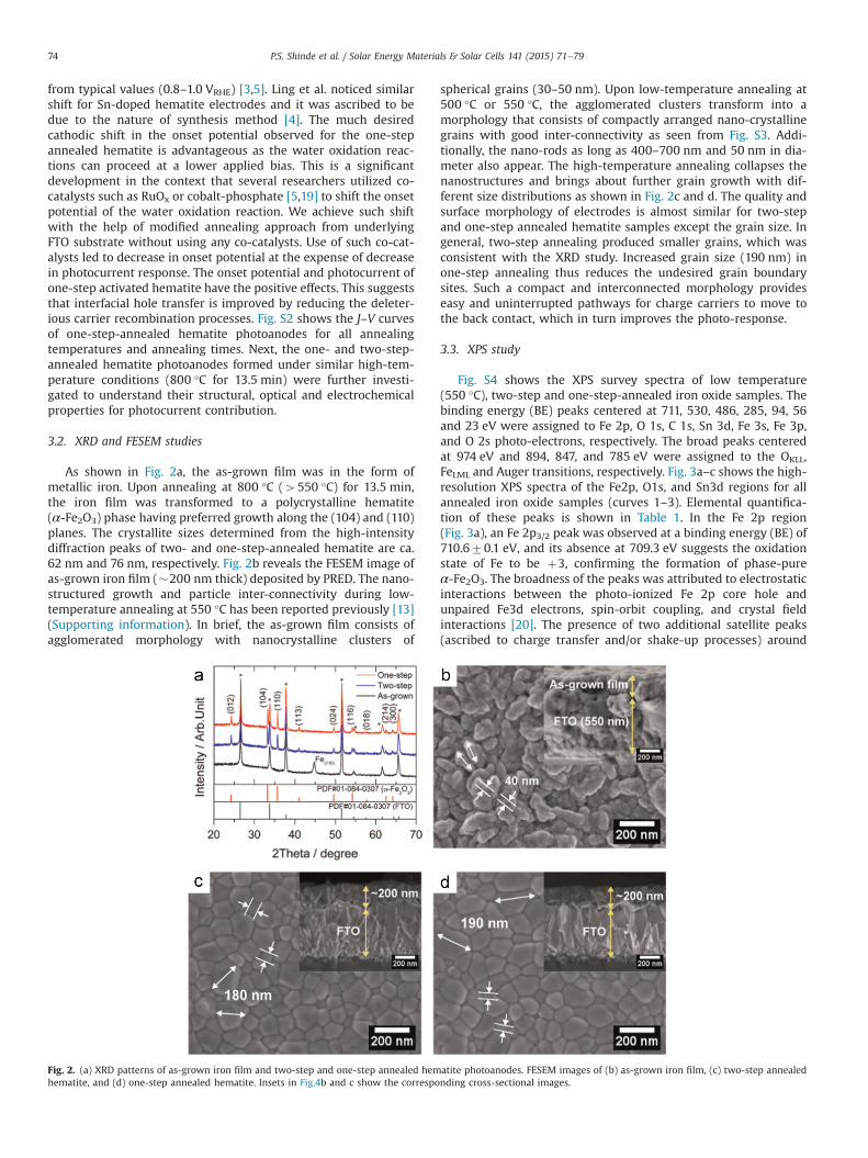
Fig. S4 shows the XPS survey spectra of low temperature(550 °C), two-step and one-step-annealed iron oxide samples. Thebinding energy (BE) peaks centered at 711, 530, 486, 285, 94, 56and 23 eV were assigned to Fe 2p, O 1s, C 1s, Sn 3d, Fe 3s, Fe 3p,and O 2s photo-electrons, respectively. The broad peaks centeredat 974 eV and 894, 847, and 785 eV were assigned to the OKLL,FeLML and Auger transitions, respectively. Fig. 3a–c shows the high-resolution XPS spectra of the Fe2p, O1s, and Sn3d regions for allannealed iron oxide samples (curves 1–3). Elemental quantifica-tion of these peaks is shown in Table 1. In the Fe 2p region(Fig. 3a), an Fe 2p3/2 peak was observed at a binding energy (BE) of710.670.1 eV, and its absence at 709.3 eV suggests the oxidationstate of Fe to be þ3, confirming the formation of phase-pureα-Fe2O3. The broadness of the peaks was attributed to electrostaticinteractions between the photo-ionized Fe 2p core hole andunpaired Fe3d electrons, spin-orbit coupling, and crystal fieldinteractions [20]. The presence of two additional satellite peaks(ascribed to charge transfer and/or shake-up processes) around
atite photoanodes. FESEM images of (b) as-grown iron film, (c) two-step annealednding cross-sectional images.

Fig. 3. High resolution XPS spectra of (a) Fe 2p, (b) O 1s, and (c) Sn 3d regions fordifferent iron (oxide) samples prepared on FTO substrate. Samples: (curve 1) lowtemperature annealing at 550 °C for 4 h, (curve 2) two-step annealing at 550 °Cfollowed by 800 °C, and (curve 3) one-step annealing at 800 °C.
Table 1The elemental ID and quantification of iron oxide films synthesized by PRED andannealed via low temperature (550 °C), two-step and one-step methods.
Peakelementsa
550 °C annealediron oxide
Two-step-annealediron oxide
One-step-annealediron oxide
Peak BE at% Peak BE at% Peak BE at%
Fe 2p 710.6 24.67 710.60 23.78 710.70 23.74O 1s 529.50 75.33 529.60 74.97 529.70 73.81Sn 3d5 – – 486.10 1.24 486.10 2.46
a Peak values were calibrated with reference to adventitious carbon at284.8 eV.
P.S. Shinde et al. / Solar Energy Materials & Solar Cells 141 (2015) 71–79 75
719 and 733 eV was consistent with the presence of α-Fe2O3
[20,21]. In O1s (Fig. 3b), the lowest BE peak centered around
Fig. 4. Cross-sectional scanning electron microscopic images of α-Fe2O3 photoanodes prrepresented by a dark-field scanning electron microscopy images at a magnification of 15melted due to the high energy of FIB during the sample preparation. (c) Schematic illus
530 eV was assigned to oxygen atoms in the iron oxide lattice, O 1s(Fe–O), and the peak around 531 eV to the lattice hydroxyl groups,O 1s(Fe–OH lattice) [20,22]. The O 1s(Fe–O) peak for the one-step-annealed sample is close to the ideal value (529.9 eV). However, aslight shift in its position toward lower BE for other samples couldbe due to a slightly disordered electronic structure of the Fe2O3.The shapes of the Fe 2p and O 1s spectra are similar to thosereported for α-Fe2O3 [23]. In Fig. 3c, the Sn 3d5/2 peak was absentat 486.10 eV for the 550 °C annealed sample, but appeared for bothtwo- and one-step-annealed samples. This suggests that, at ele-vated annealing temperatures, leaching and diffusion of tin (fromthe underlying FTO substrate) into the Fe2O3 matrix occurs, caus-ing electronic modification and changes in charge carrier density.Sn was reported to exist in hematite with a 4þ oxidation state.However, the appearance of an Sn 3d5/2 peak at slightly lower BE(486.1 eV) in the present study than that for SnO2
(�486.370.1 eV) could be related to oxygen deficiency. Theincreased Sn 3d5 peak intensity for the one-step-annealed sampleindicates a higher amount of diffused Sn content (ca. 2.46 at%)than that for the 2-step-annealed sample (ca. 1.24 at%). Hence, it isevident that the higher amount of diffused Sn in the one-step-annealed hematite improved its photocurrent. Such unintentionalSn doping in Fe2O3 is advantageous for improving photoactivity[24].
3.4. FIB study and schematic illustration
To assist the XPS study and to corroborate Sn diffusion phe-nomenon, the cross-sectional elemental mapping of one-step andtwo-step-annealed α-Fe2O3 photoanodes was carried out asshown in Fig. 4a and b. It is clear from these images that more Sn is
epared by (a) one-step and (b) two-step annealing method. The textured region is0k and corresponds to the elemental maps of Fe, Sn, and O. The samples were partlytration of growth mechanism during the one- and two-step annealing processes.

P.S. Shinde et al. / Solar Energy Materials & Solar Cells 141 (2015) 71–7976
diffused into the hematite matrix for one-step-annealed α-Fe2O3
photoanode. Fig. 4c shows the schematic illustration of the pro-posed growth mechanism of hematite during one- and two-stepannealing. Right before the hematite activation at 800 °C from FTOdeformation, the state of as-processed film is different in twoannealing processes—a metallic iron for one-step annealing (Fe/FTO) and a well-formed hematite at 550 °C for two-step annealing(Fe2O3/FTO). During second high-temperature annealing (800 °C),the pre-formed oxide layer in Fe2O3/FTO has to undergo re-crys-tallization and the Sn diffusion during re-crystallization of pre-formed oxide becomes difficult as this creates interference fordynamic migration of Sn ions. More FTO deformation is likely tooccur in two-step annealed samples as seen from the increasedseries resistance (sheet resistance of FTO). In contrast, duringhematite activation directly from Fe/FTO at 800 °C, the diffusion ofSn ions in semi-molten hot Fe mass is more favorable, resulting inSn enrichment in hematite. Although oxide formation rate ishigher during one-step annealing at high temperature, the diffu-sion of Sn ions occurs dynamically with minimal FTO deformationin comparison to the conventional two-step annealing approach.EIS spectra of one-and two-step annealed FTO substrates (Fig.6c)supports the above phenomena. Thus, hematite activation of as-grown Fe/FTO electrode by skipping intermediate low-tempera-ture heat-treatment greatly enriched the Sn cations into thehematite matrix to improve the electron donor concentrationwhile keeping the deformation of FTO to a minimal level. Suchactivation improved the water oxidation performance of hematitephotoanodes. These findings are well-supported by XPS and FIBanalysis.
3.5. XAFS study
The degree of crystallinity, defined as the ordering of thestructure, is an important factor determining the photoactivity of
Fig. 5. (a) Fe K-edge XANES spectra, (b) k2-weighted EXAFS functions, and (c) corresannealed iron oxide photoanodes.
the semiconductor because structural defects can act as recombi-nation centers. However, the XRD and XPS did not provide ampleclarification about the structural disorder in the hematite samples.Hence, to account for the structural disorder, the XANES andEXAFS studies were performed. Fig. 5a displays the Fe K-edgeXANES spectra of iron oxide photoanodes prepared with low-temperature (550 °C, LT550), one-step and two-step annealing.The spectra for all the samples were exactly the same as that of thereference α-Fe2O3, as evidenced from the observation of the pre-edge peak at 7115 eV denoting a quadrupole transition of 1s-3d.Moreover, the absorption rising feature and energy positions werealso the same. Although the XANES analysis revealed identicalelectronic local structure, the geometrical structure study fromEXAFS was different. In comparison with the reference α-Fe2O3,k2-weighted EXAFS function of one-step-annealed sample exhib-ited enhanced amplitude feature at 10–11 Å�1 (Fig. 5b). TheFourier transforms of corresponding samples are shown in Fig. 5c.The intensity of the first peak at 0.8–2.0 Å increased in a sequenceof α-Fe2O3otwo-step∼LT550oone-step. As the Fe–O coordina-tion number corresponding to interaction between the nearestneighbors and a central iron atom was invariant, the increase inthe intensity indicated the smaller Debye–Waller factor. TheDebye–Waller factor, indicator of the structural disorder, is a goodstructural parameter to elucidate the ordering of thin film. Thesecond peak at 2.1–3.9 Å consists of complicated Fe–Fe and Fe–Oscatterings (1 Fe–Fe at 2.90 Å, 3 Fe–Fe at 2.97 Å, 3 Fe–Fe at 3.36 Å,3 Fe–O at 3.40 Å, 3 Fe–O at 3.60 Å, 6 Fe–Fe at 3.70 Å, and 3 Fe–O at3.78 Å), thus revealing that each shell cannot be separated. Withthe enhanced EXAFS amplitude and the highest Fe–O peakintensity, it was concluded that the structural ordering was thehighest for the one-step-annealed hematite sample. This finding isconsistent with the XRD, FESEM and XPS results. It is important tonote that despite of higher Sn leaching from FTO deformation andtheir migration into the hematite lattice, the structural ordering inone-step-annealed hematite was maintained. This suggests that Sn
ponding Fourier transforms of low temperature (LT550), one-step, and two-step-

P.S. Shinde et al. / Solar Energy Materials & Solar Cells 141 (2015) 71–79 77
diffusion is unperturbed and dynamic. Conversely, pre-formedoxide layer in the case of two-step annealed hematite serves as abarrier for dynamic diffusion of Sn ions, and ultimately causesstructural disordering of hematite. Hence, the grain growth andthe improved crystallinity due to the structural ordering in one-step-annealed hematite together contributed to enhance thephotoactivity.
3.6. UV–vis spectroscopy
The understanding of light absorption properties in hematite isan important aspect that can provide important information onthe interactions of photocatalytic materials with photon energies,in order to choose the proper light to activate semiconductingmaterials for solar energy conversion. Fig. S5a and b shows theabsorbance (measure of absorbed photons) for one-step-annealedhematite photoanodes at representative annealing temperaturesand annealing times. Absorbance values at each wavelength wereincreased with high temperature annealing from 700 °C to 800 °Cbut decreased at 825 °C (Fig. S5a). The reduced absorbance couldbe due to excess diffusion of Sn ions into the hematite latticealtering the optical properties. No significant change was noticedin the absorbance for annealing time variation (Fig. S5b). Theabsorbance of one-step-annealed photoanodes was higher thanthat of two-step-annealed hematite at each wavelength as shownin Fig. S5c and also exhibited significant response at wavelengthsgreater than the band gap (�590 nm) due to scattering caused bythe large particles. Such scattering effect was lower in the two-step-annealed hematite due to lower grain size as evidenced fromFESEM study. The observation of our study is in accordance withthe literature in which it was demonstrated that the incorporation
Fig. 6. (a) Nyquist plots (under light) and (b) Mott–Schottky plot (under dark) of two- anthe equivalent circuit and the results of fitting. Inset of Fig. 6b shows the ND and Vfb valtwo-step (15 and 13.5 min)-annealed FTO electrodes. The Nyquist high frequency regionlight illumination was 100 mW cm�2 and the electrolyte was 1 M NaOH.
of Sn causes as large as 2-fold enhancement of optical absorptioncoefficient as a result of structural distortion of the hematite lattice[4]. Fig. S5d and e reveals the band gap energies (Eg) determinedfrom Tauc plots of two-step and one-step-annealed hematitephotoanodes. The Eg values for direct and indirect optical transi-tion are 2.13–2.14 eV and 2.11 eV, respectively, which are con-sistent with reported values [3,7].
3.7. EIS and MS study
The charge transfer characteristics of the hematite photo-anodes was studied by electrochemical impedance spectroscopy(EIS) at 1.23 VRHE. Fig. 6a shows the Nyquist plots (Z′ vs. �Z″) ofone-step and two-step-annealed α-Fe2O3 photoanodes that werefitted using Randles equivalent circuit [25]. The equivalent circuitelements include a series resistance (Rs), a space-charge capaci-tance of the bulk hematite (Cbulk), a surface state capacitance (Css),a resistance for trapping of holes in the surface states (Rtrap), and acharge transfer resistance from the surface states to solution(Rct,trap). Recently, the role of surface states in water splitting hasbeen of great interest. Surface states may mediate charge transferby performing a transit shipment of the photogenerated holes forthe oxidation reaction or provide recombination centers [25]. Thevalues of Rs and Rtrap for one-step-annealed hematite are con-siderably lower than that for two-step-annealed hematite. Nosignificant change in Cbulk is seen. A smaller Css means that thedensity of surface states responsible for recombination losses isrelatively lower. Css is slightly higher for one-step annealedhematite. This validates lower onset of photocurrent in one-step-annealed hematite. Importantly, lower Rct,trap in one-step annealedhematite surpasses the recombination losses. Hence, surface states
d one-step-annealed hematite photoanodes in 1 M NaOH. The inset of Fig. 6a showsues. (c) Nyquist plots (under light) of 550 °C (4 h), one-step (15 and 13.5 min), andis expanded in the inset. Inset shows the series resistance for all the electrodes. The

P.S. Shinde et al. / Solar Energy Materials & Solar Cells 141 (2015) 71–7978
associated with one-step-annealed hematite photoanodes mediatethe charge transfer.
The electron donor densities (ND) were estimated using theslopes from the linear fits of Csc�2 vs. V (Fig. 6b). The intercept oflinear fit to the voltage axis gives the flat band potential (Vfb) ofhematite. The ND value for one-step-annealed hematite(8.812�1019 cm�3) obtained from the plot is two times higherthan that of the two-step-annealed hematite (3.740�1019 cm�3).Consistent ND values in the range of 1018–1019 cm�3 were reportedfor high-temperature annealed hematite electrodes [4,12,26]. Theenhanced ND in one-step-annealed hematite can be directly rela-ted to the relatively higher amount of diffused Sn (as evidenced byXPS) from the underlying FTO without deteriorating its con-ductivity. The higher ND value reduces the depletion (spacecharge) layer thickness of the hematite, consequently leading tomore effective separation and transport of charge carriers sup-pressing the electron–hole recombination. The Vfb values for two-and one-step-annealed hematite were ca. 0.24 and 0.42 VRHE,respectively, suggesting that higher Sn doping in one-step-annealed hematite also promotes a significant anodic shift in Vfb
compared to the two-step-annealed hematite. The higher value ofVfb may be associated with Sn enrichment in the hematite grainsurface, which increases band-bending that in turn facilitates thecharge separation process. The Vfb is ideally equal to the photo-current onset potential (Vonset), but in practice it deviates fromVonset by an amount called an overpotential (to drive the water-splitting reaction). The greater shift in Vfb for two-step-annealedhematite can be related to increased surface trap resistance asevidenced from EIS, suggesting a high recombination rate andslow oxygen evolution kinetics at the hematite surface. Thisobservation can be validated from the smaller difference (0.29 V)in Vfb and Vonset for one-step-annealed hematite compared to thetwo-step-annealed hematite (0.54 VRHE). To validate the hypoth-esis of higher ND value on account of enriched Sn diffusion, EISstudy of FTO electrodes were carried out separately. Fig. 6c showsthe representative Nyquist plots (real vs. imaginary impedance) ofthe FTO electrodes prepared by low-temperature, one-step andtwo-step annealing methods, measured at a bias potential of1.23 VRHE under 1 sun illumination. The series resistance (Rs),which describes the total resistance from the contributions of FTO,electrical contacts, etc., was determined. The low-temperature-annealed (550 °C) hematite shows lowest value of Rs due to thefact that no loss of tin occurs because the Sn diffusion starts atannealing temperatures greater than 700 °C. Among the hightemperature annealed FTO electrodes, one-step-annealed FTO(800 °C for 13.5 min) exhibited lowest Rs value of 40.10Ω cm2,suggesting lower deterioration of conductivity in comparison tothat annealed by the two-step method. By this analogy, we con-clude that in the hematite–FTO system, the one-step annealing at800 °C for 13.5 min, in contrast to other studied annealing condi-tions, maintains the required FTO conductivity despite higheramount of Sn leaching. Thus, direct one-step activation of hematiteusing as-grown Fe/FTO via dynamic Sn cations diffusion from FTOdeformation can be an effective way to fabricate efficient photo-anodes for water oxidation reactions.
4. Conclusions
Hematite activation from FTO deformation at high temperature(viz. 800 °C) has been the choice of common practice to induce Sndoping in order to improve electronic conductivity and hence thePEC performance of hematite. This work introduces an effectiveway to exploit the dynamic diffusion of Sn ions leached duringhematite activation from FTO deformation at 800 °C for 13.5 minby avoiding an intermediate low-temperature annealing step
commonly employed for conventional approach. Such activationallows dynamic diffusion of Sn cations while preserving the opti-mum conductivity of FTO necessary for efficient charge collectionas well as maintains the highest structural ordering. In contrast, apre-formed oxide layer at the interface of FTO during intermediatelow-temperature annealing created interference for dynamic Sndiffusion. Moreover, these photoanodes suffer from the structuraldisordering during re-crystallization of pre-formed oxide layer andmore loss of FTO conductivity possibly due to longer hours ofprocessing time. Hence, the increased electron donor concentra-tion due to controlled and dynamic Sn-diffusion doping in one-step activated hematite provides a plausible explanation for theenhanced photoactivity of our hematite photoanodes. In additionto improved photocurrent, much anticipated cathodic shift inonset potential of water oxidation reaction was observed withoutusing any surface co-catalysts. This is an important finding of thisstudy.
Acknowledgments
This research was supported by BK Plus and the Basic ScienceResearch Programs of the National Research Foundation of Korea(NRF, 2012R1A6A3A04038530). This subject is supported by KoreaMinistry of Environment (2014000160001) as Public TechnologyProgram based on Environmental Policy.
Appendix A. Supporting information
Supplementary data associated with this article can be found inthe online version at http://dx.doi.org/10.1016/j.solmat.2015.05.020.
References
[1] J.A. Glasscock, P.R. Barnes, I.C. Plumb, N. Savvides, Enhancement of photo-electrochemical hydrogen production from hematite thin films by the intro-duction of Ti and Si, J. Phys. Chem. C 111 (2007) 16477–16488.
[2] P.S. Shinde, G.H. Go, W.J. Lee, Facile growth of hierarchical hematite (α-Fe2O3)nanopetals on FTO by pulse reverse electrodeposition for photoelec-trochemical water splitting, J. Mater. Chem. 22 (2012) 10469–10471.
[3] K. Sivula, R. Zboril, F. Le Formal, R. Robert, A. Weidenkaff, J. Tucek, J. Frydrych,M. Gratzel, Photoelectrochemical water splitting with mesoporous hematiteprepared by a solution-based colloidal approach, J. Am. Chem. Soc. 132 (2010)7436–7444.
[4] Y. Ling, G. Wang, D.A. Wheeler, J.Z. Zhang, Y. Li, Sn-doped hematite nanos-tructures for photoelectrochemical water splitting, Nano Lett. 11 (2011)2119–2125.
[5] A. Kay, I. Cesar, M. Grätzel, New benchmark for water photooxidation bynanostructured α-Fe2O3 films, J. Am. Chem. Soc. 128 (2006) 15714–15721.
[6] K. Sivula, F. Le Formal, M. Grätzel, Solar water splitting: progress usinghematite (α-Fe2O3) photoelectrodes, ChemSusChem 4 (2011) 432–449.
[7] J.Y. Kim, G. Magesh, D.H. Youn, J.-W. Jang, J. Kubota, K. Domen, J.S. Lee, Single-crystalline, wormlike hematite photoanodes for efficient solar water splitting,Sci. Rep. 3 (2013) 2681–2688.
[8] D.K. Zhong, M. Cornuz, K. Sivula, M. Grätzel, D.R. Gamelin, Photo-assistedelectrodeposition of cobalt�phosphate (Co�Pi) catalyst on hematite photo-anodes for solar water oxidation, Energy Environ. Sci. 4 (2011) 1759–1764.
[9] S.D. Tilley, M. Cornuz, K. Sivula, M. Gratzel, Light-induced water splitting withhematite: improved nanostructure and iridium oxide catalysis, Angew. Chem.,Int. Ed. 49 (2010) 6405–6408.
[10] D.-D. Qin, C.-L. Tao, S.-i. In, Z.-Y. Yang, T.E. Mallouk, N. Bao, C.A. Grimes, Facilesolvothermal method for fabricating arrays of vertically oriented α-Fe2O3
nanowires and their application in photoelectrochemical water oxidation,Energy Fuels 25 (2011) 5257–5263.
[11] J. Brillet, M. Gratzel, K. Sivula, Decoupling feature size and functionality insolution-processed, porous hematite electrodes for solar water splitting, NanoLett. 10 (2010) 4155–4160.
[12] C.D. Bohn, A.K. Agrawal, E.C. Walter, M.D. Vaudin, A.A. Herzing, P.M. Haney,A.A. Talin, V.A. Szalai, Effect of tin doping on α-Fe2O3 photoanodes for watersplitting, J. Phys. Chem. C 116 (2012) 15290–15296.

P.S. Shinde et al. / Solar Energy Materials & Solar Cells 141 (2015) 71–79 79
[13] P.S. Shinde, A. Annamalai, J.Y. Kim, S.H. Choi, J.S. Lee, J.S. Jang, Fine-tuningpulse reverse electrodeposition for enhanced photoelectrochemical wateroxidation performance of α-Fe2O3 photoanodes, J. Phys. Chem. C 119 (2015)5281–5292.
[14] B. Ravel, M. Newville, ATHENA, ARTEMIS, HEPHAESTUS: data analysis for X-rayabsorption spectroscopy using IFEFFIT, J. Synchrotron Radiat. 12 (2005)537–541.
[15] J. Bisquert, Planar and nanostructured semiconductor junctions, in: Nanos-tructured Energy Devices: Equilibrium Concepts and Kinetics, CRC Press, BocaRaton, FL, 2014, pp. 275–320, http://dx.doi.org/10.1201/b17613-10.
[16] I. Cesar, K. Sivula, A. Kay, R. Zboril, M. Gratzel, Influence of feature size, filmthickness, and silicon doping on the performance of nanostructured hematitephotoanodes for solar water splitting, J. Phys. Chem. C 113 (2009) 772–782.
[17] J.S. Jang, J. Lee, H. Ye, F.-R.F. Fan, A.J. Bard, Rapid screening of effective dopantsfor Fe2O3 photocatalysts with scanning electrochemical microscopy andinvestigation of their photoelectrochemical properties, J. Phys. Chem. C 113(2009) 6719–6724.
[18] J.S. Jang, K.Y. Yoon, X. Xiao, F.-R.F. Fan, A.J. Bard, Development of a potentialFe2O3-based photocatalyst thin film for water oxidation by scanning electro-chemical microscopy: effects of Ag�Fe2O3 nanocomposite and Sn doping,Chem. Mater. 21 (2009) 4803–4810.
[19] B. Klahr, S. Gimenez, F. Fabregat-Santiago, J. Bisquert, T.W. Hamann, Photo-electrochemical and impedance spectroscopic investigation of water oxidation
with “Co�Pi”-coated hematite electrodes, J. Am. Chem. Soc. 134 (2012)16693–16700.
[20] J. Baltrusaitis, D.M. Cwiertny, V.H. Grassian, Adsorption of sulfur dioxide onhematite and goethite particle surfaces, Phys. Chem. Chem. Phys. 9 (2007)5542–5554.
[21] T. Yamashita, P. Hayes, Analysis of XPS spectra of Fe2þ and Fe3þ ions in oxidematerials, Appl. Surf. Sci. 254 (2008) 2441–2449.
[22] A. Grosvenor, B. Kobe, N. McIntyre, Studies of the oxidation of iron by watervapour using X-ray photoelectron spectroscopy and QUASES™, Surf. Sci. 572(2004) 217–227.
[23] S. Gota, E. Guiot, M. Henriot, M. Gautier-Soyer, Atomic-oxygen-assisted MBEgrowth of α-Fe2O3 on α-Al2O3 (0001): metastable FeO (111)-like phase atsubnanometer thicknesses, Phys. Rev. B 60 (1999) 14387–14395.
[24] R. Morrish, M. Rahman, J. MacElroy, C.A. Wolden, Activation of hematitenanorod arrays for photoelectrochemical water splitting, ChemSusChem 4(2011) 474–479.
[25] B. Klahr, S. Gimenez, F. Fabregat-Santiago, T. Hamann, J. Bisquert, Water oxi-dation at hematite photoelectrodes: the role of surface states, J. Am. Chem.Soc. 134 (2012) 4294–4302.
[26] Y. Ling, Y. Li, Review of Sn-doped hematite nanostructures for photoelec-trochemical water splitting, Part. Part. Syst. Charact. 31 (2014) 1113–1121.