Experimental characterization and theoretical modeling of the strain effect on the evolution and...
8
Experimental characterization and theoretical modeling of the strain effect on the evolution and interband transitions of InAs quantum dots grown on In x Ga 1-x As „0.0 Ï x Ï 0.3… metamorphic pseudosubstrates on GaAs wafers Shahram Ghanad-Tavakoli, a Mohamed A. Naser, David A. Thompson, b and M. Jamal Deen Department of Engineering Physics, McMaster University, 1280 Main St. West, Hamilton, Ontario L8S 4L7, Canada Received 19 June 2009; accepted 13 August 2009; published online 28 September 2009 Experimental characterization and theoretical study of the interband transitions of self-assembled InAs quantum dots QDs grown on metamorphic pseudosubstrates of In x Ga 1-x As 0.0 x 0.3 are reported. The effect of the varying underlying strain on the size distribution of InAs QDs and their photoluminescence emission wavelength is investigated by employing different substrate compositions. Atomic force microscopy images of the QDs show that the ratio of the height/lateral diameter of the QDs decreases with decreasing strain and the photoluminescence of the buried InAs QDs shows that the peak wavelength redshifts with increasing In mole fraction of the underlying pseudosubstrates. A theoretical model based on the Green’s function technique is used to calculate the density of states DOS of the QDs for the different samples based on the measured dot geometries. From the DOS, the electron and hole energy levels can be obtained, yielding the possible interband transitions. Good agreement between the model and the experimental results is obtained by allowing for Ga incorporation, from the substrate and barrier layers, into the InAs QDs and it is found that the necessary Ga mole fraction varies linearly with the Ga mole fraction in the underlying In x Ga 1-x As pseudosubstrate. © 2009 American Institute of Physics. doi:10.1063/1.3225085 I. INTRODUCTION Self-assembled quantum dots QDs have attracted much interest for developing QD lasers 1–7 and broadband optical sources. 8 Developing lasers using active layers of QDs pre- sents many advantages due to the three-dimensional carrier confinement in these systems, leading to low and temperature-independent threshold current densities 9 com- pared to quantum well laser diodes. To operate light-emitting devices with a QD active re- gion at the desired wavelengths, the interband transitions in the QDs need to be controlled. The growth conditions, the monolayer coverage, the choice of substrate, and the QD’s material affect the size and the strain applied to the QD me- dium. These effects will determine the positions of the en- ergy states of both electrons and holes in the conduction band CB and valence band VB of the QDs which specify the emission wavelength due to the interband transitions. Typically, the emission wavelength from InAs QDs on a GaAs substrate is 1.0–1.2 μm. However, in order to pro- duce devices applicable to the telecommunication industry, temperature insensitive laser diodes operating at 1.3 and 1.55 μm are required. Several research groups have shown photo- luminescence PL 10–12 and lasing emission with QD active media at or near the 1.3 μm Refs. 1–5 and 1.5 μm Refs. 6 and 7 spectral windows. The various approaches consider the growth of InGaAs QDs on GaAs, 1,10,13 strain-engineered InAs QDs on GaAs Refs. 5 and 13–16 and the use of meta- morphic pseudosubstrates MSLs along with strain reducing capping layers 7,13,17 to achieve the desired emission spectral range. There are no reports on the relationship between InAs QD evolution and their optical properties with varying strain in the InAs QDs/In x Ga 1-x As MSL systems. Here, we report on the effects of varying strain on the geometry and density of InAs QDs grown on In x Ga 1-x As 0.0 x 0.3 MSLs and use theoretical modeling of the interband transitions to ex- plain the PL emission wavelength. Increasing the In mole fraction in the substrate increases the substrate lattice con- stant and, consequently, applies different strains on the QDs. The results show that the ratio of the height h/lateral diam- eter d of the QDs decreases with decreasing strain and the PL of the buried QDs exhibits an increasing redshift as the In content in the MSLs increases. A theoretical model based on the Green’s function method is used to calculate the density of states DOS of the QDs. The model incorporates the changes in strain, band gap, CB and VB offsets, and the effective masses due to the changes in the substrate compo- sition. From the DOS, the positions of the electron and heavy hole energy levels are extracted. In order to match the calcu- lated interband transitions determined by the model to the measured PL wavelengths, it was necessary to allow for some Ga incorporation into the QDs due to the outdiffusion from the MSL and capping layer during the growth, in agree- a Electronic mail: [email protected]. b Tel.: 905 525-9140, ext.: 24932. FAX: 905 527-8409. Electronic mail: [email protected]. JOURNAL OF APPLIED PHYSICS 106, 063533 2009 0021-8979/2009/1066/063533/8/$25.00 © 2009 American Institute of Physics 106, 063533-1 Downloaded 21 Dec 2010 to 130.113.74.118. Redistribution subject to AIP license or copyright; see http://jap.aip.org/about/rights_and_permissions
-
Upload
independent -
Category
Documents
-
view
7 -
download
0
Transcript of Experimental characterization and theoretical modeling of the strain effect on the evolution and...

Experimental characterization and theoretical modeling of the straineffect on the evolution and interband transitions of InAs quantum dotsgrown on InxGa1−xAs „0.0ÏxÏ0.3… metamorphic pseudosubstrateson GaAs wafers
Shahram Ghanad-Tavakoli,a� Mohamed A. Naser, David A. Thompson,b� andM. Jamal DeenDepartment of Engineering Physics, McMaster University, 1280 Main St. West, Hamilton,Ontario L8S 4L7, Canada
�Received 19 June 2009; accepted 13 August 2009; published online 28 September 2009�
Experimental characterization and theoretical study of the interband transitions of self-assembledInAs quantum dots �QDs� grown on metamorphic pseudosubstrates of InxGa1−xAs �0.0�x�0.3� arereported. The effect of the varying underlying strain on the size distribution of InAs QDs and theirphotoluminescence emission wavelength is investigated by employing different substratecompositions. Atomic force microscopy images of the QDs show that the ratio of the height/lateraldiameter of the QDs decreases with decreasing strain and the photoluminescence of the buried InAsQDs shows that the peak wavelength redshifts with increasing In mole fraction of the underlyingpseudosubstrates. A theoretical model based on the Green’s function technique is used to calculatethe density of states �DOS� of the QDs for the different samples based on the measured dotgeometries. From the DOS, the electron and hole energy levels can be obtained, yielding thepossible interband transitions. Good agreement between the model and the experimental results isobtained by allowing for Ga incorporation, from the substrate and barrier layers, into the InAs QDsand it is found that the necessary Ga mole fraction varies linearly with the Ga mole fraction in theunderlying InxGa1−xAs pseudosubstrate. © 2009 American Institute of Physics.�doi:10.1063/1.3225085�
I. INTRODUCTION
Self-assembled quantum dots �QDs� have attracted muchinterest for developing QD lasers1–7 and broadband opticalsources.8 Developing lasers using active layers of QDs pre-sents many advantages due to the three-dimensional carrierconfinement in these systems, leading to low andtemperature-independent threshold current densities9 com-pared to quantum well laser diodes.
To operate light-emitting devices with a QD active re-gion at the desired wavelengths, the interband transitions inthe QDs need to be controlled. The growth conditions, themonolayer coverage, the choice of substrate, and the QD’smaterial affect the size and the strain applied to the QD me-dium. These effects will determine the positions of the en-ergy states of both electrons and holes in the conductionband �CB� and valence band �VB� of the QDs which specifythe emission wavelength due to the interband transitions.Typically, the emission wavelength from InAs QDs on aGaAs substrate is �1.0–1.2 µm. However, in order to pro-duce devices applicable to the telecommunication industry,temperature insensitive laser diodes operating at 1.3 and 1.55µm are required. Several research groups have shown photo-luminescence �PL�10–12 and lasing emission with QD activemedia at or near the 1.3 µm �Refs. 1–5� and 1.5 µm �Refs. 6and 7� spectral windows. The various approaches consider
the growth of InGaAs QDs on GaAs,1,10,13 strain-engineeredInAs QDs on GaAs �Refs. 5 and 13–16� and the use of meta-morphic pseudosubstrates �MSLs� along with strain reducingcapping layers7,13,17 to achieve the desired emission spectralrange.
There are no reports on the relationship between InAsQD evolution and their optical properties with varying strainin the InAs QDs/InxGa1−xAs MSL systems. Here, we reporton the effects of varying strain on the geometry and densityof InAs QDs grown on InxGa1−xAs �0.0�x�0.3� MSLs anduse theoretical modeling of the interband transitions to ex-plain the PL emission wavelength. Increasing the In molefraction in the substrate increases the substrate lattice con-stant and, consequently, applies different strains on the QDs.The results show that the ratio of the height �h�/lateral diam-eter �d� of the QDs decreases with decreasing strain and thePL of the buried QDs exhibits an increasing redshift as the Incontent in the MSLs increases. A theoretical model based onthe Green’s function method is used to calculate the densityof states �DOS� of the QDs. The model incorporates thechanges in strain, band gap, CB and VB offsets, and theeffective masses due to the changes in the substrate compo-sition. From the DOS, the positions of the electron and heavyhole energy levels are extracted. In order to match the calcu-lated interband transitions determined by the model to themeasured PL wavelengths, it was necessary to allow forsome Ga incorporation into the QDs due to the outdiffusionfrom the MSL and capping layer during the growth, in agree-
a�Electronic mail: [email protected]�Tel.: �905� 525-9140, ext.: 24932. FAX: �905� 527-8409. Electronic mail:
JOURNAL OF APPLIED PHYSICS 106, 063533 �2009�
0021-8979/2009/106�6�/063533/8/$25.00 © 2009 American Institute of Physics106, 063533-1
Downloaded 21 Dec 2010 to 130.113.74.118. Redistribution subject to AIP license or copyright; see http://jap.aip.org/about/rights_and_permissions
ment with earlier studies.18 The Ga fraction incorporated intothe QDs was found to linearly depend on the Ga mole frac-tion in the MSL and capping layers.
II. GROWTH AND CHARACTERIZATION
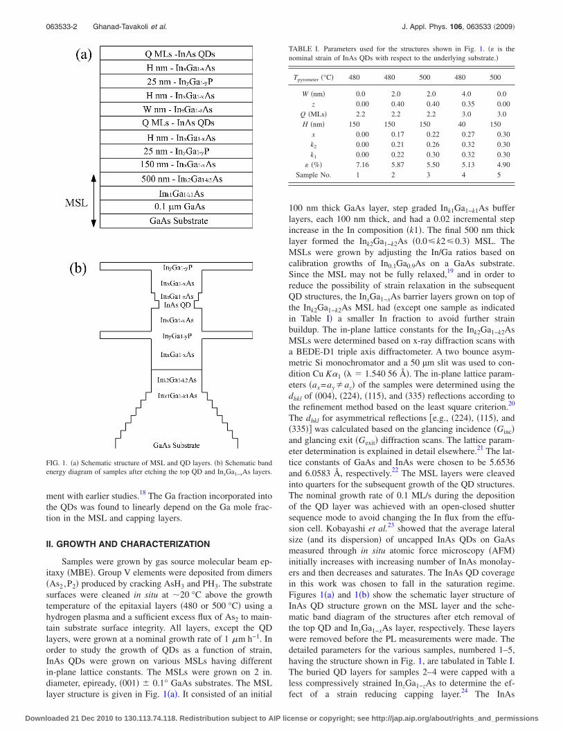
Samples were grown by gas source molecular beam ep-itaxy �MBE�. Group V elements were deposited from dimers�As2,P2� produced by cracking AsH3 and PH3. The substratesurfaces were cleaned in situ at �20 °C above the growthtemperature of the epitaxial layers �480 or 500 °C� using ahydrogen plasma and a sufficient excess flux of As2 to main-tain substrate surface integrity. All layers, except the QDlayers, were grown at a nominal growth rate of 1 �m h−1. Inorder to study the growth of QDs as a function of strain,InAs QDs were grown on various MSLs having differentin-plane lattice constants. The MSLs were grown on 2 in.diameter, epiready, �001� � 0.1° GaAs substrates. The MSLlayer structure is given in Fig. 1�a�. It consisted of an initial
100 nm thick GaAs layer, step graded Ink1Ga1−k1As bufferlayers, each 100 nm thick, and had a 0.02 incremental stepincrease in the In composition �k1�. The final 500 nm thicklayer formed the Ink2Ga1−k2As �0.0�k2�0.3� MSL. TheMSLs were grown by adjusting the In/Ga ratios based oncalibration growths of In0.1Ga0.9As on a GaAs substrate.Since the MSL may not be fully relaxed,19 and in order toreduce the possibility of strain relaxation in the subsequentQD structures, the InxGa1−xAs barrier layers grown on top ofthe Ink2Ga1−k2As MSL had �except one sample as indicatedin Table I� a smaller In fraction to avoid further strainbuildup. The in-plane lattice constants for the Ink2Ga1−k2AsMSLs were determined based on x-ray diffraction scans witha BEDE-D1 triple axis diffractometer. A two bounce asym-metric Si monochromator and a 50 µm slit was used to con-dition Cu K�1 �� � 1.540 56 Å�. The in-plane lattice param-eters �ax=ay �az� of the samples were determined using thedhkl of �004�, �224�, �115�, and �335� reflections according tothe refinement method based on the least square criterion.20
The dhkl for asymmetrical reflections �e.g., �224�, �115�, and�335�� was calculated based on the glancing incidence �Ginc�and glancing exit �Gexit� diffraction scans. The lattice param-eter determination is explained in detail elsewhere.21 The lat-tice constants of GaAs and InAs were chosen to be 5.6536and 6.0583 Å, respectively.22 The MSL layers were cleavedinto quarters for the subsequent growth of the QD structures.The nominal growth rate of 0.1 ML/s during the depositionof the QD layer was achieved with an open-closed shuttersequence mode to avoid changing the In flux from the effu-sion cell. Kobayashi et al.23 showed that the average lateralsize �and its dispersion� of uncapped InAs QDs on GaAsmeasured through in situ atomic force microscopy �AFM�initially increases with increasing number of InAs monolay-ers and then decreases and saturates. The InAs QD coveragein this work was chosen to fall in the saturation regime.Figures 1�a� and 1�b� show the schematic layer structure ofInAs QD structure grown on the MSL layer and the sche-matic band diagram of the structures after etch removal ofthe top QD and InxGa1−xAs layer, respectively. These layerswere removed before the PL measurements were made. Thedetailed parameters for the various samples, numbered 1–5,having the structure shown in Fig. 1, are tabulated in Table I.The buried QD layers for samples 2–4 were capped with aless compressively strained InzGa1−zAs to determine the ef-fect of a strain reducing capping layer.24 The InAs
TABLE I. Parameters used for the structures shown in Fig. 1. �� is thenominal strain of InAs QDs with respect to the underlying substrate.�
Tpyrometer �°C� 480 480 500 480 500
W �nm� 0.0 2.0 2.0 4.0 0.0z 0.00 0.40 0.40 0.35 0.00
Q �MLs� 2.2 2.2 2.2 3.0 3.0H �nm� 150 150 150 40 150
x 0.00 0.17 0.22 0.27 0.30k2 0.00 0.21 0.26 0.32 0.30k1 0.00 0.22 0.30 0.32 0.30
� �%� 7.16 5.87 5.50 5.13 4.90Sample No. 1 2 3 4 5
FIG. 1. �a� Schematic structure of MSL and QD layers. �b� Schematic bandenergy diagram of samples after etching the top QD and InxGa1−xAs layers.
063533-2 Ghanad-Tavakoli et al. J. Appl. Phys. 106, 063533 �2009�
Downloaded 21 Dec 2010 to 130.113.74.118. Redistribution subject to AIP license or copyright; see http://jap.aip.org/about/rights_and_permissions
QD/InxGa1−xAs layers were sandwiched between twoInyGa1−yP barrier layers, grown lattice matched to the neigh-boring InxGa1−xAs layers, to confine carriers and enhance thePL emission. The nominal strains are calculated based on thelateral lattice parameter of the MSL, determined from x-raymeasurements, and the InAs lattice constant �assuming noGa and In interdiffusion between the QDs and adjacent bar-rier layers�. The structures were terminated with an InAs QDlayer for size distribution analysis by AFM and the sampleswere cooled under an As2 flux after completion of thegrowth.
AFM was used to analyze the surface QDs. AMultiMode® Digital Instruments scanning probe microscopewas employed in Tapping Mode™; a standard Si cantileverwas used with a tetrahedral tip manufactured by Olympus�OMCL-AC160TS�. The mean free distance between thebases of the dots based on plan view transmission electronmicroscopy �TEM� of sample 5 �not show here� is approxi-mately �1.6 times larger than the nominal size of the canti-lever tip. To extract lateral size distribution of the QDs, theAFM images were exported in black and white and thenprocessed with IMAGEJ software.25 The size of the imageswas calibrated based on the actual AFM scan area. The bor-
der of the QDs versus the background was set based on thecontrast in the grayscale image. The QD density was calcu-lated according to scan size and number of the QDs �QDs onthe edge of the images were counted half since they wereshared by the neighboring images�. The circularity ratio ofthe QDs was determined to be close to unity so the diameterwas correlated with the area of the QDs. The diameters werethen graphed to yield the lateral diameter size distribution.The graphs are based on the superposition of three differentscan areas. Height distributions were extracted from Nano-Scope Ver. 7.30 provided by Veeco Instruments, Inc. For thePL analysis of the buried QDs, the surface QDs were re-moved by etching in buffered HF for 30 s after a 20 minUV-ozone exposure. The top InxGa1−xAs layer was then se-lectively removed using 1 H2SO4: 8 H2O2: 80 H2O for 30 sprior to the PL measurements. The samples were excitedby an argon ion laser �� � 488 nm� and the emission spectrawere collected at room temperature with an ABB BommemMB-160 Fourier transform infrared spectrometer with anInGaAs detector.
III. EXPERIMENTAL RESULTS
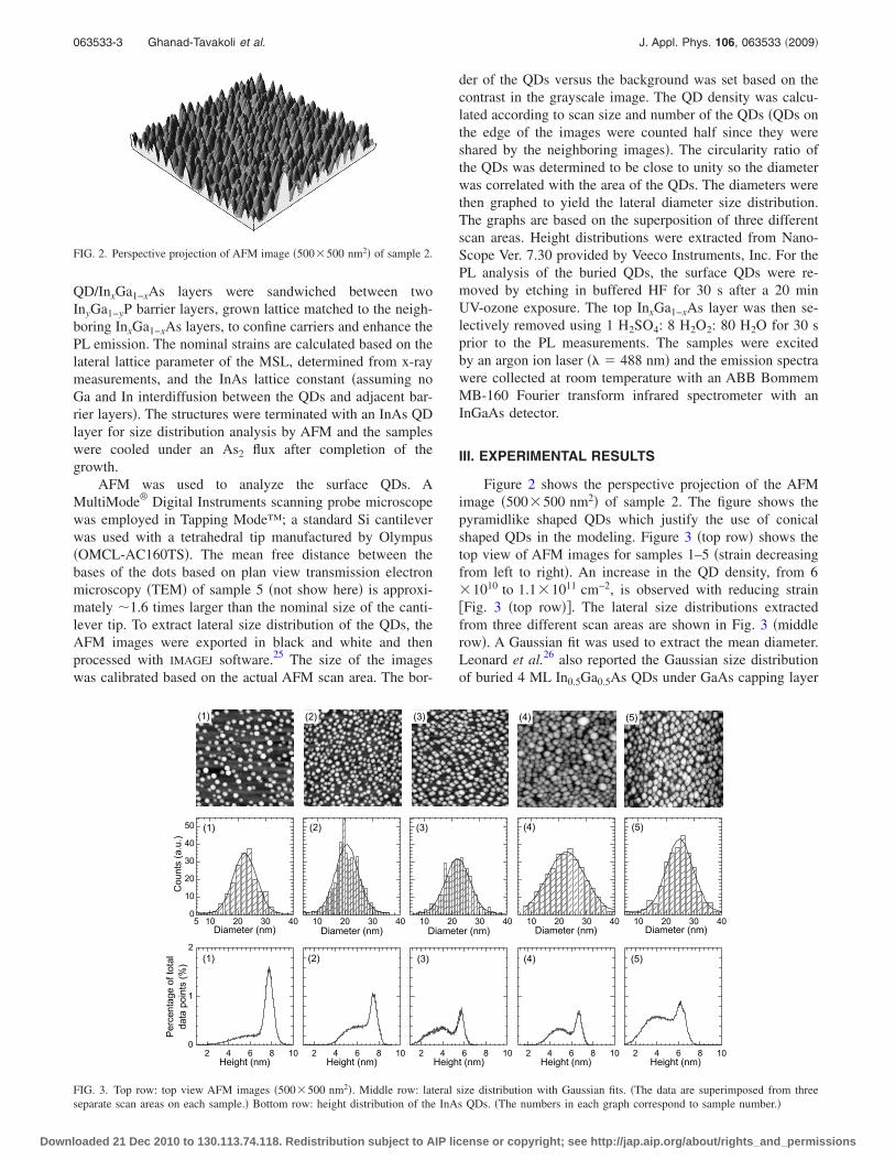
Figure 2 shows the perspective projection of the AFMimage �500�500 nm2� of sample 2. The figure shows thepyramidlike shaped QDs which justify the use of conicalshaped QDs in the modeling. Figure 3 �top row� shows thetop view of AFM images for samples 1–5 �strain decreasingfrom left to right�. An increase in the QD density, from 6�1010 to 1.1�1011 cm−2, is observed with reducing strain�Fig. 3 �top row��. The lateral size distributions extractedfrom three different scan areas are shown in Fig. 3 �middlerow�. A Gaussian fit was used to extract the mean diameter.Leonard et al.26 also reported the Gaussian size distributionof buried 4 ML In0.5Ga0.5As QDs under GaAs capping layer
FIG. 2. Perspective projection of AFM image �500�500 nm2� of sample 2.
FIG. 3. Top row: top view AFM images �500�500 nm2�. Middle row: lateral size distribution with Gaussian fits. �The data are superimposed from threeseparate scan areas on each sample.� Bottom row: height distribution of the InAs QDs. �The numbers in each graph correspond to sample number.�
063533-3 Ghanad-Tavakoli et al. J. Appl. Phys. 106, 063533 �2009�
Downloaded 21 Dec 2010 to 130.113.74.118. Redistribution subject to AIP license or copyright; see http://jap.aip.org/about/rights_and_permissions
on a GaAs substrate measured with plan view TEM. Theheight distributions of the QDs �Fig. 3 �bottom row�� reveala shoulder in the shorter tail of the profile, which can beexplained in agreement with previous reports27 that typicallytwo pyramidal- and dome-shaped families of faceted islandsexist �and/or coexist�. The diameter and height of sample 1are in agreement with previous reports28 of uncapped InAsislands on a GaAs substrate extracted from TEM or AFMmicrographs. It should be reiterated that although the abso-lute size of the QDs are overestimated in both TEM18,26 andAFM measurements, the distribution and their relative sizeswill remain unaffected.
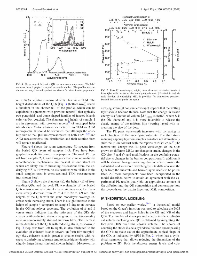
Figure 4 shows the room temperature PL spectra fromthe buried QD layers of samples 1–5. They have beengraphed in scale for comparison purposes. The weak PL sig-nal from samples 2, 4, and 5 suggests that some nonradiativerecombination mechanisms are present in our structureswhich are likely due to threading dislocations from the un-derlying MSLs. However, no dislocations were visible in thesmall samples used in cross-sectional TEM measurements�not shown here�.
Figure 5 shows the diameter �d�, the height �h� of free-standing QDs, and the peak PL wavelengths of the buriedQDs versus nominal strain. As the strain increases, the diam-eters slowly decrease from 25 � 4.9 to 22 � 4.9 nm. Theheights of the QDs with the same monolayer coverage in-crease with increasing strain. There is a slight increase in theheight of sample 4 compared to sample 3 due to an increasein the QD monolayer coverage. The evolution of d and hversus strain indicates that the ratio h /d of the QDs de-creases with reducing strain analogous to the tetragonalityratio in compressively strained uniform films. The increasein the densities of the QDs with reducing strain, as shown inFig. 3 �top row from left to right�, is also attributed to theevolution of coherent islands toward uniform film morphol-ogy �i.e., coherent islands grown at smaller strains with re-spect to underlying substrate tend to have higher density withslightly larger lateral size and shorter height�. Moreover, in-
creasing strain �at constant coverage� implies that the wettinglayer should become thinner. Note that the change in elasticenergy is a function of volume �Eelastic�c���D3, where D isthe QD diameter� and it is more favorable to release theelastic energy of the uniform film �wetting layer� with in-creasing the size of the dots.
The PL peak wavelength increases with increasing Inmole fraction of the underlying substrate. The thin strainreducing capping layer on samples 2–4 does not dramaticallyshift the PL in contrast with the reports of Nishi et al.24 Thefactors that change the PL peak wavelength of the QDsgrown on different MSLs are change in strain, changes in theQD size �h and d�, and modifications in the confining poten-tial due to changes in the barrier compositions. In addition, itwill be shown, through modeling, that in order to match thecalculated and measured wavelengths, Ga diffusion into theQDs from the substrate and barrier layers needs to be postu-lated. All these components have been incorporated in themodel described below to obtain an agreement with the ex-perimental PL results that yield an approximate amount ofGa diffusion into the QD composition and demonstrate howthis depends on the barrier layer and MSL composition.
IV. THEORETICAL MODELING
Based on our earlier works,29–31 a theoretical modelbased on the Green’s function was used to calculate the DOSof the electrons and heavy holes in the CB and VB of theQDs. The number of states per unit energy inside a cylindri-cal volume enclosing one QD is obtained by integrating thelocalized DOS over this chosen volume. The choice ofcounting the states inside a cylindrical volume encompassingthe QD is to make use of the approximate conical shape ofthe QD, as indicated by AFM in Fig. 2, which has a cylin-drical symmetry that allows reducing the dimensions of theproblem to 2D. Both the discrete energy levels and con-
FIG. 4. PL spectra of the buried QD layers at room temperature. The labelnumbers in each graph correspond to sample number. �The profiles are con-tinuous and only selected symbols are shown for identification purposes.� FIG. 5. Peak PL wavelength, height, mean diameter vs nominal strain of
InAs QDs with respect to the underlying substrate. �Nominal In and Gamole fraction of underlying MSL is provided for comparison purposes.Dashed lines are to guide the eyes.�
063533-4 Ghanad-Tavakoli et al. J. Appl. Phys. 106, 063533 �2009�
Downloaded 21 Dec 2010 to 130.113.74.118. Redistribution subject to AIP license or copyright; see http://jap.aip.org/about/rights_and_permissions

tinuum part of the spectrum for the QD inside the cylindercan be obtained. To obtain the Hamiltonian of the QD insidethe cylinder, the CB and VB offset variations, the effectivemasses for the QD, the surrounding substrate, and the barriermaterials need to be obtained. The different MSLs will givedifferent applied strains, which lead to variations in the QDband gap and band offsets; hence, the confining barrier po-tential. The Hamiltonian obtained for the QD should includethe effect of coupling with the surroundings outside the cyl-inder through the inclusion of the self-energy. After obtain-ing the total Hamiltonian of the QD including the couplingself-energy, the kinetic equation of the Green’s function issolved numerically using the method of finite differences.The localized DOS is obtained from the Green’s function,which is integrated over the cylindrical volume to get theDOS of the QD.30 A schematic of the InAs QD structure,based on the samples measured, is shown in Fig. 6. The QDsare grown on an InxGa1−xAs substrate and capped with thesame material. In some samples, a thin strain relieving layerwas grown before the spacer layer of the substrate materialbut this was found to have no significant effect on the peakPL wavelength so these structures will not be modeled. Theschematic of the model used in the calculation of the DOS ofthe QD is shown in Fig. 6�a�, which is drawn in the r-z planepassing through the axis of the conical shape QD.
Figure 6�b� shows a schematic of the grid used for thenumerical solution. The band offset potential energies andeffective masses are obtained at every point in the grid. Thegrid spacing is chosen to be 0.25 nm. The self-energies,which represent the coupling with the surroundings, areadded at the interfacial points of the cylinder. The averageheight and diameter for different samples are extracted fromthe fitting lines that show the dependence of the averageheight and diameter of the QDs on the underlying strain. Ithas previously been established18,28,32 that the average heightof surface QDs obtained by AFM is reduced during the cap-ping growth; hence, we considered a reduction by a factor of12 in the height of the QDs obtained from AFM measurementin agreement with previous experimental reports.18,28 Also,the wetting layer thickness is expected to depend on theamount of strain, but for simplicity, it will be assumed con-
stant in the model and its value is taken to be 0.5 nm. Theradius and height of the cylinder surrounding the QD arechosen to enclose only one QD and are chosen to be 20 and30 nm, respectively.
A. Band gap and band offset calculations
The band gap of unstrained InxGa1−xAs can be calculatedfrom the simple quadratic formula33
Eg�InxGa1−xAs� = xEg�InAs� + �1 − x�Eg�GaAs�
− x�1 − x�C , �1�
where C is called the bowing parameter to account for thedeviation from the linear interpolation and is 477 meV forInxGa1−xAs.33 The effective masses for both electron andheavy hole have a similar quadratic relation and the bowingparameters are 0.0091 and 0.145 for electron and hole,respectively.33 The band gap of InAs and GaAs at room tem-peratures are 354 and 1424 meV, respectively.33 The effec-tive masses for electron and hole for InAs are 0.023 and 0.4,respectively, while for GaAs are 0.067 and 0.5,respectively.33 The CB and VB offsets of InAs compared toGaAs are taken to be 60% and 40% of the band gap differ-ence, respectively.34,35 For the InxGa1−xAs substrate, thesame band offset ratios will be assumed to be the same as inthe case of GaAs.
The band gap of the QD calculated from Eq. �1� is thenmodified to include the effect of strain. First, InAs QDs willbe considered in the calculations. It was found that a goodagreement with the PL data could not be obtained. However,it has been shown18 that Ga outdiffusion from the barrierlayers into the QD occurs during growth; thus, Ga incorpo-ration was considered in the model as a fitting parameter tofine tune the results of the model compared to the measuredPL peak. The unstrained values of the band gap for the QDand the surrounding barriers will be calculated using Eq. �1�.
The lattice constant of InxGa1−xAs is given by the fol-lowing linear relation:
aInxGa1−xAs = a�x� = xaInAs + �1 − x�aGaAs. �2�
The lateral or the in-plane strain36 for the InAs QDgrown on InxGa1−xAs is given by
� = �xx = �yy =a�x� − aInAs
a�x�. �3�
While the strain in the perpendicular direction is givenby
�� = �zz = − 2�
1 − �� = − 2
C12
C11� , �4�
where � is Poisson’s ratio and C12 and C11 are the elasticstiffness constants of the strained QD material. Following theanalysis given in Ref. 36, the effective band gap for strainedInxGa1−xAs, conduction to heavy hole band gap, is given bythe relation
FIG. 6. �Color online� �a� Schematic of a cylindrical volume containingInAs QD surrounded by InxGa1−xAs barrier used for formulating the poten-tial and effective mass distributions. �b� Schematic of the lattice grid in ther-z plane used in the numerical simulation. The surrounding contact layersare replaced by self-energies at the interface place of the QD cylinder.
063533-5 Ghanad-Tavakoli et al. J. Appl. Phys. 106, 063533 �2009�
Downloaded 21 Dec 2010 to 130.113.74.118. Redistribution subject to AIP license or copyright; see http://jap.aip.org/about/rights_and_permissions
EC–HH = Eg�x� + 2a�1 −C12
C11�� − b�1 + 2
C12
C11�� , �5�
where Eg�x� is the unstrained band gap and is given by Eq.�1�, a is defined as the hydrostatic deformation potential, anda and b are constants and tabulated for different III/V semi-conductor materials. The constants for a, b, C12, and C11 areused as given in Ref. 36 for InAs and GaAs, and forInxGa1−xAs, a linear interpolation is used to extract theseparameters.
B. Green’s function model
The retarded Green’s function of the QD inside the cyl-inder in cylindrical coordinate matrix form and energy rep-resentation is given by29,37
�EI − H − �r�Gr = �r�−1, �6�
where E is the total energy of electrons or holes, H is thediscretized matrix representation of the Hamiltonian opera-tor, �r is the self-energy due to coupling with the surround-ings, and �r� is a diagonal matrix whose diagonal elementsare the radial part of the position vector. The Hamiltonianoperator Hop in the cylindrical coordinate is given by
Hop = − 2
2�1
r
�
�r
r
mr�r,z��
�r+
1
mr�r,z�1
r2
�2
��2
+�
�z
1
mz�r,z��
�z + V�r,z� , �7�
where V�r ,z� is the potential energy which is the CB or VBoffset variations for the QD and substrate materials. The di-agonal elements of the localized DOS is related to theGreen’s function by the relation37
A�r,z;E� = − 2 Im�Gr�r,r;�,�;z,z;E�� . �8�
The DOS, which is the number of states per unit energyinside the cylinder, is obtained from the trace of the localizedDOS over the cylindrical volume and is given by
D�E� =1
2�Tr�A�r,z;E�� =
1
2� 2�rdrdzA�r,z;E� . �9�
The model has been discussed in detail in Ref. 30.
C. Simulation results
The Green’s function is calculated numerically from Eq.�6� by doing a matrix inversion at certain values of E and n.The QD density based on AFM measurements is�1011 cm−2, so the average separation of QDs is �20 nm.The height and radius of the cylinder to enclose one QD arechosen to be 30 and 20 nm, respectively. The grid step is0.25 nm; hence, the schematic shown in Fig. 6�b� contains 80and 120 lattice points in r and z dimensions, respectively,and the Hamiltonian matrix dimension is 9600 � 9600. Thelocalized DOS is calculated from the Green’s function fromEq. �8�. For the energy ranges used in the calculations, thefirst six terms in the series are enough to produce the re-quired DOS for both the discrete and continuum parts of thespectrum near the top of the potential barrier surrounding the
QDs. The contributions to the DOS from the terms corre-sponding to negative values of n are equal the ones corre-sponding to the positive values due to the Hamiltonian de-generacy with respect to n. Therefore, there is no need forfurther calculations of the negative terms and instead theterms corresponding to positive values of n are multiplied by2.
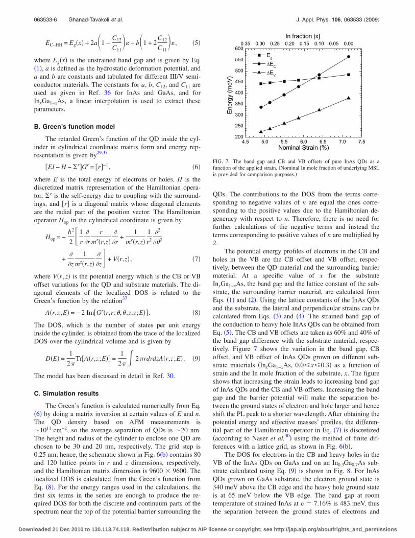
The potential energy profiles of electrons in the CB andholes in the VB are the CB offset and VB offset, respec-tively, between the QD material and the surrounding barriermaterial. At a specific value of x for the substrateInxGa1−xAs, the band gap and the lattice constant of the sub-strate, the surrounding barrier material, are calculated fromEqs. �1� and �2�. Using the lattice constants of the InAs QDsand the substrate, the lateral and perpendicular strains can becalculated from Eqs. �3� and �4�. The strained band gap ofthe conduction to heavy hole InAs QDs can be obtained fromEq. �5�. The CB and VB offsets are taken as 60% and 40% ofthe band gap difference with the substrate material, respec-tively. Figure 7 shows the variation in the band gap, CBoffset, and VB offset of InAs QDs grown on different sub-strate materials �InxGa1−xAs, 0.0�x�0.3� as a function ofstrain and the In mole fraction of the substrate, x. The figureshows that increasing the strain leads to increasing band gapof InAs QDs and the CB and VB offsets. Increasing the bandgap and the barrier potential will make the separation be-tween the ground states of electron and hole larger and henceshift the PL peak to a shorter wavelength. After obtaining thepotential energy and effective masses’ profiles, the differen-tial part of the Hamiltonian operator in Eq. �7� is discretized�according to Naser et al.30� using the method of finite dif-ferences with a lattice grid, as shown in Fig. 6�b�.
The DOS for electrons in the CB and heavy holes in theVB of the InAs QDs on GaAs and on an In0.3Ga0.7As sub-strate calculated using Eq. �9� is shown in Fig. 8. For InAsQDs grown on GaAs substrate, the electron ground state is340 meV above the CB edge and the heavy hole ground stateis at 65 meV below the VB edge. The band gap at roomtemperature of strained InAs at � � 7.16% is 483 meV, thusthe separation between the ground states of electrons and
FIG. 7. The band gap and CB and VB offsets of pure InAs QDs as afunction of the applied strain. �Nominal In mole fraction of underlying MSLis provided for comparison purposes.�
063533-6 Ghanad-Tavakoli et al. J. Appl. Phys. 106, 063533 �2009�
Downloaded 21 Dec 2010 to 130.113.74.118. Redistribution subject to AIP license or copyright; see http://jap.aip.org/about/rights_and_permissions

heavy holes is 888 meV, corresponding to � � 1396 nm. ForInAs grown on an In0.3Ga0.7As substrate, the ground stateenergy levels of the electrons and holes shift to lower energylevels compared to the CB and VB edges and the higherexcited states of the electrons are no longer confined. Thisshift of the ground states and disappearance of the excitedstates are due to the lower barrier potential confinements�i.e., the CB and VB offsets decrease�. The band gap ofstrained InAs at � � 4.9% is 442 meV and the energy tran-sition between the ground states of electrons and holes andthe corresponding wavelength are 778 meV and 1592 nm.
The results obtained by the model for the PL peak wave-length are compared to the available experimental results inFig. 9. The experimental results can be fitted by a straightline that shows the linear increase in the PL peak wavelengthwith increasing In mole fraction in the substrate. There is a
qualitative agreement between the model and the experimen-tal results concerning the increase in the PL wavelength withdecreasing strain �increasing In mole fraction of the MSL�;however, the model yields longer wavelengths presumablybecause pure InAs QDs are assumed. In practice, it has beenshown that Ga outdiffusion from the substrate and barrierlayers occurs during the growth.18,28 Diffusion of Ga into theQDs will modify the lattice constant, effective masses, bandgap, CB, and VB offsets. The increase in the band gap blue-shifts the modeling results, while the decrease in the bandoffsets redshifts the results. Also, the strain decreases due tothe decrease in the lattice constant; the strain effect on theband gap will be less and the band gap increases due to Gaaddition. By adjusting the model to include Ga in the QDs, itis possible to fit the experimental data and determine theamount of Ga incorporated as a function of the Ga molefraction contained in the InxGa1−xAs MSL and barrier.
FIG. 8. The DOS of electrons in the CB and heavy holes in the VB for InAs QDs grown on InxGa1−xAs substrates at x=0.0 and 0.3.
FIG. 9. Comparison between the experimental and the calculated PL peakwavelength at different nominal strains. �Nominal In mole fraction of un-derlying MSL is provided for comparison purposes.�
FIG. 10. Comparison between the modeling and experimental results con-cerning the PL peak wavelength at different adjusted strains. InqGa1−qAsQDs are used in the simulation, where q=0.33x+0.80.
063533-7 Ghanad-Tavakoli et al. J. Appl. Phys. 106, 063533 �2009�
Downloaded 21 Dec 2010 to 130.113.74.118. Redistribution subject to AIP license or copyright; see http://jap.aip.org/about/rights_and_permissions
Figure 10 shows the fit between the experimental resultsand the model considering InqGa1−qAs QDs grown onInxGa1−xAs MSL. It was found that the model and experi-mental results agree when q=0.33x+0.80 for 0.0�x�0.3.
Incorporation of Ga into the InAs QDs modifies the lat-tice constant, effective masses, band gap, and CB and VBoffsets. The strain decreases due to the decrease in the latticeconstant with the Ga intermixing into the InAs QDs; thus,the effect of the strain on the band gap will become less.Moreover, the band gap increases due to the Ga addition. Onthe other hand, the CB and VB offsets will decrease as theQD band gap increases relative to the surrounding barriers.The increase in the band gap blueshifts the results, while thedecrease in the band offsets redshifts them. However, theincrease in the band gap is larger than the reduction in theground states due to the decrease in potential barriers. Notethat the Ga incorporation becomes larger, and hence the in-terband transition blueshifts more with increasing Ga molefraction of the MSL.
V. CONCLUSIONS
The strain effect on the size distribution and opticalproperties of InAs QDs grown on InxGa1−xAs �0.0�x�0.3� MSLs has been studied experimentally. The ratio ofthe height �h�/lateral diameter �D� of the QDs decreases withdecreasing strain. The evolution is analogous to the currentunderstating of strained uniform films where the tetragonal-ity of a uniform film increases with increasing strain. As theIn mole fraction in the metamorphic substrate is increased,the measured PL peak wavelength increases. A theoreticalmodel based on Green’s function is used to calculate theDOS for both electrons and holes in the CB and VB, respec-tively. The model assigns the increase in the wavelength ofthe PL to the decrease in the QD band gap and also to thedecrease in the CB and VB offsets confining potentials.Good agreement between the theoretical model and the ex-perimental results is obtained when the QD composition isadjusted to contain Ga in direct proportion to the Ga molefraction contained in the substrate.
ACKNOWLEDGMENTS
S.G.-T. thanks Dr. Robinson for MBE growth. This workwas supported in part by grants from the Natural Sciencesand Engineering Research Council �NSERC� of Canada, theCanada Research Chair �CRC� program, and by Ontario Pho-tonics Consortium �Photonics Research Ontario�.
1D. L. Huffaker, G. Park, Z. Zou, O. B. Shchekin, and D. G. Deppe, Appl.Phys. Lett. 73, 2564 �1998�.
2L. F. Lester, A. Stintz, H. Li, T. C. Newell, E. A. Pease, B. A. Fuchs, andK. J. Malloy, IEEE Photonics Technol. Lett. 11, 931 �1999�.
3A. E. Zhukov, A. R. Kovsh, N. A. Maleev, S. S. Mikhrin, V. M. Ustinov,A. F. Tsatsul’nikov, M. V. Maximov, B. V. Volovik, D. A. Bedarev, Yu. M.Shernyakov, P. S. Kop’ev, Zh. I. Alferov, N. N. Ledentsov, and D. Bim-berg, Appl. Phys. Lett. 75, 1926 �1999�.
4A. E. Zhukov, A. R. Kovsh, V. M. Ustinov, Yu. M. Shernyakov, S. S.Mikhrin, N. A. Maleev, E. Yu. Kondrat’eva, D. A. Livshits, M. V. Maxi-mov, B. V. Volovik, D. A. Bedarev, Yu. G. Musikhin, N. N. Ledentsov,P.S. Kop’ev, Z. I. Alferov, and D. Bimberg, IEEE Photonics Technol. Lett.11, 1345 �1999�.
5Y. Nakata, K. Mukai, M. Sugawara, K. Ohtsubo, H. Ishikawa, and N.
Yokoyama, J. Cryst. Growth 208, 93 �2000�.6L. Ya. Karachinsky, T. Kettler, I. I. Novikov, Yu. M. Shernyakov, N. Yu.Gordeev, M. V. Maximov, N. V. Kryzhanovskaya, A. E. Zhukov, E. S.Semenova, A. P. Vasil’ev, V. M. Ustinov, G. Fiol, M. Kuntz, A. Loch-mann, O. Schulz, L. Reissmann, K. Posilovic, A. R. Kovsh, S. S. Mikhrin,V. A. Shchukin, N. N. Ledentsov, and D. Bimberg, Semicond. Sci. Tech-nol. 21, 691 �2006�.
7N. N. Ledentsov, A. R. Kovsh, A. E. Zhukov, N. A. Maleev, S. S.Mikhrin, A. P. Vasil’ev, E. S. Semenova, M. V. Maximov, Yu. M.Shernyakov, N. V. Kryzhanovskaya, V. M. Ustinov, and D. Bimberg, Elec-tron. Lett. 39, 1126 �2003�.
8S. Haffouz, S. Raymond, Z. G. Lu, P. J. Barrios, D. Roy-Guay, X. Wu, J.R. Liu, D. Poitras, and Z. R. Wasilewski, J. Cryst. Growth 311, 1803�2009�.
9M. Asada, Y. Miyamoto, and Y. Suematsu, IEEE J. Quantum Electron. 22,1915 �1986�.
10R. P. Mirin, J. P. Ibbetson, K. Nishi, A. C. Gossard, and J. E. Bowers,Appl. Phys. Lett. 67, 3795 �1995�.
11H. Saito, K. Nishi, and Sh. Sugou, Appl. Phys. Lett. 73, 2742 �1998�.12E. C. Le Ru, A. J. Bennett, C. Roberts, and R. Murray, J. Appl. Phys. 91,
1365 �2002�.13M. Grundmann, N. N. Ledentsov, F. Hopfer, F. Heinrichsdorff, F. Guf-
farth, D. Bimberg, V. M. Ustinov, A. E. Zhukov, A. R. Kovsh, M. V.Maximov, Yu. G. Musikhin, Zh. I. Alferov, J. A. Lott, N. D. Zhakharov,and P. Werner, J. Mater. Sci.: Mater. Electron. 13, 643 �2002�.
14V. M. Ustinov, A. E. Zhukov, A. R. Kovsh, S. S. Mikhrin, N. A. Maleev,B. V. Volovik, Yu. G. Musikhin, Yu. M. Shernyakov, E. Yu. Kondat’eva,M. V. Maximov, A. F. Tsatsul’nikov, N. M. Ledentsov, Zh. I. Alferov, J.A. Lott, and D. Bimberg, Nanotechnology 11, 397 �2000�.
15A. Zhukov, A. Vasilyev, E. Semenova, N. Kryzhanovskaya, A. Gladyshev,M. Maximov, V. Ustinov, and N. Ledentsov, Proc. SPIE 5946, 594616�2005�.
16L. Seravalli, M. Minelli, P. Frigeri, P. Allegri, V. Avanzini, and S. Franchi,Appl. Phys. Lett. 82, 2341 �2003�.
17N. N. Ledentsov, A. R. Kovsh, V. A. Shchukin, S. S. Mikhrin, I. L.Krestnikov, and A. V. Kozhukhov, Proc. SPIE 5624, 335 �2005�.
18P. D. Siverns, S. Malik, G. McPherson, D. Childs, C. Roberts, R. Murray,B. A. Joyce, and H. Davock, Phys. Rev. B 58, R10127 �1998�.
19J. Tersoff, Appl. Phys. Lett. 62, 693 �1993�.20M. Fatemi, J. Cryst. Growth 207, 188 �1999�.21S. G. Tavakoli, O. Hulko, and D. A. Thompson, J. Appl. Phys. 103,
103527 �2008�.22O. Madelung, Semiconductors: Data Handbook, 3rd ed. �Springer, Berlin,
2004�.23N. P. Kobayashi, T. R. Ramachandran, P. Chen, and A. Madhukar, Appl.
Phys. Lett. 68, 3299 �1996�.24K. Nishi, H. Saito, Sh. Sugou, and J.-S. Lee, Appl. Phys. Lett. 74, 1111
�1999�.25M. D. Abramoff, P. J. Magelhaes, and S. J. Ram, Biophotonics Int. 11, 36
�2004�.26D. Leonard, M. Krishnamurthy, C. M. Reaves, S. P. Denbaars, and P. M.
Petroff, Appl. Phys. Lett. 63, 3203 �1993�.27G. Costantini, A. Rastelli, C. Manzano, R. Songmuang, O. G. Schmidt, K.
Kern, and H. v. Kanel, Appl. Phys. Lett. 85, 5673 �2004�.28D. Leonard, M. Krishnamurthy, S. Fafard, J. L. Merz, and P. M. Petroff, J.
Vac. Sci. Technol. B 12, 1063 �1994�.29M. A. Naser, M. J. Deen, and D. A. Thompson, J. Appl. Phys. 102,
083108 �2007�.30M. A. Naser, M. J. Deen, and D. A. Thompson, J. Appl. Phys. 100,
093102 �2006�.31M. A. Naser, M. J. Deen, and D. A. Thompson, J. Appl. Phys. 104, 014511
�2008�.32J. M. Garcia, G. Medeiros-Ribeiro, K. Schmidt, T. Ngo, J. L. Feng, A.
Lorke, J. Kotthaus, and P. M. Petroff, Appl. Phys. Lett. 71, 2014 �1997�.33I. Vurgaftman, J. R. Meyer, and L. R. Ram-Mohan, J. Appl. Phys. 89,
5815 �2001�.34S. Chakrabarti, A. D. Stiff-Robert, P. Battacharya, and S. W. Kennerly,
Electron. Lett. 40, 197 �2004�.35A. D. Stiff, S. Krishna, P. Bhattacharya, and S. Kennerly, IEEE J. Quan-
tum Electron. 37, 1412 �2001�.36S. L. Chuang, Physics of Optoelectronic Devices �Wiley, New York,
1995�.37S. Datta, Electronic Transport in Mesoscopic Systems �Cambridge Univer-
sity Press, Cambridge, UK, 1995�.
063533-8 Ghanad-Tavakoli et al. J. Appl. Phys. 106, 063533 �2009�
Downloaded 21 Dec 2010 to 130.113.74.118. Redistribution subject to AIP license or copyright; see http://jap.aip.org/about/rights_and_permissions