
Evidence for anisotropic dielectric properties of monoclinic hafnia using valence electron...
6
Evidence for anisotropic dielectric properties of monoclinic hafnia using valence electron energy-loss spectroscopy in high-resolution transmission electron microscopy and ab initio time-dependent density-functional theory C. Guedj, L. Hung, A. Zobelli, P. Blaise, F. Sottile, and V. Olevano Citation: Applied Physics Letters 105, 222904 (2014); doi: 10.1063/1.4903218 View online: http://dx.doi.org/10.1063/1.4903218 View Table of Contents: http://scitation.aip.org/content/aip/journal/apl/105/22?ver=pdfcov Published by the AIP Publishing Articles you may be interested in Valence and ionic lowest-lying electronic states of ethyl formate as studied by high-resolution vacuum ultraviolet photoabsorption, He(I) photoelectron spectroscopy, and ab initio calculations J. Chem. Phys. 141, 104311 (2014); 10.1063/1.4894762 Direct visualization and characterization of chemical bonding and phase composition of grain boundaries in polycrystalline diamond films by transmission electron microscopy and high resolution electron energy loss spectroscopy Appl. Phys. Lett. 99, 201907 (2011); 10.1063/1.3660582 Calculated and experimental electron energy-loss spectra of La 2 O 3 , La ( OH ) 3 , and LaOF nanophases in high permittivity lanthanum-based oxide layers Appl. Phys. Lett. 98, 243116 (2011); 10.1063/1.3600783 Ab initio Real Space Calculations of Electron Energy Loss Spectra AIP Conf. Proc. 999, 47 (2008); 10.1063/1.2918116 Transformation of nanodiamond into carbon onions: A comparative study by high-resolution transmission electron microscopy, electron energy-loss spectroscopy, x-ray diffraction, small-angle x-ray scattering, and ultraviolet Raman spectroscopy J. Appl. Phys. 97, 074302 (2005); 10.1063/1.1868054 This article is copyrighted as indicated in the article. Reuse of AIP content is subject to the terms at: http://scitation.aip.org/termsconditions. Downloaded to IP: 129.104.29.2 On: Fri, 28 Aug 2015 14:44:49
-
Upload
polytechnique -
Category
Documents
-
view
1 -
download
0
Transcript of Evidence for anisotropic dielectric properties of monoclinic hafnia using valence electron...
Evidence for anisotropic dielectric properties of monoclinic hafnia using valenceelectron energy-loss spectroscopy in high-resolution transmission electronmicroscopy and ab initio time-dependent density-functional theoryC. Guedj, L. Hung, A. Zobelli, P. Blaise, F. Sottile, and V. Olevano Citation: Applied Physics Letters 105, 222904 (2014); doi: 10.1063/1.4903218 View online: http://dx.doi.org/10.1063/1.4903218 View Table of Contents: http://scitation.aip.org/content/aip/journal/apl/105/22?ver=pdfcov Published by the AIP Publishing Articles you may be interested in Valence and ionic lowest-lying electronic states of ethyl formate as studied by high-resolution vacuum ultravioletphotoabsorption, He(I) photoelectron spectroscopy, and ab initio calculations J. Chem. Phys. 141, 104311 (2014); 10.1063/1.4894762 Direct visualization and characterization of chemical bonding and phase composition of grain boundaries inpolycrystalline diamond films by transmission electron microscopy and high resolution electron energy lossspectroscopy Appl. Phys. Lett. 99, 201907 (2011); 10.1063/1.3660582 Calculated and experimental electron energy-loss spectra of La 2 O 3 , La ( OH ) 3 , and LaOF nanophases inhigh permittivity lanthanum-based oxide layers Appl. Phys. Lett. 98, 243116 (2011); 10.1063/1.3600783 Ab initio Real Space Calculations of Electron Energy Loss Spectra AIP Conf. Proc. 999, 47 (2008); 10.1063/1.2918116 Transformation of nanodiamond into carbon onions: A comparative study by high-resolution transmissionelectron microscopy, electron energy-loss spectroscopy, x-ray diffraction, small-angle x-ray scattering, andultraviolet Raman spectroscopy J. Appl. Phys. 97, 074302 (2005); 10.1063/1.1868054
This article is copyrighted as indicated in the article. Reuse of AIP content is subject to the terms at: http://scitation.aip.org/termsconditions. Downloaded to IP: 129.104.29.2
On: Fri, 28 Aug 2015 14:44:49

Evidence for anisotropic dielectric properties of monoclinic hafnia usingvalence electron energy-loss spectroscopy in high-resolution transmissionelectron microscopy and ab initio time-dependent density-functional theory
C. Guedj,1,2 L. Hung,3,4 A. Zobelli,5 P. Blaise,1,2,4 F. Sottile,3,4 and V. Olevano1,4,6
1University Grenoble Alpes, F-38000 Grenoble, France2CEA, LETI, MINATEC Campus, F-38054 Grenoble, France3LSI, CNRS, CEA, �Ecole Polytechnique, F-91128 Palaiseau, France4European Theoretical Spectroscopy Facility (ETSF)5LPS, CNRS and University Paris Sud, F-91405 Orsay, France6CNRS, Institut N�eel, F-38042 Grenoble, France
(Received 12 September 2014; accepted 7 November 2014; published online 2 December 2014)
The effect of nanocrystal orientation on the energy loss spectra of monoclinic hafnia (m-HfO2) is
measured by high resolution transmission electron microscopy (HRTEM) and valence energy loss
spectroscopy (VEELS) on high quality samples. For the same momentum-transfer directions, the
dielectric properties are also calculated ab initio by time-dependent density-functional theory
(TDDFT). Experiments and simulations evidence anisotropy in the dielectric properties of m-HfO2,
most notably with the direction-dependent oscillator strength of the main bulk plasmon. The aniso-
tropic nature of m-HfO2 may contribute to the differences among VEELS spectra reported in litera-
ture. The good agreement between the complex dielectric permittivity extracted from VEELS with
nanometer spatial resolution, TDDFT modeling, and past literature demonstrates that the present
HRTEM-VEELS device-oriented methodology is a possible solution to the difficult nanocharacteri-
zation challenges given in the International Technology Roadmap for Semiconductors. VC 2014AIP Publishing LLC. [http://dx.doi.org/10.1063/1.4903218]
With the downscaling of microelectronic and optoelec-
tronic devices, accurate metrology at the nanoscale has
become an important objective for the microelectronic indus-
try. At the same time, the International Technology
Roadmap for Semiconductors categorizes the “measurement
of complex material stacks and interface properties, includ-
ing physical and electrical properties” as a “difficult
challenge” for �16 nm CMOS technology nodes. The char-
acterization of high-j gate stacks (mostly based on hafnia-
based dielectrics) is particularly complicated due to the
length scales at which electronic properties are determined.
These new challenges for characterization and metrology
arise not only from the introduction of thinner and more
complex materials and stacks but also from the need to dis-
cern physical properties at an increasing spatial resolution.
To develop nanocharacterization protocols that are inde-
pendent of materials stacks and integration design, even
more advanced methods are required. Valence electron
energy-loss spectroscopy (VEELS) is the only technique ca-
pable of measuring dielectric and optical properties1 (com-
plex refractive index), and chemical properties2
(composition, atomic bonding) at the same time and with
nanometer spatial resolution, when all effects are properly
taken into account.3,4
In this paper, we use the energy filtered TEM-VEELS
technique (also known as EFTEM SI),8 in a high-resolution
transmission electron microscope (HRTEM) to simultane-
ously obtain the structural and spectroscopic properties of
P21/c m-HfO2 with nanometric spatial resolution. HfO2 is a
prominent high-j material used in various applications like
MIM capacitors,5 resistive memories (OxRRAM),6 or optical
coatings.7 To this purpose, the dielectric properties of
m-HfO2 corresponding to the different crystal configuration
and orientations that can be grown in an electronic device
must be precisely measured, a task for which HRTEM-
VEELS is particularly suited. After detailed nanostructural
modeling of HRTEM measurements using quantitative
image simulations, we obtained VEELS spectra for various
well identified m-HfO2 crystal orientations. For the same
momentum-transfer directions, we also calculate ab initiotime-dependent density-functional theory (TDDFT)11
energy-loss spectra. For the calculated TDDFT spectra, we
use the random-phase approximation (RPA) and also include
local-field effects.13,14 This level of theory allows us to
reproduce, interpret, and even predict experimental energy-
loss spectra.15 With its reliability and predictivity, TDDFT is
a valuable complement to experimentally applied research
on high-j materials for electronic or optical devices.
For the dielectric properties and spectra of m-HfO2, we
find a significant dependence on the crystal direction. The
analysis of the main oscillators of the EELS spectra shows
that the change in lattice orientation mostly affects the
strength of the main bulk plasmon excitation at �16 eV. A
significant anisotropy of �10% has been found also on the
dielectric constant.
HfO2 films are grown by atomic layer deposition (ALD)
on 200 mm p-Si(100) wafers. Before deposition, substrates
are treated with a diluted HF solution to remove any native
oxides. ALD takes place in an ASM Pulsar 2000TM module
at 350 �C using alternating pulses of HfCl4 and H2O, with N2
as a carrier gas. The introduction of H2O vapor is used to
desorb HCl at the growing surface, and the cycles are
repeated sequentially to reach a thickness sufficient to maxi-
mize the crystal quality and to minimize the surface losses.
0003-6951/2014/105(22)/222904/5/$30.00 VC 2014 AIP Publishing LLC105, 222904-1
APPLIED PHYSICS LETTERS 105, 222904 (2014)
This article is copyrighted as indicated in the article. Reuse of AIP content is subject to the terms at: http://scitation.aip.org/termsconditions. Downloaded to IP: 129.104.29.2
On: Fri, 28 Aug 2015 14:44:49
A final annealing at 650 �C is performed to crystallize HfO2
and minimize the amount of oxygen vacancies. A high Tauc-
Lorentz18,19 band gap (�5.9) is measured by spectroscopic
ellipsometry and VEELS, which is consistent20 with a low
level of oxygen vacancies of this fully oxidized HfO2 layer.
This layer is therefore representative of a good quality
dielectric material used in the microelectronic industry.
Additional measurements are performed on high grade m-
HfO2 powders for verification.
Cross-sectional electron microscopy and diffraction
experiments are performed in a JEOL 2010 FEF transmission
electron microscope (TEM) operated at 200 kV at a magnifi-
cation of 800 k, with an energy step of 0.1 eV between each
image acquisition. The lowest achievable collection and con-
vergence angles are used (few mrads) to minimize experi-
mental momentum dispersion. The measured energy
resolution is typically around 1.4 eV. For verification, com-
plementary results are obtained with the Cs-corrected Titan
microscope operated at 200 keV in STEM and TEM modes.
About 80 � 106 spectra are acquired over 16 different sam-
ples to check the consistency of the results and to optimize
the protocols of data acquisition and analysis. Samples are
prepared with a StrataTM 400 DualBeamTM FIB/STEM sys-
tem using Gaþ ions energies ranging from 30 keV down to
2 keV. An improvement in the quality of HRTEM-VEELS
data is obtained by selective lift-off of superficial amorphous
species by HF etching. Experimental data are corrected using
the guidelines provided by Schaffer et al.21 TEM lamella
thickness is optimized (<40 nm) to avoid the need for multi-
ple scattering deconvolution processing, but not too thin
(>15 nm) to avoid excessive surface effects. Quantitative
spectra are extremely difficult to obtain because of the
numerous sources of variability due to instrumentation, sam-
ple preparation, and data analysis. The zero-loss (elastic)
contribution is removed from a reference VEELS spectrum
acquired simultaneously in the vacuum region closest to the
measured region of interest. The quality and reproducibility
of the deconvolution process are verified by bandgap analy-
sis of millions of spectra. The TEM approach is particularly
convenient for absolute comparison of 2 neighbour grains
with different orientations, because the data acquisition is si-
multaneous for both nanocrystals and the sources of instru-
mental variability can be deconvoluted more efficiently.
Fortunately, m-HfO2 appears to be very stable under e-beam
irradiation. The Kramers-Kronig analysis22 is then per-
formed on the single scattering distributions using classical
routines available in the Digital MicrographTM environment
to provide complex permittivities,23 energy-loss, and
surface-loss functions versus local nanostructure.
Numerical calculations17 are carried out within the
framework of density-functional theory (DFT) using a plane-
wave and pseudopotential implementation in a two-step
approach: First, the ground state atomic structure and elec-
tronic density of m-HfO2 is computed by static DFT10 using
the local-density approximation (LDA)12 and the code
ABINIT.16 The calculated m-HfO2 lattice parameters are in
good agreement with our and literature9 experimental values.
We use a Hf pseudopotential that includes semicore 4f, 5s,
and 5p electrons in valence since they contribute to excita-
tions in the studied energy range. Second, the energy-loss
and the dielectric function are calculated by linear-response
TDDFT11 using the DP code. The inclusion of local-field
effects has been found to be crucial to correctly reproduce
the HfO2 energy-loss function. To compare with VEELS,
TDDFT spectra are convoluted with a broadening of 1.5 eV,
of the order of the experimental energy resolution.
A careful analysis of the crystal structure is necessary
since hafnia has several phases depending on pressure24 or
growth method.26–29 The monoclinic phase25 is the most sta-
ble in ambient conditions.
The simulated diffraction patterns of the different phases
are often very similar; therefore, the distinction between the
HfO2 phases is difficult. The comparison between experi-
mental and simulated defocus-thickness series usually pro-
vides an identification of the phase and orientation of hafnia.
In the worse cases, an unambiguous identification is pro-
vided by exit wave reconstruction techniques using the True
Image FEIVR
Software.30
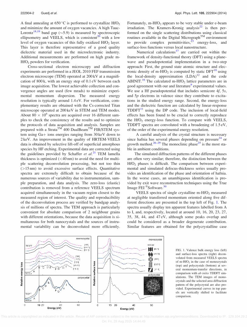
VEELS spectra of single crystalline m-HfO2 measured
at negligible transferred momentum oriented along five dif-
ferent directions are presented in the top left of Fig. 1. The
spectra usually display ten apparent features labelled from A
to I, and, respectively, located at around 10, 16, 20, 23, 27,
35, 38, 44, and 47 eV, although some peaks overlap and
could be considered as a broader degenerate contribution.
Similar features are obtained for the polycrystalline case
FIG. 1. Valence bulk energy loss (left)
and surface-loss spectra (right) decon-
voluted from measured VEELS spectra
of m-HfO2 in the case of monocrystals
(top) and polycrystals (bottom) at sev-
eral momentum-transfer directions, in
comparison with ab initio TDDFT sim-
ulations. The TEM images of mono-
crystals and the selected area diffraction
pattern of the polycrystal are also pro-
vided. Experimental curves in top pan-
els are vertically shifted to facilitate
comparison.
222904-2 Guedj et al. Appl. Phys. Lett. 105, 222904 (2014)
This article is copyrighted as indicated in the article. Reuse of AIP content is subject to the terms at: http://scitation.aip.org/termsconditions. Downloaded to IP: 129.104.29.2
On: Fri, 28 Aug 2015 14:44:49
(bottom). The TDDFT calculation displays 5 main features
(especially evident at smaller broadening) at 8, 16, 27, 38,
and 46 eV, at positions close to the peaks A, B, E, I, and FG
by less than 2 eV (see also Fig. 2). TDDFT reveals that the
shoulder A is due to single particle transitions (O 2p ! Hf
5d), like also F and G (Hf 5p! 5d); peak B is the only real
bulk plasmon, while E and I are collective excitations.
Local-field effects severely damp peak I, which would other-
wise be the main total plasmon. Details about the theoretical
calculation and interpretation will be provided elsewhere.
Our TDDFT calculations with local-field effects can be con-
sidered the best-available simulated energy-loss spectra,
with net improvement in agreement with experiment com-
pared to previous DFT calculations31 (which did not predict
the damping of the I collective excitation).
We now analyze differences in spectra measured along
different crystal directions. The most evident change is a
modulation of the oscillator strengths of the shoulder A and,
in particular, of the plasmon B. To correctly interpret this
finding, it is important to deconvolute the surface loss func-
tions (right), since the most intense feature of the surface
losses is located around 13 eV, close to the position of the
bulk plasmon. Strong differences in surface losses may
therefore contribute to the lack of perfect congruence among
literature data.
When all parameters are well controlled, the comparison
between experiment and the TDDFT is good. Although less
pronounced than in the experiment, TDDFT confirms the
directional modulation of the plasmon. In both TDDFT and
experiment, this is the most evident effect of anisotropy, the
other changes being less obvious.
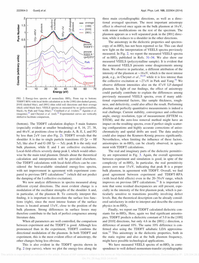
This is also evident in the TDDFT spectra shown in
Fig. 2 (top curves), where we plot the energy-loss along the
three main crystallographic directions, as well as a direc-
tional averaged spectrum. The most important anisotropy
effect is observed once again on the bulk plasmon at 16 eV,
with minor modifications on the rest of the spectrum. The
plasmon appears as a well separated peak in the [001] direc-
tion, while it reduces to a shoulder in the other directions.
The anisotropy in the dielectric properties and spectros-
copy of m-HfO2 has not been reported so far. This can shed
new light on the interpretation of VEELS spectra previously
measured. In Fig. 2, we report the measured VEELS spectra
of m-HfO2 published in Refs. 31–34. We also show our
measured VEELS (polycrystalline sample). It is evident that
the measured VEELS presents some disagreements among
them. We observe in particular, a different attribution of the
intensity of the plasmon at �16 eV, which is the most intense
peak, e.g., in Cheynet et al.,34,35 while it is less intense than
the collective excitation at �27 eV in Park and Yang.31 We
observe different intensities also on the 47 eV LF-damped
plasmon. In light of our findings, the effect of anisotropy
could partially contribute to explain the differences among
previously measured VEELS spectra, even if many addi-
tional experimental factors, like sample thickness, rough-
ness, and defectivity, could also affect the result. Performing
absolute and perfectly quantitative measurements is indeed a
real challenge. Current stability, convergence and collection
angle, energy resolution, type of measurement (EFTEM vs.
STEM), and the zero-loss removal method might have an
impact on the resulting spectra, even if perfect single scatter-
ing configurations and highly accurate corrections of aniso-
chromaticity and spatial drifts are used. The data analysis
could also impact the Kramers-Kronig process significantly.
Nevertheless, when limiting the influence of these factors,
anisotropies in m-HfO2 can be clearly observed, in agree-
ment with TDDFT calculations.
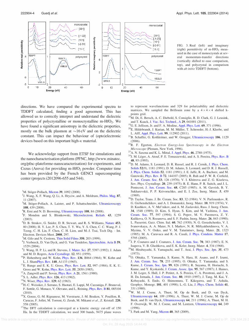
The real and imaginary parts of the dielectric permittiv-
ity are represented in Fig. 3. Again, the overall agreement
between experiment and simulation is good, in spite of the
complexity of m-HfO2. In particular, the real permittivity
passes zero near 15 eV, indicating that peak B is a proper
bulk plasmon, in agreement with TDDFT. Overall, we find
good agreement between experiment and TDDFT-RPA
(with local-field effects) even in the 20–70 eV range, which
improves on previous DFT calculations.31 It is important to
note that some residual discrepancies are still present, espe-
cially in the intensity of the first plasmon peak, which is par-
ticularly sensitive to transitions possibly involving defect
levels. But, the theoretical description can be already consid-
ered satisfactory in order to interpret and describe the correct
physics in m-HfO2.
Finally, we report our TDDFT calculated dielectric con-
stants for m-HfO2. Here, again we find significant anisotro-
pies. TDDFT predicts a dielectric constant of 5.0 in the [100]
and [010] directions, but only 4.6 in the [001] z direction, a
difference of around 10%. The same 10% difference is con-
firmed also using the TDDFT adiabatic LDA approxima-
tion.12 This anisotropy in the dielectric properties, both in
the static regime and also at the bulk plasmon frequency,
might have possible technological applications.
We have measured VEELS spectra of m-HfO2 in corre-
spondence to well defined momentum-transfer crystallographic
FIG. 2. Energy-loss spectra of monoclinic HfO2. From top to bottom:
TDDFT RPA with local fields calculation as in the [100] (dot-dashed green),
[010] (dashed blue), and [001] (thin solid red) directions and their average
(thick solid black line); VEELS spectra as measured by us (polycrystalline,
black), by Park and Yang (blue),31 Couillard et al. (violet),32 Agustin et al.(magenta),33 and Cheynet et al. (red).34 Experimental curves are vertically
shifted to facilitate comparison.
222904-3 Guedj et al. Appl. Phys. Lett. 105, 222904 (2014)
This article is copyrighted as indicated in the article. Reuse of AIP content is subject to the terms at: http://scitation.aip.org/termsconditions. Downloaded to IP: 129.104.29.2
On: Fri, 28 Aug 2015 14:44:49
directions. We have compared the experimental spectra to
TDDFT calculated, finding a good agreement. This has
allowed us to correctly interpret and understand the dielectric
properties of polycrystalline or monocrystalline m-HfO2. We
have found a significant anisotropy in the dielectric properties,
mostly on the bulk plasmon at �16 eV and on the dielectric
constant. This can impact the behaviour of (opto)electronic
devices based on this important high-j material.
We acknowledge support from ETSF for simulations and
the nanocharacterisation platform (PFNC, http://www.minatec.
org/pfnc-plateforme-nanocaracterisation) for experiments, and
Cezus (Areva) for providing m-HfO2 powder. Computer time
has been provided by the French GENCI supercomputing
center (projects i2012096-655 and 544).
1M. St€oger-Pollach, Micron 39, 1092 (2008).2J. Wang, X. F. Wang, Q. Li, A. Hryciw, and A. Meldrum, Philos. Mag. 87,
11 (2007).3M. St€oger-Pollach, A. Laister, and P. Schattschneider, Ultramicroscopy
108, 439 (2008).4R. Erni and N. D. Browning, Ultramicroscopy 108, 84 (2008).5F. Mondon and S. Blonkowski, Microelectron. Reliab. 43, 1259
(2003).6D. B. Strukov, G. Snider, D. R. Stewart, and R. S. Williams, Nature 453,
80 (2008); H. Y. Lee, P. S. Chen, T. Y. Wu, Y. S. Chen, C. C. Wang, P. J.
Tzeng, C. H. Lin, F. Chen, C. H. Lien, and M.-J. Tsai, Tech Dig. - Int.
Electron. Devices Meet. 2008, 297.7M. Gilo and N. Croitoru, Thin Solid Films 350, 203 (1999).8J. Verbeeck, D. Van Dyck, and G. Van Tendeloo, Spectrochim. Acta B 59,
1529 (2004).9J. Wang, H. P. Li, and R. Stevens, J. Mater. Sci. 27, 5397 (1992); J. Adam
and M. D. Rogers, Acta Crystallogr. 12, 951 (1959).10P. Hohenberg and W. Kohn, Phys. Rev. 136, B864 (1964); W. Kohn and
L. J. ShamPhys. Rev. 140, A1133 (1965).11E. Runge and E. K. U. Gross, Phys. Rev. Lett. 52, 997 (1984); E. K. U.
Gross and W. Kohn, Phys. Rev. Lett. 55, 2850 (1985).12A. Zangwill and P. Soven, Phys. Rev. A 21, 1561 (1980).13S. L. Adler, Phys. Rev. 126, 413 (1962).14N. Wiser, Phys. Rev. 129, 62 (1963).15H.-C. Weissker, J. Serrano, S. Huotari, E. Luppi, M. Cazzaniga, F. Bruneval,
F. Sottile, G. Monaco, V. Olevano, and L. Reining, Phys. Rev. B 81, 085104
(2010).16X. Gonze, G.-M. Rignanese, M. Verstraete, J.-M. Beuken, Y. Pouillon, R.
Caracas, F. Jollet, M. Torrent, G. Zerah, M. Mikami et al., Z. Kristall. 220,
558 (2005).17The DFT calculation is converged at a kinetic energy cut-off of 150
Ha. In the TDDFT calculation, we used 300 bands, 9475 plane waves
to represent wavefunctions and 329 for polarizability and dielectric
matrices. We sampled the Brillouin zone by a 4� 4� 4 shifted k-
points grid.18M. Di, E. Bersch, A. C. Diebold, S. Consiglio, R. D. Clark, G. J. Leusink,
and T. Kaack, J. Vac. Sci. Technol., A 29, 041001 (2011).19G. E. Jellison, Jr. and F. A. Modine, Appl. Phys. Lett. 69, 371 (1996).20E. Hildebrandt, J. Kurian, M. M. M€uller, T. Schroeder, H.-J. Kleebe, and
L. Alff, Appl. Phys. Lett. 99, 112902 (2011).21B. Schaffer, G. Kothleitner, and W. Grogger, Ultramicroscopy 106, 1129
(2006).22R. F. Egerton, Electron Energy-loss Spectroscopy in the Electron
Microscope (Plenum, New York, 1996).23A. N. Saxena and K. L. Mittal, J. Appl. Phys. 46, 2788 (1975).24J. M. L�eger, A. Atouf, P. E. Tomaszewski, and A. S. Pereira, Phys. Rev. B
48, 93 (1993).25D. M. Adams, S. Leonard, D. R. Russel, and R. J. Cernik, J. Phys. Chem.
Solids 52(9), 1181 (1991); D. M. Adams, S. Leonard, and D. R. J. Russell,
J. Phys. Chem. Solids 52, 1181 (1991); J. E. Jaffe, R. A. Bachorz, and M.
Gutowski, Phys. Rev. B 72, 144107 (2005); R. Ruh and P. W. R. Corfield,
J. Am. Ceram. Soc. 53, 126 (1970); V. I. Khitrova and Z. G. Kiseleva,
Sov. Phys. Crystallogr. 20, 239 (1975); R. E. Hann, P. R. Suitch, and J. L.
Pentecost, J. Am. Ceram. Soc. 68, C285 (1985); A. M. Gavrish, B. Y.
Sukharevskii, P. P. Krivoruchko, and E. I. Zoz, Inorg. Mater. 5, 459
(1969).26D. Taylor, Trans. J. Br. Ceram. Soc. 83, 32 (1984); V. N. Parfenenkov, R.
G. Grebenshchikov, and A. I. Domanskii, Inorg. Mater. 10, 919 (1974); V.
D. Kushkov, A. V. Mel’nikov, and A. M. Zaslavskii, Russ. J. Inorg. Chem.
34, 1548 (1989); D. Kim, S. Hyun, S. Kim, and M. Yashima, J. Am.
Ceram. Soc. 77, 597 (1994); S. G. Popov, M. V. Paromova, Z. Y.
Kulikova, O. N. Rozanova, and S. F. Pashin, Inorg. Mater. 26, 843 (1990);
L. Passerini, Gazz. Chim. Ital. 60, 762 (1930); N. G. Gorashchenko, V. I.
Ivanovskaya, A. A. Maier, N. I. Markov, N. R. Miftyakhetdinova, V. A.
Myzina, V. V. Osiko, and V. M. Tatarintsev, Inorg. Mater. 21, 1323
(1985); M. A. Caravaca and R. A. Casali, J. Phys. Condens. Matter 17,
5795 (2005).27J. P. Coutures and J. Coutures, J. Am. Ceram. Soc. 70, 383 (1987); E. N.
Isupova, V. B. Glushkova, and E. K. Keler, Inorg. Mater. 4, 334 (1968).28M. Hirabayashi, S. Yamaguchi, and T. Arai, J. Phys. Soc. Jpn. 35, 473
(1973).29O. Ohtaka, T. Yamanaka, S. Kume, N. Hara, H. Asano, and F. Izumi,
J. Am. Ceram. Soc. 78, 233 (1995); O. Ohtaka, T. Yamanaka, and S.
Kume, J. Ceram. Soc. Jpn. 99, 826 (1991); R. Suyama, H. Horiuchi, S.
Kume, and Y. Kyokaishi, J. Ceram. Assoc. Jpn. 95, 567 (1987); J. Haines,
J. M. Leger, S. Hull, J. P. Petitet, A. S. Pereira, C. A. Perottoni, and J. A.
H. Da Jornada, J. Am. Ceram. Soc. 80, 1910 (1997); J. Tang, M. Kai, Y.
Kobayashi, S. Endo, O. Shimomura, T. Kikegawa, and T. Ashida,
Geophys. Monogr. 101, 401 (1998); L.-G. Liu, J. Phys. Chem. Solids 41,
331 (1980).30W. M. J. Coene, A. Thust, M. Op de Beek, and D. van Dyck,
Ultramicroscopy 64, 109 (1996); A. Thust, W. M. J. Coene, M. Op de
Beek, and D. van Dyck, Ultramicroscopy 64, 211 (1996); A. Thust, M. H.
F. Overwijk, W. M. J. Coene, and M. Lentzen, Ultramicroscopy 64, 249
(1996).31J. Park and M. Yang, Micron 40, 365 (2009).
FIG. 3. Real (left) and imaginary
(right) permittivity of m-HfO2 meas-
ured in the case of monocrystals at sev-
eral momentum-transfer directions
(vertically shifted to ease comparison,
top), and polycrystal in comparison
with ab initio TDDFT (bottom).
222904-4 Guedj et al. Appl. Phys. Lett. 105, 222904 (2014)
This article is copyrighted as indicated in the article. Reuse of AIP content is subject to the terms at: http://scitation.aip.org/termsconditions. Downloaded to IP: 129.104.29.2
On: Fri, 28 Aug 2015 14:44:49

32M. Couillard, M. Kociak, O. Stephan, G. A. Botton, and C. Colliex, Phys.
Rev. B 76, 165131 (2007).33M. P. Agustin, L. R. C. Fonseca, J. C. Hooker, and S. Stemmer, Appl.
Phys. Lett. 87, 121909 (2005).
34M. C. Cheynet, S. Pokrant, F. D. Tichelaar, and J.-L. Rouviere, J. Appl.
Phys. 101, 054101 (2007).35C. C. Ahn, O. Krivanek, R. P. Burgner, M. M. Disko, and P. R. Swann,
EELS Atlas (Gatan, Warrendale, 1983).
222904-5 Guedj et al. Appl. Phys. Lett. 105, 222904 (2014)
This article is copyrighted as indicated in the article. Reuse of AIP content is subject to the terms at: http://scitation.aip.org/termsconditions. Downloaded to IP: 129.104.29.2
On: Fri, 28 Aug 2015 14:44:49


![Monoclinic polymorph of poly[aqua(μ 4 -hydrogen tartrato)sodium]](https://static.fdokumen.com/doc/165x107/63460bb1596bdb97a9093600/monoclinic-polymorph-of-polyaquam-4-hydrogen-tartratosodium.jpg)