Evaluation of DC supply protection for efficient energy delivery ...
113
HAL Id: tel-01797803 https://tel.archives-ouvertes.fr/tel-01797803 Submitted on 22 May 2018 HAL is a multi-disciplinary open access archive for the deposit and dissemination of sci- entific research documents, whether they are pub- lished or not. The documents may come from teaching and research institutions in France or abroad, or from public or private research centers. L’archive ouverte pluridisciplinaire HAL, est destinée au dépôt et à la diffusion de documents scientifiques de niveau recherche, publiés ou non, émanant des établissements d’enseignement et de recherche français ou étrangers, des laboratoires publics ou privés. Evaluation of DC supply protection for effcient energy delivery in low voltage applications Thi Thuong Huyen Ma To cite this version: Thi Thuong Huyen Ma. Evaluation of DC supply protection for effcient energy delivery in low voltage applications. Electric power. Université de Lyon, 2018. English. NNT : 2018LYSE1055. tel-01797803
-
Upload
khangminh22 -
Category
Documents
-
view
0 -
download
0
Transcript of Evaluation of DC supply protection for efficient energy delivery ...
HAL Id: tel-01797803https://tel.archives-ouvertes.fr/tel-01797803
Submitted on 22 May 2018
HAL is a multi-disciplinary open accessarchive for the deposit and dissemination of sci-entific research documents, whether they are pub-lished or not. The documents may come fromteaching and research institutions in France orabroad, or from public or private research centers.
L’archive ouverte pluridisciplinaire HAL, estdestinée au dépôt et à la diffusion de documentsscientifiques de niveau recherche, publiés ou non,émanant des établissements d’enseignement et derecherche français ou étrangers, des laboratoirespublics ou privés.
Evaluation of DC supply protection for efficient energydelivery in low voltage applications
Thi Thuong Huyen Ma
To cite this version:Thi Thuong Huyen Ma. Evaluation of DC supply protection for efficient energy delivery in lowvoltage applications. Electric power. Université de Lyon, 2018. English. �NNT : 2018LYSE1055�.�tel-01797803�
N°d’ordre NNT : 2018LYSE1055
THESE de DOCTORAT DE L’UNIVERSITE DE LYON opérée au sein de
l’Université Claude Bernard Lyon 1
Ecole Doctorale N° 160 Électronique, Électrotechnique, Automatique de Lyon (EEA)
Spécialité de doctorat : Génie electrique
Soutenue publiquement le 05 april 2018, par: Thi Thuong Huyen MA
Evaluation of DC supply protection for efficient energy delivery in low voltage
applications Devant le jury composé de:
M. SECHILARIU Manuela Professeure, Université de Technologie de Compiègne Rapporteur
M. PHAN Xuan Minh Professeure, Institut Polytechnique de Hanoï Rapporteur
M. LU Guo Neng Professeur, Université Claude Bernard Lyon 1 Examinateur
M. YAHOUI Hamed Maître de Conférences-HDR Université Claude Bernard Lyon 1
Directeur de thèse
M. HERVÉ Morel Directeur de Recherche CNRS, Ampere Invité
UNIVERSITE CLAUDE BERNARD - LYON 1 Président de l’Université
Président du Conseil Académique
Vice-président du Conseil d’Administration
Vice-président du Conseil Formation et Vie Universitaire
Vice-président de la Commission Recherche
Directrice Générale des Services
M. le Professeur Frédéric FLEURY
M. le Professeur Hamda BEN HADID
M. le Professeur Didier REVEL
M. le Professeur Philippe CHEVALIER
M. Fabrice VALLÉE
Mme Dominique MARCHAND
COMPOSANTES SANTE
Faculté de Médecine Lyon Est – Claude Bernard
Faculté de Médecine et de Maïeutique Lyon Sud – Charles Mérieux
Faculté d’Odontologie
Institut des Sciences Pharmaceutiques et Biologiques
Institut des Sciences et Techniques de la Réadaptation
Département de formation et Centre de Recherche en Biologie Humaine
Directeur : M. le Professeur G.RODE
Directeur : Mme la Professeure C. BURILLON
Directeur : M. le Professeur D. BOURGEOIS
Directeur : Mme la Professeure C. VINCIGUERRA
Directeur : M. X. PERROT
Directeur : Mme la Professeure A-M. SCHOTT
COMPOSANTES ET DEPARTEMENTS DE SCIENCES ET TECHNOLOGIE
Faculté des Sciences et Technologies
Département Biologie
Département Chimie Biochimie
Département GEP
Département Informatique
Département Mathématiques
Département Mécanique
Département Physique
UFR Sciences et Techniques des Activités Physiques et Sportives
Observatoire des Sciences de l’Univers de Lyon
Polytech Lyon
Ecole Supérieure de Chimie Physique Electronique
Institut Universitaire de Technologie de Lyon 1
Ecole Supérieure du Professorat et de l’Education
Institut de Science Financière et d'Assurances
Directeur : M. F. DE MARCHI
Directeur : M. le Professeur F. THEVENARD
Directeur : Mme C. FELIX
Directeur : M. Hassan HAMMOURI
Directeur : M. le Professeur S. AKKOUCHE
Directeur : M. le Professeur G. TOMANOV
Directeur : M. le Professeur H. BEN HADID
Directeur : M. le Professeur J-C PLENET
Directeur : M. Y.VANPOULLE
Directeur : M. B. GUIDERDONI
Directeur : M. le Professeur E.PERRIN
Directeur : M. G. PIGNAULT
Directeur : M. le Professeur C. VITON
Directeur : M. le Professeur A. MOUGNIOTTE
Directeur : M. N. LEBOISNE
i
ABSTRACT
Currently, there is a drop in the price of distributed energy resources, especially solar PVs, which leads to a significant growth of the installed capacities in many countries. On the other hand, policies encouraging energy efficiency have promoted the development of DC loads in domestic areas, such as LEDs lighting, computers, telephones, televisions, efficient DC motors and electric vehicles. Corresponding to these changes in sources and loads, DC microgrid distribution system becomes more attractive than the traditional AC distribution system. The main advantages of the DC microgrid are higher energy efficiency, easier in integrating with distributed energy sources and storage systems. While many studies concentrate on the control strategies and energy management in the DC microgrid, the protection still receives inadequate attention and lack of regulations and experiences. Protection in DC grids is more complex than AC grids due to the continuous arc, higher short circuit current value and fault rate of rising. Furthermore, the DC distributed grids are composed of many electronic and semiconductor switching devices, which only sustain the fault currents of some tens of microseconds. Mechanical circuit breakers, which have a response time in tens of milliseconds, seem not to meet the safety requirement of DC microgrids. The lack of effective protection devices is a barrier to the development of DC microgrids in the distributed systems.
This thesis proposes a self-power solid-state DC circuit breaker using normally-on SiC JFET, which offers a great protection device for DC microgrids due to its fast response time and low on-state losses. The design of the solid state DC circuit breaker aims to meet two objectives: fast response time and high reliability. The designed specifications and critical energies that result in the destruction of the circuit breaker are identified on the basis of the experiments of a commercial normally-on JFET. In addition, a very fast and reliable protection driver based on a forward-flyback converter topology is employed to generate a sufficient negative voltage to turn and hold off the SiC JFET. The converter will be activated whenever short-circuit faults are detected by sensing the drain-source voltage, then creating a negative voltage applied to the gate of JFET. To avoid gate failure by overvoltage at the gate of JFET, the output voltage of the forward-flyback converter is regulated using Primary Side Sensing technique. Experimental results validated the working principle of the proposed solid state DC circuit breaker with fault clearing time less than 3 μs.Additionally, a model of the normally-on JFET in Matlab/Simulink environment is built for exploring the behaviors of the solid-state DC circuit breaker during short-circuit faults. The agreement between the simulation and experimental results confirms that this JFET model can be appropriately used for the investigation of solid state DC circuit breaker operations and DC microgrids in general during fault evens and clearing fault processes.
Keywords: DC circuit breaker, DC microgrid, normally-on SiC JFET, protection in DC microgrid, robustness of SiC JFET, short circuit protection, solid-state DC circuit breaker.
ii
RESUME
Actuellement, il y a une baisse du prix des ressources énergétiques distribuées, en particulier l'énergie solaire photovoltaïque, conduisant à la croissance significative de leur capacité d’installation dans de nombreux pays. D'autre part, les politiques encourageant l'efficacité énergétique ont favorisé le développement de charges DC dans les zones domestiques, telles que l'éclairage LED, les ordinateurs,, les téléphones, les téléviseurs, les moteurs DC efficaces et les véhicules électriques. Grace àce changement, le système de distribution de microgrid DC devient plus attractive que le système de distribution à courant alternatif traditionnel. Les avantages principaux du microgrid DC sont l’efficacité énergétique plus élevée, plus facile à intégrer avec les sources d'énergie distribuées et le système de stockage.
Alors que de nombreuses recherches se concentrent sur les stratégies de contrôle et la gestion de l'énergie dans le microgrid DC, sa protection reçoit une attention insuffisante et un manque de réglementation et d'expériences. La protection dans les réseaux DC est plus difficile que dans le réseau AC en raison de l'arc continu, de la valeur plus élevée du courant de court-circuit et du taux de défaut de montée. En outre, dans les réseaux distribués à courant continu sont composés de nombreux dispositifs de commutation électroniques et semi-conducteurs, qui ne supportent le courant de défaut que quelques dizaines de microsecondes. Les disjoncteurs mécaniques, qui ont un temps de réponse de quelques dizaines de millisecondes, ne semblent pas satisfaire aux exigences de sécurité du microréseau à courant continu. L'absence d'un dispositif de protection efficace constitue un obstacle au développement du microgrid DC dans le système distribué.Cette thèse propose un disjoncteur DC auto-alimenté à courant continu utilisant normalement JFET SiC, qui offre un excellent dispositif de protection pour les microgrids DC grâce à son temps de réponse rapide et ses faibles pertes à l'état passant. La conception du disjoncteur DC à semi-conducteurs vise à répondre à deux objectifs: temps de réponse rapide et fiabilité. Les spécifications conçues et les énergies critiques qui entraînent la destruction du disjoncteur sont identifiées sur la base des résultats mesurés d'un JFET populaire dans le commerce. Un pilote de protection très rapide et fiable basé sur une topologie à convertisseur flyback avant est utilisé pour générer une tension négative suffisante pour tourner et maintenir le JFET SiC. Le convertisseur sera activé chaque fois que le disjoncteur détecte des défauts de court-circuit en détectant la tension de drain-source de JFET et crée une tension négative s'applique à la porte de JFET. Pour éviter une défaillance de la porte par surtension au niveau de la grille du JFET, la tension de sortie du convertisseur de retour vers l'avant est régulée à l’aide de la mesure coté primaire. Les résultats expérimentaux sur le prototype du disjoncteur DC ont validé les principes de fonctionnement proposés et ont confirmé que le disjoncteur DC à semi-conducteurs proposé peut interrompre le défaut en 3 μs. D'un autre côté, un modèle du JFET normalement activé dans l'environnement Matlab/Simulink est construit pour étudier les comportements du SSCB pendant une durée de court-circuit. L'accord entre la simulation et les résultats expérimentaux confirment que ce modèle JFET peut être utilisé pour simuler le fonctionnement d'un disjoncteur DC et dans l'étude du fonctionnement du microgrid DC pendant le processus de défaut et de compensation.
Mots-clés: Disjoncteur DC, microgrid DC, JFET SiC normally-on, protection en microgrid DC, robustesse du JFET SiC, protection contre les courts-circuits, disjoncteur à semi-conducteurs.

iii
ACKNOWLEDGEMENTS
This doctoral thesis concludes the major part of the work, which I have carried out at the Laboratory Ampere, Claude Bernard Lyon 1 University since November 2015. I would never have had the strength to pursue this work successfully without the guidance, encouragement, help, and support of various persons. First of all, I would like to express my sincere gratitude to my supervisor, Assoc. Prof Hamed Yahoui, for his patient guidance, enthusiastic encouragement and useful advice of this research work. His wide knowledge and his way of thinking have been of great value to me. Without him, being my supervisor, this thesis would never be a complete piece of work. I also would like to express my great appreciation to Dr. Hervé Morel for the immense contribution to the success of this work. Under his supervision, I have gained a lot of knowledge and experience in semiconductor devices and methods to investigate their characteristics. From him, I have learned how to work as a research scientist. Special thanks go to Dr. Hoang Giang VU from Electric Power University, Vietnam. He is not only my supervisor but also a good friend, and a colleague. Without his precious support, it would not be possible to conduct this research. I also would like to give many thanks to Dr. Nicolas Siauvé for his supporting on various fields at the laboratory. It was a pleasure to work under the supervision of all four of you.
I would like to express my sincere gratitude to Glink project-Erasmus Mundus program for supporting and providing the funding for the work. A very special gratitude goes to GENOME project for allowing me using the short circuit and avalanche test bench, hence I can quickly complete the complex tests with JFET.
My grateful thanks are also extended to the labmates and staff at the Ampere laboratory and the Genie Electric department. Thank you for the great working environment and your assistance. A special thank goes to Fedia Baccar El Boubkari and Thanh Kha Tran for the great collaboration. I also want to particularly thank Lea Chancelier and Ewelina Bolimowska for all the assistance during the time preparing and staying in Lyon. My time at Lyon was enriched due to many Vietnamese friends who are like me living away from home. I am grateful for the time we share the happiness, sadness, and difficulty with each other during last three years.
Last but not least, I would like to thank my family for all their love, encouragement and support. Most of all I want to thank my husband and our beloved daughters who are the biggest supporters and motivation for me to complete this work.
Lyon, December 2017
MA Thi Thuong Huyen

iv iv
TABLE OF CONTENTS
Abstract ...................................................................................................................................... i
Résumé ...................................................................................................................................... ii Acknowledgements ................................................................................................................. iii
Table of contents ..................................................................................................................... iv List of figures .......................................................................................................................... vii
List of abbreviations ............................................................................................................... xi General introduction ............................................................................................................... 1
Energy consumption in domestic field ............................................................................... 1 Current status of energy consumption in buildings ........................................................... 1 Policies to promote energy efficiency................................................................................ 1The increase of renewable energy sources ......................................................................... 2 The development of DC Loads .......................................................................................... 3 Why a DC microgrid? ........................................................................................................ 3
Motivations ........................................................................................................................... 4 Research objectives and approach ..................................................................................... 4
Link with the ANR C3μ project ......................................................................................... 4 Research Objectives and Thesis Outline ............................................................................ 5
CHAPTER 1: State of the art in dc microgrid protection .................................................. 7 1.1 Introduction .................................................................................................................... 7 1.2 Short circuit and protection in DC microgrids ........................................................... 7
1.2.1 Concept and structures of DC microgrids .............................................................. 7 1.2.2 Challenges of short circuits in DC microgrid ......................................................... 10
1.2.2.1 Characteristics of short circuit in DC microgrid .............................................. 10 1.2.2.2 Interruption of short circuit current in DC grid ............................................... 12
1.2.3 Requirements of a DC Circuit Breaker in the DC Microgrid ............................... 13 1.2.4 Comparison of protective devices technologies for DC grid .................................. 13
1.3 Solid state DC circuit breakers ................................................................................... 17 1.3.1 Topologies for solid state DC circuit breakers .................................................... 17 1.3.2 Power Semiconductor Devices in Solid-State Circuit Breakers .......................... 19
1.3.2.1 Electrical properties ......................................................................................... 201.3.2.2 Comparison of semiconductor materials ......................................................... 23 1.3.2.3 Structure of SiC devices ................................................................................... 23
1.3.3 Reliability of Solid State circuit breakers ............................................................. 26 1.3.3.1 Destruction mechanisms of SiC semiconductor devices ................................. 26 1.3.3.2 Robustness of SiC devices in avalanche mode ................................................ 27 1.3.3.3 Robustness of SiC device in short circuit mode .............................................. 29 1.3.3.4 Aging of SiC devices under short circuits ....................................................... 32
1.3.4 The advantages of normally-on SiC JFETs for Solid-State circuit breaker applications ...................................................................................................................... 34
1.4 Conclusions ................................................................................................................ 35
CHAPTER 2: Characteristics of normally-on SiC JFETs ............................................... 37 2.1 Introduction .................................................................................................................. 37 2.2 Measurement characteristics of the normally-on SiC JFET ................................... 38
2.2.1 Power device analyzer for parameter identification ............................................... 38 2.2.2 Static characteristics ................................................................................................ 39 2.2.3 Transfer characteristics ........................................................................................... 40

v v
2.2.4 On-state resistance .................................................................................................. 41 2.2.5 Leakage current measurement ................................................................................ 42 2.2.6 Dynamic characteristics .......................................................................................... 42 2.2.7 Switching characteristics ........................................................................................ 46
2.3 Robustness of normally-on SiC JFET ........................................................................ 48 2.3.1 Short Circuit and Avalanche Breakdown Test Bench ............................................ 48 2.3.2 Robustness of SiC JFET in the short-circuit mode................................................. 50
2.3.2.1 Description of short-circuit test bench ............................................................. 50 2.3.2.2 Drive signal in short circuit operations ............................................................ 51 2.3.2.3 Calculation of critical energy in short circuit mode ......................................... 52 2.3.2.4 Failure modes of SiC JFET in short-circuit tests ............................................. 52
2.3.3 Robustness of SiC JFET in the avalanche mode .................................................... 59 2.3.3.1 Description of the avalanche test bench ........................................................... 59 2.3.3.2 Failures of normally-on SiC JFET in avalanche mode .................................... 60
2.4 Conclusions ................................................................................................................... 61
CHAPTER 3: Solid state DC circuit breaker based on normally-on SiC JFETs ........... 63 3.1 Introduction.................................................................................................................. 633.2 Topologies and main components of the solid state DC circuit breaker based on normally-on SiC JFETs ..................................................................................................... 64 3.3 Operating principle ...................................................................................................... 67
3.3.1 Concept of self-powered solid-state circuit breaker ............................................ 67 3.3.2 The operation of the protection driver ................................................................. 67 3.3.3 Gate voltage limitation principle .......................................................................... 71
3.4 Simulations of normally-on SiC JFET and protective function ............................. 72 3.4.1 Mathematical model of the normally-on SiC JFET ............................................. 73
3.4.1.1 Static model .................................................................................................... 73 3.4.1.2 Dynamic model .............................................................................................. 743.4.1.3 Temperature dependence ................................................................................ 74 3.4.1.4 Extraction of parameters ................................................................................. 75
3.4.2 Matlab/Simulink model ........................................................................................ 76 3.4.3 Validation of the SiC JFET model ....................................................................... 77
3.4.3.1 Validation of static characteristic ..................................................................... 77 3.4.3.2 Validation of dynamic characteristic ............................................................... 77
3.4.4 Application in DC circuit breaker with normally-on SiC JFET ............................. 79 3.5 Prototype design of the solid-state circuit breaker based on SiC JFETs ............ 81
3.5.1 Design of forward-flyback converter for self-powered solid-state circuit breaker81
3.5.1.1 Design specifications of the forward-flyback converter .................................. 81 3.5.1.2 Design of forward-flyback transformer ........................................................... 82
3.5.2 Selection of components of voltage sensor ............................................................. 84 3.6 Experimental validation .............................................................................................. 85
3.6.1 Gate voltage limitation function of the forward-flyback converter ........................ 85 3.6.2 Operation of the voltage sensor .............................................................................. 86 3.6.3 Operation of the converter driving the JFET .......................................................... 87
3.7 Conclusions ................................................................................................................ 88
Conclusions and perspectives ................................................................................................ 89 Conclusions......................................................................................................................... 89Perspectives ........................................................................................................................ 90
The affection of the temperature to the operation of solid-state circuit breaker .............. 90 Challenges regarding parallel connection of SiC JFETs. ................................................ 91
Publications ............................................................................................................................ 92

vi vi
BIBLIOGRAPHY .................................................................................................................. 93
vii vii
LIST OF FIGURES
Figure 0-1 Final energy consumption breakdown into sectors in the EU-27, 2010 [2] ............. 1
Figure 0-2 Final electricity consumption breakdown into sectors in the EU-27, 2010 [2] ....... 2Figure 1-1 Unipolar single bus DC microgrid [22] ................................................................... 8
Figure 1-2 A bipolar single bus DC microgrid [22] .................................................................. 8Figure 1-3 A typical DC microgrid configuration utilizes DC circuit breakers ........................ 9
Figure 1-4 Ring bus DC microgrid [22] .................................................................................... 9Figure 1-5 Two types of short circuit faults in DC systems: (a) pole-to-ground fault, (b) pole-
to-pole fault. ..................................................................................................................... 10Figure 1-6 Equivalent short circuit diagram of one DC source ............................................... 11
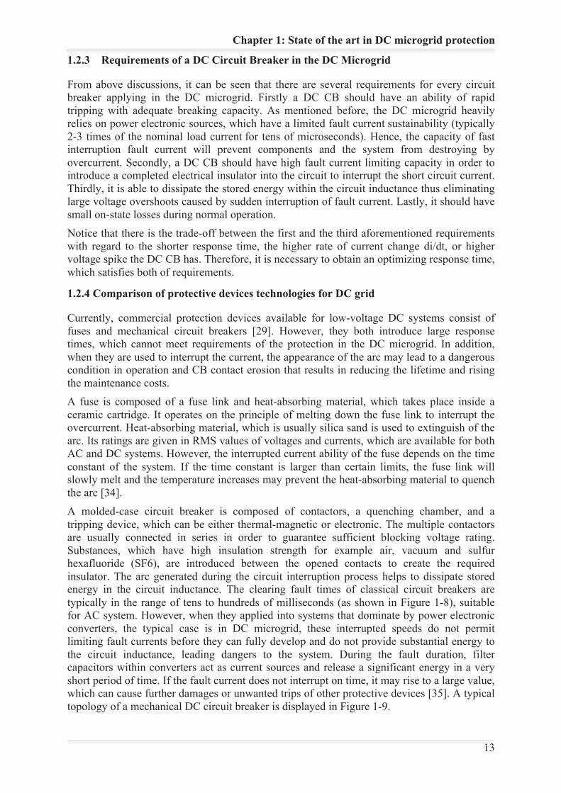
Figure 1-7 Basic DC circuit containing a circuit breaker with short circuit fault.................... 12Figure 1-8 Example of a typical time-current characteristic curve of a thermal-magnetic
trigger system for a mechanical circuit breaker [33] ....................................................... 14Figure 1-9 Basic structure of the mechanical DC circuit breaker [37] .................................... 15
Figure 1-10 Basic structure of solid state DC circuit [37] ....................................................... 15Figure 1-11 Basic structure of hybrid DC circuit [37] ............................................................. 16
Figure 1-12 A generic bidirectional solid state DC breaker schematic diagram [36] ............. 18Figure 1-13 Unidirectional self-power SSCB using normally-on SiC JFET [40] ................... 19
Figure 1-14 Bidirectional self-power SSCB using normally-on SiC JFET [41] ..................... 19Figure 1-15 Intrinsic carrier for various semiconductors VS reciprocal temperature [44] ...... 20
Figure 1-16 Electric field and potential distribution for an abrupt parallel-plane P+/N junction .......................................................................................................................................... 21
Figure 1-17 Maximal doping level vs. theoretical breakdown voltage for several semiconductor materials [43], [44] .................................................................................. 21
Figure 1-18 Thermal runaway limits for various semiconductor materials [45] ..................... 22Figure 1-19 Theoretical specific resistance of the epilayer as a function of breakdown voltage
at 600 K [44] .................................................................................................................... 22Figure 1-20 SiCED Normally-on LVJFET (a) optimized for fast switching (b) optimized for
low on-state resistance [47] ............................................................................................. 24Figure 1-21 SemiSouth (a) normally-on and (b) normally-off V-JFET [50] ........................... 25
Figure 1-22 (a) Cross-section of U-MOSFET and (b) Cross-section of D-MOSFET [47] ..... 25Figure 1-23 Simplified device cross section of a SiC power BJT with a two-zone etched [52]
.......................................................................................................................................... 26Figure 1-24 Schematic of Unclamped Inductive Switching test for Avalanche mode [52] .... 27Figure 1-25 VDS and ID of normally-off JFET in avalanche mode [52] .................................. 27
Figure 1-26 Destructive test of normally-on SiC JFET in avalanche mode [52] .................... 28Figure 1-27 VDS and IDS of MOSFET in avalanche mode [52] ............................................... 28
Figure 1-28 Destructive test of BJT in avalanche mode: (a) collector-emitter voltage and
viii viii
collector current, (b) base-emitter voltage and base current [52] .................................... 29
Figure 1-29 Schematic of short-circuit test [53] ...................................................................... 29Figure 1-30 Destructive test for normally-on JFET in current limitation mode (VDC=400 V,
TCASE=250C) [54] ............................................................................................................. 30Figure 1-31 Estimation of the temperature during a long term short circuit phase (VDC=400 V,
TCASE=250C) [54] ............................................................................................................. 30Figure 1-32 Robustness of normally-off JFET under long-term short-circuit test [55] .......... 31
Figure 1-33 Destructive test of a CMF20120D MOSFET (a) Drain and (b) Gate waveform for VDC=600V and T=250C [56] ............................................................................................ 31
Figure 1-34 Destructive test of SiC BJT in short circuit [52] .................................................. 31Figure 1-35 Evolution of drain current with drain-source voltage for VGS=0 V, during aging
of 100 mΩ SiC JFET (aging test conditions: E = 540V, Tsc = 100 μs, TC = 25 0C) [58] 32Figure 1-36 Evolution of drain current with drain - source voltage (VGS =0V) during aging of
300 mΩ SiC JFET (aging test conditions: E = 540 V, Tsc = 200 μs, TC = 25 0C) [58] .... 33Figure 1-37 (a) Gate current, (b) room in gate current (c) gate-source voltage and (d) drain
current of SiC MOSFET during repetitive short circuit, with tsc = 3 μs, TC = 25 0C [52] 33Figure 1-38 (a) Gate current, (b) room in gate current (c) gate-source voltage and (d) drain
current of SiC MOSFET during repetitive short circuit, with tsc = 7 μs, TC = 25 0C [52] 34Figure 2-1 Cross section of the normally-on vertical SiC JFET [62] ...................................... 38
Figure 2-2 Photograph of B1506A power device analyzer for circuit design from Keysight Technology [64] ............................................................................................................... 38
Figure 2-3 Static characteristics of UJN 1205K JFET at TCASE = 25 0C ................................. 39Figure 2-4 Identify the current limiting value for solid state circuit breaker ........................... 40
Figure 2-5 Transfer characteristics of UJN 1205K JFET at VDS = 5 V, TCASE = 25 0C and TCASE = 175 0C ................................................................................................................. 40
Figure 2-6 Typical drain-source resistance of UJN 1205K JFET at VGS = 0 V, TCASE = 25 0C.......................................................................................................................................... 41
Figure 2-7 Typical drain-source leakage current of UJN 1205K JFET at VGS = -20 V, TCASE = 25 0C ................................................................................................................................. 42
Figure 2-8 Schematic diagram of a normally-on SiC JFET (a) with drain-source capacitance and (b) without drain-source capacitance ........................................................................ 43
Figure 2-9 Circuit diagram to measure Ciss ............................................................................ 43Figure 2-10 Circuit diagram to measure Coss ......................................................................... 44
Figure 2-11 Circuit diagram to measure Crss .......................................................................... 44Figure 2-12 Typical capacitances of UJN 1205K JFET at 100 kHz, TCASE = 25 0C ............... 45
Figure 2-13 Variation of gate-source capacitance to drain-source voltage of UJN 1205K JFET at f = 100 kHz, TCASE = 25 0C.......................................................................................... 45
Figure 2-14 Variation of gate-drain capacitance to drain-source voltage of UJN 1205K JFET at f = 100 kHz, TCASE = 25 0C .......................................................................................... 46
Figure 2-15 Variation of drain-source capacitance to drain-source voltage of UJN 1205K JFET at f = 100 kHz, TCASE = 25 0C ................................................................................ 46
ix ix
Figure 2-16 Unclamped Inductive Switching test circuit ........................................................ 47
Figure 2-17 Unclamped Inductive Switching test bench ......................................................... 47Figure 2-18 Turn off UJN 1205K JFET under single pulse unclamped inductive switching test
.......................................................................................................................................... 48Figure 2-19 Turn on UJN 1205K JFET under single pulse unclamped inductive switching test
.......................................................................................................................................... 48Figure 2-20 The picture of SCAB components ....................................................................... 49
Figure 2-21 Control desktop .................................................................................................... 49Figure 2-22 Oscilloscope ......................................................................................................... 50
Figure 2-23 Optical fiber connections ..................................................................................... 50Figure 2-24 Test circuit for short-circuit analysis .................................................................... 51
Figure 2-25 Controlled signal during short circuit test ............................................................ 51Figure 2-26 Waveforms of voltage and current during short circuit test ................................. 52
Figure 2-27 Short-circuit behavior of 1200 V SiC JFET at Vsupply = 520 V, TCASE = 25 0C ... 53Figure 2-28 (a) Failure voltage and current of 1200 V SiC JFET at Vsupply = 520 V, TCASE = 25
0C, tsc = 53 μs and (b) the dissipated energy at tsc = 52 μs ............................................... 53Figure 2-29 Short circuit behavior of 1200 V SiC JFET at Vsupply = 477 V, TCASE = 25 0C ... 54
Figure 2-30 (a) Failure voltage and current of 1200 V SiC JFET at Vsupply = 477 V, TCASE = 25 0C, tsc = 72 μs and (b) the dissipated energy at tsc = 67 μs ............................................... 54
Figure 2-31 Short-circuit behavior of 1200 V SiC JFET at Vsupply = 340 V, TCASE = 25 0C ... 55Figure 2-32 (a) Failure voltage and current of 1200 V SiC JFET at Vsupply = 340 V, TCASE = 25
0C, tsc = 72 μs and (b) the dissipated energy at tsc = 87 μs ............................................... 55Figure 2-33 Short-circuit behavior of 1200 V SiC JFET at Vsupply = 250 V, TCASE = 25 0C ... 56
Figure 2-34 (a) Failure voltage and current of 1200 V SiC JFET at Vsupply = 250 V, TCASE = 25 0C, tsc = 244 μs and (b) the dissipated energy at tsc = 241 μs ........................................... 56
Figure 2-35 Short-circuit behavior of 1200 V SiC JFET at Vsupply = 210 V, TCASE = 25 0C ... 57Figure 2-36 (a) Failure voltage and current of 1200 V SiC JFET at Vsupply = 210 V, TCASE = 25
0C, tsc = 322 μs and (b) the dissipated energy at tsc = 312 μs ........................................... 57Figure 2-37 Critical energy of 1200 V normally-on SiC JFET in short-circuit mode ............. 58
Figure 2-38 Short circuit withstand time of 1200 V normally-on SiC JFET in short-circuit mode ................................................................................................................................. 58
Figure 2-39 Schematic of avalanche test circuit for 1200 V normally-on SiC JFET .............. 59Figure 2-40 Typical voltage and current waveform in avalanche mode [69] .......................... 60
Figure 2-41 VDS and ID of 1200 V normally-on SiC JFET in avalanche mode ....................... 61Figure 2-42 Dissipated energy of 1200 V normally-on SiC JFET in avalanche mode ........... 61
Figure 3-1 (a) Unidirectional and (b) Bidirectional self-power solid state DC circuit breaker 65Figure 3-2 Unidirectional solid state DC circuit breaker topology.......................................... 65
Figure 3-3 Bidirectional solid state DC circuit breaker topology ............................................ 66Figure 3-4 The waveform of voltages and currents of the forward-flyback converter ............ 68
x x
Figure 3-5 Forward mode of forward-flyback converter ......................................................... 70
Figure 3-6 Period both forward and flyback winding of the converter does not work ........... 70Figure 3-7 Flyback mode with output voltage in permission range ....................................... 71
Figure 3-8 Flyback mode with overvoltage at the output ........................................................ 71Figure 3-9 Idle mode ................................................................................................................ 71
Figure 3-10 – Equivalent circuit of SiC JFET model .............................................................. 73Figure 3-11 SiC JFET block .................................................................................................... 76
Figure 3-12 SiC JFET model ................................................................................................... 76Figure 3-13 Static characteristic, simulation results VS experimental results for a normally-on
JFET ................................................................................................................................. 77Figure 3-14 Turn off JFET under single pulse unclamped inductive switching test ............... 78
Figure 3-15 Turn on JFET under single pulse unclamped inductive switching test ................ 79Figure 3-16 Short circuit diagram ............................................................................................ 80
Figure 3-17 Short circuit current .............................................................................................. 80Figure 3-18 Drains-source voltage during time JFET clearing short circuit fault ................... 80
Figure 3-19 SSCB prototype .................................................................................................... 85Figure 3-20 Output voltage of the forward-flyback converter in case without voltage
limitation (5 V/div) .......................................................................................................... 86Figure 3-21 Output voltage of forward-flyback converter with gate voltage limitation (5
V/div) ............................................................................................................................... 86Figure 3-22 Waveform of voltage of C2 (BLUE 2 V/div), voltage of C1 (GREEN 0.5 V/div,
output voltage (PINK 5 V/div) and drain current (YEALLOW 1 A/div) ........................ 87Figure 3-23 Switching waveforms of the JFET driven by proposed protection driver. BLUE is
VDS (4 V/div), YELLOW is IDS (0.1 A/div), PINK is VGS (5V/div), Time (2.5 μs/div) . 87Figure 4-1 Decrease of saturation current with temperature (E = 400 V) [54] ........................ 90

xi xi
LIST OF ABBREVIATIONS
6LoWPAN IPv6 over Low Power Wireless Personal Networks
AC Alternating Current ANR The French National Research Agency
BJT Bipolar Junction Transistor CBs Circuit Breakers
COAP Constrained Application Protocol DC Direct Current
DSP Digital Signal Processor DUT Device Under Test
EU European UnionEVs Electric Vehicles
GaN Gallium Nitride GTO Gate Turn-Off thyristor
ICT Information and Communication Technologies IEDs Intelligent Electronic Devices
IGBT Insulated Gate Bipolar Transistor IGCT Integrated Gate-Commutated Thyristor
JFET Junction Field-Effect Transistor JTE Junction Termination Extension
LCIS Laboratoire de Conception et d'Intégration des SystèmesLEDs Light-Emitting Diode
LVDC Low Voltage Direct Current MOSFET Metal Oxide Semiconductor Field Effect Transistor
MOV Metal-Oxide Varistor PHEVs Plug-in Hybrid Electric Vehicles
PSS Primary Side Sensing PWM Pulse Width Modulation
RPL Routing Protocol for Low Power and Lossy Networks SCAB Short Circuit and Avalanche Breakdown Test Bench
SiC Silicon CarbideSSCB Solid-state Circuit Breaker
UIS Unclamped Inductive Switching

General introduction
1 1
GENERAL INTRODUCTION
Energy consumption in domestic field
Current status of energy consumption in buildings
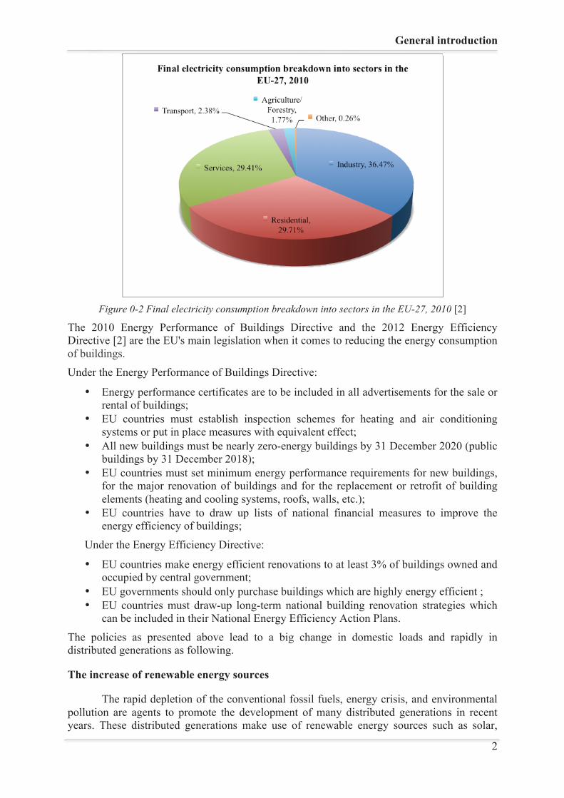
Energy consumption in buildings is divided into two categories, residential buildings and service buildings (or tertiary buildings). According to the report of ODYSSEE-MURE [1], buildings account for about 40% of total final energy consumption and around 55% of electricity consumption in the European Union (EU) in 2012. Buildings are the largest end-use sector with around two-thirds of the buildings consumptions for residential and one-third left for service as shown in Figure 0-1 and Figure 0-2. Reducing demand through the improved efficiency of devices and procedures in buildings would get a great benefit not only in the economy but also in ensuring stable energy future. By improving the energy efficiency of buildings, we could reduce total EU energy consumption by 5% to 6% and lower CO2 emission by about 5%.
Figure 0-1 Final energy consumption breakdown into sectors in the EU-27, 2010 [2]
The electricity intensity is clearly increasing in most countries in services, because of the growing number of new appliances, such as IT devices, linked to the development of the internet and of new telecommunication types, as well as a spread of air conditioning. At the EU level, the increase of electricity consumption in services between 2008 and 2012 is mainly due to structural changes, and to a lesser extent, to increase comfort and productivity increases due to the diffusion of ICT and air conditioning.
Policies to promote energy efficiency
Energy efficiency and renewable energy entail multiple benefits beyond energy savings and CO2 emission reductions. In recent years, EU countries have many policies to promote energy efficiency and renewable energy.
General introduction
2 2
Figure 0-2 Final electricity consumption breakdown into sectors in the EU-27, 2010 [2]
The 2010 Energy Performance of Buildings Directive and the 2012 Energy Efficiency Directive [2] are the EU's main legislation when it comes to reducing the energy consumption of buildings. Under the Energy Performance of Buildings Directive:
• Energy performance certificates are to be included in all advertisements for the sale or rental of buildings;
• EU countries must establish inspection schemes for heating and air conditioning systems or put in place measures with equivalent effect;
• All new buildings must be nearly zero-energy buildings by 31 December 2020 (public buildings by 31 December 2018);
• EU countries must set minimum energy performance requirements for new buildings, for the major renovation of buildings and for the replacement or retrofit of building elements (heating and cooling systems, roofs, walls, etc.);
• EU countries have to draw up lists of national financial measures to improve the energy efficiency of buildings;
Under the Energy Efficiency Directive:
• EU countries make energy efficient renovations to at least 3% of buildings owned and occupied by central government;
• EU governments should only purchase buildings which are highly energy efficient ; • EU countries must draw-up long-term national building renovation strategies which
can be included in their National Energy Efficiency Action Plans.
The policies as presented above lead to a big change in domestic loads and rapidly in distributed generations as following.
The increase of renewable energy sources
The rapid depletion of the conventional fossil fuels, energy crisis, and environmental pollution are agents to promote the development of many distributed generations in recent years. These distributed generations make use of renewable energy sources such as solar,

General introduction
3 3
wind, biomass, fuel cells etc. to generate electricity or heat. The cost of renewable energy technologies is on a falling trend and is expected to reduce further as demand and production increases, and becomes competitive with classical generations. Almost renewable energy generators are intrinsically DC sources, for example, photovoltaic panels (PVs), small wind turbines or fuel cells. Therefore DC-AC inverters are used to in order to integrate these generators into the power system. These renewable energy sources could replace the using of fossil fuels as oil and coal, reduce the CO2 emissions, ensure security energy and sustainable development.
The development of DC Loads
The DC loads are growing rapidly nowadays. The policies to promote energy efficiency, typically low-energy buildings and zero-energy buildings, of many countries in the world are the first reason [3]. The second, many works have shown the fact that new DC loads have energy efficient higher than AC loads and most of the tertiary building electric loads could be fed directly with DC power [4]. DC appliances include communication technologies and all consumer electronics, such as computers, telephones, televisions, compact fluorescent lighting with electronic ballasts, light-emitting diodes (LEDs), and efficient DC motors. Fluorescent and LED lighting uses one-quarter of the power consumption, or less than the traditional incandescent lighting. It is replacing in the residential and commercial sectors. Brushless DC permanent magnet motors can save 5-15% of the energy used by traditional AC induction motors, and up to 30-50% in variable-speed applications for pumping, ventilation, refrigeration, and space cooling. DC-motor-driven heat pump technologies for water and space heating can also displace conventional resistance heating with a savings of 50% or more. In addition to DC-internal appliances, electric vehicles (EVs) and plug-in hybrid electric vehicles (PHEVs) are expected to constitute a rapidly growing pure DC load in the foreseeable future.
Why a DC microgrid?
Currently, most of available architectures for electrical energy distribution are mainly centralized with AC topologies due to the fact that simple AC transformers can step up and down voltages to facilitate power system. The DC grid mainly applies for high-voltage transmission system to transport electricity in a very long distance. In low voltage system, DC only exists in ships, aircrafts, or railway applications. However, the significant change in both domestic loads, and renewable energy sources make the electrical manager consider DC as a viable alternative to improve energy efficiency and reliability of the electric system. In addition, the advances in power electronic technology recently make DC distribution become more attractive than AC system. The first reason is challenges the operating of the electric power system. The intermittent and unpredictable nature of renewable energy sources, such as wind turbine and photovoltaic, remains an issue for their integration into the public grid resulting in fluctuations of voltage and/or frequency, harmonic pollution, difficult in load management. The second, in traditional AC power system, PV generators produce DC power that is converted to AC to supply electric power system; then, this power has to be inverted to DC for many end users as mentioned above. This requires multi-stage DC-AC and AC-DC conversions, causing great amount of power losses, due to the AC reactive power consumption, and the converter losses. In order to increase the integration level of renewable energies and energy efficiency, the DC microgrid is proposed. The main difference of the microgrid from a conventional power generation is that the power generators are usually small and they are distributed and located in close proximity to the energy users. The major advantages of a DC microgrid in comparison with AC grid are:
General introduction
4 4
• DC grid maximizes the energy efficiency by avoiding multi-state converters and reducing conversion losses by using DC-DC converters.
• DC grid is simple in integrating with renewable energy sources without regard to matching phases, only voltage needs to be stable.
• DC grid is easy in coupling with electricity storage systems like batteries, super-capacitorsn, and DC load.
The DC microgrid can be applied in various fields, for example, commercial and office buildings, smart homes, data centers, shipboards, and aircraft, etc.
Motivations
While many research concentrates on the control strategies and energy management in the DC microgrids [5]–[8]the protection issue receives inadequate attention and lack of regulations and experiences. Protection in DC grids is more difficult than that in AC grid due to the continuous arc, higher short circuit current value and fault rate of rising. Furthermore, the DC distributed grids are composed of many electronic and semiconductor switching devices, which should withstand the overcurrent from 3 to 5 times rated values in some microseconds. In order to ensure the safety of these systems, the protection devices have to interrupt the faults in a very short time (some tens of microseconds). Mechanical circuit breakers, which have a response time in tens of milliseconds, seem not to meet the safety requirements of DC microgrid. The lack of efficient protection device is one of barriers to develop DC microgrid in the distributed system. Recent studies have indicated that solid-state DC circuit breaker (SSCB), which uses semiconductor device as main switch instead of mechanical switch, offers a great protection device for DC microgrid due to its fast response time can solve this problem.
Research objectives and approach
Link with the ANR C3μ project
Ampere Laboratory cooperates with “Laboratoire de Conception et d'Intégration des Systèmes” (LCIS) carry out an ANR (The French National Research Agency) C3μ project in order to develop a meshed DC microgrid. There exist numerous recommendations at the European or the National levels to improve the energy efficiency particularly in housings and buildings. DC microgrid or LVDC (Low Voltage Direct Current) was proposed some years ago for housing and office buildings to take advantage of the PV local production. Such smart grids increase the efficiency of the PV to user power chain due to the elimination of inverters and PFCs (Power Factor Corrector) needed in a classical AC-grid. Although most studies in the microgrids topic concern AC-grid because of the industrial standards, most of the modern office and housing equipment are DC loads or have DC voltage level, such as LED lightings, office automation devices, data centers, electric vehicle plugs, building elevators and the like. Power-line communication (including the high-speed Internet) is fully compatible with LVDC if twisted pairs of DC lines are used. However, most studies on DC-grid only concern point-to-point DC links. The meshed DC grid raises some problems to be investigated: voltage control, power flow control and stability of the grid. These meshed DC grids have rarely been investigated until now. A meshed DC grid may include loops. Nevertheless, the loops may be useful for controlling the power flows, enabling redundancy or simplifying the sizing. If such issues are difficult to be studied in super-grid and distribution grids, because of the cost of such demonstrators, they are much easier to test them on a DC microgrid. It includes a connection to the AC-grid with a circuit breaker, which may be a DC breaker or a standard AC breaker if placed between the

General introduction
5 5
AC-grid and the inverter. The DC circuit breaker may be smart and used as the interface for the communication between the microgrid and the AC-grid. The AC-DC inverter is bi-directional, it serves to both rectify (AC-DC) power from the grid to the building distribution system and invert (DC-AC) excess power from the DC sources to the AC grid. The DC microgrid may include one or more energy sources like solar cells, batteries or generators. DC-DC devices that receive power directly from the photovoltaic arrays or other sources convert them to the DC voltage bus (400 V DC). Furthermore, the grid includes an Electric Vehicle (EV) plugged into the grid, which yields possible redundancy that may be studied by a breaker for fault emulations (break emulator). Some energy storages (batteries or super-capacitors) may also be included because of the interest in smoothing the PV generation. Finally, smart switches may control the LED lightings by sending signals into the grid. Few studies concern a decentralized control of the grid, even if such concept leads to very robust systems. Some issues also concerning the DC bus itself impact the efficiency, particularly at the life-cycle assessment level, because of the need for copper. The smart plugs and DC breakers have to manage the security of the connection in case of faults. Finally, such new DC microgrids represent a clear advantage in term of efficiency with respect to AC-grid. However numerous scientific issues have to be studied as listed above. The topic represents an advance research area and fits very well within the ANR Call. As the electrical wiring is not similar to classical network architectures (bus, star or ring-shaped) but has a free topology, we will analyze the data exchanges suitable to meet the criteria for robust control and supervision both at the system and component levels. Nonetheless, to provide consistent IP network interfaces we propose to specify the 6LoWPAN protocol that provides robust control with a reduced bandwidth (COAP) and routing (RPL) regardless the network topology on AC and DC power line and already validated in the wireless use cases. The use of a DC plug with communication capacity as the unit element of the power network will allow an efficient management of the power and a more accurate measurement and dispatch of the energy flow.
The aim of the C3μ project is to build a benchmark platform of a meshed DC microgrid for delivery of electrical energy in the interior of the buildings for tertiary, commercial or residential buildings, with a decentralized management system to distribute needs and to associate in the most efficient way intermittent renewable sources of energy. The project is investigating the energy-saving potential, benefits, barriers, and safety of using DC microgrid to use local renewable energy systems directly in their DC forms, rather than converting them to AC currents and finally used in DC loads. The project is composed of 5 tasks: • Design and realization of elementary DC power management components;
• Consumption measure, transmission and data processing for exchange; • Development the platform to estimate gains of DC microgrid solution;
• Design of protocol and communication electronics for the grid; • Modeling energy management and reliability of the DC grid; this will be performed by building a Matlab/Simulink platform in order to simulate the meshed DC microgrid.
Research Objectives and Thesis Outline
My work under the sponsor of Glink project Erasmus Mundus program is connected to the ANR C3μ project but concentrates on the protection in DC microgrid issue. The objectives of the thesis are composed of two main parts. The first is to propose a DC circuit breaker, which will be used to protect for a meshed DC microgrid from short circuit current. The second goal is to build a mathematical model of the JFET in order to simulate the operation of proposed

General introduction
6 6
DC circuit breaker in Matlab/Simulink environment, which will be used in the simulation platform of the ANR C3μ project. The thesis is divided into 3 main chapters as follows:
In chapter 1, the protection in DC microgrid in literature will be reviewed. The features of the short circuit in DC microgrid are analyzed in order to indicate the requirements for protection devices. Then short circuit detection methods and solid state DC circuit breaker topologies are evaluated to select the most suitable method for the DC circuit breaker application. At the last of this chapter, the thesis will compare semiconductor devices, which can be used as main switches in the DC circuit breakers (IGBTs, MOSFETs, JFETs), in on-state losses and robustness with the short circuit. The failure modes of semiconductor switches are also mentioned here. These analyses allow us to select the SiC JFET device as the most suitable for fast and robust DC breaker solution. In chapter 2, characteristics of a commercial normally-on SiC JFET are investigated. Effectively, the mathematical model approaches are based on the electrical parameters of the semiconductor topology. To extract these parameters, static and dynamic measurements are implemented to select the rated parameters for the DC breaker. The tests with the JFET in short circuit and avalanche modes will be also performed; and the critical energy in each case will be calculated. Chapter 3 will propose an original DC circuit breaker configuration, which can automatically break/interrupt when a short circuit occurs in a very fast time. The operation of protection driver, which is composed of a voltage sensor and a forward-flyback converter, is described clearly in this chapter. The requirement on safety and reliability in operation will be also considered during the design process. The simulations of the original SiC JFET model in Matlab Simulink environment will be carried out in order to investigate the behaviors of the DC circuit breaker when it operates to protect the DC grid again overcurrent faults. Then the selection of devices of protection driver will be described in detail. Lastly, the validation tests are performed to verify proposed principle of the solid state DC circuit breaker.
Finally, conclusions and perspectives are given.
Chapter 1: State of the art in DC microgrid protection
7 7
CHAPTER 1: STATE OF THE ART IN DC MICROGRID PROTECTION
1.1 Introduction
This chapter presents a brief overview of the protection in the DC microgrid. In the first part, the basic concept of a DC microgrid is defined; and main components, some typical topologies, and applications are also introduced. The functions of protection devices and locations they should be placed in each type of configurations are discussed. Then, the chapter addresses types of short circuit and the comparison between the short circuit in the DC system and that in AC system. Due to the fact that there is no zero current crossing, an arc that appears upon breaking DC current cannot be extinguished naturally, making the protection of DC microgrid a difficult problem. This challenge results in harder requirements for DC circuit breakers in comparison with the case of AC.
The main part of the chapter is devoted to describing solid state DC circuit breaker technology. The application of power semiconductor devices to overcome the limitations of the conventional mechanical circuit breaker is discussed. The comparisons among other kinds of available semiconductor devices are carried out in order to select the most appropriate switching device for the circuit breaker application. The reliability of the DC circuit breaker will be discussed in the failure modes of the system.
1.2 Short circuit and protection in DC microgrids
1.2.1 Concept and structures of DC microgrids
DC microgrids were originally introduced in 2004 through the work of Ito et al, which illustrated the simpler control, superior efficiency, and reliability in comparison with its AC counterpart [9]. Accompanied by improvements in semiconductor materials and advancements in power electronics technology, DC systems can be flexible usage for diversity fields. They are becoming an increasingly popular solution for many types of residential and industrial applications such as telecom systems [10], distributed renewable and storage plants [11], data centers [12], residential households and buildings [13]–[17], fast EV charging stations [18], [19], and hybrid energy storage system [20]. A DC microgrid can be defined as a modern distributed power system in which differently alternative renewable energy sources, energy storage systems, and DC or AC loads are connected to a common DC bus either directly or through power electronics converters [21], [22]. It can be operated in an isolated configuration without the presence of utility grid, as shown in Figure 1-1; or it can also be integrated with the AC grid by using a DC-AC inverter. The inverter is used to transfer surplus or shortage energy into the grid, as shown in Figure 1-2. DC-DC converters are usually used to link renewable energy sources such as PVs, fuel cells, or storage units with the DC bus in order to control the power balance and bus voltage. Depending on the type and capacity of loads, they can be directly fed by the DC bus, or through DC-DC converters in order to step down the voltage to lower levels those are suitable for the requirements of loads. It can be considered that the main components of a DC microgrid are: sources, converters, energy storage systems, and loads. The microgrid
Chapter 1: State of the art in DC microgrid protection
8 8
technology in general and DC microgrid technology in particular commonly represents three important goals of a society: reliability, sustainability, and economics (cost optimizing, efficiency) [23].
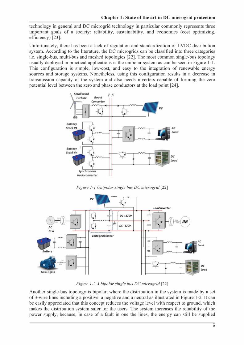
Unfortunately, there has been a lack of regulation and standardization of LVDC distribution system. According to the literature, the DC microgrids can be classified into three categories i.e. single-bus, multi-bus and meshed topologies [22]. The most common single-bus topology usually deployed in practical applications is the unipolar system as can be seen in Figure 1-1. This configuration is simple, low-cost, and easy to the integration of renewable energy sources and storage systems. Nonetheless, using this configuration results in a decrease in transmission capacity of the system and also needs inverters capable of forming the zero potential level between the zero and phase conductors at the load point [24].
Figure 1-1 Unipolar single bus DC microgrid [22]
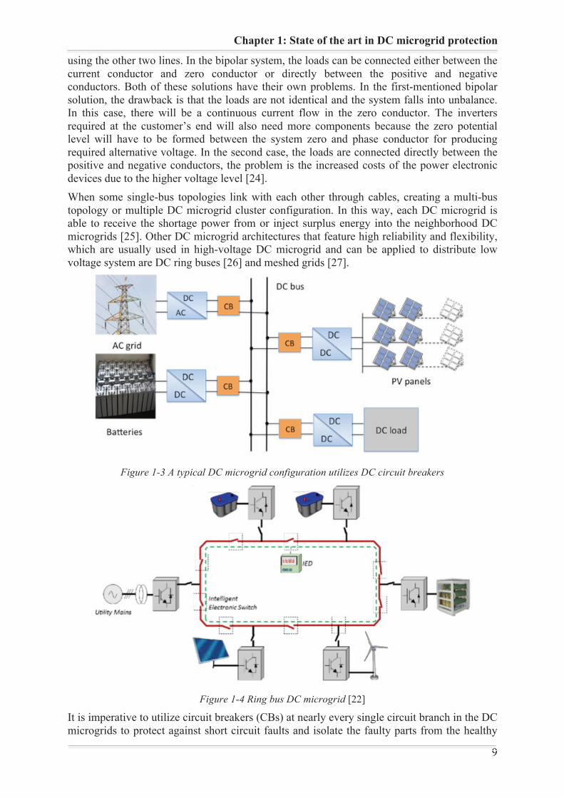
Figure 1-2 A bipolar single bus DC microgrid [22]
Another single-bus topology is bipolar, where the distribution in the system is made by a set of 3-wire lines including a positive, a negative and a neutral as illustrated in Figure 1-2. It can be easily appreciated that this concept reduces the voltage level with respect to ground, which makes the distribution system safer for the users. The system increases the reliability of the power supply, because, in case of a fault in one the lines, the energy can still be supplied
Chapter 1: State of the art in DC microgrid protection
9 9
using the other two lines. In the bipolar system, the loads can be connected either between the current conductor and zero conductor or directly between the positive and negative conductors. Both of these solutions have their own problems. In the first-mentioned bipolar solution, the drawback is that the loads are not identical and the system falls into unbalance. In this case, there will be a continuous current flow in the zero conductor. The inverters required at the customer’s end will also need more components because the zero potential level will have to be formed between the system zero and phase conductor for producing required alternative voltage. In the second case, the loads are connected directly between the positive and negative conductors, the problem is the increased costs of the power electronic devices due to the higher voltage level [24]. When some single-bus topologies link with each other through cables, creating a multi-bus topology or multiple DC microgrid cluster configuration. In this way, each DC microgrid is able to receive the shortage power from or inject surplus energy into the neighborhood DC microgrids [25]. Other DC microgrid architectures that feature high reliability and flexibility, which are usually used in high-voltage DC microgrid and can be applied to distribute low voltage system are DC ring buses [26] and meshed grids [27].
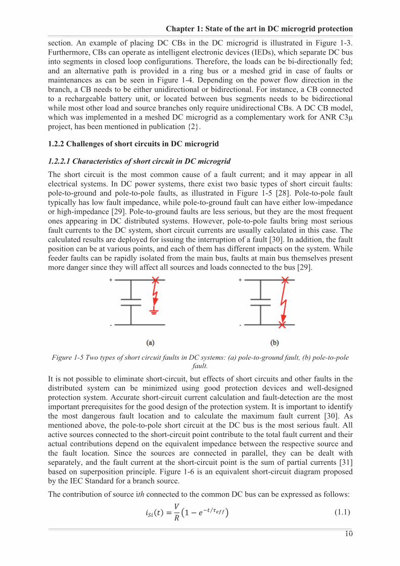
Figure 1-3 A typical DC microgrid configuration utilizes DC circuit breakers
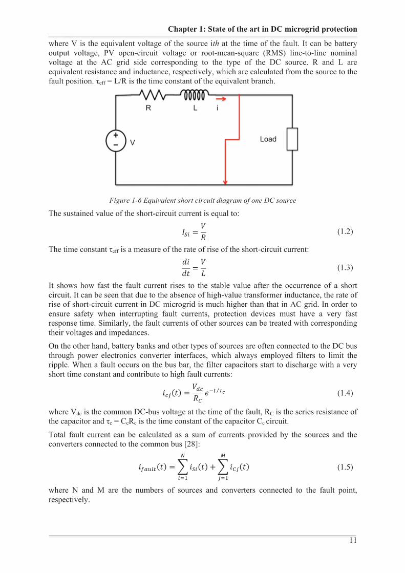
Figure 1-4 Ring bus DC microgrid [22]
It is imperative to utilize circuit breakers (CBs) at nearly every single circuit branch in the DC microgrids to protect against short circuit faults and isolate the faulty parts from the healthy
Chapter 1: State of the art in DC microgrid protection
10 10
section. An example of placing DC CBs in the DC microgrid is illustrated in Figure 1-3. Furthermore, CBs can operate as intelligent electronic devices (IEDs), which separate DC bus into segments in closed loop configurations. Therefore, the loads can be bi-directionally fed; and an alternative path is provided in a ring bus or a meshed grid in case of faults or maintenances as can be seen in Figure 1-4. Depending on the power flow direction in the branch, a CB needs to be either unidirectional or bidirectional. For instance, a CB connected to a rechargeable battery unit, or located between bus segments needs to be bidirectional while most other load and source branches only require unidirectional CBs. A DC CB model, which was implemented in a meshed DC microgrid as a complementary work for ANR C3μ project, has been mentioned in publication {2}.
1.2.2 Challenges of short circuits in DC microgrid
1.2.2.1 Characteristics of short circuit in DC microgrid The short circuit is the most common cause of a fault current; and it may appear in all electrical systems. In DC power systems, there exist two basic types of short circuit faults: pole-to-ground and pole-to-pole faults, as illustrated in Figure 1-5 [28]. Pole-to-pole fault typically has low fault impedance, while pole-to-ground fault can have either low-impedance or high-impedance [29]. Pole-to-ground faults are less serious, but they are the most frequent ones appearing in DC distributed systems. However, pole-to-pole faults bring most serious fault currents to the DC system, short circuit currents are usually calculated in this case. The calculated results are deployed for issuing the interruption of a fault [30]. In addition, the fault position can be at various points, and each of them has different impacts on the system. While feeder faults can be rapidly isolated from the main bus, faults at main bus themselves present more danger since they will affect all sources and loads connected to the bus [29].
Figure 1-5 Two types of short circuit faults in DC systems: (a) pole-to-ground fault, (b) pole-to-pole
fault.
It is not possible to eliminate short-circuit, but effects of short circuits and other faults in the distributed system can be minimized using good protection devices and well-designed protection system. Accurate short-circuit current calculation and fault-detection are the most important prerequisites for the good design of the protection system. It is important to identify the most dangerous fault location and to calculate the maximum fault current [30]. As mentioned above, the pole-to-pole short circuit at the DC bus is the most serious fault. All active sources connected to the short-circuit point contribute to the total fault current and their actual contributions depend on the equivalent impedance between the respective source and the fault location. Since the sources are connected in parallel, they can be dealt with separately, and the fault current at the short-circuit point is the sum of partial currents [31] based on superposition principle. Figure 1-6 is an equivalent short-circuit diagram proposed by the IEC Standard for a branch source.
The contribution of source ith connected to the common DC bus can be expressed as follows:
(1.1)
Chapter 1: State of the art in DC microgrid protection
11 11
where V is the equivalent voltage of the source ith at the time of the fault. It can be battery output voltage, PV open-circuit voltage or root-mean-square (RMS) line-to-line nominal voltage at the AC grid side corresponding to the type of the DC source. R and L are equivalent resistance and inductance, respectively, which are calculated from the source to the fault position. τeff = L/R is the time constant of the equivalent branch.
Figure 1-6 Equivalent short circuit diagram of one DC source
The sustained value of the short-circuit current is equal to:
(1.2)
The time constant τeff is a measure of the rate of rise of the short-circuit current:
(1.3)
It shows how fast the fault current rises to the stable value after the occurrence of a short circuit. It can be seen that due to the absence of high-value transformer inductance, the rate of rise of short-circuit current in DC microgrid is much higher than that in AC grid. In order to ensure safety when interrupting fault currents, protection devices must have a very fast response time. Similarly, the fault currents of other sources can be treated with corresponding their voltages and impedances. On the other hand, battery banks and other types of sources are often connected to the DC bus through power electronics converter interfaces, which always employed filters to limit the ripple. When a fault occurs on the bus bar, the filter capacitors start to discharge with a very short time constant and contribute to high fault currents:
(1.4)
where Vdc is the common DC-bus voltage at the time of the fault, RC is the series resistance of the capacitor and τc = CcRc is the time constant of the capacitor Cc circuit.
Total fault current can be calculated as a sum of currents provided by the sources and the converters connected to the common bus [28]:
(1.5)
where N and M are the numbers of sources and converters connected to the fault point, respectively.
Chapter 1: State of the art in DC microgrid protection
12 12
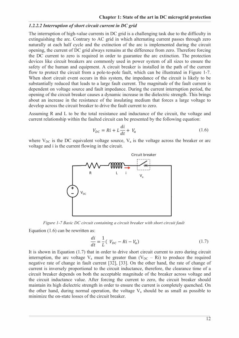
1.2.2.2 Interruption of short circuit current in DC grid
The interruption of high-value currents in DC grid is a challenging task due to the difficulty in extinguishing the arc. Contrary to AC grid in which alternating current passes through zero naturally at each half cycle and the extinction of the arc is implemented during the circuit opening, the current of DC grid always remains at the difference from zero. Therefore forcing the DC current to zero is required in order to guarantee the arc extinction. The protection devices like circuit breakers are commonly used in power system of all sizes to ensure the safety of the human and equipment. A circuit breaker is installed in the path of the current flow to protect the circuit from a pole-to-pole fault, which can be illustrated in Figure 1-7. When short circuit event occurs in this system, the impedance of the circuit is likely to be substantially reduced that leads to a large fault current. The magnitude of the fault current is dependent on voltage source and fault impedance. During the current interruption period, the opening of the circuit breaker causes a dynamic increase in the dielectric strength. This brings about an increase in the resistance of the insulating medium that forces a large voltage to develop across the circuit breaker to drive the fault current to zero.
Assuming R and L to be the total resistance and inductance of the circuit, the voltage and current relationship within the faulted circuit can be presented by the following equation:
(1.6)
where VDC is the DC equivalent voltage source, Va is the voltage across the breaker or arc voltage and i is the current flowing in the circuit.
Figure 1-7 Basic DC circuit containing a circuit breaker with short circuit fault
Equation (1.6) can be rewritten as:
(1.7)
It is shown in Equation (1.7) that in order to drive short circuit current to zero during circuit interruption, the arc voltage Va must be greater than (VDC – Ri) to produce the required negative rate of change in fault current [32], [33]. On the other hand, the rate of change of current is inversely proportional to the circuit inductance, therefore, the clearance time of a circuit breaker depends on both the acceptable magnitude of the breaker across voltage and the circuit inductance value. After forcing the current to zero, the circuit breaker should maintain its high dielectric strength in order to ensure the current is completely quenched. On the other hand, during normal operation, the voltage Va should be as small as possible to minimize the on-state losses of the circuit breaker.
Chapter 1: State of the art in DC microgrid protection
13 13
1.2.3 Requirements of a DC Circuit Breaker in the DC Microgrid
From above discussions, it can be seen that there are several requirements for every circuit breaker applying in the DC microgrid. Firstly a DC CB should have an ability of rapid tripping with adequate breaking capacity. As mentioned before, the DC microgrid heavily relies on power electronic sources, which have a limited fault current sustainability (typically 2-3 times of the nominal load current for tens of microseconds). Hence, the capacity of fast interruption fault current will prevent components and the system from destroying by overcurrent. Secondly, a DC CB should have high fault current limiting capacity in order to introduce a completed electrical insulator into the circuit to interrupt the short circuit current. Thirdly, it is able to dissipate the stored energy within the circuit inductance thus eliminating large voltage overshoots caused by sudden interruption of fault current. Lastly, it should have small on-state losses during normal operation. Notice that there is the trade-off between the first and the third aforementioned requirements with regard to the shorter response time, the higher rate of current change di/dt, or higher voltage spike the DC CB has. Therefore, it is necessary to obtain an optimizing response time, which satisfies both of requirements.
1.2.4 Comparison of protective devices technologies for DC grid
Currently, commercial protection devices available for low-voltage DC systems consist of fuses and mechanical circuit breakers [29]. However, they both introduce large response times, which cannot meet requirements of the protection in the DC microgrid. In addition, when they are used to interrupt the current, the appearance of the arc may lead to a dangerous condition in operation and CB contact erosion that results in reducing the lifetime and rising the maintenance costs. A fuse is composed of a fuse link and heat-absorbing material, which takes place inside a ceramic cartridge. It operates on the principle of melting down the fuse link to interrupt the overcurrent. Heat-absorbing material, which is usually silica sand is used to extinguish of the arc. Its ratings are given in RMS values of voltages and currents, which are available for both AC and DC systems. However, the interrupted current ability of the fuse depends on the time constant of the system. If the time constant is larger than certain limits, the fuse link will slowly melt and the temperature increases may prevent the heat-absorbing material to quench the arc [34]. A molded-case circuit breaker is composed of contactors, a quenching chamber, and a tripping device, which can be either thermal-magnetic or electronic. The multiple contactors are usually connected in series in order to guarantee sufficient blocking voltage rating. Substances, which have high insulation strength for example air, vacuum and sulfur hexafluoride (SF6), are introduced between the opened contacts to create the required insulator. The arc generated during the circuit interruption process helps to dissipate stored energy in the circuit inductance. The clearing fault times of classical circuit breakers are typically in the range of tens to hundreds of milliseconds (as shown in Figure 1-8), suitable for AC system. However, when they applied into systems that dominate by power electronic converters, the typical case is in DC microgrid, these interrupted speeds do not permit limiting fault currents before they can fully develop and do not provide substantial energy to the circuit inductance, leading dangers to the system. During the fault duration, filter capacitors within converters act as current sources and release a significant energy in a very short period of time. If the fault current does not interrupt on time, it may rise to a large value, which can cause further damages or unwanted trips of other protective devices [35]. A typical topology of a mechanical DC circuit breaker is displayed in Figure 1-9.
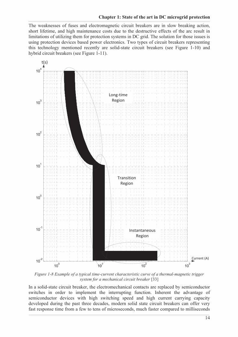
Chapter 1: State of the art in DC microgrid protection
14 14
The weaknesses of fuses and electromagnetic circuit breakers are in slow breaking action, short lifetime, and high maintenance costs due to the destructive effects of the arc result in limitations of utilizing them for protection systems in DC grid. The solution for those issues is using protection devices based power electronics. Two types of circuit breakers representing this technology mentioned recently are solid-state circuit breakers (see Figure 1-10) and hybrid circuit breakers (see Figure 1-11).
Figure 1-8 Example of a typical time-current characteristic curve of a thermal-magnetic trigger
system for a mechanical circuit breaker [33]
In a solid-state circuit breaker, the electromechanical contacts are replaced by semiconductor switches in order to implement the interrupting function. Inherent the advantage of semiconductor devices with high switching speed and high current carrying capacity developed during the past three decades, modern solid state circuit breakers can offer very fast response time from a few to tens of microseconds, much faster compared to milliseconds
100
101
102
103
10-2
10-1
100
101
102
103
104
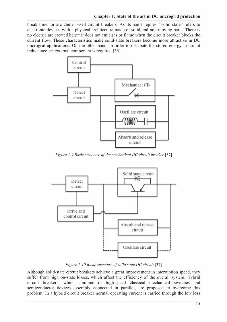
Chapter 1: State of the art in DC microgrid protection
15 15
break time for arc chute based circuit breakers. As its name replies, “solid state” refers to electronic devices with a physical architecture made of solid and non-moving parts. There is no electric arc created hence it does not emit gas or flame when the circuit breaker blocks the current flow. These characteristics make solid-state breakers become more attractive in DC microgrid applications. On the other hand, in order to dissipate the stored energy in circuit inductance, an external component is required [36].
Figure 1-9 Basic structure of the mechanical DC circuit breaker [37]
Figure 1-10 Basic structure of solid state DC circuit [37]
Although solid-state circuit breakers achieve a great improvement in interruption speed, they suffer from high on-state losses, which affect the efficiency of the overall system. Hybrid circuit breakers, which combine of high-speed classical mechanical switches and semiconductor devices assembly connected in parallel, are proposed to overcome this problem. In a hybrid circuit breaker normal operating current is carried through the low loss
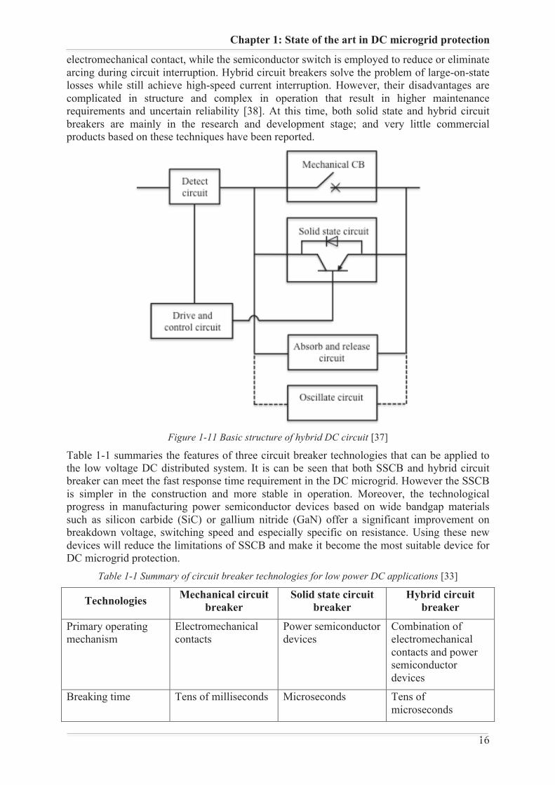
Chapter 1: State of the art in DC microgrid protection
16 16
electromechanical contact, while the semiconductor switch is employed to reduce or eliminate arcing during circuit interruption. Hybrid circuit breakers solve the problem of large-on-state losses while still achieve high-speed current interruption. However, their disadvantages are complicated in structure and complex in operation that result in higher maintenance requirements and uncertain reliability [38]. At this time, both solid state and hybrid circuit breakers are mainly in the research and development stage; and very little commercial products based on these techniques have been reported.
Figure 1-11 Basic structure of hybrid DC circuit [37]
Table 1-1 summaries the features of three circuit breaker technologies that can be applied to the low voltage DC distributed system. It is can be seen that both SSCB and hybrid circuit breaker can meet the fast response time requirement in the DC microgrid. However the SSCB is simpler in the construction and more stable in operation. Moreover, the technological progress in manufacturing power semiconductor devices based on wide bandgap materials such as silicon carbide (SiC) or gallium nitride (GaN) offer a significant improvement on breakdown voltage, switching speed and especially specific on resistance. Using these new devices will reduce the limitations of SSCB and make it become the most suitable device for DC microgrid protection.
Table 1-1 Summary of circuit breaker technologies for low power DC applications [33]
Technologies Mechanical circuit breaker
Solid state circuit breaker
Hybrid circuit breaker
Primary operating mechanism
Electromechanical contacts
Power semiconductor devices
Combination of electromechanical contacts and power semiconductor devices
Breaking time Tens of milliseconds Microseconds Tens of microseconds
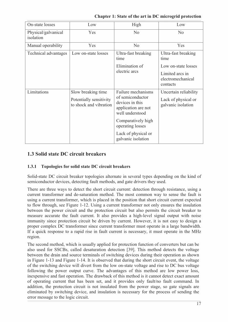
Chapter 1: State of the art in DC microgrid protection
17 17
On-state losses Low High Low
Physical/galvanical isolation
Yes No No
Manual operability Yes No Yes
Technical advantages Low on-state losses Ultra-fast breaking time
Elimination of electric arcs
Ultra-fast breaking time
Low on-state losses Limited arcs in electromechanical contacts
Limitations Slow breaking time Potentially sensitivity to shock and vibration
Failure mechanisms of semiconductor devices in this application are not well understoodComparatively high operating losses Lack of physical or galvanic isolation
Uncertain reliability Lack of physical or galvanic isolation
1.3 Solid state DC circuit breakers
1.3.1 Topologies for solid state DC circuit breakers
Solid-state DC circuit breaker topologies alternate in several types depending on the kind of semiconductor devices, detecting fault methods, and gate drivers they used.
There are three ways to detect the short circuit current: detection through resistance, using a current transformer and de-saturation method. The most common way to sense the fault is using a current transformer, which is placed in the position that short circuit current expected to flow through, see Figure 1-12. Using a current transformer not only ensures the insulation between the power circuit and the protection circuit but also permits the circuit breaker to measure accurate the fault current. It also provides a high-level signal output with noise immunity since protection circuit be driven by current. However, it is not easy to design a proper complex DC transformer since current transformer must operate in a large bandwidth. If a quick response to a rapid rise in fault current is necessary, it must operate in the MHz region.
The second method, which is usually applied for protection function of converters but can be also used for SSCBs, called desaturation detection [39]. This method detects the voltage between the drain and source terminals of switching devices during their operation as shown in Figure 1-13 and Figure 1-14. It is observed that during the short circuit event, the voltage of the switching device will divert from the low on-state voltage and rise to DC bus voltage following the power output curve. The advantages of this method are low power loss, inexpensive and fast operation. The drawback of this method is it cannot detect exact amount of operating current that has been set, and it provides only fault/no fault command. In addition, the protection circuit is not insulated from the power stage, so gate signals are eliminated by switching device, and insulation is necessary for the process of sending the error message to the logic circuit.
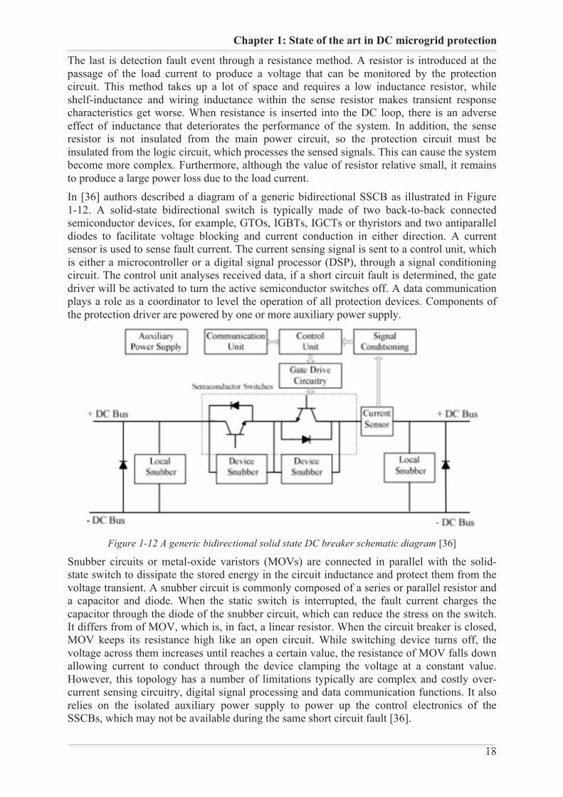
Chapter 1: State of the art in DC microgrid protection
18 18
The last is detection fault event through a resistance method. A resistor is introduced at the passage of the load current to produce a voltage that can be monitored by the protection circuit. This method takes up a lot of space and requires a low inductance resistor, while shelf-inductance and wiring inductance within the sense resistor makes transient response characteristics get worse. When resistance is inserted into the DC loop, there is an adverse effect of inductance that deteriorates the performance of the system. In addition, the sense resistor is not insulated from the main power circuit, so the protection circuit must be insulated from the logic circuit, which processes the sensed signals. This can cause the system become more complex. Furthermore, although the value of resistor relative small, it remains to produce a large power loss due to the load current. In [36] authors described a diagram of a generic bidirectional SSCB as illustrated in Figure 1-12. A solid-state bidirectional switch is typically made of two back-to-back connected semiconductor devices, for example, GTOs, IGBTs, IGCTs or thyristors and two antiparallel diodes to facilitate voltage blocking and current conduction in either direction. A current sensor is used to sense fault current. The current sensing signal is sent to a control unit, which is either a microcontroller or a digital signal processor (DSP), through a signal conditioning circuit. The control unit analyses received data, if a short circuit fault is determined, the gate driver will be activated to turn the active semiconductor switches off. A data communication plays a role as a coordinator to level the operation of all protection devices. Components of the protection driver are powered by one or more auxiliary power supply.
Figure 1-12 A generic bidirectional solid state DC breaker schematic diagram [36]
Snubber circuits or metal-oxide varistors (MOVs) are connected in parallel with the solid-state switch to dissipate the stored energy in the circuit inductance and protect them from the voltage transient. A snubber circuit is commonly composed of a series or parallel resistor and a capacitor and diode. When the static switch is interrupted, the fault current charges the capacitor through the diode of the snubber circuit, which can reduce the stress on the switch. It differs from of MOV, which is, in fact, a linear resistor. When the circuit breaker is closed, MOV keeps its resistance high like an open circuit. While switching device turns off, the voltage across them increases until reaches a certain value, the resistance of MOV falls down allowing current to conduct through the device clamping the voltage at a constant value. However, this topology has a number of limitations typically are complex and costly over-current sensing circuitry, digital signal processing and data communication functions. It also relies on the isolated auxiliary power supply to power up the control electronics of the SSCBs, which may not be available during the same short circuit fault [36].
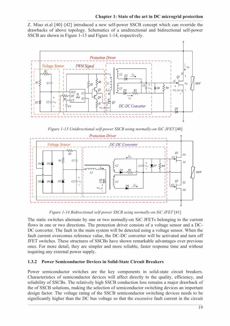
Chapter 1: State of the art in DC microgrid protection
19 19
Z. Miao et.al [40]–[42] introduced a new self-power SSCB concept which can override the drawbacks of above topology. Schematics of a unidirectional and bidirectional self-power SSCB are shown in Figure 1-13 and Figure 1-14, respectively.
Figure 1-13 Unidirectional self-power SSCB using normally-on SiC JFET [40]
Figure 1-14 Bidirectional self-power SSCB using normally-on SiC JFET [41]
The static switches alternate by one or two normally-on SiC JFETs belonging to the current flows in one or two directions. The protection driver consists of a voltage sensor and a DC-DC converter. The fault in the main system will be detected using a voltage sensor. When the fault current overcomes reference value, the DC-DC converter will be activated and turn off JFET switches. These structures of SSCBs have shown remarkable advantages over previous ones. For more detail, they are simpler and more reliable, faster response time and without requiring any external power supply.
1.3.2 Power Semiconductor Devices in Solid-State Circuit Breakers
Power semiconductor switches are the key components in solid-state circuit breakers. Characteristics of semiconductor devices will affect directly to the quality, efficiency, and reliability of SSCBs. The relatively high SSCB conduction loss remains a major drawback of the of SSCB solutions, making the selection of semiconductor switching devices an important design factor. The voltage rating of the SSCB semiconductor switching devices needs to be significantly higher than the DC bus voltage so that the excessive fault current in the circuit
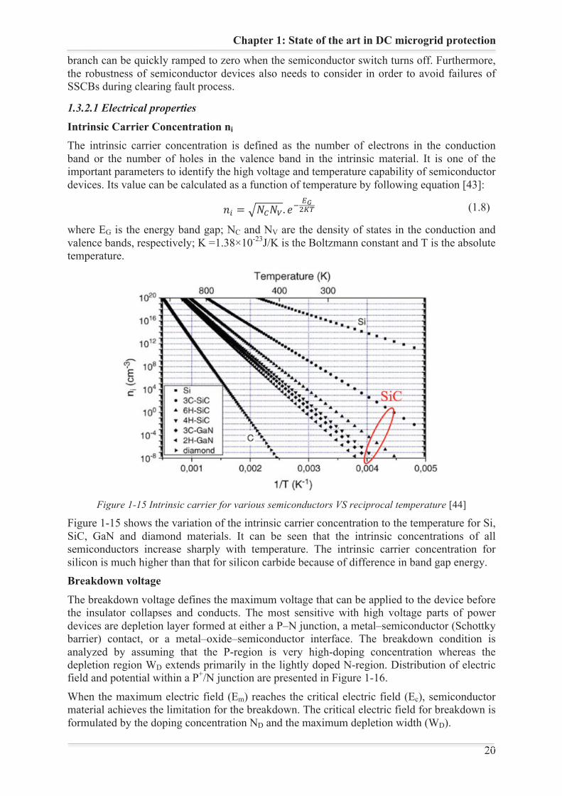
Chapter 1: State of the art in DC microgrid protection
20 20
branch can be quickly ramped to zero when the semiconductor switch turns off. Furthermore, the robustness of semiconductor devices also needs to consider in order to avoid failures of SSCBs during clearing fault process.
1.3.2.1 Electrical properties
Intrinsic Carrier Concentration ni The intrinsic carrier concentration is defined as the number of electrons in the conduction band or the number of holes in the valence band in the intrinsic material. It is one of the important parameters to identify the high voltage and temperature capability of semiconductor devices. Its value can be calculated as a function of temperature by following equation [43]:
(1.8)
where EG is the energy band gap; NC and NV are the density of states in the conduction and valence bands, respectively; K =1.38×10⁻²³J/K is the Boltzmann constant and T is the absolute temperature.
Figure 1-15 Intrinsic carrier for various semiconductors VS reciprocal temperature [44]
Figure 1-15 shows the variation of the intrinsic carrier concentration to the temperature for Si, SiC, GaN and diamond materials. It can be seen that the intrinsic concentrations of all semiconductors increase sharply with temperature. The intrinsic carrier concentration for silicon is much higher than that for silicon carbide because of difference in band gap energy. Breakdown voltage
The breakdown voltage defines the maximum voltage that can be applied to the device before the insulator collapses and conducts. The most sensitive with high voltage parts of power devices are depletion layer formed at either a P–N junction, a metal–semiconductor (Schottkybarrier) contact, or a metal–oxide–semiconductor interface. The breakdown condition is analyzed by assuming that the P-region is very high-doping concentration whereas the depletion region WD extends primarily in the lightly doped N-region. Distribution of electric field and potential within a P+/N junction are presented in Figure 1-16.
When the maximum electric field (Em) reaches the critical electric field (Ec), semiconductor material achieves the limitation for the breakdown. The critical electric field for breakdown is formulated by the doping concentration ND and the maximum depletion width (WD).
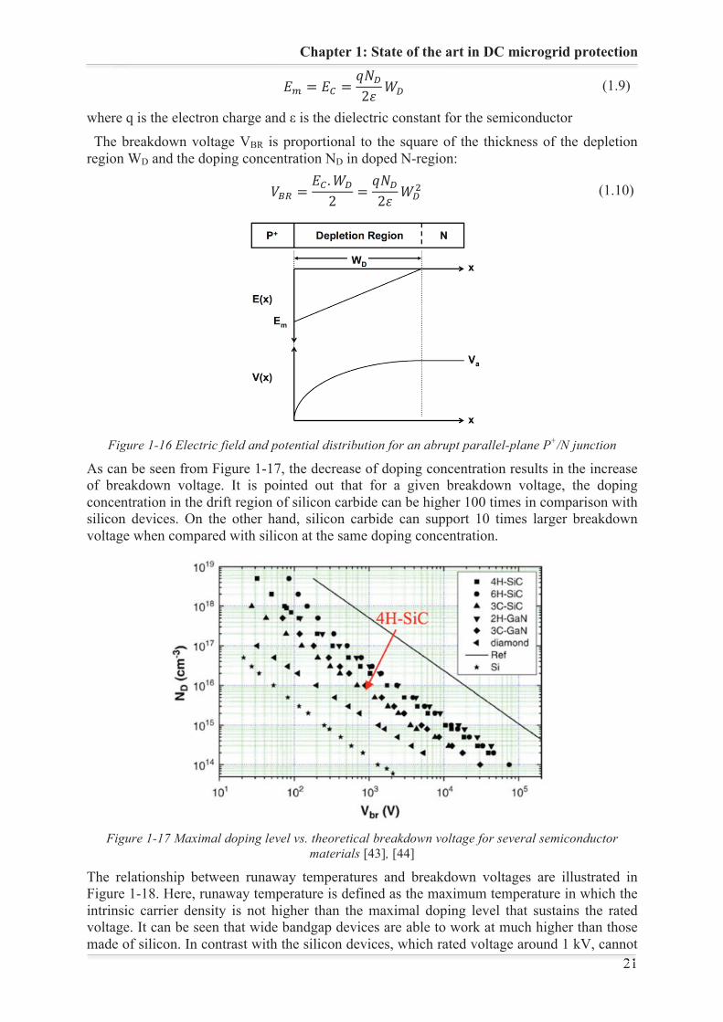
Chapter 1: State of the art in DC microgrid protection
21 21
(1.9)
where q is the electron charge and ε is the dielectric constant for the semiconductor The breakdown voltage VBR is proportional to the square of the thickness of the depletion region WD and the doping concentration ND in doped N-region:
(1.10)
Figure 1-16 Electric field and potential distribution for an abrupt parallel-plane P+/N junction
As can be seen from Figure 1-17, the decrease of doping concentration results in the increase of breakdown voltage. It is pointed out that for a given breakdown voltage, the doping concentration in the drift region of silicon carbide can be higher 100 times in comparison with silicon devices. On the other hand, silicon carbide can support 10 times larger breakdown voltage when compared with silicon at the same doping concentration.
Figure 1-17 Maximal doping level vs. theoretical breakdown voltage for several semiconductor materials [43], [44]
The relationship between runaway temperatures and breakdown voltages are illustrated in Figure 1-18. Here, runaway temperature is defined as the maximum temperature in which the intrinsic carrier density is not higher than the maximal doping level that sustains the rated voltage. It can be seen that wide bandgap devices are able to work at much higher than those made of silicon. In contrast with the silicon devices, which rated voltage around 1 kV, cannot
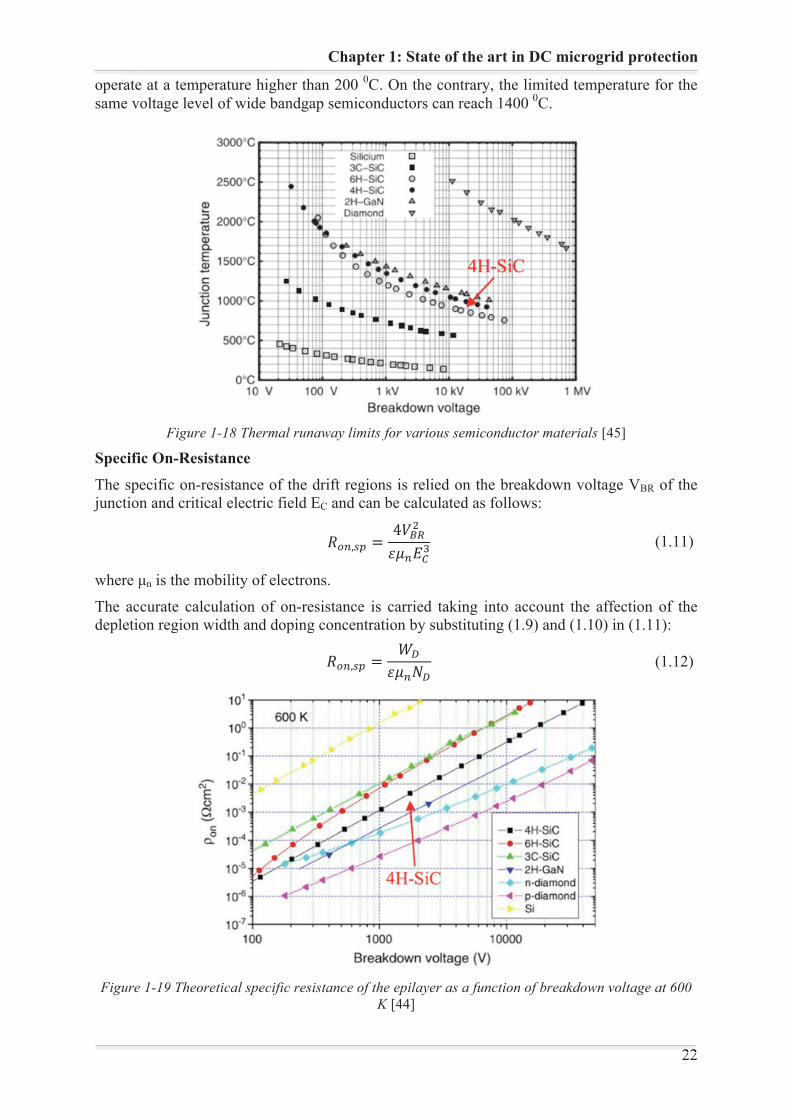
Chapter 1: State of the art in DC microgrid protection
22 22
operate at a temperature higher than 200 0C. On the contrary, the limited temperature for the same voltage level of wide bandgap semiconductors can reach 1400 0C.
Figure 1-18 Thermal runaway limits for various semiconductor materials [45]
Specific On-Resistance
The specific on-resistance of the drift regions is relied on the breakdown voltage VBR of the junction and critical electric field EC and can be calculated as follows:
(1.11)
where μn is the mobility of electrons.
The accurate calculation of on-resistance is carried taking into account the affection of the depletion region width and doping concentration by substituting (1.9) and (1.10) in (1.11):
(1.12)
Figure 1-19 Theoretical specific resistance of the epilayer as a function of breakdown voltage at 600
K [44]

Chapter 1: State of the art in DC microgrid protection
23 23
The Figure 1-19 shows the changes of the specific on-resistances to breakdown voltage for different semiconductor materials. We can see that the specific on-resistances increase accordance with the increase of breakdown voltage. The 4H-SiC devices have specific on-resistances smaller 1000 times than those of Si devices for the same voltage. Additional, with the same level of specific on-resistance, for example, 0.1 Ωcm2, the breakdown voltages of Si devices are limited to about 400 V while SiC devices permit these voltages beyond 2 kV.
1.3.2.2 Comparison of semiconductor materials
The physical properties of Si and several wide bandgap semiconductors such as SiC, GaN, and carbon (diamond) are summarized in Table 1 -2.
Table 1 -2 Physical properties of Si and major wide-bandgap semiconductors [45]
Property Si 4H-SiC GaN Diamond
Bandgap energy (eV) 1.12 3.20 3.39 5.45
Breakdown electric field (MV/cm2) 0.3 3.0 3.3 5.6
Thermal conductivity (W/cm.K) 1.3 4.9 1.3 20
Dielectric constant 11.7 10.0 9.5 5.5
Electron mobility (cm2/V.s) 1450 950 900 1900
Electron saturation velocity (cm/s) 106 2.7x10⁶ 2.5x10⁶ 2.7x10⁶
Wide bandgap semiconductor materials inherit superior electric and thermal characteristics in comparison. They promise a good alternative solution that can overcome the limitations of silicon in power semiconductor devices. A high critical electric field allows the design of power devices with smaller and higher-doped voltage-blocking regions and, as a result, a lower on-state resistance for a given breakdown voltage is achievable. The large bandgap leads to lower leakage currents than silicon, to a much higher operating temperature and higher radiation hardness. The high thermal conductivity permits dissipated heat to be more quickly extracted from the device avoiding the need to have bulky and expensive cooling systems in most applications. This reduces the cost in almost critical applications. Lastly, the saturated electron velocity of the wide bandgap device, which determines the maximum current density of the device, is twice that of silicon. Therefore, usage wide bandgap semiconductors replace silicon will allow improving the capability to block high voltage, provide low on-state drop and switch at high frequencies of converter and SSCB applications. However, except silicon technology, which is almost completed with very low-cost material and very high yield production, other materials are in the process of development. At present, GaN is available only as hetero-structures with a thin layer of GaN on top of other materials like sapphire, silicon or SiC. It is difficult to build vertical devices, thus making this material less interesting for power applications. Diamond technology is currently at the investigated stage, with no product available. In contrast, SiC has shown very good grown progress in recent years, with available commercial products from several manufacturers [46]. The structures of the available SiC power devices and their robustness are presented for SiC JFETs, MOSFETs and BJTs.
1.3.2.3 Structure of SiC devices
SiC JFETs The Junction Field Effect Transistor (JFET) is a voltage controlled device, in which there are not any PN junctions, alternating is a narrow piece of either P-type or N-type silicon carbide forming a “Channel” in order to majority carriers to flow through with two ohmic electrical
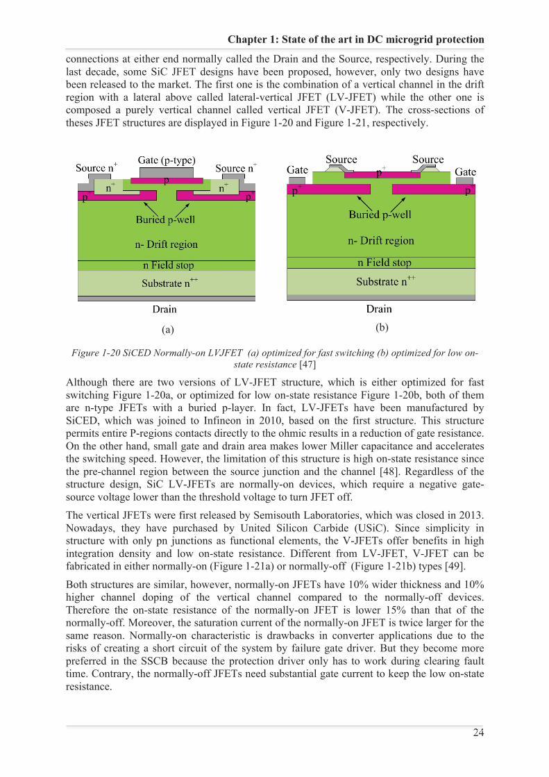
Chapter 1: State of the art in DC microgrid protection
24 24
connections at either end normally called the Drain and the Source, respectively. During the last decade, some SiC JFET designs have been proposed, however, only two designs have been released to the market. The first one is the combination of a vertical channel in the drift region with a lateral above called lateral-vertical JFET (LV-JFET) while the other one is composed a purely vertical channel called vertical JFET (V-JFET). The cross-sections of theses JFET structures are displayed in Figure 1-20 and Figure 1-21, respectively.
(a)
(b)
Figure 1-20 SiCED Normally-on LVJFET (a) optimized for fast switching (b) optimized for low on-state resistance [47]
Although there are two versions of LV-JFET structure, which is either optimized for fast switching Figure 1-20a, or optimized for low on-state resistance Figure 1-20b, both of them are n-type JFETs with a buried p-layer. In fact, LV-JFETs have been manufactured by SiCED, which was joined to Infineon in 2010, based on the first structure. This structure permits entire P-regions contacts directly to the ohmic results in a reduction of gate resistance. On the other hand, small gate and drain area makes lower Miller capacitance and accelerates the switching speed. However, the limitation of this structure is high on-state resistance since the pre-channel region between the source junction and the channel [48]. Regardless of the structure design, SiC LV-JFETs are normally-on devices, which require a negative gate-source voltage lower than the threshold voltage to turn JFET off. The vertical JFETs were first released by Semisouth Laboratories, which was closed in 2013. Nowadays, they have purchased by United Silicon Carbide (USiC). Since simplicity in structure with only pn junctions as functional elements, the V-JFETs offer benefits in high integration density and low on-state resistance. Different from LV-JFET, V-JFET can be fabricated in either normally-on (Figure 1-21a) or normally-off (Figure 1-21b) types [49].
Both structures are similar, however, normally-on JFETs have 10% wider thickness and 10% higher channel doping of the vertical channel compared to the normally-off devices. Therefore the on-state resistance of the normally-on JFET is lower 15% than that of the normally-off. Moreover, the saturation current of the normally-on JFET is twice larger for the same reason. Normally-on characteristic is drawbacks in converter applications due to the risks of creating a short circuit of the system by failure gate driver. But they become more preferred in the SSCB because the protection driver only has to work during clearing fault time. Contrary, the normally-off JFETs need substantial gate current to keep the low on-state resistance.
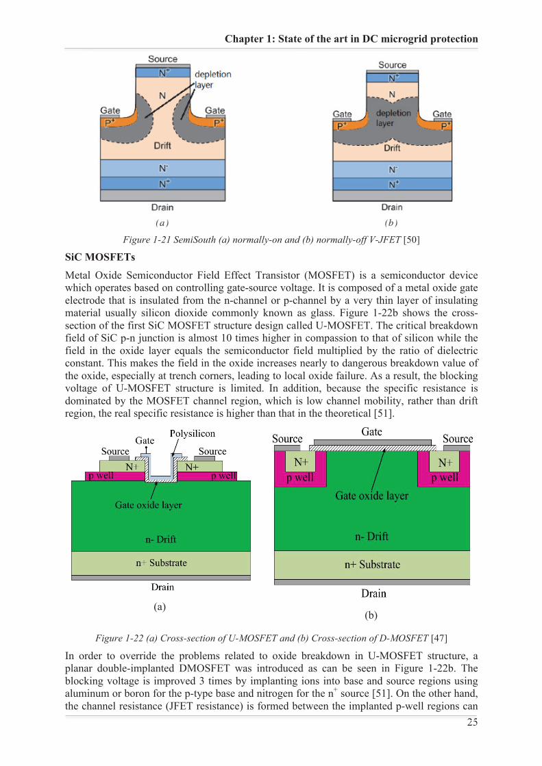
Chapter 1: State of the art in DC microgrid protection
25 25
Figure 1-21 SemiSouth (a) normally-on and (b) normally-off V-JFET [50]
SiC MOSFETs
Metal Oxide Semiconductor Field Effect Transistor (MOSFET) is a semiconductor device which operates based on controlling gate-source voltage. It is composed of a metal oxide gate electrode that is insulated from the n-channel or p-channel by a very thin layer of insulating material usually silicon dioxide commonly known as glass. Figure 1-22b shows the cross-section of the first SiC MOSFET structure design called U-MOSFET. The critical breakdown field of SiC p-n junction is almost 10 times higher in compassion to that of silicon while the field in the oxide layer equals the semiconductor field multiplied by the ratio of dielectric constant. This makes the field in the oxide increases nearly to dangerous breakdown value of the oxide, especially at trench corners, leading to local oxide failure. As a result, the blocking voltage of U-MOSFET structure is limited. In addition, because the specific resistance is dominated by the MOSFET channel region, which is low channel mobility, rather than drift region, the real specific resistance is higher than that in the theoretical [51].
(a)
(b)
Figure 1-22 (a) Cross-section of U-MOSFET and (b) Cross-section of D-MOSFET [47]
In order to override the problems related to oxide breakdown in U-MOSFET structure, a planar double-implanted DMOSFET was introduced as can be seen in Figure 1-22b. The blocking voltage is improved 3 times by implanting ions into base and source regions using aluminum or boron for the p-type base and nitrogen for the n+ source [51]. On the other hand, the channel resistance (JFET resistance) is formed between the implanted p-well regions can
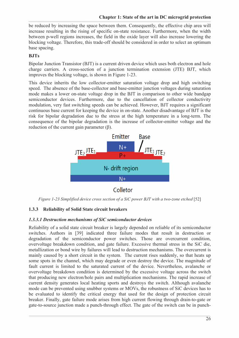
Chapter 1: State of the art in DC microgrid protection
26 26
be reduced by increasing the space between them. Consequently, the effective chip area will increase resulting in the rising of specific on-state resistance. Furthermore, when the width between p-well regions increases, the field in the oxide layer will also increase lowering the blocking voltage. Therefore, this trade-off should be considered in order to select an optimum base spacing.
BJTs Bipolar Junction Transistor (BJT) is a current driven device which uses both electron and hole charge carriers. A cross-section of a junction termination extension (JTE) BJT, which improves the blocking voltage, is shown in Figure 1-23.
This device inherits the low collector-emitter saturation voltage drop and high switching speed. The absence of the base-collector and base-emitter junction voltages during saturation mode makes a lower on-state voltage drop in the BJT in comparison to other wide bandgap semiconductor devices. Furthermore, due to the cancellation of collector conductivity modulation, very fast switching speeds can be achieved. However, BJT requires a significant continuous base current for keeping the device in on-state. Another disadvantage of BJT is the risk for bipolar degradation due to the stress at the high temperature in a long-term. The consequence of the bipolar degradation is the increase of collector-emitter voltage and the reduction of the current gain parameter (β).
Figure 1-23 Simplified device cross section of a SiC power BJT with a two-zone etched [52]
1.3.3 Reliability of Solid State circuit breakers
1.3.3.1 Destruction mechanisms of SiC semiconductor devices
Reliability of a solid state circuit breaker is largely depended on reliable of its semiconductor switches. Authors in [39] indicated three failure modes that result in destruction or degradation of the semiconductor power switches. Those are overcurrent condition, overvoltage breakdown condition, and gate failure. Excessive thermal stress in the SiC die, metallization or bond wire by failures will lead to destruction mechanisms. The overcurrent is mainly caused by a short circuit in the system. The current rises suddenly, so that heats up some spots in the channel, which may degrade or even destroy the device. The magnitude of fault current is limited to the saturated current of the device. Nevertheless, avalanche or overvoltage breakdown condition is determined by the excessive voltage across the switch that producing new electron/hole pairs and multiplication mechanisms. The rapid increase of current density generates local heating sports and destroys the switch. Although avalanche mode can be prevented using snubber systems or MOVs, the robustness of SiC devices has to be evaluated to identify the critical energy that used for the design of protection circuit breaker. Finally, gate failure mode arises from high current flowing through drain-to-gate or gate-to-source junction made a punch-through effect. The gate of the switch can be in punch-
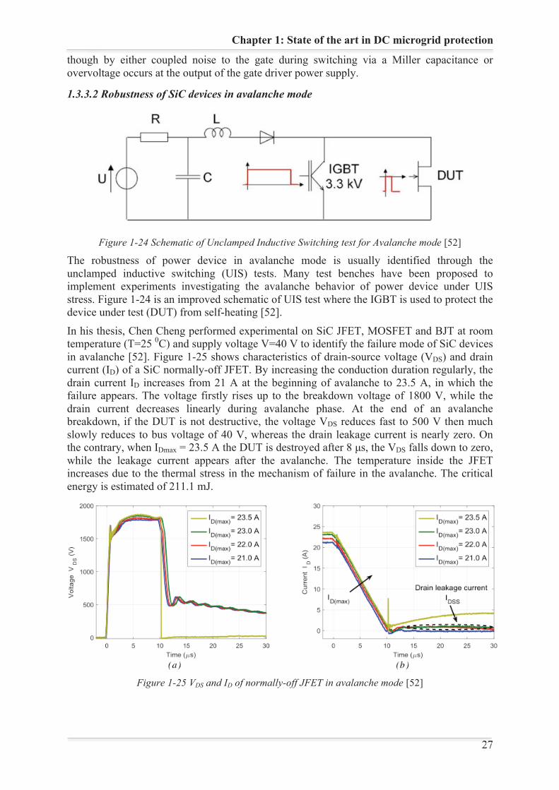
Chapter 1: State of the art in DC microgrid protection
27 27
though by either coupled noise to the gate during switching via a Miller capacitance or overvoltage occurs at the output of the gate driver power supply.
1.3.3.2 Robustness of SiC devices in avalanche mode
Figure 1-24 Schematic of Unclamped Inductive Switching test for Avalanche mode [52]
The robustness of power device in avalanche mode is usually identified through the unclamped inductive switching (UIS) tests. Many test benches have been proposed to implement experiments investigating the avalanche behavior of power device under UIS stress. Figure 1-24 is an improved schematic of UIS test where the IGBT is used to protect the device under test (DUT) from self-heating [52].
In his thesis, Chen Cheng performed experimental on SiC JFET, MOSFET and BJT at room temperature (T=25 0C) and supply voltage V=40 V to identify the failure mode of SiC devices in avalanche [52]. Figure 1-25 shows characteristics of drain-source voltage (VDS) and drain current (ID) of a SiC normally-off JFET. By increasing the conduction duration regularly, the drain current ID increases from 21 A at the beginning of avalanche to 23.5 A, in which the failure appears. The voltage firstly rises up to the breakdown voltage of 1800 V, while the drain current decreases linearly during avalanche phase. At the end of an avalanche breakdown, if the DUT is not destructive, the voltage VDS reduces fast to 500 V then much slowly reduces to bus voltage of 40 V, whereas the drain leakage current is nearly zero. On the contrary, when IDmax = 23.5 A the DUT is destroyed after 8 μs, the VDS falls down to zero, while the leakage current appears after the avalanche. The temperature inside the JFET increases due to the thermal stress in the mechanism of failure in the avalanche. The critical energy is estimated of 211.1 mJ.
Figure 1-25 VDS and ID of normally-off JFET in avalanche mode [52]
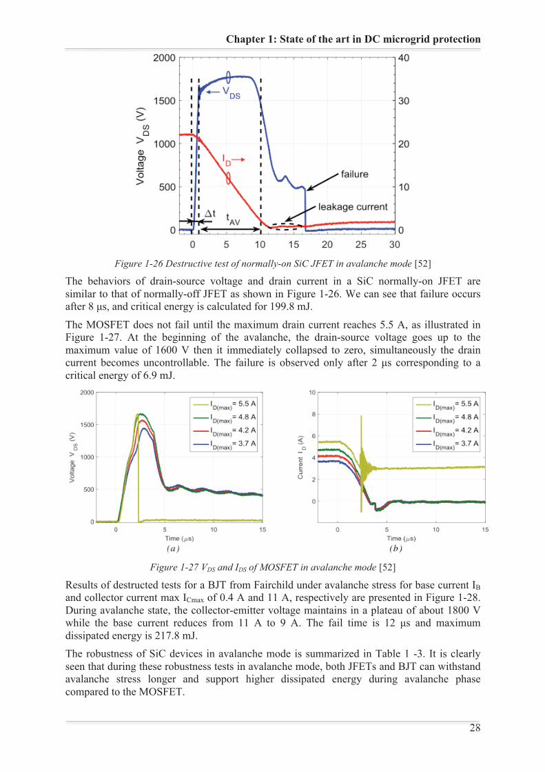
Chapter 1: State of the art in DC microgrid protection
28 28
Figure 1-26 Destructive test of normally-on SiC JFET in avalanche mode [52]
The behaviors of drain-source voltage and drain current in a SiC normally-on JFET are similar to that of normally-off JFET as shown in Figure 1-26. We can see that failure occurs after 8 μs, and critical energy is calculated for 199.8 mJ.
The MOSFET does not fail until the maximum drain current reaches 5.5 A, as illustrated in Figure 1-27. At the beginning of the avalanche, the drain-source voltage goes up to the maximum value of 1600 V then it immediately collapsed to zero, simultaneously the drain current becomes uncontrollable. The failure is observed only after 2 μs corresponding to a critical energy of 6.9 mJ.
Figure 1-27 VDS and IDS of MOSFET in avalanche mode [52]
Results of destructed tests for a BJT from Fairchild under avalanche stress for base current IBand collector current max ICmax of 0.4 A and 11 A, respectively are presented in Figure 1-28. During avalanche state, the collector-emitter voltage maintains in a plateau of about 1800 V while the base current reduces from 11 A to 9 A. The fail time is 12 μs and maximum dissipated energy is 217.8 mJ. The robustness of SiC devices in avalanche mode is summarized in Table 1 -3. It is clearly seen that during these robustness tests in avalanche mode, both JFETs and BJT can withstand avalanche stress longer and support higher dissipated energy during avalanche phase compared to the MOSFET.
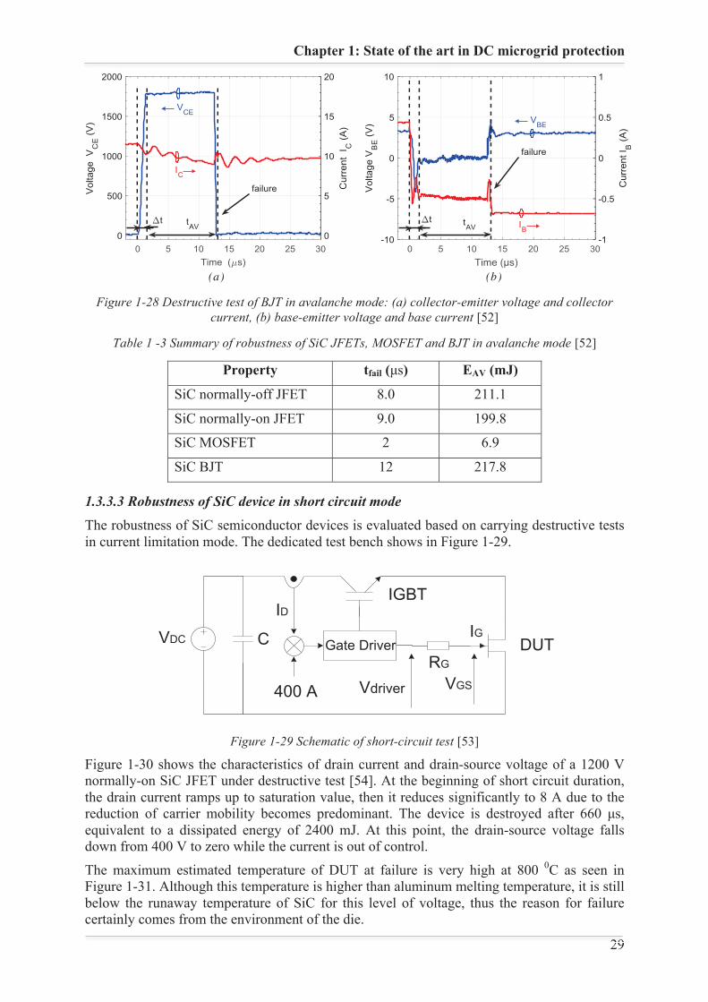
Chapter 1: State of the art in DC microgrid protection
29 29
Figure 1-28 Destructive test of BJT in avalanche mode: (a) collector-emitter voltage and collector
current, (b) base-emitter voltage and base current [52]
Table 1 -3 Summary of robustness of SiC JFETs, MOSFET and BJT in avalanche mode [52]
Property tfail (μs) EAV (mJ)
SiC normally-off JFET 8.0 211.1
SiC normally-on JFET 9.0 199.8
SiC MOSFET 2 6.9
SiC BJT 12 217.8
1.3.3.3 Robustness of SiC device in short circuit mode
The robustness of SiC semiconductor devices is evaluated based on carrying destructive tests in current limitation mode. The dedicated test bench shows in Figure 1-29.
Figure 1-29 Schematic of short-circuit test [53]
Figure 1-30 shows the characteristics of drain current and drain-source voltage of a 1200 V normally-on SiC JFET under destructive test [54]. At the beginning of short circuit duration, the drain current ramps up to saturation value, then it reduces significantly to 8 A due to the reduction of carrier mobility becomes predominant. The device is destroyed after 660 μs, equivalent to a dissipated energy of 2400 mJ. At this point, the drain-source voltage falls down from 400 V to zero while the current is out of control.
The maximum estimated temperature of DUT at failure is very high at 800 0C as seen in Figure 1-31. Although this temperature is higher than aluminum melting temperature, it is still below the runaway temperature of SiC for this level of voltage, thus the reason for failure certainly comes from the environment of the die.
(a) (b)
Gate DriverVDC
Vdriver VGS
IGDUT
RG
ID
400 A
C
IGBT
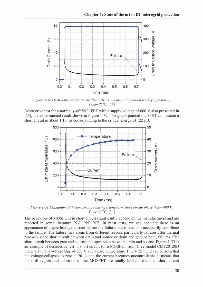
Chapter 1: State of the art in DC microgrid protection
30 30
Figure 1-30 Destructive test for normally-on JFET in current limitation mode (VDC=400 V,
TCASE=250C) [54]
Destructive test for a normally-off SiC JFET with a supply voltage of 600 V also presented in [55], the experimental result shows in Figure 1-32. The graph pointed out JFET can sustain a short circuit in about 1.17 ms corresponding to the critical energy of 122 mJ.
Figure 1-31 Estimation of the temperature during a long term short circuit phase (VDC=400 V,
TCASE=250C) [54]
The behaviors of MOSFETs in short circuit significantly depend on the manufacturers and are reported in some literature [53], [55]–[57]. In most tests, we can see that there is an appearance of a gate leakage current before the failure, but it does not necessarily contribute to the failure. The failure may come from different reasons particularly failures after thermal runaway since short circuit between drain and source or drain and gate or both; failures after short circuit between gate and source and open-state between drain and source. Figure 1-33 is an example of destructive test in short circuit for a MOSFET from Cree model CMF20120D under a DC bus voltage UDC of 600 V and a case temperature Tcase = 25 °C. It can be seen that the voltage collapses to zero at 20 μs and the current becomes uncontrollable. It means that the drift region and substrate of the MOSFET are totally broken results in short circuit
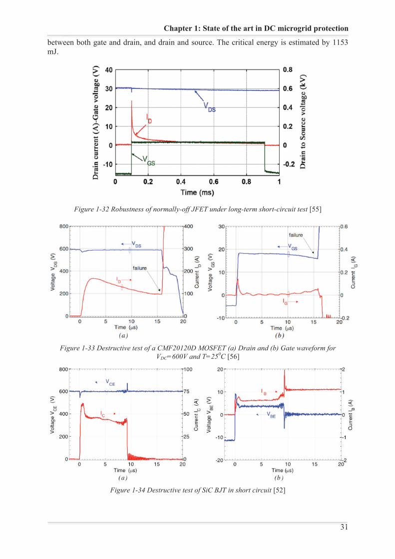
Chapter 1: State of the art in DC microgrid protection
31 31
between both gate and drain, and drain and source. The critical energy is estimated by 1153 mJ.
Figure 1-32 Robustness of normally-off JFET under long-term short-circuit test [55]
Figure 1-33 Destructive test of a CMF20120D MOSFET (a) Drain and (b) Gate waveform for
VDC=600V and T=250C [56]
Figure 1-34 Destructive test of SiC BJT in short circuit [52]
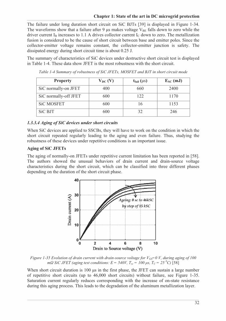
Chapter 1: State of the art in DC microgrid protection
32 32
The failure under long duration short circuit on SiC BJTs [39] is displayed in Figure 1-34. The waveforms show that a failure after 9 μs makes voltage VBE falls down to zero while the driver current IB increases to 1.1 A drives collector current IC down to zero. The metallization fusion is considered to be the cause of short circuit between base and emitter poles. Since the collector-emitter voltage remains constant, the collector-emitter junction is safety. The dissipated energy during short circuit time is about 0.25 J. The summary of characteristics of SiC devices under destructive short circuit test is displayed in Table 1-4. These data show JFET is the most robustness with the short circuit.
Table 1-4 Summary of robustness of SiC JFETs, MOSFET and BJT in short circuit mode
Property VDC (V) tfail (μs) ESC (mJ)
SiC normally-on JFET 400 660 2400
SiC normally-off JFET 600 122 1170
SiC MOSFET 600 16 1153
SiC BJT 600 32 246
1.3.3.4 Aging of SiC devices under short circuits
When SiC devices are applied to SSCBs, they will have to work on the condition in which the short circuit repeated regularly leading to the aging and even failure. Thus, studying the robustness of these devices under repetitive conditions is an important issue. Aging of SiC JFETs
The aging of normally-on JFETs under repetitive current limitation has been reported in [58]. The authors showed the unusual behaviors of drain current and drain-source voltage characteristics during the short circuit, which can be classified into three different phases depending on the duration of the short circuit phase.
Figure 1-35 Evolution of drain current with drain-source voltage for VGS=0 V, during aging of 100
mΩ SiC JFET (aging test conditions: E = 540V, Tsc = 100 μs, TC = 25 0C) [58]
When short circuit duration is 100 μs in the first phase, the JFET can sustain a large number of repetitive short circuits (up to 46,000 short circuits) without failure, see Figure 1-35. Saturation current regularly reduces corresponding with the increase of on-state resistance during this aging process. This leads to the degradation of the aluminum metallization layer.
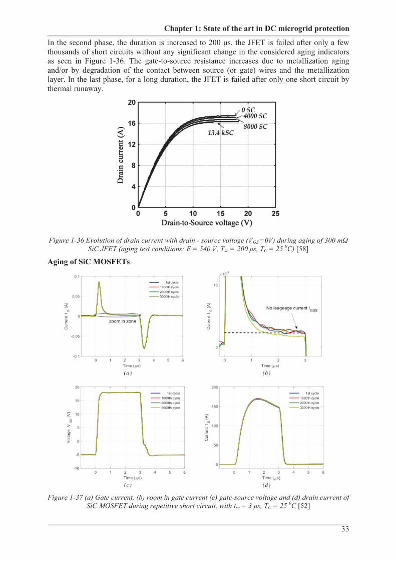
Chapter 1: State of the art in DC microgrid protection
33 33
In the second phase, the duration is increased to 200 μs, the JFET is failed after only a few thousands of short circuits without any significant change in the considered aging indicators as seen in Figure 1-36. The gate-to-source resistance increases due to metallization aging and/or by degradation of the contact between source (or gate) wires and the metallization layer. In the last phase, for a long duration, the JFET is failed after only one short circuit by thermal runaway.
Figure 1-36 Evolution of drain current with drain - source voltage (VGS =0V) during aging of 300 mΩ
SiC JFET (aging test conditions: E = 540 V, Tsc = 200 μs, TC = 25 0C) [58]
Aging of SiC MOSFETs
Figure 1-37 (a) Gate current, (b) room in gate current (c) gate-source voltage and (d) drain current of
SiC MOSFET during repetitive short circuit, with tsc = 3 μs, TC = 25 0C [52]
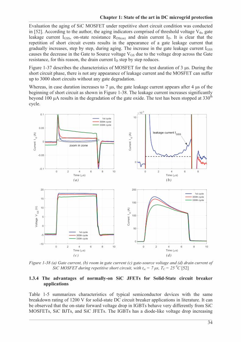
Chapter 1: State of the art in DC microgrid protection
34 34
Evaluation the aging of SiC MOSFET under repetitive short circuit condition was conducted in [52]. According to the author, the aging indicators comprised of threshold voltage Vth, gate leakage current IGSS, on-state resistance RDS(on) and drain current ID. It is clear that the repetition of short circuit events results in the appearance of a gate leakage current that gradually increases, step by step, during aging. The increase in the gate leakage current IGSS causes the decrease in the Gate to Source voltage VGS due to the voltage drop across the Gate resistance, for this reason, the drain current ID step by step reduces.
Figure 1-37 describes the characteristics of MOSFET for the test duration of 3 μs. During the short circuit phase, there is not any appearance of leakage current and the MOSFET can suffer up to 3000 short circuits without any gate degradation. Whereas, in case duration increases to 7 μs, the gate leakage current appears after 4 μs of the beginning of short circuit as shown in Figure 1-38. The leakage current increases significantly beyond 100 μA results in the degradation of the gate oxide. The test has been stopped at 330th cycle.
Figure 1-38 (a) Gate current, (b) room in gate current (c) gate-source voltage and (d) drain current of
SiC MOSFET during repetitive short circuit, with tsc = 7 μs, TC = 25 0C [52]
1.3.4 The advantages of normally-on SiC JFETs for Solid-State circuit breaker applications
Table 1-5 summarizes characteristics of typical semiconductor devices with the same breakdown rating of 1200 V for solid-state DC circuit breaker applications in literature. It can be observed that the on-state forward voltage drop in IGBTs behave very differently from SiC MOSFETs, SiC BJTs, and SiC JFETs. The IGBTs has a diode-like voltage drop increasing
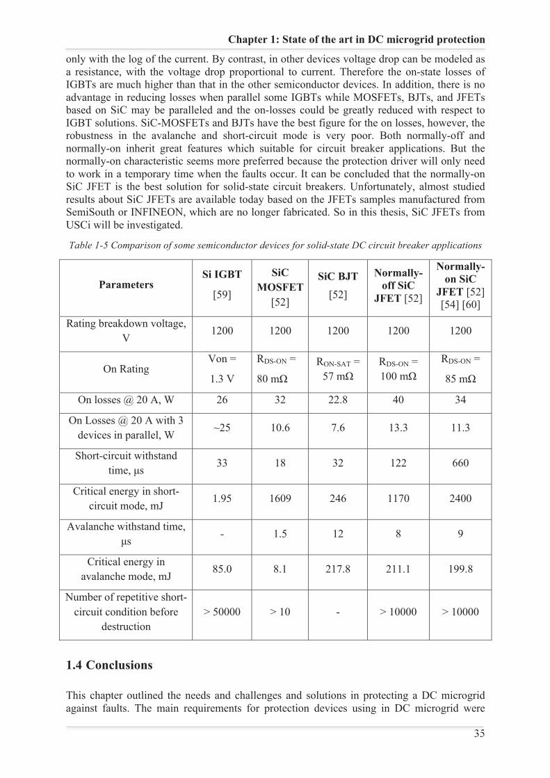
Chapter 1: State of the art in DC microgrid protection
35 35
only with the log of the current. By contrast, in other devices voltage drop can be modeled as a resistance, with the voltage drop proportional to current. Therefore the on-state losses of IGBTs are much higher than that in the other semiconductor devices. In addition, there is no advantage in reducing losses when parallel some IGBTs while MOSFETs, BJTs, and JFETs based on SiC may be paralleled and the on-losses could be greatly reduced with respect to IGBT solutions. SiC-MOSFETs and BJTs have the best figure for the on losses, however, the robustness in the avalanche and short-circuit mode is very poor. Both normally-off and normally-on inherit great features which suitable for circuit breaker applications. But the normally-on characteristic seems more preferred because the protection driver will only need to work in a temporary time when the faults occur. It can be concluded that the normally-on SiC JFET is the best solution for solid-state circuit breakers. Unfortunately, almost studied results about SiC JFETs are available today based on the JFETs samples manufactured from SemiSouth or INFINEON, which are no longer fabricated. So in this thesis, SiC JFETs from USCi will be investigated.
Table 1-5 Comparison of some semiconductor devices for solid-state DC circuit breaker applications
Parameters Si IGBT
[59]
SiC MOSFET
[52]
SiC BJT [52]
Normally-off SiC
JFET [52]
Normally-on SiC
JFET [52] [54] [60]
Rating breakdown voltage, V
1200 1200 1200 1200 1200
On Rating Von =
1.3 V
RDS-ON =
80 mΩ RON-SAT =
57 mΩ RDS-ON = 100 mΩ
RDS-ON =
85 mΩ
On losses @ 20 A, W 26 32 22.8 40 34
On Losses @ 20 A with 3 devices in parallel, W
~25 10.6 7.6 13.3 11.3
Short-circuit withstand time, μs
33 18 32 122 660
Critical energy in short-circuit mode, mJ
1.95 1609 246 1170 2400
Avalanche withstand time, μs
- 1.5 12 8 9
Critical energy in avalanche mode, mJ
85.0 8.1 217.8 211.1 199.8
Number of repetitive short-circuit condition before
destruction > 50000 > 10 - > 10000 > 10000
1.4 Conclusions
This chapter outlined the needs and challenges and solutions in protecting a DC microgrid against faults. The main requirements for protection devices using in DC microgrid were
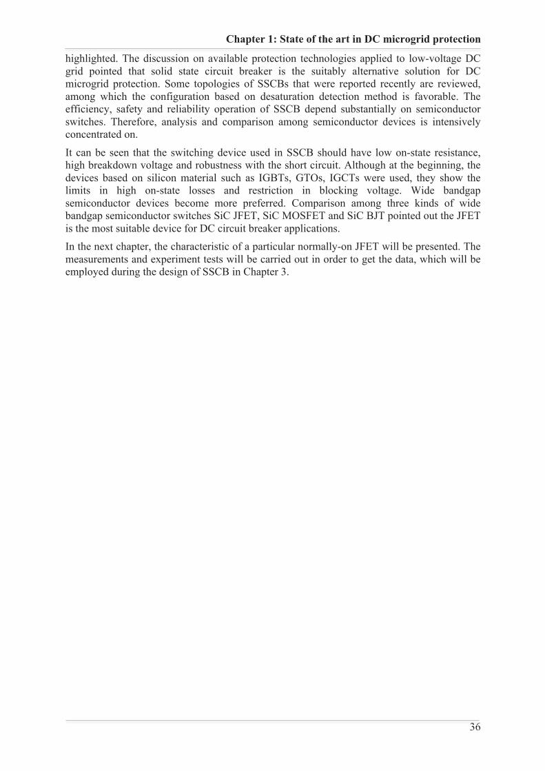
Chapter 1: State of the art in DC microgrid protection
36 36
highlighted. The discussion on available protection technologies applied to low-voltage DC grid pointed that solid state circuit breaker is the suitably alternative solution for DC microgrid protection. Some topologies of SSCBs that were reported recently are reviewed, among which the configuration based on desaturation detection method is favorable. The efficiency, safety and reliability operation of SSCB depend substantially on semiconductor switches. Therefore, analysis and comparison among semiconductor devices is intensively concentrated on.
It can be seen that the switching device used in SSCB should have low on-state resistance, high breakdown voltage and robustness with the short circuit. Although at the beginning, the devices based on silicon material such as IGBTs, GTOs, IGCTs were used, they show the limits in high on-state losses and restriction in blocking voltage. Wide bandgap semiconductor devices become more preferred. Comparison among three kinds of wide bandgap semiconductor switches SiC JFET, SiC MOSFET and SiC BJT pointed out the JFET is the most suitable device for DC circuit breaker applications. In the next chapter, the characteristic of a particular normally-on JFET will be presented. The measurements and experiment tests will be carried out in order to get the data, which will be employed during the design of SSCB in Chapter 3.
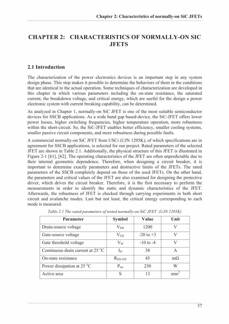
Chapter 2: Characteristics of normally-on SiC JFETs
37 37
CHAPTER 2: CHARACTERISTICS OF NORMALLY-ON SICJFETS
2.1 Introduction
The characterization of the power electronics devices is an important step in any system design phase. This step makes it possible to determine the behaviors of them in the conditions that are identical to the actual operation. Some techniques of characterization are developed in this chapter in which various parameters including the on-state resistance, the saturated current, the breakdown voltage, and critical energy, which are useful for the design a power electronic system with current breaking capability, can be determined.
As analyzed in Chapter 1, normally-on SiC JFET is one of the most suitable semiconductor devices for SSCB applications. As a wide band gap based-device, the SiC-JFET offers lower power losses, higher switching frequencies, higher temperature operation, more robustness within the short-circuit. So, the SiC-JFET enables better efficiency, smaller cooling systems, smaller passive circuit components, and more robustness during possible faults. A commercial normally-on SiC JFET from USCi (UJN 1205K), of which specifications are in agreement for SSCB applications, is selected for our project. Rated parameters of the selected JFET are shown in Table 2.1. Additionally, the physical structure of this JFET is illustrated in Figure 2-1 [61], [62]. The operating characteristics of the JFET are often unpredictable due to their internal geometric dependence. Therefore, when designing a circuit breaker, it is important to determine exactly parameters and destructive limits of the JFETs. The rated parameters of the SSCB completely depend on those of the used JFETs. On the other hand, the parameters and critical values of the JFET are also examined for designing the protective driver, which drives the circuit breaker. Therefore, it is the first necessary to perform the measurements in order to identify the static and dynamic characteristics of the JFET. Afterwards, the robustness of JFET is checked through carrying experiments in both short circuit and avalanche modes. Last but not least, the critical energy corresponding to each mode is measured.
Table 2.1 The rated parameters of tested normally-on SiC JFET (UJN 1205K)
Parameter Symbol Value Unit
Drain-source voltage VDS 1200 V
Gate-source voltage VGS -20 to +3 V
Gate threshold voltage Vt0 -10 to -4 V
Continuous drain current at 25 oC ID 38 A
On-state resistance RDS-ON 45 mΩ
Power dissipation at 25 oC Ptot 230 W
Active area S 13 mm2
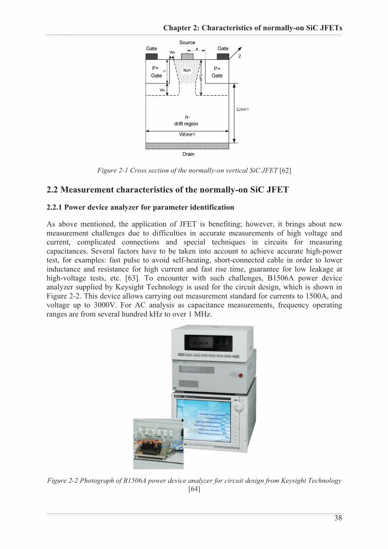
Chapter 2: Characteristics of normally-on SiC JFETs
38 38
Figure 2-1 Cross section of the normally-on vertical SiC JFET [62]
2.2 Measurement characteristics of the normally-on SiC JFET
2.2.1 Power device analyzer for parameter identification
As above mentioned, the application of JFET is benefiting; however, it brings about new measurement challenges due to difficulties in accurate measurements of high voltage and current, complicated connections and special techniques in circuits for measuring capacitances. Several factors have to be taken into account to achieve accurate high-power test, for examples: fast pulse to avoid self-heating, short-connected cable in order to lower inductance and resistance for high current and fast rise time, guarantee for low leakage at high-voltage tests, etc. [63]. To encounter with such challenges, B1506A power device analyzer supplied by Keysight Technology is used for the circuit design, which is shown in Figure 2-2. This device allows carrying out measurement standard for currents to 1500A, and voltage up to 3000V. For AC analysis as capacitance measurements, frequency operating ranges are from several hundred kHz to over 1 MHz.
Figure 2-2 Photograph of B1506A power device analyzer for circuit design from Keysight Technology
[64]
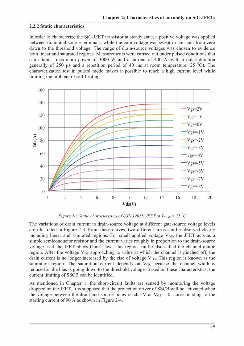
Chapter 2: Characteristics of normally-on SiC JFETs
39 39
2.2.2 Static characteristics
In order to characterize the SiC-JFET transistor at steady state, a positive voltage was applied between drain and source terminals, while the gate voltage was swept in constant from zero down to the threshold voltage. The range of drain-source voltages was chosen to evidence both linear and saturated regions. Measurements were carried out under pulsed conditions that can attain a maximum power of 3000 W and a current of 400 A, with a pulse duration generally of 250 μs and a repetition period of 40 ms at room temperature (25 0C). The characterization test in pulsed mode makes it possible to reach a high current level while limiting the problem of self-heating.
Figure 2-3 Static characteristics of UJN 1205K JFET at TCASE = 25 0C
The variations of drain current to drain-source voltage at different gate-source voltage levels are illustrated in Figure 2-3. From these curves, two different areas can be observed clearly including linear and saturated regions. For small applied voltage VDS, the JFET acts as a simple semiconductor resistor and the current varies roughly in proportion to the drain-source voltage as if the JFET obeys Ohm's law. This region can be also called the channel ohmic region. After the voltage VDS approaching to value at which the channel is pinched off, the drain current is no longer increased by the rise of voltage VDS. This region is known as the saturation region. The saturation current depends on VGS because the channel width is reduced as the bias is going down to the threshold voltage. Based on these characteristics, the current limiting of SSCB can be identified.
As mentioned in Chapter 1, the short-circuit faults are sensed by monitoring the voltage dropped on the JFET. It is supposed that the protection driver of SSCB will be activated when the voltage between the drain and source poles reach 5V at VGS = 0, corresponding to the starting current of 90 A as shown in Figure 2-4.
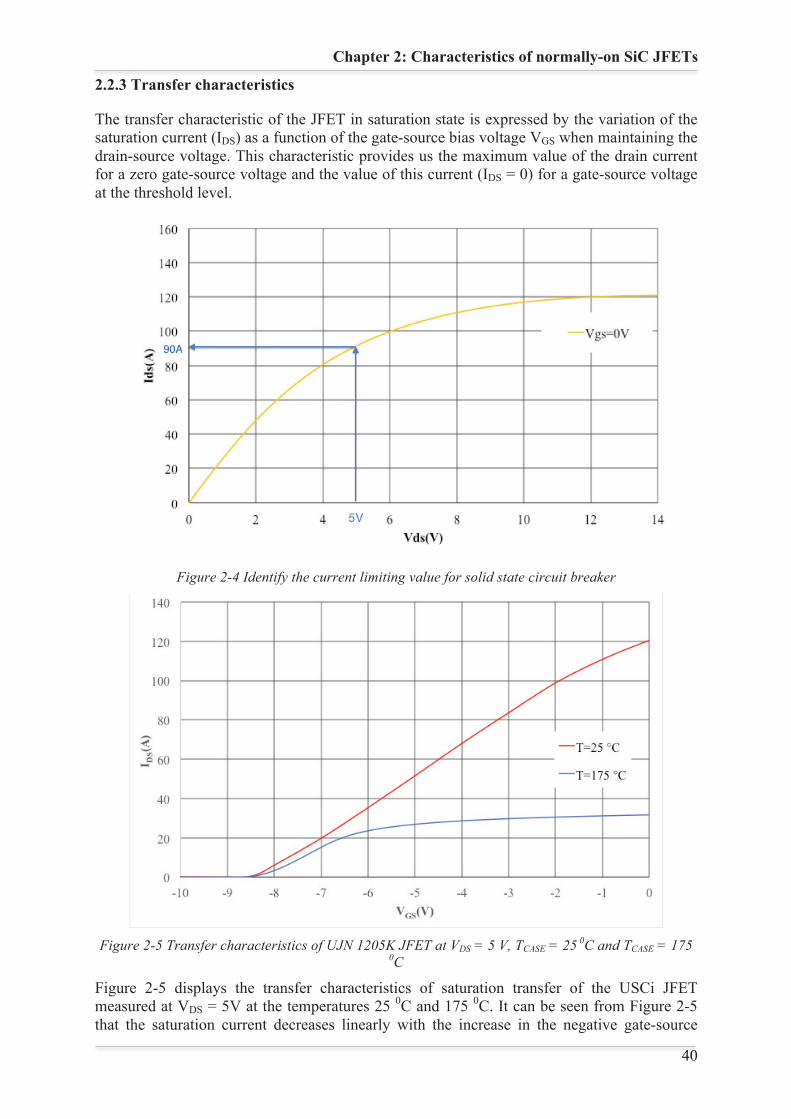
Chapter 2: Characteristics of normally-on SiC JFETs
40 40
2.2.3 Transfer characteristics
The transfer characteristic of the JFET in saturation state is expressed by the variation of the saturation current (IDS) as a function of the gate-source bias voltage VGS when maintaining the drain-source voltage. This characteristic provides us the maximum value of the drain current for a zero gate-source voltage and the value of this current (IDS = 0) for a gate-source voltage at the threshold level.
Figure 2-4 Identify the current limiting value for solid state circuit breaker
Figure 2-5 Transfer characteristics of UJN 1205K JFET at VDS = 5 V, TCASE = 25 0C and TCASE = 175
0C
Figure 2-5 displays the transfer characteristics of saturation transfer of the USCi JFET measured at VDS = 5V at the temperatures 25 0C and 175 0C. It can be seen from Figure 2-5 that the saturation current decreases linearly with the increase in the negative gate-source
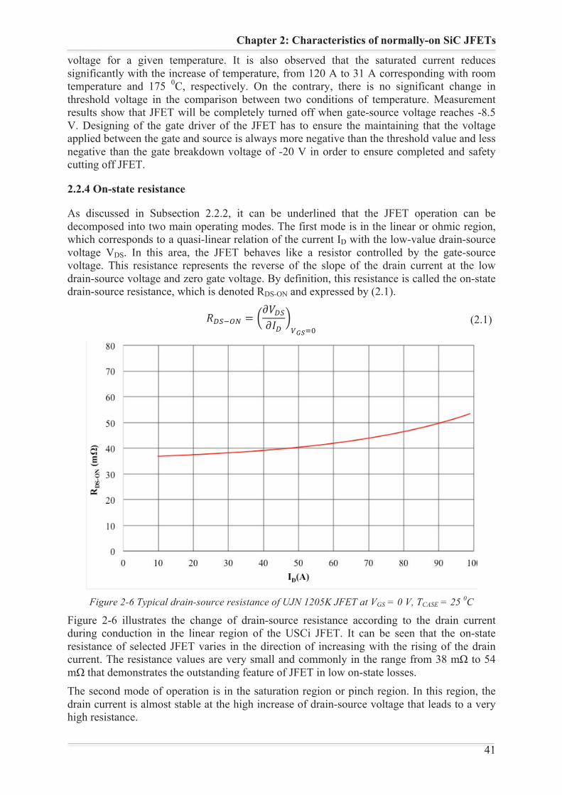
Chapter 2: Characteristics of normally-on SiC JFETs
41 41
voltage for a given temperature. It is also observed that the saturated current reduces significantly with the increase of temperature, from 120 A to 31 A corresponding with room temperature and 175 0C, respectively. On the contrary, there is no significant change in threshold voltage in the comparison between two conditions of temperature. Measurement results show that JFET will be completely turned off when gate-source voltage reaches -8.5 V. Designing of the gate driver of the JFET has to ensure the maintaining that the voltage applied between the gate and source is always more negative than the threshold value and less negative than the gate breakdown voltage of -20 V in order to ensure completed and safety cutting off JFET.
2.2.4 On-state resistance
As discussed in Subsection 2.2.2, it can be underlined that the JFET operation can be decomposed into two main operating modes. The first mode is in the linear or ohmic region, which corresponds to a quasi-linear relation of the current ID with the low-value drain-source voltage VDS. In this area, the JFET behaves like a resistor controlled by the gate-source voltage. This resistance represents the reverse of the slope of the drain current at the low drain-source voltage and zero gate voltage. By definition, this resistance is called the on-state drain-source resistance, which is denoted RDS-ON and expressed by (2.1).
(2.1)
Figure 2-6 Typical drain-source resistance of UJN 1205K JFET at VGS = 0 V, TCASE = 25 0C
Figure 2-6 illustrates the change of drain-source resistance according to the drain current during conduction in the linear region of the USCi JFET. It can be seen that the on-state resistance of selected JFET varies in the direction of increasing with the rising of the drain current. The resistance values are very small and commonly in the range from 38 mΩ to 54 mΩ that demonstrates the outstanding feature of JFET in low on-state losses. The second mode of operation is in the saturation region or pinch region. In this region, the drain current is almost stable at the high increase of drain-source voltage that leads to a very high resistance.
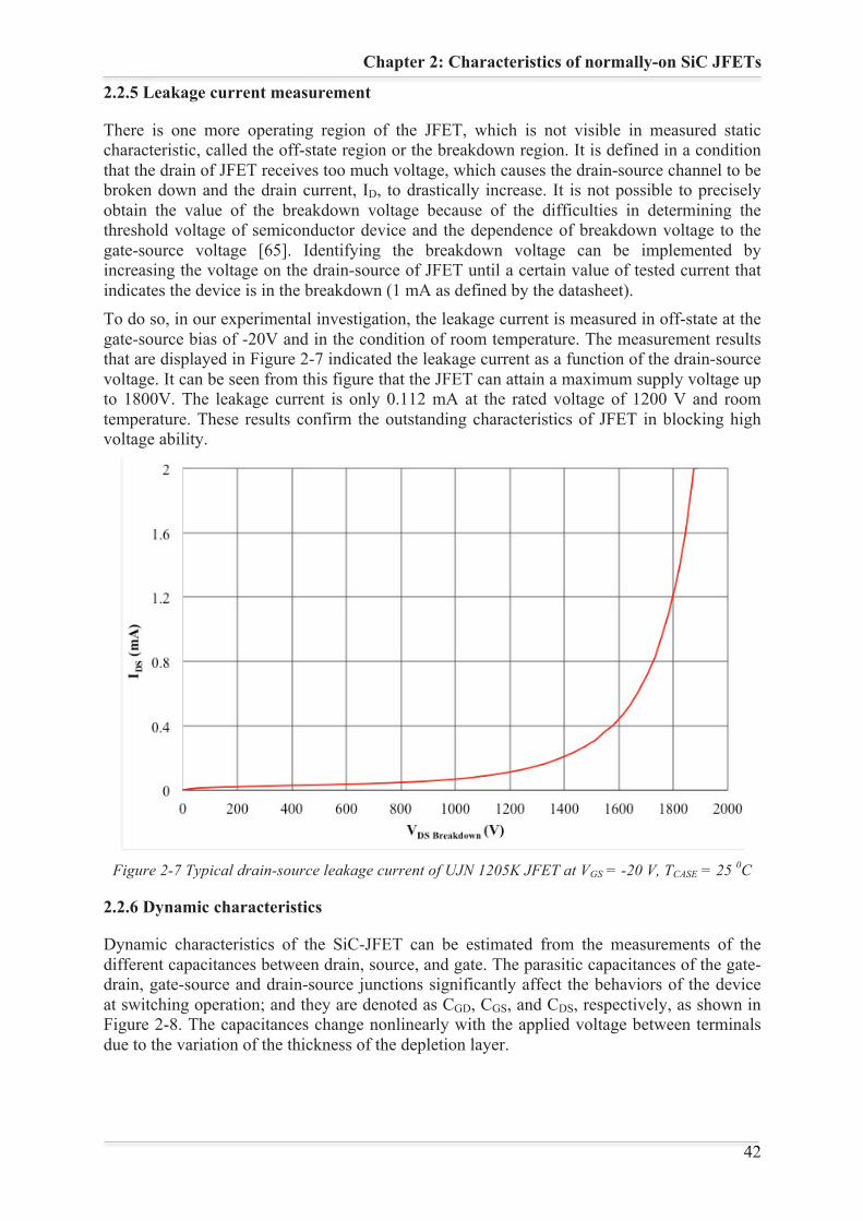
Chapter 2: Characteristics of normally-on SiC JFETs
42 42
2.2.5 Leakage current measurement
There is one more operating region of the JFET, which is not visible in measured static characteristic, called the off-state region or the breakdown region. It is defined in a condition that the drain of JFET receives too much voltage, which causes the drain-source channel to be broken down and the drain current, ID, to drastically increase. It is not possible to precisely obtain the value of the breakdown voltage because of the difficulties in determining the threshold voltage of semiconductor device and the dependence of breakdown voltage to the gate-source voltage [65]. Identifying the breakdown voltage can be implemented by increasing the voltage on the drain-source of JFET until a certain value of tested current that indicates the device is in the breakdown (1 mA as defined by the datasheet). To do so, in our experimental investigation, the leakage current is measured in off-state at the gate-source bias of -20V and in the condition of room temperature. The measurement results that are displayed in Figure 2-7 indicated the leakage current as a function of the drain-source voltage. It can be seen from this figure that the JFET can attain a maximum supply voltage up to 1800V. The leakage current is only 0.112 mA at the rated voltage of 1200 V and room temperature. These results confirm the outstanding characteristics of JFET in blocking high voltage ability.
Figure 2-7 Typical drain-source leakage current of UJN 1205K JFET at VGS = -20 V, TCASE = 25 0C
2.2.6 Dynamic characteristics
Dynamic characteristics of the SiC-JFET can be estimated from the measurements of the different capacitances between drain, source, and gate. The parasitic capacitances of the gate-drain, gate-source and drain-source junctions significantly affect the behaviors of the device at switching operation; and they are denoted as CGD, CGS, and CDS, respectively, as shown in Figure 2-8. The capacitances change nonlinearly with the applied voltage between terminals due to the variation of the thickness of the depletion layer.
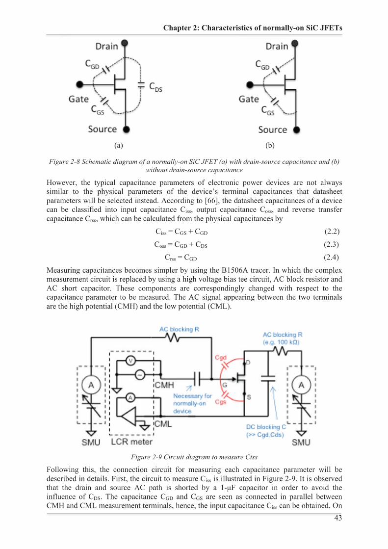
Chapter 2: Characteristics of normally-on SiC JFETs
43 43
(a)
(b)
Figure 2-8 Schematic diagram of a normally-on SiC JFET (a) with drain-source capacitance and (b) without drain-source capacitance
However, the typical capacitance parameters of electronic power devices are not always similar to the physical parameters of the device’s terminal capacitances that datasheet parameters will be selected instead. According to [66], the datasheet capacitances of a device can be classified into input capacitance Ciss, output capacitance Coss, and reverse transfer capacitance Crss, which can be calculated from the physical capacitances by Ciss = CGS + CGD (2.2)
Coss = CGD + CDS (2.3) Crss = CGD (2.4)
Measuring capacitances becomes simpler by using the B1506A tracer. In which the complex measurement circuit is replaced by using a high voltage bias tee circuit, AC block resistor and AC short capacitor. These components are correspondingly changed with respect to the capacitance parameter to be measured. The AC signal appearing between the two terminals are the high potential (CMH) and the low potential (CML).
Figure 2-9 Circuit diagram to measure Ciss
Following this, the connection circuit for measuring each capacitance parameter will be described in details. First, the circuit to measure Ciss is illustrated in Figure 2-9. It is observed that the drain and source AC path is shorted by a 1-μF capacitor in order to avoid the influence of CDS. The capacitance CGD and CGS are seen as connected in parallel between CMH and CML measurement terminals, hence, the input capacitance Ciss can be obtained. On
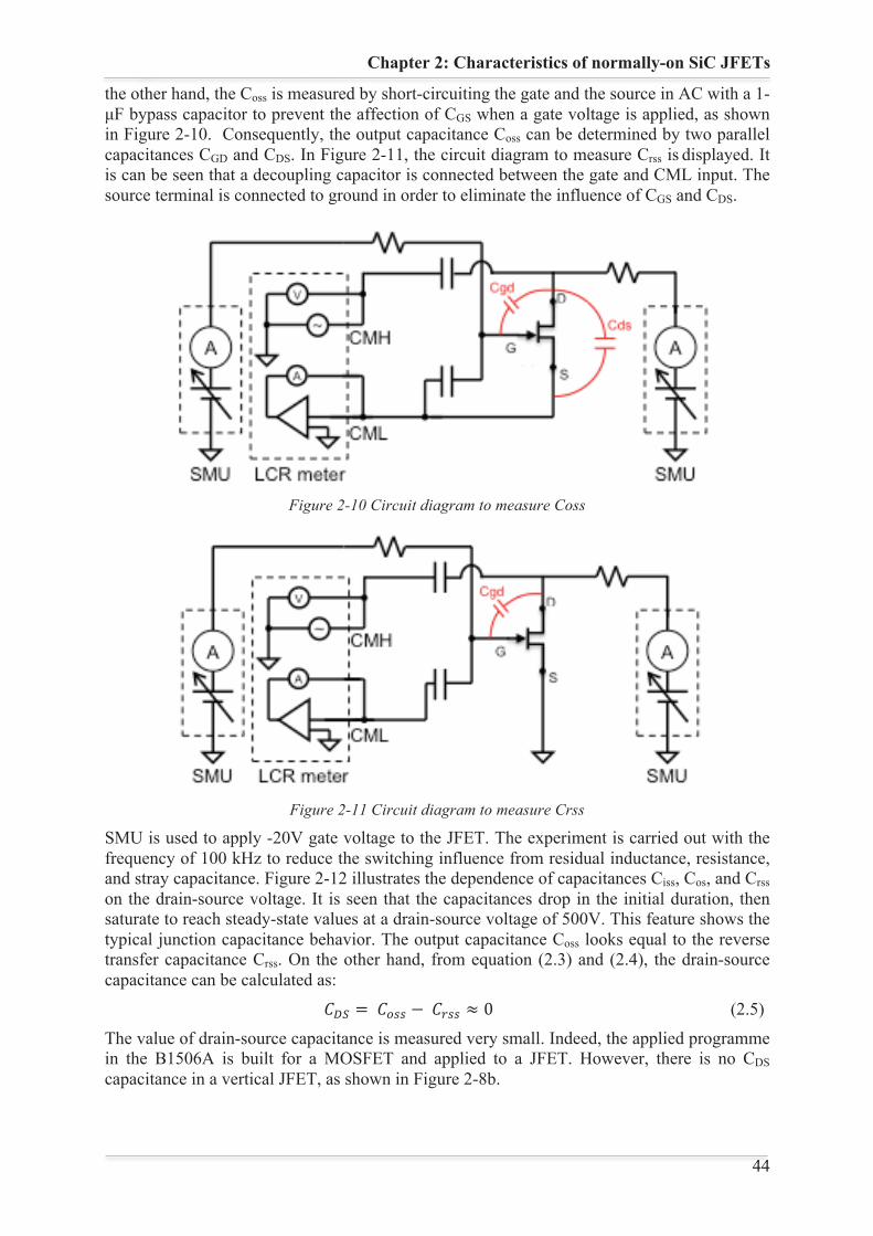
Chapter 2: Characteristics of normally-on SiC JFETs
44 44
the other hand, the Coss is measured by short-circuiting the gate and the source in AC with a 1-μF bypass capacitor to prevent the affection of CGS when a gate voltage is applied, as shown in Figure 2-10. Consequently, the output capacitance Coss can be determined by two parallel capacitances CGD and CDS. In Figure 2-11, the circuit diagram to measure Crss is displayed. It is can be seen that a decoupling capacitor is connected between the gate and CML input. The source terminal is connected to ground in order to eliminate the influence of CGS and CDS.
Figure 2-10 Circuit diagram to measure Coss
Figure 2-11 Circuit diagram to measure Crss
SMU is used to apply -20V gate voltage to the JFET. The experiment is carried out with the frequency of 100 kHz to reduce the switching influence from residual inductance, resistance, and stray capacitance. Figure 2-12 illustrates the dependence of capacitances Ciss, Cos, and Crss on the drain-source voltage. It is seen that the capacitances drop in the initial duration, then saturate to reach steady-state values at a drain-source voltage of 500V. This feature shows the typical junction capacitance behavior. The output capacitance Coss looks equal to the reverse transfer capacitance Crss. On the other hand, from equation (2.3) and (2.4), the drain-source capacitance can be calculated as:
(2.5)
The value of drain-source capacitance is measured very small. Indeed, the applied programme in the B1506A is built for a MOSFET and applied to a JFET. However, there is no CDS capacitance in a vertical JFET, as shown in Figure 2-8b.
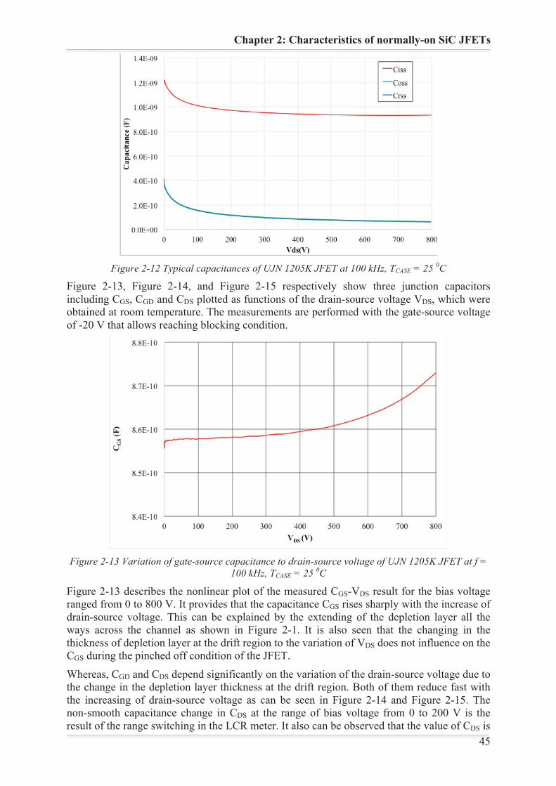
Chapter 2: Characteristics of normally-on SiC JFETs
45 45
Figure 2-12 Typical capacitances of UJN 1205K JFET at 100 kHz, TCASE = 25 0C
Figure 2-13, Figure 2-14, and Figure 2-15 respectively show three junction capacitors including CGS, CGD and CDS plotted as functions of the drain-source voltage VDS, which were obtained at room temperature. The measurements are performed with the gate-source voltage of -20 V that allows reaching blocking condition.
Figure 2-13 Variation of gate-source capacitance to drain-source voltage of UJN 1205K JFET at f =
100 kHz, TCASE = 25 0C
Figure 2-13 describes the nonlinear plot of the measured CGS-VDS result for the bias voltage ranged from 0 to 800 V. It provides that the capacitance CGS rises sharply with the increase of drain-source voltage. This can be explained by the extending of the depletion layer all the ways across the channel as shown in Figure 2-1. It is also seen that the changing in the thickness of depletion layer at the drift region to the variation of VDS does not influence on the CGS during the pinched off condition of the JFET.
Whereas, CGD and CDS depend significantly on the variation of the drain-source voltage due to the change in the depletion layer thickness at the drift region. Both of them reduce fast with the increasing of drain-source voltage as can be seen in Figure 2-14 and Figure 2-15. The non-smooth capacitance change in CDS at the range of bias voltage from 0 to 200 V is the result of the range switching in the LCR meter. It also can be observed that the value of CDS is
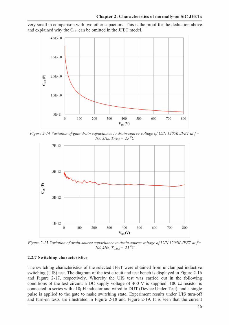
Chapter 2: Characteristics of normally-on SiC JFETs
46 46
very small in comparison with two other capacitors. This is the proof for the deduction above and explained why the CDS can be omitted in the JFET model.
Figure 2-14 Variation of gate-drain capacitance to drain-source voltage of UJN 1205K JFET at f =
100 kHz, TCASE = 25 0C
Figure 2-15 Variation of drain-source capacitance to drain-source voltage of UJN 1205K JFET at f =
100 kHz, TCASE = 25 0C
2.2.7 Switching characteristics
The switching characteristics of the selected JFET were obtained from unclamped inductive switching (UIS) test. The diagram of the test circuit and test bench is displayed in Figure 2-16 and Figure 2-17, respectively. Whereby the UIS test was carried out in the following conditions of the test circuit: a DC supply voltage of 400 V is supplied; 100 Ω resistor is connected in series with a10μH inductor and wired to DUT (Device Under Test), and a single pulse is applied to the gate to make switching state. Experiment results under UIS turn-off and turn-on tests are illustrated in Figure 2-18 and Figure 2-19. It is seen that the current
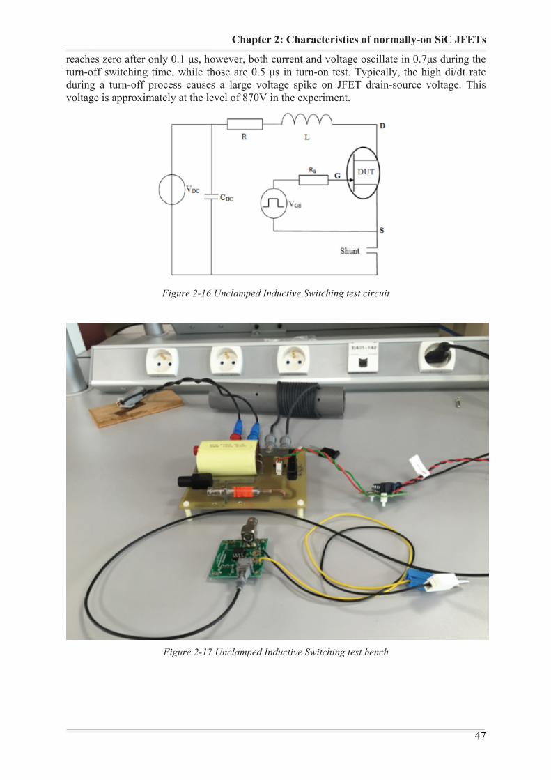
Chapter 2: Characteristics of normally-on SiC JFETs
47 47
reaches zero after only 0.1 μs, however, both current and voltage oscillate in 0.7μs during the turn-off switching time, while those are 0.5 μs in turn-on test. Typically, the high di/dt rate during a turn-off process causes a large voltage spike on JFET drain-source voltage. This voltage is approximately at the level of 870V in the experiment.
Figure 2-16 Unclamped Inductive Switching test circuit
Figure 2-17 Unclamped Inductive Switching test bench
Chapter 2: Characteristics of normally-on SiC JFETs
48 48
Figure 2-18 Turn off UJN 1205K JFET under single pulse unclamped inductive switching test
Figure 2-19 Turn on UJN 1205K JFET under single pulse unclamped inductive switching test
2.3 Robustness of normally-on SiC JFET
2.3.1 Short Circuit and Avalanche Breakdown Test Bench
A Short Circuit and Avalanche Breakdown Test Bench (SCAB) was set up in order to characterize the robustness of the SiC JFETs. The test bench consists of four main parts, in which Labview software is incorporated. The first one is the test circuit, which is configured in the diagram of short circuit test or avalanche test, respectively, as shown in Figure 2-20. The second part is a control desktop, where test modes and conditions are set up, such as short-circuit duration, number of pulses, etc., as seen in Figure 2-21. The test result can be observed on the oscilloscope in Figure 2-22. Optical fibers are used in order to connect and transmit data among above three parts as displayed in Figure 2-23.
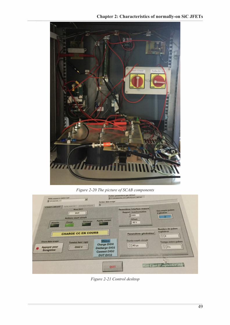
Chapter 2: Characteristics of normally-on SiC JFETs
49 49
Figure 2-20 The picture of SCAB components
Figure 2-21 Control desktop
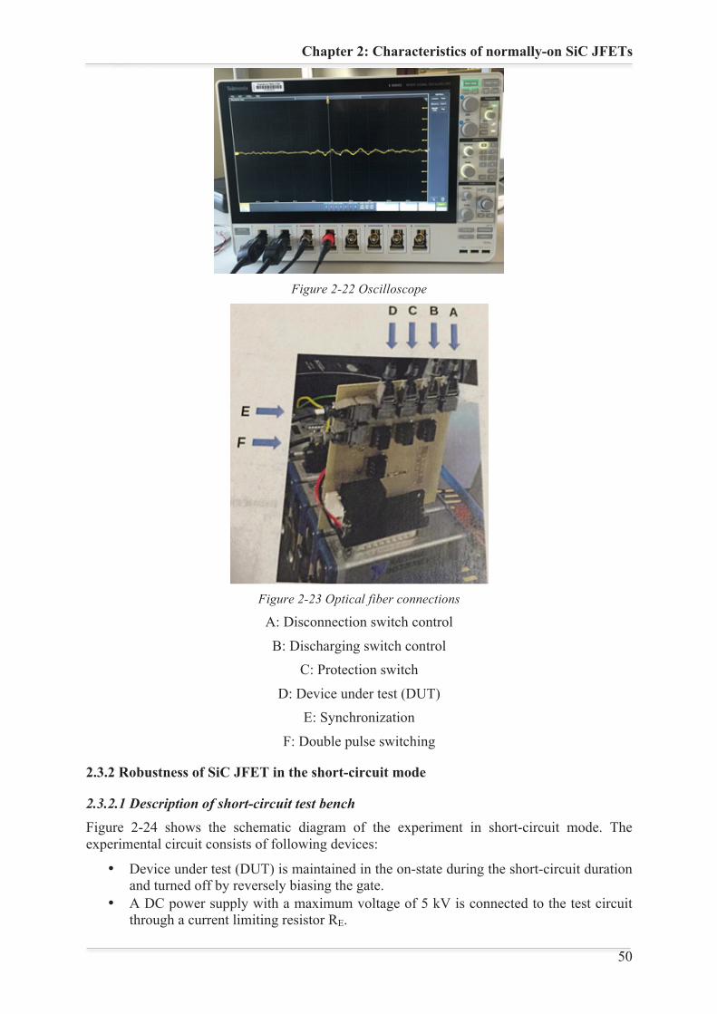
Chapter 2: Characteristics of normally-on SiC JFETs
50 50
Figure 2-22 Oscilloscope
Figure 2-23 Optical fiber connections
A: Disconnection switch control
B: Discharging switch control C: Protection switch
D: Device under test (DUT) E: Synchronization
F: Double pulse switching
2.3.2 Robustness of SiC JFET in the short-circuit mode
2.3.2.1 Description of short-circuit test bench Figure 2-24 shows the schematic diagram of the experiment in short-circuit mode. The experimental circuit consists of following devices:
• Device under test (DUT) is maintained in the on-state during the short-circuit duration and turned off by reversely biasing the gate.
• A DC power supply with a maximum voltage of 5 kV is connected to the test circuit through a current limiting resistor RE.
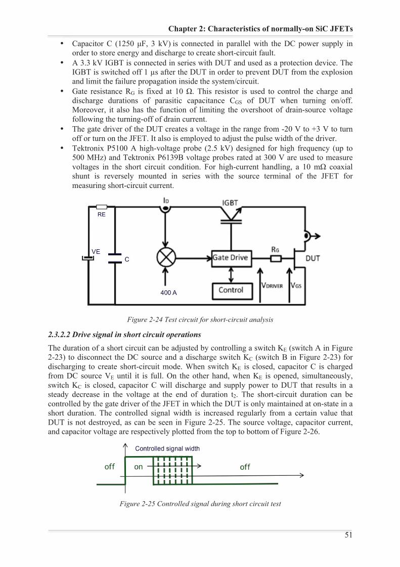
Chapter 2: Characteristics of normally-on SiC JFETs
51 51
• Capacitor C (1250 μF, 3 kV) is connected in parallel with the DC power supply in order to store energy and discharge to create short-circuit fault.
• A 3.3 kV IGBT is connected in series with DUT and used as a protection device. The IGBT is switched off 1 µs after the DUT in order to prevent DUT from the explosion and limit the failure propagation inside the system/circuit.
• Gate resistance RG is fixed at 10 Ω. This resistor is used to control the charge and discharge durations of parasitic capacitance CGS of DUT when turning on/off. Moreover, it also has the function of limiting the overshoot of drain-source voltage following the turning-off of drain current.
• The gate driver of the DUT creates a voltage in the range from -20 V to +3 V to turn off or turn on the JFET. It also is employed to adjust the pulse width of the driver.
• Tektronix P5100 A high-voltage probe (2.5 kV) designed for high frequency (up to 500 MHz) and Tektronix P6139B voltage probes rated at 300 V are used to measure voltages in the short circuit condition. For high-current handling, a 10 mΩ coaxial shunt is reversely mounted in series with the source terminal of the JFET for measuring short-circuit current.
Figure 2-24 Test circuit for short-circuit analysis
2.3.2.2 Drive signal in short circuit operations
The duration of a short circuit can be adjusted by controlling a switch KE (switch A in Figure 2-23) to disconnect the DC source and a discharge switch KC (switch B in Figure 2-23) for discharging to create short-circuit mode. When switch KE is closed, capacitor C is charged from DC source VE until it is full. On the other hand, when KE is opened, simultaneously, switch KC is closed, capacitor C will discharge and supply power to DUT that results in a steady decrease in the voltage at the end of duration t2. The short-circuit duration can be controlled by the gate driver of the JFET in which the DUT is only maintained at on-state in a short duration. The controlled signal width is increased regularly from a certain value that DUT is not destroyed, as can be seen in Figure 2-25. The source voltage, capacitor current, and capacitor voltage are respectively plotted from the top to bottom of Figure 2-26.
Figure 2-25 Controlled signal during short circuit test
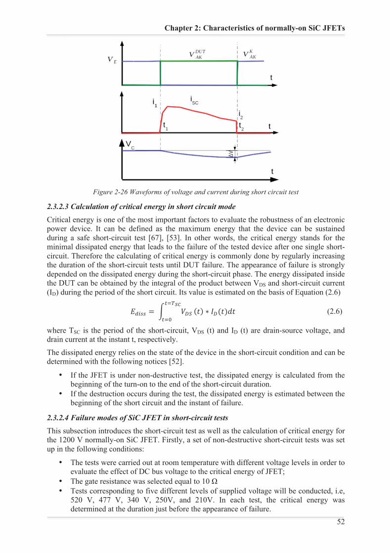
Chapter 2: Characteristics of normally-on SiC JFETs
52 52
Figure 2-26 Waveforms of voltage and current during short circuit test
2.3.2.3 Calculation of critical energy in short circuit mode
Critical energy is one of the most important factors to evaluate the robustness of an electronic power device. It can be defined as the maximum energy that the device can be sustained during a safe short-circuit test [67], [53]. In other words, the critical energy stands for the minimal dissipated energy that leads to the failure of the tested device after one single short-circuit. Therefore the calculating of critical energy is commonly done by regularly increasing the duration of the short-circuit tests until DUT failure. The appearance of failure is strongly depended on the dissipated energy during the short-circuit phase. The energy dissipated inside the DUT can be obtained by the integral of the product between VDS and short-circuit current (ID) during the period of the short circuit. Its value is estimated on the basis of Equation (2.6)
(2.6)
where TSC is the period of the short-circuit, VDS (t) and ID (t) are drain-source voltage, and drain current at the instant t, respectively.
The dissipated energy relies on the state of the device in the short-circuit condition and can be determined with the following notices [52].
• If the JFET is under non-destructive test, the dissipated energy is calculated from the beginning of the turn-on to the end of the short-circuit duration.
• If the destruction occurs during the test, the dissipated energy is estimated between the beginning of the short circuit and the instant of failure.
2.3.2.4 Failure modes of SiC JFET in short-circuit tests
This subsection introduces the short-circuit test as well as the calculation of critical energy for the 1200 V normally-on SiC JFET. Firstly, a set of non-destructive short-circuit tests was set up in the following conditions:
• The tests were carried out at room temperature with different voltage levels in order to evaluate the effect of DC bus voltage to the critical energy of JFET;
• The gate resistance was selected equal to 10 Ω • Tests corresponding to five different levels of supplied voltage will be conducted, i.e,
520 V, 477 V, 340 V, 250V, and 210V. In each test, the critical energy was determined at the duration just before the appearance of failure.
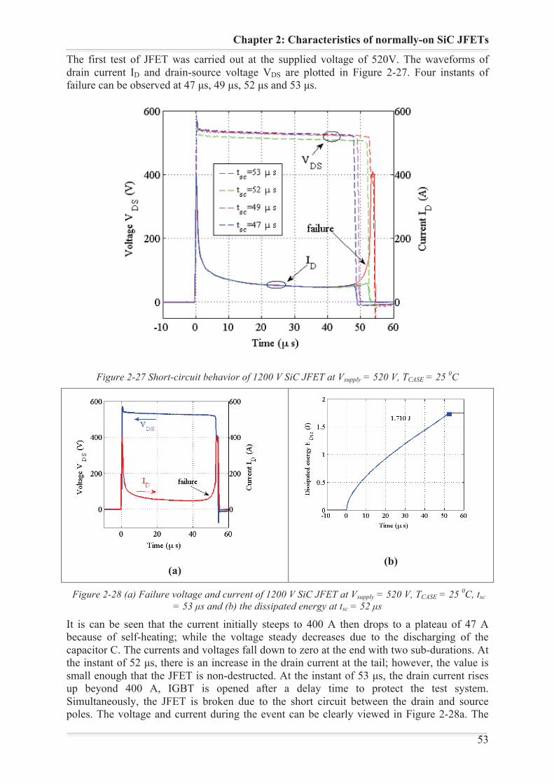
Chapter 2: Characteristics of normally-on SiC JFETs
53 53
The first test of JFET was carried out at the supplied voltage of 520V. The waveforms of drain current ID and drain-source voltage VDS are plotted in Figure 2-27. Four instants of failure can be observed at 47 μs, 49 μs, 52 μs and 53 μs.
Figure 2-27 Short-circuit behavior of 1200 V SiC JFET at Vsupply = 520 V, TCASE = 25 0C
(a)
(b)
Figure 2-28 (a) Failure voltage and current of 1200 V SiC JFET at Vsupply = 520 V, TCASE = 25 0C, tsc= 53 μs and (b) the dissipated energy at tsc = 52 μs
It is can be seen that the current initially steeps to 400 A then drops to a plateau of 47 A because of self-heating; while the voltage steady decreases due to the discharging of the capacitor C. The currents and voltages fall down to zero at the end with two sub-durations. At the instant of 52 μs, there is an increase in the drain current at the tail; however, the value is small enough that the JFET is non-destructed. At the instant of 53 μs, the drain current rises up beyond 400 A, IGBT is opened after a delay time to protect the test system. Simultaneously, the JFET is broken due to the short circuit between the drain and source poles. The voltage and current during the event can be clearly viewed in Figure 2-28a. The
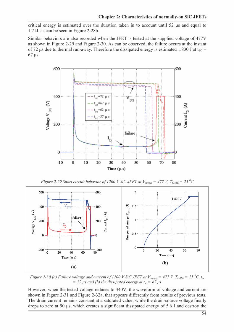
Chapter 2: Characteristics of normally-on SiC JFETs
54 54
critical energy is estimated over the duration taken in to account until 52 μs and equal to 1.71J, as can be seen in Figure 2-28b. Similar behaviors are also recorded when the JFET is tested at the supplied voltage of 477V as shown in Figure 2-29 and Figure 2-30. As can be observed, the failure occurs at the instant of 72 μs due to thermal run-away. Therefore the dissipated energy is estimated 1.830 J at tSC = 67 μs.
Figure 2-29 Short circuit behavior of 1200 V SiC JFET at Vsupply = 477 V, TCASE = 25 0C
(a)
(b)
Figure 2-30 (a) Failure voltage and current of 1200 V SiC JFET at Vsupply = 477 V, TCASE = 25 0C, tsc = 72 μs and (b) the dissipated energy at tsc = 67 μs
However, when the tested voltage reduces to 340V, the waveform of voltage and current are shown in Figure 2-31 and Figure 2-32a, that appears differently from results of previous tests. The drain current remains constant at a saturated value; while the drain-source voltage finally drops to zero at 90 μs, which creates a significant dissipated energy of 5.6 J and destroy the
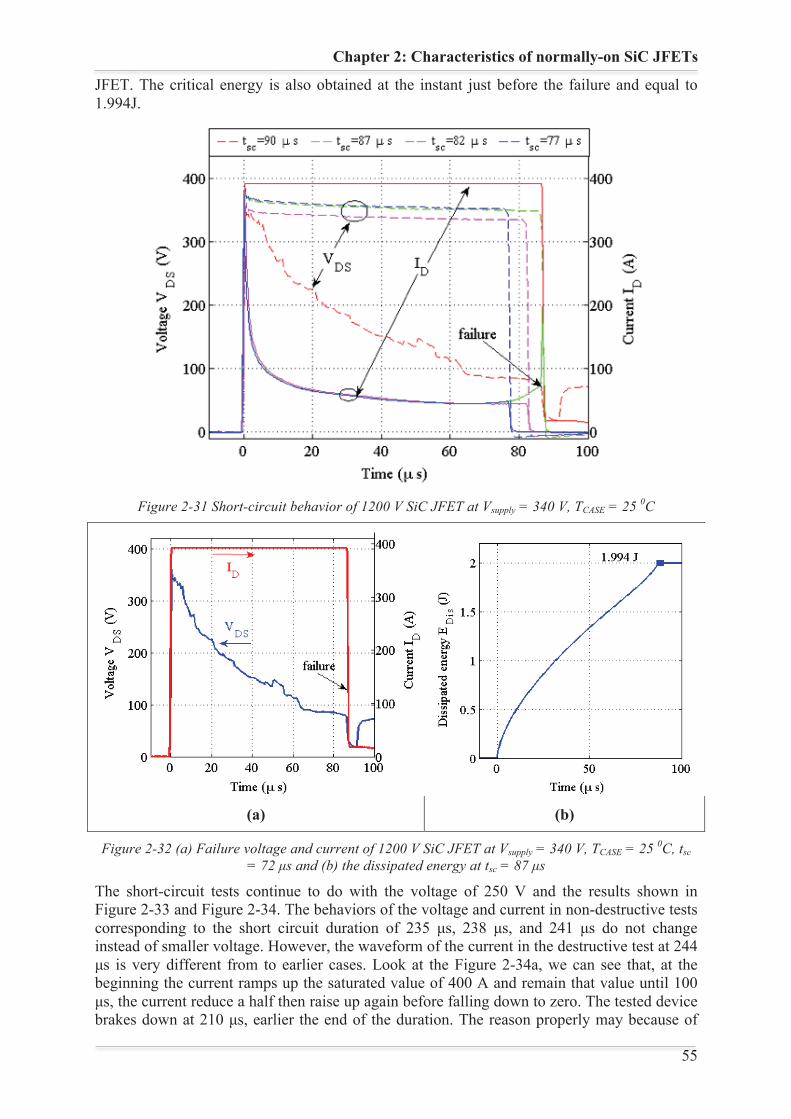
Chapter 2: Characteristics of normally-on SiC JFETs
55 55
JFET. The critical energy is also obtained at the instant just before the failure and equal to 1.994J.
Figure 2-31 Short-circuit behavior of 1200 V SiC JFET at Vsupply = 340 V, TCASE = 25 0C
(a) (b)
Figure 2-32 (a) Failure voltage and current of 1200 V SiC JFET at Vsupply = 340 V, TCASE = 25 0C, tsc = 72 μs and (b) the dissipated energy at tsc = 87 μs
The short-circuit tests continue to do with the voltage of 250 V and the results shown in Figure 2-33 and Figure 2-34. The behaviors of the voltage and current in non-destructive tests corresponding to the short circuit duration of 235 μs, 238 μs, and 241 μs do not change instead of smaller voltage. However, the waveform of the current in the destructive test at 244 μs is very different from to earlier cases. Look at the Figure 2-34a, we can see that, at the beginning the current ramps up the saturated value of 400 A and remain that value until 100 μs, the current reduce a half then raise up again before falling down to zero. The tested device brakes down at 210 μs, earlier the end of the duration. The reason properly may because of
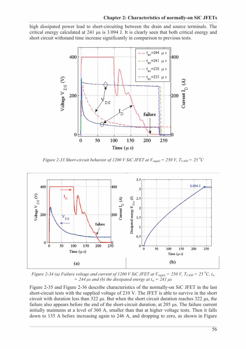
Chapter 2: Characteristics of normally-on SiC JFETs
56 56
high dissipated power lead to short-circuiting between the drain and source terminals. The critical energy calculated at 241 μs is 3.094 J. It is clearly seen that both critical energy and short circuit withstand time increase significantly in comparison to previous tests.
Figure 2-33 Short-circuit behavior of 1200 V SiC JFET at Vsupply = 250 V, TCASE = 25 0C
(a) (b)
Figure 2-34 (a) Failure voltage and current of 1200 V SiC JFET at Vsupply = 250 V, TCASE = 25 0C, tsc = 244 μs and (b) the dissipated energy at tsc = 241 μs
Figure 2-35 and Figure 2-36 describe characteristics of the normally-on SiC JFET in the last short-circuit tests with the supplied voltage of 210 V. The JFET is able to survive in the short circuit with duration less than 322 μs. But when the short circuit duration reaches 322 μs, the failure also appears before the end of the short-circuit duration, at 205 μs. The failure current initially maintains at a level of 360 A, smaller than that at higher voltage tests. Then it falls down to 135 A before increasing again to 246 A, and dropping to zero, as shown in Figure
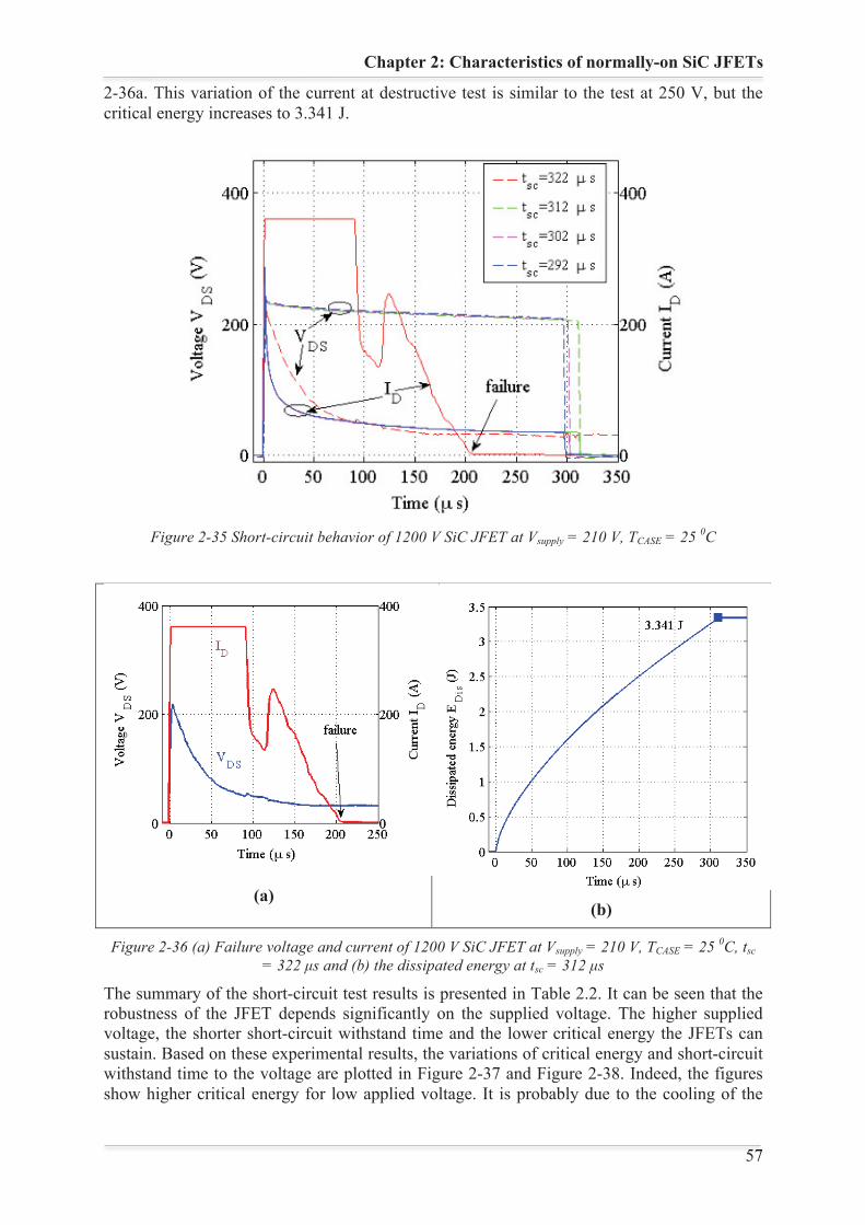
Chapter 2: Characteristics of normally-on SiC JFETs
57 57
2-36a. This variation of the current at destructive test is similar to the test at 250 V, but the critical energy increases to 3.341 J.
Figure 2-35 Short-circuit behavior of 1200 V SiC JFET at Vsupply = 210 V, TCASE = 25 0C
(a) (b)
Figure 2-36 (a) Failure voltage and current of 1200 V SiC JFET at Vsupply = 210 V, TCASE = 25 0C, tsc = 322 μs and (b) the dissipated energy at tsc = 312 μs
The summary of the short-circuit test results is presented in Table 2.2. It can be seen that the robustness of the JFET depends significantly on the supplied voltage. The higher supplied voltage, the shorter short-circuit withstand time and the lower critical energy the JFETs can sustain. Based on these experimental results, the variations of critical energy and short-circuit withstand time to the voltage are plotted in Figure 2-37 and Figure 2-38. Indeed, the figures show higher critical energy for low applied voltage. It is probably due to the cooling of the
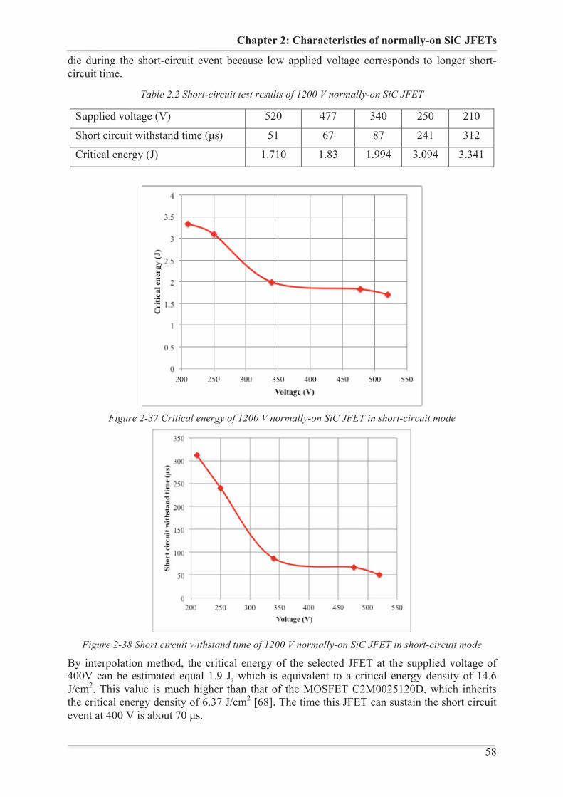
Chapter 2: Characteristics of normally-on SiC JFETs
58 58
die during the short-circuit event because low applied voltage corresponds to longer short-circuit time.
Table 2.2 Short-circuit test results of 1200 V normally-on SiC JFET
Supplied voltage (V) 520 477 340 250 210
Short circuit withstand time (μs) 51 67 87 241 312
Critical energy (J) 1.710 1.83 1.994 3.094 3.341
Figure 2-37 Critical energy of 1200 V normally-on SiC JFET in short-circuit mode
Figure 2-38 Short circuit withstand time of 1200 V normally-on SiC JFET in short-circuit mode
By interpolation method, the critical energy of the selected JFET at the supplied voltage of 400V can be estimated equal 1.9 J, which is equivalent to a critical energy density of 14.6 J/cm2. This value is much higher than that of the MOSFET C2M0025120D, which inherits the critical energy density of 6.37 J/cm2 [68]. The time this JFET can sustain the short circuit event at 400 V is about 70 μs.
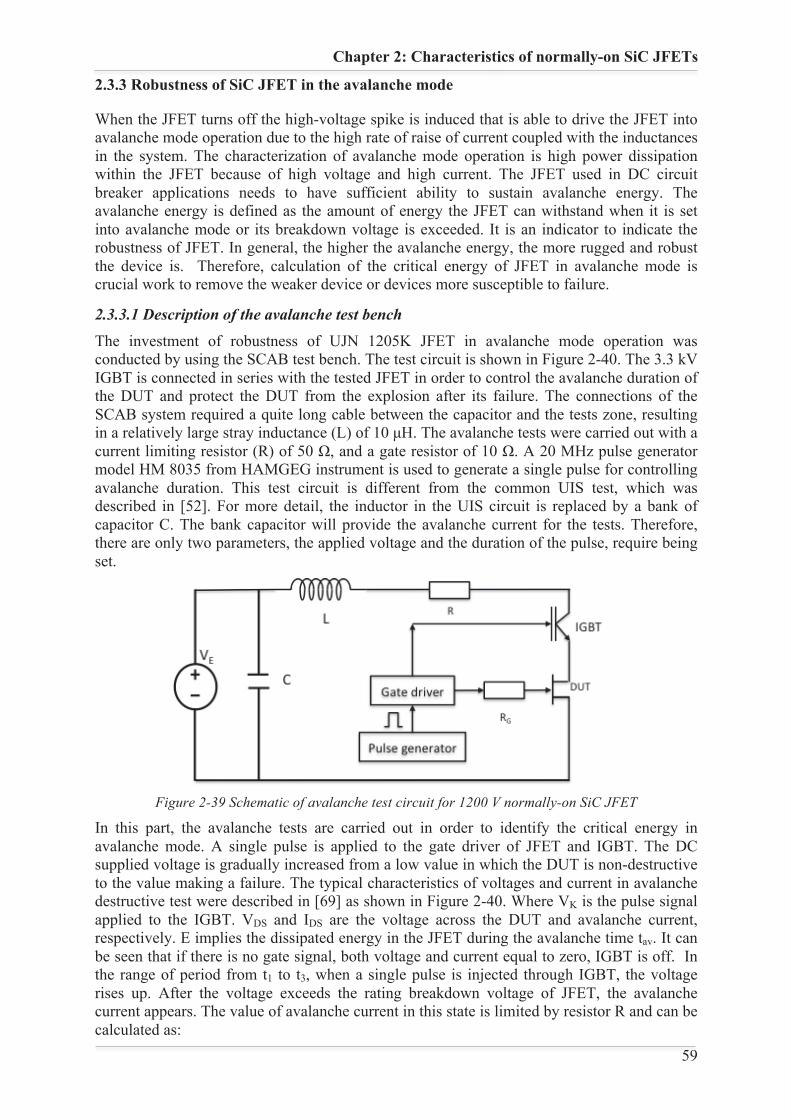
Chapter 2: Characteristics of normally-on SiC JFETs
59 59
2.3.3 Robustness of SiC JFET in the avalanche mode
When the JFET turns off the high-voltage spike is induced that is able to drive the JFET into avalanche mode operation due to the high rate of raise of current coupled with the inductances in the system. The characterization of avalanche mode operation is high power dissipation within the JFET because of high voltage and high current. The JFET used in DC circuit breaker applications needs to have sufficient ability to sustain avalanche energy. The avalanche energy is defined as the amount of energy the JFET can withstand when it is set into avalanche mode or its breakdown voltage is exceeded. It is an indicator to indicate the robustness of JFET. In general, the higher the avalanche energy, the more rugged and robust the device is. Therefore, calculation of the critical energy of JFET in avalanche mode is crucial work to remove the weaker device or devices more susceptible to failure.
2.3.3.1 Description of the avalanche test bench
The investment of robustness of UJN 1205K JFET in avalanche mode operation was conducted by using the SCAB test bench. The test circuit is shown in Figure 2-40. The 3.3 kV IGBT is connected in series with the tested JFET in order to control the avalanche duration of the DUT and protect the DUT from the explosion after its failure. The connections of the SCAB system required a quite long cable between the capacitor and the tests zone, resulting in a relatively large stray inductance (L) of 10 μH. The avalanche tests were carried out with a current limiting resistor (R) of 50 Ω, and a gate resistor of 10 Ω. A 20 MHz pulse generator model HM 8035 from HAMGEG instrument is used to generate a single pulse for controlling avalanche duration. This test circuit is different from the common UIS test, which was described in [52]. For more detail, the inductor in the UIS circuit is replaced by a bank of capacitor C. The bank capacitor will provide the avalanche current for the tests. Therefore, there are only two parameters, the applied voltage and the duration of the pulse, require being set.
Figure 2-39 Schematic of avalanche test circuit for 1200 V normally-on SiC JFET
In this part, the avalanche tests are carried out in order to identify the critical energy in avalanche mode. A single pulse is applied to the gate driver of JFET and IGBT. The DC supplied voltage is gradually increased from a low value in which the DUT is non-destructive to the value making a failure. The typical characteristics of voltages and current in avalanche destructive test were described in [69] as shown in Figure 2-40. Where VK is the pulse signal applied to the IGBT. VDS and IDS are the voltage across the DUT and avalanche current, respectively. E implies the dissipated energy in the JFET during the avalanche time tav. It can be seen that if there is no gate signal, both voltage and current equal to zero, IGBT is off. In the range of period from t1 to t3, when a single pulse is injected through IGBT, the voltage rises up. After the voltage exceeds the rating breakdown voltage of JFET, the avalanche current appears. The value of avalanche current in this state is limited by resistor R and can be calculated as:
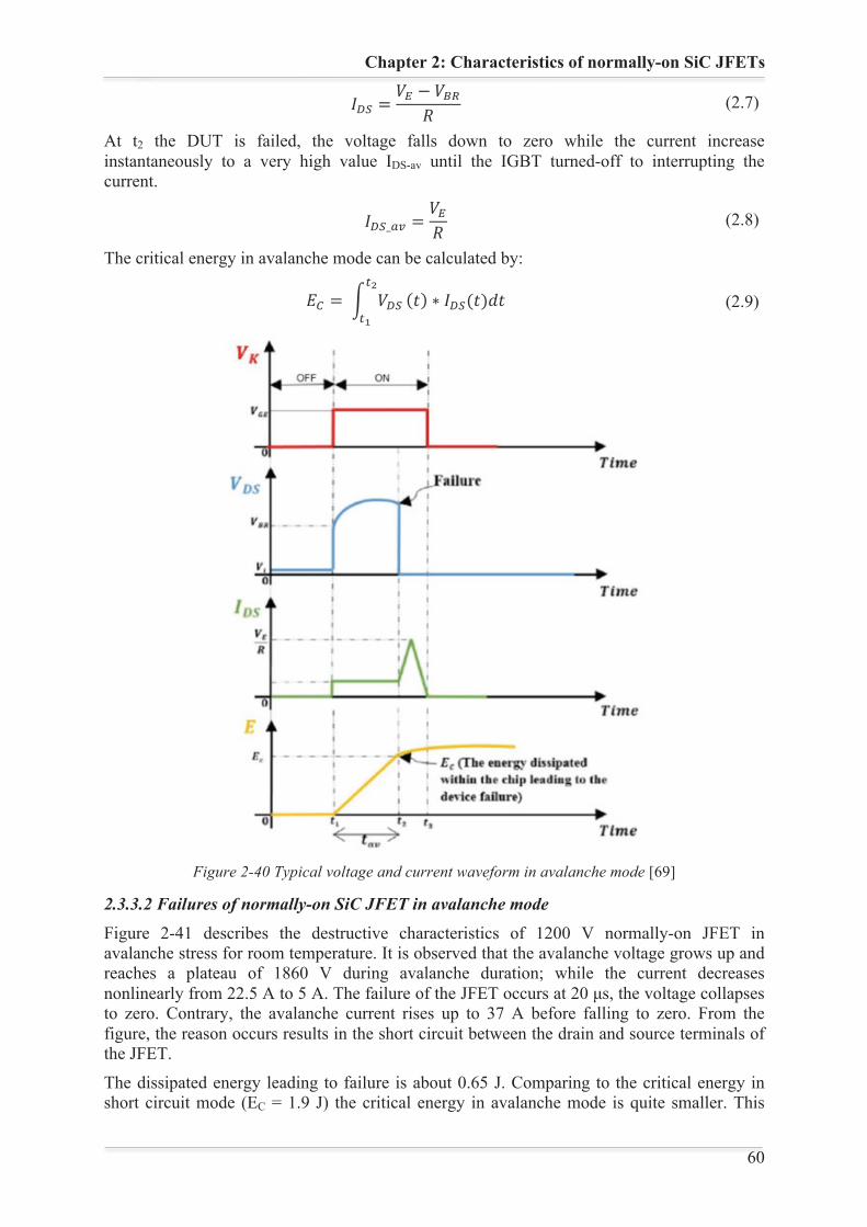
Chapter 2: Characteristics of normally-on SiC JFETs
60 60
(2.7)
At t2 the DUT is failed, the voltage falls down to zero while the current increase instantaneously to a very high value IDS-av until the IGBT turned-off to interrupting the current.
(2.8)
The critical energy in avalanche mode can be calculated by:
(2.9)
Figure 2-40 Typical voltage and current waveform in avalanche mode [69]
2.3.3.2 Failures of normally-on SiC JFET in avalanche mode
Figure 2-41 describes the destructive characteristics of 1200 V normally-on JFET in avalanche stress for room temperature. It is observed that the avalanche voltage grows up and reaches a plateau of 1860 V during avalanche duration; while the current decreases nonlinearly from 22.5 A to 5 A. The failure of the JFET occurs at 20 μs, the voltage collapses to zero. Contrary, the avalanche current rises up to 37 A before falling to zero. From the figure, the reason occurs results in the short circuit between the drain and source terminals of the JFET.
The dissipated energy leading to failure is about 0.65 J. Comparing to the critical energy in short circuit mode (EC = 1.9 J) the critical energy in avalanche mode is quite smaller. This
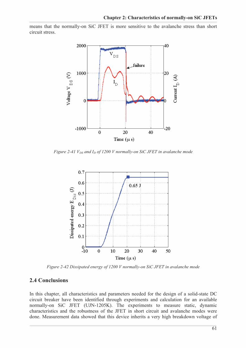
Chapter 2: Characteristics of normally-on SiC JFETs
61 61
means that the normally-on SiC JFET is more sensitive to the avalanche stress than short circuit stress.
Figure 2-41 VDS and ID of 1200 V normally-on SiC JFET in avalanche mode
Figure 2-42 Dissipated energy of 1200 V normally-on SiC JFET in avalanche mode
2.4 Conclusions
In this chapter, all characteristics and parameters needed for the design of a solid-state DC circuit breaker have been identified through experiments and calculation for an available normally-on SiC JFET (UJN-1205K). The experiments to measure static, dynamic characteristics and the robustness of the JFET in short circuit and avalanche modes were done. Measurement data showed that this device inherits a very high breakdown voltage of

Chapter 2: Characteristics of normally-on SiC JFETs
62 62
1800 V (at the gate voltage of -20 V), and small on-resistance of 45 mΩ and a gate threshold voltage of -8.5V, those prove the great suitable for SSCB applications. Although the critical energy in avalanche mode was determined by the tests with the value 0.65 J in the duration of 20 μs is much smaller than that in short-circuit operating mode (1.9 J at short circuit duration of 70 μs), it still confirms the robustness of the JFET. In next chapter, the design and operating principle of a solid state DC circuit breaker will be proposed.
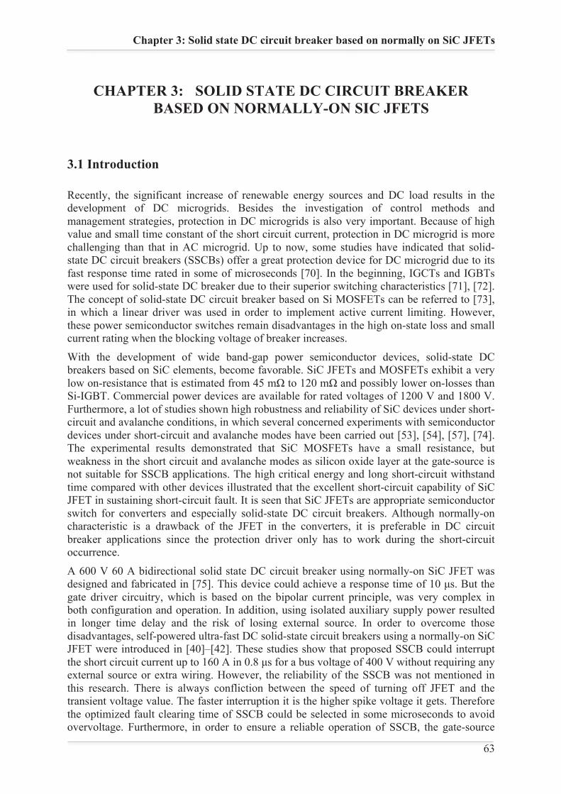
Chapter 3: Solid state DC circuit breaker based on normally on SiC JFETs
63 63
CHAPTER 3: SOLID STATE DC CIRCUIT BREAKER BASED ON NORMALLY-ON SIC JFETS
3.1 Introduction
Recently, the significant increase of renewable energy sources and DC load results in the development of DC microgrids. Besides the investigation of control methods and management strategies, protection in DC microgrids is also very important. Because of high value and small time constant of the short circuit current, protection in DC microgrid is more challenging than that in AC microgrid. Up to now, some studies have indicated that solid-state DC circuit breakers (SSCBs) offer a great protection device for DC microgrid due to its fast response time rated in some of microseconds [70]. In the beginning, IGCTs and IGBTs were used for solid-state DC breaker due to their superior switching characteristics [71], [72]. The concept of solid-state DC circuit breaker based on Si MOSFETs can be referred to [73], in which a linear driver was used in order to implement active current limiting. However, these power semiconductor switches remain disadvantages in the high on-state loss and small current rating when the blocking voltage of breaker increases.
With the development of wide band-gap power semiconductor devices, solid-state DC breakers based on SiC elements, become favorable. SiC JFETs and MOSFETs exhibit a very low on-resistance that is estimated from 45 mΩ to 120 mΩ and possibly lower on-losses than Si-IGBT. Commercial power devices are available for rated voltages of 1200 V and 1800 V. Furthermore, a lot of studies shown high robustness and reliability of SiC devices under short-circuit and avalanche conditions, in which several concerned experiments with semiconductor devices under short-circuit and avalanche modes have been carried out [53], [54], [57], [74]. The experimental results demonstrated that SiC MOSFETs have a small resistance, but weakness in the short circuit and avalanche modes as silicon oxide layer at the gate-source is not suitable for SSCB applications. The high critical energy and long short-circuit withstand time compared with other devices illustrated that the excellent short-circuit capability of SiC JFET in sustaining short-circuit fault. It is seen that SiC JFETs are appropriate semiconductor switch for converters and especially solid-state DC circuit breakers. Although normally-on characteristic is a drawback of the JFET in the converters, it is preferable in DC circuit breaker applications since the protection driver only has to work during the short-circuit occurrence.
A 600 V 60 A bidirectional solid state DC circuit breaker using normally-on SiC JFET was designed and fabricated in [75]. This device could achieve a response time of 10 μs. But the gate driver circuitry, which is based on the bipolar current principle, was very complex in both configuration and operation. In addition, using isolated auxiliary supply power resulted in longer time delay and the risk of losing external source. In order to overcome those disadvantages, self-powered ultra-fast DC solid-state circuit breakers using a normally-on SiC JFET were introduced in [40]–[42]. These studies show that proposed SSCB could interrupt the short circuit current up to 160 A in 0.8 μs for a bus voltage of 400 V without requiring any external source or extra wiring. However, the reliability of the SSCB was not mentioned in this research. There is always confliction between the speed of turning off JFET and the transient voltage value. The faster interruption it is the higher spike voltage it gets. Therefore the optimized fault clearing time of SSCB could be selected in some microseconds to avoid overvoltage. Furthermore, in order to ensure a reliable operation of SSCB, the gate-source
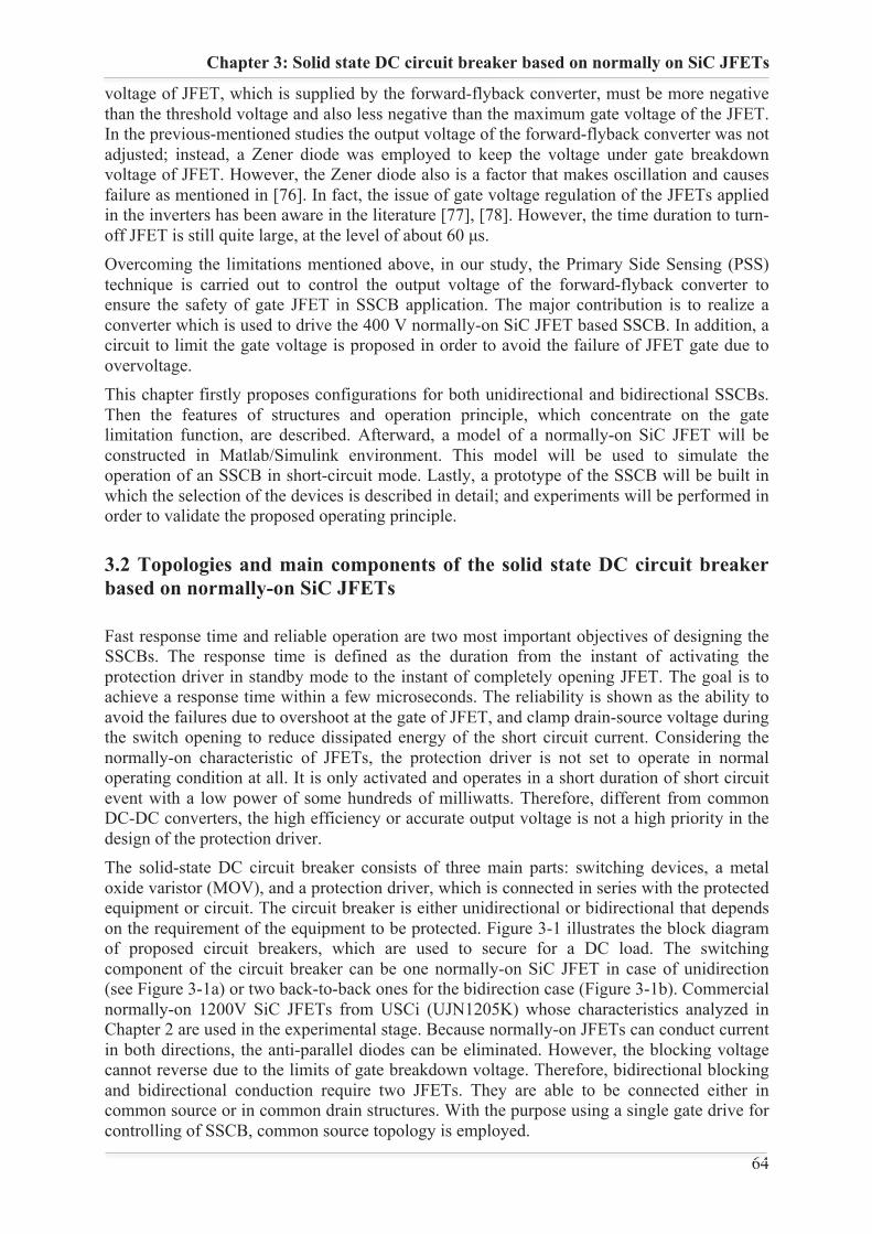
Chapter 3: Solid state DC circuit breaker based on normally on SiC JFETs
64 64
voltage of JFET, which is supplied by the forward-flyback converter, must be more negative than the threshold voltage and also less negative than the maximum gate voltage of the JFET. In the previous-mentioned studies the output voltage of the forward-flyback converter was not adjusted; instead, a Zener diode was employed to keep the voltage under gate breakdown voltage of JFET. However, the Zener diode also is a factor that makes oscillation and causes failure as mentioned in [76]. In fact, the issue of gate voltage regulation of the JFETs applied in the inverters has been aware in the literature [77], [78]. However, the time duration to turn-off JFET is still quite large, at the level of about 60 μs. Overcoming the limitations mentioned above, in our study, the Primary Side Sensing (PSS) technique is carried out to control the output voltage of the forward-flyback converter to ensure the safety of gate JFET in SSCB application. The major contribution is to realize a converter which is used to drive the 400 V normally-on SiC JFET based SSCB. In addition, a circuit to limit the gate voltage is proposed in order to avoid the failure of JFET gate due to overvoltage. This chapter firstly proposes configurations for both unidirectional and bidirectional SSCBs. Then the features of structures and operation principle, which concentrate on the gate limitation function, are described. Afterward, a model of a normally-on SiC JFET will be constructed in Matlab/Simulink environment. This model will be used to simulate the operation of an SSCB in short-circuit mode. Lastly, a prototype of the SSCB will be built in which the selection of the devices is described in detail; and experiments will be performed in order to validate the proposed operating principle.
3.2 Topologies and main components of the solid state DC circuit breaker based on normally-on SiC JFETs
Fast response time and reliable operation are two most important objectives of designing the SSCBs. The response time is defined as the duration from the instant of activating the protection driver in standby mode to the instant of completely opening JFET. The goal is to achieve a response time within a few microseconds. The reliability is shown as the ability to avoid the failures due to overshoot at the gate of JFET, and clamp drain-source voltage during the switch opening to reduce dissipated energy of the short circuit current. Considering the normally-on characteristic of JFETs, the protection driver is not set to operate in normal operating condition at all. It is only activated and operates in a short duration of short circuit event with a low power of some hundreds of milliwatts. Therefore, different from common DC-DC converters, the high efficiency or accurate output voltage is not a high priority in the design of the protection driver. The solid-state DC circuit breaker consists of three main parts: switching devices, a metal oxide varistor (MOV), and a protection driver, which is connected in series with the protected equipment or circuit. The circuit breaker is either unidirectional or bidirectional that depends on the requirement of the equipment to be protected. Figure 3-1 illustrates the block diagram of proposed circuit breakers, which are used to secure for a DC load. The switching component of the circuit breaker can be one normally-on SiC JFET in case of unidirection (see Figure 3-1a) or two back-to-back ones for the bidirection case (Figure 3-1b). Commercial normally-on 1200V SiC JFETs from USCi (UJN1205K) whose characteristics analyzed in Chapter 2 are used in the experimental stage. Because normally-on JFETs can conduct current in both directions, the anti-parallel diodes can be eliminated. However, the blocking voltage cannot reverse due to the limits of gate breakdown voltage. Therefore, bidirectional blocking and bidirectional conduction require two JFETs. They are able to be connected either in common source or in common drain structures. With the purpose using a single gate drive for controlling of SSCB, common source topology is employed.
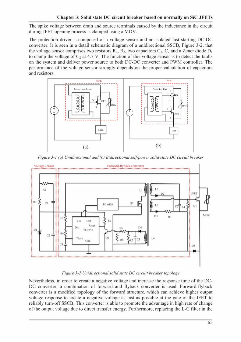
Chapter 3: Solid state DC circuit breaker based on normally on SiC JFETs
65 65
The spike voltage between drain and source terminals caused by the inductance in the circuit during JFET opening process is clamped using a MOV. The protection driver is composed of a voltage sensor and an isolated fast starting DC-DC converter. It is seen in a detail schematic diagram of a unidirectional SSCB, Figure 3-2, that the voltage sensor comprises two resistors R1, R2, two capacitors C1, C2 and a Zener diode D1 to clamp the voltage of C2 at 4.7 V. The function of this voltage sensor is to detect the faults on the system and deliver power source to both DC-DC converter and PWM controller. The performance of the voltage sensor strongly depends on the proper calculation of capacitors and resistors.
(a)
(b)
Figure 3-1 (a) Unidirectional and (b) Bidirectional self-power solid state DC circuit breaker
Figure 3-2 Unidirectional solid state DC circuit breaker topology
Nevertheless, in order to create a negative voltage and increase the response time of the DC-DC converter, a combination of forward and flyback converter is used. Forward-flyback converter is a modified topology of the forward structure, which can achieve higher output voltage response to create a negative voltage as fast as possible at the gate of the JFET to reliably turn-off SSCB. This converter is able to promote the advantage in high rate of change of the output voltage due to direct transfer energy. Furthermore, replacing the L-C filter in the
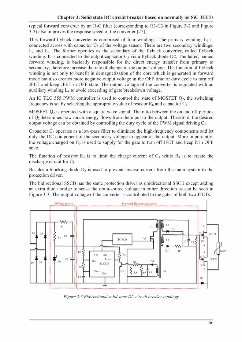
Chapter 3: Solid state DC circuit breaker based on normally on SiC JFETs
66 66
typical forward converter by an R-C filter (corresponding to R3-C3 in Figure 3-2 and Figure 3-3) also improves the response speed of the converter [77]. This forward-flyback converter is comprised of four windings. The primary winding L1 is connected across with capacitor C2 of the voltage sensor. There are two secondary windings: L2 and L3. The former operates as the secondary of the flyback converter, called flyback winding. It is connected to the output capacitor C3 via a flyback diode D2. The latter, named forward winding, is basically responsible for the direct energy transfer from primary to secondary, therefore increase the rate of change of the output voltage. The function of flyback winding is not only to benefit in demagnetization of the core which is generated in forward mode but also creates more negative output voltage in the OFF time of duty cycle to turn off JFET and keep JFET in OFF state. The output voltage of the converter is regulated with an auxiliary winding L4 to avoid exceeding of gate breakdown voltage. An IC TLC 555 PWM controller is used to control the state of MOSFET Q2, the switching frequency is set by selecting the appropriate value of resistor R6 and capacitor C4. MOSFET Q2 is operated with a square wave signal. The ratio between the on and off periods of Q2 determines how much energy flows from the input to the output. Therefore, the desired output voltage can be obtained by controlling the duty cycle of the PWM signal driving Q2.
Capacitor C3 operates as a low-pass filter to eliminate the high-frequency components and let only the DC component of the secondary voltage to appear at the output. More importantly, the voltage charged on C3 is used to supply for the gate to turn off JFET and keep it in OFF state.
The function of resistor R3 is to limit the charge current of C3 while R4 is to create the discharge circuit for C3.
Besides a blocking diode D5 is used to prevent inverse current from the main system to the protection driver.
The bidirectional SSCB has the same protection driver as unidirectional SSCB except adding an extra diode bridge to sense the drain-source voltage in either direction as can be seen in Figure 3-3. The output voltage of the converter is contributed to the gates of both two JFETs.
Figure 3-3 Bidirectional solid state DC circuit breaker topology
Chapter 3: Solid state DC circuit breaker based on normally on SiC JFETs
67 67
3.3 Operating principle
3.3.1 Concept of self-powered solid-state circuit breaker
The operation of the protection driver system based on self-powered SSBC concept which was described in detail in [40]. The self-powered function is implemented by the voltage sensor which will supply power for the DC-DC converter. Obviously, the voltage of the sensor equals to the drain-source voltage of the JFET.
In normal operation condition, it is small voltage dropped on the on-resistor of JFET with load current, thus DC-DC converter is not activated that results in a zero voltage at the gate of JFET, and JFET remains in ON state. When a short circuit occurs, the drain-source current increases rapidly, cause the sudden increase of voltage supplies to the voltage sensor. The capacitors C1 and C2 are charged through R2. The value of C2 is selected much smaller than the value of C1, hence almost voltage is charged for C2. When this voltage in C2 exceeds the threshold value (about 3 V to 5 V) of PWM controller and MOSFET Q2, the forward-flyback converter is activated and generates a negative voltage at the gate of JFET. The JFET is opened to clear the fault, the drain-source voltage increases to the voltage of the DC bus (400 V), supplies a small current to resistor R1 in order to keep the voltage in the capacitor C2 at the breakdown voltage of Zener diode D1 and maintains the operation of the forward-flyback converter.
After the short circuit event is completely cleared, the drain-source voltage is reduced below the minimum activation voltage of the protection driver (approximately 3-5 volts), C3 will be discharged through R4, and recover the ON state of JFET. By this way, the SSCB can detect, activate and clear the shot circuit faults without employing an auxiliary system.
3.3.2 The operation of the protection driver
Figure 3-4 describes the waveforms of the voltages and the currents of the protection driver in different operating modes, which can be explained as below.
Suppose that a short circuit fault appears at t0, the drain current of JFET rises up rapidly result in a proportional increase of drain-source voltage. The short circuit current is limited only by the on-resistance of JFET, RDS-on, and a small equivalent resistance RSC.
(3.1)
where VDC is the voltage of DC bus, RDS-on is the on-state resistance of the JFET, RSC, LSC is the equivalent resistance and inductance of the system at the short circuit time, respectively. The LSC is trivial in DC microgrid, almost equal to parasitic inductance, thus the rate of rising of drain current is very fast.
At t1 the drain current and drain-source voltage meet the maximum values of:
(3.2)
(3.3)
The voltage sensor senses the drain-source voltage. Because the resistance of R1 is selected much larger than that of R2, the capacitor C1, and C2 are charged at the same time. However, the capacitance of C2 is much lower than C1, it is first full-charged.
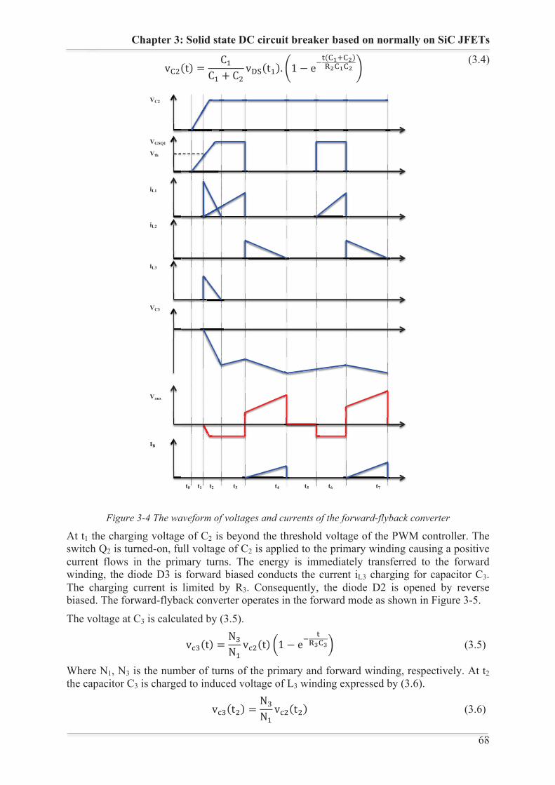
Chapter 3: Solid state DC circuit breaker based on normally on SiC JFETs
68 68
(3.4)
Figure 3-4 The waveform of voltages and currents of the forward-flyback converter
At t1 the charging voltage of C2 is beyond the threshold voltage of the PWM controller. The switch Q2 is turned-on, full voltage of C2 is applied to the primary winding causing a positive current flows in the primary turns. The energy is immediately transferred to the forward winding, the diode D3 is forward biased conducts the current iL3 charging for capacitor C3. The charging current is limited by R3. Consequently, the diode D2 is opened by reverse biased. The forward-flyback converter operates in the forward mode as shown in Figure 3-5.
The voltage at C3 is calculated by (3.5).
(3.5)
Where N1, N3 is the number of turns of the primary and forward winding, respectively. At t2 the capacitor C3 is charged to induced voltage of L3 winding expressed by (3.6).
(3.6)
VC2
VGSQ1
Vth
iL1
iL2
iL3
VC3
Vaux
IB
t0 t1 t2 t3 t4 t5 t6 t7
Chapter 3: Solid state DC circuit breaker based on normally on SiC JFETs
69 69
The JFET is turned off when the voltage of C3 is less than the threshold voltage of JFET. The primary current iL1 comprises the magnetizing current iM and the charging current reflected from the secondary side. The charging current iL3 decreases to zero at t2. The diode D3 does not conduct anymore. From t2 to t3, the Q2 is still on state, but neither of L2 nor L3 conducts current, while the magnetizing current at the primary side continues to ramp up similar to a typical flyback converter, see Figure 3-7. The magnetizing current:
(3.7)
The current flows in the forward winding:
(3.8)
Thus the primary current:
(3.9)
where L1, L3 is the inductance of the primary and forward winding, respectively. At t3, switch Q2 opens, the current no longer has a path through the primary winding. The voltage on L1 is reversed in polarity, which forces the voltage on L2 and L3 to also winding reverse. The diode D2 starts conducting, the D3 blocks. The flyback winding will release energy stored in the transformer during ON period to charge for C3. The current flows into the flyback winding iL2 ramps down to zero because of the applied negative voltage, see Figure 3-7. The forward winding is no longer active due to slight decrease voltage of C2 lead to the induced voltage in L3 winding smaller than the voltage of C3.
The energy stores in the forward-flyback transformer during ON time of Q2 is calculated as follow:
(3.10)
If neglecting the losses, all energy stored in the transformer is used to charge for C3.
(3.11)
And the voltage increased during the flyback mode Vfly can be calculated as (3.12)
(3.12)
The current flow through the flyback winding is:
(3.13)
Therefore the time the magnetizing current following through the flyback winding can be formulated as follow:
(3.14)
On the other hand, input-output relationship of the forward converter is represented by:
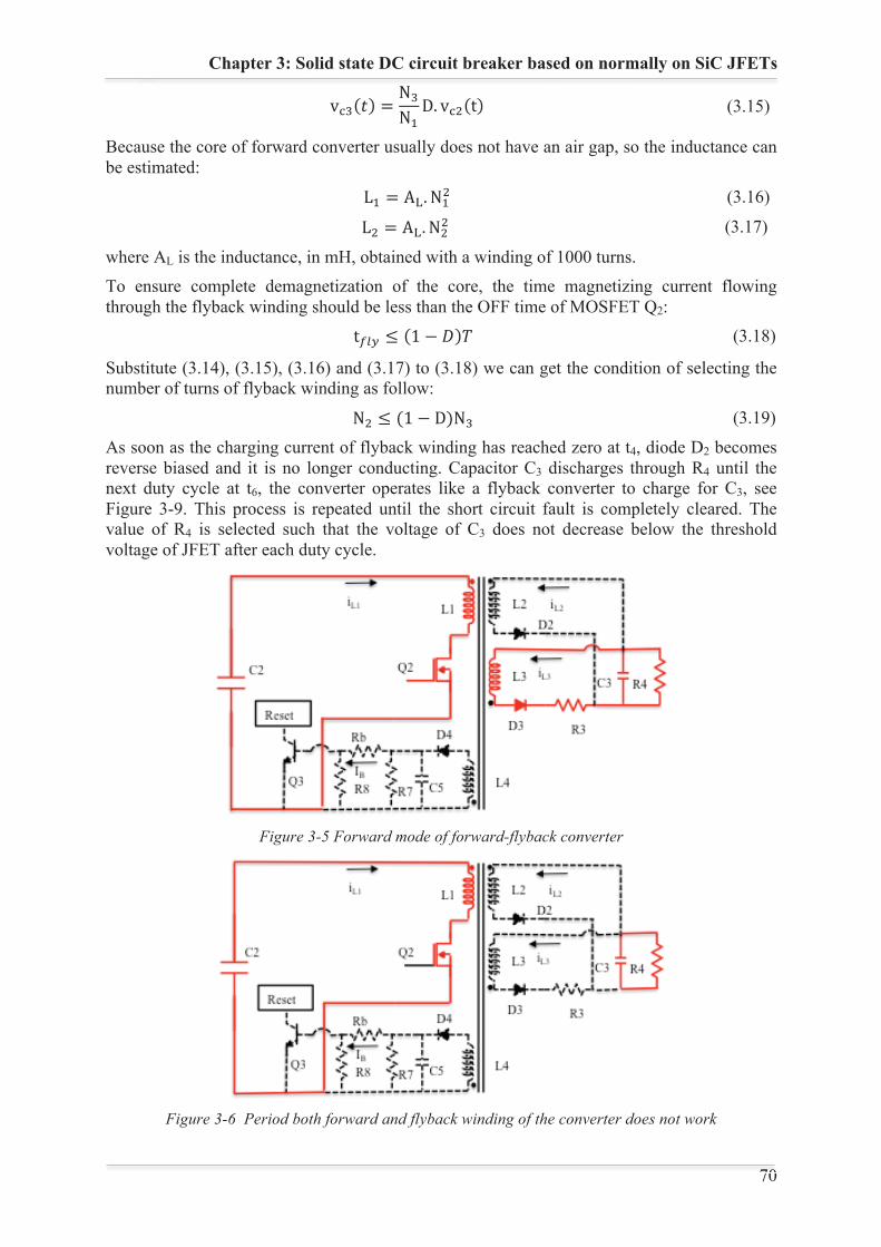
Chapter 3: Solid state DC circuit breaker based on normally on SiC JFETs
70 70
(3.15)
Because the core of forward converter usually does not have an air gap, so the inductance can be estimated:
(3.16)
(3.17)
where AL is the inductance, in mH, obtained with a winding of 1000 turns. To ensure complete demagnetization of the core, the time magnetizing current flowing through the flyback winding should be less than the OFF time of MOSFET Q2:
(3.18)
Substitute (3.14), (3.15), (3.16) and (3.17) to (3.18) we can get the condition of selecting the number of turns of flyback winding as follow:
(3.19)
As soon as the charging current of flyback winding has reached zero at t4, diode D2 becomes reverse biased and it is no longer conducting. Capacitor C3 discharges through R4 until the next duty cycle at t6, the converter operates like a flyback converter to charge for C3, see Figure 3-9. This process is repeated until the short circuit fault is completely cleared. The value of R4 is selected such that the voltage of C3 does not decrease below the threshold voltage of JFET after each duty cycle.
Figure 3-5 Forward mode of forward-flyback converter
Figure 3-6 Period both forward and flyback winding of the converter does not work
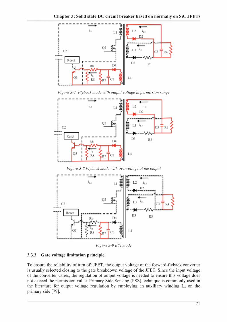
Chapter 3: Solid state DC circuit breaker based on normally on SiC JFETs
71 71
Figure 3-7 Flyback mode with output voltage in permission range
Figure 3-8 Flyback mode with overvoltage at the output
Figure 3-9 Idle mode
3.3.3 Gate voltage limitation principle
To ensure the reliability of turn off JFET, the output voltage of the forward-flyback converter is usually selected closing to the gate breakdown voltage of the JFET. Since the input voltage of the converter varies, the regulation of output voltage is needed to ensure this voltage does not exceed the permission value. Primary Side Sensing (PSS) technique is commonly used in the literature for output voltage regulation by employing an auxiliary winding L4 on the primary side [79].
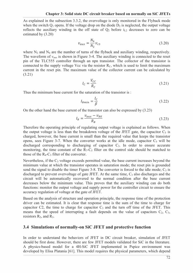
Chapter 3: Solid state DC circuit breaker based on normally on SiC JFETs
72 72
As explained in the subsection 3.3.2, the overvoltage is only monitored in the Flyback mode when the switch Q1 opens. If the voltage drop on the diode D2 is neglected, the output voltage reflects the auxiliary winding in the off state of Q2 before iL2 decreases to zero can be estimated by (3.20)
(3.20)
where N2 and N4 are the number of turns of the flyback and auxiliary winding, respectively. The waveform of vaux is shown in Figure 3-4. The auxiliary winding is connected to the reset pin of the TLC555 controller through an npn transistor. The collector of the transistor is connected to the supply voltage Vcc via the resistor RC, which is used to limit the maximum current in the reset pin. The maximum value of the collector current can be calculated by (3.21)
(3.21)
Thus the minimum base current for the saturation of the transistor is :
(3.22)
On the other hand the base current of the transistor can also be expressed by (3.23)
(3.23)
Therefore the operating principle of regulating output voltage is explained as follows. When the output voltage is less than the breakdown voltage of the JFET gate, the capacitor C5 is charged, however, the base current is small than the required value that keeps the transistor opens, sees Figure 3-7. When the converter works at the idle mode, capacitor C5 will be discharged corresponding to discharging of capacitor C3. In order to ensure accurate monitoring, the time constant of the R7-C5 filter on the control side should be matched to those of the R4-C3 filter of the converter. Nevertheless, if the C3 voltage exceeds permitted value, the base current increases beyond the minimum value at which the transistor operates in saturation mode; the reset pin is grounded send the signal to disable the timer Figure 3-8. The converter is forced to the idle mode; C3 is discharged to prevent overvoltage of gate JFET. At the same time, C3 also discharges and the circuit will be automatically recovered to the normal condition after the base current decreases below the minimum value. This proves that the auxiliary winding can do both functions: monitor the output voltage and supply power for the controller circuit to ensure the accuracy regulation of voltage at the gate of JFET. Based on the analysis of structure and operation principle, the response time of the protection driver can be estimated. It is clear that response time is the sum of the time to charge for capacitor C2, the time to charge for capacitor C3 and the turn off time of the JFET. This means that the speed of interrupting a fault depends on the value of capacitors C2, C3, resistors R2, and R3.
3.4 Simulations of normally-on SiC JFET and protective function
In order to understand the behaviors of JFET in DC circuit breaker, simulation of JFET should be first done. However, there are few JFET models validated for SiC in the literature. A physics-based model for a 4H-SiC JFET implemented in Pspice environment was developed by Elisa Platania [61]. This model requires the physical parameters, which depend
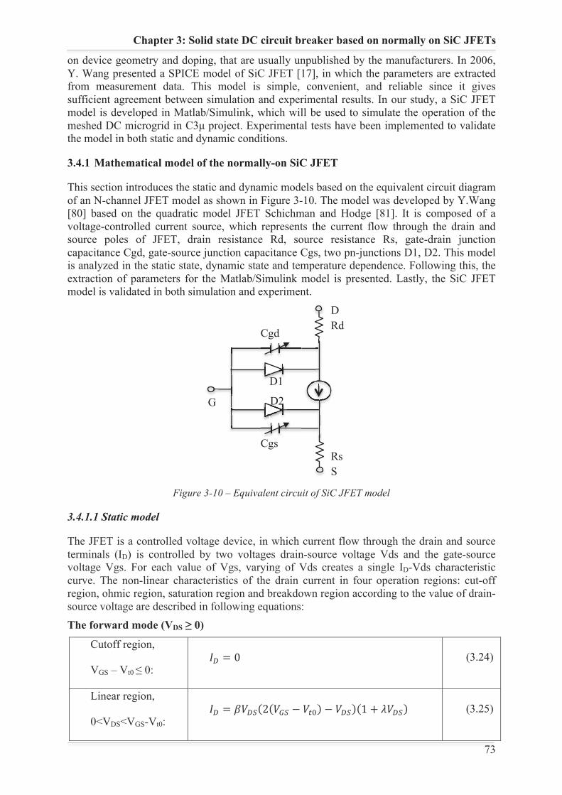
Chapter 3: Solid state DC circuit breaker based on normally on SiC JFETs
73 73
on device geometry and doping, that are usually unpublished by the manufacturers. In 2006, Y. Wang presented a SPICE model of SiC JFET [17], in which the parameters are extracted from measurement data. This model is simple, convenient, and reliable since it gives sufficient agreement between simulation and experimental results. In our study, a SiC JFET model is developed in Matlab/Simulink, which will be used to simulate the operation of the meshed DC microgrid in C3μ project. Experimental tests have been implemented to validate the model in both static and dynamic conditions.
3.4.1 Mathematical model of the normally-on SiC JFET
This section introduces the static and dynamic models based on the equivalent circuit diagram of an N-channel JFET model as shown in Figure 3-10. The model was developed by Y.Wang [80] based on the quadratic model JFET Schichman and Hodge [81]. It is composed of a voltage-controlled current source, which represents the current flow through the drain and source poles of JFET, drain resistance Rd, source resistance Rs, gate-drain junction capacitance Cgd, gate-source junction capacitance Cgs, two pn-junctions D1, D2. This model is analyzed in the static state, dynamic state and temperature dependence. Following this, the extraction of parameters for the Matlab/Simulink model is presented. Lastly, the SiC JFET model is validated in both simulation and experiment.
Figure 3-10 – Equivalent circuit of SiC JFET model
3.4.1.1 Static model
The JFET is a controlled voltage device, in which current flow through the drain and source terminals (ID) is controlled by two voltages drain-source voltage Vds and the gate-source voltage Vgs. For each value of Vgs, varying of Vds creates a single ID-Vds characteristic curve. The non-linear characteristics of the drain current in four operation regions: cut-off region, ohmic region, saturation region and breakdown region according to the value of drain-source voltage are described in following equations: The forward mode (VDS ≥ 0)
Cutoff region,
VGS – Vt0 ≤ 0: (3.24)
Linear region,
0<VDS<VGS-Vt0: (3.25)
D Rd
S Rs
Cgd
G
D1
D2
Cgs
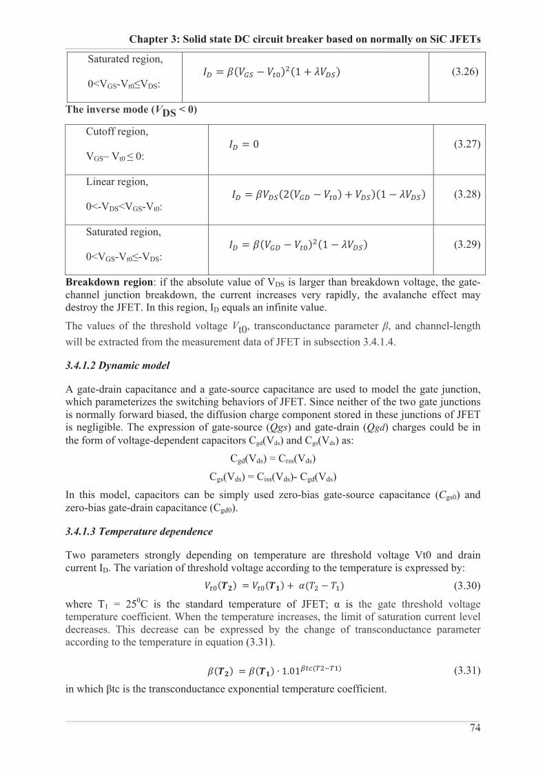
Chapter 3: Solid state DC circuit breaker based on normally on SiC JFETs
74 74
Saturated region,
0<VGS-Vt0≤VDS: (3.26)
The inverse mode (VDS < 0)
Cutoff region,
VGS– Vt0 ≤ 0: (3.27)
Linear region,
0<-VDS<VGS-Vt0: (3.28)
Saturated region,
0<VGS-Vt0≤-VDS: (3.29)
Breakdown region: if the absolute value of VDS is larger than breakdown voltage, the gate-channel junction breakdown, the current increases very rapidly, the avalanche effect may destroy the JFET. In this region, ID equals an infinite value.
The values of the threshold voltage Vt0, transconductance parameter β, and channel-length will be extracted from the measurement data of JFET in subsection 3.4.1.4.
3.4.1.2 Dynamic model
A gate-drain capacitance and a gate-source capacitance are used to model the gate junction, which parameterizes the switching behaviors of JFET. Since neither of the two gate junctions is normally forward biased, the diffusion charge component stored in these junctions of JFET is negligible. The expression of gate-source (Qgs) and gate-drain (Qgd) charges could be in the form of voltage-dependent capacitors Cgd(Vds) and Cgs(Vds) as:
Cgd(Vds) = Crss(Vds)
Cgs(Vds) = Ciss(Vds)- Cgd(Vds) In this model, capacitors can be simply used zero-bias gate-source capacitance (Cgs0) and zero-bias gate-drain capacitance (Cgd0).
3.4.1.3 Temperature dependence
Two parameters strongly depending on temperature are threshold voltage Vt0 and drain current ID. The variation of threshold voltage according to the temperature is expressed by: (3.30)
where T1 = 250C is the standard temperature of JFET; α is the gate threshold voltage temperature coefficient. When the temperature increases, the limit of saturation current level decreases. This decrease can be expressed by the change of transconductance parameter according to the temperature in equation (3.31).
(3.31)
in which βtc is the transconductance exponential temperature coefficient.
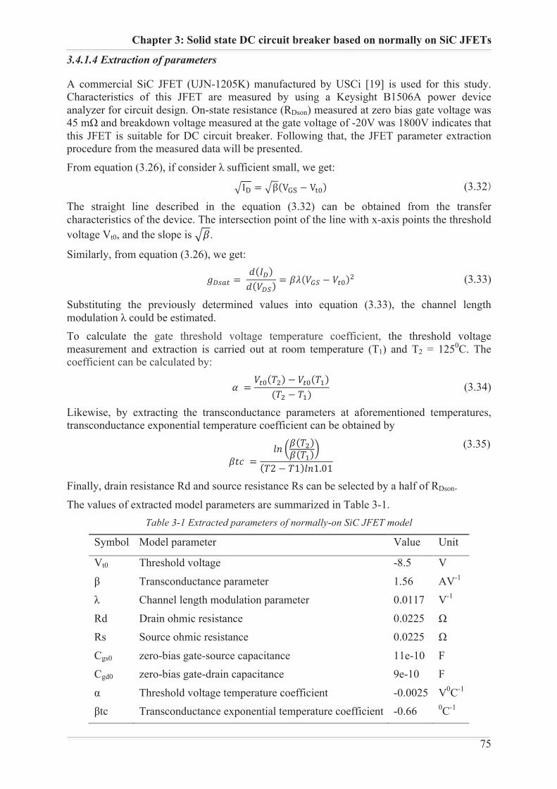
Chapter 3: Solid state DC circuit breaker based on normally on SiC JFETs
75 75
3.4.1.4 Extraction of parameters
A commercial SiC JFET (UJN-1205K) manufactured by USCi [19] is used for this study. Characteristics of this JFET are measured by using a Keysight B1506A power device analyzer for circuit design. On-state resistance (RDson) measured at zero bias gate voltage was 45 mΩ and breakdown voltage measured at the gate voltage of -20V was 1800V indicates that this JFET is suitable for DC circuit breaker. Following that, the JFET parameter extraction procedure from the measured data will be presented.
From equation (3.26), if consider λ sufficient small, we get: (3.32
The straight line described in the equation (3.32) can be obtained from the transfer characteristics of the device. The intersection point of the line with x-axis points the threshold voltage Vt0, and the slope is .
Similarly, from equation (3.26), we get: (3.33)
Substituting the previously determined values into equation (3.33), the channel length modulation λ could be estimated. To calculate the gate threshold voltage temperature coefficient, the threshold voltage measurement and extraction is carried out at room temperature (T1) and T2 = 1250C. The coefficient can be calculated by: (3.34)
Likewise, by extracting the transconductance parameters at aforementioned temperatures, transconductance exponential temperature coefficient can be obtained by
(3.35)
Finally, drain resistance Rd and source resistance Rs can be selected by a half of RDson.
The values of extracted model parameters are summarized in Table 3-1. Table 3-1 Extracted parameters of normally-on SiC JFET model
Symbol Model parameter Value Unit
Vt0 Threshold voltage -8.5 V
β Transconductance parameter 1.56 AV-1
λ Channel length modulation parameter 0.0117 V-1
Rd Drain ohmic resistance 0.0225 Ω Rs Source ohmic resistance 0.0225 Ω
Cgs0 zero-bias gate-source capacitance 11e-10 F Cgd0 zero-bias gate-drain capacitance 9e-10 F
α Threshold voltage temperature coefficient -0.0025 V0C-1
βtc Transconductance exponential temperature coefficient -0.66 0C-1
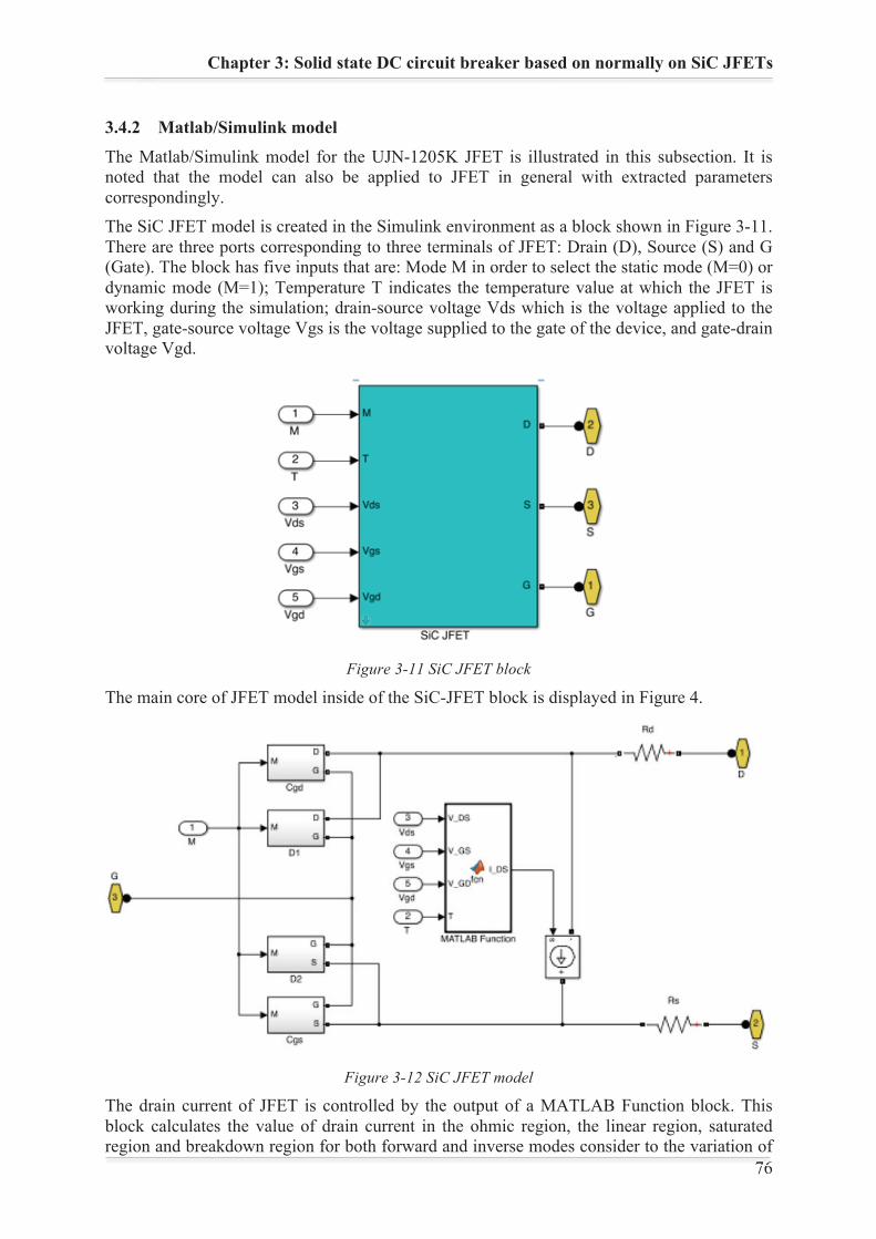
Chapter 3: Solid state DC circuit breaker based on normally on SiC JFETs
76 76
3.4.2 Matlab/Simulink model
The Matlab/Simulink model for the UJN-1205K JFET is illustrated in this subsection. It is noted that the model can also be applied to JFET in general with extracted parameters correspondingly. The SiC JFET model is created in the Simulink environment as a block shown in Figure 3-11. There are three ports corresponding to three terminals of JFET: Drain (D), Source (S) and G (Gate). The block has five inputs that are: Mode M in order to select the static mode (M=0) or dynamic mode (M=1); Temperature T indicates the temperature value at which the JFET is working during the simulation; drain-source voltage Vds which is the voltage applied to the JFET, gate-source voltage Vgs is the voltage supplied to the gate of the device, and gate-drain voltage Vgd.
Figure 3-11 SiC JFET block
The main core of JFET model inside of the SiC-JFET block is displayed in Figure 4.
Figure 3-12 SiC JFET model
The drain current of JFET is controlled by the output of a MATLAB Function block. This block calculates the value of drain current in the ohmic region, the linear region, saturated region and breakdown region for both forward and inverse modes consider to the variation of
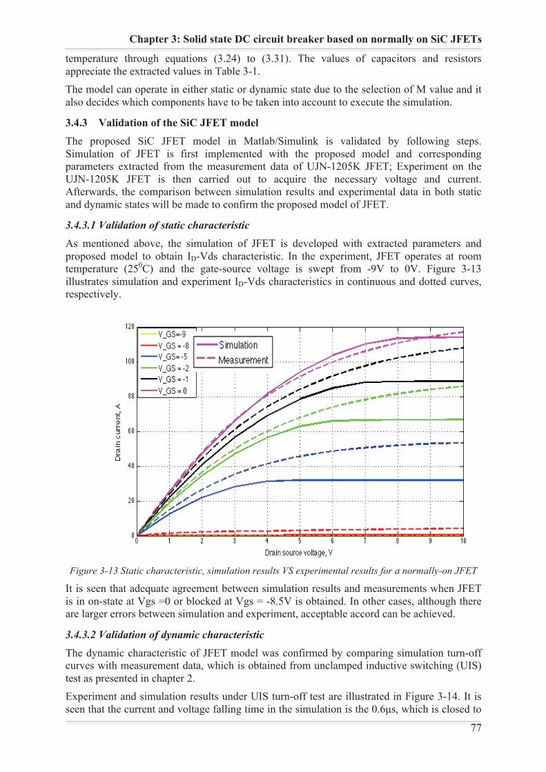
Chapter 3: Solid state DC circuit breaker based on normally on SiC JFETs
77 77
temperature through equations (3.24) to (3.31). The values of capacitors and resistors appreciate the extracted values in Table 3-1. The model can operate in either static or dynamic state due to the selection of M value and it also decides which components have to be taken into account to execute the simulation.
3.4.3 Validation of the SiC JFET model
The proposed SiC JFET model in Matlab/Simulink is validated by following steps. Simulation of JFET is first implemented with the proposed model and corresponding parameters extracted from the measurement data of UJN-1205K JFET; Experiment on the UJN-1205K JFET is then carried out to acquire the necessary voltage and current. Afterwards, the comparison between simulation results and experimental data in both static and dynamic states will be made to confirm the proposed model of JFET.
3.4.3.1 Validation of static characteristic
As mentioned above, the simulation of JFET is developed with extracted parameters and proposed model to obtain ID-Vds characteristic. In the experiment, JFET operates at room temperature (250C) and the gate-source voltage is swept from -9V to 0V. Figure 3-13 illustrates simulation and experiment ID-Vds characteristics in continuous and dotted curves, respectively.
Figure 3-13 Static characteristic, simulation results VS experimental results for a normally-on JFET
It is seen that adequate agreement between simulation results and measurements when JFET is in on-state at Vgs =0 or blocked at Vgs = -8.5V is obtained. In other cases, although there are larger errors between simulation and experiment, acceptable accord can be achieved.
3.4.3.2 Validation of dynamic characteristic
The dynamic characteristic of JFET model was confirmed by comparing simulation turn-off curves with measurement data, which is obtained from unclamped inductive switching (UIS) test as presented in chapter 2. Experiment and simulation results under UIS turn-off test are illustrated in Figure 3-14. It is seen that the current and voltage falling time in the simulation is the 0.6μs, which is closed to
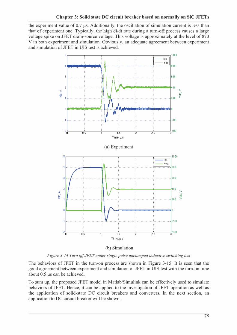
Chapter 3: Solid state DC circuit breaker based on normally on SiC JFETs
78 78
the experiment value of 0.7 μs. Additionally, the oscillation of simulation current is less than that of experiment one. Typically, the high di/dt rate during a turn-off process causes a large voltage spike on JFET drain-source voltage. This voltage is approximately at the level of 870 V in both experiment and simulation. Obviously, an adequate agreement between experiment and simulation of JFET in UIS test is achieved.
(a) Experiment
(b) Simulation
Figure 3-14 Turn off JFET under single pulse unclamped inductive switching test
The behaviors of JFET in the turn-on process are shown in Figure 3-15. It is seen that the good agreement between experiment and simulation of JFET in UIS test with the turn-on time about 0.5 μs can be achieved. To sum up, the proposed JFET model in Matlab/Simulink can be effectively used to simulate behaviors of JFET. Hence, it can be applied to the investigation of JFET operation as well as the application of solid-state DC circuit breakers and converters. In the next section, an application to DC circuit breaker will be shown.
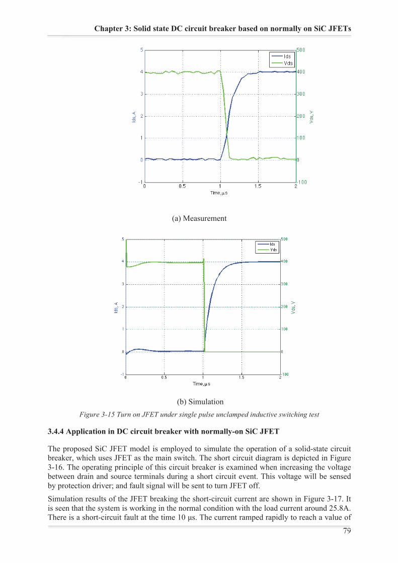
Chapter 3: Solid state DC circuit breaker based on normally on SiC JFETs
79 79
(a) Measurement
(b) Simulation
Figure 3-15 Turn on JFET under single pulse unclamped inductive switching test
3.4.4 Application in DC circuit breaker with normally-on SiC JFET
The proposed SiC JFET model is employed to simulate the operation of a solid-state circuit breaker, which uses JFET as the main switch. The short circuit diagram is depicted in Figure 3-16. The operating principle of this circuit breaker is examined when increasing the voltage between drain and source terminals during a short circuit event. This voltage will be sensed by protection driver; and fault signal will be sent to turn JFET off. Simulation results of the JFET breaking the short-circuit current are shown in Figure 3-17. It is seen that the system is working in the normal condition with the load current around 25.8A. There is a short-circuit fault at the time 10 μs. The current ramped rapidly to reach a value of
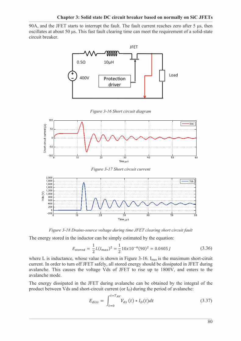
Chapter 3: Solid state DC circuit breaker based on normally on SiC JFETs
80 80
90A, and the JFET starts to interrupt the fault. The fault current reaches zero after 5 μs, then oscillates at about 50 μs. This fast fault clearing time can meet the requirement of a solid-state circuit breaker.
Figure 3-16 Short circuit diagram
Figure 3-17 Short circuit current
Figure 3-18 Drains-source voltage during time JFET clearing short circuit fault
The energy stored in the inductor can be simply estimated by the equation: (3.36)
where L is inductance, whose value is shown in Figure 3-16. Imax is the maximum short-ciruit current. In order to turn off JFET safely, all stored energy should be dissipated in JFET during avalanche. This causes the voltage Vds of JFET to rise up to 1800V, and enters to the avalanche mode. The energy dissipated in the JFET during avalanche can be obtained by the integral of the product between Vds and short-circuit current (or ID) during the period of avalanche:
(3.37)
Chapter 3: Solid state DC circuit breaker based on normally on SiC JFETs
81 81
In the simulation, the dissipated energy in avalanche mode during turn-off of short circuit current is estimated at 0.065J, which is very small in comparison with the JFET critical energy in avalanche mode of 0.65J.
The simulation results illustrate that SSCB will always operate reliability if it can interrupt the short circuit in some microseconds.
3.5 Prototype design of the solid-state circuit breaker based on SiC JFETs
3.5.1 Design of forward-flyback converter for self-powered solid-state circuit breaker
The first step of the designing process a forward-flyback converter concerns clearly defining of design specifications. The parameters, such as input/output voltage, rated power, switching frequency, and duty cycle, need to be identified. After that, the components are selected in order to implement those specifications.
3.5.1.1 Design specifications of the forward-flyback converter
In our study, a 1200 V, 45 mΩ industrial normally-on JFET model UJN 1205K from USCi manufacturer is employed. The parameters of this device were measured and shown in Chapter 2. The specifications to design SSCB have to be compatible with the safety requirements of this JFET. It is clear that the voltage applied to the primary winding of forward-flyback converter is for charging capacitor C2. This voltage is clamped by a 4.7 V Zener diode. On the other hand, the converter will be activated when the voltage of C2 exceeds the threshold voltage of the MOSFET Q2 (around 2 V) and PWM controller (around 3 V to 5 V). So, the maximum input voltage of the converter can be selected at 5 V while the minimum is 3 V.
The output voltage of forward-flyback converter will be applied to the gate of JFET. It should be varied in the range restricted by the gate threshold voltage of the JFET, whose value is - 8.5 V by measurement, and gate the breakdown voltage, which is limited at -20 V. A high switching frequency of 100 kHz is chosen for fast switching and reducing the size of passive devices. In order to ensure completely demagnetization of the core during the flyback mode, a duty cycle of 15 % is chosen.
The power of the converter relates to the maximum current that the gate of JFET can withstand. The forward-flyback converter works as a driver of JFET, which is designed on the basis of the requirement of the power JFET in turning-on and turning-off operation. The speed at which a JFET can be turned on or turned off is related to how fast the gate capacitance of the JFET can be charged and discharged. The relationship between gate capacitance, turn-on/turn-off time and the JFET driver current rating can be written as:
(3.38)
where dT is turn-on/turn-off time, dV is gate voltage, C is gate capacitance (from gate charge value), I is peak drive current (for the given voltage value).The relationship among total gate charge QC, gate capacitance and gate voltage is expressed by
(3.39)
The above equation can be rewritten as:

Chapter 3: Solid state DC circuit breaker based on normally on SiC JFETs
82 82
(3.40)
The value of Q gate charge voltage and turn-on, turn-off time can be referred from the datasheet of JFET.
The estimation of rated power of JFET driver is based on the maximum current allows at the gate JFET. This peak current is generally given for one of two conditions. Either the JFET driver output is shorted to ground or the JFET driver output is at a particular voltage value usually is the gate threshold voltage at which the JFET begins to turn off and the Miller effect comes into play. The peak current rating is also generally stated for the maximum bias voltage of the part. This means if the JFET driver is being used with a lower bias voltage, the peak current drive capability of the JFET driver will be lower. In this case, with the 1200V JFET UJN1205K from USCi datasheet, at threshold voltage Vt0 = -8.5 V, total gate charge Qc = 10nC (Q), rise time/fall time = 28/35 ns the maximum gate current of the JFET at threshold voltage can be calculated:
(3.41)
The output power of forward-flyback converter can be determined as follow: (3.42)
Supposed the efficiency of the forward-flyback converter is 98 %, the input power can be
estimated by:
(3.43)
Thus the forward-flyback converter will be designed with the rated power of 3 W. The specifications for designing of the forward-flyback converter are shown in Table 3-2.
Table 3-2 Specifications to design the forward-flyback converter
Symbol Parameters Value Unit
Vinmax Maximum input voltage 5 V
Vinmin Minimum input voltage 3 V
Voutmin Minimum output voltage -20 V
Voutmax Maximum output voltage -8.5 V
P Rated power 3 W
fsw Switching frequency 100 kHz
D Duty cycle 15 %
3.5.1.2 Design of forward-flyback transformer
The forward-flyback transformer plays an important role in the forward-flyback converter. It is used for coupling between the primary winding and two secondary windings, and between flyback winding and the auxiliary winding. The transformer design in this thesis based on the area product method that was presented in [82], [83]. In the literature, the core used for the transformer can be made with different shapes and sizes, and from various materials. However, at the high switching frequency, the ferrite material is preferred since it provides a reduction of core losses. On the other hand to reduce the number of turns of windings and

Chapter 3: Solid state DC circuit breaker based on normally on SiC JFETs
83 83
obtain higher leakage inductance, the materials with medium to high permeability a selected. The ferrite provides medium initial permeability of 0.1 to 0.5 Tesla. Reference to the specifications of core manufacturers the N87 is the best material for designing the transformer. For forward-mode applications, no gap is required. The core product area (AP), which is the core magnetic cross-section area (Ae) multiplied by window area available for winding (AW), is widely used for an initial estimation of the core size for a given switching frequency:
(3.44)
where
= 4 is coefficient of the square waveform.
is the allowed maximum flux density in normal operation which is usually preset to be the saturation flux density of the core material, choose Bmax = 0.1 T.
is the window utilization factor, typically 0.4
is the constant current density. i= 468.
χ is an exponent regards to the core form, χ = 1.16
(3.45)
The core EFD 30/15/9 made of N87 material manufacturer from ESCO is the selection. Where, the effective core area: Ae = 69 mm2, window area: AW = 52.3 mm2, path length le = 68mm. With a given core size, there is a minimum number of turns for the transformer primary side winding to avoid saturation.
(3.46)
Select the number of turns of primary winding N1 = 5 turns.
Based on (3.6), (3.19), and (3.20) equations, we can estimate the number of turns of forward winding, flyback winding and auxiliary winding are 20, 16, and 4 turns, respectively.
The parameters of the forward flyback transformer are shown in Table 3-3. The output capacitor is calculated by:
(3.47)
where is the output ripple voltage, chosen equal to 5% of output voltage.
(3.48)
∆Iout is the peak-to-peak ripple current in the output, typically equal to 20% of the maximum load current.
(3.49)
Thus

Chapter 3: Solid state DC circuit breaker based on normally on SiC JFETs
84 84
(3.50)
Table 3-3 Designed parameters of forward-flyback transformer
Symbol Parameters Value Unit
N1 Number of turns of the primary winding 5
N2 Number of turns of the flyback winding 16
N3 Number of turns of the forward winding 20
N4 Number of turns of the auxiliary winding 4
L1 Magnetizing inductance (Primary) 51 μH
L2 Magnetizing inductance (flyback) 524 μH
L3 Magnetizing inductance (forward) 820 μH
L4 Magnetizing inductance (auxiliary) 32 μH
A resistor (R3) of 56 Ω is connected in series with C3 in order to reduce the charging current during the forward mode of the transformer. Resistor R4 equal to 22 kΩ in order to ensure keep sufficient time for completely turn off JFET. The selection of the MOSFET switch (Q2) should be done analyzing the maximum voltage it has to withstand and fast startup. During TON the voltage on the switch is almost zero since the switch is closed. While in the flyback mode, it has to sustain the total of the voltage applied to the primary and reflect voltage from secondary. The MOSFET IRL530N from International Rectifier, with VDS = 100 V, IDS = 36 A, threshold voltage of 2 V is selected. A power MOSFET driver TC 4428 is employed in order to increase the current applied to the gate of Q2 for increasing the speed of starting Q2.
A low power consumption, low starting voltage, reliable IC controller model TLC 555 (CMOS technology) from Texas Instrument is employed to control the operation of MOSFET Q2. The switching frequency and duty cycle are adjusted by controlling the value of resistors R5, R6 and C4. Its reset pin is connected to the adjusted output voltage circuitry to interrupt the Q2 if the output voltage exceeds the permitted value. A MOV model 20D43K with rating power of 430 V and maximum clamping voltage of 710 V is chosen for preventing overvoltage of drain-source when JFET is opened.
3.5.2 Selection of components of voltage sensor
The operating principle of voltage sensor circuit can be divided into two stages with different functions as described above. At the first stage, when short circuit even occurs, the voltage sensor charge for both C1 and C2 through R2, until C2 is fully charged. The capacitor C2 should have small value in comparison with C1, thus almost voltage will be charged for C2. After C2 is fully charged, the current is no longer flow through the C2, capacitor C1 has to maintain charging in order to supply current enough for the operation of the forward-flyback converter. Therefore, the total time constant of charging both C2 and C1 should be higher the charging time of output capacitor C3 to ensure JFET totally turns off. So resistor R2 is selected equal to 1 Ω, while capacitor C1 and C2 are 1 μF and 10 nF, respectively. On the other time, after JFET opened, the bus voltage of 400 V is applied to the voltage sensor, a small current will flow through resistor R1 to maintain the clamping voltage of the
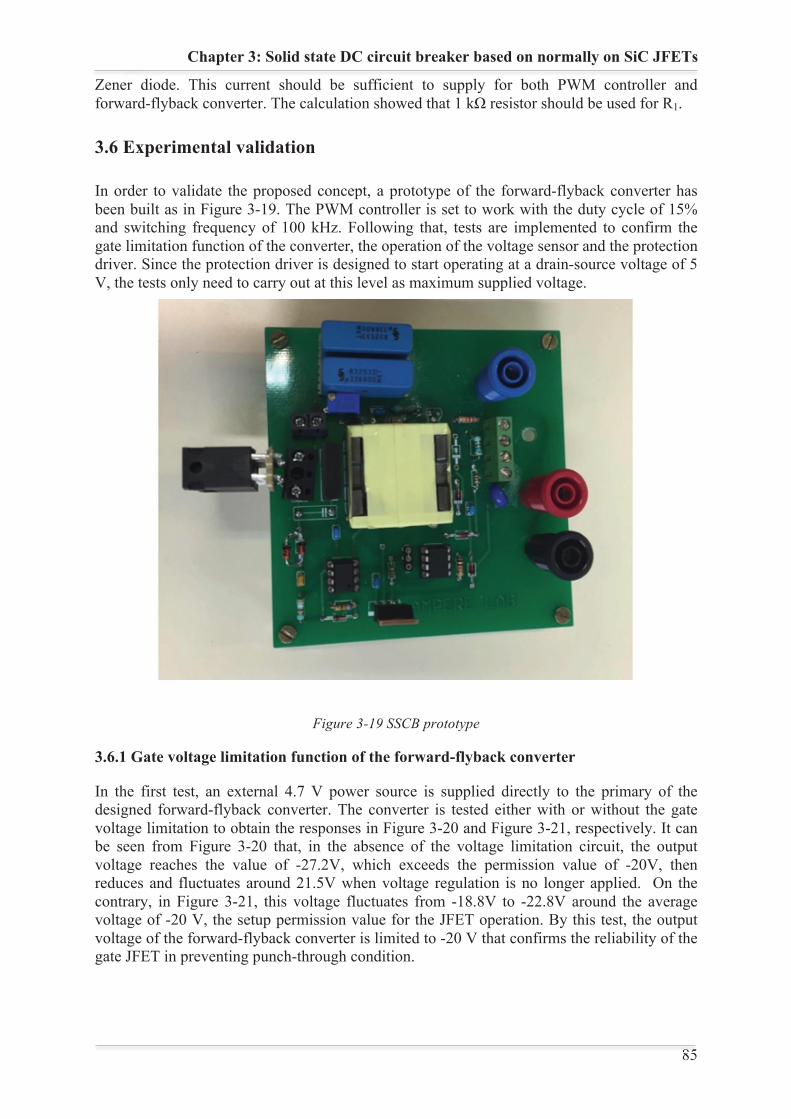
Chapter 3: Solid state DC circuit breaker based on normally on SiC JFETs
85 85
Zener diode. This current should be sufficient to supply for both PWM controller and forward-flyback converter. The calculation showed that 1 kΩ resistor should be used for R1.
3.6 Experimental validation
In order to validate the proposed concept, a prototype of the forward-flyback converter has been built as in Figure 3-19. The PWM controller is set to work with the duty cycle of 15% and switching frequency of 100 kHz. Following that, tests are implemented to confirm the gate limitation function of the converter, the operation of the voltage sensor and the protection driver. Since the protection driver is designed to start operating at a drain-source voltage of 5 V, the tests only need to carry out at this level as maximum supplied voltage.
Figure 3-19 SSCB prototype
3.6.1 Gate voltage limitation function of the forward-flyback converter
In the first test, an external 4.7 V power source is supplied directly to the primary of the designed forward-flyback converter. The converter is tested either with or without the gate voltage limitation to obtain the responses in Figure 3-20 and Figure 3-21, respectively. It can be seen from Figure 3-20 that, in the absence of the voltage limitation circuit, the output voltage reaches the value of -27.2V, which exceeds the permission value of -20V, then reduces and fluctuates around 21.5V when voltage regulation is no longer applied. On the contrary, in Figure 3-21, this voltage fluctuates from -18.8V to -22.8V around the average voltage of -20 V, the setup permission value for the JFET operation. By this test, the output voltage of the forward-flyback converter is limited to -20 V that confirms the reliability of the gate JFET in preventing punch-through condition.
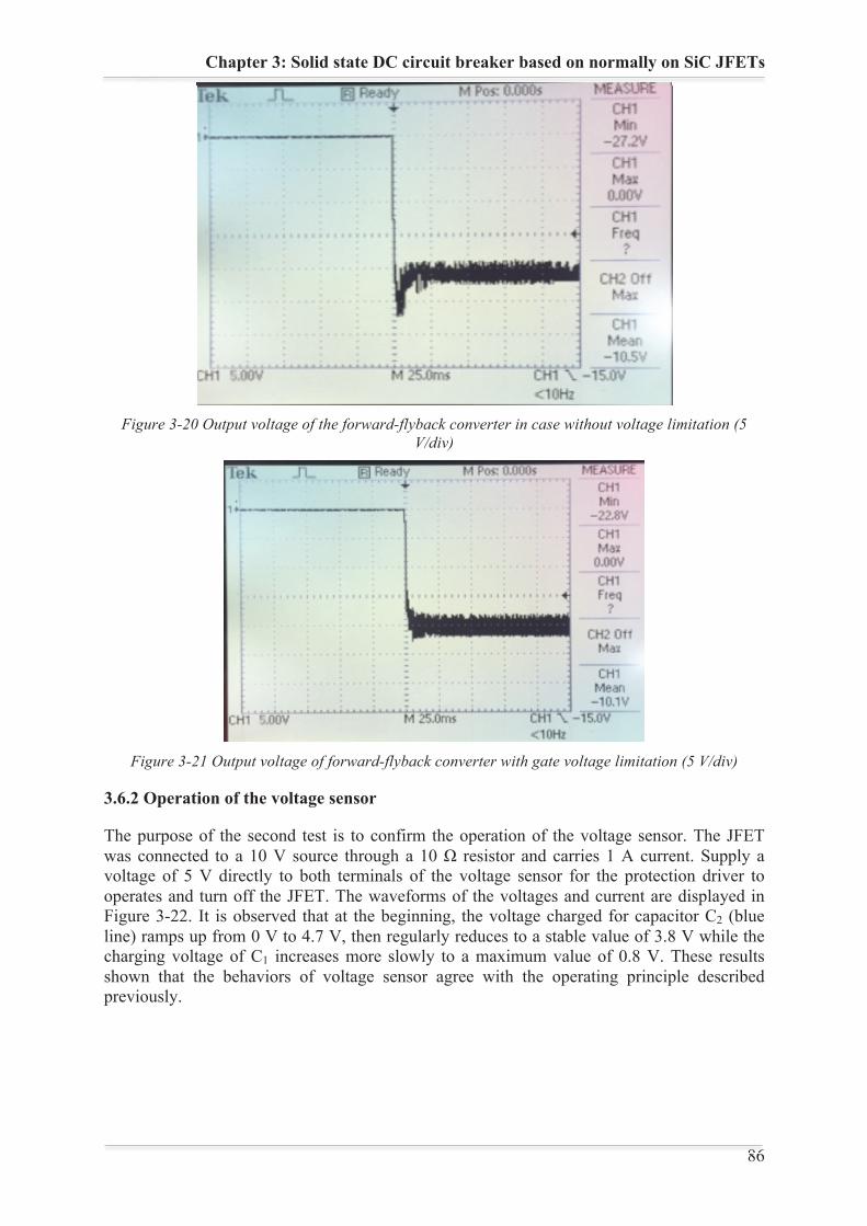
Chapter 3: Solid state DC circuit breaker based on normally on SiC JFETs
86 86
Figure 3-20 Output voltage of the forward-flyback converter in case without voltage limitation (5
V/div)
Figure 3-21 Output voltage of forward-flyback converter with gate voltage limitation (5 V/div)
3.6.2 Operation of the voltage sensor
The purpose of the second test is to confirm the operation of the voltage sensor. The JFET was connected to a 10 V source through a 10 Ω resistor and carries 1 A current. Supply a voltage of 5 V directly to both terminals of the voltage sensor for the protection driver to operates and turn off the JFET. The waveforms of the voltages and current are displayed in Figure 3-22. It is observed that at the beginning, the voltage charged for capacitor C2 (blue line) ramps up from 0 V to 4.7 V, then regularly reduces to a stable value of 3.8 V while the charging voltage of C1 increases more slowly to a maximum value of 0.8 V. These results shown that the behaviors of voltage sensor agree with the operating principle described previously.
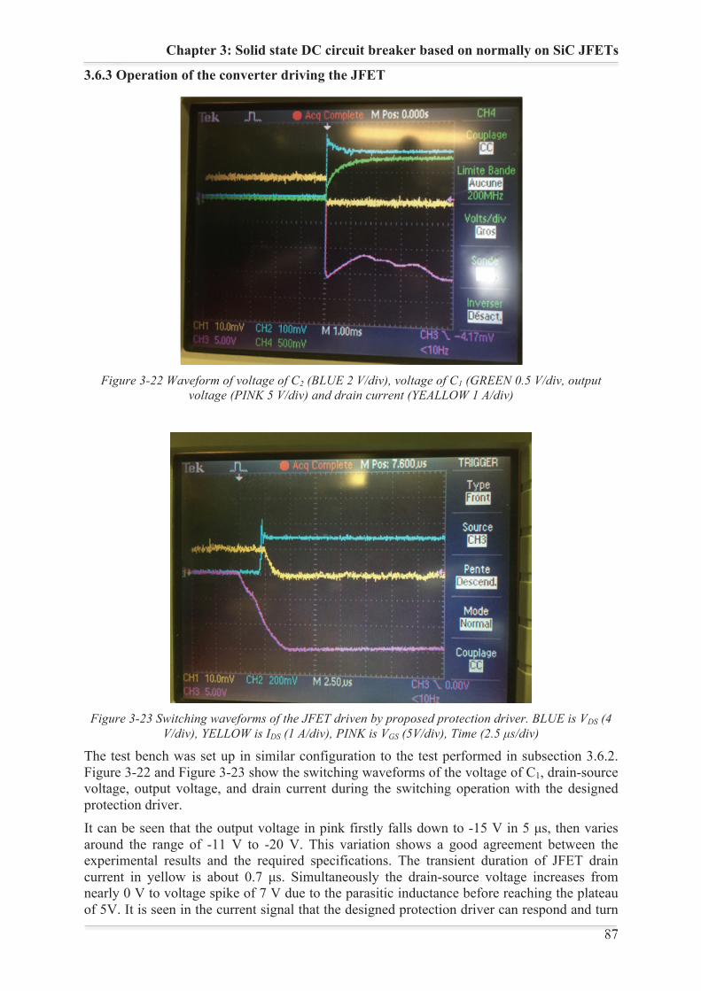
Chapter 3: Solid state DC circuit breaker based on normally on SiC JFETs
87 87
3.6.3 Operation of the converter driving the JFET
Figure 3-22 Waveform of voltage of C2 (BLUE 2 V/div), voltage of C1 (GREEN 0.5 V/div, output
voltage (PINK 5 V/div) and drain current (YEALLOW 1 A/div)
Figure 3-23 Switching waveforms of the JFET driven by proposed protection driver. BLUE is VDS (4
V/div), YELLOW is IDS (1 A/div), PINK is VGS (5V/div), Time (2.5 μs/div)
The test bench was set up in similar configuration to the test performed in subsection 3.6.2. Figure 3-22 and Figure 3-23 show the switching waveforms of the voltage of C1, drain-source voltage, output voltage, and drain current during the switching operation with the designed protection driver. It can be seen that the output voltage in pink firstly falls down to -15 V in 5 μs, then varies around the range of -11 V to -20 V. This variation shows a good agreement between the experimental results and the required specifications. The transient duration of JFET drain current in yellow is about 0.7 μs. Simultaneously the drain-source voltage increases from nearly 0 V to voltage spike of 7 V due to the parasitic inductance before reaching the plateau of 5V. It is seen in the current signal that the designed protection driver can respond and turn
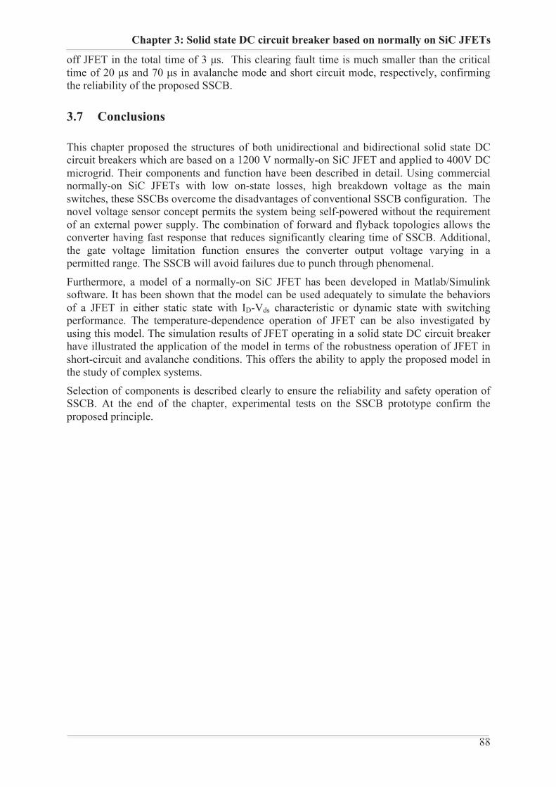
Chapter 3: Solid state DC circuit breaker based on normally on SiC JFETs
88 88
off JFET in the total time of 3 μs. This clearing fault time is much smaller than the critical time of 20 μs and 70 μs in avalanche mode and short circuit mode, respectively, confirming the reliability of the proposed SSCB.
3.7 Conclusions
This chapter proposed the structures of both unidirectional and bidirectional solid state DC circuit breakers which are based on a 1200 V normally-on SiC JFET and applied to 400V DC microgrid. Their components and function have been described in detail. Using commercial normally-on SiC JFETs with low on-state losses, high breakdown voltage as the main switches, these SSCBs overcome the disadvantages of conventional SSCB configuration. The novel voltage sensor concept permits the system being self-powered without the requirement of an external power supply. The combination of forward and flyback topologies allows the converter having fast response that reduces significantly clearing time of SSCB. Additional, the gate voltage limitation function ensures the converter output voltage varying in a permitted range. The SSCB will avoid failures due to punch through phenomenal.
Furthermore, a model of a normally-on SiC JFET has been developed in Matlab/Simulink software. It has been shown that the model can be used adequately to simulate the behaviors of a JFET in either static state with ID-Vds characteristic or dynamic state with switching performance. The temperature-dependence operation of JFET can be also investigated by using this model. The simulation results of JFET operating in a solid state DC circuit breaker have illustrated the application of the model in terms of the robustness operation of JFET in short-circuit and avalanche conditions. This offers the ability to apply the proposed model in the study of complex systems.
Selection of components is described clearly to ensure the reliability and safety operation of SSCB. At the end of the chapter, experimental tests on the SSCB prototype confirm the proposed principle.
Conclusions and Perspectives
89 89
CONCLUSIONS AND PERSPECTIVES
Conclusions
Regarding the policies encouraging energy efficiency, the growing of DC loads and the deeper application of distributed sources result in the applicability of DC microgrid in the domestic area. One of the challenges to the development of DC microgrid is overcurrent protection due to high value and high rate of rise of the short circuit current. Power electronic circuit breaker is considered as a solution replacing for the common mechanical circuit breaker.
The comparison of some solid state circuit breaker topologies indicates the advantages of self-power concept which detects the fault based on the drop voltage in the semiconductor device and supplies power for protection driver without the requirement of external power source. The semiconductor is the most important device in the SSCB. Typical semiconductor devices, such as Si IGBTs, Si MOSFETs, SiC MOSFETs, SiC BJTs, and SiC JFETs, were analyzed; and the results showed that the normally-on SiC JFET is the most suitable device for SSCB applications due to the superiorities in low on-state resistance, high breakdown voltage and robustness with the short circuit.
A commercial normally-on SiC JFET from USCi was chosen for investigation. Experimental tests were carried out in order to identify the parameters of the JFET, which are used to estimate specifications of the SSCB. For more detail, based on the static characteristics of the JFET and the desired current limiting, the stating voltage of the protection driver is defined. Output of protection driver is identified on the basis of the permitted range voltage of the gate of JFET (in range of threshold voltage and gate breakdown voltage). The dynamic and switching characteristics were also analyzed. In particular, the robustness of the selected JFET is investigated precisely in order to identify the limit of destructing the devices. The experimental results show the great robustness of the normally-on JFET with the critical energy in short circuit mode at the voltage of 400 V is about 1.9 J corresponding to short circuit withstand time of 70 μs. The normally-on JFET is realized with easier failure in avalanche mode than that of short circuit mode. The maximum dissipated energy the normally-on JFET could withstand without failure is 0.65 J, corresponding to the withstand time of 20 μs. However, this issue can be solved using a MOV, which is connected across to the JFET in order to clamp the voltage under the breakdown voltage when JFET is opened. In addition, the normally-on characteristic, which seems to bring the drawback of JFET in converter application, becomes an advantage in SSCB application. The protection driver will not have to operate in the normal condition, but the short circuit event.
Based on the analyzed characteristics of the normally-on SiC JFET, two solid-state DC circuit breaker topologies corresponding to uni-direction and bi-direction are proposed. The design of SSCB aims to two objectives: fast response time and reliability. For what, an SSCB comprised of one or two normally-on SiC JFET/JFETs act as the main switching device. The switch is controlled by a protection driver. The third part is a MOV used to limit the transient voltage during the opening process of the JFET. The protection driver consists of a voltage sensor and an ultra-fast DC-DC converter. The voltage sensor detects the fault and sends the signal to activate the converter. Furthermore, it also supplies a DC power source in order to maintain the operation of the converter during clearing fault duration with no extra power supply requirement. The combination of both forward and flyback topologies in the DC-DC converter promotes the advantage of directly transfer while ensuring demagnetization of the core and add more voltage to the output. The gate driver based on this forward-flyback converter reduces significantly the response time of the driver. Moreover, the reliability of the
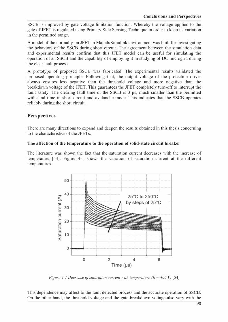
Conclusions and Perspectives
90 90
SSCB is improved by gate voltage limitation function. Whereby the voltage applied to the gate of JFET is regulated using Primary Side Sensing Technique in order to keep its variation in the permitted range.
A model of the normally-on JFET in Matlab/Simulink environment was built for investigating the behaviors of the SSCB during short circuit. The agreement between the simulation data and experimental results confirm that this JFET model can be useful for simulating the operation of an SSCB and the capability of employing it in studying of DC microgrid during the clear fault process. A prototype of proposed SSCB was fabricated. The experimental results validated the proposed operating principle. Following that, the output voltage of the protection driver always ensures less negative than the threshold voltage and more negative than the breakdown voltage of the JFET. This guarantees the JFET completely turn-off to interrupt the fault safely. The clearing fault time of the SSCB is 3 μs, much smaller than the permitted withstand time in short circuit and avalanche mode. This indicates that the SSCB operates reliably during the short circuit.
Perspectives
There are many directions to expand and deepen the results obtained in this thesis concerning to the characteristics of the JFETs.
The affection of the temperature to the operation of solid-state circuit breaker
The literature was shown the fact that the saturation current decreases with the increase of temperature [54]. Figure 4-1 shows the variation of saturation current at the different temperatures.
Figure 4-1 Decrease of saturation current with temperature (E = 400 V) [54]
This dependence may affect to the fault detected process and the accurate operation of SSCB. On the other hand, the threshold voltage and the gate breakdown voltage also vary with the
Conclusions and Perspectives
91 91
change of temperature [78], [84]. The papers reported that the gate to source range allowed to block the JFET reduce when the temperature increases may result in failure due to gate punch-through phenomenon.
Challenges regarding parallel connection of SiC JFETs.
Each JFET component has a limited rating current of 38 A that is not sufficient to high power applications. In order to improve the rating of the devices, several JFETs can be connected in parallel. In [85], [86], the challenges concerning to the connection of several JFET in parallel in the converter were investigated. Whereby, the threshold voltage and gate breakdown voltage are the most crucial parameters affecting the operation of the parallel JFETs. Investigation showed that even if the two JFETs have the similar breakdown voltage, their switching performances are not exactly the same. Furthermore, the variation in the on-state resistance and static transfer characteristic of the SiC JFETs might also affect the switching transient of themselves. In SSCB, the JFETs have to operate at very high current value therefore if they do not turn off at the same time, the failures may occur.
92 92
PUBLICATIONS
During the thesis, the following publications have been realized: {1} T. T. H. Ma, T. K. Tran, H. Yahoui, N. Siauve, H. G. Vu, Design of a Forward-Flyback Converter Based Drive with Gate Voltage Limitation for a DC Circuit Breaker Using Normally-on SiC JFET, The 2nd IEEE International Conference on DC Microgrids, Nurnberg, Germany, 27-29 June 2017. {2} T. T. H. Ma, H. Yahoui, H. G. Vu, N. Siauve, H. Morel, A Control Strategy of DC Building Microgrid Connected to the Neighborhood and AC Power Network, Buildings, 7(2), 42, doi:10.3390/buildings7020042, 2017.
{3} T. T. H. Ma, H. Yahoui, F. B. E. Boubkari, H. Morel, H. G. Vu and N. Siauve, Building a Matlab/Simulink Model of SiC JFET for the investigation of Solid State DC Breaker, International Conference on Components and Systems for DC Grids, Grenoble, France, 14 - 15 March 2017.
{4} Thanh-Kha Tran, Thi Thuong Huyen Ma, Hamed Yahoui, Nicolas Siauve, Y Ouldboukhitine, Simulation of the photovoltaic using Zeta Converter with Battery storage system for lighting at night in decentralised areas, Second International Workshop on Sustainability and Resilience of Bio-energy for Climate Change: Scoping and Envisioning, Mar 2017, Danang, Vietnam. 2017. {5} Hamed Yahoui, Thi Thuong Huyen Ma, Hoang-Giang Vu, Nicolas Siauve. Knowledge, skills and competences for green sustainable energy systems requirement, International Workshop on Sustainability and Resilience of Bio-energy for Climate Change: Scoping and Envisioning, May 2016, Bali, Indonesia. 2016. {6} VU Hoang Giang, MA Thi Thuong Huyen, Investigation and simulating of the photovoltaic system connected to power grid via a three-phase voltage source inverter, EPU Journal of Sience and Technology for Energy, Vietnam no.10, pp.9-14, Mar. 2016.
93 93
BIBLIOGRAPHY
[1] ODYSSEE-MURE, “Energy Efficiency Trends and Policies in the Household and Tertiary Sectors,” ADEME, 2015.
Available: http://www.odyssee-mure.eu/ publications/br/energy-efficiency-trends-policies- buildings.pdf.
[2] P. Bertoldi, B. Hirl, and N. Labanca, "Energy Efficiency Status Report on Electricity Consumption and Efficiency Trends in the European Union," status report 2012, European Commission Joint Research Centre, Institute for Energy, Luxembourg, 2012.
[3] P. Torcellini, S. Pless, and M. Deru, “Zero Energy Buildings : A Critical Look at the Definition Preprint,” ACEEE Summer study, vol. 2, p. 15, 2006.
[4] K. Garbesi, V. Vossos, and H. Shen, “Catalog of DC Appliances and Power Systems,” Lawrence Berkeley National Laboratory, Berkeley, CA (United States), 2010.
[5] J. M. Guerrero, J. C. Vasquez, J. Matas, L. G. De Vicuña, and M. Castilla, “Hierarchical control of droop-controlled AC and DC microgrids - A general approach toward standardization,” IEEE Trans. Ind. Electron., vol. 58, no. 1, pp. 158–172, 2011.
[6] M. Sechilariu, B. Wang, and F. Locment, “Power management and optimization for isolated DC microgrid,” in 2014 International Symposium on Power Electronics, Electrical Drives, Automation and Motion, pp. 1284–1289, 2014.
[7] L. Che and M. Shahidehpour, “DC microgrids: Economic operation and enhancement of resilience by hierarchical control,” IEEE Trans. Smart Grid, vol. 5, no. 5, pp. 2517–2526, 2014.
[8] W. Chen, X. Zhu, L. Yao, G. Ning, Y. Li, Z. Wang, W. Gu, and X. Qu, “A Novel Interline DC Power-Flow Controller (IDCPFC) for Meshed HVDC Grids,” IEEE Trans. Power Deliv., vol. 31, no. 4, pp. 1719–1727, 2016.
[9] Y. Ito, Y. Zhongqing, and H. Akagi, “DC microgrid based distribution power generation system,” IEEE 4th Int. Power Electronics and Motion Control Conf. (IPEMC), vol. 3, pp. 1740–1745, Aug.2004.
[10] A. Kwasinski and P. T. Krein, “A Microgrid-based Telecom Power System using Modular Multiple-Input DC-DC Converters,” in INTELEC 05 Twenty-Seventh International Telecommunications Conference, pp. 515–520, 2005.
[11] H. Kakigano, Y. Miura, T. Ise, and R. Uchida, “DC micro-grid for super high quality distribution; System configuration and control of distributed generations and energy storage devices,” in 2006 37th IEEE Power Electronics Specialists Conference, pp. 1–7, 2006.
[12] D. Salomonsson, L. Soder, and A. Sannino, “An Adaptive Control System for a DC Microgrid for Data Centers,” IEEE Trans. Ind. Appl., vol. 44, no. 6, pp. 1910–1917, 2008.
94 94
[13] T. Dragicevic, J. C. Vasquez, J. M. Guerrero, and D. Skrlec, “Advanced LVDC Electrical Power Architectures and Microgrids: A step toward a new generation of power distribution networks.,” IEEE Electrif. Mag., vol. 2, no. 1, pp. 54–65, 2014.
[14] D. Dong, I. Cvetkovic, D. Boroyevich, W. Zhang, R. Wang, and P. Mattavelli, “Grid-Interface Bidirectional Converter for Residential DC Distribution Systems;Part One: High-Density Two-Stage Topology,” IEEE Trans. Power Electron., vol. 28, no. 4, pp. 1655–1666, 2013.
[15] M. Sechilariu, F. Locment, and I. Houssamo, “Multi-source power generation system in semi-isolated and safety grid configuration for buildings,” in Melecon 2010 - 2010 15th IEEE Mediterranean Electrotechnical Conference, pp. 967–972, 2010.
[16] M. Sechilariu, B. Wang, and F. Locment, “Building Integrated Photovoltaic System With Energy Storage and Smart Grid Communication,” IEEE Trans. Ind. Electron., vol. 60, no. 4, pp. 1607–1618, 2013.
[17] B. Wang, M. Sechilariu, and F. Locment, “Intelligent DC Microgrid With Smart Grid Communications: Control Strategy Consideration and Design,” IEEE Trans. Smart Grid, vol. 3, no. 4, pp. 2148–2156, 2012.
[18] S. Jung, H. Lee, C. S. Song, J. H. Han, W. K. Han, and G. Jang, “Optimal Operation Plan of the Online Electric Vehicle System Through Establishment of a DC Distribution System,” IEEE Trans. Power Electron., vol. 28, no. 12, pp. 5878–5889, 2013.
[19] S. Rivera, B. Wu, S. Kouro, V. Yaramasu, and J. Wang, “Electric Vehicle Charging Station Using a Neutral Point Clamped Converter With Bipolar DC Bus,” IEEE Trans. Ind. Electron., vol. 62, no. 4, pp. 1999–2009, 2015.
[20] H. Zhou, T. Bhattacharya, D. Tran, T. S. T. Siew, and A. M. Khambadkone, “Composite Energy Storage System Involving Battery and Ultracapacitor With Dynamic Energy Management in Microgrid Applications,” IEEE Trans. Power Electron., vol. 26, no. 3, pp. 923–930, 2011.
[21] T. Dragicevic, X. Lu, J. C. Vasquez, and J. M. Guerrero, “DC Microgrids - Part I: A Review of Control Strategies and Stabilization Techniques,” IEEE Trans. Power Electron., vol. 31, no. 7, pp. 4876–4891, 2016.
[22] T. Dragičević, X. Lu, J. C. Vasquez, and J. M. Guerrero, “DC Microgrids - Part II: A Review of Power Architectures, Applications, and Standardization Issues,” IEEE Trans. Power Electron., vol. 31, no. 5, pp. 3528–3549, 2016.
[23] N. Hatziargyriou, H. Asano, R. Iravani, and C. Marnay, “Microgrids,” IEEE Power Energy Mag., vol. 5, no. 4, pp. 78–94, Jul. 2007.
[24] E. Rodriguez-Diaz, M. Savaghebi, J. C. Vasquez, and J. M. Guerrero, “An overview of low voltage DC distribution systems for residential applications,” 5th IEEE Int. Conf. Consum. Electron. - Berlin, ICCE-Berlin 2015, pp. 318–322, 2016.
95 95
[25] S. Moayedi and A. Davoudi, “Cooperative power management in DC microgrid clusters,” 2015 IEEE 1st Int. Conf. Direct Curr. Microgrids, ICDCM 2015, pp. 75–80, 2015.
[26] J. D. Park, J. Candelaria, L. Ma, and K. Dunn, “DC Ring-Bus Microgrid Fault Protection and Identification of Fault Location,” IEEE Trans. Power Deliv., vol. 28, no. 4, pp. 2574–2584, 2013.
[27] L. Mackay, T. Hailu, L. Ramirez-Elizondo, and P. Bauer, “Decentralized current limiting in meshed DC distribution grids,” 2015 IEEE 1st Int. Conf. Direct Curr. Microgrids, ICDCM 2015, pp. 234–238, 2015.
[28] J. D. Park and J. Candelaria, “Fault Detection and Isolation in Low-Voltage DC-Bus Microgrid System,” IEEE Trans. Power Deliv., vol. 28, no. 2, pp. 779–787, 2013.
[29] D. Salomonsson, L. Soder, and A. Sannino, “Protection of Low-Voltage DC Microgrids,” IEEE Trans. Power Deliv., vol. 24, no. 3, pp. 1045–1053, 2009.
[30] J. Yang, J. E. Fletcher, and J. O’Reilly, “Short-Circuit and Ground Fault Analyses and Location in VSC-Based DC Network Cables,” IEEE Trans. Ind. Electron., vol. 59, no. 10, pp. 3827–3837, 2012.
[31] A. Berizzi, A. Silvestri, D. Zaninelli, and S. Massucco, “Shot circuit curent calculations for DC systems,” IEEE Trans. Ind. Appl.,vol. 32, no. 5, pp. 990–997, 1996.
[32] ABB, “ABB Circuit breakers for direct current applications,” Technical application papers, 2007.
[33] W. Y. Kong, “Review of DC Circuit Breakers for Submarine Applications,” The Defence Science and Technology Organisation, Tech. Rep., 2012.
[34] IEEE, "IEEE Guide for the Protection of Stationary Battery Systems," IEEE 1375. New York, NY, USA, 1998.
[35] R. M. Cuzner and G. Venkataramanan, “The status of DC micro-grid protection,” Conf. Rec. - IAS Annu. Meet. (IEEE Ind. Appl. Soc., pp. 1–8, 2008.
[36] Z. J. Shen, Z. Miao, and A. M. Roshandeh, “Solid state circuit breakers for DC micrgrids: Current status and future trends,” 2015 IEEE First Int. Conf. DC Microgrids, pp. 228–233, 2015.
[37] Z. Ganhao, “Study on DC circuit breaker,” Proc. - 2014 5th Int. Conf. Intell. Syst. Des. Eng. Appl. ISDEA 2014, pp. 942–945, 2014.
[38] J. M. Meyer and A. Rufer, “A DC hybrid circuit breaker with ultra-fast contact opening and integrated gate-commutated thyristors (IGCTs),” IEEE Trans. Power Deliv., vol. 21, no. 2, pp. 646–651, 2006.
[39] F. Dubois, D. Risaletto, D. Bergogne, and H. Morel, “Active Protections for Normally-On SiC JFETs,” Proc. 2011-14th Eur. Conf. Power Electron. Appl. (EPE 2011), pp. 1–10, 2011.
96 96
[40] Z. Miao, G. Sabui, A. Chen, Y. Li, Z. J. Shen, J. Wang, Z. Shuai, A. Luo, X. Yin, and M. Jiang, “A self-powered ultra-fast DC solid state circuit breaker using a normally-on SiC JFET,” 2015 IEEE Appl. Power Electron. Conf. Expo., pp. 767–773, 2015.
[41] Z. Miao, G. Sabui, A. Moradkhani, C. Wang, and Z. J. Shen, “A Self-Powered Bidirectional DC Solid State Circuit Breaker Using Two Normally-on SiC JFETs,” pp. 4119–4124, 2015.
[42] Z. Miao, G. Sabui, A. M. Roshandeh, and Z. J. Shen, “Design and Analysis of DC Solid-State Circuit Breakers Using SiC JFETs,” IEEE J. Emerg. Sel. Top. Power Electron., vol. 4, no. 3, pp. 863–873, 2016.
[43] J.Baliga, Fundamentals of Power Semiconductor Devices. Springer Science, New York, 2008.
[44] C. Raynaud, D. Tournier, H. Morel, and D. Planson, “Comparison of high voltage and high temperature performances of wide bandgap semiconductors for vertical power devices,” Diam. Relat. Mater., vol. 19, no. 1, pp. 1–6, 2010.
[45] C. Buttay, D. Planson, B. Allard, D. Bergogne, P. Bevilacqua, C. Joubert, M. Lazar, C. Martin, H. Morel, D. Tournier, and C. Raynaud, “State of the art of high temperature power electronics,” Mater. Sci. Eng. B, vol. 176, no. 4, pp. 283–288, 2011.
[46] J. Biela, M. Schweizer, S. Waffler, and J. W. Kolar, “SiC versus Si - Evaluation of potentials for performance improvement of inverter and DCDC converter systems by SiC power semiconductors,” IEEE Trans. Ind. Electron., vol. 58, no. 7, pp. 2872–2882, 2011.
[47] D. Peftitsis, J. Rabkowski, and H.P. Nee, “Self-powered gate driver for normally on silicon carbide junction field-effect transistors without ex- ternal power supply,” IEEE Trans. Power Electron., vol. 28, no. 3, pp. 1488–1501, Mar. 2013.
[48] S. Round, M. Heldwein, J. Kolar, I. Hofsajer, and P. Friedrichs, "A SiC JFET Driver for a 5 kW, 150 kHz Three-Phase PWM Converter," IEEE Industry Applications Conf., 2005, pp. 410–416, 2005.
[49] J. B. Casady, D. C. Sheridan, R. L. Kelley, V. Bondarenko, and A. Ritenour, “A Comparison of 1200 V Normally-OFF & Normally-on Vertical Trench SiC Power JFET Devices,” Mater. Sci. Forum, vol. 679–680, pp. 641–644, 2011.
[50] OUAIDA R., "Vieillissement et mécanismes de dégradation sur des composants de puissance en carbure de silicium (SiC) pour des applications haute température, " Thesis, INSA Lyon, 2014.
[51] J. a Cooper Jr., M. R. Melloch, R. Singh, a Agarwal, J. W. Palmour, and J. a J. Cooper, “Status and prospects for SiC power MOSFETs,” IEEE Trans. Electron Devices, vol. 49, no. 4, pp. 658–664, 2002.
[52] C. CHEN, “Studies of SiC power devices potential in power electronics for avionic applications,” Thesis, Paris Saclay, 2016.
97 97
[53] C. Chen, D. Labrousse, S. Lefebvre, M. Petit, C. Buttay, and H. Morel, “Study of short-circuit robustness of SiC MOSFETs, analysis of the failure modes and comparison with BJTs,” Microelectron. Reliab., vol. 55, no. 9–10, pp. 1708–1713, 2015.
[54] N. Boughrara, S. Moumen, S. Lefebvre, Z. Khatir, P. Friedrichs, and J. C. Faugieres, “Robustness of SiC JFET in short-circuit modes,” IEEE Electron Device Lett., vol. 30, no. 1, pp. 51–53, 2009.
[55] D. Othman, M. Berkani, S. Lefebvre, a. Ibrahim, Z. Khatir, and a. Bouzourene, “Comparison study on performances and robustness between SiC MOSFET & JFET devices - Abilities for aeronautics application,” Microelectron. Reliab., vol. 52, no. 9–10, pp. 1859–1864, 2012.
[56] C. Chen, D. Labrousse, S. Lefebvre, M. Petit, C. Buttay, and H. Morel, “Robustness of SiC MOSFETs in short-circuit mode,” Proc. 2015 PCIM Eur., pp. 611–618, 2015.
[57] X. Huang, G. Wang, Y. Li, A. Q. Huang, and B. J. Baliga, “Short-circuit capability of 1200V SiC MOSFET and JFET for fault protection,” in 2013 Twenty-Eighth Annual IEEE Applied Power Electronics Conference and Exposition (APEC), pp. 197–200, 2013.
[58] M. Bouarroudj-Berkani, D. Othman, S. Lefebvre, S. Moumen, Z. Khatir, and T. Ben Sallah, “Ageing of SiC JFET transistors under repetitive current limitation conditions,” Microelectron. Reliab., vol. 50, no. 9–11, pp. 1532–1537, 2010.
[59] S. Lefebvre, Z. Khatir, and F. Saint-Eve, “Experimental behavior of single-chip IGBT and COOLMOS devices under repetitive short-circuit conditions,” IEEE Trans. Electron Devices, vol. 52, no. 2, pp. 276–283, 2005.
[60] M. Berkani, S. Lefebvre, and Z. Khatir, “Saturation current and on-resistance correlation during during repetitive short-circuit conditions on SiC JFET transistors,” IEEE Trans. Power Electron., vol. 28, no. 2, pp. 621–624, 2013.
[61] E. Platania, Z. Chen, F. Chimento, A. E. Grekov, R. Fu, L. Lu, A. Raciti, J. L. Hudgins, H. A. Mantooth, D. C. Sheridan, J. Casady, and E. Santi, “A physics-based model for a SiC JFET accounting for electric-field- dependent mobility,” IEEE Trans. Ind. Appl., vol. 47, no. 1, pp. 199–211, 2011.
[62] X. Li, A. Bhalla, P. Alexandrov, and L. Fursin, “Study of SiC vertical JFET behavior during unclamped inductive switching,” Conf. Proc. IEEE Appl. Power Electron. Conf. Expo. - APEC, pp. 2588–2592, 2014.
[63] R. Takeda, “Wide Band Gap Power Device Evaluation Challenges and Technologies,” Keysight Technologies, March, 2015.
[64] Keysight, “Keysight Technologies B1506A Power Device Analyzer for Circuit Design,” Datasheet, Keysight Technologies, 2015
[65] S. R. Bahl and J. A. del Alamo, “I A New Drain-Current Injection Technique for the Measurement of Off-State Breakdown Voltage in FET’s,” IEEE Trans. Electron Devices, vol. 40, no. 8, pp. 1558–1560, 1993.
98 98
[66] T. Funaki, T. Kimoto, and T. Hikihara, “Evaluation of capacitance-voltage characteristics for high voltage SiC-JFET,” IEICE Electron. Express, vol. 4, no. 16, pp. 517–523, 2007.
[67] M. Otsuki, Y. Onozawa, H. Kanemaru, Y. Seki, and T. Matsumoto, “A Study on the Short-Circuit Capability of Field-Stop IGBTs,” IEEE. Trans. Electron. Devices, vol. 50, no. 6, pp. 1525–1531, 2003.
[68] F. E.- Boubkari and H. Morel, “Synthèse sur l’évaluation des performances électriques et thermiques des composants grand gap,” 2017.
[69] I. Dchar, M. Zolkos, C. Buttay, and H. Morel, “Robustness of SiC MOSFET under avalanche conditions,” in 2017 IEEE Applied Power Electronics Conference and Exposition (APEC), pp. 2263–2268, 2017.
[70] Z. J. Shen, Z. Miao, and A. M. Roshandeh, “Solid state circuit breakers for DC micrgrids: Current status and future trends,” 2015 IEEE First Int. Conf. DC Microgrids, pp. 228–233, 2015.
[71] L. Zhu and Y. Zheng, “The Study on New Solid-State Breaker and Its Over-voltage Suppression Technique,” Energy Power Eng., vol. 05, no. 04, pp. 1249–1252, 2013.
[72] L. Feng, R. Gou, F. Zhuo, X. Yang, and F. Zhang, “Development of a 10kV solid-state DC circuit breaker based on press-pack IGBT for VSC-HVDC system,” 2016 IEEE 8th Int. Power Electron. Motion Control Conf. IPEMC-ECCE Asia, pp. 2371–2377, 2016.
[73] S. Schmitt, “MOSFET selection and drive strategies for DC solid state circuit breakers,” PCIM Eur. Conf. Proc., no. May, pp. 950–955, 2014.
[74] B. N. Pushpakaran, M. Hinojosa, S. B. Bayne, V. Veliadis, D. Urciuoli, N. El-Hinnawy, P. Borodulin, S. Gupta, and C. Scozzie, “Evaluation of SiC JFET performance during repetitive pulsed switching into an unclamped inductive load,” IEEE Trans. Plasma Sci., vol. 42, no. 10, pp. 2968–2973, 2014.
[75] D. P. Urciuoli and V. Veliadis, “Performance of a 600-V, 30-a, Bi-Directional Silicon Carbide Solid-State Circuit Breaker,” Int. J. High Speed Electron. Syst., vol. 20, no. 3, pp. 433–439, 2011.
[76] P. Mosfets and G. Drive, “Gate Drive Characteristics and Requirements for Power MOSFETs. Application Note AN-937,” Vishay Siliconix, p. 19, 2008.
[77] F. Dubois, D. Bergogne, D. Risaletto, R. Perrin, A. Zaoui, H. Morel, and R. Meuret, “Ultrafast Safety System to Turn-Off Normally On SiC JFETs,” Power Electron. Appl. (EPE 2011), Proc. 2011-14th Eur. Conf., pp. 1–10, 2011.
[78] F. Dubois, D. Bergogne, D. Tournier, C. Buttay, R. Meuret, and H. Morel, “Analysis of the SiC VJFET gate punch-through and its dependence with the temperature,” 2013 15th Eur. Conf. Power Electron. Appl. EPE 2013, 2013.
[79] R. Nalepa, N. Barry, and P. Meaney, “Primary side control circuit of a flyback converter,” 16th Annu. IEEE Appl. Power Electron. Conf. Expo., pp. 542–547, 2001.
99 99
[80] Y. Wang, C. J. Cass, T. P. Chow, F. Wang, and D. Boroyevich, “SPICE Model of SiC JFETs for Circuit Simulations,” in 2006 IEEE Workshops on Computers in Power Electronics, pp. 212–215, 2006.
[81] H. Shichman and D. A. Hodges, “Modeling and simulation of insulated-gate field-effect transistor switching circuits,” IEEE J. Solid-State Circuits, vol. 3, no. 3, pp. 285–289, 1968.
[82] P. S. Kumar, “Design of high frequency power transformer for switched mode power supplies,” in 2016 International Conference on Emerging Trends in Engineering, Technology and Science (ICETETS), pp. 1–5, 2016.
[83] A. I. Pressman, K. Billings, and T. Morey, "Switching Power Supply Design," Third Edition, McGraw-Hill, 2009
[84] D. Bergogne, D. Risaletto, F. Dubois, A. Hammoud, H. Morel, P. Bevilacqua, B. Allard, O. Berry, F. MeibodyTabar, S. Rael, R. Meuret, and S. Dhokkar, “Normally-On SiC JFETs in power converters: Gate driver and safe operation,” 2010 6th Int. Conf. Integr. Power Electron. Syst., pp. 1–6, 2010.
[85] D. Peftitsis, R. Baburske, J. Rabkowski, J. Lutz, G. Tolstoy, and H. P. Nee, “Challenges regarding parallel-connection of SiC JFETs,” 8th Int. Conf. Power Electron. - ECCE Asia "Green World with Power Electron. ICPE 2011-ECCE Asia, pp. 1095–1101, 2011.
[86] D. Peftitsis, R. Baburske, J. Rabkowski, J. Lutz, G. Tolstoy, and H. P. Nee, “Challenges regarding parallel connection of SiC JFETs,” IEEE Trans. Power Electron., vol. 28, no. 3, pp. 1449–1463, 2013.