Enhanced leakage current behavior of Sr 2Ta 2O 7−x/SrTiO 3 bilayer dielectrics for...
6
Enhanced leakage current behavior of Sr 2 Ta 2 O 7−x /SrTiO 3 bilayer dielectrics for metal–insulator–metal capacitors C. Baristiran Kaynak a, ⁎, M. Lukosius a , I. Costina a , B.Tillack a,b , Ch. Wenger a , G. Ruhl c , T. Blomberg d a IHP Im Technologiepark 25, 15236 Frankfurt Oder, Germany b Technische Universität Berlin, HFT4, Einsteinufer 25, 10587, Berlin, Germany c Infineon Technologies AG, Wernerwerkstr. 2, 93049 Regensburg, Germany d ASM Microchemistry Ltd., Väinö Auerin katu 12 A, 00560 Helsinki, Finland abstract article info Available online 12 January 2011 Keywords: MIM capacitor High-k dielectric Leakage current density Metal–Insulator–Metal (MIM) capacitors are one of the most essential components of radio frequency devices and analog/mixed-signal integrated circuits. In order to obtain high capacitance densities in MIM devices, high-k materials have been considered to be promising candidates to replace the traditional insulators. The challenging point is that the dielectric material must demonstrate high capacitance density values with low leakage current densities. In this work, SrTiO 3 based MIM capacitors have been investigated and the electrical performance of the devices have been optimized by using bilayered systems of Sr 2 Ta 2 O 7−x /SrTiO 3 with different thicknesses of Sr 2 Ta 2 O 7−x . Sputtering X-Ray photoelectron spectroscopy (XPS) measurements have been applied to investigate the interfaces between the thin film constituents of the MIM stacks. The optimized bilayered system provides a leakage current density of 8 10 −8 A/cm 2 at 2 V (bottom electrode injection) and a high capacitance density of 13 fF/μm 2 . © 2011 Elsevier B.V. All rights reserved. 1. Introduction Besides the focus of integrated circuit (IC) miniaturization, there is an increasing need for the “More than Moore” technology, which is mainly based on silicon technology. Typical examples are Radio Frequency (RF) circuits, passives, sensors, Micro-Electro-Mechanical Systems (MEMS), bio-chips or solid-state lighting. As one of the key passive components in RF circuits, MIM capacitors have attracted much attention. Passive circuit elements like MIM capacitors have already been successfully integrated on-chip. MIM capacitors are valuable in many applications, such as RF circuits in mixed-signal ICs and for the decoupling in Microprocessor Units (MPU). Whereby, the key performance attributes of MIM capacitors for wireless applications (RF and mixed-signal) include high voltage linearity of capacitance, low series resistances, high capacitance densities and low parasitic capacitances. In order to reduce the parasitic capacitances, MIM capacitors are integrated in the back-end of IC processes. The integration of high-k dielectrics reduces the footprint area of MIM devices and therefore the contributions to the parasitic capacitance are reduced. However, with the integration of high-k dielectrics the reduction of leakage current densities is becoming a critical issue, especially for applications such as decoupling capacitors. Among various candidates, strontium tantalates have been investigated for MIM applications due to their high dielectric constants in the crystalline state (up to 100), low leakage currents and chemical stability [1]. Several phases in the strontium tantalate system have been reported and could be written under Sr x Ta 2 O 5+x formula [2], where x could be 1, 2, 4 and 6. The Sr 5 Ta 4 O 15 phase has also been observed [3]. Thin films of strontium tantalates have been prepared by metalorganic vapor deposition (MOCVD) [4,5], atomic layer deposition (ALD) [6–8], sol–gel [9], or chemical solution deposition [10] techniques. However, dielectric constants in the range of 18–25 are typical for amorphous strontium tantalate films [11,12]. The leakage current densities at 2 V are in the range of 10 −8 to 10 −9 A/cm 2 [11,13]. As a function of stoichiometry, the band gap of strontium tantalate is in the range of 4.5 to 4.8 eV [14]. Due to the high-k value of about 150 in the crystalline phase, strontium titanate (SrTiO 3 ) films are considered to be the most promising materials for dielectric of dynamic random access memory (DRAM) capacitors [15]. However, they suffer from high leakage currents which may be related to a small oxide band gap of 3.5 eV [16]. The most used methods for the preparation of SrTiO 3 films are the sol–gel technique [17,18], chemical vapor deposition (CVD) [19,20], hydrothermal synthesis method [21], and MOCVD [22,23]. The approach of this work is to combine the excellent leakage behavior of amorphous Sr 2 Ta 2 O 7−x films with the high-k values of Thin Solid Films 519 (2011) 5734–5739 ⁎ Corresponding author. Tel.: + 49 335 5625 580; fax: + 49 335 5625 327. E-mail address: [email protected] (C.B. Kaynak). 0040-6090/$ – see front matter © 2011 Elsevier B.V. All rights reserved. doi:10.1016/j.tsf.2011.01.001 Contents lists available at ScienceDirect Thin Solid Films journal homepage: www.elsevier.com/locate/tsf
-
Upload
independent -
Category
Documents
-
view
3 -
download
0
Transcript of Enhanced leakage current behavior of Sr 2Ta 2O 7−x/SrTiO 3 bilayer dielectrics for...
Thin Solid Films 519 (2011) 5734–5739
Contents lists available at ScienceDirect
Thin Solid Films
j ourna l homepage: www.e lsev ie r.com/ locate / ts f
Enhanced leakage current behavior of Sr2Ta2O7−x/SrTiO3 bilayer dielectrics formetal–insulator–metal capacitors
C. Baristiran Kaynak a,⁎, M. Lukosius a, I. Costina a, B.Tillack a,b, Ch. Wenger a, G. Ruhl c, T. Blomberg d
a IHP Im Technologiepark 25, 15236 Frankfurt Oder, Germanyb Technische Universität Berlin, HFT4, Einsteinufer 25, 10587, Berlin, Germanyc Infineon Technologies AG, Wernerwerkstr. 2, 93049 Regensburg, Germanyd ASM Microchemistry Ltd., Väinö Auerin katu 12 A, 00560 Helsinki, Finland
⁎ Corresponding author. Tel.: +49 335 5625 580; faxE-mail address: [email protected]
0040-6090/$ – see front matter © 2011 Elsevier B.V. Adoi:10.1016/j.tsf.2011.01.001
a b s t r a c t
a r t i c l e i n f oAvailable online 12 January 2011
Keywords:MIM capacitorHigh-k dielectricLeakage current density
Metal–Insulator–Metal (MIM) capacitors are one of themost essential components of radio frequency devicesand analog/mixed-signal integrated circuits. In order to obtain high capacitance densities in MIM devices,high-k materials have been considered to be promising candidates to replace the traditional insulators. Thechallenging point is that the dielectric material must demonstrate high capacitance density values with lowleakage current densities.In this work, SrTiO3 based MIM capacitors have been investigated and the electrical performance of thedevices have been optimized by using bilayered systems of Sr2Ta2O7−x/SrTiO3 with different thicknesses ofSr2Ta2O7−x. Sputtering X-Ray photoelectron spectroscopy (XPS) measurements have been applied toinvestigate the interfaces between the thin film constituents of the MIM stacks. The optimized bilayeredsystem provides a leakage current density of 8 10−8 A/cm2 at 2 V (bottom electrode injection) and a highcapacitance density of 13 fF/μm2.
: +49 335 5625 327.(C.B. Kaynak).
ll rights reserved.
© 2011 Elsevier B.V. All rights reserved.
1. Introduction
Besides the focus of integrated circuit (IC) miniaturization, there isan increasing need for the “More than Moore” technology, which ismainly based on silicon technology. Typical examples are RadioFrequency (RF) circuits, passives, sensors, Micro-Electro-MechanicalSystems (MEMS), bio-chips or solid-state lighting. As one of the keypassive components in RF circuits, MIM capacitors have attractedmuch attention.
Passive circuit elements like MIM capacitors have already beensuccessfully integrated on-chip. MIM capacitors are valuable in manyapplications, such as RF circuits in mixed-signal ICs and for thedecoupling in Microprocessor Units (MPU). Whereby, the keyperformance attributes of MIM capacitors for wireless applications(RF and mixed-signal) include high voltage linearity of capacitance,low series resistances, high capacitance densities and low parasiticcapacitances. In order to reduce the parasitic capacitances, MIMcapacitors are integrated in the back-end of IC processes. Theintegration of high-k dielectrics reduces the footprint area of MIMdevices and therefore the contributions to the parasitic capacitanceare reduced. However, with the integration of high-k dielectrics the
reduction of leakage current densities is becoming a critical issue,especially for applications such as decoupling capacitors.
Among various candidates, strontium tantalates have beeninvestigated for MIM applications due to their high dielectricconstants in the crystalline state (up to 100), low leakage currentsand chemical stability [1]. Several phases in the strontium tantalatesystem have been reported and could be written under SrxTa2O5+x
formula [2], where x could be 1, 2, 4 and 6. The Sr5Ta4O15 phase hasalso been observed [3]. Thin films of strontium tantalates have beenprepared by metalorganic vapor deposition (MOCVD) [4,5], atomiclayer deposition (ALD) [6–8], sol–gel [9], or chemical solutiondeposition [10] techniques. However, dielectric constants in therange of 18–25 are typical for amorphous strontium tantalate films[11,12]. The leakage current densities at 2 V are in the range of 10−8 to10−9 A/cm2 [11,13]. As a function of stoichiometry, the band gap ofstrontium tantalate is in the range of 4.5 to 4.8 eV [14].
Due to the high-k value of about 150 in the crystalline phase,strontium titanate (SrTiO3) films are considered to be the mostpromising materials for dielectric of dynamic random access memory(DRAM) capacitors [15]. However, they suffer from high leakagecurrents which may be related to a small oxide band gap of 3.5 eV[16]. The most used methods for the preparation of SrTiO3 films arethe sol–gel technique [17,18], chemical vapor deposition (CVD)[19,20], hydrothermal synthesis method [21], and MOCVD [22,23].
The approach of this work is to combine the excellent leakagebehavior of amorphous Sr2Ta2O7−x films with the high-k values of

5735C.B. Kaynak et al. / Thin Solid Films 519 (2011) 5734–5739
crystalline SrTiO3 layers. The electrical performance of bilayeredSr2Ta2O7−x/SrTiO3 MIM capacitors is optimized by varying thethickness of Sr2Ta2O7−x films.
2. Experimental
200 mmSi(100)wafers with 100 nm TiN/40 nm TaN layers, grownby physical vapor deposition (PVD), were used as substrates (Si/TiN/TaN). Sr2Ta2O7−x films were deposited on a TaN layer using an atomicvapor deposition (AVD) in Tricent reactor. The principle of AVD isbased on repetitive injections of micro doses of solution of a volatilemetal-organic precursor, flash evaporation at 200 °C, vapor transportby a carrier gas (Ar), and oxidant-assisted (O2) decomposition on ahot substrate (400 °C). An Sr[Ta(OEt)5(me)]2 precursor, dissolved intoluene, was used for the deposition of films. The composition of theamorphous film was proved as Sr2Ta2O7−x by XPS measurement inwhich the standard single element sensitivity factors from thePHI-MULTIPAK software are utilized (Sr3d=1.992, Ta4f=3.384,O1s=0.733).
SrTiO3 films were grown on Sr2Ta2O7−x layer by ALD in Pulsar2000 reactor at 250 °C. (1,2,4-tertiarybutyl-Cp)2Sr (from SAFC) andTi(OMe)4 were used as themetal precursors and H2Owas used as theoxidizing agent. Composition of the film was controlled by changingthe cycle ratios of the SrO and TiO2 deposition's steps:
z⋅ x⋅ 1;2;4−tertiarybutyl−Cpð Þ2Sr+H2O� �
+y⋅ Ti OMeð Þ4 + H2O� �� �
x= y = Sr = Ti cycle ratio
z = number of deposition cycles; adjusted to get the desired
thickness of the films:
Fig. 1 presents the composition of the films measured byRutherford Backscattering Spectrometry (RBS) as a function of theSr/Ti cycle ratio. 2:1 Sr/Ti cycle ratio (corresponding to ≈1.3 Sr/Tiatomic ratio in the films) was used throughout the depositions.
For the optimization of Sr2Ta2O7−x/SrTiO3 bilayeredMIM capacitorsystem, 3 nm, 6 nm, and 9 nm thickness of Sr2Ta2O7−x have beencombined with 50 nm SrTiO3 as a dielectric stack. Single layerdielectric SrTiO3 (50 nm) system has been utilized as a reference.After the deposition of the SrTiO3 layer, the complete stacks of all thesamples are annealed at 550 °C in nitrogen ambient for 10 min. Forthe investigation of electrical properties in the MIM capacitors,
1 2 30,50
0,75
1,00
1,25
1,50
1,75
2,00
Sr/
Ti A
tom
ic R
atio
Sr/Ti Cycle Ratio
Fig. 1. Composition of the films (measured by RBS) as a function of SrO/TiO2 cycle ratio.(Film thicknesses of ~30 nm deposited on 200 mm Si wafers with native oxide.).
formed by evaporation of Au top electrodes on top of the SrTiO3 layerafter the annealing process, Capacitance–Voltage (C–V) at 100 kHzand Current–Voltage (I–V) measurements were done.
The crystallinity of the deposited films was studied by X-Raydiffraction (XRD) using CuKα radiation. XPS with 2 keV Ar+ ionenergy and 1 min sputter interval time was used for the investigationof stoichiometry of dielectric films and dielectric/metal interfaces ofMIM capacitors by recording the spectrum after each step. Thick-nesses of the films were determined by ellipsometry, by crosssectional Scanning Electron Microscope (SEM) and TransmissionElectron Microscope (TEM) techniques.
3. Results and discussion
The XRD pattern, recorded after the annealing step at 550 °C of thepure SrTiO3 structure (reference) as well as the bilayered Sr2Ta2O7−x
(9 nm)/SrTiO3 film on the bottom electrode is shown in Fig. 2. TheSrTiO3 films are crystallized in the cubic perovskite phase, while theSr2Ta2O7−x film remains XRD amorphous. Typical crystallizationtemperature of strontium tantalate is 700-800 °C, as shown byRegnery et al. [4].
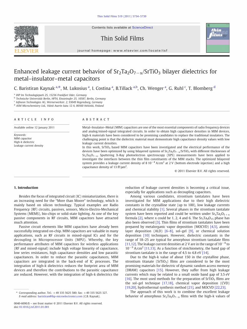
Cross sectional TEM images of the bilayered dielectrics with 3 nm,6 nm and 9 nm Sr2Ta2O7−x layers are shown in Fig. 3. The amorphouscharacter of the Sr2Ta2O7−x interlayer after the annealing step isvisible for each stack. Although the TiN/TaN bottom electrode stackhas a high roughness, even the 3 nm thick Sr2Ta2O7−x layer covers theelectrode surface uniformly due to the advantage of AVD technique. Inaddition, there is not any visible interfacial layer between Sr2Ta2O7−x
and TaN layer.Electricalmeasurementswere performed on the TaN/Sr2Ta2O7−x/
SrTiO3/Au MIM capacitors. Capacitance variation, measured at100 kHz can be approximated by the polynomial law:
C Vð Þ = C0 αV2 + βV + 1� �
ð1Þ
where α and β are the quadratic and linear coefficients, respectively.C0 represents capacitance at zero bias voltage. The extracted C0 valuesas a function of thickness are shown in Fig. 4. The single layer SrTiO3
MIM capacitor provides a high capacitance density of 17 fF/μm2. Withincreasing thickness of the underneath Sr2Ta2O7−x, the capacitancedensity is reduced to 9 fF/μm2. The dielectric constant of the pure
20 30 40 50 60102
103
104
105
106
SrT
iO3 1
10
SrT
iO3 1
11
SrT
iO3 2
00
SrT
iO3 2
11
TiN
111
TaN
111
Si 2
00
Inte
nsity
(cp
s)
Two Theta (degree)
b)
a)
Fig. 2. XRD patterns of samples after annealing process: a) reference sample (Si/TiN/TaN/SrTiO3), b) 9 nm Sr2Ta2O7−x deposited sample (Si/TiN/TaN/Sr2Ta2O7−x/SrTiO3).
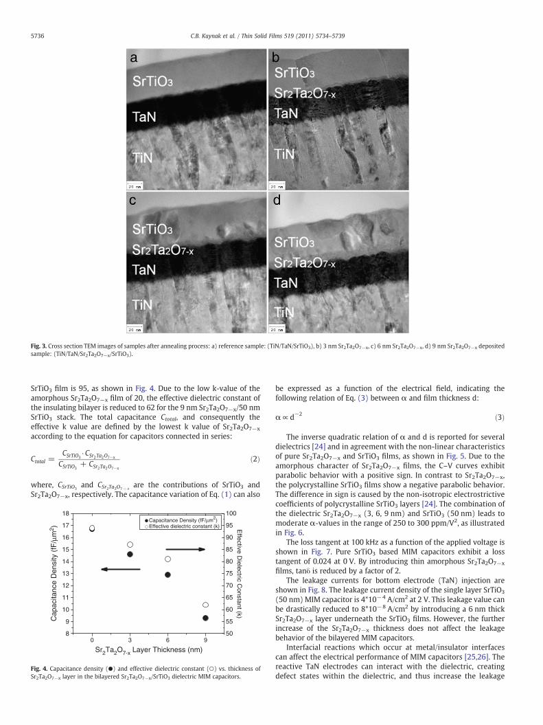
Fig. 3. Cross section TEM images of samples after annealing process: a) reference sample: (TiN/TaN/SrTiO3), b) 3 nm Sr2Ta2O7−x, c) 6 nm Sr2Ta2O7−x, d) 9 nm Sr2Ta2O7−x depositedsample: (TiN/TaN/Sr2Ta2O7−x/SrTiO3).
5736 C.B. Kaynak et al. / Thin Solid Films 519 (2011) 5734–5739
SrTiO3 film is 95, as shown in Fig. 4. Due to the low k-value of theamorphous Sr2Ta2O7−x film of 20, the effective dielectric constant ofthe insulating bilayer is reduced to 62 for the 9 nm Sr2Ta2O7−x/50 nmSrTiO3 stack. The total capacitance Ctotal, and consequently theeffective k value are defined by the lowest k value of Sr2Ta2O7−x
according to the equation for capacitors connected in series:
Ctotal =CSrTiO3 ⋅CSr2Ta2O7−x
CSrTiO3+ CSr2Ta2O7−x
ð2Þ
where, CSrTiO3and CSr2Ta2O7− x
are the contributions of SrTiO3 andSr2Ta2O7−x, respectively. The capacitance variation of Eq. (1) can also
0 3 6 98
9
10
11
12
13
14
15
16
17
18
Sr2Ta2O7-x Layer Thickness (nm)
Effective dielectric constant (k)
Cap
acita
nce
Den
sity
(fF
/μm
2 )
Capacitance Density (fF/μm2)
50
55
60
65
70
75
80
85
90
95
100
Effective D
ielectric Constant (k)
Fig. 4. Capacitance density (●) and effective dielectric constant (○) vs. thickness ofSr2Ta2O7−x layer in the bilayered Sr2Ta2O7−x/SrTiO3 dielectric MIM capacitors.
be expressed as a function of the electrical field, indicating thefollowing relation of Eq. (3) between α and film thickness d:
α∝ d−2 ð3Þ
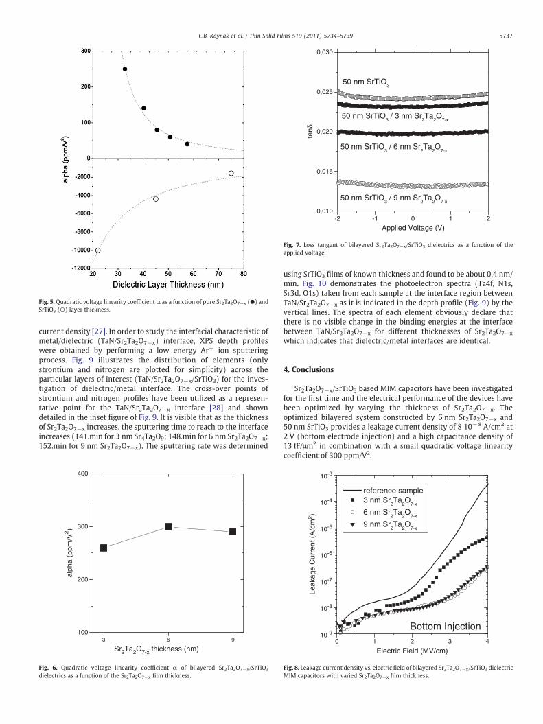
The inverse quadratic relation of α and d is reported for severaldielectrics [24] and in agreement with the non-linear characteristicsof pure Sr2Ta2O7−x and SrTiO3 films, as shown in Fig. 5. Due to theamorphous character of Sr2Ta2O7−x films, the C–V curves exhibitparabolic behavior with a positive sign. In contrast to Sr2Ta2O7−x,the polycrystalline SrTiO3 films show a negative parabolic behavior.The difference in sign is caused by the non-isotropic electrostrictivecoefficients of polycrystalline SrTiO3 layers [24]. The combination ofthe dielectric Sr2Ta2O7−x (3, 6, 9 nm) and SrTiO3 (50 nm) leads tomoderate α-values in the range of 250 to 300 ppm/V2, as illustratedin Fig. 6.
The loss tangent at 100 kHz as a function of the applied voltage isshown in Fig. 7. Pure SrTiO3 based MIM capacitors exhibit a losstangent of 0.024 at 0 V. By introducing thin amorphous Sr2Ta2O7−x
films, tanδ is reduced by a factor of 2.The leakage currents for bottom electrode (TaN) injection are
shown in Fig. 8. The leakage current density of the single layer SrTiO3
(50 nm)MIM capacitor is 4*10−4 A/cm2 at 2 V. This leakage value canbe drastically reduced to 8*10−8 A/cm2 by introducing a 6 nm thickSr2Ta2O7−x layer underneath the SrTiO3 films. However, the furtherincrease of the Sr2Ta2O7−x thickness does not affect the leakagebehavior of the bilayered MIM capacitors.
Interfacial reactions which occur at metal/insulator interfacescan affect the electrical performance of MIM capacitors [25,26]. Thereactive TaN electrodes can interact with the dielectric, creatingdefect states within the dielectric, and thus increase the leakage
-2 -1 0 1 20,010
0,015
0,020
0,025
0,030
50 nm SrTiO3 / 9 nm Sr
2Ta
2O
7-x
50 nm SrTiO3 / 6 nm Sr
2Ta
2O
7-x
50 nm SrTiO3 / 3 nm Sr
2Ta
2O
7-x
50 nm SrTiO3
tanδ
Applied Voltage (V)
Fig. 7. Loss tangent of bilayered Sr2Ta2O7−x/SrTiO3 dielectrics as a function of theapplied voltage.
Fig. 5. Quadratic voltage linearity coefficientα as a function of pure Sr2Ta2O7−x (●) andSrTiO3 (○) layer thickness.
5737C.B. Kaynak et al. / Thin Solid Films 519 (2011) 5734–5739
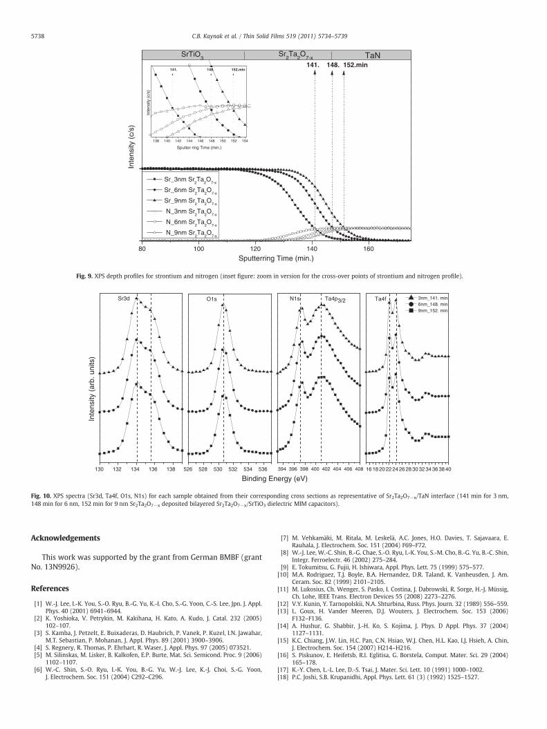
current density [27]. In order to study the interfacial characteristic ofmetal/dielectric (TaN/Sr2Ta2O7−x) interface, XPS depth profileswere obtained by performing a low energy Ar+ ion sputteringprocess. Fig. 9 illustrates the distribution of elements (onlystrontium and nitrogen are plotted for simplicity) across theparticular layers of interest (TaN/Sr2Ta2O7−x/SrTiO3) for the inves-tigation of dielectric/metal interface. The cross-over points ofstrontium and nitrogen profiles have been utilized as a represen-tative point for the TaN/Sr2Ta2O7−x interface [28] and showndetailed in the inset figure of Fig. 9. It is visible that as the thicknessof Sr2Ta2O7−x increases, the sputtering time to reach to the interfaceincreases (141.min for 3 nm Sr4Ta2O9; 148.min for 6 nm Sr2Ta2O7−x;152.min for 9 nm Sr2Ta2O7−x). The sputtering rate was determined
963100
200
300
400
alph
a (p
pm/V
2 )
Sr2Ta2O7-x thickness (nm)
Fig. 6. Quadratic voltage linearity coefficient α of bilayered Sr2Ta2O7−x/SrTiO3
dielectrics as a function of the Sr2Ta2O7−x film thickness.
using SrTiO3 films of known thickness and found to be about 0.4 nm/min. Fig. 10 demonstrates the photoelectron spectra (Ta4f, N1s,Sr3d, O1s) taken from each sample at the interface region betweenTaN/Sr2Ta2O7−x as it is indicated in the depth profile (Fig. 9) by thevertical lines. The spectra of each element obviously declare thatthere is no visible change in the binding energies at the interfacebetween TaN/Sr2Ta2O7−x for different thicknesses of Sr2Ta2O7−x
which indicates that dielectric/metal interfaces are identical.
4. Conclusions
Sr2Ta2O7−x/SrTiO3 based MIM capacitors have been investigatedfor the first time and the electrical performance of the devices havebeen optimized by varying the thickness of Sr2Ta2O7−x. Theoptimized bilayered system constructed by 6 nm Sr2Ta2O7−x and50 nm SrTiO3 provides a leakage current density of 8 10−8 A/cm2 at2 V (bottom electrode injection) and a high capacitance density of13 fF/μm2 in combination with a small quadratic voltage linearitycoefficient of 300 ppm/V2.
0 1 2 3 4
Bottom Injection
Leak
age
Cur
rent
(A
/cm
2 )
Electric Field (MV/cm)
reference sample 3 nm Sr
2Ta
2O
7-x
6 nm Sr2Ta
2O
7-x
9 nm Sr2Ta
2O
7-x
10-9
10-6
10-7
10-8
10-5
10-4
10-3
Fig. 8. Leakage current density vs. electric field of bilayered Sr2Ta2O7−x/SrTiO3 dielectricMIM capacitors with varied Sr2Ta2O7−x film thickness.
80 100 120 140 160
138 140 142 144 146 148 150 152 154
Inte
nsity
(c/
s)
Sputterring Time (min.)
Sr_3nm Sr2Ta
2O
7-x
Sr_6nm Sr2Ta
2O
7-x
Sr_9nm Sr2Ta
2O
7-x
N_3nm Sr2Ta
2O
7-x
N_6nm Sr2Ta
2O
7-x
N_9nm Sr2Ta
2O
7-x
141. 148. 152.min
SrTiO3
Sr2Ta
2O
7-x TaN
Inte
nsity
(c/
s)
Sputter ring Time (min.)
141. 148. 152.min
Fig. 9. XPS depth profiles for strontium and nitrogen (inset figure: zoom in version for the cross-over points of strontium and nitrogen profile).
16 18 20 22 24 26 28 30 32 34 36 38 40
3nm_141. min 6nm_148. min 9nm_152. min
Ta4f
130 132 134 136 138
Inte
nsity
(ar
b. u
nits
)
Sr3d
526 528 530 532 534 536
O1s
394 396 398 400 402 404 406 408
Binding Energy (eV)
N1s Ta4p3/2
Fig. 10. XPS spectra (Sr3d, Ta4f, O1s, N1s) for each sample obtained from their corresponding cross sections as representative of Sr2Ta2O7−x/TaN interface (141 min for 3 nm,148 min for 6 nm, 152 min for 9 nm Sr2Ta2O7−x deposited bilayered Sr2Ta2O7−x/SrTiO3 dielectric MIM capacitors).
5738 C.B. Kaynak et al. / Thin Solid Films 519 (2011) 5734–5739
Acknowledgements
This work was supported by the grant from German BMBF (grantNo. 13N9926).
References
[1] W.-J. Lee, I.-K. You, S.-O. Ryu, B.-G. Yu, K.-I. Cho, S.-G. Yoon, C.-S. Lee, Jpn. J. Appl.Phys. 40 (2001) 6941–6944.
[2] K. Yoshioka, V. Petrykin, M. Kakihana, H. Kato, A. Kudo, J. Catal. 232 (2005)102–107.
[3] S. Kamba, J. Petzelt, E. Buixaderas, D. Haubrich, P. Vanek, P. Kuzel, I.N. Jawahar,M.T. Sebastian, P. Mohanan, J. Appl. Phys. 89 (2001) 3900–3906.
[4] S. Regnery, R. Thomas, P. Ehrhart, R. Waser, J. Appl. Phys. 97 (2005) 073521.[5] M. Silinskas, M. Lisker, B. Kalkofen, E.P. Burte, Mat. Sci. Semicond. Proc. 9 (2006)
1102–1107.[6] W.-C. Shin, S.-O. Ryu, I.-K. You, B.-G. Yu, W.-J. Lee, K.-J. Choi, S.-G. Yoon,
J. Electrochem. Soc. 151 (2004) C292–C296.
[7] M. Vehkamäki, M. Ritala, M. Leskelä, A.C. Jones, H.O. Davies, T. Sajavaara, E.Rauhala, J. Electrochem. Soc. 151 (2004) F69–F72.
[8] W.-J. Lee, W.-C. Shin, B.-G. Chae, S.-O. Ryu, I.-K. You, S.-M. Cho, B.-G. Yu, B.-C. Shin,Integr. Ferroelectr. 46 (2002) 275–284.
[9] E. Tokumitsu, G. Fujii, H. Ishiwara, Appl. Phys. Lett. 75 (1999) 575–577.[10] M.A. Rodriguez, T.J. Boyle, B.A. Hernandez, D.R. Taland, K. Vanheusden, J. Am.
Ceram. Soc. 82 (1999) 2101–2105.[11] M. Lukosius, Ch. Wenger, S. Pasko, I. Costina, J. Dabrowski, R. Sorge, H.-J. Müssig,
Ch. Lohe, IEEE Trans. Electron Devices 55 (2008) 2273–2276.[12] V.Y. Kunin, Y. Tarnopolskii, N.A. Shturbina, Russ. Phys. Journ. 32 (1989) 556–559.[13] L. Goux, H. Vander Meeren, D.J. Wouters, J. Electrochem. Soc. 153 (2006)
F132–F136.[14] A. Hushur, G. Shabbir, J.-H. Ko, S. Kojima, J. Phys. D Appl. Phys. 37 (2004)
1127–1131.[15] K.C. Chiang, J.W. Lin, H.C. Pan, C.N. Hsiao, W.J. Chen, H.L. Kao, I.J. Hsieh, A. Chin,
J. Electrochem. Soc. 154 (2007) H214–H216.[16] S. Piskunov, E. Heifetsb, R.I. Eglitisa, G. Borstela, Comput. Mater. Sci. 29 (2004)
165–178.[17] K.-Y. Chen, L.-L. Lee, D.-S. Tsai, J. Mater. Sci. Lett. 10 (1991) 1000–1002.[18] P.C. Joshi, S.B. Krupanidhi, Appl. Phys. Lett. 61 (3) (1992) 1525–1527.

5739C.B. Kaynak et al. / Thin Solid Films 519 (2011) 5734–5739
[19] W.A. Feil, B.W. Wessels, L.M. Tonge, T.J. Marks, J. Appl. Phys. 67 (8) (1990)3858–3861.
[20] H. Holzschuh, H. Suhr, Adv. Mater. 4 (5) (1992) 357–359.[21] M.E. Pilleux, C.R. Grahman, V.M. Fuenzalida, J. Am. Ceram. Soc. 77 (1994)
1601–1604.[22] J.V. Mantese, A.L. Micheli, A.H. Hamdi, R.W. West, MRS Bull. (1989) 48–538
October.[23] G. Braunstein, G.R. Paz-Pujalt, Thin Solid Films 216 (1992) 1–3.[24] Ch. Wenger, G. Lupina, M. Lukosius, O. Seifarth, H.-J. Müssig, S. Pasko, Ch. Lohe,
J. Appl. Phys. 103 (2008) 104103.
[25] N. Gaillard, L. Pinzelli, M. Gros-Jean, A. Bsiesy, Appl. Phys. Lett. 89 (2006) 133506.[26] J.P. Chang, R.L. Opila, G.B. Alers, M.L. Stelgerwald, H.C. Lu, E. Garfunkel, T.
Gustafsson, Solid State Technol. 42 (1999) 43–48.[27] T. Remmel, R. Ramprasad, J. Walls, IEEE International, Dallas, Texas, March 30–
April 4, 2003, pp. 277–281.[28] G. Sjöblom, J. Westlinder, J. Olsson, IEEE Trans. Electron Devices 52 (2005)
2349–2352.