Electronic and magnetic properties of selected two ...
198
Electronic and magnetic properties of selected two–dimensional materials Dissertation zur Erlangung des Grades ” Doktor der Naturwissenschaften“ am Fachbereich Physik, Mathematik und Informatik der Johannes Gutenberg–Universit¨ at in Mainz von: Nils Richter geboren in T¨ ubingen Mainz, 2017
-
Upload
khangminh22 -
Category
Documents
-
view
2 -
download
0
Transcript of Electronic and magnetic properties of selected two ...
Electronic and magnetic properties ofselected two–dimensional materials
Dissertation
zur Erlangung des Grades
”Doktor der Naturwissenschaften“
am Fachbereich Physik, Mathematik und Informatik
der Johannes Gutenberg–Universitat
in Mainz
von:
Nils Richter
geboren in Tubingen
Mainz, 2017
ii
Nils Richter
Electronic and magnetic properties of selected two–dimensional materials
Datum der mundlichen Prufung: 20.02.2018
Johannes Gutenberg–Universitat Mainz
AG Klaui
Institut fur Physik
Staudingerweg 7
55128, Mainz
Eidesstattliche Erklarung
Hiermit erklare ich an Eides statt, dass ich meine Dissertation selbstandig und ohne
fremde Hilfe verfasst und keine anderen als die von mir angegebenen Quellen und Hilfs-
mittel zur Erstellung meiner Dissertation verwendet habe. Die Arbeit ist in vorliegender
oder ahnlicher Form bei keiner anderen Prufungsbehorde zur Erlangung eines Doktor-
grades eingereicht worden.
Mainz, den
Nils Richter
iii

This page was intentionally left blank.
Abstract
Electronic devices, such as field–effect transistors (FETs), based on low–dimensional
materials attract an immense interest as a potential inexpensive, flexible and trans-
parent next generation of electronics. There have been considerable improvements in
the accessibility of various low–dimensional materials and even the first ferromagnetic
monolayers have been experimentally realized. Nevertheless, many open questions re-
main concerning basic physical properties of such materials. This work focusses on the
electronic and magnetic properties of three carefully selected and especially interesting
low–dimensional materials: Bottom–up chemically synthesized graphene nanoribbons
(GNRs), nitrogen–doped graphene films and ferromagnetic chromium trihalides.
First, we investigate charge transport in bottom–up synthesized GNRs with various edge
morphologies and ribbon widths. Although prototypes of FET devices based on such
GNRs have recently been demonstrated, fundamental questions as for example on the
dominant charge transport mechanism, or on the structure– and width–dependence of
charge transport signatures in GNR devices, remain unanswered and need to be ad-
dressed experimentally. Therefore, we present the development of a reliable fabrication
of GNR network FETs and their measurement. In devices with gold electrodes at mi-
cron and submicron channel lengths, we study length–dependent charge transport as a
function of gate voltage and at a wide range of temperatures. First, we show that the
contact resistance is low and behaves Ohmic–like. The channel current follows power
laws for both temperature and drain voltage, which is explained by nuclear tunneling–
mediated hopping as the dominant charge transport mechanism. In addition, we observe
a large positive magnetoresistance of up to 14% at magnetic fields of 8 T at low temper-
atures. We find this magnetoresistance only in GNRs which have a width of five carbon
dimers across the ribbon and which are expected to exhibit a particularly low band gap.
With our results we provide a better understanding of the nature of charge transport
and the engineering of contacts, which both is evidently crucial to bolster any further
development of GNR–based devices.
v
Besides geometrical confinement in GNRs, we explore heteroatomic nitrogen doping as
a second route of tailoring charge transport properties of graphene. Here, extended
two–dimensional graphene films with substitutional nitrogen dopants are studied and
compared to pristine graphene fabricated under identical conditions. By combining
structural and electrical characterization methods, we elucidate the role of structural
disorder and electron localization for the electronic properties of this material induced
by the nitrogen dopants. We quantify the transition from weak to strong localization
with doping level based on the change of the length scales for phase coherent transport.
This transition is accompanied by a conspicuous sign change from positive ordinary
Kohler magnetoresistance in undoped graphene to large negative magnetoresistance in
doped graphene.
In addition to charge carrier properties, also spin properties depend heavily on the
dimensionality, where an important ingredient for stable magnetic order in lower dimen-
sions is magnetic anisotropy. Therefore, we investigate chromium trihalides, which are
layered and exfoliable semiconductors and exhibit unusual magnetic properties. In par-
ticular, we focus on the understanding of magnetocrystalline anisotropy by quantifying
the anisotropy constant of chromium iodide (CrI3), where we find a strong change from
5 K towards the Curie temperature. We draw a direct comparison to chromium bromide
(CrBr3), which serves as a reference, and where we find results consistent with literature.
In particular, we show that the anisotropy change in the iodide compound is more than
three times larger than in the bromide. We analyze this temperature dependence using
a classical model for the behavior of spins and spin clusters showing that the anisotropy
constant scales with the magnetization at any given temperature below the Curie tem-
perature. Hence, the temperature dependence can be explained by a dominant uniaxial
anisotropy where this scaling results from local spin clusters having thermally induced
magnetization directions that deviate from the overall magnetization.
Zusammenfassung
Elektronische Bauteile auf Basis niedrigdimensionaler Materialien, wie zum Beispiel
Feldeffekttransistoren (FETs), ziehen eine enorme Aufmerksamkeit auf sich. Sie haben
das Potential, die nachste Generation an kosteneffizienter, flexibler und transparenter
Elektronik zu bilden. Es hat bereits eine bemerkenswerte Entwicklung in der Verfugbarkeit
verschiedener niedrigdimensionaler Materialien gegeben, sodass sogar die ersten ferro-
magnetischen Monolagen experimentell untersucht werden konnten. Nichtsdestotrotz
sind viele grundlegenden physikalischen Eigenschaften nicht erforscht. Die vorliegende
Arbeit beschaftigt sich mit den elektronischen und magnetischen Eigenschaften dreier
sorgfaltig ausgewahlter niedrigdimensionaler Materialien: Chemisch bottom–up syn-
thetisierte Graphennanobander (GNRs), stickstoffdotierte Graphenfilme und ferromag-
netische Chromtrihalogenide.
Zuerst untersuchen wir Ladungstransport in bottom–up synthetisierten GNRs verschie-
dener Kantenmorphologien und Breiten. Obwohl erste FET–Prototypen basierend auf
GNRs demonstriert wurden, sind einige fundamentale Fragen immer noch unbeant-
wortet und verlangen nach einer experimentellen Klarung. Diese Fragen betreffen zum
Beispiel den Ladungstransportmechanismus oder die Struktur– und Breitenabhangigkeit
des Ladungstransports. Daher prasentieren wir die technische Entwicklung einer ver-
lasslichen Fabrikationsmethode von FETs basierend auf GNR–Netzwerken sowie die
Charakterisierung dieser Bauteile. Als Funktion von Gatterspannung und fur einen brei-
ten Temperaturbereich untersuchen wir den langenabhangigen Ladungstransport mit
Hilfe von FETs mit Goldelektroden und aktiven Kanalen im Bereich von einigen hun-
dert Nanometern bis hin zu einigen Mikrometern. Dabei zeigen wir zunachst, dass der
elektrische Kontaktwiderstand gering ist und sich ohmsch verhalt. Desweiteren bestim-
men Potenzgesetze das Verhalten des Kanalstroms in Abhangigkeit von Betriebsspan-
nung und Temperatur, was mit Hilfe von kerntunnelnassistiertem Ladungstragerhopping
als maßgeblichen Ladungstransportmechanismus erklart werden kann. Daruber hinaus
finden wir einen ausgepragten positiven Magnetowiderstand bis zu 14% bei Magnet-
feldern von 8 T und tiefen Temperaturen. Dieser Magnetowiderstand lasst sich dabei
allerdings ausschließlich in GNRs beobachten, die nur funf Kohlstoffdimerlangen breit
vii
sind und bei welchen eine besonders niedrige Bandlucke erwartet wird. Mit unseren
Ergebnissen tragen wir signifikant zu einem tieferen Verstandnis des Ladungstransport-
mechanismus bei und zeigen die Optimierung der elektrischen Kontakte auf. Beides ist
unerlasslich, um die Realisierung zukunftiger GNR–basierter Elektronik voranzutreiben.
Neben der geometrischen Einschrankung von Ladungstragern in GNRs, untersuchen wir
Fremdatomdotierung mit Stickstoff als zweite Strategie Ladungstransport in Graphen
maßzuschneidern. Dazu haben wir ausgedehnte zweidimensionale Graphenfilme mit
inkorporierter Stickstoffdotierung untersucht und vergleichen sie mit reinen Graphenfil-
men, welche unter identischen Bedingungen hergestellt wurden. Indem wir strukturelle
und elektronische Charakterisierungsmethoden miteinander verbinden, beleuchten wir
die Rolle von struktureller Ungeordnetheit sowie elektronischer Lokalisierung, welche
beide durch die Stickstoffdotierung induziert werden. Wir quantifizieren hierfur den, mit
zunehmendem Dotierungsniveau einhergehenden, Ubergang von schwacher zu starker
Lokalisierung auf Grundlage der Anderung der Langenskala von phasenkoharentem Trans-
port. Dieser Ubergang wird begleitet von einer bemerkenswerten Vorzeichenanderung
des Magnetowiderstands von gewohnlichem Kohlermagnetowiderstand in undotiertem
Graphen hin zu einem großen negativen Magnetowiderstand in dotiertem Graphen.
Nicht nur die Ladungstragereigenschaften hangen von der Dimensionalitat ab, sondern
auch die Eigenschaften von Spins. Hierbei ist magnetische Anisotropie ein wichtiger
Faktor, um magnetische Ordnung in niedrigen Dimensionen zu gewahrleisten. Da-
her untersuchen wir als dritten Themenbereich die magnetischen Eigenschaften von
Chromtrihalogeniden. Dies sind Halbleiterkristalle mit ungewohnlichen magnetischen
Eigenschaften und einer Schichtstruktur, wodurch sie sich zu Monolagen exfolieren
lassen. Wir untersuchen insbesondere die magnetokristalline Anisotropie, indem wir
die Anisotropiekonstante von Chromiodid (CrI3) als Funktion der Temperatur quan-
tifizieren. Wir beobachten dabei eine starke Anderung der magnetokristallinen Anisotro-
pie zwischen 5 K und der Curie–Temperatur. Diese vergleichen wir mit der von Chrom-
bromid (CrBr3), welches uns als Referenz dient, da es sich genauso verhalt, wie es fruhere,
der Literatur entnommene, Untersuchungen erwarten lassen. Insbesondere zeigen wir,
dass die Anisotropieanderung in der Iodidverbindung mehr als dreimal so stark ist wie im
Bromid. Die Temperaturabhangigkeit analysieren wir mit einem klassischen Model fur
Spins und Spinclustern und zeigen, dass bei gegebener Temperatur die Anisotropiekon-
stante mit der Magnetisierung skaliert. Folglich konnen wir unsere experimentellen
Beobachtungen mit einer dominant uniaxialen Anisotropie erklaren, bei welcher die
Skalierung das Resultat von lokalen Spinclustern ist, deren Magnetisierungsrichtung
durch thermische Aktivierung von der Ausrichtung der Gesamtmagnetisierung abweicht.
Dedicated to
my parents
Gewidmet
meinen Eltern
ix

Contents
Eidesstattliche Erklarung iii
Abstract v
Zusammenfassung vii
Contents xi
List of Figures xv
List of Tables xvii
Abbreviations xix
1 Introduction 1
2 Theoretical background 5
2.1 General effects of dimensional confinement in solid state systems . . . . . 5
2.1.1 Dimensional confinement of a particle . . . . . . . . . . . . . . . . 6
2.1.2 Density of states . . . . . . . . . . . . . . . . . . . . . . . . . . . . 7
2.2 Electronic properties of selected graphene allotropes . . . . . . . . . . . . 9
2.2.1 Single layer graphene . . . . . . . . . . . . . . . . . . . . . . . . . . 9
2.2.2 Turbostratic graphene multilayers . . . . . . . . . . . . . . . . . . 13
2.2.3 Geometrically confined graphene structures . . . . . . . . . . . . . 14
2.3 Charge transport by charge carrier hopping . . . . . . . . . . . . . . . . . 21
2.4 Basics of magnetism . . . . . . . . . . . . . . . . . . . . . . . . . . . . . . 23
2.4.1 Direct exchange . . . . . . . . . . . . . . . . . . . . . . . . . . . . . 23
2.4.2 Itinerant ferromagnetism . . . . . . . . . . . . . . . . . . . . . . . 24
2.4.3 Superexchange . . . . . . . . . . . . . . . . . . . . . . . . . . . . . 24
3 Experimental methods 27
3.1 Structural characterization by Raman spectroscopy . . . . . . . . . . . . . 27
3.2 Electrical measurements . . . . . . . . . . . . . . . . . . . . . . . . . . . . 30
3.2.1 Room temperature measurements . . . . . . . . . . . . . . . . . . 30
3.2.2 Low temperature measurements . . . . . . . . . . . . . . . . . . . 31
3.2.3 Current guarding . . . . . . . . . . . . . . . . . . . . . . . . . . . . 32
3.2.4 Van der Pauw technique . . . . . . . . . . . . . . . . . . . . . . . . 33
xi
Contents xii
3.3 SQUID magnetometry . . . . . . . . . . . . . . . . . . . . . . . . . . . . . 35
3.4 Electron beam lithography . . . . . . . . . . . . . . . . . . . . . . . . . . . 35
3.5 Sputtering . . . . . . . . . . . . . . . . . . . . . . . . . . . . . . . . . . . . 36
4 Development of charge transport test structures for graphene andgraphene nanoribbons 37
4.1 Synthesis of carbon materials . . . . . . . . . . . . . . . . . . . . . . . . . 38
4.1.1 Nitrogen–doped graphene . . . . . . . . . . . . . . . . . . . . . . . 38
4.1.2 Atomically precise graphene nanoribbons . . . . . . . . . . . . . . 39
4.1.3 Turbostratic graphene discs . . . . . . . . . . . . . . . . . . . . . . 41
4.2 Transfer technniques . . . . . . . . . . . . . . . . . . . . . . . . . . . . . . 42
4.2.1 Transfer of solution processable GNRs . . . . . . . . . . . . . . . . 42
4.2.2 Transfer of GNRs from surfaces . . . . . . . . . . . . . . . . . . . . 45
4.3 Device engineering for charge transport in bottom–up GNRs . . . . . . . 47
4.3.1 Short channel devices by lithography . . . . . . . . . . . . . . . . . 49
4.3.2 Short channel devices by electromigration in gold . . . . . . . . . . 53
4.3.3 Short channel devices by electromigration in turbostratic graphene 54
4.3.4 Long channel devices . . . . . . . . . . . . . . . . . . . . . . . . . . 59
4.4 Statistical analysis of the device yield . . . . . . . . . . . . . . . . . . . . 60
4.5 Conclusion and outlook . . . . . . . . . . . . . . . . . . . . . . . . . . . . 66
5 Charge transport in networks of bottom–up graphene nanoribbons 67
5.1 Experimental details . . . . . . . . . . . . . . . . . . . . . . . . . . . . . . 68
5.2 Electrical characterization of graphene nanoribbon–network field effecttransistors . . . . . . . . . . . . . . . . . . . . . . . . . . . . . . . . . . . . 70
5.2.1 Current–voltage characteristics . . . . . . . . . . . . . . . . . . . . 70
5.2.2 Doping effect of ambient gases . . . . . . . . . . . . . . . . . . . . 76
5.2.3 Determination of the electrical contact resistance at metal/graphenenanoribbon interfaces . . . . . . . . . . . . . . . . . . . . . . . . . 79
5.3 Charge transport mechanism in graphene nanoribbon networks . . . . . . 81
5.3.1 Universal scaling of charge transport . . . . . . . . . . . . . . . . . 81
5.3.2 Transport at low bias and low temperature . . . . . . . . . . . . . 85
5.4 Conclusion and outlook . . . . . . . . . . . . . . . . . . . . . . . . . . . . 87
6 Magnetoresistance and charge transport in graphene governed by ni-trogen dopants 89
6.1 Experimental details . . . . . . . . . . . . . . . . . . . . . . . . . . . . . . 90
6.2 Structural investigation using Raman spectroscopy . . . . . . . . . . . . . 92
6.3 Transport gap and charge carrier localization in doped graphene . . . . . 95
6.3.1 Charge carrier density and mobility probed by the Hall effect . . . 95
6.3.2 Variable range hopping conduction in nitrogen doped graphene . . 96
6.3.3 Positive and negative magnetoresistive effects . . . . . . . . . . . . 98
6.4 Conclusion and outlook . . . . . . . . . . . . . . . . . . . . . . . . . . . . 103
7 Magnetic properties of chromium trihalides 105
7.1 Magnetic properties of CrX3 . . . . . . . . . . . . . . . . . . . . . . . . . . 106
7.2 Experimental details . . . . . . . . . . . . . . . . . . . . . . . . . . . . . . 106
7.3 Temperature dependence of the magnetization . . . . . . . . . . . . . . . 108
Contents xiii
7.4 Magnetic hysteresis loops . . . . . . . . . . . . . . . . . . . . . . . . . . . 110
7.5 Magnetic anisotropy in CrI3 and CrBr3 . . . . . . . . . . . . . . . . . . . 112
7.6 Conclusions and outlook . . . . . . . . . . . . . . . . . . . . . . . . . . . . 114
8 Conclusion and outlook 117
A Additional material for Chapter 4 121
A.1 Raman mapping of graphene nanoribbon films on silicon dioxide . . . . . 122
B Additional material for Chapter 5 123
B.1 Raman spectra of various graphene nanoribbons . . . . . . . . . . . . . . 124
B.2 Current–voltage characteristics of networks of various GNR species . . . . 125
B.3 Gate–leakage and bias symmetry in GNR FET devices . . . . . . . . . . . 127
B.4 Determination of the field–effect mobility in GNR network FETs . . . . . 128
B.5 Charge transport statistics of GNR devices . . . . . . . . . . . . . . . . . 129
B.6 Estimation of the charge carrier density . . . . . . . . . . . . . . . . . . . 131
B.7 Doping and current annealing of GNR devices . . . . . . . . . . . . . . . . 133
B.8 Gate voltage–dependence of the contact resistance . . . . . . . . . . . . . 135
B.9 Conductance maps . . . . . . . . . . . . . . . . . . . . . . . . . . . . . . . 136
B.10 Temperature dependence of magnetotransport . . . . . . . . . . . . . . . . 137
C Additional material for Chapter 7 139
C.1 Additional experimental details . . . . . . . . . . . . . . . . . . . . . . . . 140
C.2 Hysteresis loops of chromium trihalides . . . . . . . . . . . . . . . . . . . 141
C.3 Degradation of chromium bromide in air . . . . . . . . . . . . . . . . . . . 142
Bibliography 143
Acknowledgements 175
Publications List 177

List of Figures
2.1 Graphene lattice in real and reciprocal space . . . . . . . . . . . . . . . . 10
2.2 Graphene band structure . . . . . . . . . . . . . . . . . . . . . . . . . . . 12
2.3 Graphene stacks . . . . . . . . . . . . . . . . . . . . . . . . . . . . . . . . 14
2.4 Armchair GNR and GNR nanowiggle . . . . . . . . . . . . . . . . . . . . . 16
2.5 aGNR bandstructure . . . . . . . . . . . . . . . . . . . . . . . . . . . . . . 18
2.6 GNRNW bandstructure . . . . . . . . . . . . . . . . . . . . . . . . . . . . 19
3.1 Stokes and Anti–Stokes Processes . . . . . . . . . . . . . . . . . . . . . . . 28
3.2 Raman spectrum of graphene . . . . . . . . . . . . . . . . . . . . . . . . . 29
3.3 Sample holder for cryostat . . . . . . . . . . . . . . . . . . . . . . . . . . . 31
3.4 Electrical measurements with driven guard . . . . . . . . . . . . . . . . . 32
3.5 Van der Pauw measurement schemes . . . . . . . . . . . . . . . . . . . . . 34
4.1 Collection of bottom–up synthesized GNR structures . . . . . . . . . . . . 40
4.2 GNR films on HOPG and SiO2 . . . . . . . . . . . . . . . . . . . . . . . . 43
4.3 Optimized GNR film on SiO2 . . . . . . . . . . . . . . . . . . . . . . . . . 44
4.4 Transfer of CVD–grown GNR films to a target substrate . . . . . . . . . . 46
4.5 Schematic depiction of a GNR FET . . . . . . . . . . . . . . . . . . . . . 48
4.6 Flow chart of the production of lithographically defined short channeldevices . . . . . . . . . . . . . . . . . . . . . . . . . . . . . . . . . . . . . . 50
4.7 Metallic nanojunction defined by EBL . . . . . . . . . . . . . . . . . . . . 51
4.8 Metallic nanojunction defined by EM . . . . . . . . . . . . . . . . . . . . . 54
4.9 Flow chart of the production of TG–based electromigrated short channeldevices . . . . . . . . . . . . . . . . . . . . . . . . . . . . . . . . . . . . . . 55
4.10 SEM image of a two–terminal EM device with TG disc . . . . . . . . . . . 57
4.11 EM of TG discs . . . . . . . . . . . . . . . . . . . . . . . . . . . . . . . . . 58
4.12 Flow chart of the production of lithographically defined long channel devices 59
4.13 Large channel device defined by EBL . . . . . . . . . . . . . . . . . . . . . 61
4.14 Success rates of GNR device production approaches . . . . . . . . . . . . 64
5.1 Raman spectrum of aGNR 9 and aGNR 5 . . . . . . . . . . . . . . . . . . 69
5.2 Current–Voltage–characteristics of aGNR 5 and aGNR 9 networks . . . . 71
5.3 Impact of unintentional doping on the electrical properties of GNR net-work FETs . . . . . . . . . . . . . . . . . . . . . . . . . . . . . . . . . . . 77
5.4 Contact resistance of metal/GNR interfaces . . . . . . . . . . . . . . . . . 80
5.5 Temperature dependent charge transport in GNR networks . . . . . . . . 82
5.6 Scaling of the current–voltage characteristics of GNR network FETs . . . 83
5.7 Transport at low temperatures and low bias voltages . . . . . . . . . . . . 86
xv
List of Figures xvi
6.1 Raman spectra of undoped and doped graphene . . . . . . . . . . . . . . . 93
6.2 Sheet resistance vs. temperature . . . . . . . . . . . . . . . . . . . . . . . 97
6.3 Sheet resistance vs. magnetic field . . . . . . . . . . . . . . . . . . . . . . 99
6.4 Weak localization in undoped graphene and doped graphene . . . . . . . . 102
7.1 Image collection of CrX3 crystals (X=I, Br, Cl) . . . . . . . . . . . . . . . 107
7.2 Magnetization vs. temperature . . . . . . . . . . . . . . . . . . . . . . . . 109
7.3 Hysteresis loops . . . . . . . . . . . . . . . . . . . . . . . . . . . . . . . . . 111
7.4 Magnetocrystalline anisotropy . . . . . . . . . . . . . . . . . . . . . . . . . 113
7.5 Scaling of Ku . . . . . . . . . . . . . . . . . . . . . . . . . . . . . . . . . . 114
7.6 Exfoliation of CrBr3 . . . . . . . . . . . . . . . . . . . . . . . . . . . . . . 115
A.1 Thin films of CVD–grown GNRs . . . . . . . . . . . . . . . . . . . . . . . 122
B.1 Raman spectrum of aGNR 7, GNRNW (9,6),(2,15), GNRNW N–N (9,6),(2,15)and GNRNW N–S (9,6),(2,15) . . . . . . . . . . . . . . . . . . . . . . . . 124
B.2 Current–Voltage–characteristics of aGNR 7 and GNRNW (9,6),(2,15)networks . . . . . . . . . . . . . . . . . . . . . . . . . . . . . . . . . . . . . 125
B.3 Current–Voltage–characteristics of GNRNW N–N (9,6),(2,15) and GN-RNW N–S (9,6),(2,15) networks . . . . . . . . . . . . . . . . . . . . . . . . 126
B.4 Gate leakage and bias symmetry in aGNR 5 and aGNR 9 devices . . . . . 127
B.5 Temperature dependence of charge carrier density in the aGNR 5 and theaGNR 9 devices . . . . . . . . . . . . . . . . . . . . . . . . . . . . . . . . . 131
B.6 Box plot of device resistances before and after air exposure . . . . . . . . 133
B.7 Impact of current annealing on current modulation by electrostatic gating 134
B.8 Contact resistance as function of gate voltage . . . . . . . . . . . . . . . . 135
B.9 Conductance maps at low temperature for aGNR 5 and aGNR 9 . . . . . 136
C.1 Full hysteresis loops of CrX3 . . . . . . . . . . . . . . . . . . . . . . . . . 141
C.2 Degradation of CrBr3 . . . . . . . . . . . . . . . . . . . . . . . . . . . . . 142
List of Tables
4.1 Overview of GNR long channel devices . . . . . . . . . . . . . . . . . . . . 65
5.1 Statistics for charge tranport parameters of GNR networks . . . . . . . . 74
5.2 Concact resistances in aGNR 5 devices . . . . . . . . . . . . . . . . . . . . 79
6.1 Raman peak positions of undoped graphene and doped Graphene . . . . . 93
6.2 Overview of charge transport parameters in undoped graphene and dopedgraphene . . . . . . . . . . . . . . . . . . . . . . . . . . . . . . . . . . . . . 102
7.1 Overview of magnetic properties of CrX3 . . . . . . . . . . . . . . . . . . 107
8.1 Overview of electronic properties of various graphene materials . . . . . . 118
B.1 Charge transport statistics aGNR 9 Chip 2 . . . . . . . . . . . . . . . . . 129
B.2 Charge transport statistics aGNR 5 Chip 1 . . . . . . . . . . . . . . . . . 129
B.3 Charge transport statistics aGNR 5 Chip 2 . . . . . . . . . . . . . . . . . 129
B.4 Charge transport statistics aGNR 5 Chip 4 . . . . . . . . . . . . . . . . . 130
B.5 Charge transport statistics aGNR 5 Chip 5 . . . . . . . . . . . . . . . . . 130
B.6 Charge transport statistics aGNR 5 Chip 6 . . . . . . . . . . . . . . . . . 130
B.7 Temperature dependence of magnetotransport in aGNR 5 . . . . . . . . . 137
C.1 CrX3 crystal masses . . . . . . . . . . . . . . . . . . . . . . . . . . . . . . 140
xvii

Abbreviations
1D one dimensional
2D two dimensional
2DEG two–dimensional electron gas
aGNR graphene nanoribbon with armchair edges
AFM atomic force microscopy
BLG bilayer graphene
chGNR graphene nanoribbon with chevron–type edges
CNT carbon nanotube
CVD chemical vapor deposition
DFT density functional theory
DOS density of states
EBL electron beam lithography
EL ethyl lactate
EM electromigration
FBZ first Brillouin zone
FET field–effect transistor
FLG few–layer graphene
FWHM full width at half maximum
GNR graphene nanoribbon
GNRNW GNR nanowiggle
HF hydrofluoric acid
HOPG highly oriented pyrolytic graphite
LBM layer breathing mode
LPE liquid phase exfoliation
MAA methacrylic acid
xix
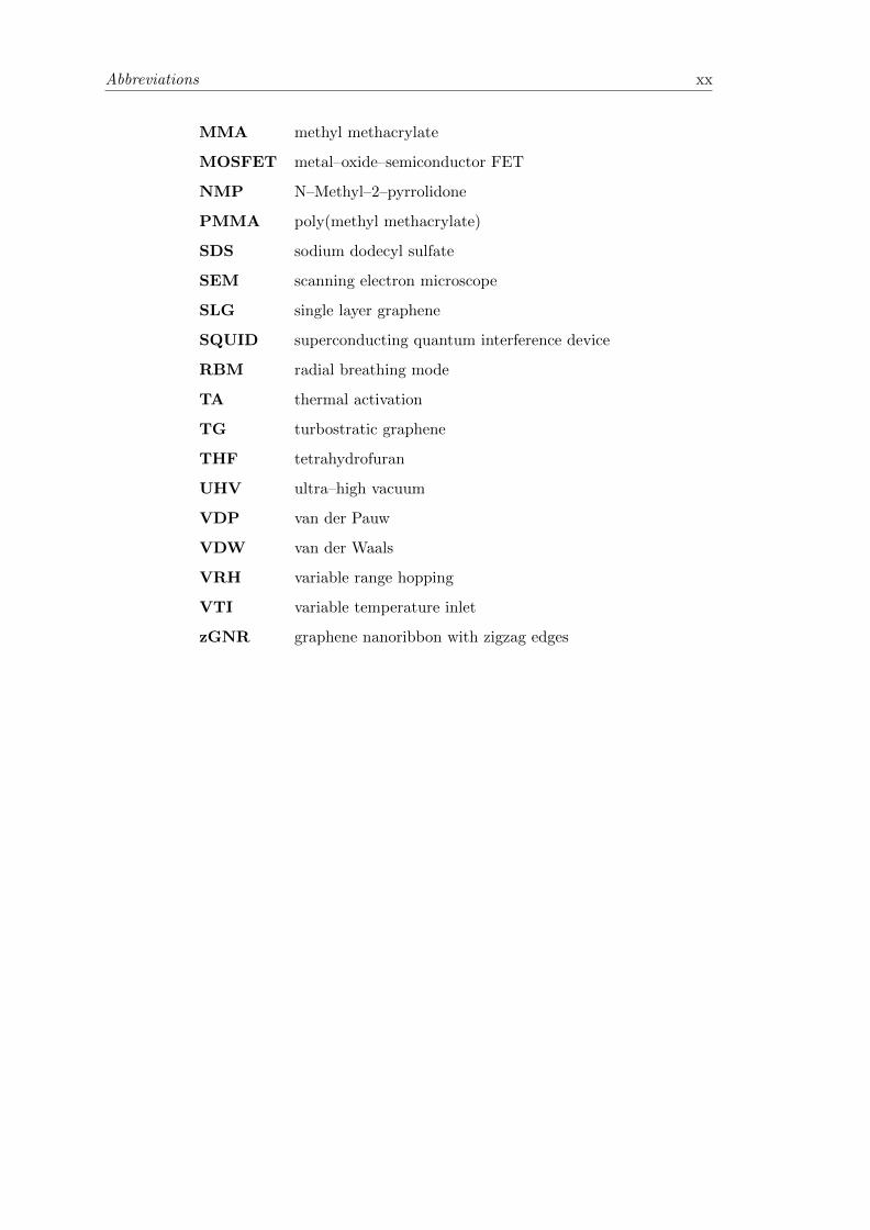
Abbreviations xx
MMA methyl methacrylate
MOSFET metal–oxide–semiconductor FET
NMP N–Methyl–2–pyrrolidone
PMMA poly(methyl methacrylate)
SDS sodium dodecyl sulfate
SEM scanning electron microscope
SLG single layer graphene
SQUID superconducting quantum interference device
RBM radial breathing mode
TA thermal activation
TG turbostratic graphene
THF tetrahydrofuran
UHV ultra–high vacuum
VDP van der Pauw
VDW van der Waals
VRH variable range hopping
VTI variable temperature inlet
zGNR graphene nanoribbon with zigzag edges
Chapter 1
Introduction
In 2004, the pioneering experiments on graphene [1], a planar arrangement of carbon
atoms in a honeycomb lattice, marked the starting point for a new paradigm in solid
state physics. This paradigm of self–supported two–dimensional (2D) crystals has been
fully established soon afterwards, when it was realized that layered crystals other than
graphite, such as hexagonal boron nitride or transition metal dichalcogenides, can also
be subjected to the method of micromechanical cleavage yielding stable monolayers
[2]. Since the parental bulk crystals usually have weak interlayer bonds based on van
der Waals (VDW) interactions, they are also commonly labeled VDW materials. The
number of accessible monolayer materials is steadily increasing and while often they
are intriguing on their own (e.g. graphene, MoS2 [3] or black phosphorus [4]), a great
potential lies in further tailoring their electronic, magnetic and optical properties. In
this thesis, we investigate three carefully selected representatives of highly promising
VDW material classes, namely atomically perfect bottom–up graphene nanoribbons,
nitrogen–doped single layer graphene and chromium trihalides. The choice of these
particular materials is motivated by their exceptional electronic and magnetic features
which render them capable to realize such an aforementioned customization, paving the
way towards new and exciting physical phenoma in reduced dimensions.
Geometrical confinement allows one to severely modify the properties a solid state sys-
tem and therefore graphene nanoribbons (GNRs), which are confined graphene systems,
stand in the focus of this work. In GNRs, the electronic structure depends crucially
1
Chapter 1. Introduction 2
on the width and the details of the edge morphology, where the latter knows two pro-
totypical shapes, armchair and zigzag edges [5]. The development of charge transport
devices based on such structures is of particular interest for both scientific research and
industry, due to the special properties of GNRs. For example, a band gap arises which
is extremely sensitive to the ribbon width. Increasing the latter by only one row of
carbon atoms along an armchair GNR can result in a dramatic change of the band gap
size, where the band gaps of such two GNRs can exhibit differences in the order of
electronvolts [6]. Tuning this band gap opens new possibilities to approach the limits
of nano–scale electronics with custom–made characteristics. Secondly, zigzag GNRs ex-
hibit localized electronic states, which have been predicted to be magnetic [7], enabling
ultra–small spintronic devices with novel functionalities. Modern chemistry allows for
the bottom–up synthesis of these carbon nanostructures with precision on the atomic
level and with remarkable flexibility in terms of the two aforementiond parameters, width
and edge structure. In this work, we make use of this unique opportunity to synthesize
and process such well–defined systems and conduct a systematic experimental study of
charge transport in a variety of GNR types.
Secondly, another route to the modification of graphene’s electronic properties is het-
eroatomic doping. Heteroatomic dopants are either incorporated in the lattice replacing
carbon atoms [8], physisorbed to the graphene surface while leaving the lattice intact
[9, 10], or both approaches can be combined leading to new types of devices [11]. Fur-
thermore, heteroatomic doping even has the potential to open up a band gap [12–14].
Dopant concentrations of more than 15 % have already been reached experimentally
with nitrogen and boron [15–18]. However, while the band gap increased in the boron
doped graphene, the mobility decreased due to a higher amount of scattering effects [16].
This result indicates that the requirements for any device have to be carefully weighed
against each other [15]. Improvements regarding one of the material’s properties might
lead to an undesired change of another one. In order to elucidate such alterations,
we investigate in–depth how nitrogen (N) doping affects charge transport properties of
graphene, where nitrogen atoms are incorporated into the lattice during the synthesis by
chemical vapor deposition (CVD). Using both, electrical and structural characterization
(by Raman spectroscopy), we can relate changes of charge carrier properties to changes
in the structure of the material.
Chapter 1. Introduction 3
Finally, chromium trihalides, CrX3 with X being a halogen ion of fluorine (F), chlorine
(Cl), bromine (Br) or iodine (I), are a particular case of layered seminconductors with
unusual and exciting magnetic properties. Compared to unmagnetic materials, magnet-
ically ordered ones are largely underrepresented in the list of VDW materials [19] and
recently ferromagnetism in a single CrI3 layer has been experimentally demonstrated
[20]. The synthesis of CrX3 can be realized by CVD [21, 22] and they can be readily
exfoliated using the same scotch tape technique which initially yielded graphene mono-
layers [1]. While CrX3 compounds have been studied initially as bulk materials in the
1960s pioneered by Tsubokawa, Dillon and Hansen [23–26], the prospect of magnetic
single layers of these materials is a source of a renewed interest. The possibility of han-
dling single layers of various materials and combining them in arbitrary ways offers an
immense flexibility and an unprecedented opportunity to create artifical designer stacks.
In these stacks, exciting phenoma are emerging from the physics at the interfaces, espe-
cially when magnetic layers are integrated [27, 28]. However, magnetism of CrX3 is still
not well–understood and in order to serve as a basis for the understanding of magnetic
phenomena in reduced dimensions, remaining open questions need to be addressed [22].
The thesis is organized as follows:
Chapter 2 is an introduction to the physics of two–dimensional materials, especially
describing the theoretical background of graphene and graphene nanoribbons. Further-
more, the basics of magnetism are reiterated in order to build a foundation for the
understanding of magnetic phenomena in chromium trihalides.
Chapter 3 presents an overview of all experimental techniques that have been used
throughout this thesis to characterize GNRs, doped graphene and CrX3 compounds.
The details of the experimental setups are given in this chapter.
Chapter 4 shows the engineering process of charge transport test structures, especially
to probe charge transport in GNRs. Since atomically perfect GNRs have not been avail-
able for a long time, there is no standard procedure to contact them and the achievement
of a reliable device fabrication route is a major step forward in this field.
Chapter 5 is dedicated to the experiments of charge transport through GNR networks.
Various types of GNRs have been measured and we compare our experimental results
in this chapter, especially focussing on armchair GNRs with two different widths of five
Chapter 1. Introduction 4
and nine carbon atoms across the ribbon, respectively. Their electrical characterization
has been extended to variable temperatures and high magnetic fields.
Chapter 6 deals with nitrogen doped graphene. A characterization of the structural
integrity of CVD–grown N–doped graphene films is presented here, combined with
charge transport, again at variable temperatures and at high magnetic fields. Our mea-
surements demonstrate the relation between structure and functionality in this special
graphene allotrope.
Chapter 7 presents our experimental results on the magnetic properties of chromium
trihalides. Magnetometry on bulk single crystals enables us to understand the magne-
tocrystalline anisotropy in these compounds, which is the key to stable ferromagnetism
down to the monolayer regime.
Chapter 8 finally concludes this thesis by summarizing and highlighting the major
results of chapters 4 – 7. The chapter also includes an outlook of promising future
research.
The results presented in this dissertation have, in parts, already been published or
submitted to different journals. A list of publications is presented at the end of this
thesis. Furthermore, references are included in the text wherever appropriate.
Chapter 2
Theoretical background
In a low–dimensional system the motion or arrangement of particles and other entities,
such as magnetic moments, is constrained to a plane (2D) or to a chain (1D). Often new
and exciting physical effects emerge from such geometrical confinement. For example, in
graphene, a monolayer of carbon atoms in a hexagonal lattice, massless Dirac fermions
exhibiting unusual properties are a consquence of the two–dimensional structure [29]. In
this chapter, we provide a theoretical description of the effects of geometrical confinement
going from two–dimensional confinement in graphene to one–dimensional confinement in
graphene nanoribbons. Furthermore, we give a brief introduction to magnetic exchange
effects, relevant for the magnetic coupling in chromium trihalogenides, a class of layered
magnetic semiconductors.
2.1 General effects of dimensional confinement in solid
state systems
Numerous physical problems are best described in three (spatial) dimensions. However,
certain properties drastically change when the dimensionality of a system is confined. In
solid state physics, widely discussed examples are planar spin arrangements (Ising model)
[30] or low–dimensional semiconductor heterostructures [31]. Especially the latter have
had a broad impact on semiconductor physics and technology as, for instance, semicon-
ductor lasers [32] or ultrafast transistors [33] were realized using semiconductor–based
quantum wells and two–dimensional electron gases (2DEGs). Founded on fundamental
5
Chapter 2. Theoretical background 6
quantum mechanics, a whole formalism can be developed in order to describe properties
of low–dimensional semiconductor physics (see e.g. Ref. [31] for further reading) and
here we recapitulate only a selection of important concepts. First, we have a closer
look at the general idea of confinement and secondly, we discuss the electronic density
of states in one, two and three dimensions, which is a particularly useful quantity to
understand the electronic and optical properties of a system.
2.1.1 Dimensional confinement of a particle
While a completely unbound electron can propagate in all three spatial dimensions, a
narrow potential well can be used to restrict this motion in one dimension to discrete
energy levels. If the separation of such energy levels is large, the only energy level
accessible for such an electron at low energy is the ground state and no motion will
be possible in this dimension. This way electrons can be confined into two dimensions
(2DEGs) or even into one dimension (quantum wires). To understand the confinement
in more detail, we follow the considerations in Ref. [31] and start with the three–
dimensional time–independent Schrodinger equation for one particle with mass m
[− ~2
2m∇2 + V (R)
]Ψ(R) = EΨ(R) , (2.1)
where R is the three–dimensional position vector, Ψ is the wave function of the particle,
V denotes the potential energy, ∇ is the tree–dimensional nabla operator, ~ is the
reduced Planck constant and E is the energy. We now consider a potential which confines
the motion in only one dimension, i.e. in z direction. Hence, we can write V (R) = V (z)
and the particle is still free to move along x and y direction. This motivates to write
the wave function as a product of plane waves for x and y and an unknown function,
u(z), for z:
Ψ(x, y, z) = exp (i kx x) exp (i ky y)u(z) . (2.2)
After substituting this into the Schrodinger equation, we can let the partial derivatives
act on the exponential functions. The exponential functions then cancel from both sides
and only the dependence on z remains. After sorting constant terms to the right–hand
Chapter 2. Theoretical background 7
side, we obtain
[− ~2
2m
d2
dz2+ V (z)
]u(z) =
[E − ~2 k2
x
2m−
~2 k2y
2m
]u(z) = ε u(z) . (2.3)
In order to solve Eq. 2.3, we need to know the exact form of the potential energy. In
either case, the energy is quantized along the z direction and the eigenenergies of the
system are of the form
En(kx, ky) = εn +~2 k2
x
2m+
~2 k2y
2m, (2.4)
where the quantum numbers kx, ky and n label the states in each dimension. The
infinetly deep square quantum well is the simplest example of such a confining potential
and although it cannot be experimentally realized it is particularly useful to approximate
finite quantum wells (e.g. in a GaAs–AlGaAs system) because of its simplicity [31].
There is a straight–forward way to extend the confinement to other dimensions. If we
chose a potential of the form V (R) = V (x, y), the result is a quantum wire, where
the particle remains free to move only along z. As we will see by the example of one–
dimensional graphene nanoribbons in Sec. 2.2.3, such confinement has a significant
impact on the electronic properties as large band gaps can be formed. If the potential
confines the particle in all three dimensions, there is no free motion in any dimension and
the result is called a quantum dot. Quantum dots exhibit then energy levels analoguous
to atoms and therefore they are often called artifical atoms.
2.1.2 Density of states
The density of states (DOS) for electrons, N(E) δE, is one of the most important quan-
tities to understand and describe a quantum system and its distribution of energies in
an intervall [E;E+ δE]. The DOS is useful in countless examples, as in magnetism (e.g.
for defining the Stoner criterion, see Sec. 2.4.2) or in quantum-well lasers [31]. A general
definition of the total DOS of a system with eigenenergies εn is
N(E) =∑n
δ(E − εn) , (2.5)
where δ(E) denotes the Dirac δ–distribution. In order to determine the total number of
states between E1 and E2, Eq. 2.5 has to be integrated over this interval and then the
sum has to be evaluated. We can now consider free electrons in one dimension. Their
Chapter 2. Theoretical background 8
states can be labled by their wave number k, such that Eq. 2.5 becomes
N(E) = 2
∞∑k=−∞
δ[E − ε0(k)] , (2.6)
where the factor 2 accounts for spin. The simplest way to treat the problem of free
electrons in one dimension is to consider them being trapped in a finite box of length
L and perfom the limit L → ∞ at the end of the calculation. Following this route,
one can readily show that the eigenstates of this system are regularly spaced in k–space
with a separation of 2π/L [31]. Hence, for large systems, we can use a continuum
approximation and replace the sum in 2.6 by an integral
N(E) =L
π
∫ ∞−∞
δ[E − ε0(k)] dk . (2.7)
This integral can be easily solved by substitution using the relation ε0(k) = ~2 k2/(2m)
and we arrive at
N1D(E) =2L
π ~
∫ ∞0
√m
2 zδ[E − z] dz =
L
π ~
√2m
E. (2.8)
In Eq. 2.8, we see that the DOS diverges as E−1/2 in the limit E → 0 (Van Hove
singularities [34]), which is a characteristic feature of one dimension and can be found for
carbon nanotubes (CNTs) and graphene nanoribbons (GNRs). In the case of parabolic
band dispersion, the density of states is constant in two dimensions and ∝√E in three
dimensions. For linear bands however, the DOS is ∝ |E| in two dimensions (e.g. in
graphene) and ∝ E2 in three dimensions.
Chapter 2. Theoretical background 9
2.2 Electronic properties of selected graphene allotropes
Carbon is an abundant element on earth with a large variety of allotropes [35]. In 2004,
K. Novoselov et al. achieved a milestone in carbon research as the electric field effect
in graphene was demonstrated [1]. These experiments were the starting point for a new
and fruitful field of science. Materials beyond graphene, as for example geometrically
confined graphene or graphene multilayers, exhibit further exciting properties. However,
as the electronic properties of an ideal sheet of graphene are the basis to understand
such more complicated systems, we start with this as an introduction.
2.2.1 Single layer graphene
A common way to derive the electronic structure of graphene [29, 36] is to employ the
tight–binding method [37]. In this section, we discuss the key aspects of this approach
and its results as a basis for the understanding of confined structures. The building
blocks of the graphene lattice are carbon atoms which have four valence electrons partic-
ipating in the formation of chemical bonds. In graphene, the atomic s orbital hybridizes
with two p orbitals (sp2 hybridization), leading to a planar arrangement of all carbon
atoms. In the plane, σ bonds form an angle of 120 and π orbitals arrange perpendicular
to the plane. Thus, we obtain a two-dimensional hexagonal lattice. Every carbon atom
has three nearest neighbors at a distance of a = 1.42 A. We choose a certain carte-
sian coordinate system1 and make use of the hexagonal symmetry to find three vectors,
connecting nearest neighbors:
δ1 =a
2
(1,√
3)T
, δ2 =a
2
(1,−√
3)T
δ3 = −a (1, 0)T . (2.9)
However, not all sites are equivalent and one can find a decomposition of the hexagonal
lattice into two triangular Bravais sublattices A and B.
1The choice of the origin and the axes of the coordinate system is arbitrary. However, once chosen ithas to be consistently used in consecutive analysis [38].
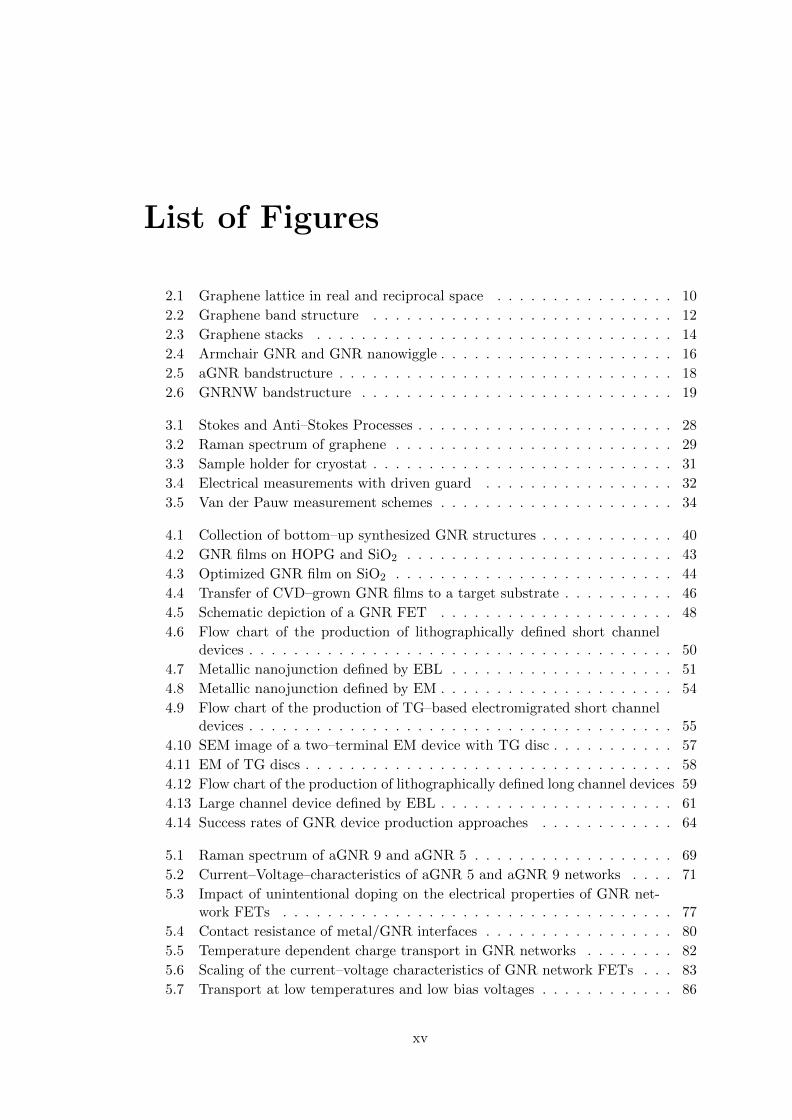
Chapter 2. Theoretical background 10
a2
a1 δ1
δ2
δ3
zigz
aged
ge
armchair edgex
y
kx
ky
Γ
K ′
K
b1
b2
(a) Real space (b) First Brillouin zone
Figure 2.1: Graphene honeycomb lattice and its first Brillouin zone. (a) The hexago-nal lattice in real space which consists of two triangular sublattices A (open dots) andB (solid dots). The vectors a1 and a2 are the primitive vectors of sublattice A and δi,i = 1, 2, 3 are the nearest neighbor vectors. Two axes of high symmetry can be foundin the hexagonal lattice: armchair (blue dotted line) and zigzag (red dashed line). (b)Corresponding Brillouin zone. The vectors b1 and b2 span the reciprocal lattice. Thecenter (Γ point) and the two inequivalent corners (K and K ′) of the Brillouin zone arelabeled.
In the same coordinate system, the primitive vectors, e.g. of sublattice A, are given by
a1 =a
2
(3,√
3)T
, a2 =a
2
(3,−√
3)T
, (2.10)
and their counterparts in reciprocal space are
b1 =2π
3 a
(1,√
3)T
, b2 =2π
3 a
(1,−√
3)T
, (2.11)
which fulfill the condition ai · bj = 2π δij , where i = 1, 2 and δij is the Kronecker delta.
Figure 2.1 schematically shows the graphene lattice in real space as well as the first
Brillouin zone (FBZ) which is the first Wigner–Seitz cell [39] of the triangular lattice
in reciprocal space. Neighboring corners in the FBZ are inequivalent as they are not
connected by reciprocal lattice vectors and they are conventionally labeled K and K ′.
These crystallographic points usually coincide with so–called “Dirac” points in graphene
(see below) [40]. The lattice symmetries will now help us to understand the electronic
structre. As we are interested in the transport properties of graphene and its related
materials, we consider only the π electrons because they are delocalized and not localized
in covalent bondings. Within the tight–binding approach, we assume that an electron
can hop from lattice site to lattice site, with amplitudes t when hopping between nearest
Chapter 2. Theoretical background 11
neighbors and t′ when hopping between next–nearest neighbors2. In the language of
second quantization this situation can be modeled by introducing annihilation (creation)
operators ai,σ, bj,σ (a†i,σ, b†j,σ) which annihilate (create) an electron with spin σ (σ = ↑, ↓)
at lattice sites Ri and Rj of the sublattices A and B, respectively:
H = −t∑〈i,j〉,σ
(a†σ,i bσ,j + H.c.
)− t′
∑〈〈i,j〉〉,σ
(a†σ,i aσ,j + b†σ,i bσ,j + H.c.
). (2.12)
The sum in the first term runs over all nearest-neighbor sites 〈i, j〉, while the sum in
the second term considers the next–nearest neighbor sites 〈〈i, j〉〉. The symbol H.c.
denotes the Hermitian conjugate of the preceding term. Without loss of generality, we
restrict the following calculation to nearest–neighbor hopping and perform a Fourier
transformation of the annihiliation (creation) operators such that
ai,σ =1
N
∑k
eikRi ak,σ, bj,σ =1
N
∑k
eikRj bk,σ . (2.13)
Here, we choose the same phase factor for the two sublattices [38] and N is the number of
unit cells. Reintroducing these operators into the Hamiltonian (Eq. 2.12) and computing
the sum over the lattice sites, we find the Hamiltonian in momentum space
H = −t∑σ,k
(γk a
†σ,k bσ,k′ + γ∗k b
†σ,k aσ,k′
), (2.14)
where we have used γk =∑3
i=1 eik·δi . In a final step of algebraic transformation, we
rewrite Eq. 2.14 in a matrix and spinor notation,
H =∑
Ψ†kσ ·A ·Ψkσ , (2.15)
with A =
0 −t γk−t γ∗k 0
and Ψσ,k =
aσ,kbσ,k
. In order to derive the energy spectrum
we now calculate the eigenvalues εk of the matrix A. The result is given by
εk = ±t · |γk| . (2.16)
2The value t is approximately 2.8 eV [29], while t′ is not well known. From ab initio calculations arange of 0.02 t ≤ t′ ≤ 0.2 t is predicted [41]. A tight-binding fit to cyclotron resonance experiments findst′ ≈ 0.1 eV [42].
Chapter 2. Theoretical background 12
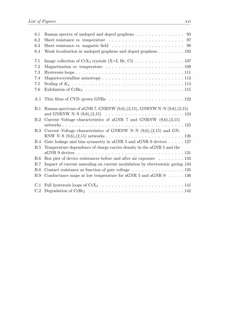
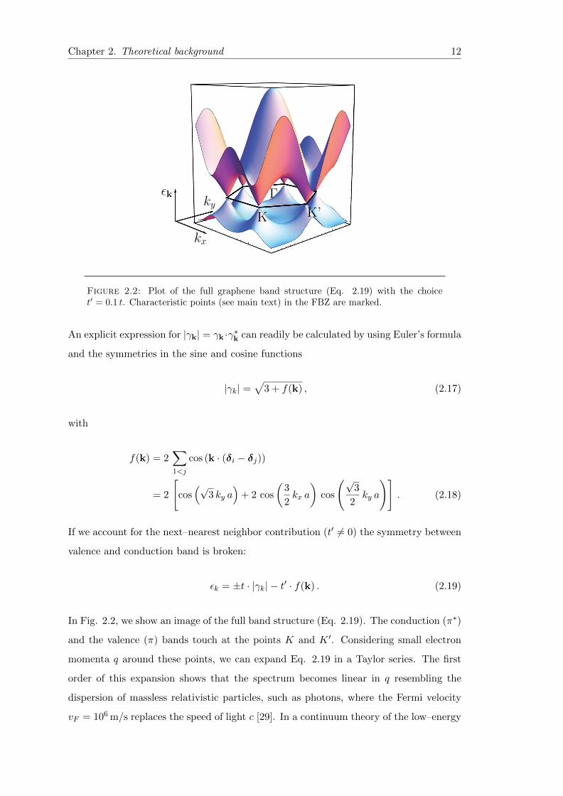
K K’
Γεk
kx
ky
Figure 2.2: Plot of the full graphene band structure (Eq. 2.19) with the choicet′ = 0.1 t. Characteristic points (see main text) in the FBZ are marked.
An explicit expression for |γk| = γk ·γ∗k can readily be calculated by using Euler’s formula
and the symmetries in the sine and cosine functions
|γk| =√
3 + f(k) , (2.17)
with
f(k) = 2∑1<j
cos (k · (δi − δj))
= 2
[cos(√
3 ky a)
+ 2 cos
(3
2kx a
)cos
(√3
2ky a
)]. (2.18)
If we account for the next–nearest neighbor contribution (t′ 6= 0) the symmetry between
valence and conduction band is broken:
εk = ±t · |γk| − t′ · f(k) . (2.19)
In Fig. 2.2, we show an image of the full band structure (Eq. 2.19). The conduction (π∗)
and the valence (π) bands touch at the points K and K ′. Considering small electron
momenta q around these points, we can expand Eq. 2.19 in a Taylor series. The first
order of this expansion shows that the spectrum becomes linear in q resembling the
dispersion of massless relativistic particles, such as photons, where the Fermi velocity
vF = 106 m/s replaces the speed of light c [29]. In a continuum theory of the low–energy
Chapter 2. Theoretical background 13
excitations it can be shown that a two–dimensional Dirac equation is able to describe
the physics in this regime appropriately [29, 43]. This result is also robust towards the
influence of next–nearest neighbor hopping because all further corrections lead to higher
order terms in the expansion beyond the dominating linear one [44].
2.2.2 Turbostratic graphene multilayers
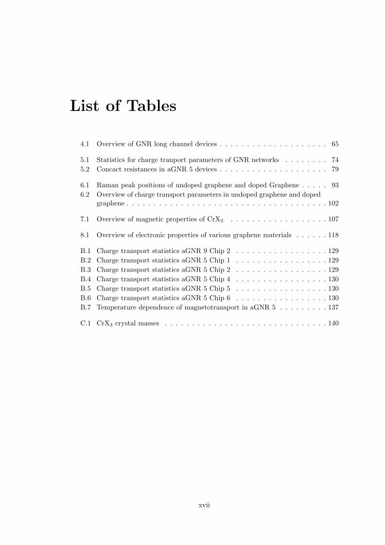
The unusual electronic structure of graphene monolayers as discussed in the previous
section is altered when graphene layers are stacked and form bi– or multilayer systems.
However, the stacking order is crucial as it determines in which way the electronic
properties change [29]. Starting with a first graphene layer (A) at a fixed position, a
second layer (B) is usually displaced by a nearest neighbour vector of the honeycomb
lattice δi, i = 1, 2, 3 (see Eq. 2.9). As a consequence of this translation, half of the
atoms in B are directly above the atoms of one sublattice of A and the other half sits
on top of the hexagon centers of the first layer as depicted in Fig. 2.3 (a). To describe
the electronic properties of such bilayer graphene, further tight–binding parameters can
be introduced to the model Hamiltonian in Eq. 2.14 in order to account for interlayer
hopping. The adapted model leads to a quadratic energy dispersion around the K points
instead of the linear Dirac cone [29] and this result does not depend on the choice of δi
for the translation of the second layer. However, stacks with a large number of layers
can be arbitrarily complex in their stacking order and analytical expressions for the
electronic bands can only be obtained for the highly ordered cases. In the most common
arrangement the sign of the translation alternates, i.e. δi, −δi, δi, −δi, . . . leading
to ABA or Bernal stacking (α-graphite). Here, the established model for the band
structure was developed by Slonceswki and Weiss [45] and McClure [46] which does not
give rise to the massless Dirac fermions of graphene monolayers. Nevertheless, there is a
way to preserve the linear dispersion around the Dirac point, which is by introducing a
twist angle between adjacent graphene layers, so–called turbostratic graphene (TG) [47].
From a theoretical point of view, the constant rotation of graphene layers with respect
to adjacent ones leads to the restoration of the fourfold band-structure degeneracy at the
Dirac point with an energy interval around it, where the linear dispersion is kept intact.
The superlattice, which is a moire lattice as exemplified in Fig. 2.3 (b), is characterized
by the rotation angle ϕ which therefore is crucial for the electronic properties. The
rotation angle can be calculating using the lattice vector of the unrotated layer a1 and
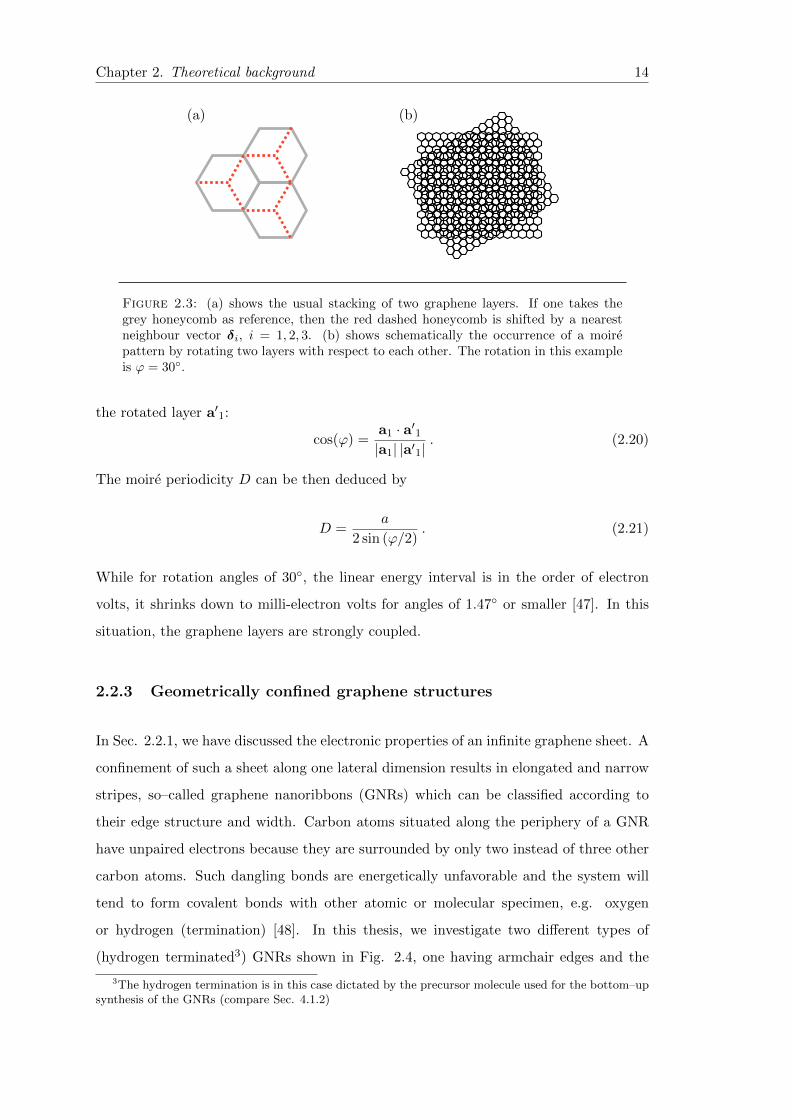
Chapter 2. Theoretical background 14
(a) (b)
Figure 2.3: (a) shows the usual stacking of two graphene layers. If one takes thegrey honeycomb as reference, then the red dashed honeycomb is shifted by a nearestneighbour vector δi, i = 1, 2, 3. (b) shows schematically the occurrence of a moirepattern by rotating two layers with respect to each other. The rotation in this exampleis ϕ = 30.
the rotated layer a′1:
cos(ϕ) =a1 · a′1|a1| |a′1|
. (2.20)
The moire periodicity D can be then deduced by
D =a
2 sin (ϕ/2). (2.21)
While for rotation angles of 30, the linear energy interval is in the order of electron
volts, it shrinks down to milli-electron volts for angles of 1.47 or smaller [47]. In this
situation, the graphene layers are strongly coupled.
2.2.3 Geometrically confined graphene structures
In Sec. 2.2.1, we have discussed the electronic properties of an infinite graphene sheet. A
confinement of such a sheet along one lateral dimension results in elongated and narrow
stripes, so–called graphene nanoribbons (GNRs) which can be classified according to
their edge structure and width. Carbon atoms situated along the periphery of a GNR
have unpaired electrons because they are surrounded by only two instead of three other
carbon atoms. Such dangling bonds are energetically unfavorable and the system will
tend to form covalent bonds with other atomic or molecular specimen, e.g. oxygen
or hydrogen (termination) [48]. In this thesis, we investigate two different types of
(hydrogen terminated3) GNRs shown in Fig. 2.4, one having armchair edges and the
3The hydrogen termination is in this case dictated by the precursor molecule used for the bottom–upsynthesis of the GNRs (compare Sec. 4.1.2)
Chapter 2. Theoretical background 15
other exhibiting a so–called chevron structure. The electronic properties of a GNR
depend crucially on both, its width and its edge structure, and various techniques have
been invoked to calculate the energy bands, such as the tight–binding method [5, 41, 49,
50], solutions of the Dirac equation [51–53] as well as density functional theory (DFT)
and ab initio calculations [41, 54–57]. However, all solutions have in common that
they must satisfy the boundary conditions dictated by the GNR structure, namely the
electron wave function vanishes at the borders of the ribbon.
2.2.3.1 Armchair and zigzag GNRs
In the hexagonal graphene lattice, there are two distinct types of edges, armchair and
zigzag, which are formed when we imagine the lattice to be cut along certain directions. If
we choose the horizontal x–axis in Fig. 2.1 to mark zero degrees, we find armchair edges
at angles θa = 0, 60 and 120, while we can follow a zigzag edge at angles θz = 30,
90 and 150. The electronic properties of armchair GNRs (aGNRs) are remarkebly
different from those of zigzag GNRs (zGNRs) and both show clear distinctions to the
electronic structure of an extended graphene sheet. Especially, zGNRs host localized
electronic edge states with energies close to the Fermi level EF residing exclusively on
one sublattice and absent in two–dimensional graphene as well as in aGNRs [5, 49, 50].
Their existence can be demonstrated for example analytically, considering a semi–infinite
graphene sheet with a zigzag edge, or on the level of a nearest–neighbor tight binding
ansatz for the π electrons [29, 49, 53]. As a consequence of these states, particular
features in the energy spectrum and the DOS emerge. The highest valence band and
the lowest conduction band are associated to the edge states and become (partially) flat
in the region 2π/3 ≤ k ≤ π. Even on the basis of more sophisticated calculations, these
bands are degenerate as long as the spin degree of freedom is not considered, rendering
zGNRs generally metallic [54–56]. Such flat bands are linked to a sharp increase of the
DOS around EF which is in contrast to the non–confined case, where the DOS vanishes
at EF . With this enhanced DOS, magnetic ordering of electron spins has been predicted
where the coupling is ferromagnetic along one edge and antiferromagnetic for opposite
edges [49, 58–61]. A staggered potential resulting from the magnetic ordering can lift
the degeneracy of the flat band in the antiferromagnetic ground state and a band gap
opens up, while a state where spins on opposite edges are parallel remains metallic
[6, 54, 58, 62, 63]. However, at finite temperatures, a long range magnetic order is not
Chapter 2. Theoretical background 16
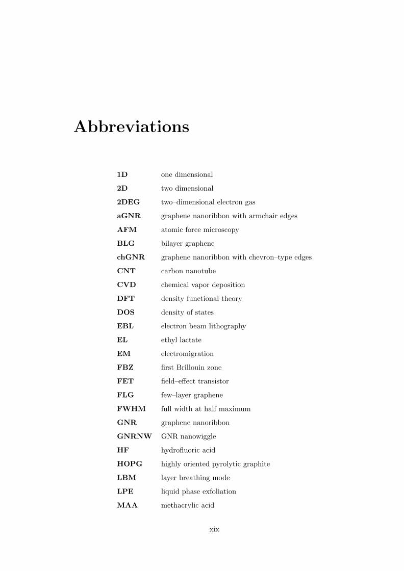
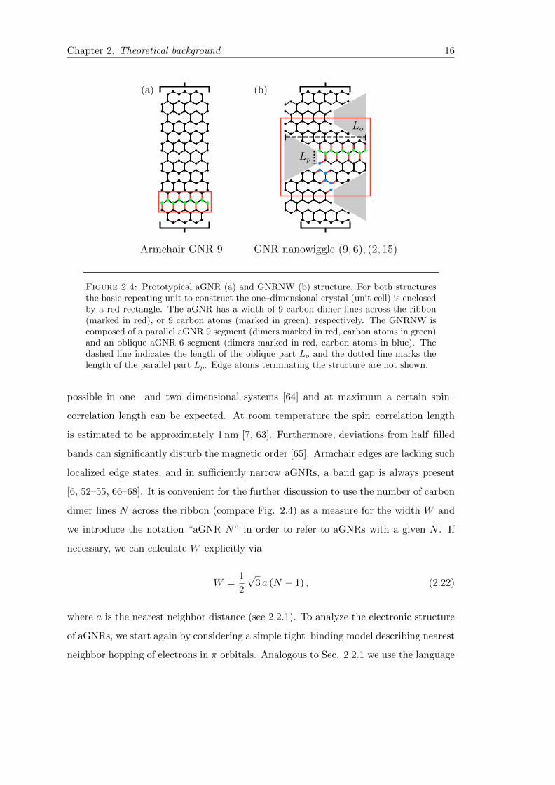
(a) (b)
Armchair GNR 9 GNR nanowiggle (9, 6), (2, 15)
Lp
Lo
Figure 2.4: Prototypical aGNR (a) and GNRNW (b) structure. For both structuresthe basic repeating unit to construct the one–dimensional crystal (unit cell) is enclosedby a red rectangle. The aGNR has a width of 9 carbon dimer lines across the ribbon(marked in red), or 9 carbon atoms (marked in green), respectively. The GNRNW iscomposed of a parallel aGNR 9 segment (dimers marked in red, carbon atoms in green)and an oblique aGNR 6 segment (dimers marked in red, carbon atoms in blue). Thedashed line indicates the length of the oblique part Lo and the dotted line marks thelength of the parallel part Lp. Edge atoms terminating the structure are not shown.
possible in one– and two–dimensional systems [64] and at maximum a certain spin–
correlation length can be expected. At room temperature the spin–correlation length
is estimated to be approximately 1 nm [7, 63]. Furthermore, deviations from half–filled
bands can significantly disturb the magnetic order [65]. Armchair edges are lacking such
localized edge states, and in sufficiently narrow aGNRs, a band gap is always present
[6, 52–55, 66–68]. It is convenient for the further discussion to use the number of carbon
dimer lines N across the ribbon (compare Fig. 2.4) as a measure for the width W and
we introduce the notation “aGNR N” in order to refer to aGNRs with a given N . If
necessary, we can calculate W explicitly via
W =1
2
√3 a (N − 1) , (2.22)
where a is the nearest neighbor distance (see 2.2.1). To analyze the electronic structure
of aGNRs, we start again by considering a simple tight–binding model describing nearest
neighbor hopping of electrons in π orbitals. Analogous to Sec. 2.2.1 we use the language
Chapter 2. Theoretical background 17
of second quantization to set up an appropriate model Hamiltonian [69]:
H = −t∑l
[ ∑m∈odd
a†l (m)bl−1(m) +∑
m∈even
a†l (m+ 1)
]+ H.c.
− t∑l
N−1∑m=1
[b†l (m+ 1)al(m) + a†l (m+ 1)bl(m)
]+ H.c. . (2.23)
Herein, al(m) and bl(m) (a†l (m) and b†l (m)) are the annihilation (creation) operators
of an electron at sublattice site A and B of the mth dimer and in the lth unit cell.
The first line describes hopping of electrons along the ribbon (longitudinal) while the
second line accounts for hopping across the ribbon (transverse). Wakabayashi et al.
provide a detailed calculation of the eigenvalues for Eq. 2.23 in Ref. [69] and here, we
just summarize the result. The boundary conditions lead to the discretization of the
electron momentum in the transverse direction:
p =r π
N + 1, r = 1, 2, . . . , N , (2.24)
while the longitudinal momentum k is continuous for infinitely long ribbons. The spec-
trum can be derived explicitly:
E = ±t
√1 + 4
(cos (p) cos
(k
2
)+ cos2 (p)
). (2.25)
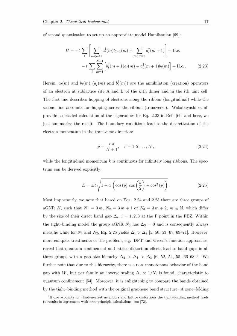
Most importantly, we note that based on Eqs. 2.24 and 2.25 there are three groups of
aGNR N , such that N1 = 3m, N2 = 3m + 1 or N3 = 3m + 2, m ∈ N, which differ
by the size of their direct band gap ∆i, i = 1, 2, 3 at the Γ point in the FBZ. Within
the tight–binding model the group aGNR N3 has ∆3 = 0 and is consequently always
metallic while for N1 and N2, Eq. 2.25 yields ∆1 > ∆2 [5, 50, 53, 67, 69–71]. However,
more complex treatments of the problem, e.g. DFT and Green’s function approaches,
reveal that quantum confinement and lattice distortion effects lead to band gaps in all
three groups with a gap size hierachy ∆2 > ∆1 > ∆3 [6, 52, 54, 55, 66–68].4 We
further note that due to this hierarchy, there is a non–monotonous behavior of the band
gap with W , but per family an inverse scaling ∆i ∝ 1/Ni is found, characteristic to
quantum confinement [54]. Moreover, it is enlightening to compare the bands obtained
by the tight–binding method with the original graphene band structure. A zone–folding
4If one accounts for third–nearest neighbors and lattice distortions the tight–binding method leadsto results in agreement with first–principle calculations, too [72].
Chapter 2. Theoretical background 18
0
0
-1.5
-3
1.5
3
1-1
0
-1.5
-3
1.5
3
0 1-1
0
1.5
3
0 1
-1.5
-3
-1
E/t
E/t
E/t
kx a kx a kx a
N = 5 N = 9 N = 30
Figure 2.5: Tight–binding energy bands of aGNR 5, aGNR 9 and aGNR 30. Whilethe N = 5 ribbon is metallic, there is a gap in the N = 9 and N = 30 cases. Theprojected valence band (blue) and conduction band (red) of a two–dimensional extendedgraphene sheet are shown in each plot as colored overlay, illustrating the agreement ofthe dispersions in the limit N →∞.
technique can be applied, where we project the two–dimensional graphene band strucutre
(Eq. 2.16) onto the armchair direction in the hexagonal FBZ (see Fig. 2.5) [5, 69, 70].
The linear dispersion around the K point gives rise to the valence band and conduction
band of the aGNR touching at k = 0 in the one–dimensional FBZ. On the other hand,
towards the borders of the FBZ, the bands move apart leading to large gaps at k = ±π.
As discussed, the direct gap opens in the FBZ central region for small N , while for large
N , the resemblance to the projection becomes more and more obvious (see Fig 2.5).
2.2.3.2 Chevron GNRs
Besides the regular armchair and zigzag edge patterns, more complicated morphologies
are possible, for example by fusing armchair or zigzag segments in a kinked fashion, by
introducing a chirality or by adding (periodic) functionalizations along the edge. In this
way, GNRs with cove–type edges [73, 74], chiral GNRs [75–78], or chevron–like GNRs
(chGNRs) [79–82] can be obtained. The latter comprises a multitude of subclasses with
structural variations, such as jagged GNRs [83], sawtooth GNRs [84], W–shaped GNRs
[85], or so–called nanowiggles [86], and theory predicts intriguing thermoelectric [87, 88]
electronic and magnetic properties [81, 86] resulting from the non–straight topologies.
The fundamental difference of fused GNR blocks of different width and straight GNRs is
Chapter 2. Theoretical background 19
Ener
gy(e
V)
Momentum along ribbon axis (2 π/d)
Figure 2.6: Energy bands of GNRNW (9, 6), (2, 15) obtained by DFT calculations.The symbol d denotes the length of the unit cell in real space. Adapted and reprintedby permission from Macmillan Publishers Ltd: Nature 466, 470. Copyright 2010 (Ref.[79]).
the occurence of a new periodicity in the system, which defines a superlattice. Superlat-
tices can lead to a strong modulation of the energy gap in real space resulting in quantum
well structures or series of quantum dots [89]. Hence, designing the periodicity of the
superlattice opens up another opportunity to tailor the electronic properties of GNRs
[88, 90] as it has been done very successfully in conventional semiconductors [91, 92].
Due to the aformentioned variety of structures there is no general classification scheme
covering all possible chGNRs. Only within chGNR subfamilies certain regularities can
be found such that often a small number of parameters defines the ribbons contained in
the respective subfamily.
Here, we focus on GNR nanowiggles (GNRNWs) with lattice structures which can be
viewed from two different perspectives. On the one hand, we can describe them as
successive repetitions of parallel and oblique aGNR and/or zGNR segments, seamlessly
stitched together. On the other hand, we can imagine a wide aGNR/zGNR from which
trapezoidal wedges are carved out on alternating edges. The GNRNW structure depicted
in Fig. 2.4 is the relevant one for this thesis and it is assembled from two aGNR segments
of different width. To exemplify the alternative picture, we mark the “removed” parts of
a wide GNR as shaded areas in Fig. 2.4 as well. A set of four parameters is uniquely as-
sociated with any allowed GNRNW structure, if certain regularity conditions are applied
[86]. These parameters are the lengths (Lp, Lo) and the widths (Wp,Wo) of the parallel
Chapter 2. Theoretical background 20
and the oblique domains, respectively. For the width of each segment we count the car-
bon dimer lines in the usual way and obtain (Wp,Wo) = (9, 6). The length Lo is defined
as the width of the (imaginary) wedge–healed aGNR and the length Lp is the num-
ber of carbon–carbon distances a expanding along the smallest basis of the trapezoids,
which yields Lo = 15 and Lp = 2 for our case. The electronic structure of GNRNWs
is accurately described in the tight–binding framework [86]. However, the majority of
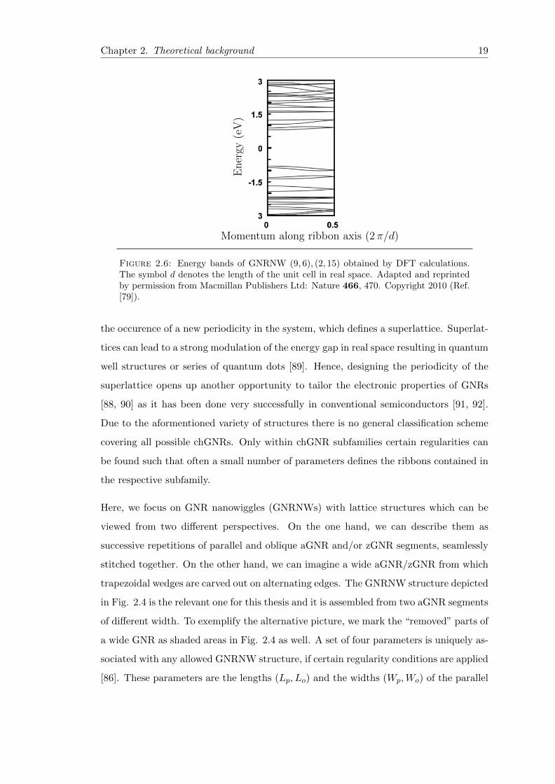
calculations available in literature are based on first principles. In Fig. 2.6, we show an
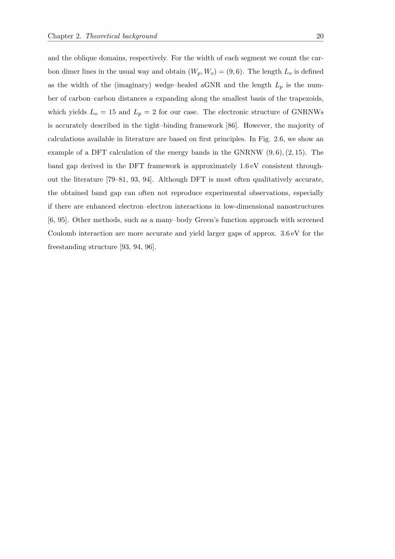
example of a DFT calculation of the energy bands in the GNRNW (9, 6), (2, 15). The
band gap derived in the DFT framework is approximately 1.6 eV consistent through-
out the literature [79–81, 93, 94]. Although DFT is most often qualitatively accurate,
the obtained band gap can often not reproduce experimental observations, especially
if there are enhanced electron–electron interactions in low-dimensional nanostructures
[6, 95]. Other methods, such as a many–body Green’s function approach with screened
Coulomb interaction are more accurate and yield larger gaps of approx. 3.6 eV for the
freestanding structure [93, 94, 96].
Chapter 2. Theoretical background 21
2.3 Charge transport by charge carrier hopping
In disordered solids like polycrystalline or amorophous (organic as well as inorganic)
semiconductors the wavefunction of charge carriers is not delocalized over the whole vol-
ume. In this case, transport of charge carriers is dominated by the transition between
localized sites via tunneling or overcoming potential barriers instead of the wave–like
propagation found in crystalline and structurally ordered materials. The hopping tran-
sition rate kij from an occupied site i to an empty site j is typically described either
by the Miller–Abrahams formalism or by Marcus theory [97–99]. However, the theory
of nuclear tunneling, which is based on tunneling in an asymmetrically biased double
quantum well, is able to give a unified description of charge transport in virtually all
important organic semiconductors [100, 101]. Here, the nuclear vibrations are coupled
to the charges and drive the charge transfer from site to site. Assuming a purely dissipa-
tive situation, Fisher and Dorsey, and Grabert and Weiss [102, 103] derived an analytic
expression for the transfer rate
kij =H2
ij
~2 ωc
(~ωc
2π kB T
)1−2α∗ ∣∣∣∣Γ(α∗ + i
(εij
2π kB T
))∣∣∣∣2× Γ(2α∗)−1 exp
(εij
2 kB T
)exp
(− |εij |~ωc
),
(2.26)
where Hij is the electronic coupling between initial and final state, εij is the difference
in energy between donor and acceptor states, α∗ is the Kondo parameter describing the
coupling strength between charge and bath, ωc is the characteristic frequency of the
bath, kB is the Boltzmann constant, T is the temperature and Γ is the complex gamma
function. Following the considerations in Ref. [100], the macroscopic electric current in
such a system can be calculated based on Eq. 2.26 by comparing forward and backward
hopping events
I ∝ kforward − kbackward = k(εij)− k(−εij) . (2.27)
Under the assumption of equal hopping steps, the energy difference of the states i and j
in Eq. 2.27 can be written in terms of the applied bias potential V , the hopping distance
Lij and the total distance L which the charge carrier has to traverse
εij = Lij e V/L = γ e V , (2.28)
Chapter 2. Theoretical background 22
where we define γ−1 = L/Lij as the number of hopping events performed by charge
carriers to cover the full distance between the electrodes and e is the elementary charge.
We now substitute Eqs. 2.26 and 2.28 into Eq. 2.27, define α = 2 (α∗ − 1) and consider
the limit |εij | ≤ ~ωc. This yields an analytic formula for the expected current density
[100]
J = J0 T1+α sinh
(γ e V
2 kB T
) ∣∣∣∣Γ(1 +α
2+ i
γ e V
2π kB T
)∣∣∣∣2 . (2.29)
There are two limiting cases that can be drawn from Eq. 2.29: In the low–voltage Ohmic
range, the current density is given by
limV→0
J =J0 γ e
2 kB T
∣∣∣Γ(1 +α
2
)∣∣∣2 Tα V . (2.30)
Furthermore, the opposite limit of high voltages results in a temperature independent
power law for the current density
limV→∞
J = J0 π−α(γ e
2 kB
)βV β . (2.31)
Within the framework of nuclear tunneling theory, the exponents α and β of Eqs. 2.30
and 2.31 are connected as β = α+1. Equations 2.29, 2.30 and 2.31 play important roles
in the analysis of charge transport in Sec. 5. Furthermore, the charge carrier mobility
in hopping systems can be approximated using a modified Einstein relation [104]
µ =e a2
kB Tk , (2.32)
where a is the intermolecular (hopping) distance and k is the charge transfer or hopping
probability per unit time. Equation 2.32 shows clearly, that the mobility in the case
of hopping is governed by the hopping rate in contrast to the case of delocalized band
transport, where the mobility scales with the average scattering time τ [105]. As a
consequence, the mobility is typically much lower in hopping systems than in crystalline
systems [104].
Chapter 2. Theoretical background 23
2.4 Basics of magnetism
In Sec. 7 of this thesis, we investigate the magnetic properties of chromium trihalo-
genides, a class of layered materials. The following paragraphs summarize briefly the
most important concepts to understand magnetism in solids. Magnetic phenomena arise
due to the subtle and complex interplay of elementary magnetic moments. These mag-
netic moments are caused by the electron’s angular momentum that is comprised of the
electron’s orbital motion and its spin. The angular momentum and the magnetic dipole
moment of electrons are linked as follows:
µ = −µB~
(L + gS) . (2.33)
In Eq. 2.33, µB = e ~/2me denotes the Bohr magneton with me the electron mass. The
g–factor is g ≈ 2 for the electron [106]. The dipolar fields created by these moments are
typically too weak to account for long range magnetic order and only so–called exchange
interactions, based on quantum mechanical principles, lead to the ordering of magnetic
moments [106].
2.4.1 Direct exchange
Arising from Pauli’s exclusion principle for fermions, exchange is a purely quantum
mechanical phenomenon. The spins of electrons with wavefunctions ψa (r1) and ψb (r2)
located at positions r1 and r2 can either couple into a singlet (S = 0) or a triplet
state (S = 1), which implies that the spin configuration is either antiparallel or parallel,
respectively. Depending on the energy difference between both states, one or the other
alignment will be preferred [106]
Ja,b = ES − ET = 2
∫ψ∗a (r1)ψ∗b (r2) Hψa (r2)ψb (r1) dr1dr2 . (2.34)
The symbol ψ∗a/b denotes the complex conjugate of the wave function. If Ja,b > 0, we
have ES > ET and the triplet state is favoured. In a (magnetic) solid an interaction of
the form Eq. 2.34 applies between all neighboring spins and a general Hamiltonian can
be written as [106]
H = −∑i,j
Ji,jSiSj . (2.35)
Chapter 2. Theoretical background 24
2.4.2 Itinerant ferromagnetism
In some cases magnetic order in metals is associated with delocalised 3d–electrons
that move freely through the material (itinerant electrons). If it becomes energet-
ically favorable for some electrons with energies within ∆E around the Fermi edge
to flip their spin from down to up and thus create an imbalance in the spin popula-
tion, ferromagnetic ordering is established [106]. The new densities are then given by
n↑/↓ = 1/2 (n± g (EF ) ∆E) with g (EF ) the density of states at the Fermi level. This
gives rise to a net magnetization M = µB (n↑ − n↓) 6= 0.
In this situation two energy terms are competing. On the one hand the electrons gain
kinetic energy Ekin = 12g (EF ) (∆E)2. On the other hand there is also a reduction of
energy which is due to the interaction of the magnetization with the molecular field:
Epot = −∫ M
0µ0λM
′dM ′ = −1
2µ0λM
2 . (2.36)
The parameter λ expresses how large a molecular field is obtained for a given magnetiza-
tion. The quantity U = µ0µ2Bλ is then a measure of the Coulomb energy. The condition
for ferromagnetism becomes
Ekin + Epot =1
2g (EF ) (∆E)2 (1− Ug (EF )) ≤ 0 , (2.37)
which leads to the so–called Stoner criterion for ferromagnetism [107]
U g (EF ) ≥ 1 . (2.38)
Hence, ferromagnetism requires strong Coulomb effects and a high density of states at
the Fermi energy.
2.4.3 Superexchange
The term “superexchange” describes the phenomenon of magnetically coupled cations,
whose interaction is mediated by an anion. In such cases, the spatial distance between
the cations is large, typically in the order of Angstroms, and several atomic orbitals are
involved. The concepts and the theory behind this phenomenon have been introduced
Chapter 2. Theoretical background 25
first by H. Kramers [108], and were then fully developed mainly by P. W. Anderson [109–
111], J. B. Goodenough [112, 113] and J. Kanamori [114]. The superexchange effect in
ionic insulators, with the antiferromagnet MnO being one of the most famous examples,
can be derived from quantum mechanical perturbation theory in a one–electron Hartree–
Fock approach. This electron is considered to be the “magnetic” electron, typically
occupying a d shell, while all other, s and p, electrons are core electrons. An intermixing
of the magnetic d electron wave with the p electron wave of the non–magnetic anion
is then the primary mechanism of superexchange [115]. If the magnetic electron is
delocalized over the whole structure it has the chance to lower its kinetic energy (at the
cost of Coulomb energy U). The exchange constant is then
J ∝ −b2
U, (2.39)
where b denotes the electron transfer integral accounting for its kinetic energy [115]. In
general, superexchange leads to antiferromagnetic coupling and only in rare cases ferro-
magnetic coupling occurs. A set of semi–empirical rules were developed by Goodenough
and Kanamori which are very useful to rationalize the magnetic properties of superex-
change coupled materials on a qualitative level [112–114]. We summarize these rules in
the form given by Anderson in Ref. [115]. In order to predict the magnetic coupling in
an ionic material, one firstly determines which of the d orbitals contains the magnetic
electrons according to ligand field theory. The two rules are then:
A. Two ions with magnetic orbital lobes pointing towards each other in such a way
that the orbitals would have a large overlap integral, the superexchange is antifer-
romagnetic. Herein, we can find three subcases:
1. The lobes are of dz2–type in the octahedral case and they are in a 180
position, such that they point directly toward the mediating anion and toward
each other. Then the antiferromagnetic superexchange interaction is large.
2. The lobes are of dxy–type and are in a 180 position. Then the antiferromag-
netic superexchange interaction is large.
3. On one ion, the electron occupies a dz2 orbital and on the other ion, the
electron occupies a dxy orbital and they are in a 90 position. Then the
pπ orbital is the pσ for the other and the antiferromagnetic superexchange
interaction is large
Chapter 2. Theoretical background 26
B. The magnetic orbitals are arranged such that they are in contact but the overlap
integral is comparatively small. This would be the case if on one ion, the electron
occupies a dz2 orbital and on the other ion, the electron occupies a dxy orbital and
they are in a 180 position. Then the ferromagnetic superexchange interaction is
large (nevertheless, not as strong as the antiferromagnetic one in the other cases).
Chapter 3
Experimental methods
For the characterization of the materials investigated within this thesis, a multitude
of experimental methods were employed. This chapter introduces the most important
techniques which were used to access and quantify structural and electrical properties
of these materials. We begin with Raman spectroscopy, which is a powerful tool to
determine the structural integrity of carbon materials. Furthermore, charge transport
measurements at variable temperatures and high magnetic fields require dedicated se-
tups, which involve helium cryostats, superconducting magnets and appropriate source–
measure devices. In order to extract material specific quantities, such as resistivity or
charge carrier mobility, the geometry of the current path must be known or the van der
Pauw (VDP) method must be applied. Finally, the magnetic properties of chromium
trihalides were determined by a superconducting quantum interference device (SQUID).
3.1 Structural characterization by Raman spectroscopy
Raman spectroscopy [116] is one of the most common techniques to characterize the
structure of graphene–based systems. It can be used to unambigiuously identify CNTs,
single and multilayer graphene and GNRs based on their specific Raman spectra, which
serve as unique fingerprints [117]. Raman spectroscopy relies on the (inelastic) Raman
scattering [118, 119] of photons (with an energy of ~ω) in a crystal under the creation
or annihilation of excitations such as phonons or magnons (with energy ~Ω). The scat-
tering generally involves intermediary electronic states. If the incoming photon creates
27
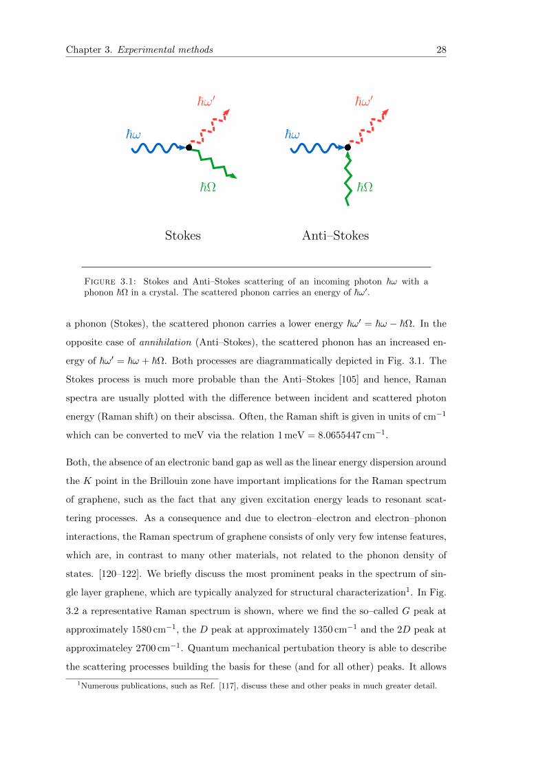
Chapter 3. Experimental methods 28
Stokes Anti–Stokes
~ω
~ω′
~Ω
~ω
~ω′
~Ω
Figure 3.1: Stokes and Anti–Stokes scattering of an incoming photon ~ω with aphonon ~Ω in a crystal. The scattered phonon carries an energy of ~ω′.
a phonon (Stokes), the scattered phonon carries a lower energy ~ω′ = ~ω − ~Ω. In the
opposite case of annihilation (Anti–Stokes), the scattered phonon has an increased en-
ergy of ~ω′ = ~ω + ~Ω. Both processes are diagrammatically depicted in Fig. 3.1. The
Stokes process is much more probable than the Anti–Stokes [105] and hence, Raman
spectra are usually plotted with the difference between incident and scattered photon
energy (Raman shift) on their abscissa. Often, the Raman shift is given in units of cm−1
which can be converted to meV via the relation 1 meV = 8.0655447 cm−1.
Both, the absence of an electronic band gap as well as the linear energy dispersion around
the K point in the Brillouin zone have important implications for the Raman spectrum
of graphene, such as the fact that any given excitation energy leads to resonant scat-
tering processes. As a consequence and due to electron–electron and electron–phonon
interactions, the Raman spectrum of graphene consists of only very few intense features,
which are, in contrast to many other materials, not related to the phonon density of
states. [120–122]. We briefly discuss the most prominent peaks in the spectrum of sin-
gle layer graphene, which are typically analyzed for structural characterization1. In Fig.
3.2 a representative Raman spectrum is shown, where we find the so–called G peak at
approximately 1580 cm−1, the D peak at approximately 1350 cm−1 and the 2D peak at
approximateley 2700 cm−1. Quantum mechanical pertubation theory is able to describe
the scattering processes building the basis for these (and for all other) peaks. It allows
1Numerous publications, such as Ref. [117], discuss these and other peaks in much greater detail.
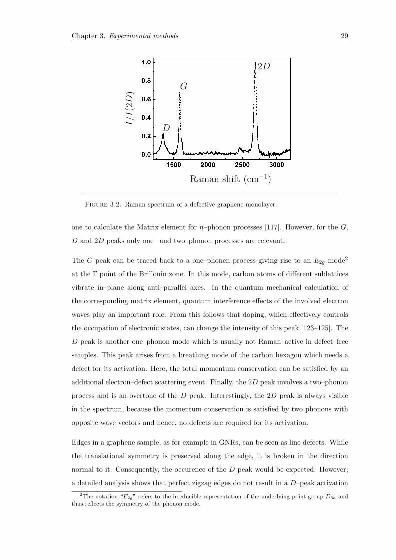
Chapter 3. Experimental methods 29
Raman shift (cm−1)
I/I
(2D
)D
G
2D
Figure 3.2: Raman spectrum of a defective graphene monolayer.
one to calculate the Matrix element for n–phonon processes [117]. However, for the G,
D and 2D peaks only one– and two–phonon processes are relevant.
The G peak can be traced back to a one–phonen process giving rise to an E2g mode2
at the Γ point of the Brillouin zone. In this mode, carbon atoms of different sublattices
vibrate in–plane along anti–parallel axes. In the quantum mechanical calculation of
the corresponding matrix element, quantum interference effects of the involved electron
waves play an important role. From this follows that doping, which effectively controls
the occupation of electronic states, can change the intensity of this peak [123–125]. The
D peak is another one–phonon mode which is usually not Raman–active in defect–free
samples. This peak arises from a breathing mode of the carbon hexagon which needs a
defect for its activation. Here, the total momentum conservation can be satisfied by an
additional electron–defect scattering event. Finally, the 2D peak involves a two–phonon
process and is an overtone of the D peak. Interestingly, the 2D peak is always visible
in the spectrum, because the momentum conservation is satisfied by two phonons with
opposite wave vectors and hence, no defects are required for its activation.
Edges in a graphene sample, as for example in GNRs, can be seen as line defects. While
the translational symmetry is preserved along the edge, it is broken in the direction
normal to it. Consequently, the occurence of the D peak would be expected. However,
a detailed analysis shows that perfect zigzag edges do not result in a D–peak activation
2The notation “E2g” refers to the irreducible representation of the underlying point group D6h andthus reflects the symmetry of the phonon mode.
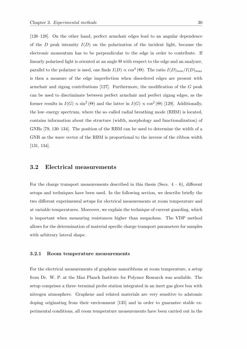
Chapter 3. Experimental methods 30
[126–128]. On the other hand, perfect armchair edges lead to an angular dependence
of the D peak intensity I(D) on the polarization of the incident light, because the
electronic momentum has to be perpendicular to the edge in order to contribute. If
linearly polarized light is oriented at an angle Θ with respect to the edge and an analyzer,
parallel to the polarizer is used, one finds I(D) ∝ cos4 (Θ). The ratio I(D)min/I(D)max
is then a measure of the edge imperfection when disordered edges are present with
armchair and zigzag contributions [127]. Furthermore, the modification of the G peak
can be used to discriminate between perfect armchair and perfect zigzag edges, as the
former results in I(G) ∝ sin2 (Θ) and the latter in I(G) ∝ cos2 (Θ) [129]. Additionally,
the low–energy spectrum, where the so–called radial breathing mode (RBM) is located,
contains information about the structure (width, morphology and functionalization) of
GNRs [79, 130–134]. The position of the RBM can be used to determine the width of a
GNR as the wave vector of the RBM is proportional to the inverse of the ribbon width
[131, 134].
3.2 Electrical measurements
For the charge transport measurements described in this thesis (Secs. 4 – 6), different
setups and techniques have been used. In the following section, we describe briefly the
two different experimental setups for electrical measurements at room temperature and
at variable temperatures. Moreover, we explain the technique of current guarding, which
is important when measuring resistances higher than megaohms. The VDP method
allows for the determination of material specific charge transport parameters for samples
with arbitrary lateral shape.
3.2.1 Room temperature measurements
For the electrical measurements of graphene nanoribbons at room temperature, a setup
from Dr. W. P. at the Max Planck Institute for Polymer Research was available. The
setup comprises a three–terminal probe station integrated in an inert gas glove box with
nitrogen atmosphere. Graphene and related materials are very sensitive to adatomic
doping originating from their environment [135] and in order to guarantee stable ex-
perimental conditions, all room temperature measurements have been carried out in the
Chapter 3. Experimental methods 31
Guard 1
Signal 1
Guard 2
Signal 2
Guard 3
Signal 3
Guard 4
Signal 4
Figure 3.3: Cryostat sample holder suitable for the measurement of highly resistivesamples. Since the holder is designed for guarded measurements using triaxial connec-tions, it has four signal pins and additionally four guard pins (see Sec. 3.2.3).
glove box. Typically, the glove box contains ≤ 3 ppm of molecular oxygen and ≤ 0.1 ppm
of water. The probe station is connected to a Keithley 4200 semiconductor character-
ization system which contains three independent source–measure units and allows for
the electrical characterization of test devices.
3.2.2 Low temperature measurements
Variable temperature measurements have been carried out in a bath cryostat equipped
with a dynamic variable temperature insert (VTI) at the bottom of the sample space
which allows for the control of the sample temperature. Stable temperatures within
approx. 0.1 K are obtained by balancing the cooling power of a liquid helium flow
against the heating power of a electrical resistive heating element. The liquid helium
is drawn from the main reservoir through a needle valve which is adjusted manually.
Temperatures below 4.2 K are obtained by reducing the vapour pressure of the liquid
helium in the sample space by mechanical pumping. Furthermore, the setup contains
a superconducting magnet, capable of applying unidirectional magnetic fields up to
9 T. Electrical measurements are enabled with a Keithley 238 source–measure unit or
using a combination of a Keithley 224 current source and a Keithley 182 voltmeter. A
measurement computer allows for a remote control of the setup. While in a probe station
setup as in the room temperature measurements metallic needles establish an electrical
connection positioned on the sample surface with the help of micromanipulators, for
measurements in the cryostat, the sample has to be glued to a sample holder. In Fig.
3.3 a sample holder is shown, which has four signal connections each protected by a
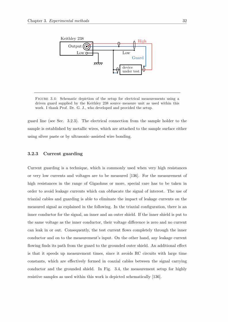
Chapter 3. Experimental methods 32
Keithley 238
Output
Low
High
GuardLow
deviceunder test
Figure 3.4: Schematic depiction of the setup for electrical measurements using adriven guard supplied by the Keithley 238 source–measure unit as used within thiswork. I thank Prof. Dr. G. J., who developed and provided the setup.
guard line (see Sec. 3.2.3). The electrical connection from the sample holder to the
sample is established by metallic wires, which are attached to the sample surface either
using silver paste or by ultrasonic–assisted wire bonding.
3.2.3 Current guarding
Current guarding is a technique, which is commonly used when very high resistances
or very low currents and voltages are to be measured [136]. For the measurement of
high resistances in the range of Gigaohms or more, special care has to be taken in
order to avoid leakage currents which can obfuscate the signal of interest. The use of
triaxial cables and guarding is able to eliminate the impact of leakage currents on the
measured signal as explained in the following. In the triaxial configuration, there is an
inner conductor for the signal, an inner and an outer shield. If the inner shield is put to
the same voltage as the inner conductor, their voltage difference is zero and no current
can leak in or out. Consequently, the test current flows completely through the inner
conductor and on to the measurement’s input. On the other hand, any leakage current
flowing finds its path from the guard to the grounded outer shield. An additional effect
is that it speeds up measurement times, since it avoids RC circuits with large time
constants, which are effectively formed in coaxial cables between the signal carrying
conductor and the grounded shield. In Fig. 3.4, the measurement setup for highly
resistive samples as used within this work is depicted schematically [136].
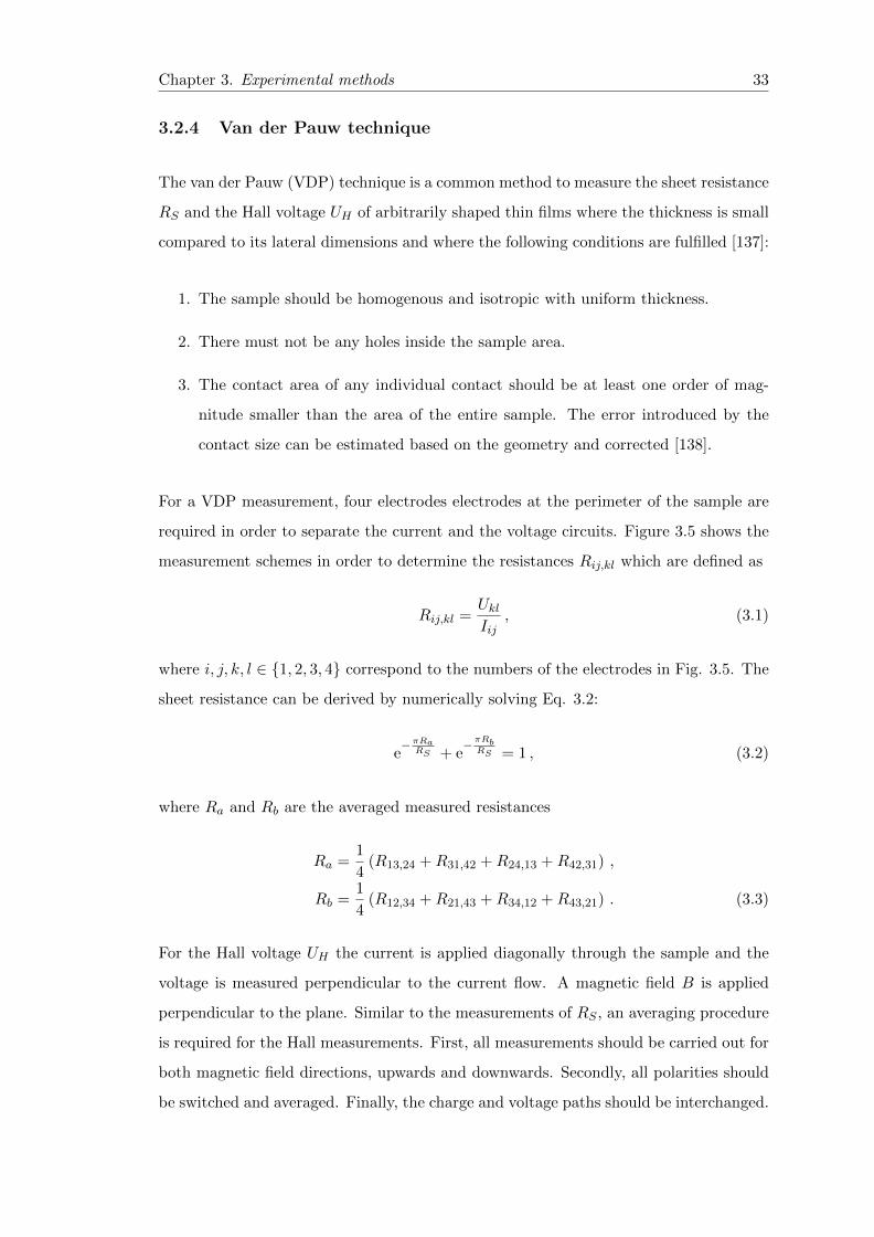
Chapter 3. Experimental methods 33
3.2.4 Van der Pauw technique
The van der Pauw (VDP) technique is a common method to measure the sheet resistance
RS and the Hall voltage UH of arbitrarily shaped thin films where the thickness is small
compared to its lateral dimensions and where the following conditions are fulfilled [137]:
1. The sample should be homogenous and isotropic with uniform thickness.
2. There must not be any holes inside the sample area.
3. The contact area of any individual contact should be at least one order of mag-
nitude smaller than the area of the entire sample. The error introduced by the
contact size can be estimated based on the geometry and corrected [138].
For a VDP measurement, four electrodes electrodes at the perimeter of the sample are
required in order to separate the current and the voltage circuits. Figure 3.5 shows the
measurement schemes in order to determine the resistances Rij,kl which are defined as
Rij,kl =UklIij
, (3.1)
where i, j, k, l ∈ 1, 2, 3, 4 correspond to the numbers of the electrodes in Fig. 3.5. The
sheet resistance can be derived by numerically solving Eq. 3.2:
e−πRaRS + e
−πRbRS = 1 , (3.2)
where Ra and Rb are the averaged measured resistances
Ra =1
4(R13,24 +R31,42 +R24,13 +R42,31) ,
Rb =1
4(R12,34 +R21,43 +R34,12 +R43,21) . (3.3)
For the Hall voltage UH the current is applied diagonally through the sample and the
voltage is measured perpendicular to the current flow. A magnetic field B is applied
perpendicular to the plane. Similar to the measurements of RS , an averaging procedure
is required for the Hall measurements. First, all measurements should be carried out for
both magnetic field directions, upwards and downwards. Secondly, all polarities should
be switched and averaged. Finally, the charge and voltage paths should be interchanged.
Chapter 3. Experimental methods 34
B
1 2
3 4
I+ V+
I− V−
I+ I−
V+ V−
I+ V−
V+ I−
V+ I+
I− V−
R13,24 R12,34
U14,32H U23,14
H
Figure 3.5: Sketch of VDP measurement geometries. An example for each config-uration to determine RS and UH is shown. In order to reach maximum accuracy inthe measurement, it is necessary to switch polarities for the current and voltage or tointerchange current and voltage leads as described in the main text. Hall measurementsrequire an additional magnetic field B perpendicular to the plane.
The overall Hall voltage is then determined by
UH =1
4
(U14,32H + U41,23
H + U23,14H + U32,41
H
), (3.4)
with the four Hall voltages
U14,32H =
1
2
(U14,32 (+B)− U14,32 (−B)
),
U41,23H =
1
2
(U41,23 (+B)− U41,23 (−B)
),
U23,14H =
1
2
(U23,14 (+B)− U23,14 (−B)
),
U32,41H =
1
2
(U32,41 (+B)− U32,41 (−B)
). (3.5)
Here U ij,klH (±B) denotes the detected voltage between contacts k and l with a constant
current between i and j and at the same magnetic field value B pointing up- (+) and
downwards (−).
Chapter 3. Experimental methods 35
3.3 SQUID magnetometry
The superconducting quantum interference device (SQUID) is able to measure small
changes in a magnetic flux with high precision by making use of quantum interference
effects in Josephson junctions [139, 140]. While so–called dc SQUIDs are based on a
superconducting loop with two Josephson junctions, rf SQUIDs contain only one of
such junctions. A detailed description of the operating principles can be found in Refs.
[140, 141], while we refer only to the main results here. The SQUID loop itself is a
flux–to–voltage transducer where the output voltage is modulated by the magnetic flux
enclosed by the loop with a certain periodicity set by the fundamental magnetic flux
quantum Φ0 ≈ 2.07 T m2. The SQUID loop can be coupled inductively to supercon-
ducting detection coils via a so–called flux transformer. In a second–order gradiometer
configuration of the detection coils, not the total flux density is measured but the spa-
tial derivative, which allows for significant noise reduction and thus for the measurement
of very small signals [141]. Here, the magnetic sample has to be moved mechanically
through the pickup coils and the stray field produced by its magnetic moment couples
inductively to the SQUID loop. Now, a feedback loop can be used to keep the mag-
netic flux in the SQUID constant. In this case, the measurement signal is the feedback
current.
In this work we use a Quantum Design MPMS XL which is able to detect magnetic
moments as small as 10−12 A m2 [142]. This SQUID is calibrated to the stray field of a
point–like magnetic dipole. If the stray field of the sample differs significantly from this
ideal situation, the measurement has to be corrected accounting for the shape of the
sample. Geometrical correction factors have been calculated and can be used for this
purpose [143].
3.4 Electron beam lithography
In electron beam lithography (EBL) [144], the basic idea is to use a focused electron
beam of a scanning electron microscope (SEM) to write the desired structure first into
a radiation sensitive polymer, often called “resist”, and to transfer it then from the
resist directly to the substrate/sample by etching, milling or lift–off. For this thesis, so–
called positive resists have been chosen, where those parts exposed to the electron beam
Chapter 3. Experimental methods 36
undergo a chemical reaction enhancing their soluability compared to the unexposed
parts. In the development step, an appropriate solvent creates then a polymeric mask
on the sample. This mask determines the areas on the sample which are directly covered
with metal in a subsequent metallization step (Sec. 3.5). By dissolving the polymer,
the material on the mask is taken away and the desired structure is left behind on the
sample surface (lift–off). With EBL, lateral feature sizes down to the nanometer range
and virtually any pattern can be obtained. The basic underlying physical processes
in EBL are not repeated here as they can be found in literature [144] and have been
summarized in my diploma thesis [145]. Nevertheless, for each experiment in this thesis,
the fabrication is detailed in the respective section, including the EBL recipes.
3.5 Sputtering
In this work, the method of sputtering has been employed to realize metallic contacts
on the surface of silicon/silicon dioxide (Si/SiO2) substrates. Sputtering is based on
glow discharge in order to evaporate a target material by the bombardment with ions
and atoms [146]. A glow discharge is ignited in an argon gas atmosphere by applying
several hundred volts between the material reservoir (target) and the substrate which is
to be coated with the metal film. As a result, a stable plasma is formed and gas ions are
transported towards the cathode. These gas ions impinge on the target directly or release
a collision cascade with neutral gas atoms which eventually hit the target, too. If the
energy transfer to the target overcomes the enthalpy of sublimation, the bombardment
causes an ejection of atoms. The release of target atoms is omnidirectional and some
will reach the substrate, where a thin film starts to grow. Further details about this
technique can be found in Ref. [146].
Chapter 4
Development of charge transport
test structures for graphene and
graphene nanoribbons
This chapter deals with the technical side of the development of electrical circuits on
a carrier substrate, which allow for charge transport experiments in graphene and es-
pecially in GNRs. In the following, we will refer to any such test circuit as a “device”
and a substrate equipped with devices is called a “chip”. For conventional semicon-
ductors, there are established and reliable standard fabrication routes and in the recent
years such a knowledge base has been built up for the fabrication of devices based on
graphene flakes and films as well. In contrast, the technology of bottom–up synthesized
GNRs is still in an early stage, and there is not yet an established standard protocol for
the GNR device fabrication and therefore, we test several different approaches. First,
we describe in detail the initial growth of the graphene nanoribbons, their transfer to a
substrate and the development of appropriate electrical contacts. Secondly, in Sec. 4.4,
we introduce certain success rates, which we define for different stages of the whole de-
vice production process. Based on these success rates we find a reliable way to fabricate
devices to probe charge transport in GNR networks in a systematic way.
37
Chapter 4. Development of charge transport test structures 38
4.1 Synthesis of carbon materials
We start with a description of the synthesis of the different carbon materials which
have been used. The focus lies on the fabrication of nitrogen doped graphene films by
chemical vapor deposition (CVD) and the bottom–up synthesis of GNRs. Furthermore,
within this work, TG discs have been used for electromigration experiments (see Sec.
4.3.3), while charge transport in TG discs has been extensively studied by us previously
in Refs. [145, 147].
4.1.1 Nitrogen–doped graphene
Doping of graphene is a broadly used term and often used in various contexts, ranging
from electrostatic doping using an external electric fields generated by gate electrodes
[148], to adatomic charge transfer doping [9, 10] and finally to heteroatomic doping by
implanting a second atomic species in the graphene crystal lattice [18, 149–158]. In this
work, we focus exclusively on the latter. Different fabrication methods can be used to
incorporate a dopant into the graphene lattice. Hyperthermal ion implantation is an
example for first growing pristine graphene and integrating the dopants in a second step
[159]. However, ion implantation is a poorly controlled stochastic process, where the
quality of the obtained doped graphene depends critically on the implantation beam
energy and dose. Growing doped graphene in only one step, for example by CVD, is
advantageous due to the reduced number of fabrication steps and the potentially higher
throughput. CVD is an efficient method to produce single layer graphene [160], where a
precursor molecule in gas phase condenses on a catalytic substrate and forms a graphene
crystal. Copper is widely used as a substrate in the CVD synthesis of graphene [161].
While in the early stages of CVD grown graphene, the crystal quality was not competi-
tive with mechanically exfoliated graphene, this process has been optimized nowadays,
enabling charge carrier mobilities of up to 350, 000 cm2V−1s−1 in undoped graphene,
by minimizing lattice defects and optimizing the transfer processes [160]. Furthermore,
heteroatomic dopants can easily be integrated by using additional precursors like NH3 or
pyrrole if nitrogen doping is to be obtained [149]. Following this approach, doping with
nitrogen [18, 149–151], boron [152, 153], sulfur [154–156], phosphorus [157] and silicon
[158] atoms has thus far been demonstrated. Among these different dopants, nitrogen
is often a natural choice due to its comparable size to carbon while it has an additional
Chapter 4. Development of charge transport test structures 39
valence electron leading to n (electron) doping when carbon atoms are replaced by ni-
trogen atoms (so called graphitic defects) [162]. Interestingly, p (hole) doping is possible
as well, if other types of defects are formed, which involve the formation of vacancies in
surrounding hexagon rings or distortions of these rings (e.g. so–called pyrrolic, pyridinic
or nitrilic defects) [162]. Direct visualizations of nitrogen doped graphene grown by
CVD shows that graphitic defects are occuring predominantly [163].
4.1.2 Atomically precise graphene nanoribbons
For the fabrication of GNRs, top–down and bottom–up techniques have been developed
and reported. In a top–down approach, an existing structure is modified to yield a
GNR in the end. Established techniques are liquid phase exfoliation (LPE) [164], EBL
patterning [165], electron beam sculpting [166], and unzipping of CNTs [167, 168]. LPE
and CNT unzipping have their advantages in terms of low cost and high throughput, and
EBL offers the highest degree of flexibility for the resulting structure. However, top–
down methods are generally lacking the deterministic control over the edge structure
and ribbon width at the atomic level [164]. The bottom–up method remedies this
shortcoming as both, edge morphology and GNR width, are accurately tailored by the
design of precursor molecules which serve as building blocks to assemble long ribbons.
In this work, we investigate GNRs resulting from surface–assisted synthesis [79, 169, 170]
as well as GNRs from solution–mediated [171–174] synthesis. Both are processes which
have been developed and established at the Max Planck Institute for Polymer Research
in Mainz.1 In the solution–mediated approach, the polymerization of the precursors into
linear polyphenylenes is followed by oxidative cyclodehydrogenation (“graphitization”).
The polymerization is the key step, which determines the final structures of the GNRs
as well as their length. Cove–type GNRs with high longitudinal extension over 600 nm
can be obtained by AB–type Diels–Alder polymerization [174, 175]. An example of such
a cove–type GNR, which is relevant for this work, is shown in Fig. 4.1 and the fabrica-
tion scheme can be extended to obtain other GNR structures, which are, however, not
investigated in this work. Among them are aGNRs [173, 176], various cove–edge GNRs
[74] and chGNRs [80, 177] have been reported. The solution–mediated approach is par-
ticularly interesting as it offers liquid–phase–processable GNRs on a bulk scale with the
1I thank Dr. A. N. and Dr. Z. C., who have been pioneering the research in this field of chemistry.They are part of the group of Prof. Dr. K. M. and kindly provided the supply with GNRs.
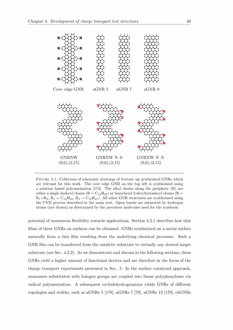
Chapter 4. Development of charge transport test structures 40
NN
N
N
N
N
N
N
S
N
S
N
N
S
N
S
RR
R
R
R
R
R
R
R
R
Cove–edge GNR aGNR 5 aGNR 7 aGNR 9
GNRNW(9,6),(2,15)
GNRNW N–S(9,6),(2,15)
GNRNW N–N(9,6),(2,15)
Figure 4.1: Collection of schematic drawings of bottom–up synthesized GNRs whichare relevant for this work. The cove–edge GNR on the top left is synthesized usinga solution–based polymerization [174]. The alkyl chains along the periphery (R) areeither a single dodecyl chains (R = C12H25) or branchend 2-decyltetradecyl chains (R =R1+R2, R1 = C12H25, R2 = C10H21). All other GNR structures are synthesized usingthe CVD process described in the main text. Open bonds are saturated by hydrogenatoms (not drawn) as determined by the precursor molecules used for the synthesis.
potential of enormeous flexibility towards applications. Section 4.2.1 describes how thin
films of these GNRs on surfaces can be obtained. GNRs synthesized on a metal surface
naturally form a thin film resulting from the underlying chemical processes. Such a
GNR film can be transferred from the catalytic substrate to virtually any desired target
substrate (see Sec. 4.2.2). As we demonstrate and discuss in the following sections, these
GNRs yield a higher amount of functional devices and are therefore in the focus of the
charge transport experiments presented in Sec. 5. In the surface–catalyzed approach,
monomers substituted with halogen groups are coupled into linear polyphenylenes via
radical polymerization. A subsequent cyclodehydrogenation yields GNRs of different
topologies and widths, such as aGNRs 5 [178], aGNRs 7 [79], aGNRs 13 [179], chGNRs
Chapter 4. Development of charge transport test structures 41
[79], zGNRs 6 [180], GNR heterojunctions [169] and even heteroatom–doped GNRs
[181–183]. Initially, this fabrication method has been developed in an ultra–high vac-
uum (UHV) environment, which facilitates the in–situ characterization by scanning
tunneling microscopy. However, if lateral charge transport experiments are the aim, the
elaborate and costly UHV equipment is inconvenient because it restricts the large–scale
fabrication and further use of the GNRs. Therefore, in chapter 5, we make use of GNRs
which have been fabricated in a CVD process developed by Chen et al. allowing for
the inexpensive and high–throughput bottom-up synthesis of structurally well–defined
GNRs. Using this system, the fabrication of chGNRs, doped GNRs (N–doping and N,
S–co–doping) and aGNRs 7 over large areas even under ambient-pressure conditions
has been achieved [82]. Notably, the CVD–grown GNRs exhibit structural quality and
properties comparable with those synthesized under UHV conditions as shown by var-
ious characterization methods as for example Raman spectroscopy. The CVD method
can furthermore yield aGNRs of different widths by using different precursor monomers
[184, 185]. Hence, with the capability of tailoring the monomer building blocks by
modern synthetic chemistry [186], the bottom-up approach yields access to atomically
perfect GNRs with engineered chemical and electronic structures which are currently out
of reach for the top–down approach. Figure 4.1 shows an overview of all CVD–grown
GNRs which have been investigated within this work.
4.1.3 Turbostratic graphene discs
Turbostratic graphene (TG) is a multilayer system of graphene where adjacent layers are
rotated by a certain angle. While already in Bernal–stacked bilayer graphene the energy
dispersion becomes quadratic around its K points [29], such a rotational stacking leads to
a restoration of the linear band structure within a certain energy window [187]. Thus, in
contrast to graphite, TG retains two–dimensional charge–transport properties with high
charge carrier mobilities on the order of 104 cm2 V−1 s−1 and the multilayer structure of
TG discs renders them more resilient than single layer graphene against environmental
influences [147] such as adatoms or charged impurities on the substrate [188]. The
TG discs which have been used for the electromigration experiments described in Sec.
4.3.3 were commercially bought from nTec AS, Oslo2. Their fabrication is based on the
decomposition of hydrocarbons by exposing them to the heat of an inert gas plasma,
2http://www.n-tec.no/
Chapter 4. Development of charge transport test structures 42
which can be carried out on an industrial scale in a plasma-arc reactor. The resulting
carbon material consists of fullerenes, CNTs, open conical carbon structures (also called
micro-cones) and TG micro-discs, which are predominantly flat [189]. The TG discs can
be separated from this mixture of materials by means of sonication, centrifugation and
filtration and subsequently transferred to a substrate as described in Ref. [147].3
4.2 Transfer technniques
For the integration of GNRs into electronic circuits it is necessary to transfer them to a
target substrate. A homogeneous distribution of flat–lying, straight GNRs is desirable
for a reliably high yield of functional devices. In the following sections (Secs. 4.2.1 and
4.2.2), we describe the development of techniques to obtain such thin GNR films for
both types, liquid–phase processable GNRs and CVD–grown GNRs.
4.2.1 Transfer of solution processable GNRs
The main advantage of liquid–phase processable GNRs is that their handling is compar-
atively easy. Dispersed in a liquid, their storage and transport is simple and in principle
they can be readily integrated in device fabrication processes. However, certain pre-
conditions must be fulfilled, i.e. that they show sufficient dispersibility to form stable
dispersions on the one hand, and on the other hand that they form homogenous films
when brought to a surface. In my diploma thesis (Ref. [145]) it has been shown that
cove–edge GNRs dispersed in tetrahydrofuran (THF) form a self–arranged, homogeneous
and flat film on the surface of highly oriented pyrolytic graphite (HOPG) (see Fig. 4.2
(a)). The film was readily obtained by drop casting a volume of a few microliters on the
HOPG sample and letting the solvent evaporate at ambient conditions. Using atomic
force microscopy (AFM) [190], the film can be visualized and the regular arrangement
of GNRs is clearly demonstrated (see Fig. 4.2). However, the same approach does not
yield any comparable result on a SiO2 surface. Here, the GNRs coagulate instead and
form large clusters with no internal order (Fig. 4.2 (b)). For example, resulting from
the hydrophobic carbon surface, bundling and aggregation is known in the case of CNTs
3I thank Dr. Y. H. who provided purified powders of TG discs during my whole project and wheneverthey were needed. She also showed me how to deposit these discs on the surface of a substrate by usinga sticky tape–stamp transfer method.
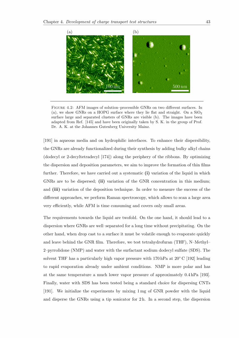
Chapter 4. Development of charge transport test structures 43
(a) (b)
100 nm 500 nm
Figure 4.2: AFM images of solution–processible GNRs on two different surfaces. In(a), we show GNRs on a HOPG surface where they lie flat and straight. On a SiO2
surface large and separated clusters of GNRs are visible (b). The images have beenadapted from Ref. [145] and have been originally taken by S. K. in the group of Prof.Dr. A. K. at the Johannes Gutenberg University Mainz.
[191] in aqueous media and on hydrophilic interfaces. To enhance their dispersibility,
the GNRs are already functionalized during their synthesis by adding bulky alkyl chains
(dodecyl or 2-decyltetradecyl [174]) along the periphery of the ribbons. By optimizing
the dispersion and deposition parameters, we aim to improve the formation of thin films
further. Therefore, we have carried out a systematic (i) variation of the liquid in which
GNRs are to be dispersed; (ii) variation of the GNR concentration in this medium;
and (iii) variation of the deposition technique. In order to measure the success of the
different approaches, we perform Raman spectroscopy, which allows to scan a large area
very efficiently, while AFM is time consuming and covers only small areas.
The requirements towards the liquid are twofold. On the one hand, it should lead to a
dispersion where GNRs are well–separated for a long time without precipitating. On the
other hand, when drop cast to a surface it must be volatile enough to evaporate quickly
and leave behind the GNR film. Therefore, we test tetrahydrofuran (THF), N–Methyl–
2–pyrrolidone (NMP) and water with the surfactant sodium dodecyl sulfate (SDS). The
solvent THF has a particularly high vapor pressure with 170 hPa at 20C [192] leading
to rapid evaporation already under ambient conditions. NMP is more polar and has
at the same temperature a much lower vapor pressure of approximately 0.4 hPa [193].
Finally, water with SDS has been tested being a standard choice for dispersing CNTs
[191]. We initialize the experiments by mixing 1 mg of GNR powder with the liquid
and disperse the GNRs using a tip sonicator for 2 h. In a second step, the dispersion
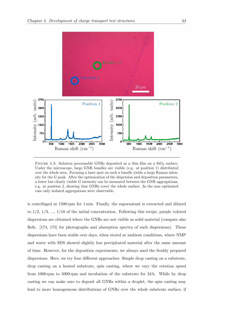
Chapter 4. Development of charge transport test structures 44
Raman shift (cm−1) Raman shift (cm−1)
Inte
nsi
ty(a
rb.
unit
s)
Inte
nsi
ty(a
rb.
unit
s)
25µm
Postition 1
Position 2
Position 1 Position 2
Figure 4.3: Solution–processable GNRs deposited as a thin film on a SiO2 surface.Under the microscope, large GNR bundles are visible (e.g. at position 1) distributedover the whole area. Focusing a laser spot on such a bundle yields a large Raman inten-sity for the G peak. After the optimization of the dispersion and deposition parameters,a lower but clearly visible G intensity can be measured between the GNR aggregations,e.g. at position 2, showing that GNRs cover the whole surface. In the non–optimizedcase only isolated aggregations were observable.
is centrifuged at 1500 rpm for 1 min. Finally, the supernatant is extracted and diluted
to 1/2, 1/3, ..., 1/10 of the initial concentration. Following this recipe, purple–colored
dispersions are obtained where the GNRs are not visible as solid material (compare also
Refs. [174, 175] for photographs and absorption spectra of such dispersions). These
dispersions have been stable over days, when stored at ambient conditions, where NMP
and water with SDS showed slightly less precipitated material after the same amount
of time. However, for the deposition experiments, we always used the freshly prepared
dispersions. Here, we try four different approaches: Simple drop casting on a substrate,
drop casting on a heated substrate, spin casting, where we vary the rotation speed
from 1000 rpm to 5000 rpm and incubation of the substrate for 24 h. While by drop
casting we can make sure to deposit all GNRs within a droplet, the spin casting may
lead to more homogeneous distributions of GNRs over the whole substrate surface, if
Chapter 4. Development of charge transport test structures 45
the adhesion of GNRs is strong enough. Indeed, we obtain the best result for GNRs
dispersed in THF at the lowest concentration (1/10), drop cast on a substrate at a
temperature of 120C. In Fig. 4.3, we show that in this case, we obtain a strong Raman
signal all over the substrate surface and especially at locations, where there are no GNR
aggregates visible under the microscope. Based on our observations, we conclude, that
the GNRs are coagulating too rapidly to form films of the same quality on SiO2 as on
HOPG. Especially when the relative concentration is increasing during the evaporation
process of the solvent, the bundling of GNRs into aggregates is facilitated. Heating the
substrate introduces thermal energy which can keep individual GNRs apart and reduces
the possible interaction time for GNRs to aggregate as the solvent evaporates faster.
Either further functionalization of the GNRs themselves or of the substrate surface will
be necessary to obtain a higher level of internal order in the GNR film.
Hence, despite the remarkable progress of the solution–mediated synthesis, processing of
the resulting GNRs is still a major difficulty due to their limited solubility and tendency
to aggregate in dispersions which also compromises the performance of the electronic
devices based on them. As a result, only very limited modulation of the electrical
resistance with a gate voltage has been observed in our own measurements (compare
[145]) and in other experiments, reported in literature [194–196].
4.2.2 Transfer of GNRs from surfaces
The surface–assisted growth of GNRs by CVD presented in Sec. 4.1.2 as well as the
CVD fabrication of single layer graphene described in Sec. 4.1.1 require a metallic
substrate which catalyzes the reaction. Such metallic surfaces are not suitable for charge
transport experiments due to their high conductivity which would shunt any attempted
lateral charge transport through the graphene immediately. Thus, certain techniques
have been developed to transfer GNR [82, 197] and graphene [160, 198–202] films to
arbitrary substrates. The transfer can be conducted with or without a sacrificial polymer
layer such as poly(methyl methacrylate) (PMMA). A PMMA layer provides additional
mechanical stability and facilitates the transfer of intact films over a large area (see
Fig. A.1 (Appendix A) and Ref. [82]). Without PMMA, however, contamination by
non–dissolvable residues on the GNR film can be avoided, which can make electrically
contacting graphene–based materials difficult [203]. In Fig. 4.4 we depict the transfer
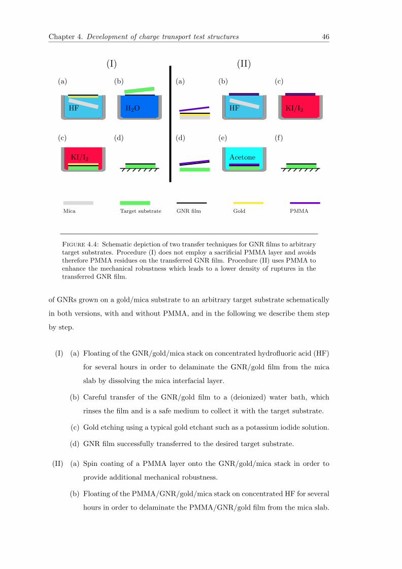
Chapter 4. Development of charge transport test structures 46
(I) (II)
Mica Target substrate GNR film Gold PMMA
HF H2O
KI/I2
HF KI/I2
Acetone
(a) (b)
(c) (d)
(a) (b) (c)
(d) (e) (f)
Figure 4.4: Schematic depiction of two transfer techniques for GNR films to arbitrarytarget substrates. Procedure (I) does not employ a sacrificial PMMA layer and avoidstherefore PMMA residues on the transferred GNR film. Procedure (II) uses PMMA toenhance the mechanical robustness which leads to a lower density of ruptures in thetransferred GNR film.
of GNRs grown on a gold/mica substrate to an arbitrary target substrate schematically
in both versions, with and without PMMA, and in the following we describe them step
by step.
(I) (a) Floating of the GNR/gold/mica stack on concentrated hydrofluoric acid (HF)
for several hours in order to delaminate the GNR/gold film from the mica
slab by dissolving the mica interfacial layer.
(b) Careful transfer of the GNR/gold film to a (deionized) water bath, which
rinses the film and is a safe medium to collect it with the target substrate.
(c) Gold etching using a typical gold etchant such as a potassium iodide solution.
(d) GNR film successfully transferred to the desired target substrate.
(II) (a) Spin coating of a PMMA layer onto the GNR/gold/mica stack in order to
provide additional mechanical robustness.
(b) Floating of the PMMA/GNR/gold/mica stack on concentrated HF for several
hours in order to delaminate the PMMA/GNR/gold film from the mica slab.
Chapter 4. Development of charge transport test structures 47
(c) Gold etching using a typical gold etchant such as a potassium iodide solution.
(d) Transfer of the PMMA/GNR film to the target substrate. This step can take
place either in a water bath, like in (I) or in a dry environment.
(e) Careful transfer of the PMMA/GNR/target substrate stack to an acetone
bath, which dissolves the PMMA layer. After the removal of the PMMA a
rinsing step using isopropanol can be introduced before one lets the GNR film
dry (not shown).
(f) GNR film successfully transferred to the desired target substrate.
Our standard transfer of single layer (doped) graphene films grown by CVD on copper
substrates is very similar to procedure (II) for the GNRs. The copper as catalytic metal
can have a thickness in the range of 101–102 µm and consequently it is stiff enough to be
handled freestanding without the need for mica as a carrying substrate. Consequently,
step (II.b) is not required. The only difference is then to use the appropriate etchant
for the copper, such as iron nitrite or ammonium persulfate. Because of the described
analogies, we do not detail the transfer of single layer graphene here and refer the reader
to the literature, where the process is well documented (e.g. Refs. [198, 199] which
describe exactly the transfer method employed by M. R. for the fabrication of samples
in Sec. 6).
4.3 Device engineering for charge transport in bottom–up
GNRs
In the following section, we detail the development of short channel electrodes and long
channel electrodes and furthermore describe the general schemes of the GNR device
fabrication. The classifications “long” and “short” refer to the separation L of the
electrodes, which is larger than the average length of a GNR in the long channel case.
The lengths of solution–processable GNRs range between 100 and 600 nm [174] while in
the CVD case the average length is about 30 nm [184]. These electrodes are designed to
probe charge transport in GNR networks, while short channel devices ultimately aim to
inject current into single GNRs. In both cases, we inject and measure electrical current
in a two–point configuration between a source and a drain electrode, through the GNRs
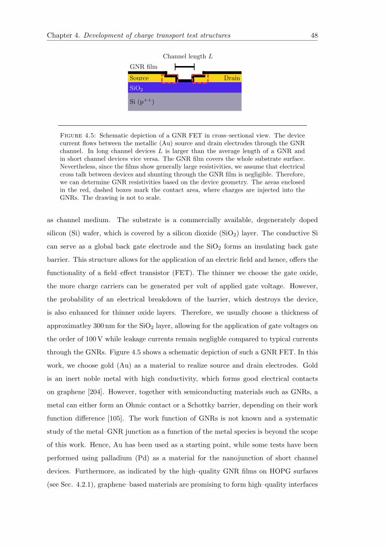
Chapter 4. Development of charge transport test structures 48
GNR film
Source Drain
Channel length L
SiO2
Si (p++)
Figure 4.5: Schematic depiction of a GNR FET in cross–sectional view. The devicecurrent flows between the metallic (Au) source and drain electrodes through the GNRchannel. In long channel devices L is larger than the average length of a GNR andin short channel devices vice versa. The GNR film covers the whole substrate surface.Nevertheless, since the films show generally large resistivities, we assume that electricalcross talk between devices and shunting through the GNR film is negligible. Therefore,we can determine GNR resistivities based on the device geometry. The areas enclosedin the red, dashed boxes mark the contact area, where charges are injected into theGNRs. The drawing is not to scale.
as channel medium. The substrate is a commercially available, degenerately doped
silicon (Si) wafer, which is covered by a silicon dioxide (SiO2) layer. The conductive Si
can serve as a global back gate electrode and the SiO2 forms an insulating back gate
barrier. This structure allows for the application of an electric field and hence, offers the
functionality of a field–effect transistor (FET). The thinner we choose the gate oxide,
the more charge carriers can be generated per volt of applied gate voltage. However,
the probability of an electrical breakdown of the barrier, which destroys the device,
is also enhanced for thinner oxide layers. Therefore, we usually choose a thickness of
approximatley 300 nm for the SiO2 layer, allowing for the application of gate voltages on
the order of 100 V while leakage currents remain negligble compared to typical currents
through the GNRs. Figure 4.5 shows a schematic depiction of such a GNR FET. In this
work, we choose gold (Au) as a material to realize source and drain electrodes. Gold
is an inert noble metal with high conductivity, which forms good electrical contacts
on graphene [204]. However, together with semiconducting materials such as GNRs, a
metal can either form an Ohmic contact or a Schottky barrier, depending on their work
function difference [105]. The work function of GNRs is not known and a systematic
study of the metal–GNR junction as a function of the metal species is beyond the scope
of this work. Hence, Au has been used as a starting point, while some tests have been
performed using palladium (Pd) as a material for the nanojunction of short channel
devices. Furthermore, as indicated by the high–quality GNR films on HOPG surfaces
(see Sec. 4.2.1), graphene–based materials are promising to form high–quality interfaces
Chapter 4. Development of charge transport test structures 49
for Ohmic contacts. This motivates the electromigration study in Sec. 4.3.3 in TG discs,
to form source–drain nanojunctions.
4.3.1 Short channel devices by lithography
Short channel devices are suitable to contact nanoscopic structures like individual GNRs
or magnetic molecules. Consequently, a gap between source and drain must not be larger
than a few nanometers for molecules to fit in, or tens of nanometers for the larger systems
such as GNRs. We explore two possible fabrication approaches for such a nanojunction.
Direct patterning by EBL and the formation of a nanogap by electromigration. We start
with the description of the lithographically defined nanojunctions. Figure 4.6 is a flow
chart of the process, which comprises the following steps:
1. Initial cleaning
• Wafer pieces with a size of approximately 1×1 cm2 are cleaned by immersing
into acetone, isopropanol and distilled water for 1 min each. Afterwards, the
substrates are blow dried by a nitrogen gun and further residual water is
removed from the surface by annealing for 5 min on a hot plate at 130C.
2. First EBL step
• Spin coating of the copolymer methyl methacrylate and methacrylic acid in
ethyl lactate (MMA(8.5)MAA EL6) onto the substrate using a prespin of
500 rpm for 2 s (acceleration 500 rps2) and a mainspin of 3000 rpm for 60 s
(acceleration 3000 rps2). A baking step follows on the hot plate for 90 s at
180C.
• Spin coating of the resist PMMA 950K A4 onto the substrate using a prespin
of 500 rpm for 1 s (acceleration 500 rps2) and a mainspin of 3000 rpm for 60 s
(acceleration 3000 rps2). Baking on the hot plate for 90 s at 180C.
• Electron beam exposure with a dose of 170µC/cm2 at an acceleration voltage
of 10 kV and a beam current of approximately 2.9 nA. For large structures,
such as contact pads and alignment markers, a coarse step size, e.g. 30 nm,
is sufficient.
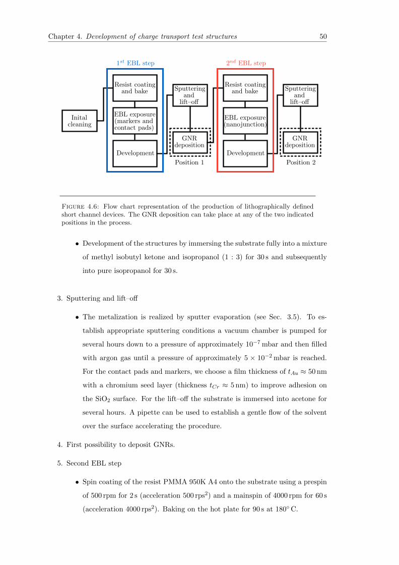
Chapter 4. Development of charge transport test structures 50
Initalcleaning
Resist coatingand bake
EBL exposure(markers andcontact pads)
Development
Sputteringand
lift–off
GNRdeposition
Resist coatingand bake
EBL exposure(nanojunction)
Development
Sputteringand
lift–off
GNRdeposition
1st EBL step 2nd EBL step
Position 1 Position 2
Figure 4.6: Flow chart representation of the production of lithographically definedshort channel devices. The GNR deposition can take place at any of the two indicatedpositions in the process.
• Development of the structures by immersing the substrate fully into a mixture
of methyl isobutyl ketone and isopropanol (1 : 3) for 30 s and subsequently
into pure isopropanol for 30 s.
3. Sputtering and lift–off
• The metalization is realized by sputter evaporation (see Sec. 3.5). To es-
tablish appropriate sputtering conditions a vacuum chamber is pumped for
several hours down to a pressure of approximately 10−7 mbar and then filled
with argon gas until a pressure of approximately 5 × 10⁻² mbar is reached.
For the contact pads and markers, we choose a film thickness of tAu ≈ 50 nm
with a chromium seed layer (thickness tCr ≈ 5 nm) to improve adhesion on
the SiO2 surface. For the lift–off the substrate is immersed into acetone for
several hours. A pipette can be used to establish a gentle flow of the solvent
over the surface accelerating the procedure.
4. First possibility to deposit GNRs.
5. Second EBL step
• Spin coating of the resist PMMA 950K A4 onto the substrate using a prespin
of 500 rpm for 2 s (acceleration 500 rps2) and a mainspin of 4000 rpm for 60 s
(acceleration 4000 rps2). Baking on the hot plate for 90 s at 180C.
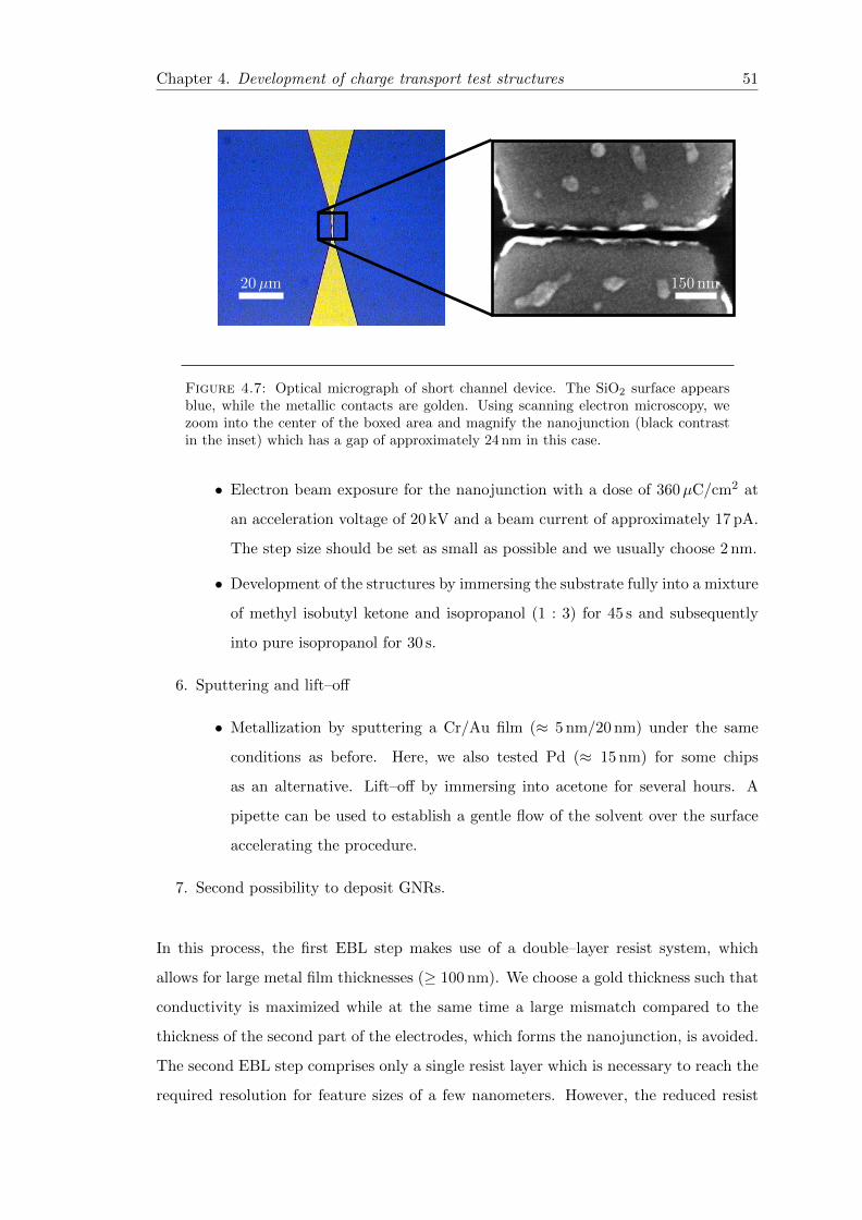
Chapter 4. Development of charge transport test structures 51
20µm 150 nm
Figure 4.7: Optical micrograph of short channel device. The SiO2 surface appearsblue, while the metallic contacts are golden. Using scanning electron microscopy, wezoom into the center of the boxed area and magnify the nanojunction (black contrastin the inset) which has a gap of approximately 24 nm in this case.
• Electron beam exposure for the nanojunction with a dose of 360µC/cm2 at
an acceleration voltage of 20 kV and a beam current of approximately 17 pA.
The step size should be set as small as possible and we usually choose 2 nm.
• Development of the structures by immersing the substrate fully into a mixture
of methyl isobutyl ketone and isopropanol (1 : 3) for 45 s and subsequently
into pure isopropanol for 30 s.
6. Sputtering and lift–off
• Metallization by sputtering a Cr/Au film (≈ 5 nm/20 nm) under the same
conditions as before. Here, we also tested Pd (≈ 15 nm) for some chips
as an alternative. Lift–off by immersing into acetone for several hours. A
pipette can be used to establish a gentle flow of the solvent over the surface
accelerating the procedure.
7. Second possibility to deposit GNRs.
In this process, the first EBL step makes use of a double–layer resist system, which
allows for large metal film thicknesses (≥ 100 nm). We choose a gold thickness such that
conductivity is maximized while at the same time a large mismatch compared to the
thickness of the second part of the electrodes, which forms the nanojunction, is avoided.
The second EBL step comprises only a single resist layer which is necessary to reach the
required resolution for feature sizes of a few nanometers. However, the reduced resist
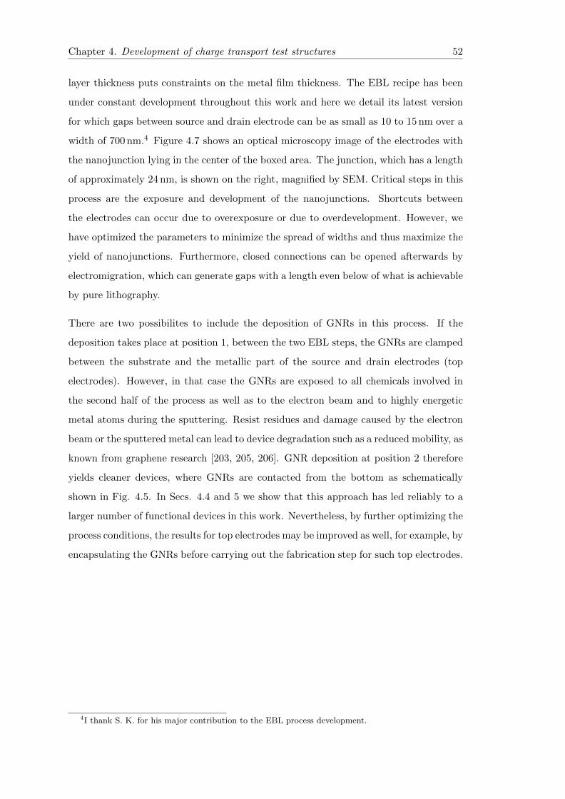
Chapter 4. Development of charge transport test structures 52
layer thickness puts constraints on the metal film thickness. The EBL recipe has been
under constant development throughout this work and here we detail its latest version
for which gaps between source and drain electrode can be as small as 10 to 15 nm over a
width of 700 nm.4 Figure 4.7 shows an optical microscopy image of the electrodes with
the nanojunction lying in the center of the boxed area. The junction, which has a length
of approximately 24 nm, is shown on the right, magnified by SEM. Critical steps in this
process are the exposure and development of the nanojunctions. Shortcuts between
the electrodes can occur due to overexposure or due to overdevelopment. However, we
have optimized the parameters to minimize the spread of widths and thus maximize the
yield of nanojunctions. Furthermore, closed connections can be opened afterwards by
electromigration, which can generate gaps with a length even below of what is achievable
by pure lithography.
There are two possibilites to include the deposition of GNRs in this process. If the
deposition takes place at position 1, between the two EBL steps, the GNRs are clamped
between the substrate and the metallic part of the source and drain electrodes (top
electrodes). However, in that case the GNRs are exposed to all chemicals involved in
the second half of the process as well as to the electron beam and to highly energetic
metal atoms during the sputtering. Resist residues and damage caused by the electron
beam or the sputtered metal can lead to device degradation such as a reduced mobility, as
known from graphene research [203, 205, 206]. GNR deposition at position 2 therefore
yields cleaner devices, where GNRs are contacted from the bottom as schematically
shown in Fig. 4.5. In Secs. 4.4 and 5 we show that this approach has led reliably to a
larger number of functional devices in this work. Nevertheless, by further optimizing the
process conditions, the results for top electrodes may be improved as well, for example, by
encapsulating the GNRs before carrying out the fabrication step for such top electrodes.
4I thank S. K. for his major contribution to the EBL process development.
Chapter 4. Development of charge transport test structures 53
4.3.2 Short channel devices by electromigration in gold
The technique of electromigration (EM) offers an alternative approach to obtain nano-
junctions suitable to act as source–drain electrodes for charge transport experiments
using GNRs. In EM, atoms are moving due to high electrical current densities and
the method has been used to study transport properties of atomic point contacts in
non–magnetic [207, 208] and in magnetic materials [209–211]. Furthermore, it found
application in molecular electronics [212–214] and molecular spintronics [215–217]. For
the displacement of an ion from its position in a conductor, the ion must be subjected
to a force, which is larger than the restoring force given by the chemical binding. This
force arises due to the electric field inside the material E and is given by F = Z∗ eE,
where Z∗ is the effective charge number of an ion in EM [218]. The displacement force
consists of the direct action of the applied electric field and the momentum exchange
between charge carriers (electrons) and the ion. Joule heating further promotes the
displacement. Due to screening, the contribution of momentum exchange is typically
much larger than the direct contribution in metals. Consequently the displacement is
directed on average along the electron flow.
The experimental setup for EM, which has been used in this work, was built by Dr. R.
R. and consists of a Keithley 2400 sourcemeter controlled by a National Instruments
LabVIEW computer programme originally written in the group of Dr. R. H.–V. at the
Karlsruhe Institute for Technology. Starting from a certain initial level V0, the voltage
is incrementally increased up to a target voltage VT being applied to the device which
is to be electromigrated. At this point, the software reduces the voltage automatically
back to V0. Such a loop is called “electromigration cycle”. In order to avoid uncontrolled
breaking of the device, certain protection limits have to be set. The break–off point, GBO
stops the process immediately, when a critical resistance is reached and furthermore, if
the change of resistance is too large, the applied voltage is reduced, depending on a
chosen power decrease parameter. A more detailed description of the working principle
can be found in Ref. [219]. In Ref. [145] we describe the electromigration of gold
electrodes for the purpose of GNR device fabrication. In Fig. 4.8 an example of an
electromigrated nanojunction is shown. The process is more time consuming and less
reliable than defining nanojunctions by lithography (see Sec. 4.3.1). However, smaller
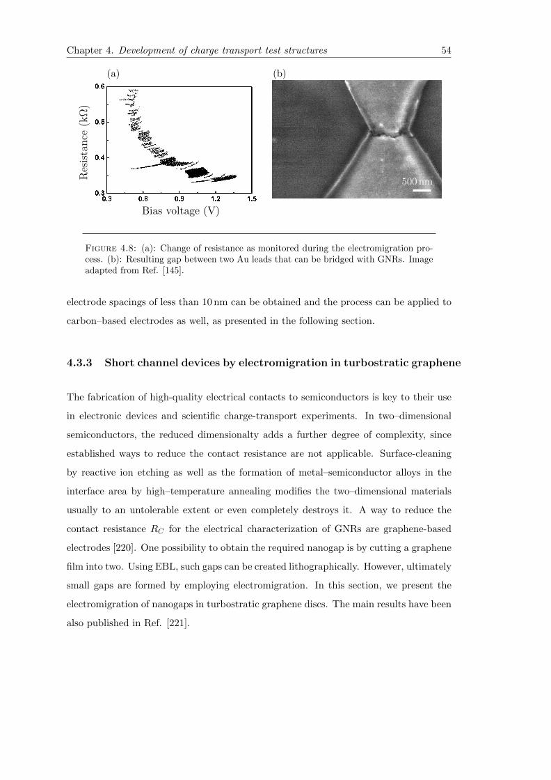
Chapter 4. Development of charge transport test structures 54
(a) (b)
500 nmRes
ista
nce
(kΩ
)
Bias voltage (V)
Figure 4.8: (a): Change of resistance as monitored during the electromigration pro-cess. (b): Resulting gap between two Au leads that can be bridged with GNRs. Imageadapted from Ref. [145].
electrode spacings of less than 10 nm can be obtained and the process can be applied to
carbon–based electrodes as well, as presented in the following section.
4.3.3 Short channel devices by electromigration in turbostratic graphene
The fabrication of high-quality electrical contacts to semiconductors is key to their use
in electronic devices and scientific charge-transport experiments. In two–dimensional
semiconductors, the reduced dimensionalty adds a further degree of complexity, since
established ways to reduce the contact resistance are not applicable. Surface-cleaning
by reactive ion etching as well as the formation of metal–semiconductor alloys in the
interface area by high–temperature annealing modifies the two–dimensional materials
usually to an untolerable extent or even completely destroys it. A way to reduce the
contact resistance RC for the electrical characterization of GNRs are graphene-based
electrodes [220]. One possibility to obtain the required nanogap is by cutting a graphene
film into two. Using EBL, such gaps can be created lithographically. However, ultimately
small gaps are formed by employing electromigration. In this section, we present the
electromigration of nanogaps in turbostratic graphene discs. The main results have been
also published in Ref. [221].
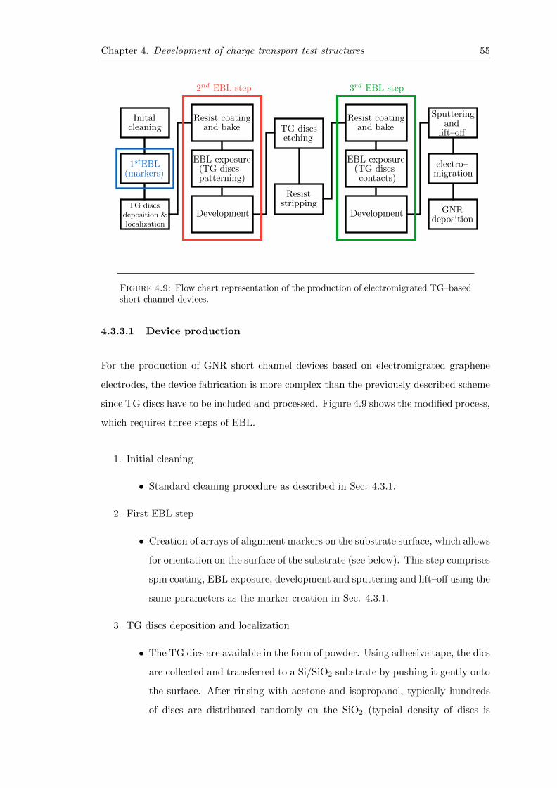
Chapter 4. Development of charge transport test structures 55
Initalcleaning
1stEBL(markers)
TG discs
deposition &localization
Resist coatingand bake
EBL exposure(TG discspatterning)
Development
TG discsetching
Resiststripping
Resist coatingand bake
EBL exposure(TG discscontacts)
Development
Sputteringand
lift–off
electro–migration
GNRdeposition
2nd EBL step 3rd EBL step
Figure 4.9: Flow chart representation of the production of electromigrated TG–basedshort channel devices.
4.3.3.1 Device production
For the production of GNR short channel devices based on electromigrated graphene
electrodes, the device fabrication is more complex than the previously described scheme
since TG discs have to be included and processed. Figure 4.9 shows the modified process,
which requires three steps of EBL.
1. Initial cleaning
• Standard cleaning procedure as described in Sec. 4.3.1.
2. First EBL step
• Creation of arrays of alignment markers on the substrate surface, which allows
for orientation on the surface of the substrate (see below). This step comprises
spin coating, EBL exposure, development and sputtering and lift–off using the
same parameters as the marker creation in Sec. 4.3.1.
3. TG discs deposition and localization
• The TG dics are available in the form of powder. Using adhesive tape, the dics
are collected and transferred to a Si/SiO2 substrate by pushing it gently onto
the surface. After rinsing with acetone and isopropanol, typically hundreds
of discs are distributed randomly on the SiO2 (typcial density of discs is
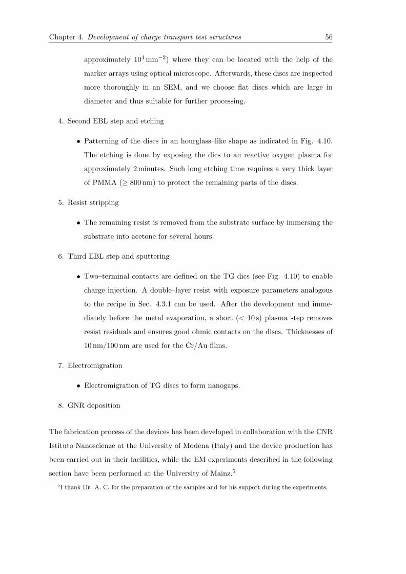
Chapter 4. Development of charge transport test structures 56
approximately 104 mm−2) where they can be located with the help of the
marker arrays using optical microscope. Afterwards, these discs are inspected
more thoroughly in an SEM, and we choose flat discs which are large in
diameter and thus suitable for further processing.
4. Second EBL step and etching
• Patterning of the discs in an hourglass–like shape as indicated in Fig. 4.10.
The etching is done by exposing the dics to an reactive oxygen plasma for
approximately 2 minutes. Such long etching time requires a very thick layer
of PMMA (≥ 800 nm) to protect the remaining parts of the discs.
5. Resist stripping
• The remaining resist is removed from the substrate surface by immersing the
substrate into acetone for several hours.
6. Third EBL step and sputtering
• Two–terminal contacts are defined on the TG dics (see Fig. 4.10) to enable
charge injection. A double–layer resist with exposure parameters analogous
to the recipe in Sec. 4.3.1 can be used. After the development and imme-
diately before the metal evaporation, a short (< 10 s) plasma step removes
resist residuals and ensures good ohmic contacts on the discs. Thicknesses of
10 nm/100 nm are used for the Cr/Au films.
7. Electromigration
• Electromigration of TG discs to form nanogaps.
8. GNR deposition
The fabrication process of the devices has been developed in collaboration with the CNR
Istituto Nanoscienze at the University of Modena (Italy) and the device production has
been carried out in their facilities, while the EM experiments described in the following
section have been performed at the University of Mainz.5
5I thank Dr. A. C. for the preparation of the samples and for his support during the experiments.
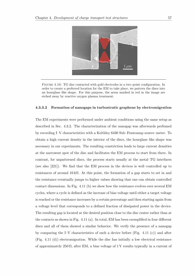
Chapter 4. Development of charge transport test structures 57
1µm
Figure 4.10: TG disc contacted with gold electrodes in a two–point configuration. Inorder to create a preferred location for the EM to take place, we pattern the discs intoan hourglass–like shape. For this purpose, the areas marked in red in the image areetched away by reactive oxygen plasma treatment.
4.3.3.2 Formation of nanogaps in turbostratic graphene by electromigration
The EM experiments were performed under ambient conditions using the same setup as
described in Sec. 4.3.2. The characterization of the nanogap was afterwards perfomed
by recording I–V characteristics with a Keithley 6430 Sub–Femtoamp source–meter. To
obtain a high current density in the interior of the discs, the hourglass–like shape was
necessary in our experiments. The resulting constriction leads to large current densities
at the narrowest spot of the disc and facilitates the EM process to start from there. In
contrast, for unpatterned discs, the process starts usually at the metal–TG interfaces
(see also [221]). We find that the EM process in the devices is well–controlled up to
resistances of around 16 kΩ. At this point, the formation of a gap starts to set in and
the resistance eventually jumps to higher values showing that one can obtain controlled
contact dimensions. In Fig. 4.11 (b) we show how the resistance evolves over several EM
cycles, where a cycle is defined as the increase of bias voltage until either a target voltage
is reached or the resistance increases by a certain percentage and then starting again from
a voltage level that corresponds to a defined fraction of dissipated power in the device.
The resulting gap is located at the desired position close to the disc center rather than at
the contacts as shown in Fig. 4.11 (a). In total, EM has been exemplified in four different
discs and all of them showed a similar behavior. We verify the presence of a nanogap
by comparing the I–V characteristics of such a device before (Fig. 4.11 (c)) and after
(Fig. 4.11 (d)) electromigration. While the disc has initially a low electrical resistance
of approximately 250 Ω, after EM, a bias voltage of 1 V results typically in a current of
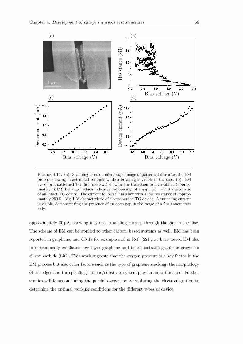
Chapter 4. Development of charge transport test structures 58
(a) (b)
(c) (d)
Bias voltage (V)Bias voltage (V)
Bias voltage (V)
Res
ista
nce
(kΩ
)
Dev
ice
curr
ent
(mA
)
Dev
ice
curr
ent
(pA
)
1µm
Figure 4.11: (a): Scanning electron microscope image of patterned disc after the EMprocess showing intact metal contacts while a breaking is visible in the disc. (b): EMcycle for a patterned TG disc (see text) showing the transition to high–ohmic (approx-imately 16 kΩ) behavior, which indicates the opening of a gap. (c): I–V characteristicof an intact TG device. The current follows Ohm’s law with a low resistance of approx-imately 250 Ω. (d): I–V characteristic of electroburned TG device. A tunneling currentis visible, demonstrating the presence of an open gap in the range of a few nanometersonly.
approximately 80 pA, showing a typical tunneling current through the gap in the disc.
The scheme of EM can be applied to other carbon–based systems as well. EM has been
reported in graphene, and CNTs for example and in Ref. [221], we have tested EM also
in mechanically exfoliated few–layer graphene and in turbostratic graphene grown on
silicon carbide (SiC). This work suggests that the oxygen pressure is a key factor in the
EM process but also other factors such as the type of graphene stacking, the morphology
of the edges and the specific graphene/substrate system play an important role. Further
studies will focus on tuning the partial oxygen pressure during the electromigration to
determine the optimal working conditions for the different types of device.
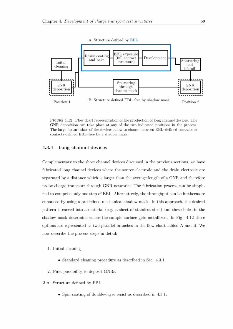
Chapter 4. Development of charge transport test structures 59
Initalcleaning
GNRdeposition
Resist coatingand bake
EBL exposure(full contact
structure)Development
Sputteringthrough
shadow mask
Sputteringand
lift–off
GNRdeposition
Position 1 Position 2
A: Structure defined by EBL
B: Structure defined EBL–free by shadow mask
Figure 4.12: Flow chart representation of the production of long channel devices. TheGNR deposition can take place at any of the two indicated positions in the process.The large feature sizes of the devices allow to choose between EBL–defined contacts orcontacts defined EBL–free by a shadow mask.
4.3.4 Long channel devices
Complementary to the short channel devices discussed in the previous sections, we have
fabricated long channel devices where the source electrode and the drain electrode are
separated by a distance which is larger than the average length of a GNR and therefore
probe charge transport through GNR networks. The fabrication process can be simpli-
fied to comprise only one step of EBL. Alternatively, the throughput can be furthermore
enhanced by using a predefined mechanical shadow mask. In this approach, the desired
pattern is carved into a material (e.g. a sheet of stainless steel) and these holes in the
shadow mask determine where the sample surface gets metallized. In Fig. 4.12 these
options are represented as two parallel branches in the flow chart labled A and B. We
now describe the process steps in detail:
1. Initial cleaning
• Standard cleaning procedure as described in Sec. 4.3.1.
2. First possibility to deposit GNRs.
3.A. Structure defined by EBL
• Spin coating of double–layer resist as described in 4.3.1.
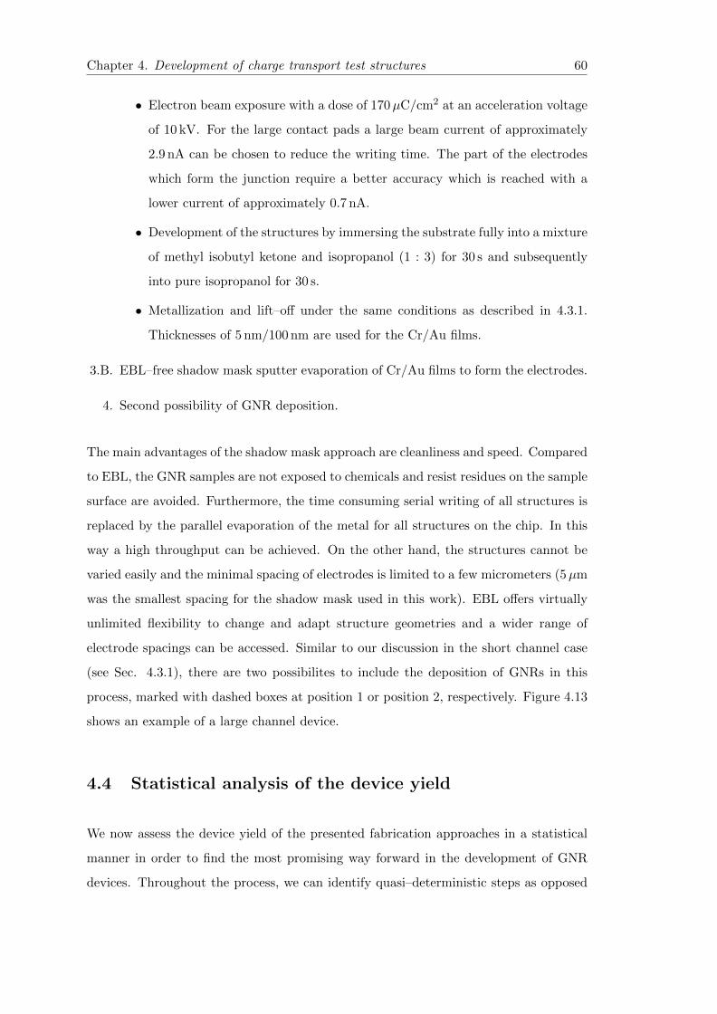
Chapter 4. Development of charge transport test structures 60
• Electron beam exposure with a dose of 170µC/cm2 at an acceleration voltage
of 10 kV. For the large contact pads a large beam current of approximately
2.9 nA can be chosen to reduce the writing time. The part of the electrodes
which form the junction require a better accuracy which is reached with a
lower current of approximately 0.7 nA.
• Development of the structures by immersing the substrate fully into a mixture
of methyl isobutyl ketone and isopropanol (1 : 3) for 30 s and subsequently
into pure isopropanol for 30 s.
• Metallization and lift–off under the same conditions as described in 4.3.1.
Thicknesses of 5 nm/100 nm are used for the Cr/Au films.
3.B. EBL–free shadow mask sputter evaporation of Cr/Au films to form the electrodes.
4. Second possibility of GNR deposition.
The main advantages of the shadow mask approach are cleanliness and speed. Compared
to EBL, the GNR samples are not exposed to chemicals and resist residues on the sample
surface are avoided. Furthermore, the time consuming serial writing of all structures is
replaced by the parallel evaporation of the metal for all structures on the chip. In this
way a high throughput can be achieved. On the other hand, the structures cannot be
varied easily and the minimal spacing of electrodes is limited to a few micrometers (5µm
was the smallest spacing for the shadow mask used in this work). EBL offers virtually
unlimited flexibility to change and adapt structure geometries and a wider range of
electrode spacings can be accessed. Similar to our discussion in the short channel case
(see Sec. 4.3.1), there are two possibilites to include the deposition of GNRs in this
process, marked with dashed boxes at position 1 or position 2, respectively. Figure 4.13
shows an example of a large channel device.
4.4 Statistical analysis of the device yield
We now assess the device yield of the presented fabrication approaches in a statistical
manner in order to find the most promising way forward in the development of GNR
devices. Throughout the process, we can identify quasi–deterministic steps as opposed
Chapter 4. Development of charge transport test structures 61
500µm 20µm
Figure 4.13: Optical micrograph of a large channel device. The SiO2 surface appearsblue, while the metallic contacts are golden. The inset shows a zoom into the center ofthe boxed area magnifying the channel region where charge current flows through GNRnetworks (marked in red). The junction has a separation of approximately 500 nm inthis case.
to steps, which involve a certain stochasticity. As an example, lithography of large struc-
tures is typically a very well–controlled technique and has an excellent reproducibility
of the result. In contrast, the integration of the GNRs adds a stochastic element to
the device fabrication since the synthesis and deposition of GNRs is not controlled on
the level of individual ribbons. Instead, we produce and process always a large number
of GNRs in parallel and their position, orientation and individual structural integrity
are random when they are deposited on the substrate surface, although the synthesis is
perfect on the atomic level dictated by the underlying chemical reaction.
The fabrication of the source and the drain electrodes, which build the backbone for any
GNR device, relies to a large extent on EBL. As already pointed out, there is basically
no randomness in the lithography process as long as the feature sizes are large. Hence, a
yield of up to 100 % satisfactory electrode structures can be obtained for the long chan-
nel devices. The situation changes for the short channel devices. On the scale of a few
nanometers, which is the required separation of the electrode leads of the nanojunction,
the EBL resolution becomes limited by the structure of the resist (e.g. size of polymer-
chains or height corrugations across the film) and the interaction volume when electrons
impinge. Hence, there is a certain spread in the obtained electrode gaps where some can
even be connected. Based on more than 2000 attempted lithographies, we achieved a
success rate of 70 % for devices with a spacing on the order of 15 to 20 nm. Connected
devices, however, can be subjected to EM as described in Sec. 4.3.2. EM is much less
Chapter 4. Development of charge transport test structures 62
controlled than EBL and it is time consuming, where the EM of a single junction can
take hours. Six out of ten tested devices (60 % success rate) yielded nanogaps on the or-
der of a few nanometers, while the remaining four ended in an uncontrolled destruction
of the device. Due to the small number of attempted EMs in TG, the success rate is not
representative and is therefore not further discussed here. More detailed information
about EM in TG and other graphene allotropes are given in Ref. [221].
The integration of GNRs as the channel medium of the FET devices described in the
previous sections is one of the most delicate parts of the whole process. In Secs. 4.2.1 and
4.2.2 we presented the methods for GNR deposition on a surface, where Raman spec-
troscopy is a versatile tool to judge the quality of the resulting GNR films. Especially
using the transfer techniques for CVD–grown GNRs, homogenous films can be obtained
which show uniform Raman signals over an area of more than 100 mm2 (see Fig. A.1
(Appendix A) and Ref. [82]). However, to measure the success of the device integration,
we define two further figures of merit. In a first stage, the conductivity of the device
should increase drastically compared to an open device, where only tunnel currents or
leakage currents through the substrate might flow. If this is not the case, charges are
not efficiently injected into the GNRs and the device is unusable. Secondly, due to the
semiconducting nature of the GNRs, we expect to observe an electric field effect, i.e. the
modulation of a source–drain current using a gate voltage. Finally, even after successful
device patterning and GNR deposition, a device can still be compromised if a leakage
current between gate and drain electrode is too large. For the following discussion of
the yield of solution–processable and CVD–grown GNR devices, we subsume lithogra-
phy failures and gate leakages under a total fabrication failure rate (or success rate,
respectively) and contrast this number to the amount of devices with a measurable (and
gate–tunable) conductivity. The ratio of these two rates indicates whether the device
yield is limited by the former or the latter.
In the case of the solution–processable GNRs, around 1000 short channel devices were
measured, where we transferred cove–edge GNRs onto previously fabricated junctions
(according to the process diagram in Fig. 4.9 or position 2 of the process diagram
in Fig. 4.6). After the application of GNRs, a fraction of approximately 0.5 % of all
devices displayed resistances lower than the open nanojunction, however with a large
spread ranging from Megaohms to Gigaohms and without significant tunability by a
gate voltage. The device yield is clearly limited by the efficiency of charge injection
Chapter 4. Development of charge transport test structures 63
into the GNRs and not by fabrication failures. Secondly, roughly 1000 further short
channel devices with CVD–grown (undoped) GNRNWs have been tested. In this case,
approximately 1 % of all devices showed a measurable current with a similar distribu-
tion of resistances as for the cove–edge GNRs, where, again, the gate dependence was
negligible. The device yield did not depend on the position of the GNR transfer in the
process (transfer before or after defining contacts) and was furthermore also indepen-
dent on Au or Pd as contacting material. Many reports attempting to fabricate FETs
based on a single or only few GNRs discuss the issue of Schottky–like energy barriers at
the metal/GNR interfaces, which inhibit the current flow and are thus one major limi-
tation of charge injection [82, 197, 222]. Such barriers due to band mismatch between
channel and contact metal degrade the transistor performance and lead to limited gate
modulation. A second factor influencing the electric field effect is the ratio of channel
length and gate barrier thickness. For a thick gate barrier oxide of 300 nm the metallic
leads screen a large fraction of the electric field, if the channel length is in the range of
only a few nanometers. In a situation where the device resistance is already limited by
Schottky–barriers, no field effect can be observed. These results have also been detailed
in Ref. [82], where furthermore a comparison is drawn between metallic short channel
devices, metallic long channel devices6 and graphene–based short channel devices7.
Indeed, the situation is drastically different for long channel devices with (CVD–grown)
GNRNWs. The process as depicted in Fig. 4.12 offers four different ways to produce
a device as there are two possible positions for the GNR deposition and two methods
to realize the metallic source–drain electrodes. We have tested two out of these four
combinations. In the first one, the GNR deposition takes place at position 1, where
we use the transfer technique without a supporting PMMA layer. The electrodes are
sputtered through a metallic shadow mask. We choose this combination (1.B) because it
allows to eliminate any contamination due to resist residues from the process. Secondly,
we test a fabrication route where the GNR deposition takes place at position 2 and EBL
is used to define contacts. This combination (2.A) allows only for a GNR transfer with
a supporting PMMA layer, because otherwise the electrodes would be destroyed in the
6For this publication, the measurements on chGNR long channel devices have been carried out bythe collaborating group of Prof. Dr. C. Z. at the University of Southern California, Los Angeles.
7For this publication, the measurements on chGNR graphene–based short channel devices have beencarried out by the collaborating group of Prof. Dr. M. A. at the University of Modena. Since thisgroup focuses on the graphene–based electrodes and our focus lies on devices with metallic electrodes,we do not detail the success statistics for graphene–based devices here. Very detailed information andstatistical analyzes can be found in Refs. [196, 223].
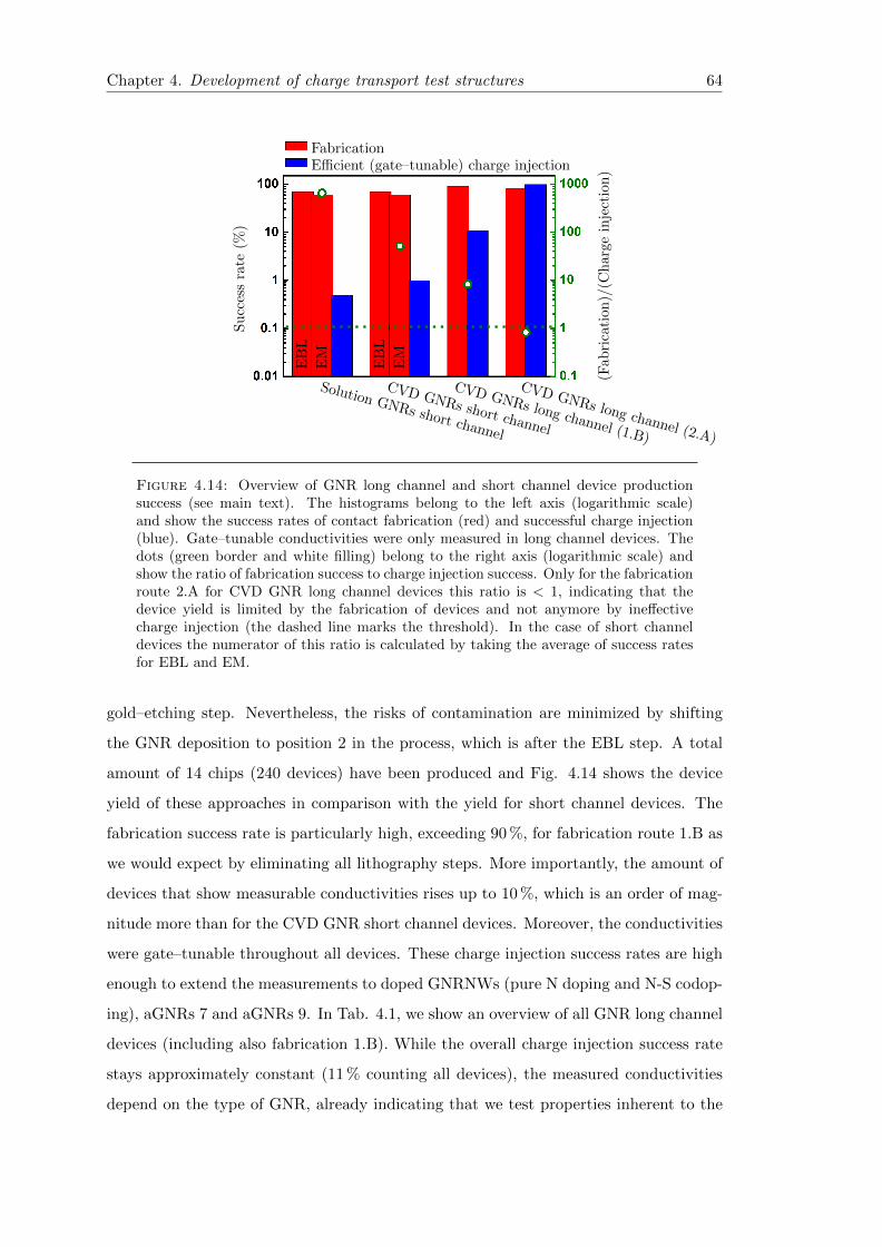
Chapter 4. Development of charge transport test structures 64
FabricationEfficient (gate–tunable) charge injection
Solution GNRs short channel
CVD GNRs short channel
CVD GNRs long channel (1.B)
CVD GNRs long channel (2.A)
EB
L
EM
EB
L
EM
Su
cces
sra
te(%
)
(Fab
rica
tion
)/(C
har
ge
inje
ctio
n)
Figure 4.14: Overview of GNR long channel and short channel device productionsuccess (see main text). The histograms belong to the left axis (logarithmic scale)and show the success rates of contact fabrication (red) and successful charge injection(blue). Gate–tunable conductivities were only measured in long channel devices. Thedots (green border and white filling) belong to the right axis (logarithmic scale) andshow the ratio of fabrication success to charge injection success. Only for the fabricationroute 2.A for CVD GNR long channel devices this ratio is < 1, indicating that thedevice yield is limited by the fabrication of devices and not anymore by ineffectivecharge injection (the dashed line marks the threshold). In the case of short channeldevices the numerator of this ratio is calculated by taking the average of success ratesfor EBL and EM.
gold–etching step. Nevertheless, the risks of contamination are minimized by shifting
the GNR deposition to position 2 in the process, which is after the EBL step. A total
amount of 14 chips (240 devices) have been produced and Fig. 4.14 shows the device
yield of these approaches in comparison with the yield for short channel devices. The
fabrication success rate is particularly high, exceeding 90 %, for fabrication route 1.B as
we would expect by eliminating all lithography steps. More importantly, the amount of
devices that show measurable conductivities rises up to 10 %, which is an order of mag-
nitude more than for the CVD GNR short channel devices. Moreover, the conductivities
were gate–tunable throughout all devices. These charge injection success rates are high
enough to extend the measurements to doped GNRNWs (pure N doping and N-S codop-
ing), aGNRs 7 and aGNRs 9. In Tab. 4.1, we show an overview of all GNR long channel
devices (including also fabrication 1.B). While the overall charge injection success rate
stays approximately constant (11 % counting all devices), the measured conductivities
depend on the type of GNR, already indicating that we test properties inherent to the
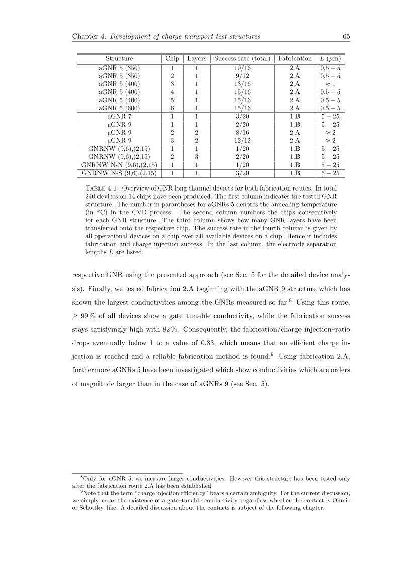
Chapter 4. Development of charge transport test structures 65
Structure Chip Layers Success rate (total) Fabrication L (µm)
aGNR 5 (350) 1 1 10/16 2.A 0.5− 5aGNR 5 (350) 2 1 9/12 2.A 0.5− 5aGNR 5 (400) 3 1 13/16 2.A ≈ 1aGNR 5 (400) 4 1 15/16 2.A 0.5− 5aGNR 5 (400) 5 1 15/16 2.A 0.5− 5aGNR 5 (600) 6 1 15/16 2.A 0.5− 5
aGNR 7 1 1 3/20 1.B 5− 25aGNR 9 1 1 2/20 1.B 5− 25aGNR 9 2 2 8/16 2.A ≈ 2aGNR 9 3 2 12/12 2.A ≈ 2
GNRNW (9,6),(2,15) 1 1 1/20 1.B 5− 25GNRNW (9,6),(2,15) 2 3 2/20 1.B 5− 25
GNRNW N-N (9,6),(2,15) 1 1 1/20 1.B 5− 25GNRNW N-S (9,6),(2,15) 1 1 3/20 1.B 5− 25
Table 4.1: Overview of GNR long channel devices for both fabrication routes. In total240 devices on 14 chips have been produced. The first column indicates the tested GNRstructure. The number in parantheses for aGNRs 5 denotes the annealing temperature(in C) in the CVD process. The second column numbers the chips consecutivelyfor each GNR structure. The third column shows how many GNR layers have beentransferred onto the respective chip. The success rate in the fourth column is given byall operational devices on a chip over all available devices on a chip. Hence it includesfabrication and charge injection success. In the last column, the electrode separationlengths L are listed.
respective GNR using the presented approach (see Sec. 5 for the detailed device analy-
sis). Finally, we tested fabrication 2.A beginning with the aGNR 9 structure which has
shown the largest conductivities among the GNRs measured so far.8 Using this route,
≥ 99 % of all devices show a gate–tunable conductivity, while the fabrication success
stays satisfyingly high with 82 %. Consequently, the fabrication/charge injection–ratio
drops eventually below 1 to a value of 0.83, which means that an efficient charge in-
jection is reached and a reliable fabrication method is found.9 Using fabrication 2.A,
furthermore aGNRs 5 have been investigated which show conductivities which are orders
of magnitude larger than in the case of aGNRs 9 (see Sec. 5).
8Only for aGNR 5, we measure larger conductivities. However this structure has been tested onlyafter the fabrication route 2.A has been established.
9Note that the term “charge injection efficiency” bears a certain ambiguity. For the current discussion,we simply mean the existence of a gate–tunable conductivity, regardless whether the contact is Ohmicor Schottky–like. A detailed discussion about the contacts is subject of the following chapter.
Chapter 4. Development of charge transport test structures 66
4.5 Conclusion and outlook
To achieve the vision of nano– or molecular electronics, which offer novel functionalities,
several technological challenges need to be overcome. In particular the question how
to embed nano–scale objects such as a graphene nanoribbons in electronic circuits in
a reliable way suitable for the mass production of devices needs to be solved. In this
chapter we presented the methods and techniques to synthesize different GNRs and
integrate them in short channel and long channel field effect transistor test structures.10
There are fundamentally two different approaches to obtain atomically perfect GNRs,
which are Diels–Alder polymerization in solution and metal–catalyzed CVD. For their
device integration, the GNRs have to be transferred to a substrate with an insulating
surface (e.g. SiO2). We showed that the formation of thin solution–processable GNR
films is limited by their tendency to agglomerate (even already in a liquid medium).
This leads to coarse grained dispersions and the risk of GNR bundle formation instead
of a homogenous thin film on a SiO2 surface. A satisfying result has been obtained
using a heated target substrate and optimized deposition conditions. A promising path
for the improvement of the GNR dispersibility is side–chain engineering [174]. On the
other hand, the optimization of device integration can be tackled in two ways. Firstly,
graphitic electrodes can be used, where π-π interactions facilitate the alignment of GNRs.
Secondly, the homogeneity of thin films can be improved by functionlization of the GNRs
themselves and of the substrate surface. Together with optimized deposition techniques
of solution–processable GNRs as discussed in Sec. 4.2.1, further advances will become
possible. Besides the discussed techniques, also alternatives to deposit GNRs should
be systematically investigated, as for example the electrospray method [196] which has
not been considered in this work. Furthermore, in the case of CVD–grown GNRs, a
thin film is naturally formed during their synthesis. This film can be transferred to a
target surface which offers a straight–forward way for device integration. By engineering
this process, we have found a reliable way to fabricate long channel FET devices with
a device yield approaching 100 %. This result finally enables the systematic study of
the electronic properties in graphene nanostructures as a function of their width, edge
structure and functionalization (e.g. heteroatomic doping).
10The synthesis was developed in the Max Planck Institute for Polymer Research while the deviceengineering is an integral part of this work.
Chapter 5
Charge transport in networks of
bottom–up graphene nanoribbons
Graphene nanoribbons, synthesized bottom–up by chemical methods, are the ideal test
systems for a variety of theoretical predictions and expectations concerning the electronic
and magnetic properties of such ultra–narrow and atomically perfect carbon structures
[5–7]. Experimental work so far has been largely focussed on spectroscopic techniques
[79, 169, 180], while lateral charge transport remains a challenge. Although first short–
channel device prototypes show promising performance [195, 197, 222], a thorough in-
vestigation of the underlying charge transport mechanism is so far missing. Due to the
difficulties in fabricating single–ribbon devices (Sec. 4, Refs. [197, 222]) many simple
but important experiments are impeded, e.g. testing the channel length dependence
of the charge transport, or the extraction of the Schottky–barrier heights, when large
energy barriers are claimed to be the dominant origin of the observed current–voltage
signatures [197, 222]. With the reliable device fabrication of long channel devices being
established as presented in Sec. 4.3.4, these fundamental tests become possible for the
first time and their results are presented in this chapter. Herein, the role of contacts
is clarified by a transmission line method, where we find Ohmic contacts which do not
limit the charge injection in our devices in contrast to the Schottky–barrier dominated
contacts in previouse studies [197, 222]. As the most important result, we demonstrate
a universal scaling of the channel current over a wide range of bias voltages and temper-
atures, showing that charge hopping is the dominant transport mechanism, which sets
limits to the conductivity and mobility in devices where the channel is comprised of more
67
Chapter 5. Charge transport in GNR networks 68
than one single ribbon. In addition, we find an intriguing positive magnetoresistance in
aGNR 5, which is absent in aGNR 9 and is in contrast to previous experimental work
that shows negative magnetoresistance in top–down fabricated GNRs [224].
5.1 Experimental details
All GNR films discussed in the following have been synthesized following the CVD
method as detailed in Sec. 4.1.2. While the general procedure was identical for the
growth of all films, the choice of the precursor molecule yielded different types of GNRs.
The transfer from the Mica/Au substrate to a wafer of highly doped Si with a tOx =
300 nm thick SiO2 layer was carried out according to Sec. 4.2.2 and after the chip
fabrication was complete, we performed Raman spectroscopy on the films in order to
confirm the structural integrity and rule out any severe alterations of the GNRs due to
the transfer.1 In Fig. 5.1 we present representative Raman spectra taken on films of
aGNR 9 and of aGNR 5 (see Fig. B.1 in Appendix B for Raman spectra of all other
GNR species listed in Tab. 4.1). All measurements were performed with a Bruker RFS
100/S Raman spectrometer using a laser beam with an excitation wavelength of 532 nm.
Comparing these spectra with literature reports [82, 184, 185], we find an excellent agree-
ment for all GNR species confirming that the GNRs are still intact after the transfer.
The width of the GNRs which are composing the films can be identfied with the help
of the RBM in the Raman signature (compare Sec. 3.1). For aGNR 9, we find the
RBM peak at approximately 311 cm−1. In the Raman spectrum of the aGNR 5 film,
we find two RBM lines, one at approximately 533 cm−1 and the other at approximately
283 cm−1. While the former is associated to GNRs with 5 carbon atoms across the rib-
bon, the latter indicates the presence of GNRs that are twice as wide (10 carbon atoms).
We attribute the occurrence of this peak to a small fraction of aGNR 10 contained in the
film, which are produced by a lateral fusion process of two aGNR 5 units. Such fusion
depends on the annealing temperature and at the 400 C only a small number of GNRs
fuse together [185], such that we can neglect their contribution to any charge trans-
port experiment in the following sections. At room temperature, these charge transport
experiments have been performed using the electrical characterization setup in a nitro-
gen glove box described in Sec. 3.2.1, while the variable temperature measurements
1I thank Dr. Z. C. for the growth of the GNR films and for performing Raman spectroscopy on them.
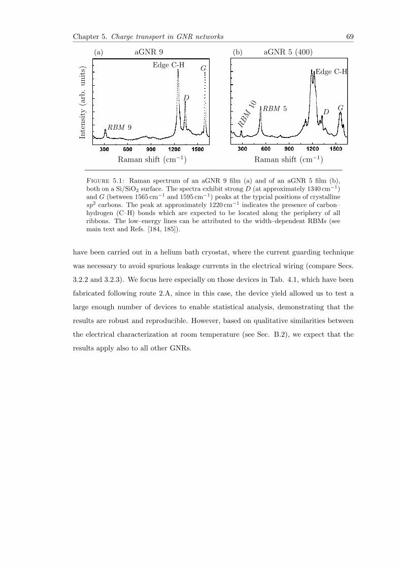
Chapter 5. Charge transport in GNR networks 69
(a) aGNR 9
Raman shift (cm−1) Raman shift (cm−1)
Inte
nsi
ty(a
rb.
unit
s)
RBM 9
Edge C-H
D
G
(b) aGNR 5 (400)
RBM
10 RBM 5
Edge C-H
DG
Figure 5.1: Raman spectrum of an aGNR 9 film (a) and of an aGNR 5 film (b),both on a Si/SiO2 surface. The spectra exhibit strong D (at approximately 1340 cm−1)and G (between 1565 cm−1 and 1595 cm−1) peaks at the typcial positions of crystallinesp2 carbons. The peak at approximately 1220 cm−1 indicates the presence of carbon–hydrogen (C–H) bonds which are expected to be located along the periphery of allribbons. The low–energy lines can be attributed to the width–dependent RBMs (seemain text and Refs. [184, 185]).
have been carried out in a helium bath cryostat, where the current guarding technique
was necessary to avoid spurious leakage currents in the electrical wiring (compare Secs.
3.2.2 and 3.2.3). We focus here especially on those devices in Tab. 4.1, which have been
fabricated following route 2.A, since in this case, the device yield allowed us to test a
large enough number of devices to enable statistical analysis, demonstrating that the
results are robust and reproducible. However, based on qualitative similarities between
the electrical characterization at room temperature (see Sec. B.2), we expect that the
results apply also to all other GNRs.
Chapter 5. Charge transport in GNR networks 70
5.2 Electrical characterization of graphene nanoribbon–
network field effect transistors
5.2.1 Current–voltage characteristics
We biased all devices listed in Tab. 4.1 with voltage sweeps between source and drain
electrodes across the GNR network channel and tested for modulation of the resulting
current by applying a voltage to the gate electrode.2 The drain voltage was swept from
100 mV to 20 V and back while the source electrode was grounded and the current at the
drain terminal ID was measured. In three–terminal devices as investigated in this study,
parasitic leakage currents through the gate oxide can occur. Therefore, the current at
the drain terminal ID is composed of the current through the channel IDS and of the
current flowing between the source electrode and the gate electrode IDG :
ID = IDS + IDG . (5.1)
If IDG is small enough, the measured current at the source terminal is equal to the
channel current ID ≈ IDS . In order to quantify the impact of leakage currents, we
measure the current at the gate electrode IG = IDG + ISG , where ISG is the current
flowing between the source electrode and the gate electrode. At small voltages VG
applied to the gate electrode, the gate current is small compared to the drain current
and its dependence on VD is negligible and only at large VG , the leakage starts to affect
ID (see B.3). However, since IG does not change with VD , we correct for its influence by
simply subtracting IG from the curves, such that limVD→0
I = 0. For aGNR 5 and aGNR 9
devices, a representative set of the resulting I–V curves at six different gate voltages is
presented in Fig. 5.2 on a double logarithmic scale (see B.2 for the other GNR species).
At low voltages, the transport is Ohmic and linear in bias while at larger voltages the
current grows superlinear with VD , following a power law IDS ∝ V βD . Since the transport
is symmetric in bias (compare B.3), we only show the measurements for positive bias
voltages here.
2All measurements in this section are done at room temperature in a nitrogen glove box unless statedotherwise.
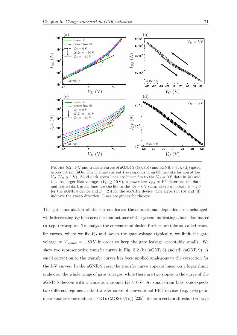
Chapter 5. Charge transport in GNR networks 71
(a)
I DS
(A)
VD (V)
linear fitpower law fit
VG = 0 V
∆VG = −10 V
VG = −50 V
aGNR 5
(b)
I DS
(A)
VG (V)
VD = 5 V
aGNR 5
(c)
I DS
(A)
VD (V)
linear fitpower law fit
VG = 0 V
∆VG = −10 VVG = −50 V
aGNR 9
(d)
I DS
(A)
VG (V)
VD = 5 V
aGNR 9
Figure 5.2: I–V and transfer curves of aGNR 5 ((a), (b)) and aGNR 9 ((c), (d)) gatedacross 300 nm SiO2. The channel current IDS responds in an Ohmic–like fashion at lowVD (VD ≤ 1 V). Solid dark green lines are linear fits to the VG = 0 V data in (a) and(c). At larger bias voltages (VD ≥ 10 V), a power law IDS ∝ V β describes the dataand dotted dark green lines are the fits to the VG = 0 V data, where we obtain β = 2.6for the aGNR 5 device and β = 2.4 for the aGNR 9 device. The arrows in (b) and (d)indicate the sweep direction. Lines are guides for the eye.
The gate modulation of the current leaves these functional dependencies unchanged,
while decreasing VG increases the conductance of the system, indicating a hole–dominated
(p–type) transport. To analyze the current modulation further, we take so–called trans-
fer curves, where we fix VD and sweep the gate voltage (typically, we limit the gate
voltage to VG,max = ±80 V in order to keep the gate leakage acceptably small). We
show two representative transfer curves in Fig. 5.2 (b) (aGNR 5) and (d) (aGNR 9). A
small correction to the transfer curves has been applied analogous to the correction for
the I–V curves. In the aGNR 9 case, the transfer curve appears linear on a logarithmic
scale over the whole range of gate voltages, while there are two slopes in the curve of the
aGNR 5 devices with a transition around VG ≈ 0 V. At small drain bias, one expects
two different regimes in the transfer curve of conventional FET devices (e.g. n–type in
metal–oxide–semiconductor FETs (MOSFETs)) [225]: Below a certain threshold voltage
Chapter 5. Charge transport in GNR networks 72
VG < VT , the current rises exponentially and the transistor operates in the subthreshold
regime. Above threshold, the current eventually rises linearly with increasing VG. Using
this threshold voltage we find in ideal transistors that the gate voltage has the full control
over IDS and the influence of the drain voltage becomes insignificant, when the condition
VDS ≥ (VG−VT ) is met (current saturation) [225]. As visible from Fig. 5.2 (b) and (d),
the saturation regime is not reached in our tested devices and the devices always operate
subthreshold. Therefore, an important figure of merit for transistors, the Ion/Ioff–ratio
is not well–defined in this case. The Ion/Ioff–ratio compares the current in the saturation
regime (on–state) with the current in the subthreshold regime (off–state). In order to
still be able to quantify the impact of the gate voltage, we therefore use two alterna-
tive figures. First, we define a current modulation ratio IM VG,1,VG,2 = I(VG,1)/I(VG,2),
where we compute the ratio of channel current at specific gate voltages and second, we
determine the exponential slope in the range of negative gate voltages. The latter is also
known as subthreshold slope and its inverse is the subthreshold swing [225]
SS =
(∂ log10 IDS
∂VG
)−1
. (5.2)
The subthreshold swing indicates how much gate voltage is required to change the
channel current by a factor ten (one decade ≡ 1 dec). Furthermore, the transfer curves
allow for the determination of a field–effect mobility µFE according to Ref. [226] as
µFE =g
VD COx
L
W. (5.3)
In Eq. 5.3, g = ∂ISD∂VG
is the transconductance, L is the channel length, W is the channel
width and COx = ε ε0/tOx ≈ 1.15 × 10⁻⁴ F/m2 is the geometrical capacitance density
assuming that the channel and the gate electrode form a parallel plate capacitor.3 We use
these definitions to determine IM−80V,+80V ≈ 5 (IM−60V,+60V ≈ 120), SS ≈ 199 V/dec
(SS ≈ 56 V/dec) and µFE ≈ 2 × 10⁻² cm2 V−1 s−1 (µFE ≈ 1 × 10⁻³ cm2 V−1 s−1) for
the aGNR 5 (aGNR 9) device shown in Fig. 5.2 (see Sec. B.4 for more details on the
determination of µFE). We note that we ascertain the channel current to be always
much larger than the gate leakage current in order to avoid artifacts such as transient
off–currents that dip below the gate current and lead to inflated current modulation
ratios.
3Here, we use tOx = 300 nm as mentioned above, the relative permittivity of SiO2 ε = 3.9 and thevacuum permittivity ε0 ≈ 8.854 F/m.
Chapter 5. Charge transport in GNR networks 73
While for aGNR 5 there is no literature available on lateral charge transport experi-
ments, the current modulation for aGNR 9 is comparable to what has been observed
previously [222], although our study does not aim to maximize the device performance.
From a device engineering point of view, there are alternatives to the 300 nm thick
SiO2 gate barrier to drastically improve the electrostatic coupling between the gate elec-
trode and the GNR channel by increasing the electric field at the contacts and improve
the transmission through the barriers. Such alternatives can be found in ionic liquids
(e.g. N, N-diethyl-N-(2-methoxyethyl)-N-methylammonium bis(trifluoromethylsulfonyl-
imide)) or a gate barrier material with a large relative permittivity (e.g. Hafnium dioxide
HfO2). In Ref. [222], Llinas et al. have shown for aGNR 9 that the gate modulation can
be increased from a level comparable to what we find up to a current modulation ratio
of 105. The hysteresis that is present in the transfer curves (Fig. 5.2 (b) and (d)) is also
comparable to previous studies in GNR– or CNT–based devices. Such hysteresis often
arises from charge transfer between carbon materials and charge traps at the silicon
dioxide/ambient interface [227, 228]. While a detailed analysis is beyond the scope of
the present work, it can be found in Ref. [229] and in the following we use averaged
curves of back and forward sweeps for any further analysis. Hysteresis in the I–V curves
(Fig. 5.2 (a) and (c)) was negligible throughout all measurements.
The optimization of the fabrication process (described in the previous section, Sec. 4)
eventually enabled us to produce a larger number of functional devices, in total 97.
Therefore, a comparison of all devices, which have been produced following the fabrica-
tion route 2.A, is possible and we can corroborate the reproducibility and uniformity of
the GNR films as seen by Raman spectroscopy (see Fig. A.1). The statistical analysis
of the electrical characterization furthermore allows us to discriminate between charge
transport signatures which appear systematically and hence are likely to be significant,
and those signatures which occur randomly, for example in the case of local inhomo-
geneities in the GNR film, resulting in a degraded device performance. In Tab. 5.1, we
present the statistics for chip 3 of the aGNR 5 series together with the statistics of chip
3 of the aGNR 9 series.4
4I thank A. T. for his support with the room temperature measurements, increasing the statisticalsample and rendering the statistics more robust.
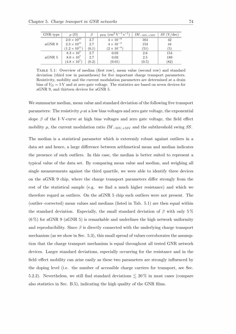
Chapter 5. Charge transport in GNR networks 74
GNR type ρ (Ω) β µFE (cm2 V−1 s−1) IM−50V,+50V SS (V/dec)
aGNR 92.0 × 10¹¹ 2.7 4 × 10⁻⁴ 164 422.3 × 10¹¹ 2.7 4 × 10⁻⁴ 153 44
(1.2 × 10¹¹) (0.1) (2 × 10⁻⁴) (51) (5)
aGNR 58.3 × 10⁷ 2.7 0.03 2.6 1548.0 × 107 2.7 0.03 2.5 189
(4.8 × 10⁷) (0.2) (0.01) (0.5) (82)
Table 5.1: Overview of median (first row), mean value (second row) and standarddeviation (third row in parantheses) for five important charge transport parameters.Resistivity, mobility and the current modulation parameters are determined at a drainbias of VD = 5 V and at zero gate voltage. The statistics are based on seven devices foraGNR 9, and thirteen devices for aGNR 5.
We summarize median, mean value and standard deviation of the following five transport
parameters: The resistivity ρ at a low bias voltages and zero gate voltage, the exponential
slope β of the I–V-curve at high bias voltages and zero gate voltage, the field effect
mobility µ, the current modulation ratio IM−55V,+55V and the subthreshold swing SS .
The median is a statistical parameter which is exteremly robust against outliers in a
data set and hence, a large difference between arithmetical mean and median indicates
the presence of such outliers. In this case, the median is better suited to represent a
typical value of the data set. By comparing mean value and median, and weighing all
single measurements against the third quartile, we were able to identify three devices
on the aGNR 9 chip, where the charge transport parameters differ strongly from the
rest of the statistical sample (e.g. we find a much higher resistance) and which we
therefore regard as outliers. On the aGNR 5 chip such outliers were not present. The
(outlier–corrected) mean values and medians (listed in Tab. 5.1) are then equal within
the standard deviation. Especially, the small standard deviation of β with only 5 %
(6 %) for aGNR 9 (aGNR 5) is remarkable and underlines the high network uniformity
and reproducibility. Since β is directly connected with the underlying charge transport
mechanism (as we show in Sec. 5.3), this small spread of values corroborates the assump-
tion that the charge transport mechanism is equal throughout all tested GNR network
devices. Larger standard deviations, especially occurring for the resistance and in the
field–effect mobility can arise easily as these two parameters are strongly influenced by
the doping level (i.e. the number of accessible charge carriers for transport, see Sec.
5.2.2). Nevertheless, we still find standard deviations . 20 % in most cases (compare
also statistics in Sec. B.5), indicating the high quality of the GNR films.
Chapter 5. Charge transport in GNR networks 75
Based on this analysis, we find a significant difference in the resistance, the mobility and
the current modulation between aGNR 9 and aGNR 5 devices, where we calculate the re-
sistivity as ρ = (VD/IDS) (nW/L), with n, the number of transferred layers, W (L), the
width (length) of the device channel and VD = 5 V. On the basis of Raman spectroscopy
and reported scanning tunneling microsopy images [184, 185], we can assume the aGNR
5 and aGNR 9 networks to be structurally comparable, i.e. the GNRs have on average
the same length and are similarly distributed. Furthermore, the extrinsic charge carrier
density provided by dopants will be similar, since the fabrication process and substrates
are equal. Then, the most relevant expected difference between them is the electronic
structure (compare Sec. 2.2.3.1), e.g. the band gap. Density functional theory predicts
a difference of 400 meV between the band gaps ∆ of aGNR 9 (∆ ≈ 2.1 eV) and aGNR 5
(∆ ≈ 1.7 eV) [6]. Using the conventional exponential dependence of thermally activated
(intrinsic) charge carriers
n ∝ exp
(− ∆
2 kB T
), (5.4)
this difference translates to a factor of 103 at room temperature between the intrinsic
charge carrier densities of the two GNR species (kB is the Boltzmann constant). A
large difference in the charge carrier density is experimentally supported by the gate
voltage–induced current modulation, for which we can calculate the induced charge
carrier density as
nind =COx VG
e, (5.5)
where e is the elementary charge. At VG = 50 V, Eq. 5.5 yields nind ≈ 3.6× 1012 cm−2
and in the aGNR 9 devices, since the current modulation is large, this gate voltage–
induced charge carrier density must be dominant over the background charge carrier
density.5 On the other hand, IM−50V,+50V for aGNR 5 devices is much smaller and
therefore, the induced carrier density can only impose a small change relative to the
total charge carrier density. In Sec. B.6, we directly estimate the total charge carrier
density using the linear part of the I–V curve and Ohm’s law, corroborating this reason-
ing. Nevertheless, at room temperature (300 K), we still have 1.7 eV kB T ≈ 26 meV,
and hence, it appears unintuitive that a charge carrier density in the order of 1012 cm−2
is provided intrinsically, as even the zero–band gap material graphene has not more than
1011 cm−2 intrinsic carriers at room temperature [230]. To explain our observations, two
5This statement is only true, if the contact resistance plays no role. See Sec. 5.2.3 for the influenceof the contacts.
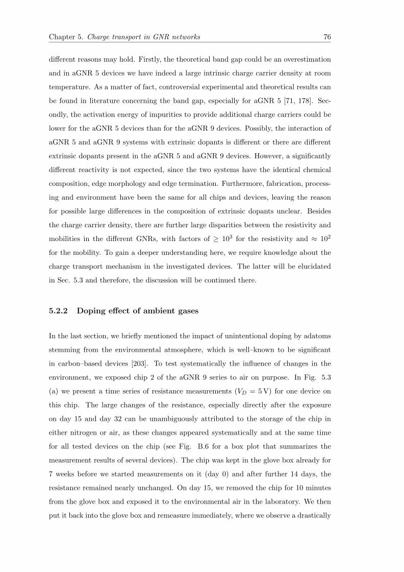
Chapter 5. Charge transport in GNR networks 76
different reasons may hold. Firstly, the theoretical band gap could be an overestimation
and in aGNR 5 devices we have indeed a large intrinsic charge carrier density at room
temperature. As a matter of fact, controversial experimental and theoretical results can
be found in literature concerning the band gap, especially for aGNR 5 [71, 178]. Sec-
ondly, the activation energy of impurities to provide additional charge carriers could be
lower for the aGNR 5 devices than for the aGNR 9 devices. Possibly, the interaction of
aGNR 5 and aGNR 9 systems with extrinsic dopants is different or there are different
extrinsic dopants present in the aGNR 5 and aGNR 9 devices. However, a significantly
different reactivity is not expected, since the two systems have the identical chemical
composition, edge morphology and edge termination. Furthermore, fabrication, process-
ing and environment have been the same for all chips and devices, leaving the reason
for possible large differences in the composition of extrinsic dopants unclear. Besides
the charge carrier density, there are further large disparities between the resistivity and
mobilities in the different GNRs, with factors of ≥ 103 for the resistivity and ≈ 102
for the mobility. To gain a deeper understanding here, we require knowledge about the
charge transport mechanism in the investigated devices. The latter will be elucidated
in Sec. 5.3 and therefore, the discussion will be continued there.
5.2.2 Doping effect of ambient gases
In the last section, we briefly mentioned the impact of unintentional doping by adatoms
stemming from the environmental atmosphere, which is well–known to be significant
in carbon–based devices [203]. To test systematically the influence of changes in the
environment, we exposed chip 2 of the aGNR 9 series to air on purpose. In Fig. 5.3
(a) we present a time series of resistance measurements (VD = 5 V) for one device on
this chip. The large changes of the resistance, especially directly after the exposure
on day 15 and day 32 can be unambiguously attributed to the storage of the chip in
either nitrogen or air, as these changes appeared systematically and at the same time
for all tested devices on the chip (see Fig. B.6 for a box plot that summarizes the
measurement results of several devices). The chip was kept in the glove box already for
7 weeks before we started measurements on it (day 0) and after further 14 days, the
resistance remained nearly unchanged. On day 15, we removed the chip for 10 minutes
from the glove box and exposed it to the environmental air in the laboratory. We then
put it back into the glove box and remeasure immediately, where we observe a drastically
Chapter 5. Charge transport in GNR networks 77
(a)
Time (days)
Res
ista
nce
(Ω)
Firstexposure
Secondexposure
(b)
VG (V)
I DS
(A)
day 14
day 15 (afterair exposure)
∆VG
Figure 5.3: Impact of ambient doping on the electrical properties of GNR networkFETs. In (a), we plot the resistance of a aGNR 9 device as a function of time. Thejumps in the resistance can unambiguously traced back to the exposure to air. Withthe help of the change in the transfer curves, shown in (b), we estimate the change ofcharge carrier density to ∆n ≈ 1.8× 1012 cm−2. Lines are guides for the eye.
enhanced current, about 18 times as large as before, i.e. a much lower resistance. After
12 additional days, the pre-exposure value of the device resistance is nearly restored.
On day 32, we again remove the chip from the glove box and this time, we expose it for
5.5 hours to the laboratory air. Remeasuring shows that again the resistance is lowered
(approximately by a factor of 12). However, the reverse process, presumably associated
with the desorption of adatoms in the inert gas atmosphere, has begun immediately
after the air exposure ended, as shown by the fact that the resistance has nearly tripled
24 hours after ending the exposure to air.
By looking at the transfer characteristics before and after exposure (see Fig. 5.3 (b)), we
can estimate how many charges have been introduced due to the air exposure. For that,
we shift the post exposure curve by ∆VG ≈ 25 V such that it coincides with the pre–
exposure curve. Via Eq. 5.5, this difference in gate voltage translates into a change of the
surface charge carrier density of ∆n ≈ 1.8×1012 cm−2, resulting in larger conductances.
Especially at large positive gate voltages, where we induce electrons and deplete holes,
the ratio Ipost−exp/Ipre−exp (at constant VG and VD) grows. As a consequence, the
current modulation ratio and the subthreshold swing are notably affected, where the
former drops from IM−55V,+55V ≈ 3×10² to IM−55V,+55V ≈ 1×10² and the latter rises
from SS ≈ 41 V/dec to SS ≈ 52 V/dec.
Chapter 5. Charge transport in GNR networks 78
The presented results of our experiments are extremenly important to understand how
unintenional doping can affect the device performance in any charge transport exper-
iment with graphene nanoribbons. Some parts of the fabrication process usually take
place in the laboratory or in a cleanroom, where it is not possible to exactly control
the environmental gas composition. Different gaseous species contained in normal air,
such as oxygen and water, can contaminate the sample surface during and after the
fabrication and typically result in p–type doping [203]. Hence, in an ideal fabrication
process, the GNRs should never be exposed to air. However, meeting this require-
ment is technologically complex and usually costly, although performing fabrication and
measurements in a controlled inert gas atmosphere is fundamentally possible. As an
alternative, annealing, e.g. by passing large current densities through the device [231]
or heating in a gas mixture of hydrogen and argon has been suggested and tested in
charge transport experiments in graphene–based devices [203]. However, employing the
deposition process as discussed in Sec. 4.2.2, adsorbates can be trapped between the
substrate and GNR film and in this case, annealing will not necessarily lead to a removal
of these impurities. In Fig. B.7, we show that current annealing is possible with our de-
vices. However, the major scope of this work is to shed light on the fundamental charge
transport properties. Hence, we leave room for follow–up studies to further engineer
the device fabrication process and annealing procedures towards the minimization of
unintentional doping, while we focus on the in–depth analysis of the underlying charge
transport mechanisms in our devices in the following sections.
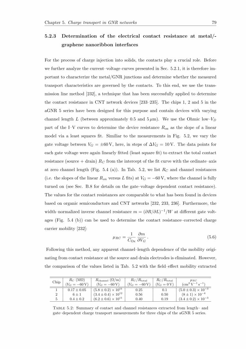
Chapter 5. Charge transport in GNR networks 79
5.2.3 Determination of the electrical contact resistance at metal/-
graphene nanoribbon interfaces
For the process of charge injection into solids, the contacts play a crucial role. Before
we further analyze the current–voltage curves presented in Sec. 5.2.1, it is therefore im-
portant to characterize the metal/GNR junctions and determine whether the measured
transport characteristics are governed by the contacts. To this end, we use the trans-
mission line method [232], a technique that has been successfully applied to determine
the contact resistance in CNT network devices [233–235]. The chips 1, 2 and 5 in the
aGNR 5 series have been designed for this purpose and contain devices with varying
channel length L (between approximately 0.5 and 5µm). We use the Ohmic low–VD
part of the I–V curves to determine the device resistance Ron as the slope of a linear
model via a least squares fit. Similiar to the measurements in Fig. 5.2, we vary the
gate voltage between VG = ±60 V, here, in steps of ∆VG = 10 V. The data points for
each gate voltage were again linearly fitted (least square fit) to extract the total contact
resistance (source + drain) RC from the intercept of the fit curve with the ordinate–axis
at zero channel length (Fig. 5.4 (a)). In Tab. 5.2, we list RC and channel resistances
(i.e. the slopes of the linear Ron versus L fits) at VG = −60 V, where the channel is fully
turned on (see Sec. B.8 for details on the gate–voltage dependent contact resistance).
The values for the contact resistances are comparable to what has been found in devices
based on organic semiconductors and CNT networks [232, 233, 236]. Furthermore, the
width–normalized inverse channel resistance m = (∂R/∂L)−1/W at different gate volt-
ages (Fig. 5.4 (b)) can be used to determine the contact resistance–corrected charge
carrier mobility [232]:
µRC =1
COx
∂m
∂VG. (5.6)
Following this method, any apparent channel–length dependence of the mobility origi-
nating from contact resistance at the source and drain electrodes is eliminated. However,
the comparison of the values listed in Tab. 5.2 with the field–effect mobility extracted
ChipRC (MΩ) Rchannel (Ω/m) RC/Rtotal RC/Rtotal µRC
(VG = −60 V) (VG = −60 V) (VG = −60 V) (VG = 0 V) (cm2 V−1 s−1)
1 0.17 ± 0.05 (5.8 ± 0.2) × 1011 0.25 0.1 (5.0 ± 0.3) × 10−3
2 6 ± 1 (3.4 ± 0.4) × 1012 0.56 0.50 (8 ± 1) × 10−4
5 0.4 ± 0.2 (6.2 ± 0.6) × 1011 0.40 0.19 (3.4 ± 0.2) × 10−3
Table 5.2: Summary of contact and channel resistances extracted from length– andgate–dependent charge transport measurements for three chips of the aGNR 5 series.
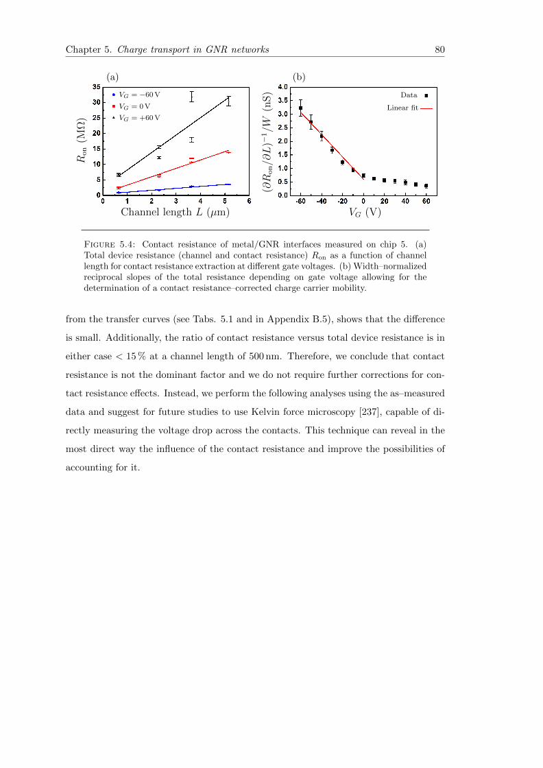
Chapter 5. Charge transport in GNR networks 80
(a)
Channel length L (µm)
Ron
(MΩ
)VG = −60 V
VG = 0 V
VG = +60 V
(b)
VG (V)
(∂R
on/∂L
)−1/W
(nS) Data
Linear fit
Figure 5.4: Contact resistance of metal/GNR interfaces measured on chip 5. (a)Total device resistance (channel and contact resistance) Ron as a function of channellength for contact resistance extraction at different gate voltages. (b) Width–normalizedreciprocal slopes of the total resistance depending on gate voltage allowing for thedetermination of a contact resistance–corrected charge carrier mobility.
from the transfer curves (see Tabs. 5.1 and in Appendix B.5), shows that the difference
is small. Additionally, the ratio of contact resistance versus total device resistance is in
either case < 15 % at a channel length of 500 nm. Therefore, we conclude that contact
resistance is not the dominant factor and we do not require further corrections for con-
tact resistance effects. Instead, we perform the following analyses using the as–measured
data and suggest for future studies to use Kelvin force microscopy [237], capable of di-
rectly measuring the voltage drop across the contacts. This technique can reveal in the
most direct way the influence of the contact resistance and improve the possibilities of
accounting for it.
Chapter 5. Charge transport in GNR networks 81
5.3 Charge transport mechanism in graphene nanoribbon
networks
5.3.1 Universal scaling of charge transport
We can now attempt a thorough analysis of charge transport in aGNR 5 and aGNR 9
networks.6 A priori the charge transport mechanism is not clear in our systems. The
GNRs themselves are crystalline units and in crystalline materials, charge carriers are
delocalized, where Bloch waves in the band structure picture are a proper description.
On the other hand, dealing with networks of GNR units, where charge carriers have to
cross ribbon–ribbon junctions, suggests that hopping between GNRs should be consid-
ered alternatively to be the dominant transport mechanism, very similar to the situation
in most organic semiconductors [104]. Generally, the temperature dependence of charge
transport can help to identify the appropriate mechanism. Therefore, we measure one
aGNR 5 device and one aGNR 9 device in a cryostat (see Sec. 3.2.2), where we vary the
temperature between 260 K and approximately 3 K and take I–V curves at various fixed
temperatures as shown in Fig. 5.5 (a) and (b). In the double logarithmic plot of the
I–V curves, we observe two general trends: The current decreases monotonously with
decreasing temperature, and the transition voltage from linear to superlinear behavior
decreases with decreasing temperature. At large biases, the functional dependence re-
mains a power law, however the exponent β changes and extrapolation to T → 0 yields
values of β = 4 (β = 8) for the aGNR 5 (aGNR 9) device. Similar power laws have been
obsverved for a large range of semiconducting polymers [100, 101] and can be explained
by nuclear tunneling mediated hopping as the dominant charge transport mechanism.
In nuclear tunneling, the coupling of the electronic charges to their nuclear environment
sets the potential landscape for the movement of the charges. As detailed in Sec. 2.3, an
analytic expression for the expected current (Eqs. 2.29, 2.30 and 2.31) can be derived if
all hopping events are assumed to be equivalent, which is the case when energetic disor-
der is suppressed by high charge carrier densities. However, it is important to note that
there are other physical models which yield Eq. 2.29. Among these models we can rule
out Luttinger Liquid [238] since it requires impurity–free purely one–dimensional sys-
tems, and Coulomb blockade, which we expect for transport through a low–capacitance
6I sincerely thank Dr. K. A. and Prof. Dr. P. B. for the stimulating discussions about the dataanalysis presented in this chapter.
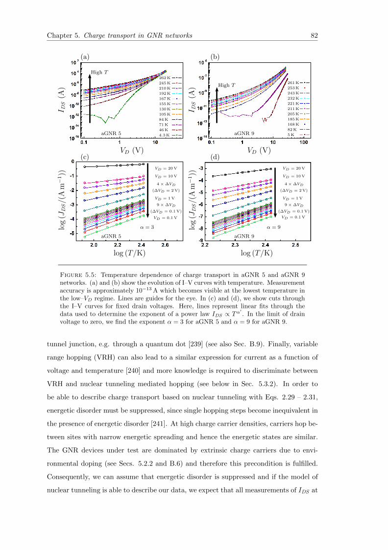
Chapter 5. Charge transport in GNR networks 82
(a)I D
S(A
)
VD (V)
High T262 K
245 K
210 K
192 K
167 K
155 K
130 K
105 K
84 K
71 K
46 K
4.3 KaGNR 5
(b)
I DS
(A)
VD (V)
High T261 K
253 K
243 K
232 K
221 K
211 K
205 K
185 K
168 K
82 K
5 KaGNR 9
(c)
log
(JDS/(
Am−
1))
log (T/K)
VD = 20 V
VD = 10 V
4×∆VD
(∆VD = 2 V)
VD = 1 V
9×∆VD
(∆VD = 0.1 V)
VD = 0.1 V
α = 3
aGNR 5
(d)
log
(JDS/(
Am−
1))
log (T/K)
VD = 20 V
VD = 10 V
4×∆VD
(∆VD = 2 V)
VD = 1 V
9×∆VD
(∆VD = 0.1 V)
VD = 0.1 V
α = 9
aGNR 9
Figure 5.5: Temperature dependence of charge transport in aGNR 5 and aGNR 9networks. (a) and (b) show the evolution of I–V curves with temperature. Measurementaccuracy is approximately 10−13 A which becomes visible at the lowest temperature inthe low–VD regime. Lines are guides for the eye. In (c) and (d), we show cuts throughthe I–V curves for fixed drain voltages. Here, lines represent linear fits through thedata used to determine the exponent of a power law IDS ∝ Tα
′. In the limit of drain
voltage to zero, we find the exponent α = 3 for aGNR 5 and α = 9 for aGNR 9.
tunnel junction, e.g. through a quantum dot [239] (see also Sec. B.9). Finally, variable
range hopping (VRH) can also lead to a similar expression for current as a function of
voltage and temperature [240] and more knowledge is required to discriminate between
VRH and nuclear tunneling mediated hopping (see below in Sec. 5.3.2). In order to
be able to describe charge transport based on nuclear tunneling with Eqs. 2.29 – 2.31,
energetic disorder must be suppressed, since single hopping steps become inequivalent in
the presence of energetic disorder [241]. At high charge carrier densities, carriers hop be-
tween sites with narrow energetic spreading and hence the energetic states are similar.
The GNR devices under test are dominated by extrinsic charge carriers due to envi-
ronmental doping (see Secs. 5.2.2 and B.6) and therefore this precondition is fulfilled.
Consequently, we can assume that energetic disorder is suppressed and if the model of
nuclear tunneling is able to describe our data, we expect that all measurements of IDS at
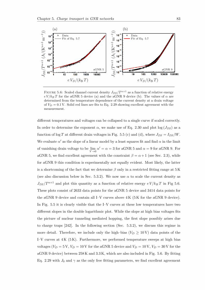
Chapter 5. Charge transport in GNR networks 83
(a)
e VD/(kB T )
JDS/T
α+
1(A/(
Kα
+1
m−
1))
aGNR 5
DataFit of Eq. 5.7
(b)
e VD/(kB T )
JDS/T
α+
1(A/(
Kα
+1
m−
1))
aGNR 9
DataFit of Eq. 5.7
Figure 5.6: Scaled channel current density JDS/Tα+1 as a function of relative energy
e V/kB T for the aGNR 5 device (a) and the aGNR 9 device (b). The values of α aredetermined from the temperature dependence of the current density at a drain voltageof VD = 0.1 V. Solid red lines are fits to Eq. 2.29 showing excellent agreement with themeasurement.
different temperatures and voltages can be collapsed to a single curve if scaled correctly.
In order to determine the exponent α, we make use of Eq. 2.30 and plot log (JDS ) as a
function of log T at different drain voltages in Fig. 5.5 (c) and (d), where JDS = IDS/W .
We evaluate α′ as the slope of a linear model by a least squares fit and find α in the limit
of vanishing drain voltage to be limV→0
α′ = α = 3 for aGNR 5 and α = 9 for aGNR 9. For
aGNR 5, we find excellent agreement with the constraint β = α+ 1 (see Sec. 2.3), while
for aGNR 9 this condition is experimentally not equally evident. Most likely, the latter
is a shortcoming of the fact that we determine β only in a restricted fitting range at 5 K
(see also discussion below in Sec. 5.3.2). We now use α to scale the current density as
JDS/Tα+1 and plot this quantity as a function of relative energy e V/kB T in Fig 5.6.
These plots consist of 2633 data points for the aGNR 5 device and 3414 data points for
the aGNR 9 device and contain all I–V curves above 4 K (5 K for the aGNR 9 device).
In Fig. 5.5 it is clearly visible that the I–V curves at these low temperatures have two
different slopes in the double logarithmic plot. While the slope at high bias voltages fits
the picture of nuclear tunneling mediated hopping, the first slope possibly arises due
to charge traps [242]. In the following section (Sec. 5.3.2), we discuss this regime in
more detail. Therefore, we include only the high–bias (VD ≥ 10 V) data points of the
I–V curves at 4 K (5 K). Furthermore, we performed temperature sweeps at high bias
voltages (VD = 5 V, VD = 10 V for the aGNR 5 device and VD = 10 V, VD = 30 V for the
aGNR 9 device) between 258 K and 3.3 K, which are also included in Fig. 5.6. By fitting
Eq. 2.29 with J0 and γ as the only free fitting parameters, we find excellent agreement
Chapter 5. Charge transport in GNR networks 84
using J0 = (1.44± 0.05)× 10−12 A/(Kα+1 m−1), γ = (7.66± 0.09)× 10−3 for the aGNR
5 device and J0 = (2.1 ± 0.1) × 10−32 A/(Kα+1 m−1), γ = (4.84 ± 0.04) × 10−3 for the
aGNR 9 device. The parameter γ is expected to be dependent on channel length [100],
while α and J0 are expected to be constant. Studying these parameters as a function of
L will help to further pin down the details of charge transport, e.g. to test VRH against
nuclear tunneling mediated hopping.
After having established that charge hopping is likely the dominant charge transport
mechanism, we can again look at the values for the mobility as determined in Sec.
5.2.1. Although a degradation of the charge carrier mobility with larger band gaps
is expected, theory predicts still much larger values for the mobility in the order of
102 cm2 V−1 s−1 for GNRs with a band gap of comparable size [243]. Using terahertz
spectroscopy, comparable values have been experimentally observed in aGNR 9 samples
[184]. However, in the field of semiconducting polymer devices, mobilities in the range
of 10−1 cm2 V−1 s−1 to 10−4 cm2 V−1 s−1 are typically observed [244], where hopping is
regularly the dominant charge transport mechanism. In this case the current (i.e. the
resistivity) as well as the mobility are determined by the hopping rates (compare Eq.
2.32 in Sec. 2.3). The rate equation in the dissipative case of nuclear tunneling has
been derived in Sec. 2.3 and hence, instead of scattering events of delocalized electron
waves, the microscopic parameters in Eq. 2.26 determine the mobility and resistivity.
The experimentally determined parameter α is a scaled version of the Kondo parameter
as described in Sec. 2.3 and we see that based on this parameter, the coupling between
charges and bath is stronger in aGNR 9 (α = 9) than in aGNR 5 (α = 3). The other
quantities in Eq. 2.26 can be accessed eventually by further measurements beyond the
scope of this work as, for example, the energy difference between donors and acceptors
εij is directly related to the channel length dependence of γ (compare also Eq. 2.28 in
Sec. 2.3). To substantiate the generality of this analysis, these experiments should be
repeated with other types of GNRs, e.g. aGNR 7 or aGNR 13, which belong the aGNR
N = 3m+1 family in contrast to aGNR 5 and aGNR 9 which belong to the 3m+2 and
3m families, respectivley (see also Sec. 2.2.3.1). Then we expect a renormalization of
the I(V, T ) characteristics according to Eq. 2.29 will collapse for all GNR species onto
a single curve. For this renormalization, although beyond the scope of this work, the
dimensionless parameter e Vhop/(kB T ), with Vhop = γ V , representing the applied bias
divided by the number of hops can be used in analogy to Ref. [100].
Chapter 5. Charge transport in GNR networks 85
5.3.2 Transport at low bias and low temperature
As mentioned in the previous section, the I–V curves of both, the aGNR 5 and the
aGNR 9 device, show at 4 K and 5 K a qualitative difference to the I–V curves at more
elevated temperatures. For low bias voltages, there is a different slope in the log IDS
vs. log VD data at such low temperatures as shown in Fig. 5.7 (a) and (b). Such
an additional slope in the I–V characteristic is typical for the presence of charge traps
[242]. The second slope at large drain voltages fits again the trend of the I–V curves
at higher temperatures. For the aGNR 5 device, we find a peculiar dependence of the
resistance on a perpendicularly applied magnetic field (see Fig. 5.7 (c) and (d)). At
low bias voltages, we observe an increase of the resistance with magnetic field B up to
a relative change of 14 % at B = 8 T which can be perfectly described by a quadratic
function ∆ρ/ρ = aB2. Although, this behavior is reminiscent of the ordinary Kohler
magnetoresistance in metals [245], this model is inadequate as it is based on delocalized
band transport and the transport mechanism here is clearly charge carrier hopping.
To investigate this effect further, we study it as a function of temperature and bias
voltage. Increasing these parameters leads to a decrease of the effect. In Fig. 5.7
(d), we see that no magnetic field dependence can be seen anymore above T = 50 K.
Furthermore, when we increase the bias voltage and approach the regime of nuclear
tunneling mediated hopping, the effect also goes down, as shown in Fig. 5.7 (c), where we
present magnetic field sweeps at two different drain voltages of VD = 5 V and VD = 10 V.
A model to explain these intriguing findings is elusive and our result is contrary to
previous studies, which found a large negative magnetoresistance effect in graphene
nanostructures [224]. However, the experiments of Bai et al. in Ref. [224] deal with
top–down patterned single ribbon devices operating in a Coulomb blockade regime. In
contrast, hopping transport is in general compatible with a positive magnetoresistance
where, however, an exponential dependence of the resistance with magnetic field is
expected instead of a power law [246]. Hence, in order to understand the effect in more
detail, further measurements are required. First, the parameter space of bias voltage,
temperature and magnetic field should be scanned with higher precision, which allows to
follow better the transition of the nuclear tunneling regime into the magnetoresistance
regime. Second, the measurements should be extended to higher magnetic fields, to test
different predictions for the magnetoresistance [246].
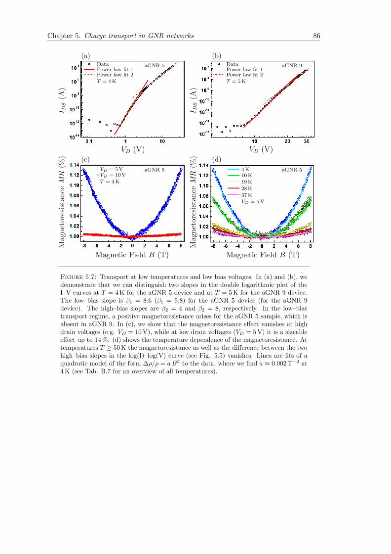
Chapter 5. Charge transport in GNR networks 86
(a)I D
S(A
)
VD (V)
DataPower law fit 1Power law fit 2
T = 4 K
aGNR 5
(b)
I DS
(A)
VD (V)
DataPower law fit 1Power law fit 2
T = 5 K
aGNR 9
(c)
Mag
net
ores
ista
nce
MR
(%)
Magnetic Field B (T)
VD = 5 VVD = 10 VT = 4 K
aGNR 5
(d)
Mag
net
ores
ista
nce
MR
(%)
Magnetic Field B (T)
4 K10 K19 K
28 K
37 KVD = 5 V
aGNR 5
Figure 5.7: Transport at low temperatures and low bias voltages. In (a) and (b), wedemonstrate that we can distinguish two slopes in the double logarithmic plot of theI–V curves at T = 4 K for the aGNR 5 device and at T = 5 K for the aGNR 9 device.The low–bias slope is β1 = 8.6 (β1 = 9.8) for the aGNR 5 device (for the aGNR 9device). The high–bias slopes are β2 = 4 and β2 = 8, respectively. In the low–biastransport regime, a positive magnetoresistance arises for the aGNR 5 sample, which isabsent in aGNR 9. In (c), we show that the magnetoresistance effect vanishes at highdrain voltages (e.g. VD = 10 V), while at low drain voltages (VD = 5 V) it is a sizeableeffect up to 14 %. (d) shows the temperature dependence of the magnetoresistance. Attemperatures T ≥ 50 K the magnetoresistance as well as the difference between the twohigh–bias slopes in the log(I)–log(V) curve (see Fig. 5.5) vanishes. Lines are fits of aquadratic model of the form ∆ρ/ρ = aB2 to the data, where we find a ≈ 0.002 T−2 at4 K (see Tab. B.7 for an overview of all temperatures).
...
Chapter 5. Charge transport in GNR networks 87
5.4 Conclusion and outlook
In conclusion, we have shown that for aGNR 5 and aGNR 9 network FET devices at high
charge carrier densities, the I(V, T ) characteristics over a wide range of temperatures and
bias voltages can be described by the unified description developed for semiconducting
polymers, which includes the hopping rates derived by the model of nuclear tunnelling.
For both types of GNRs, aGNRs 5 and aGNRs 9, the I(V, T ) characteristics showed a
power law dependence on both temperature and voltage which can be renormalized to a
single curve. This universal curve integrates all measurements at temperatures between
3 and 260 K and at drain voltages swept over two orders of magnitude. This study shows
that the mechanism that drives charge transport in all organic polymer devices is also
operational in devices based on GNR networks.
However, there are still open questions calling for further experimental and theoretical
work beyond the current work. These open questions for example concern the actual
band gap for lateral charge transport or the role of charge traps for the large positive
magnetoresistance in aGNR 5. By analyzing the hysteresis of the transfer curves, it
will be possible to infer the number of charge traps in the devices (this is subject of a
follow–up study in Ref. [229]). However, their role to influence the effect of a magnetic
field is unclear at the moment. Furthermore, due to the current state–of–the–art GNR
fabrication, the final transport properties of each sample are determined by a number
of extrinsic factors which cannot be controlled directly. As a consequence, there is al-
ways a random element in the fabrication of GNR FET devices, for instance resistance,
charge carrier mobility or the current modulation ratio of two GNR samples fabricated
together under exactly the same conditions may differ by as much as a factor of two.
Consequently, it is an absolute necessity to repeat the experiments on several samples to
exclude sample–dependent artifacts and uncertainties. For future experiments, we sug-
gest to rely on encapsulated GNR samples, e.g. sandwiched between sheets of hexagonal
boron nitride, a technique which is nowadays common for devices based on graphene
sheets [247].

Chapter 5. Charge transport in GNR networks 88
Additionally, we suggest it to be worthwhile to optimize the device production fur-
ther towards single–ribbon devices. Firstly, based on the results of our study, charge
transport signatures in short–channel devices can now be interpreted much more facile,
especially in the case of an uncertain number of ribbons forming the conductive channel.
Secondly, with aGNR 5, we have found the most conductive GNR species so far, which
will drastically increase the yield of functional short–channel devices.
Chapter 6
Magnetoresistance and charge
transport in graphene governed
by nitrogen dopants
Substitutional nitrogen doping of graphene is a viable route for the tailoring of charge
carrier properties in graphene. We elucidate the nature of this doping by combining
Raman spectroscopy to obtain structural information, and charge transport measure-
ments, which additionally reveal the influence of charged impurities on the electronic
properties. In a thorough electrical characterization of undoped graphene and nitrogen
doped graphene at variable temperatures and in magnetic fields up to 8 T, we find a
sixfold increase in the charge carrier concentration with varying nitrogen content, indi-
cating highly effective doping. Additionally, the formation of a charge transport gap is
revealed by variable range hopping conduction. The magnetotransport exhibits a con-
spicuous sign change from positive Kohler magnetoresistance in undoped graphene to a
large negative magnetoresistance that we can attribute to the doping induced disorder.
The presented experiments have been the basis of a bachelor thesis (Ref. [248]) and a
publication (Ref. [249]) and the majority of the measurements was performed together
with M. R.. For the following discussion, the analysis of the data has been thoroughly
revised and extended. With these more accurate and new results, we quantify the tran-
sition from weak to strong localization in doped graphene based on the change of the
length scales for phase coherent transport and localization.
89
Chapter 6. Charge transport in nitrogen–doped graphene 90
6.1 Experimental details
For the experiments on doped graphene, ten samples were produced in total and the
three samples with the highest quality were used for measurements. Samples 1 and 2
were provided by the Max Planck Institute for Polymer Research, and are not doped.
Sample 3 stems from a collaboration with an industrial partner and is doped with ni-
trogen. Since the undoped samples are qualitatively similar [248], we show the results
of only one of them (sample 2). All samples have been fabricated by CVD as described
in Sec. 4.1.1. For the doped sample, the nitrogen atoms were incorporated in the lattice
following the approach described in Ref. [149]. For the realization of charge transport
test devices, different approaches have been tested. One possible fabrication strategy
is to transfer the graphene first and define the contacts afterwards. This fabrication
route suffers from mainly two disadvantages: The patterning procedure by EBL gener-
ally leaves resist residues on the graphene surface and can degrade the quality of the
sample. Furthermore, the graphene crystals can get damaged in the metalization pro-
cess, especially when sputtering is used, where metal atoms impinge with high energy
on the graphene surface. Hence, in order to perform charge transport measurements,
silicon/silicondioxide (Si/SiO2) substrates have been prepared with sets of four metallic
contact pads which build the corners of a square with side lenghts between 100 and
800µm. These contact pads were made of gold (thickness tAu ≈ 50 nm), where we used
a chromium seed layer (thickness tCr ≈ 5 nm) to improve adhesion to the SiO2 surface.
The metals have been sputter evaporated onto the SiO2 surface. Prior to the sputtering,
the structures have been defined by EBL. Here, a resist double layer of MMA(8.5)MAA
EL6 and PMMA 950K A3 has been used, facilitating the lift–off procedure compared to
single–layer resist approaches. The fabrication steps in detail are the following:
1. Sample Preparation
• Standard cleaning procedure of Si/SiO2 substrates (highly doped p++ Si with
(300± 5) nm SiO2) as described in Sec. 4.3.1.
• Spin coating of MMA(8.5)MAA EL6 onto the substrate using a prespin of
500 rpm for 5 s and a mainspin of 2000 rpm for 60 s (acceleration of 2000 rps2).
Baking on the hot plate for 90 s at 180C.
Chapter 6. Charge transport in nitrogen–doped graphene 91
• Spin coating of PMMA 950K A3 onto the substrate using a prespin of 500 rpm
for 3 s and a mainspin of 2500 rpm for 60 s (acceleration 2000 rps2). Baking
on the hot plate for 90 s at 180C.
2. EBL step
• Electron beam exposure with a dose of 170µC/cm2 at an acceleration voltage
of 10 kV.
• Development of the structures by immersing the substrate fully into a mixture
of methyl isobutyl ketone and isopropanole (1 : 3) for 30 s and subsequently
into pure isopropanole for 30 s.
3. Metallization by sputtering a Cr/Au film (≈ 5 nm/50 nm) under the same condi-
tions as described in Sec. 4.3.1.
4. Lift–off by immersing the sample into acetone for some hours. Using a pipette to
establish a gentle flow over the surface can accelerate the procedure.
Further details of the fabrication can be found in Ref. [248]. The graphene has not been
further patterned and instead the samples have been measured using the VDP method
(see Sec. 3.2.4). The charge transport experiments have been performed in a helium
bath cryostat using a Keithley 224 current source and a Keithley 182 voltmeter for the
resistance measurements. The theory of the VDP method assumes point–like contacts
and the error induced by the size of the contacts has been considered and is described
in detail in Ref. [248].
Chapter 6. Charge transport in nitrogen–doped graphene 92
6.2 Structural investigation using Raman spectroscopy
The fabrication of graphene using CVD is an established method and has been sig-
nifiantly optimized over the recent years to yield graphene crystals of high structural
integrity and with very good electrical properties as for example demonstrated by a large
values for the charge carrier mobility [160]. On the other hand, the synthesis of doped
graphene species, as described in Sec. 4.1.1, is more difficult to control which results
in a lower reproducibility of sample quality. To ascertain the impact of the CVD dop-
ing procedure, we combine electrical transport and structural investigation by Raman
spectroscopy for each sample. We start with the discussion of the Raman spectra of the
doped and of an undoped graphene sample. For both samples 225 spots on the sample
have been tested (compare Ref. [248]) to check for homogeneity and in Fig. 6.1 we show
two representative spectra. The theoretically expected line shape of the peaks follows
a Lorentzian profile. In practice however, the resolution of the measurement apparatus
can lead to additional Gaussian broadening and therefore, a convolution of a Lorentzian
and a Gaussian distribution function describes the data more accurateley [250]. Such a
convolution is called a Voigt profile and is given by
V (x, σ, γ) =
∫ ∞−∞
G(x′, σ)L(x− x′, γ)dx′ , (6.1)
G(x, σ) =1
σ√
2πe−t
2/2σ2, L(x, γ) = I0
1
1 +(
2 (x−x0)γ
)2 . (6.2)
where G(x, σ) denotes a Gaussian distribution with a standard deviation σ and L(x, γ) is
the Lorentzian Raman line profile centered at x0 and with a full width at half maximum
(FWHM) γ. Evaluating this convolution is computationally expensive and for this reason
the fit to the Raman spectra has been done using an approximation [251] which has a
maximum deviation from Eq. 6.1 of 10−13. The obtained peak positions are summarized
in Tab. 6.1 together with the FWHM of the fit and the peak height normalized to the
G peak. We first analyze these data with respect to the number of layers (N) because
the CVD growth can lead to mixtures of single layer graphene (SLG), bilayer graphene
(BLG) or few–layer graphene (FLG) samples, although the process is self–limited as soon
as the reactive copper surface is covered and the contact with the precursor is blocked
[252]. Albeit Raman spectra of SLG and graphene stacks share some fundamental peaks
like the D, G or 2D peak, shear and layer breathing modes (LBM) are only possible
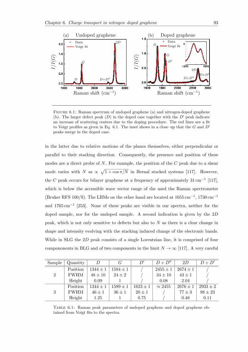
Chapter 6. Charge transport in nitrogen–doped graphene 93
(a) (b)Undoped graphene Doped graphene
I/I
(G)
Raman shift (cm−1)
I/I
(G)
Raman shift (cm−1)
Data
Voigt fit
Data
Voigt fit
D
G
D+D′′
2DD
G
D′
D+D′′
2D
D+D′
Figure 6.1: Raman spectrum of undoped graphene (a) and nitrogen-doped graphene(b). The larger defect peak (D) in the doped case together with the D′ peak indicatean increase of scattering centers due to the doping procedure. The red lines are a fitto Voigt profiles as given in Eq. 6.1. The inset shows in a close–up that the G and D′
peaks merge in the doped case.
in the latter due to relative motions of the planes themselves, either perpendicular or
parallel to their stacking direction. Consequently, the presence and position of these
modes are a direct probe of N . For example, the position of the C peak due to a shear
mode varies with N as ∝√
1 + cosπ/N in Bernal stacked systems [117]. However,
the C peak occurs for bilayer graphene at a frequency of approximately 31 cm−1 [117],
which is below the accessible wave vector range of the used the Raman spectrometer
(Bruker RFS 100/S). The LBMs on the other hand are located at 1655 cm−1, 1730 cm−1
and 1765 cm−1 [253]. None of these peaks are visible in our spectra, neither for the
doped sample, nor for the undoped sample. A second indication is given by the 2D
peak, which is not only sensitive to defects but also to N as there is a clear change in
shape and intensity evolving with the stacking induced change of the electronic bands.
While in SLG the 2D peak consists of a single Lorentzian line, it is comprised of four
compononents in BLG and of two components in the limit N →∞ [117]. A very careful
Sample Quantity D G D′ D +D′′ 2D D +D′
Position 1344± 1 1584± 1 / 2455± 1 2674± 1 /2 FWHM 48± 10 24± 2 / 34± 10 43± 1 /
Height 0.09 1 / 0.08 2.04 /
Position 1344± 1 1589± 1 1623± 1 ≈ 2455 2676± 1 2933± 23 FWHM 46± 1 36± 1 20± 1 / 77± 3 98± 23
Height 1.25 1 0.75 / 0.48 0.11
Table 6.1: Raman peak parameters of undoped graphene and doped graphene ob-tained from Voigt fits to the spectra.
Chapter 6. Charge transport in nitrogen–doped graphene 94
analysis is necessary here because a single Lorentzian fit could also be consistent with
TG [117] and hence this is not a direct evidence for SLG on its own. In this case, a
significant broadening is expected with an FWHM of more than 50 cm−1, roughly two
times larger than in SLG [117]. Looking at the 2D peak in the spectrum of the undoped
sample (Fig. 6.1 (a)) such a broadening is not discernible (i.e. the measured peaks have
a sharp maximum and no shoulder features) and a single Voigt line yields a good fit.
The FWHM of this line is (43 ± 1) cm−1, where the inherent Lorentzian contribution
has an FWHM of (23 ± 1) cm−1. While the Lorentzian FWHM is in good agreement
with the expected value for SLG, the overall line width is larger but still below the value
expected for TG. Structural disorder in the sample can cause an enhanced FWHM, as
well as the Gaussian component induced by the measurement apparatus. Such disorder
is definitely present in the sample as can be inferred from the presence of a D peak.
The same reasoning holds for the 2D FWHM of the doped sample. Here, again a single
Voigt line describes the data resonably well and the FWHM is (77 ± 3) cm−1, where
a strong disorder broadening is expected from the large D peak as detailed below. In
summary, while the described Raman features give a good indication that our samples
are predominantly SLG, minor patches of BLG or FLG cannot be excluded, especially
in the doped case. One of the most direct evidence of SLG would be for example the
observation of SLG–like anomalous quantum Hall effect in a clean sample [254].
Further information about the structural integrity of the samples can be drawn from
the Raman spectra and in particular from the D peak. In Ref. [255] a three stage
model is introduced describing different levels of crystallinity in carbon–based systems
and how this is reflected in the Raman spectrum. Stage 1 comprises single crystals and
polycrystalline specimens (down to nanocrystallites) in sp2 configuration. In stage 2, we
find nanocrystallites down to low sp3 amorphous carbon. Finally, high sp3 amorphous
carbon is classified in stage 3. Each stage can be identified by their Raman signature.
The D peak reveals immediately, that the doped sample is more defective than the
undoped one, since this peak is the most prominent one in the spectrum. Furthermore,
a strong D′ shows up, nearly as high as the G peak together with a D +D′ at (2933±
2) cm−1: These two peaks evolve with a growing number of defects. In order to decide
whether a sample is still in stage 1, the FWHM of the D, G and 2D peaks can be used,
which should be below 75 cm−1, 42 cm−1 and 150 cm−1 [256]. As this is the case for
the doped sample, we assume that there is no significant sp3 amorphization. Besides
Chapter 6. Charge transport in nitrogen–doped graphene 95
this qualitative analysis, we can use the ratio of the D and G peak intensities in order
to quantify the average distance between two (Raman active) defects or their density
respectively via
I(D)/I(G) = K λ4/L2D , (6.3)
where K = (1.8± 0.5)× 10−9 nm−2 is an empirical constant and λ is the wavelength of
the excitation laser in nm [256]. We used a wavelength of 532 nm and obtain LD = (40±
6) nm for the undoped sample. For the doped case, we arrive at LD = (11±2) nm which
is close to the validity limit at LD,min = 10 nm for Eq. 6.3. These values correspond to
defect densities of nD,undoped = 1014 cm−2
nm2 /π L2D = (2.0±0.6) ×1010 cm−2 and nD,doped =
(2.8± 0.7) × 1011 cm−2. Here, we only consider Raman active defects, e.g. point defects
or grain boundaries. Charged impurities, which do not contribute to the D peak are not
detected. Their influence however can be probed in transport measurements.
6.3 Transport gap and charge carrier localization in doped
graphene
6.3.1 Charge carrier density and mobility probed by the Hall effect
We measure the charge transport properties of sample 3 to further investigate the in-
fluence of the nitrogen doping on the electronic properties of graphene. The undoped
samples have been measured to serve as a reference and we discuss the results in com-
parison to this reference system. Nitrogen dopants in the graphitic configuration are
expected to be electron donors and we expect this configuration to be predominant
(compare Sec. 4.1.1). In order to test this, we deduce the charge carrier concentration
n and mobilities µ from Hall effect measurements as given by
n =1
RH e, µ =
1
eRS n, (6.4)
where RH is the Hall constant derived from the slope of the Hall resistance as a function
of the applied magnetic field, RS is the sheet resistance and e is the elementary charge.
In the undoped sample, we find a charge carrier mobility of (1014± 4) cm2 V −1 s−1 with
a charge carrier density of (6.42 ± 0.03) × 1012 cm−2 at 279 K. At 2.5 K the mobility
is (1122 ± 32) cm2 V −1 s−1 and the density (6.22 ± 0.03) × 1012 cm−2. Such a weak
Chapter 6. Charge transport in nitrogen–doped graphene 96
dependence on temperature has been reported for graphene and it is often goverened
by extrinsic sources, such as lattice defects, charged impuritites and interfacial phonons
of the supporting substrate [257]. In case of the nitrogen-doped sample, we measure at
279 K a charge carrier mobility of (23± 4) cm2 V −1 s−1 with a charge carrier density of
(39.3±0.2)×1012 cm−2. The latter shows an increase of more than a factor six compared
to the undoped case while the mobility is drastically reduced. These observations can be
readily explained by the doping: The modification of the graphene lattice with additional
nitrogen atoms increases the charge carrier density significantly as each nitrogen atom
provides an additional electron. Furthermore, these defects form additional scattering
centers and decrease the mobility. Finally, at 2.5 K we obtain µ = (11± 3) cm2 V −1 s−1
and n = (22.0 ± 0.2) × 1012 cm−2 respectively, which is a much stronger change with
temperature as compared to the undoped sample.
6.3.2 Variable range hopping conduction in nitrogen doped graphene
To elucidate this temperature dependence, we monitor the sheet resistance over the
whole temperature range from room temperature down to 2.5 K (Fig. 6.2). For the un-
doped sample there is again a very weak dependence and the temperature scan reveals
a broad minimum at around 100 K, as shown in the inset of Fig. 6.2. This nonmono-
tonicity of RS(T ) is a result of competing effects and has been reported in CVD–grown
graphene before [257]. The increase of RS with T , dRS/dT > 0, in the range T ≥ 100K
can be understood as a result of thermally weakened screening and enhanced electron–
phonon scattering. In graphene on SiO2, the only intrinsic phonon mode which plays a
role is an acoustic phonon giving rise to a linear dependence in T . However, charge carri-
ers can also couple to remote optical surface phonons of the SiO2 substrate with energies
~ωSP1 = 63 meV and ~ωSP2 = 116 meV [257]. The opposite behavior, dRS/dT < 0, at
low temperatures results from thermal activation in the presence of electron–hole pud-
dles. For samples with a charge carrier mobility µ . 1000 cm2 V−1s−1, this activated
behavior becomes dominant over the usually observable temperature range of approxi-
mately [2− 300] K [257]. Looking at the doped graphene sample, a monotonic increase
of RS with decreasing T is observed, similar to the behavior of a gapped semiconduc-
tor. However, following the argumentation above, this behavior can be also be caused
by a disorder induced transport gap instead of a energy band gap and hence, we need
additional criteria to differentiate between both. Prestigiacomo et al. suggest that the
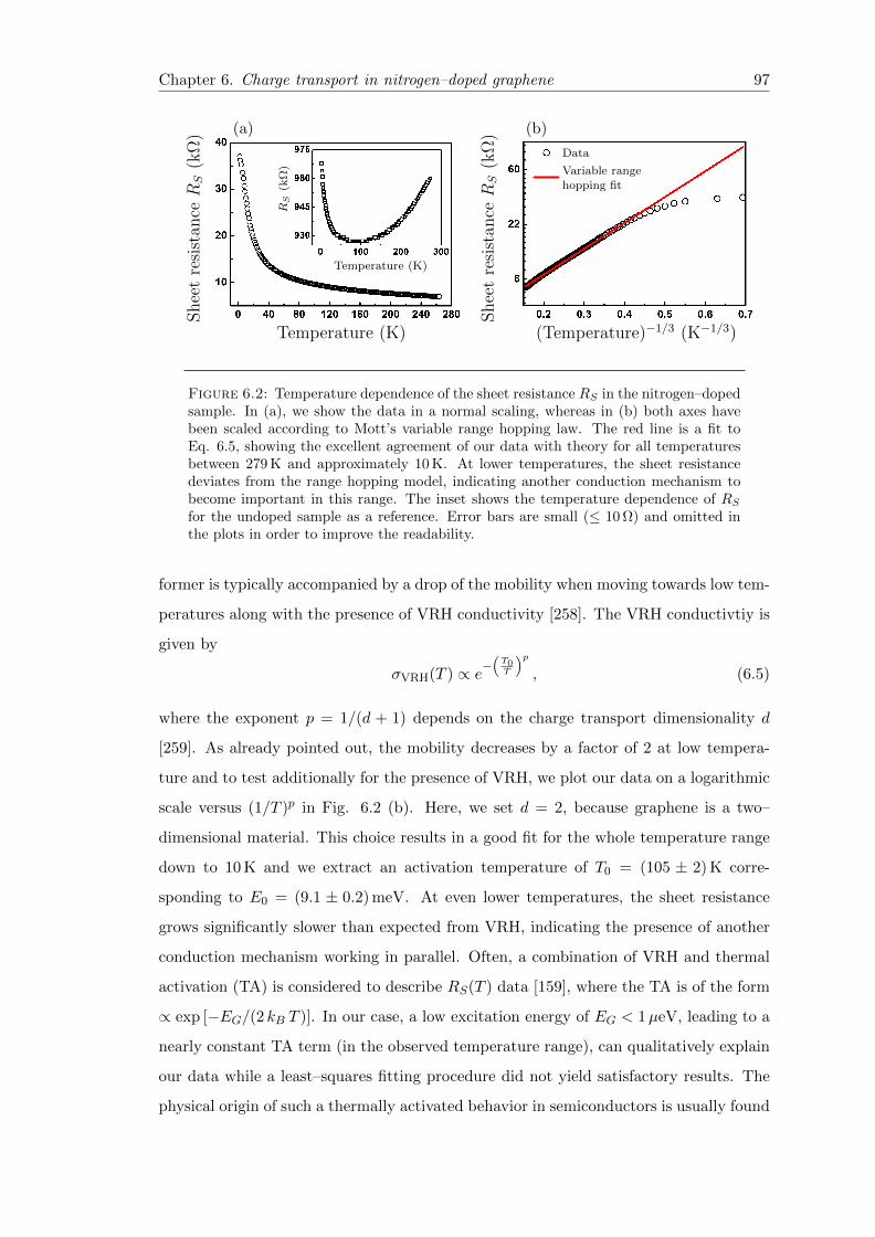
Chapter 6. Charge transport in nitrogen–doped graphene 97
(a) (b)
Shee
tre
sist
anceRS
(kΩ
)
Temperature (K)
Shee
tre
sist
anceRS
(kΩ
)
(Temperature)−1/3 (K−1/3)
RS
(kΩ
)
Temperature (K)
Data
Variable range
hopping fit
Figure 6.2: Temperature dependence of the sheet resistance RS in the nitrogen–dopedsample. In (a), we show the data in a normal scaling, whereas in (b) both axes havebeen scaled according to Mott’s variable range hopping law. The red line is a fit toEq. 6.5, showing the excellent agreement of our data with theory for all temperaturesbetween 279 K and approximately 10 K. At lower temperatures, the sheet resistancedeviates from the range hopping model, indicating another conduction mechanism tobecome important in this range. The inset shows the temperature dependence of RSfor the undoped sample as a reference. Error bars are small (≤ 10 Ω) and omitted inthe plots in order to improve the readability.
former is typically accompanied by a drop of the mobility when moving towards low tem-
peratures along with the presence of VRH conductivity [258]. The VRH conductivtiy is
given by
σVRH(T ) ∝ e−(T0T
)p, (6.5)
where the exponent p = 1/(d + 1) depends on the charge transport dimensionality d
[259]. As already pointed out, the mobility decreases by a factor of 2 at low tempera-
ture and to test additionally for the presence of VRH, we plot our data on a logarithmic
scale versus (1/T )p in Fig. 6.2 (b). Here, we set d = 2, because graphene is a two–
dimensional material. This choice results in a good fit for the whole temperature range
down to 10 K and we extract an activation temperature of T0 = (105 ± 2) K corre-
sponding to E0 = (9.1 ± 0.2) meV. At even lower temperatures, the sheet resistance
grows significantly slower than expected from VRH, indicating the presence of another
conduction mechanism working in parallel. Often, a combination of VRH and thermal
activation (TA) is considered to describe RS(T ) data [159], where the TA is of the form
∝ exp [−EG/(2 kB T )]. In our case, a low excitation energy of EG < 1µeV, leading to a
nearly constant TA term (in the observed temperature range), can qualitatively explain
our data while a least–squares fitting procedure did not yield satisfactory results. The
physical origin of such a thermally activated behavior in semiconductors is usually found
Chapter 6. Charge transport in nitrogen–doped graphene 98
in the transition of charge carriers from a valence band to a conduction band over a band
gap. In graphene, a band gap is absent and although in literature, the formation of a
gap is discussed for doped graphene [16], TA is also consistent with strongly localized
charge carriers which are excited to delocalized states in the same band [260].
6.3.3 Positive and negative magnetoresistive effects
If the behavior of RS as a function of temperature is a result of localization and disorder,
we expect to find further evidence for charge carrier localization in the magnetic field1
(B) dependence of the sheet resistance. In Fig. 6.3, we plot the magnetoresistance ratio
MR against the magnetic field, where we define
MR =RS(B)−RS(0)
RS(0)· 100 % , (6.6)
and B is applied perpendicular to the plane of current flow. At 279 K the MR increases
monotonically in the undoped graphene while at 2.5 K, the MR first decreases at low
magnetic fields (< 0.5 K) before it also starts to increase similarly to the high–T case
with a crossover to positive MR at 2.35 T. Magnetoresistance effects in graphene are
governed by different physics depending on the charge carrier density. While in the low–
density regime, the simultaneous presence of holes and electrons leads to a pronounced
MR [261], the high–density limit is metallic and transport is Drude–like. In a single–
carrier Drude model, however, no MR is expected. Nevertheless, in theories beyond
the free–electron model, the influence of non–spherical Fermi surfaces is considered and
generally, in non–magnetic conductors, the MR is a strictly positive function (f) of the
product τ B, with τ the relaxation time [245]. Since the conductivity σ is proportional
to τ one has
MR = f(σ(0)B) = f
(B
RS(0)
). (6.7)
Equation 6.7 is known as “Kohler’s rule” and for many metals it takes the form [245]
MR =
(σ(0)
2n e
)B2 · 100 % =
(µB
2
)2
· 100 % , (6.8)
1The magnetic field in the interior of our samples is not known and hence, the most concise way ofreferring to the applied magnetic field in teslas would be µ0 H, with µ0 the vacuum permeability andH the magnetic field in A/m. However, for the sake of brevity, we use the symbol B in this chapter torefer to this field.
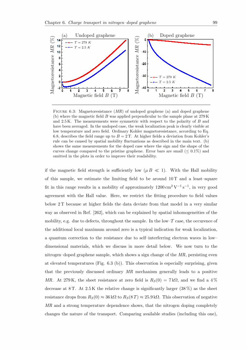
Chapter 6. Charge transport in nitrogen–doped graphene 99
(a) (b)Undoped graphene Doped graphene
Mag
net
ores
ista
nce
MR
(%)
Magnetic field B (T)
Mag
net
ores
ista
nce
MR
(%)
Magnetic field B (T)
T = 279 K
T = 2.5 K
T = 279 K
T = 2.5 K
Figure 6.3: Magnetoresistance (MR) of undoped graphene (a) and doped graphene(b) where the magnetic field B was applied perpendicular to the sample plane at 279 Kand 2.5 K. The measurements were symmetric with respect to the polarity of B andhave been averaged. In the undoped case, the weak localization peak is clearly visible atlow temperature and zero field. Ordinary Kohler magnetoresistance, according to Eq.6.8, describes the field range up to B = 2 T. At higher fields a deviation from Kohler’srule can be caused by spatial mobility fluctuations as described in the main text. (b)shows the same measurements for the doped case where the sign and the shape of thecurves change compared to the pristine graphene. Error bars are small (≤ 0.1%) andomitted in the plots in order to improve their readability.
if the magnetic field strength is sufficiently low (µB 1). With the Hall mobility
of this sample, we estimate the limiting field to be around 10 T and a least–square
fit in this range results in a mobility of approximately 1200 cm2 V−1 s−1, in very good
agreement with the Hall value. Here, we restrict the fitting procedure to field values
below 2 T because at higher fields the data deviate from that model in a very similar
way as observed in Ref. [262], which can be explained by spatial inhomogeneities of the
mobility, e.g. due to defects, throughout the sample. In the low–T case, the occurence of
the additional local maximum around zero is a typical indication for weak localization,
a quantum correction to the resistance due to self–interferring electron waves in low–
dimensional materials, which we discuss in more detail below. We now turn to the
nitrogen–doped graphene sample, which shows a sign change of the MR, persisting even
at elevated temperatures (Fig. 6.3 (b)). This observation is especially surprising, given
that the previously discussed ordinary MR mechanism generally leads to a positive
MR. At 279 K, the sheet resistance at zero field is RS(0) = 7 kΩ, and we find a 4 %
decrease at 8 T. At 2.5 K the relative change is significantly larger (38 %) as the sheet
resistance drops from RS(0) ≈ 36 kΩ to RS(8T ) ≈ 25.9 kΩ. This observation of negative
MR and a strong temperature dependence shows, that the nitrogen doping completely
changes the nature of the transport. Comparing available studies (including this one),
Chapter 6. Charge transport in nitrogen–doped graphene 100
which all observe a similar negative MR, suggests that this effect in graphene is strongly
correlated with doping together with localization and disorder [159, 263–265]. However,
the underlying mechanism is an open question. We want to attempt to understand the
negative MR by comparing our experimental data with predictions of different models.
To begin with, we consider the magnetic polaron model [264, 266]. Dopant atoms
can lead to the formation of local magnetic moments and the details of the resulting
MR depend on their interaction. We have a priori no good reasons to assume a large
interaction between such spins in our doped graphene sheet and if present, further effects
should emerge, such as a resistive hysteresis as a function of the magnetic field, which
was not observed in our measurements. However, in the case of non–interacting spins,
this model predicts an opposite temperature dependence to our experimental findings
and hence, we rule out the contribution of magnetic polarons.
Next, we consider diffusive scattering at defects [264, 267] which should be highly en-
hanced by the nitrogen atoms. The magnetic field forces the charge carriers to follow a
cyclotron trajectory with a radius rc ∝ B−1 [247]. Higher magnetic fields lead to smaller
radii and thus to less scattering at defect boundaries, which in turn decreases the resis-
tance. The magnitude of the effect will increase with decreasing temperature, just as
observed for our nitrogen-doped graphene sample. However, the theoretical calculations
predict a magnetoresistance that depends on the square of the magnetic field [267, 268],
while we observe a roughly linear dependence of the MR at higher fields for both room
temperature and low temperatures.
Finally, localization effects of charge carriers can be a the source of a negative MR,
and we have mentioned weak localization already for the undoped case. In the case of
weak localization, the largest impact is expected at low temperatures and low magnetic
fields, typically < 1 T. With no sign of saturation approaching 8 T, neither at 2.5 K, nor
at 279 K, we exclude weak localization as a main mechanism behind our experimental
results for magnetic fields above approximately 1 T. Whith no single model explaining
our observation, we now consider a superposition of different mechanisms. Following the
approach of Zhang et al. in Ref. [268], localization and diffusive boundary scattering may
result in a linear, negative MR, where the weights of this superposition are temperature
dependent. However, for the measurement at high temperature, we expect localization
effects to diminish, and as a consequence this approach does not fit to our data at 279 K.
Altogether, our observations can be explained in parts by the combined effect of different
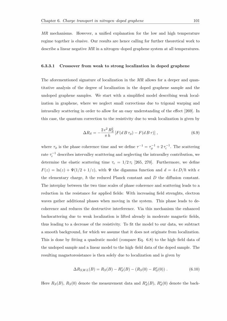
Chapter 6. Charge transport in nitrogen–doped graphene 101
MR mechanisms. However, a unified explanation for the low and high temperature
regime together is elusive. Our results are hence calling for further theoretical work to
describe a linear negative MR in a nitrogen–doped graphene system at all temperatures.
6.3.3.1 Crossover from weak to strong localization in doped graphene
The aforementioned signature of localization in the MR allows for a deeper and quan-
titative analysis of the degree of localization in the doped graphene sample and the
undoped graphene samples. We start with a simplified model describing weak local-
ization in graphene, where we neglect small corrections due to trigonal warping and
intravalley scattering in order to allow for an easy understanding of the effect [269]. In
this case, the quantum correction to the resistivity due to weak localization is given by
∆RS = −2 e2R2
S
π h[F (dB τφ)− F (dB τ)] , (6.9)
where τφ is the phase coherence time and we define τ−1 = τ−1φ + 2 τ−1
i . The scattering
rate τ−1i describes intervalley scatttering and neglecting the intravalley contribution, we
determine the elastic scattering time τe = 1/2 τi [265, 270]. Furthermore, we define
F (z) = ln(z) + Ψ(1/2 + 1/z), with Ψ the digamma function and d = 4 eD/~ with e
the elementary charge, ~ the reduced Planck constant and D the diffusion constant.
The interplay between the two time scales of phase coherence and scattering leads to a
reduction in the resistance for applied fields: With increasing field strenghts, electron
waves gather additional phases when moving in the system. This phase leads to de-
coherence and reduces the destructive interference. Via this mechanism the enhanced
backscattering due to weak localization is lifted already in moderate magnetic fields,
thus leading to a decrease of the resistivity. To fit the model to our data, we subtract
a smooth background, for which we assume that it does not originate from localization.
This is done by fitting a quadratic model (compare Eq. 6.8) to the high–field data of
the undoped sample and a linear model to the high–field data of the doped sample. The
resulting magnetoresistance is then solely due to localization and is given by
∆RS,WL(B) = RS(B)−R∗S(B)− (RS(0)−R∗S(0)) . (6.10)
Here RS(B), RS(0) denote the measurement data and R∗S(B), R∗S(0) denote the back-
Chapter 6. Charge transport in nitrogen–doped graphene 102
(a) (b)Undoped graphene Doped graphene∆RS,W
L(Ω
)
Magnetic field B (T)
∆RS,W
L(k
Ω)
Magnetic field B (T)
Data
WL fit
Data
WL fit
Figure 6.4: Background–corrected MR at low magnetic fields, originating from local-ization for the undoped sample (a) and doped sample (b). The red lines are fits of Eq.6.9.
ground resistance as described above. The results are shown in Fig. 6.4 and using the
Einstein relation for the diffusion constant D = v2F τe [270], we estimate the phase coher-
ence time and the elastic scattering time (see Tab. 6.2). In order to determine the type
and strength of the localization, we furthermore calculate the phase relaxation length
Lφ and the localization length LD based on the fit–extracted scattering times [265]:
Lφ =√D τφ , (6.11)
LD = Le exp
(σDe2/h
). (6.12)
Herein, we use the elastic scattering length Le = σD h/(2 e√π n) and the Drude con-
ductivity σD = e µn at high temperature which we calculate using the values for n and
µ derived from the Hall measurements. The values for the elastic length are both be-
low the average defect distances obtained from the Raman spectroscopy measurements
(∆L ≈ 10 nm for both samples) because the movement of electrons is influenced not only
by short range scattering centers but also by (charged) long range impurities in contrast
Sample τφ (fs) τe (fs) D (m2/s) Lφ (nm) Le (nm) LD (nm) Localization
2 164.9 ± 0.1 274 ± 9 0.274 ± 0.002 212 ± 1 29.5 ± 0.2 / weak
3 16.45 ± 0.03 130 ± 6 0.130 ± 0.001 46.2 ± 0.2 1.3 ± 0.2 10 ± 4 strong
Table 6.2: Overview of charge transport parameters in undoped graphene (sample2) and doped graphene (sample 3) as obtained from fits to the localization model (Eq.6.9) and further deduced from Eqs. 6.11, 6.12. Charge carrier scattering is drasticallyincreased and strong localization takes place in the doped case as can be inferred fromthese parameters (see main text).
Chapter 6. Charge transport in nitrogen–doped graphene 103
to the Raman D peak. The ratio of phase coherence length to localization length indi-
cates whether a system is in the weak (Lφ/LD < 1) or in the strong localization regime
(Lφ/LD > 1). If this ratio is approximately unity, a system is in the transition from
weak to strong localization. In the undoped case, the Drude conductivity is much larger
than e2/h rendering the expression in Eq. 6.12 meaningless and indicating clearly that
charge carriers are only weakly localized. In the nitrogen–doped device however, we find
an orders of magnitude change in the phase coherence time, and the scattering time,
which results in Lφ/LD ≈ 4.5. Hence the doped sample falls into the strong localization
regime. We attribute this transition from weak to strong localization to the nitrogen
defects, which form additional scattering centers and thus decrease the mean free path
of charge carriers. This quantitative result also explains the strongly reduced mobility of
the charge carriers that we measure for nitrogen-doped graphene compared to undoped
graphene and shows that we obtain a consistent picture of the effect of doping on the
charge carrier transport in graphene.
6.4 Conclusion and outlook
With our experiments, we demonstrate and quantify the significant impact of nitro-
gen doping on the graphene lattice structure as probed by Raman spectroscopy and
on the charge carrier transport properties as probed by transport measurements at
variable temperatures and magnetic fields. Samples of doped graphene and undoped
graphene were fabricated by identical CVD and transfer processes and consequently,
the charge transport measurements performed on undoped CVD–graphene are directly
comparable to the results obtained for nitrogen-doped graphene and we can trace back
the observed changes to the doping. Hall effect measurements reveal a sixfold increase
of the charge carrier density due to the doping. Furthermore, the strong temperature
dependence of the resistance is reminiscent of semiconductors, and fitting with Mott’s
variable range hopping model indicates the formation of a transport gap. A positive and
largely temperature–independent high field MR is found for undoped graphene which
we attribute to ordinary magnetoresistance mechanisms typical for metallic conduction.
In contrast, a negative MR is observed for doped graphene persisting over the whole
measured temperature range between 2.5 and 279 K and with a maximum observed
change of up to 38 % at low temperatures. While this indicates a correlation between
Chapter 6. Charge transport in nitrogen–doped graphene 104
disorder induced localization and such a large negative MR, there is no single theory,
which can consistently explain the combination of our observations for the measured
temperature and magnetic field range. Hence, our experimental findings call for fur-
ther theoretical work on the large negative MR, also at elevated temperatures. For low
temperatures and low magnetic fields, we find that fitting a weak localization model
yields excellent agreement with the measurement data. Based on the extracted phase
coherence times and elastic scattering times, we can quantify the strength of the lo-
calization by looking at the length scales of phase coherence and localization. Here,
we find the doped sample to clearly fall in the strong (Anderson) localization regime.
The deduced transport coherence times, which are directly correlated to the amount of
short– and long–ranged defect scattering centers, are reduced by orders of magnitude
in doped graphene as compared to undoped graphene. In summary, we find that the
doping consistently increases the charge carrier density, opens a transport gap, reverses
the magnetoresistance, and enhances charge carrier localization. Given the identical
fabrication processes, we can attribute all these observed effects unambiguously to the
additional dopants in the graphene, showing that nitrogen doping is a viable route for
effectively tailoring the charge transport in doped graphene. Following this path, further
exciting experiments become possible. For example, there is another approach of doping
graphene by physisorbing dopants onto the graphene surface while leaving the lattice
intact [9, 10]. This method is complementary to the substitutional doping presented
here, where carbon atoms in the crystal lattice are replace by heteroatoms. Combining
both approaches, allows for tunable and flexible transitions between n– and p–type dop-
ing in the same crystal, which demonstrates the versatility of changing the electronic
properties in graphene by controlling the degree of doping [11].
Chapter 7
Magnetic properties of chromium
trihalides
Chromium trihalides (CrX3 as introduced in Sec. 1) are layered semiconductors which
exhibit ferromagnetic coupling in each layer plane mediated by superexchange. We have
studied the three compounds CrI3, CrBr3 and CrCl3 carefully by SQUID magnetome-
try and moreover, we demonstrate that few–layer crystals can be readily obtained by
mechanical exfoliation. We find an unusual temperature dependence of the magnetiza-
tion, which we further analyze by quantifying the temperature evolution of the magne-
tocrystalline anisotropy constant Ku. In the iodide, we find it strongly changes from
Ku = (300±50) kJ/m3 at 5 K to Ku = (43±7) kJ/m3 at 60 K, close to the Curie temper-
ature. We draw a direct comparison to CrBr3, which serves as a reference, and where we
find results consistent with literature. In particular, we show that the anisotropy change
in the iodide compound is more than 3 times larger than in the bromide. A further
analysis using a classical model shows that the anisotropy constant scales with the mag-
netization at any given temperature below the Curie temperature. This scaling results
from local spin clusters having thermally induced magnetization directions that deviate
from the overall magnetization, and it indicates that the temperature dependence of the
magnetization can be explained by a dominant non–constant uniaxial anisotropy. These
results have great signficance for the understanding of the predicted magnetic coupling
in monolayer crystals of these materials. The analysis of CrI3 and CrBr3 has also been
detailed in a manuscript [21].
105
Chapter 7. Magnetic properties of chromium trihalides 106
7.1 Magnetic properties of CrX3
Magnetism in chromium trihalides arises from magnetic superexchange coupling of the
Cr3+ ions mediated via X− ions. The Goodenough–Kanamori–Anderson rules (see Sec.
2.4.3) can be applied to CrX3 systems predicting a strong ferromagnetic intralayer cou-
pling for all three compounds, CrI3, CrBr3 and CrCl3. This is suprising as it is in
contrast to many other semiconductors and insulators, where superexchange leads to
antiferromagnetism and only a few other non–metallic systems show ferromagnetism,
such as EuS, EuO, ferrites and some garnets. A detailed description of possible superex-
change paths can be found in Refs. [23, 271]. In order to apply the GKA rules correctly,
it is necessary to know the crystal structure of these trihalides. The CrX3 crystals ex-
ist in two different phases, namely in a monoclinic structure (AlCl3–type) with space
group C2/m at elevated temperatures and at lower temperatures in a trigonal structure
(BiI3–type) with space group R3. While for CrI3 and CrBr3 there is a consensus in
literature about these symmetry groups [22], there is controversy for CrCl3 [272]. In
either case, the layers extend in the ab plane and are stacked along the c axis. The
phase transition occurs at approximately 180 K for CrI3 and the two phases coexist for a
significant temperature range [22]. For CrBr3 the transition takes place at temperatures
around 420 K and for CrCl3 at around 240 K [273]. Besides the coupling of magnetic
ions within the layer planes, there is also a much weaker coupling between the layers
(see Tab. 7.1). While for CrI3 and CrBr3 the interlayer coupling is also ferromagnetic
[274], in CrCl3 it is antiferromagnetic [272, 274, 275]. In Tab. 7.1 we summarize the
magnitudes of intralayer (J) and interlayer (J ′) coupling in CrI3, CrBr3 and CrCl3.
7.2 Experimental details
The compounds CrI3, CrBr3 and CrCl3 were prepared directly from the elements in
an evacuated quartz tube using a CVD method as described in Ref. [21] resulting in
plate–like crystals that have lateral extension of millimeters while being hundreds of
micrometers thick (see Fig. 7.1).1 For the measurement of their magnetic properties
we have used a SQUID magnetometer (QuantumDesign MPMS XL).2 Samples of each
1I thank D. W. in the group of Prof. Dr. B. L. at the Max Planck Institute for Solid State Researchin Stuttgart for providing the samples.
2I thank F. R., who helped to carry out a large part of the presented measurements and who was ahelping hand in processing all measurement data.
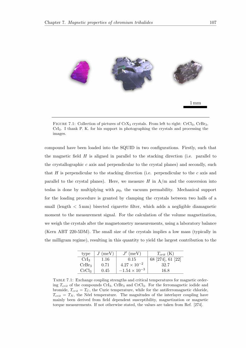
Chapter 7. Magnetic properties of chromium trihalides 107
1 mm
Figure 7.1: Collection of pictures of CrX3 crystals. From left to right: CrCl3, CrBr3,CrI3. I thank P. K. for his support in photographing the crystals and processing theimages.
compound have been loaded into the SQUID in two configurations. Firstly, such that
the magnetic field H is aligned in parallel to the stacking direction (i.e. parallel to
the crystallographic c axis and perpendicular to the crystal planes) and secondly, such
that H is perpendicular to the stacking direction (i.e. perpendicular to the c axis and
parallel to the crystal planes). Here, we measure H in A/m and the conversion into
teslas is done by multiplying with µ0, the vacuum permability. Mechanical support
for the loading procedure is granted by clamping the crystals between two halfs of a
small (length < 5 mm) bisected cigarette filter, which adds a negligible diamagnetic
moment to the measurement signal. For the calculation of the volume magnetization,
we weigh the crystals after the magnetometry measurements, using a laboratory balance
(Kern ABT 220-5DM). The small size of the crystals implies a low mass (typically in
the milligram regime), resulting in this quantity to yield the largest contribution to the
type J (meV) J ′ (meV) Tcrit (K)
CrI3 1.16 0.15 68 [274], 61 [22]CrBr3 0.71 4.27× 10⁻² 32.7CrCl3 0.45 −1.54× 10⁻³ 16.8
Table 7.1: Exchange coupling strengths and critical temperatures for magnetic order-ing Tcrit of the compounds CrI3, CrBr3 and CrCl3. For the ferromagnetic iodide andbromide, Tcrit = TC , the Curie temperature, while for the antiferromagnetic chloride,Tcrit = TN , the Neel temperature. The magnitudes of the interlayer coupling havemainly been derived from field dependent susceptibility, magnetization or magnetictorque measurements. If not otherwise stated, the values are taken from Ref. [274].
Chapter 7. Magnetic properties of chromium trihalides 108
absolute measurement error. However, the measurements of the magnetic moments of a
sample exhibit comparatively low errors due to the good signal to noise ratio, allowing
us to deduce robust conclusions for instance about the temperature dependence. Masses
and mass densities are listed in Appendix A.
7.3 Temperature dependence of the magnetization
After preparing and loading the samples into the SQUID, we measure the projection
of the magnetic moment along the (vertical) z direction at variable temperatures. In
Fig. 7.2 we present the magnetization M of all investigated compounds as a func-
tion of temperature and for the two different measurement configurations (H ‖ c and
H ⊥ c) at three different field magnitudes (0.1 T, 1 T and 5 T). Below the Curie tem-
peratures (see Tab. 7.1), we observe with further decreasing temperature an increase
of M which saturates eventually at liquid helium temperatures. When we apply a field
of 5 T, M saturates always at the same value, irrespective of whether we apply H ‖ c
or H ⊥ c. For CrI3 the saturation value is MS,5T = (206.1 ± 10.3) kA/m which cor-
responds to a magnetic moment of (3.00 ± 0.15)µB/F.U., where µB denotes the Bohr
magneton and F.U. stands for formula unit. The latter is in excellent agreement with
the expected spin–only saturation moment of Cr3+ ions µsat = g S = 3µB, where S
is the total spin quantum number and g the electron Lande factor [22]. However, for
a smaller field of 1 T, M saturates at the same value only in the H ‖ c configuration,
while in the H ⊥ c configuration, M remains at a significantly smaller saturation value
of MperpS,1 T = Mparallel
S,1 T − ∆M = (94.7 ± 3.5) kA/m. Obviously, 1 T field strength is not
sufficient to align all spins in the layer plane. Generally, such a difference ∆M can be
attributed to the effect of the magnetocrystalline anisotropy3 and here, the c axis is
found to be the easy axis. Surprisingly, for H ⊥ c there is an additional sign change
in dM/dT at approximately 53 K which cannot be explained by constant magnetocrys-
talline anisotropy and requires a more complex analysis as detailed below.
In CrBr3, the c axis is found to be the easy axis, too, while the anisotropy is clearly
smaller. For the bromide 1 T is sufficient to saturate M in both configurations at
MS,5 T = (271.1 ± 21.1) kA/m (equivalent to (3.09 ± 0.24)µB/F.U.). This saturation
value is not reached anymore when we apply magnetic fields as low as 100 mT and we
3Due to the (macroscopic) size of the crystallites, we can neglect shape anisotropy.
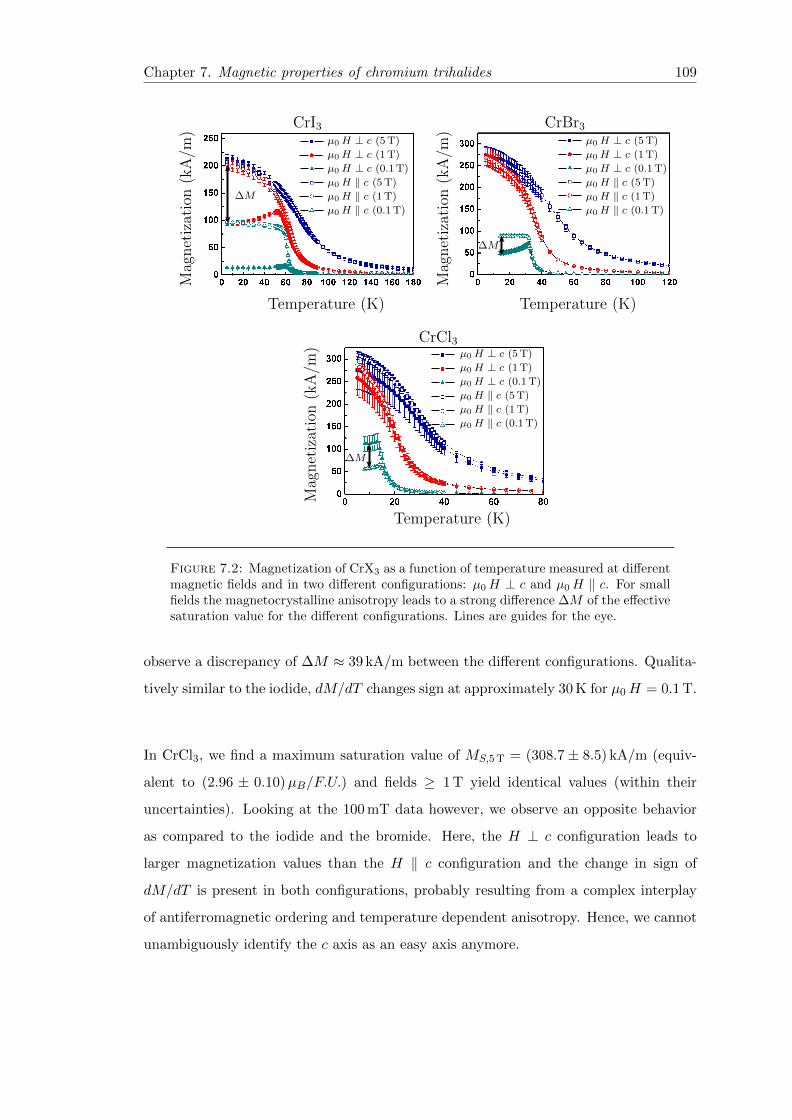
Chapter 7. Magnetic properties of chromium trihalides 109
CrI3 CrBr3
CrCl3
Temperature (K)
Temperature (K) Temperature (K)M
agnet
izat
ion
(kA
/m)
Mag
net
izat
ion
(kA
/m)
Mag
net
izat
ion
(kA
/m)
µ0H ⊥ c (5 T)
µ0H ⊥ c (1 T)
µ0H ⊥ c (0.1 T)
µ0H ‖ c (5 T)
µ0H ‖ c (1 T)
µ0H ‖ c (0.1 T)
µ0H ⊥ c (5 T)
µ0H ⊥ c (1 T)
µ0H ⊥ c (0.1 T)
µ0H ‖ c (5 T)
µ0H ‖ c (1 T)
µ0H ‖ c (0.1 T)
µ0H ⊥ c (5 T)
µ0H ⊥ c (1 T)
µ0H ⊥ c (0.1 T)
µ0H ‖ c (5 T)
µ0H ‖ c (1 T)
µ0H ‖ c (0.1 T)
∆M
∆M
∆M
Figure 7.2: Magnetization of CrX3 as a function of temperature measured at differentmagnetic fields and in two different configurations: µ0H ⊥ c and µ0H ‖ c. For smallfields the magnetocrystalline anisotropy leads to a strong difference ∆M of the effectivesaturation value for the different configurations. Lines are guides for the eye.
observe a discrepancy of ∆M ≈ 39 kA/m between the different configurations. Qualita-
tively similar to the iodide, dM/dT changes sign at approximately 30 K for µ0H = 0.1 T.
In CrCl3, we find a maximum saturation value of MS,5 T = (308.7 ± 8.5) kA/m (equiv-
alent to (2.96 ± 0.10)µB/F.U.) and fields ≥ 1 T yield identical values (within their
uncertainties). Looking at the 100 mT data however, we observe an opposite behavior
as compared to the iodide and the bromide. Here, the H ⊥ c configuration leads to
larger magnetization values than the H ‖ c configuration and the change in sign of
dM/dT is present in both configurations, probably resulting from a complex interplay
of antiferromagnetic ordering and temperature dependent anisotropy. Hence, we cannot
unambiguously identify the c axis as an easy axis anymore.
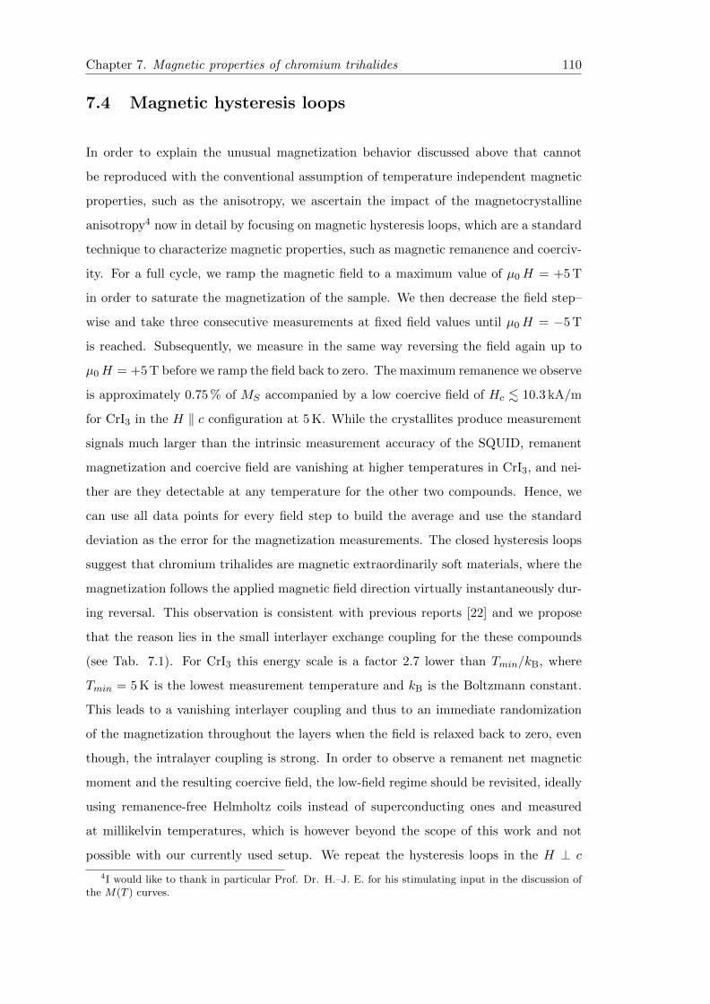
Chapter 7. Magnetic properties of chromium trihalides 110
7.4 Magnetic hysteresis loops
In order to explain the unusual magnetization behavior discussed above that cannot
be reproduced with the conventional assumption of temperature independent magnetic
properties, such as the anisotropy, we ascertain the impact of the magnetocrystalline
anisotropy4 now in detail by focusing on magnetic hysteresis loops, which are a standard
technique to characterize magnetic properties, such as magnetic remanence and coerciv-
ity. For a full cycle, we ramp the magnetic field to a maximum value of µ0H = +5 T
in order to saturate the magnetization of the sample. We then decrease the field step–
wise and take three consecutive measurements at fixed field values until µ0H = −5 T
is reached. Subsequently, we measure in the same way reversing the field again up to
µ0H = +5 T before we ramp the field back to zero. The maximum remanence we observe
is approximately 0.75 % of MS accompanied by a low coercive field of Hc . 10.3 kA/m
for CrI3 in the H ‖ c configuration at 5 K. While the crystallites produce measurement
signals much larger than the intrinsic measurement accuracy of the SQUID, remanent
magnetization and coercive field are vanishing at higher temperatures in CrI3, and nei-
ther are they detectable at any temperature for the other two compounds. Hence, we
can use all data points for every field step to build the average and use the standard
deviation as the error for the magnetization measurements. The closed hysteresis loops
suggest that chromium trihalides are magnetic extraordinarily soft materials, where the
magnetization follows the applied magnetic field direction virtually instantaneously dur-
ing reversal. This observation is consistent with previous reports [22] and we propose
that the reason lies in the small interlayer exchange coupling for the these compounds
(see Tab. 7.1). For CrI3 this energy scale is a factor 2.7 lower than Tmin/kB, where
Tmin = 5 K is the lowest measurement temperature and kB is the Boltzmann constant.
This leads to a vanishing interlayer coupling and thus to an immediate randomization
of the magnetization throughout the layers when the field is relaxed back to zero, even
though, the intralayer coupling is strong. In order to observe a remanent net magnetic
moment and the resulting coercive field, the low-field regime should be revisited, ideally
using remanence-free Helmholtz coils instead of superconducting ones and measured
at millikelvin temperatures, which is however beyond the scope of this work and not
possible with our currently used setup. We repeat the hysteresis loops in the H ⊥ c
4I would like to thank in particular Prof. Dr. H.–J. E. for his stimulating input in the discussion ofthe M(T ) curves.
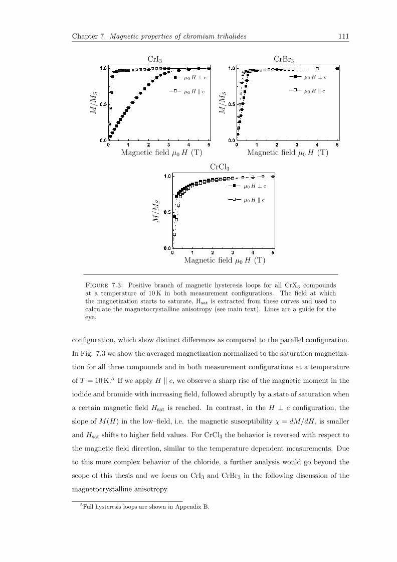
Chapter 7. Magnetic properties of chromium trihalides 111
CrI3 CrBr3
CrCl3
Magnetic field µ0H (T)
Magnetic field µ0H (T) Magnetic field µ0H (T)M/M
S
M/M
S
M/M
S
µ0 H ⊥ c
µ0 H ‖ c
µ0 H ⊥ c
µ0 H ‖ c
µ0 H ⊥ c
µ0 H ‖ c
Figure 7.3: Positive branch of magnetic hysteresis loops for all CrX3 compoundsat a temperature of 10 K in both measurement configurations. The field at whichthe magnetization starts to saturate, Hsat is extracted from these curves and used tocalculate the magnetocrystalline anisotropy (see main text). Lines are a guide for theeye.
configuration, which show distinct differences as compared to the parallel configuration.
In Fig. 7.3 we show the averaged magnetization normalized to the saturation magnetiza-
tion for all three compounds and in both measurement configurations at a temperature
of T = 10 K.5 If we apply H ‖ c, we observe a sharp rise of the magnetic moment in the
iodide and bromide with increasing field, followed abruptly by a state of saturation when
a certain magnetic field Hsat is reached. In contrast, in the H ⊥ c configuration, the
slope of M(H) in the low–field, i.e. the magnetic susceptibility χ = dM/dH, is smaller
and Hsat shifts to higher field values. For CrCl3 the behavior is reversed with respect to
the magnetic field direction, similar to the temperature dependent measurements. Due
to this more complex behavior of the chloride, a further analysis would go beyond the
scope of this thesis and we focus on CrI3 and CrBr3 in the following discussion of the
magnetocrystalline anisotropy.
5Full hysteresis loops are shown in Appendix B.
Chapter 7. Magnetic properties of chromium trihalides 112
7.5 Magnetic anisotropy in CrI3 and CrBr3
The saturation field Hsat, which can be observed in the measurements in the H ⊥ c
configuration is a direct measure of the magnetocrystalline anisotropy. The magne-
tocrystalline anisotropy contributes to the micromagnetic energy density with a term
EA = Ku sin2 (θ − φ) (7.1)
In this formula, Ku denotes the uniaxial anisotropy constant, θ the direction of the
preferred magnetization and φ the direction in which the magnetization points. If we
consider the sample being fully magnetized aboveHsat, the single domain state becomes a
valid approximation for CrI3 and CrBr3, which can be described by the Stoner–Wohlfarth
model [276]. Within this model, the anisotropy constant can be derived via
2Ku
MS= µ0Hsat . (7.2)
We extract Hsat from the hysteresis loops by determining the point of maximal curva-
ture of the hysteresis curve directly below the region of saturation. In order to obtain
the acurate value for the saturation magnetization, we correct for a small paramag-
netic contribution in the saturation region by subtracting the slope of a linear fit in
the field intervals |H| > |Hsat|. Measuring hysteresis loops for various temperatures
allows us then to deduce the anisotropy constant as a function of temperature for both
compounds, CrI3 and CrBr3, as shown in Fig. 7.4. The temperature dependence of
CrBr3’s anisotropy has been reported in the early stages of CrX3 research by Dillon
[24, 277] and in Fig. 7.4 (b), we plot our measurement together with the temperature
dependence extracted from Ref. [24]. For the whole temperature range, we find an excel-
lent agreement, corroborating the validity of using Eq. 7.2, where the low–temperature
anisotropy amounts to Ku = (86.1± 6.0) kJ/m3. For CrI3 on the other hand, this is to
the best of our knowledge the first determination of a temperature dependence in Ku.
As in CrBr3, the anisotropy decreases towards TC . At 5 K, the experimental value is
Ku = (301 ± 50) kJ/m3. We now compare this with numerical calculations of the CrI3
system based on density functional theory.6 The details of the calculation are described
6I thank Dr. N. S. in the group of Prof. Dr. U. S. at the Materials Science and Engineering andPhysical Sciences and Engineering Division of the King Abdullah University of Science and Technology(KAUST) in Thuwal for providing these calculations.
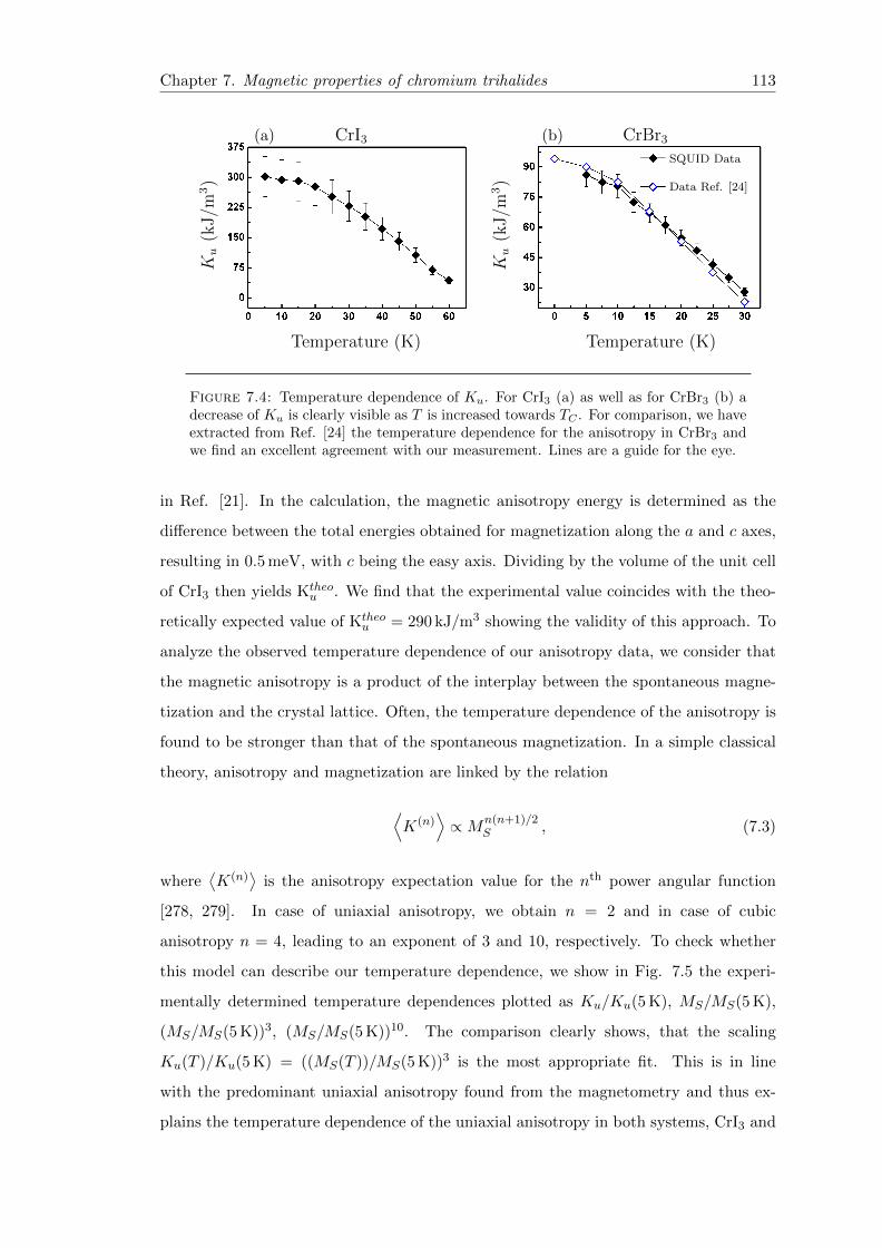
Chapter 7. Magnetic properties of chromium trihalides 113
(a) CrI3 (b) CrBr3
Temperature (K) Temperature (K)
Ku
(kJ/m
3)
Ku
(kJ/m
3)
SQUID Data
Data Ref. [24]
Figure 7.4: Temperature dependence of Ku. For CrI3 (a) as well as for CrBr3 (b) adecrease of Ku is clearly visible as T is increased towards TC . For comparison, we haveextracted from Ref. [24] the temperature dependence for the anisotropy in CrBr3 andwe find an excellent agreement with our measurement. Lines are a guide for the eye.
in Ref. [21]. In the calculation, the magnetic anisotropy energy is determined as the
difference between the total energies obtained for magnetization along the a and c axes,
resulting in 0.5 meV, with c being the easy axis. Dividing by the volume of the unit cell
of CrI3 then yields Ktheou . We find that the experimental value coincides with the theo-
retically expected value of Ktheou = 290 kJ/m3 showing the validity of this approach. To
analyze the observed temperature dependence of our anisotropy data, we consider that
the magnetic anisotropy is a product of the interplay between the spontaneous magne-
tization and the crystal lattice. Often, the temperature dependence of the anisotropy is
found to be stronger than that of the spontaneous magnetization. In a simple classical
theory, anisotropy and magnetization are linked by the relation
⟨K(n)
⟩∝Mn(n+1)/2
S , (7.3)
where⟨K(n)
⟩is the anisotropy expectation value for the nth power angular function
[278, 279]. In case of uniaxial anisotropy, we obtain n = 2 and in case of cubic
anisotropy n = 4, leading to an exponent of 3 and 10, respectively. To check whether
this model can describe our temperature dependence, we show in Fig. 7.5 the experi-
mentally determined temperature dependences plotted as Ku/Ku(5 K), MS/MS(5 K),
(MS/MS(5 K))3, (MS/MS(5 K))10. The comparison clearly shows, that the scaling
Ku(T )/Ku(5 K) = ((MS(T ))/MS(5 K))3 is the most appropriate fit. This is in line
with the predominant uniaxial anisotropy found from the magnetometry and thus ex-
plains the temperature dependence of the uniaxial anisotropy in both systems, CrI3 and
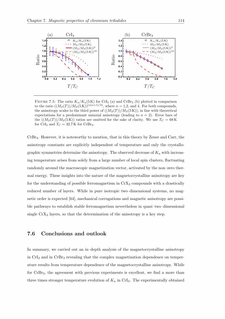
Chapter 7. Magnetic properties of chromium trihalides 114
(a) (b)CrI3 CrBr3
T/TC T/TC
Rat
io
Rat
io
Ku/Ku(5 K)
MS/MS(5 K)
(MS/MS(5 K))3
(MS/MS(5 K))10
Ku/Ku(5 K)
MS/MS(5 K)
(MS/MS(5 K))3
(MS/MS(5 K))10
Figure 7.5: The ratio Ku/Ku(5 K) for CrI3 (a) and CrBr3 (b) plotted in comparisonto the ratio ((MS(T ))/MS(5 K))(n(n+1)/2), where n = 1,2, and 4. For both compounds,the anisotropy scales to the third power of ((MS(T ))/MS(5 K)), in line with theoreticalexpectations for a predominant uniaxial anisotropy (leading to n = 2). Error bars ofthe ((MS(T ))/MS(5 K)) ratios are omitted for the sake of clarity. We use TC = 68 Kfor CrI3 and TC = 32.7 K for CrBr3.
CrBr3. However, it is noteworthy to mention, that in this theory by Zener and Carr, the
anisotropy constants are explicitly independent of temperature and only the crystallo-
graphic symmetries determine the anisotropy. The observed decrease of Ku with increas-
ing temperature arises from solely from a large number of local spin clusters, fluctuating
randomly around the macroscopic magnetization vector, activated by the non–zero ther-
mal energy. These insights into the nature of the magnetocrystalline anisotropy are key
for the understanding of possible ferromagnetism in CrX3 compounds with a drastically
reduced number of layers. While in pure isotropic two–dimensional systems, no mag-
netic order is expected [64], mechanical corrugations and magnetic anisotropy are possi-
ble pathways to establish stable ferromagnetism nevertheless in quasi–two–dimensional
single CrX3 layers, so that the determination of the anisotropy is a key step.
7.6 Conclusions and outlook
In summary, we carried out an in–depth analysis of the magnetocrystalline anisotropy
in CrI3 and in CrBr3 revealing that the complex magnetization dependence on temper-
ature results from temperature dependence of the magnetocrystalline anisotropy. While
for CrBr3, the agreement with previous experiments is excellent, we find a more than
three times stronger temperature evolution of Ku in CrI3. The experimentally obtained
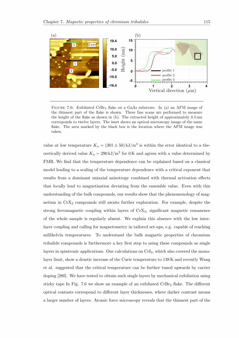
Chapter 7. Magnetic properties of chromium trihalides 115
-16.4 0 1 2 3 4
-5
0
5
10
15
-10.0
-5.0
0.0
5.0
10.0
19.4
(a) (b)
Vertical direction (µm)
Hei
ght
(nm
)
profile 1
profile 2
profile 3
1
2
3 2µm
Figure 7.6: Exfoliated CrBr3 flake on a GaAs substrate. In (a) an AFM image ofthe thinnest part of the flake is shown. Three line scans are performed to measurethe height of the flake as shown in (b). The extracted height of approximately 8.5 nmcorresponds to twelve layers. The inset shows an optical microscopy image of the sameflake. The area marked by the black box is the location where the AFM image wastaken.
value at low temperature Ku = (301± 50) kJ/m3 is within the error identical to a the-
oretically derived value Ku = 290 kJ/m3 for 0 K and agrees with a value determined by
FMR. We find that the temperature dependence can be explained based on a classical
model leading to a scaling of the temperature dependence with a critical exponent that
results from a dominant uniaxial anisotropy combined with thermal activation effects
that locally lead to magnetization deviating from the ensemble value. Even with this
understanding of the bulk compounds, our results show that the phenomenology of mag-
netism in CrX3 compounds still awaits further exploration. For example, despite the
strong ferromagnetic coupling within layers of CrX3, significant magnetic remanence
of the whole sample is regularly absent. We explain this absence with the low inter-
layer coupling and calling for magnetometry in tailored set-ups, e.g. capable of reaching
millikelvin temperatures. To understand the bulk magnetic properties of chromium
trihalide compounds is furthermore a key first step to using these compounds as single
layers in spintronic applications. Our calculations on CrI3, which also covered the mono-
layer limit, show a drastic increase of the Curie temperature to 138 K and recently Wang
et al. suggested that the critical temperature can be further tuned upwards by carrier
doping [280]. We have tested to obtain such single layers by mechanical exfoliation using
sticky tape In Fig. 7.6 we show an example of an exfoliated CrBr3 flake. The different
optical contasts correspond to different layer thicknesses, where darker contrast means
a larger number of layers. Atomic force microscopy reveals that the thinnest part of the
Chapter 7. Magnetic properties of chromium trihalides 116
flake has a thickness of approximately (8.5±0.5) nm which corresponds to twelve layers.
Finally, the experiments show, that most of the obtained crystals are not stable under
ambient atmosphere, with a possible degradation mechanism according to the reaction:
CrX3 + xH2O → CrX3 · xH2O. An illustration of this degradation process in CrBr3
can be found in the Appendix B. While we have found CrCl3 to be the most stable
compound, we suggest to conduct the exfoliation procedure of the other two compounds
under inert gas atmosphere and use encapsulation techniques, e.g. with hexagonal boron
nitride similar to encapsulation of graphene layers [281]. Only then, this exciting mate-
rials class will be able to show its full potential for ultra–thin spintronics.
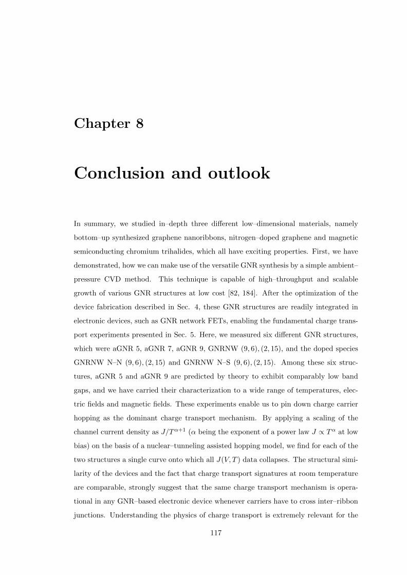
Chapter 8
Conclusion and outlook
In summary, we studied in–depth three different low–dimensional materials, namely
bottom–up synthesized graphene nanoribbons, nitrogen–doped graphene and magnetic
semiconducting chromium trihalides, which all have exciting properties. First, we have
demonstrated, how we can make use of the versatile GNR synthesis by a simple ambient–
pressure CVD method. This technique is capable of high–throughput and scalable
growth of various GNR structures at low cost [82, 184]. After the optimization of the
device fabrication described in Sec. 4, these GNR structures are readily integrated in
electronic devices, such as GNR network FETs, enabling the fundamental charge trans-
port experiments presented in Sec. 5. Here, we measured six different GNR structures,
which were aGNR 5, aGNR 7, aGNR 9, GNRNW (9, 6), (2, 15), and the doped species
GNRNW N–N (9, 6), (2, 15) and GNRNW N–S (9, 6), (2, 15). Among these six struc-
tures, aGNR 5 and aGNR 9 are predicted by theory to exhibit comparably low band
gaps, and we have carried their characterization to a wide range of temperatures, elec-
tric fields and magnetic fields. These experiments enable us to pin down charge carrier
hopping as the dominant charge transport mechanism. By applying a scaling of the
channel current density as J/Tα+1 (α being the exponent of a power law J ∝ Tα at low
bias) on the basis of a nuclear–tunneling assisted hopping model, we find for each of the
two structures a single curve onto which all J(V, T ) data collapses. The structural simi-
larity of the devices and the fact that charge transport signatures at room temperature
are comparable, strongly suggest that the same charge transport mechanism is opera-
tional in any GNR–based electronic device whenever carriers have to cross inter–ribbon
junctions. Understanding the physics of charge transport is extremely relevant for the
117
Chapter 8. Conclusion and outlook 118
Material µ (cm2 V−1 s−1) n (cm−2) ∆ (eV) Conduction mechanism
aGNR 5 0.01 [*] ≥ 1012 [*] 1.7 [6] hopping [*]
aGNR 7 10−5 [*] n/a 3.8 [6] hopping [*]
aGNR 9 10−4 – 10−3 [*] ≥ 1011 [*] 2.1 [6]hopping [*]
tunneling [222]
GNRNW (9, 6), (2, 15) 10−4 [*] n/a 1.6 [79] hopping [*]
SLG ≥ 103 [*] ≥ 1012 [*] 0 [29] band–like [*]
SLG encapsulated ≥ 105 [160] ≥ 1011 [160] 0 [29] band–like [160]
Doped SLG ≥ 101 ≥ 1013 [*] ≈ 0.09 [*] hopping [*] and [159]
Epitaxial graphene ≈ 104 [282] ≥ 1012 [282] 0 [187] band–like [282]
TG ≥ 104 [147] ≈ 1011 [147] 0 [187] band–like [147]
Table 8.1: Overview of electronic properties of various graphene materials. Themobilities are extracted from gate dependent transport measurements and Hall mea-surements. Charge carrier densities in unprotected devices are typically dominatedby extrinsic doping. The transport gaps for the GNRs, (encapsulated) SLG, epitaxialgraphene and TG are theoretically expected band gaps. The transport gap of dopedgraphene is the one determined in Sec. 6 and in this system mobility and charge car-rier density stronlgy depend on the doping level. Note that there is a large varietyin epitaxial graphene, depending on the growth conditions and number of layers. Thevalues marked by [*] are from this work. This overview and references herein are notexhaustive.
interpretation of any experiment dealing with GNR–based devices and for the future
development of GNR–based electronics. In order to give an overview of key parameters
of charge transport, we summarize state–of–the–art values for charge carrier mobility
µ, charge carrier density n, transport gap (e.g. band gap) ∆ and the dominant charge
transport mechanism for various graphene materials in Tab. 8.1. Here, we can see that
hopping transport is regularly accompanied by low values of µ, and large mobilites are
only possible in protected SLG and TG systems with delocalized electron transport.
Therefore, based on our results, we understand the disparity of mobilities measured in
lateral transport experiments (this work) compared to mobilities estimated from ter-
ahertz spectroscopy, which are in the order of 102 cm2 V−1 s−1 for aGNR 9 samples
[184]. The performances of FET devices fabricated are limited by inter–ribbon hopping
processes, limiting the possible intrinsic transport properties of the single GNRs. De-
spite the advances in the understanding of bottom–up GNR–based electronic devices,
where we contribute with this work by elucidating the charge transport mechanism in
Chapter 8. Conclusion and outlook 119
an important class of such devices, we see that this field is still in its early stages. In
particular, the growth of longer GNRs through optimization of the CVD process will
enable the engineering of electrical contacts for single crystalline GNR units. This is
an important prerequisite to reach the realm of delocalized band transport. Together
with the development of wider GNRs with smaller band gaps, the availability of band
transport dominated devices will be key for a possible use of GNRs in future electron-
ics. Up to now, the band gaps of the bottom–up GNRs used for device studies are
several hundred millielectronvolts above the technologically relevant silicon band gap of
approximately 1.1 eV [31]. In parallel, we started to explore graphitic electrodes (see
Sec. 4.3.3), where carbon–carbon interactions improve the electrical contact, which will
also facilitate transport experiments on chemically derived GNRs. Finally, extended re-
search on SLG showed that encapsulation and atomically flat substrates (e.g. hexagonal
boron nitride) [160] will eventually be required to maximize device performance of such
sensitive low–dimensional systems. Following these routes, GNRs may provide practi-
cal solutions to the current challenges for nano–electronic, optoelectronic, and photonic
devices in the future.
In Sec. 6, we demonstrated that substitutional doping of graphene, e.g. by nitrogen,
is an alternative pathway towards low–dimensional materials with tailor–made charge
transport properties. In our experiments, we find that increasing the level of N-doping
leads to a gradual change in the shape of the magnetoresistance accompanied with
a sign change from positive to negative magnetoresistance. Further studies combining
structural and electrical investigation will complete the picture of the electronic structure
changing with the configuration and arrangement of the nitrogen dopants in graphene.
As an example, it has been shown that photochemical doping allows one to tune the
Fermi level of graphene locally with complex and controllable spatial doping profiles
opening the way for novel applications such as optically defined p–n–junctions [11].
Lastly, we investigated pathways towards monolayer materials with ferromagnetic order
in Sec. 7. Ferromagnetic monolayers of CrI3 have been demonstrated only recently [20].
In this work, we focussed in particular on the magnetic anisotropy of CrI3 and CrBr3
tackling a key open question, which is the stabilization of ferroic order in these layered
two dimensional systems. The magnetocrystalline anisotropy is a possible ingredient that
can allow one to overcome the limitations set by the Mermin-Wagner theorem [64], which
prohibits magnetic ordering in two or less dimensions. In this work, we find for CrI3 that
Chapter 8. Conclusion and outlook 120
the magnetocrystalline anisotropy constant strongly changes fromKu = (300±50) kJ/m3
at 5 K to Ku = (43 ± 7) kJ/m3 at 60 K, close to the Curie temperature and compare
this change with the temperature evolution of Ku in CrBr3. Our analysis shows that
the temperature dependence of the magnetization in these compounds can be explained
by a dominant uniaxial anisotropy. Additionally, theoretical calculations show not only
qualitative, but even quantitative agreement. Therefore, we find the anisotropy to be
a key aspect to understanding the magnetism in this class of materials paving the way
towards the exploration of unexpected and new phenomena such as spin–filtered light
emitting diodes [28].

Appendix A
Additional material for Chapter 4
121
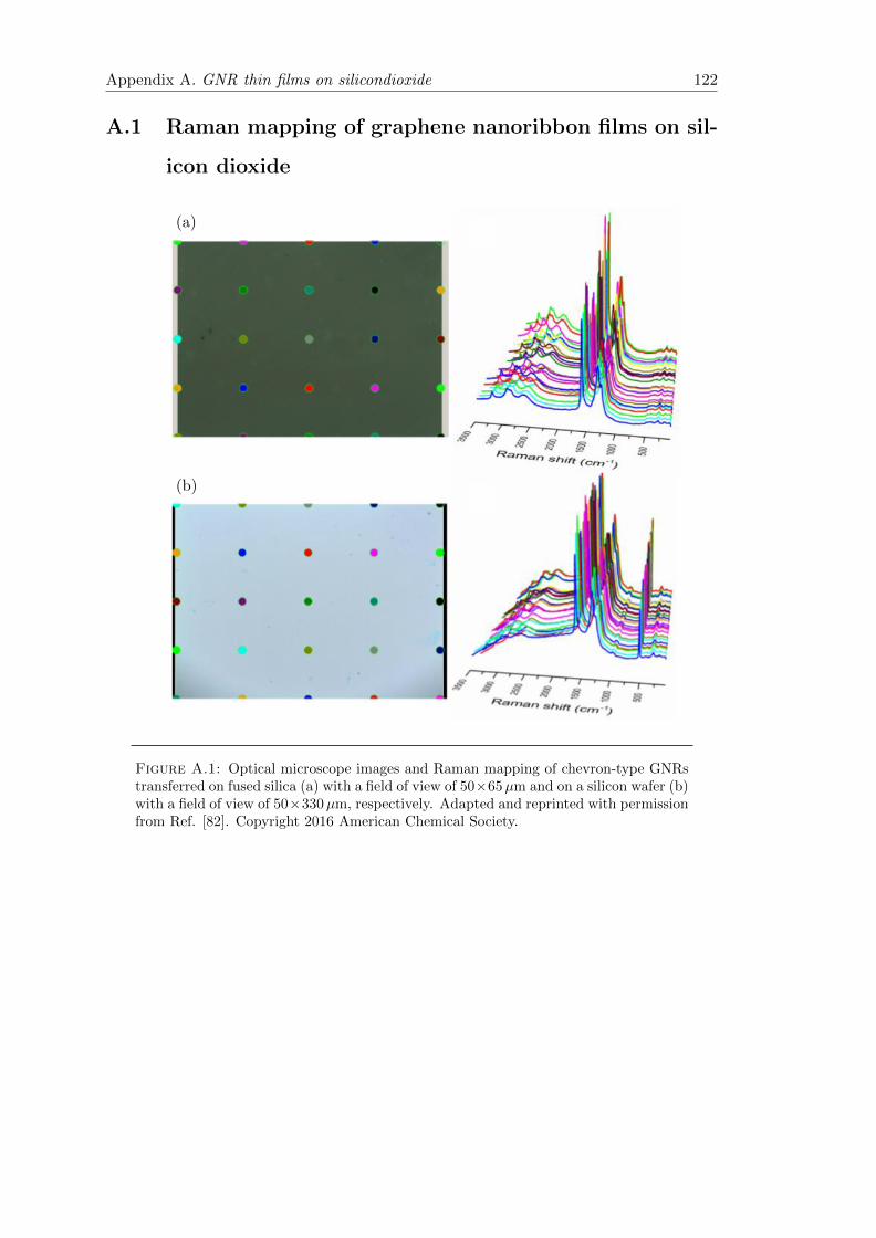
Appendix A. GNR thin films on silicondioxide 122
A.1 Raman mapping of graphene nanoribbon films on sil-
icon dioxide
(a)
(b)
Figure A.1: Optical microscope images and Raman mapping of chevron-type GNRstransferred on fused silica (a) with a field of view of 50×65µm and on a silicon wafer (b)with a field of view of 50×330µm, respectively. Adapted and reprinted with permissionfrom Ref. [82]. Copyright 2016 American Chemical Society.
Appendix B
Additional material for Chapter 5
123
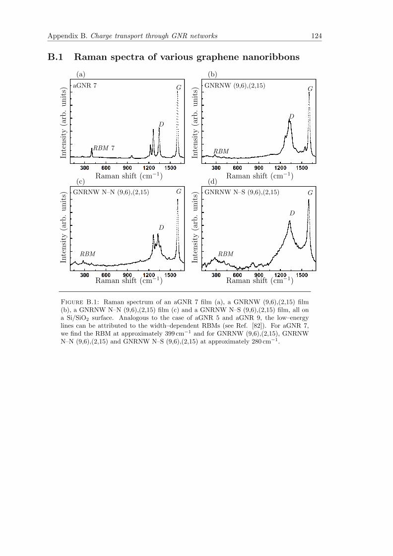
Appendix B. Charge transport through GNR networks 124
B.1 Raman spectra of various graphene nanoribbons
(a)
aGNR 7
Inte
nsi
ty(a
rb.
unit
s)
Raman shift (cm−1)
RBM 7
D
G
(b)
GNRNW (9,6),(2,15)
Inte
nsi
ty(a
rb.
unit
s)
Raman shift (cm−1)
RBM
D
G
(c)
GNRNW N–N (9,6),(2,15)
Inte
nsi
ty(a
rb.
unit
s)
Raman shift (cm−1)
RBM
D
G
(d)
GNRNW N–S (9,6),(2,15)In
tensi
ty(a
rb.
unit
s)
Raman shift (cm−1)
RBM
D
G
Figure B.1: Raman spectrum of an aGNR 7 film (a), a GNRNW (9,6),(2,15) film(b), a GNRNW N–N (9,6),(2,15) film (c) and a GNRNW N–S (9,6),(2,15) film, all ona Si/SiO2 surface. Analogous to the case of aGNR 5 and aGNR 9, the low–energylines can be attributed to the width–dependent RBMs (see Ref. [82]). For aGNR 7,we find the RBM at approximately 399 cm−1 and for GNRNW (9,6),(2,15), GNRNWN–N (9,6),(2,15) and GNRNW N–S (9,6),(2,15) at approximately 280 cm−1.
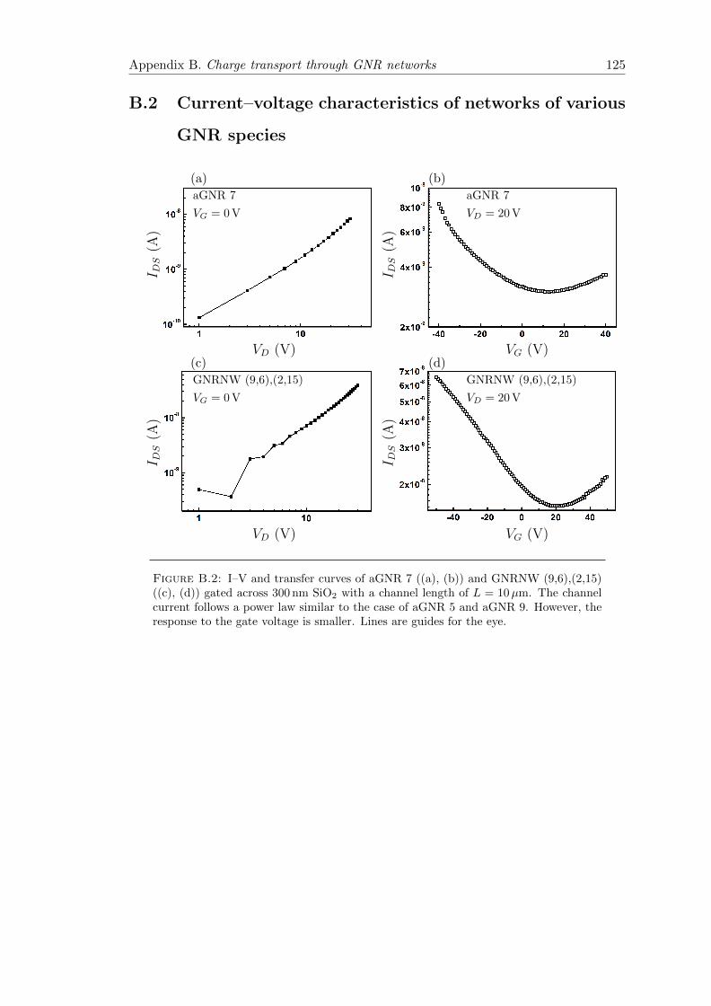
Appendix B. Charge transport through GNR networks 125
B.2 Current–voltage characteristics of networks of various
GNR species
(a)
aGNR 7
I DS
(A)
VD (V)
VG = 0 V
(b)
aGNR 7
I DS
(A)
VG (V)
VD = 20 V
(c)
GNRNW (9,6),(2,15)
I DS
(A)
VD (V)
VG = 0 V
(d)
GNRNW (9,6),(2,15)I D
S(A
)
VG (V)
VD = 20 V
Figure B.2: I–V and transfer curves of aGNR 7 ((a), (b)) and GNRNW (9,6),(2,15)((c), (d)) gated across 300 nm SiO2 with a channel length of L = 10µm. The channelcurrent follows a power law similar to the case of aGNR 5 and aGNR 9. However, theresponse to the gate voltage is smaller. Lines are guides for the eye.
...
...
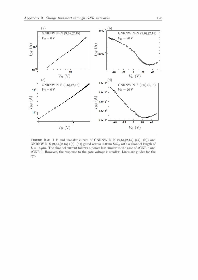
Appendix B. Charge transport through GNR networks 126
(a)
GNRNW N–N (9,6),(2,15)I D
S(A
)
VD (V)
VG = 0 V
(b)
GNRNW N–N (9,6),(2,15)
I DS
(A)
VG (V)
VD = 20 V
(c)
GNRNW N–S (9,6),(2,15)
I DS
(A)
VD (V)
VG = 0 V
(d)
GNRNW N–S (9,6),(2,15)
I DS
(A)
VG (V)
VD = 20 V
Figure B.3: I–V and transfer curves of GNRNW N–N (9,6),(2,15) ((a), (b)) andGNRNW N–S (9,6),(2,15) ((c), (d)) gated across 300 nm SiO2 with a channel length ofL = 15µm. The channel current follows a power law similar to the case of aGNR 5 andaGNR 9. However, the response to the gate voltage is smaller. Lines are guides for theeye.
...
...
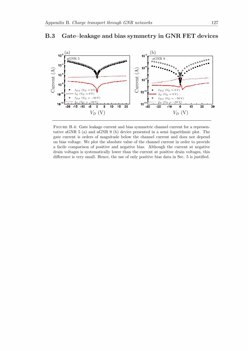
Appendix B. Charge transport through GNR networks 127
B.3 Gate–leakage and bias symmetry in GNR FET devices
(a)
VD (V)
Curr
ent
(A)
aGNR 5
IDS (VG = 0 V)
IG (VG = 0 V)
IDS (VG = −50 V)
IG (VG = −50 V)
(b)
VD (V)
Curr
ent
(A)
aGNR 9
IDS (VG = 0 V)
IG (VG = 0 V)
IDS (VG = −50 V)
IG (VG = −50 V)
Figure B.4: Gate leakage current and bias symmetric channel current for a represen-tative aGNR 5 (a) and aGNR 9 (b) device presented in a semi–logarithmic plot. Thegate current is orders of magnitude below the channel current and does not dependon bias voltage. We plot the absolute value of the channel current in order to providea facile comparison of positive and negative bias. Although the current at negativedrain voltages is systematically lower than the current at positive drain voltages, thisdifference is very small. Hence, the use of only positive bias data in Sec. 5 is justified.
...
Appendix B. Charge transport through GNR networks 128
B.4 Determination of the field–effect mobility in GNR net-
work FETs
The field–effect mobility can generally be extracted from the transfer curve according
to Ref. [226] via
µFE =g
VD COx
L
W, (B.1)
where g = ∂ISD∂VG
is the transconductance, L is the channel length, W is the channel width
and COx = ε ε0/tOx ≈ 1.15×10⁻⁴ F/m2 is the geometrical capacitance density assuming
that the channel and the gate electrode form a parallel plate capacitor. Here, we use
tOx = 300 nm, the relative permittivity of SiO2 ε = 3.9 and the vacuum permittivity
ε0 ≈ 8.854 F/m. Ideally, the transconductance is determined in the linear regime of the
transfer curve. However, with the GNR network FET devices investigated in Sec. 5 a
linear regime is not reached. Therefore, we use a linear approximation of the curve in the
range VG ≤ −40 V. In the linear regime of transfer curves, the channel current is usually
much larger than in the subthreshold regime and therefore the transconductance which
we extract in this way leads to a systematic underestimation of µFE. Hence, the values
given for µFE in Sec. 5 are estimates. However, the contact resistance–free mobilities
as determined in Sec. 5.2.3 are of the same magnitude showing that the systematic
error in the field–effect mobility is small and hence these values represent a realistic
approximation of the charge carrier mobility in the devices. Furthermore, we use µFE in
Sec. B.6 for the calculation of the charge carrier density as a function of temperature.
The systematic error in the mobility of course propagates to the charge carrier density.
Nevertheless, the temperature dependence of the transfer curves is captured correctly
in the field–effect mobility and therefore the statements in Secs. 5 and B.6 are robust
against these systematic uncertainties.
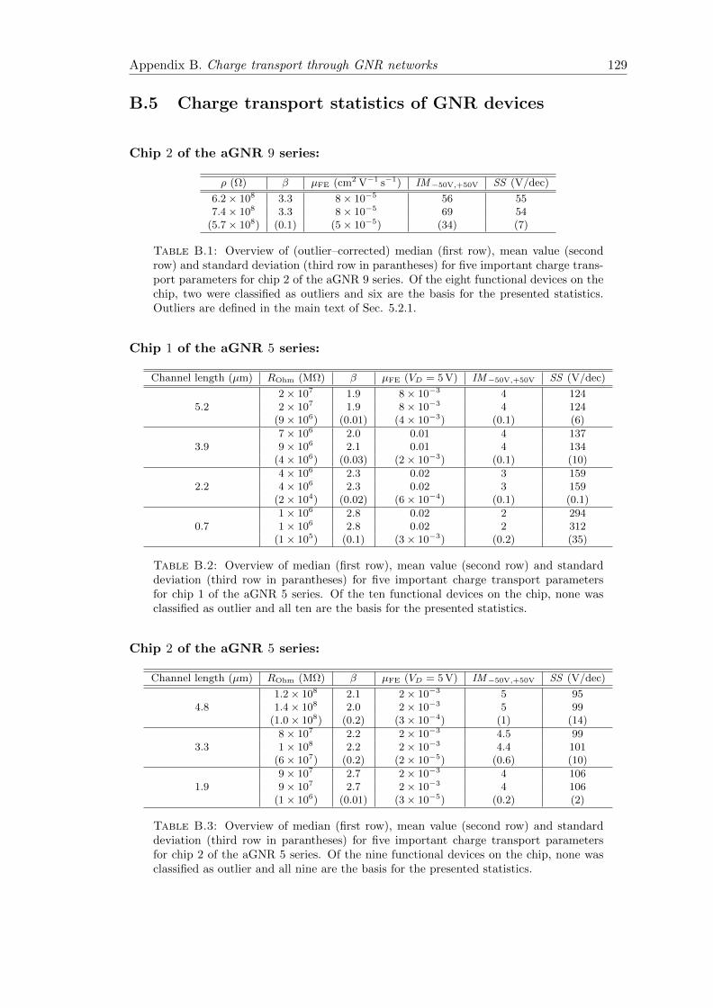
Appendix B. Charge transport through GNR networks 129
B.5 Charge transport statistics of GNR devices
Chip 2 of the aGNR 9 series:
ρ (Ω) β µFE (cm2 V−1 s−1) IM−50V,+50V SS (V/dec)
6.2 × 10⁸ 3.3 8 × 10⁻⁵ 56 557.4 × 10⁸ 3.3 8 × 10⁻⁵ 69 54
(5.7 × 10⁸) (0.1) (5 × 10⁻⁵) (34) (7)
Table B.1: Overview of (outlier–corrected) median (first row), mean value (secondrow) and standard deviation (third row in parantheses) for five important charge trans-port parameters for chip 2 of the aGNR 9 series. Of the eight functional devices on thechip, two were classified as outliers and six are the basis for the presented statistics.Outliers are defined in the main text of Sec. 5.2.1.
Chip 1 of the aGNR 5 series:
Channel length (µm) ROhm (MΩ) β µFE (VD = 5 V) IM−50V,+50V SS (V/dec)
2 × 10⁷ 1.9 8 × 10⁻³ 4 1245.2 2 × 10⁷ 1.9 8 × 10⁻³ 4 124
(9 × 10⁶) (0.01) (4 × 10⁻³) (0.1) (6)
7 × 10⁶ 2.0 0.01 4 1373.9 9 × 10⁶ 2.1 0.01 4 134
(4 × 10⁶) (0.03) (2 × 10⁻³) (0.1) (10)
4 × 10⁶ 2.3 0.02 3 1592.2 4 × 10⁶ 2.3 0.02 3 159
(2 × 10⁴) (0.02) (6 × 10⁻⁴) (0.1) (0.1)
1 × 10⁶ 2.8 0.02 2 2940.7 1 × 10⁶ 2.8 0.02 2 312
(1 × 10⁵) (0.1) (3 × 10⁻³) (0.2) (35)
Table B.2: Overview of median (first row), mean value (second row) and standarddeviation (third row in parantheses) for five important charge transport parametersfor chip 1 of the aGNR 5 series. Of the ten functional devices on the chip, none wasclassified as outlier and all ten are the basis for the presented statistics.
Chip 2 of the aGNR 5 series:
Channel length (µm) ROhm (MΩ) β µFE (VD = 5 V) IM−50V,+50V SS (V/dec)
1.2 × 10⁸ 2.1 2 × 10⁻³ 5 954.8 1.4 × 10⁸ 2.0 2 × 10⁻³ 5 99
(1.0 × 10⁸) (0.2) (3 × 10⁻⁴) (1) (14)
8 × 10⁷ 2.2 2 × 10⁻³ 4.5 993.3 1 × 10⁸ 2.2 2 × 10⁻³ 4.4 101
(6 × 10⁷) (0.2) (2 × 10⁻⁵) (0.6) (10)
9 × 10⁷ 2.7 2 × 10⁻³ 4 1061.9 9 × 10⁷ 2.7 2 × 10⁻³ 4 106
(1 × 10⁶) (0.01) (3 × 10⁻⁵) (0.2) (2)
Table B.3: Overview of median (first row), mean value (second row) and standarddeviation (third row in parantheses) for five important charge transport parametersfor chip 2 of the aGNR 5 series. Of the nine functional devices on the chip, none wasclassified as outlier and all nine are the basis for the presented statistics.
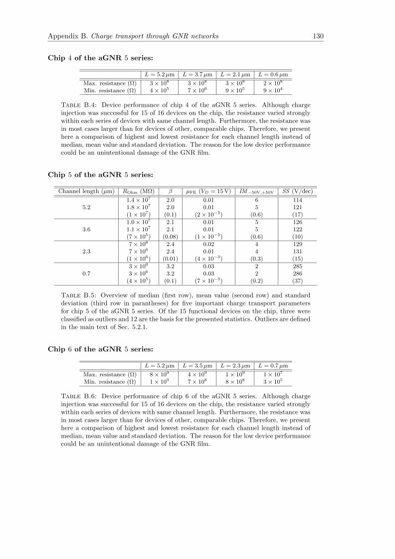
Appendix B. Charge transport through GNR networks 130
Chip 4 of the aGNR 5 series:
L = 5.2µm L = 3.7µm L = 2.1µm L = 0.6µm
Max. resistance (Ω) 3 × 10⁸ 3 × 10⁸ 3 × 10⁸ 2 × 10⁸
Min. resistance (Ω) 4 × 10⁵ 7 × 10⁶ 9 × 10⁵ 9 × 10⁴
Table B.4: Device performance of chip 4 of the aGNR 5 series. Although chargeinjection was successful for 15 of 16 devices on the chip, the resistance varied stronglywithin each series of devices with same channel length. Furthermore, the resistance wasin most cases larger than for devices of other, comparable chips. Therefore, we presenthere a comparison of highest and lowest resistance for each channel length instead ofmedian, mean value and standard deviation. The reason for the low device performancecould be an unintentional damage of the GNR film.
Chip 5 of the aGNR 5 series:
Channel length (µm) ROhm (MΩ) β µFE (VD = 15 V) IM−50V,+50V SS (V/dec)
1.4 × 10⁷ 2.0 0.01 6 1145.2 1.8 × 10⁷ 2.0 0.01 5 121
(1 × 10⁷) (0.1) (2 × 10⁻³) (0.6) (17)
1.0 × 10⁷ 2.1 0.01 5 1263.6 1.1 × 10⁷ 2.1 0.01 5 122
(7 × 10⁵) (0.08) (1 × 10⁻³) (0.6) (10)
7 × 10⁶ 2.4 0.02 4 1292.3 7 × 10⁶ 2.4 0.01 4 131
(1 × 10⁶) (0.01) (4 × 10⁻³) (0.3) (15)
3 × 10⁶ 3.2 0.03 2 2850.7 3 × 10⁶ 3.2 0.03 2 286
(4 × 10⁵) (0.1) (7 × 10⁻³) (0.2) (37)
Table B.5: Overview of median (first row), mean value (second row) and standarddeviation (third row in parantheses) for five important charge transport parametersfor chip 5 of the aGNR 5 series. Of the 15 functional devices on the chip, three wereclassified as outliers and 12 are the basis for the presented statistics. Outliers are definedin the main text of Sec. 5.2.1.
Chip 6 of the aGNR 5 series:
L = 5.2µm L = 3.5µm L = 2.3µm L = 0.7µm
Max. resistance (Ω) 8 × 10⁹ 4 × 10⁹ 1 × 10⁹ 1 × 10⁷
Min. resistance (Ω) 1 × 10⁹ 7 × 10⁸ 8 × 10⁸ 3 × 10⁵
Table B.6: Device performance of chip 6 of the aGNR 5 series. Although chargeinjection was successful for 15 of 16 devices on the chip, the resistance varied stronglywithin each series of devices with same channel length. Furthermore, the resistance wasin most cases larger than for devices of other, comparable chips. Therefore, we presenthere a comparison of highest and lowest resistance for each channel length instead ofmedian, mean value and standard deviation. The reason for the low device performancecould be an unintentional damage of the GNR film.
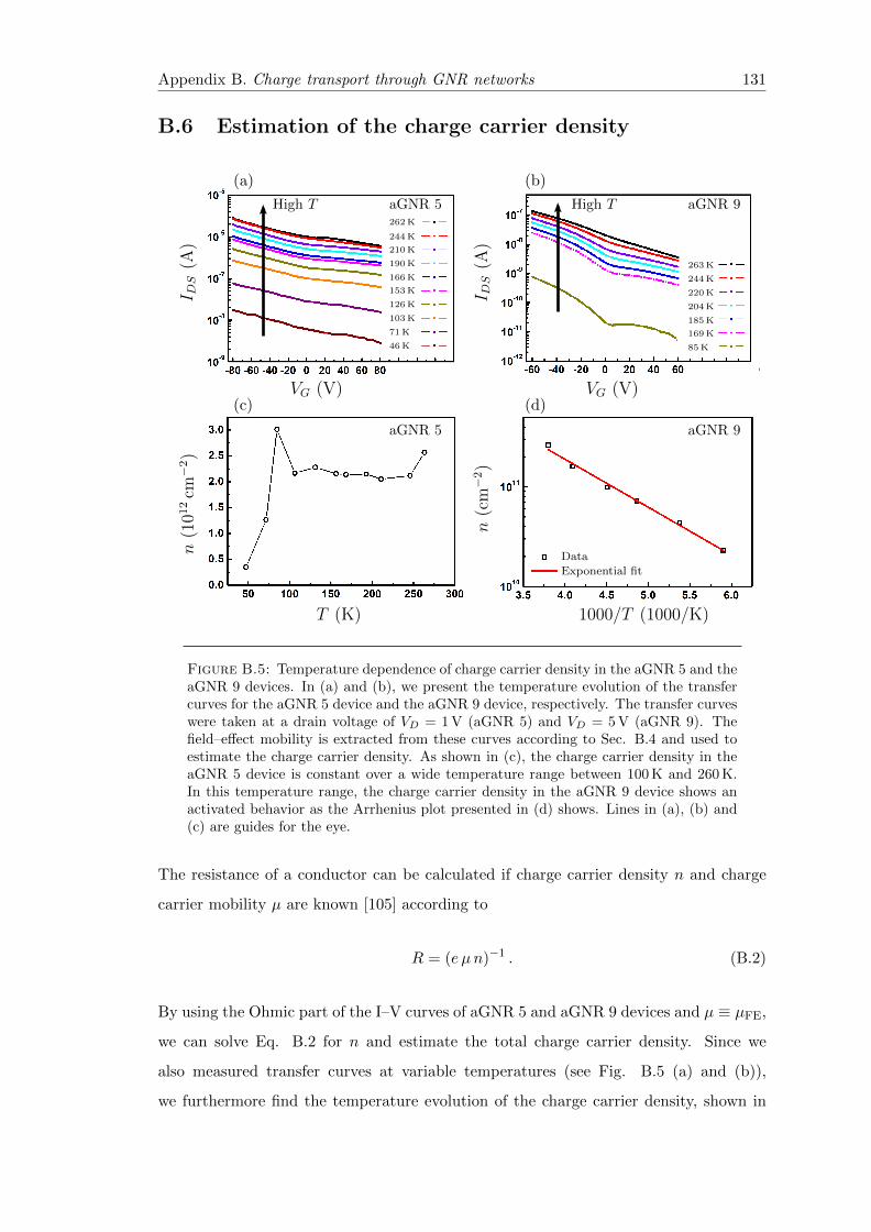
Appendix B. Charge transport through GNR networks 131
B.6 Estimation of the charge carrier density
(a)I D
S(A
)
VG (V)
High T aGNR 5262 K
244 K
210 K
190 K
166 K
153 K
126 K
103 K
71 K
46 K
(b)
I DS
(A)
VG (V)
High T aGNR 9
263 K
244 K
220 K
204 K
185 K
169 K
85 K
(c)
aGNR 5
n(1
012
cm−
2)
T (K)
(d)
n(c
m−
2)
1000/T (1000/K)
aGNR 9
DataExponential fit
Figure B.5: Temperature dependence of charge carrier density in the aGNR 5 and theaGNR 9 devices. In (a) and (b), we present the temperature evolution of the transfercurves for the aGNR 5 device and the aGNR 9 device, respectively. The transfer curveswere taken at a drain voltage of VD = 1 V (aGNR 5) and VD = 5 V (aGNR 9). Thefield–effect mobility is extracted from these curves according to Sec. B.4 and used toestimate the charge carrier density. As shown in (c), the charge carrier density in theaGNR 5 device is constant over a wide temperature range between 100 K and 260 K.In this temperature range, the charge carrier density in the aGNR 9 device shows anactivated behavior as the Arrhenius plot presented in (d) shows. Lines in (a), (b) and(c) are guides for the eye.
The resistance of a conductor can be calculated if charge carrier density n and charge
carrier mobility µ are known [105] according to
R = (e µn)−1 . (B.2)
By using the Ohmic part of the I–V curves of aGNR 5 and aGNR 9 devices and µ ≡ µFE,
we can solve Eq. B.2 for n and estimate the total charge carrier density. Since we
also measured transfer curves at variable temperatures (see Fig. B.5 (a) and (b)),
we furthermore find the temperature evolution of the charge carrier density, shown in
Appendix B. Charge transport through GNR networks 132
Fig. B.5 (c) and (d) for aGNR 5 and aGNR 9, respectivley. Since we are interested
in the temperature evolution of the Ohmic low–bias regime, we determine µFE at a
drain voltage as low as possible. For the aGNR 5 device, we therefore use VD = 1 V
and VD = 5 V for the aGNR 9 device. At 260 K, the charge carrier density is high with
approximately 2×1012 cm−2 and ≈ 3×1011 cm−2 for the aGNR 5 device and the aGNR 9
device, respectively. This justifies the use of Eq. 2.29, which requires equal hopping steps
through the device channel. For the aGNR 5 device, the charge carrier density remains
constant from 260 K down to approximately 100 K. Only at lower temperatures, the
carrier density seems to decrease. Measuring at lower temperatures however is impeded
due to the low current levels. In the case of the aGNR 9 device, we find an activated
behavior of the charge carrier density, allowing us to determine the activation energy
with the help of an Arrhenius plot. We use an exponential model n ∝ exp(− EA
2 kB T
)to determine the activation energy as EA = (191 ± 8) meV. Since we assume, that
the charge carrier density is dominated by extrinsic charge carriers, we attribute this
activation energy to the extrinsic dopants and not to intrinsic carriers from the valence
band of the GNRs.
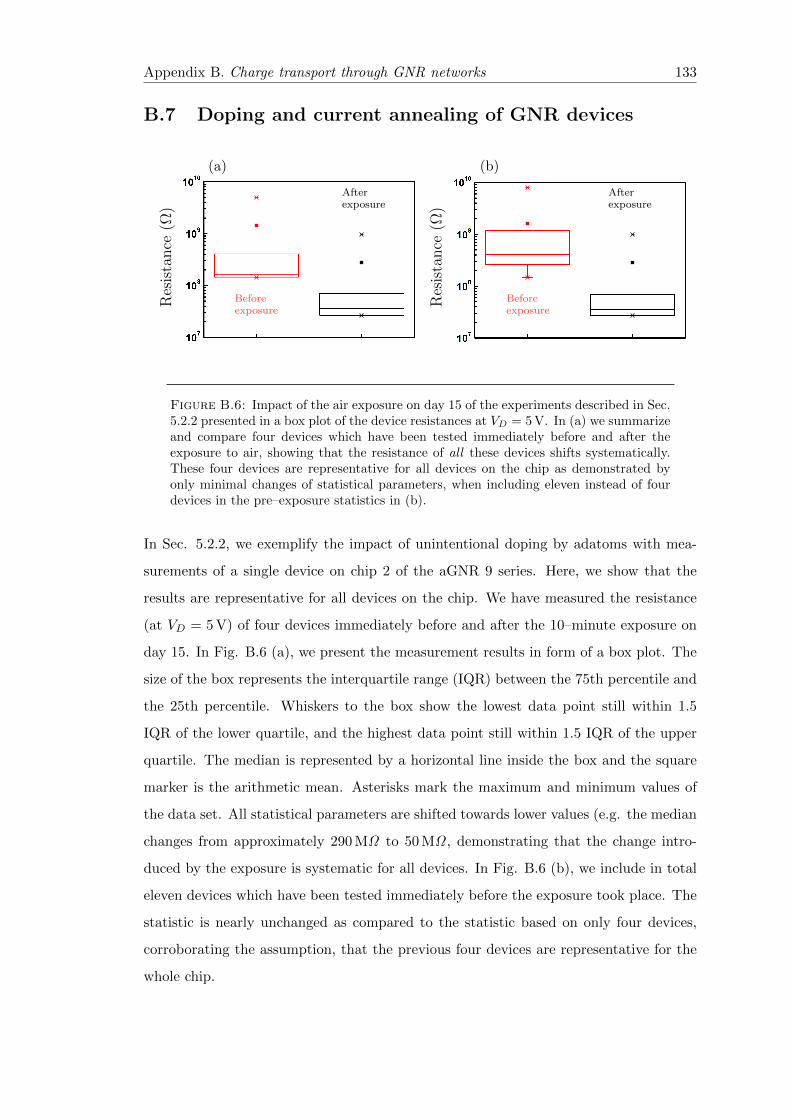
Appendix B. Charge transport through GNR networks 133
B.7 Doping and current annealing of GNR devices
(a)R
esis
tance
(Ω)
Beforeexposure
Afterexposure
(b)
Res
ista
nce
(Ω)
Beforeexposure
Afterexposure
Figure B.6: Impact of the air exposure on day 15 of the experiments described in Sec.5.2.2 presented in a box plot of the device resistances at VD = 5 V. In (a) we summarizeand compare four devices which have been tested immediately before and after theexposure to air, showing that the resistance of all these devices shifts systematically.These four devices are representative for all devices on the chip as demonstrated byonly minimal changes of statistical parameters, when including eleven instead of fourdevices in the pre–exposure statistics in (b).
In Sec. 5.2.2, we exemplify the impact of unintentional doping by adatoms with mea-
surements of a single device on chip 2 of the aGNR 9 series. Here, we show that the
results are representative for all devices on the chip. We have measured the resistance
(at VD = 5 V) of four devices immediately before and after the 10–minute exposure on
day 15. In Fig. B.6 (a), we present the measurement results in form of a box plot. The
size of the box represents the interquartile range (IQR) between the 75th percentile and
the 25th percentile. Whiskers to the box show the lowest data point still within 1.5
IQR of the lower quartile, and the highest data point still within 1.5 IQR of the upper
quartile. The median is represented by a horizontal line inside the box and the square
marker is the arithmetic mean. Asterisks mark the maximum and minimum values of
the data set. All statistical parameters are shifted towards lower values (e.g. the median
changes from approximately 290 MΩ to 50 MΩ , demonstrating that the change intro-
duced by the exposure is systematic for all devices. In Fig. B.6 (b), we include in total
eleven devices which have been tested immediately before the exposure took place. The
statistic is nearly unchanged as compared to the statistic based on only four devices,
corroborating the assumption, that the previous four devices are representative for the
whole chip.
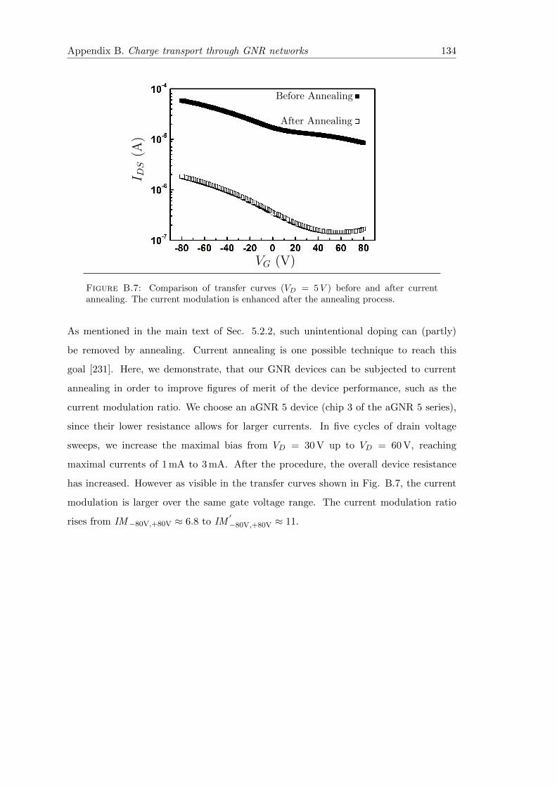
Appendix B. Charge transport through GNR networks 134
VG (V)
I DS
(A)
Before Annealing
After Annealing
Figure B.7: Comparison of transfer curves (VD = 5V ) before and after currentannealing. The current modulation is enhanced after the annealing process.
As mentioned in the main text of Sec. 5.2.2, such unintentional doping can (partly)
be removed by annealing. Current annealing is one possible technique to reach this
goal [231]. Here, we demonstrate, that our GNR devices can be subjected to current
annealing in order to improve figures of merit of the device performance, such as the
current modulation ratio. We choose an aGNR 5 device (chip 3 of the aGNR 5 series),
since their lower resistance allows for larger currents. In five cycles of drain voltage
sweeps, we increase the maximal bias from VD = 30 V up to VD = 60 V, reaching
maximal currents of 1 mA to 3 mA. After the procedure, the overall device resistance
has increased. However as visible in the transfer curves shown in Fig. B.7, the current
modulation is larger over the same gate voltage range. The current modulation ratio
rises from IM−80V,+80V ≈ 6.8 to IM′−80V,+80V ≈ 11.
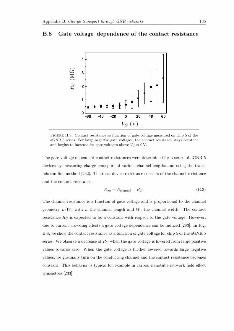
Appendix B. Charge transport through GNR networks 135
B.8 Gate voltage–dependence of the contact resistance
VG (V)
RC
(MΩ
)
Figure B.8: Contact resistance as function of gate voltage measured on chip 5 of theaGNR 5 series. For large negative gate voltages, the contact resistance stays constantand begins to increase for gate voltages above VG ≈ 0 V.
The gate voltage dependent contact resistances were determined for a series of aGNR 5
devices by measuring charge transport at various channel lengths and using the trans-
mission line method [232]. The total device resistance consists of the channel resistance
and the contact resistance,
Ron = Rchannel +RC . (B.3)
The channel resistance is a function of gate voltage and is proportional to the channel
geometry L/W , with L the channel length and W , the channel width. The contact
resistance RC is expected to be a constant with respect to the gate voltage. However,
due to current crowding effects a gate voltage dependence can be induced [283]. In Fig.
B.8, we show the contact resistance as a function of gate voltage for chip 5 of the aGNR 5
series. We observe a decrease of RC when the gate voltage is lowered from large positive
values towards zero. When the gate voltage is further lowered towards large negative
values, we gradually turn on the conducting channel and the contact resistance becomes
constant. This behavior is typical for example in carbon nanotube network field effect
transistors [233].
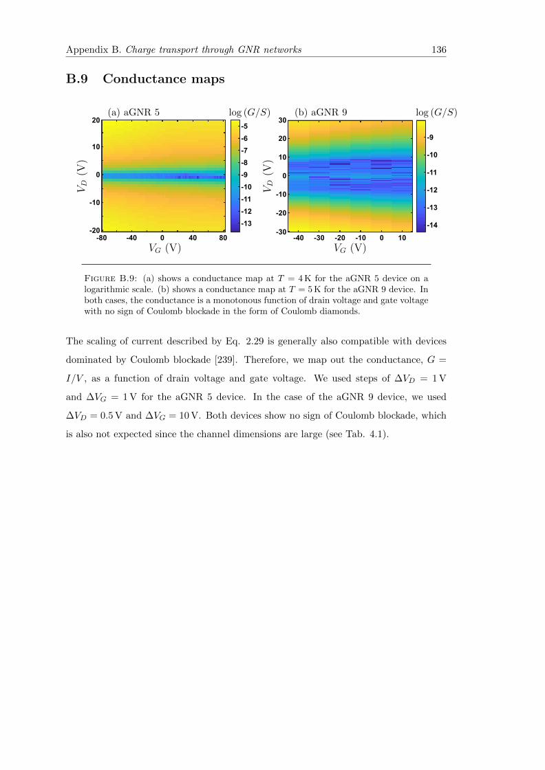
Appendix B. Charge transport through GNR networks 136
B.9 Conductance maps
-5
-6
-7
-8
-9
-10
-11
-12
-13
-80 -40 0 40 80-20
20
-9
-10
-11
-12
-13
-14
0
-10
10
30
-30
0
-10
-20
20
10
-40 -20 0 10-10-30
(a) aGNR 5
VD
(V)
VG (V)
log (G/S) (b) aGNR 9
VD
(V)
VG (V)
log (G/S)
Figure B.9: (a) shows a conductance map at T = 4 K for the aGNR 5 device on alogarithmic scale. (b) shows a conductance map at T = 5 K for the aGNR 9 device. Inboth cases, the conductance is a monotonous function of drain voltage and gate voltagewith no sign of Coulomb blockade in the form of Coulomb diamonds.
The scaling of current described by Eq. 2.29 is generally also compatible with devices
dominated by Coulomb blockade [239]. Therefore, we map out the conductance, G =
I/V , as a function of drain voltage and gate voltage. We used steps of ∆VD = 1 V
and ∆VG = 1 V for the aGNR 5 device. In the case of the aGNR 9 device, we used
∆VD = 0.5 V and ∆VG = 10 V. Both devices show no sign of Coulomb blockade, which
is also not expected since the channel dimensions are large (see Tab. 4.1).
Appendix B. Charge transport through GNR networks 137
B.10 Temperature dependence of magnetotransport
Temperature (K) a (T−2)
4 (2060 ± 4) × 10−6
10 (1131 ± 5) × 10−6
19 (423 ± 2) × 10−6
28 (247 ± 2) × 10−6
37 (160 ± 2) × 10−6
Table B.7: Overview of the temperature dependence of the fitting parameter a in afitting model ∆ρ/ρ = aB2, where ∆ρ/ρ is the relative change in resistivity and B isthe magnetic field (see Sec. 5.3.2 for details).

Appendix C
Additional material for Chapter 7
139
Appendix C. Properties of chromium trihalides 140
C.1 Additional experimental details
Number Species Measurement Configuration Mass (µg) Mass error (µg)
1 CrI3 H ‖ c 0.60 0.032 CrI3 H ‖ c 0.6 0.13 CrI3 H ⊥ c 1.05 0.044 CrBr3 H ‖ c 3.2 0.15 CrBr3 H ‖ c 1.4 0.16 CrBr3 H ⊥ c 0.77 0.067 CrCl3 H ‖ c 1.45 0.048 CrCl3 H ⊥ c 0.66 0.10
Table C.1: Experimentally determined masses of CrX3 crystals.
The mass densities of the CrX3 compounds are ρCrI3 = 5.33 g/cm3 [284], ρCrBr3 =
4.60 g/cm3 [284] and ρCrI3 = 2.95 g/cm3 [273].
Appendix C. Properties of chromium trihalides 141
C.2 Hysteresis loops of chromium trihalides
CrI3, H ⊥ c CrI3, H ‖ c
CrBr3, H ⊥ c CrBr3, H ‖ c
CrCl3, H ⊥ c CrCl3, H ‖ c
Mag
net
icM
omen
t(emu
)
Mag
net
icM
omen
t(emu
)
Magnetic Field µ0H (T ) Magnetic Field µ0H (T )
Mag
net
icM
omen
t(emu
)
Mag
net
icM
omen
t(emu
)
Magnetic Field µ0H (T ) Magnetic Field µ0H (T )
Mag
net
icM
omen
t(emu
)
Mag
net
icM
omen
t(emu
)
Magnetic Field µ0H (T ) Magnetic Field µ0H (T )
Figure C.1: Full hysteresis loops for all CrX3 compounds at a temperature of 10 K inboth measurement configurations. The error of the magnetic measurements are smallas discussed in the main text in 7.4 and are not shown here in order to enhance thefocus on the shape and features of the measurement curves. Lines are a guide for theeye.
Appendix C. Properties of chromium trihalides 142
C.3 Degradation of chromium bromide in air
(a) (b)
500µm 500µm
Figure C.2: Degradation of an exfoliated CrBr3 crystal. In (a), the image was taken5 min after exfoliation and in (b), the image was taken 30 min after exfoliation. Macro-scopic changes are visible with a clear loss of the original crystal structure. I thank D.W. with whom the exfoliation experiments have been performed together.
Bibliography
[1] K. S. Novoselov, A. K. Geim, S. V. Morozov, D. Jiang, Y. Zhang, S. V. Dubonos,
I. V. Grigorieva, and A. A. Firsov. Electric Field Effect in Atomically Thin Carbon
Films. Science, 306(5696):666, 2004. doi: 10.1126/science.1102896.
[2] K. S. Novoselov, D. Jiang, F. Schedin, T. J. Booth, V. V. Khotkevich, S. V.
Morozov, and A. K. Geim. Two-Dimensional Atomic Crystals. Proceedings of the
National Academy of Sciences of the United States of America, 102(30):10451–
10453, 2005. doi: 10.1073/pnas.0502848102.
[3] X. Li and H. Zhu. Two-dimensional MoS2: Properties, Preparation, and Applica-
tions. Journal of Materiomics, 1(1):33, 2015. doi: 10.1016/j.jmat.2015.03.003.
[4] L. Li, Y. Yu, G. J. Ye, Q. Ge, X. Ou, H. Wu, D. Feng, Xian H. Chen, and
Y. Zhang. Black Phosphorus Field-Effect Transistors. Nature Nanotechnology, 9
(5):372, 2014. doi: 10.1038/nnano.2014.35.
[5] K. Nakada, M. Fujita, G. Dresselhaus, and M. S. Dresselhaus. Edge State in
Graphene Ribbons: Nanometer Size Effect and Edge Shape Dependence. Physical
Review B, 54(24):17954, 1996. doi: 10.1103/PhysRevB.54.17954.
[6] L. Yang, C.-H. Park, Y.-W. Son, M. Cohen, and S. Louie. Quasiparticle Energies
and Band Gaps in Graphene Nanoribbons. Physical Review Letters, 99(18):186801,
2007. doi: 10.1103/PhysRevLett.99.186801.
[7] O. V. Yazyev and M. I. Katsnelson. Magnetic Correlations at Graphene Edges:
Basis for Novel Spintronics Devices. Physical Review Letters, 100(4):047209, 2008.
doi: 10.1103/PhysRevLett.100.047209.
[8] F. Joucken, Y. Tison, P. Le Fevre, A. Tejeda, A. Taleb-Ibrahimi, E. Conrad,
V. Repain, C. Chacon, A. Bellec, Y. Girard, S. Rousset, J. Ghijsen, R. Sporken,
143
Bibliography 144
H. Amara, F. Ducastelle, and J. Lagoute. Charge Transfer and Electronic Doping
in Nitrogen–Doped Graphene. Scientific Reports, 5:14564, 2015. doi: 10.1038/
srep14564.
[9] L. D’Arsie, S. Esconjauregui, R. Weatherup, Y. Guo, S. Bhardwaj, A. Centeno,
A. Zurutuza, C. Cepek, and J. Robertson. Stability of Graphene Doping with
MoO3 and I2. Applied Physics Letters, 105(10):103103, 2014. doi: 10.1063/1.
4895025.
[10] J. Meyer, P. R. Kidambi, B. C. Bayer, C. Weijtens, A. Kuhn, A. Centeno, A. Pes-
quera, A. Zurutuza, J. Robertson, and S. Hofmann. Metal Oxide Induced Charge
Transfer Doping and Band Alignment of Graphene Electrodes for Efficient Organic
Light Emitting Diodes. Scientific Reports, 4(5380), 2014. doi: 10.1038/srep05380.
[11] H. I. Wang, M.-L. Braatz, N. Richter, K.-J. Tielrooij, Z. Mics, H. Lu, N.-E. Weber,
K. Mullen, D. Turchinovich, M. Klaui, and M. Bonn. Reversible Photochemical
Control of Doping Levels in Supported Graphene. The Journal of Physical Chem-
istry C, 121(7):4083, 2017. doi: 10.1021/acs.jpcc.7b00347.
[12] H. Gao, L. Wang, J. Zhao, F. Ding, and J. Lu. Band Gap Tuning of Hydrogenated
Graphene: H Coverage and Configuration Dependence. The Journal of Physical
Chemistry C, 115(8):3236, 2011. doi: 10.1021/jp1094454.
[13] D. C. Elias, R. R. Nair, T. M. G. Mohiuddin, S. V. Morozov, P. Blake, M. P.
Halsall, A. C. Ferrari, D. W. Boukhvalov, M. I. Katsnelson, A. K. Geim, and
K. S. Novoselov. Control of Graphene’s Properties by Reversible Hydrogenation:
Evidence for Graphane. Science, 323:610, 2009. doi: 10.1126/science.1167130.
[14] B. R. Matis, J. S. Burgess, F. A. Bulat, A. L. Friedman, B. H. Houston, and J. W.
Baldwin. Surface Doping and Band Gap Tunability in Hydrogenated Graphene.
ACS Nano, 6(1):17, 2012. doi: 10.1021/nn2034555.
[15] S. Agnoli and M. Favaro. Doping Graphene with Boron: A Review of Synthesis
Methods, Physicochemical Characterization, and Emerging Applications. Journal
of Materials Chemistry A, 4(14):5002, 2016. doi: 10.1039/C5TA10599D.
[16] Y.-B. Tang, L.-C. Yin, Y. Yang, X.-H. Bo, Y.-L. Cao, H.-E. Wang, W.-J. Zhang,
I. Bello, S.-T. Lee, H.-M. Cheng, and C.-S. Lee. Tunable Band Gaps and p-
Type Transport Properties of Boron-Doped Graphenes by Controllable Ion Doping
Bibliography 145
Using Reactive Microwave Plasma. ACS Nano, 6(3):1970, 2012. doi: 10.1021/
nn3005262.
[17] S. H. Park, J. Chae, M.-H. Cho, J. H. Kim, K.-H. Yoo, S. W. Cho, T. G. Kim,
and J. W. Kim. High Concentration of Nitrogen Doped into Graphene using N2
Plasma with an Aluminum Oxide Buffer Layer. J. Mater. Chem. C, 2(5):933,
2014. doi: 10.1039/C3TC31773K.
[18] Y. Xue, B. Wu, L. Jiang, Y. Guo, L. Huang, J. Chen, J. Tan, D. Geng, B. Luo,
W. Hu, G. Yu, and Y. Liu. Low Temperature Growth of Highly Nitrogen-Doped
Single Crystal Graphene Arrays by Chemical Vapor Deposition. Journal of the
American Chemical Society, 134(27):11060, 2012. doi: 10.1021/ja302483t.
[19] J.-G. Park. Opportunities and Challenges of 2d Magnetic van der Waals Materials:
Magnetic Graphene? Journal of Physics: Condensed Matter, 28(30):301001, 2016.
doi: 10.1088/0953-8984/28/30/301001.
[20] B. Huang, G. Clark, E. Navarro-Moratalla, D. R. Klein, R. Cheng, K. L. Seyler,
D. Zhong, E. Schmidgall, M. A. McGuire, D. H. Cobden, W. Yao, D. Xiao,
P. Jarillo-Herrero, and X. Xu. Layer–Dependent Ferromagnetism in a van der
Waals Crystal down to the Monolayer Limit. Nature, 546(7657):270, 2017. doi:
10.1038/nature22391.
[21] N. Richter, D. Weber, F. Martin, N. Singh, U. Schwingenschlogl, B. V. Lotsch, and
M. Klaui. Temperature–dependent magnetic anisotropy in the layered magnetic
semiconductors Cri3 and CrBr3. Physical Review Materials, 2(2):024004, 2018.
doi: 10.1103/PhysRevMaterials.2.024004.
[22] M. A. McGuire, H. Dixit, V. R. Cooper, and B. C. Sales. Coupling of Crystal
Structure and Magnetism in the Layered, Ferromagnetic Insulator CrI3. Chemistry
of Materials, 27(2):612, 2015. doi: 10.1021/cm504242t.
[23] I. Tsubokawa. On the Magnetic Properties of a CrBr3 Single Crystal. Journal of
the Physical Society of Japan, 15:1664, 1960. doi: 10.1143/JPSJ.15.1664.
[24] J. F. Dillon. Ferromagnetic Resonance in CrBr3. Journal of Applied Physics, 33
(3):1191, 1962. doi: 10.1063/1.1728652.
Bibliography 146
[25] J. F. Dillon and C. E. Olson. Magnetization, Resonance, and Optical Properties
of the Ferromagnet CrI3. Journal of Applied Physics, 36(3):1259, 1965. doi: 10.
1063/1.1714194.
[26] W. N. Hansen. Some Magnetic Properties of the Chromium ( III ) Halides at
4.2K. Journal of Applied Physics, 30(4):304, 1959. doi: 10.1063/1.2185944.
[27] K. S. Novoselov, A. Mishchenko, A. Carvalho, and A. H. Castro Neto. 2D Materials
and van der Waals Heterostructures. Science, 353(6298):9439, 2016. doi: 10.1126/
science.aac9439.
[28] D. Zhong, K. L. Seyler, X. Linpeng, R. Cheng, N. Sivadas, B. Huang,
E. Schmidgall, T. Taniguchi, K. Watanabe, M. A. McGuire, W. Yao, D. Xiao,
K.-M. C. Fu, and X. Xu. Van der Waals Engineering of Ferromagnetic Semi-
conductor Heterostructures for Spin and Valleytronics. Science Advances, 3(5):
e1603113, 2017. doi: 10.1126/sciadv.1603113.
[29] A. H. Castro Neto, F. Guinea, N. M. R. Peres, K. S. Novoselov, and A. K. Geim.
The Electronic Properties of Graphene. Reviews of Modern Physics, 81(1):109,
2009. doi: 10.1103/RevModPhys.81.109.
[30] L. Onsager. Crystal Statistics. I. A Two-Dimensional Model with an Order–
Disorder Transition. Physical Review, 65(3):117, 1944. doi: 10.1103/PhysRev.
65.117.
[31] J. H. Davies. The Physics of Low-dimensional Semiconductors: An Introduction.
Cambridge University Press, Cambridge, 1997. ISBN 978-0-521-48148-9. doi:
10.1017/CBO9780511819070.
[32] W. W. Chow and S. W. Koch. Basic Concepts. In W. W. Chow and S. W. Koch,
editors, Semiconductor-Laser Fundamentals: Physics of the Gain Materials, pages
1–35. Springer Berlin Heidelberg, Berlin, Heidelberg, 1999. ISBN 978-3-662-03880-
2. doi: 10.1007/978-3-662-03880-2\ 1.
[33] K. K. Ng. A Survey of Semiconductor Devices. IEEE Transactions on Electron
Devices, 43(10):1760, 1996. doi: 10.1109/16.536822.
[34] L. Van Hove. The Occurrence of Singularities in the Elastic Frequency Distribution
of a Crystal. Physical Review, 89(6):1189, 1953.
Bibliography 147
[35] A. Hirsch. The Era of Carbon Allotropes. Nature materials, 9(11):868, 2010. doi:
10.1038/nmat2885.
[36] P. R. Wallace. The Band Theory of Graphite. Physical Review, 71(9):622, 1947.
doi: 10.1103/PhysRev.71.622.
[37] J. C. Slater and G. F. Koster. Simplified LCAO Method for the Periodic Potential
Problem. Physical Review, 94(6):1498, 1954. doi: 10.1103/PhysRev.94.1498.
[38] C. Bena and G. Montambaux. Remarks on the Tight–Binding Model of Graphene.
New Journal of Physics, 11(9):095003, 2009. doi: 10.1088/1367-2630/11/9/
095003.
[39] E. Wigner and F. Seitz. On the Constitution of Metallic Sodium. Physical Review,
43(10):804, 1933. doi: 10.1103/PhysRev.43.804.
[40] M. O. Goerbig, J.-N. Fuchs, G. Montambaux, and F. Piechon. Tilted Anisotropic
Dirac Cones in Quinoid–Type Graphene and alpha-(BEDT-TTF)2I3. Physical
Review B, 78(4):045415, 2008. doi: 10.1103/PhysRevB.78.045415.
[41] S. Reich, J. Maultzsch, C. Thomsen, and P. Ordejon. Tight–Binding Description
of Graphene. Physical Review B, 66(3):035412, 2002. doi: 10.1103/PhysRevB.66.
035412.
[42] R. S. Deacon, K.-C. Chuang, R. J. Nicholas, K. S. Novoselov, and A. K. Geim. Cy-
clotron Resonance Study of the Electron and Hole Velocity in Graphene Monolay-
ers. Physical Review B, 76(8):081406(R), 2007. doi: 10.1103/PhysRevB.76.081406.
[43] G. W. Semenoff. Condensed–Matter Simulation of a Three–Dimensional Anomaly.
Physical Review Letters, 53(26):2449, 1984. doi: 10.1103/PhysRevLett.53.2449.
[44] M. M. Grujic. Manifestations of Intrinsic and Induced Magnetic Properties of
Graphene Nanostructures. PhD Thesis. University of Antwerp, 2015.
[45] J. C. Slonczewski and P. R. Weiss. Band Structure of Graphite. Physical Review,
109(2):272, 1958. doi: 10.1103/PhysRev.109.272.
[46] J. W. McClure. Theory of Diamagnetism of Graphite. Phys. Rev., 119(2):606,
1960. doi: 10.1103/PhysRev.119.606.
Bibliography 148
[47] S. Shallcross, S. Sharma, E. Kandelaki, and O. A. Pankratov. Electronic Structure
of Turbostratic Graphene. Physical Review B, 81(16):165105, 2010. doi: 10.1103/
PhysRevB.81.165105.
[48] X. Zhang, O. V. Yazyev, J. Feng, L. Xie, C. Tao, Y.-C. Chen, L. Jiao, Z. Pe-
dramrazi, A. Zettl, S. G. Louie, H. Dai, and M. F. Crommie. Experimentally
Engineering the Edge Termination of Graphene Nanoribbons. ACS Nano, 7(1):
198, 2013. doi: 10.1021/nn303730v.
[49] M. Fujita, K. Wakabayashi, K. Nakada, and K. Kusakabe. Peculiar Localized
State at Zigzag Graphite Edge. Journal of the Physical Society of Japan, 65(7):
1920, 1996. doi: 10.1143/JPSJ.65.1920.
[50] K. Wakabayashi, M. Fujita, H. Ajiki, and M. Sigrist. Electronic and magnetic
properties of nanographite ribbons. Physical Review B, 59(12):8271, 1999. doi:
10.1103/PhysRevB.59.8271.
[51] L. Brey and H. A. Fertig. Electronic States of Graphene Nanoribbons Studied
with the Dirac Equation. Physical Review B, 73(23):235411, 2006. doi: 10.1103/
PhysRevB.73.235411.
[52] A. R. Akhmerov and C. W. J. Beenakker. Boundary Conditions for Dirac Fermions
on a Terminated Honeycomb Lattice. Physical Review B, 77(8):085423, 2008. doi:
10.1103/PhysRevB.77.085423.
[53] K. Wakabayashi, Y. Takane, M. Yamamoto, and M. Sigrist. Electronic Transport
Properties of Graphene Nanoribbons. New Journal of Physics, 11(9):095016, 2009.
doi: 10.1088/1367-2630/11/9/095016.
[54] Y.-W. Son, M. L. Cohen, and S. G. Louie. Energy Gaps in Graphene Nanorib-
bons. Physical Review Letters, 97(21):216803, 2006. doi: 10.1103/PhysRevLett.
97.216803.
[55] V. Barone, O. Hod, and G. E. Scuseria. Electronic Structure and Stability of
Semiconducting Graphene Nanoribbons. Nano Letters, 6(12):2748, 2006. doi:
10.1021/nl0617033.
Bibliography 149
[56] Y. Miyamoto, K. Nakada, and M. Fujita. First–Principles Study of Edge States
of H–Terminated Graphitic Ribbons. Physical Review B, 59(15):9858, 1999. doi:
10.1103/PhysRevB.59.9858.
[57] J. A. Verges, G. Chiappe, and E. Louis. On the Forbidden Gap of Finite Graphene
Nanoribbons. The European Physical Journal B, 88(8):200, 2015. doi: 10.1140/
epjb/e2015-60389-5.
[58] L. Pisani, J. A. Chan, B. Montanari, and N. M. Harrison. Electronic Structure
and Magnetic Properties of Graphitic Ribbons. Physical Review B, 75(6):064418,
2007. doi: 10.1103/PhysRevB.75.064418.
[59] J. Jung, T. Pereg-Barnea, and A. H. MacDonald. Theory of Interedge Superex-
change in Zigzag Edge Magnetism. Physical Review Letters, 102(22):227205, 2009.
doi: 10.1103/PhysRevLett.102.227205.
[60] H. Karimi and I. Affleck. Towards a Rigorous Proof of Magnetism on the Edges
of Graphene Nanoribbons. Physical Review B, 86(11):115446, 2012. doi: 10.1103/
PhysRevB.86.115446.
[61] O. V. Yazyev. Emergence of Magnetism in Graphene Materials and Nanostruc-
tures. Reports on Progress in Physics, 73(5):056501, 2010.
[62] F. Munoz Rojas, J. Fernandez-Rossier, and J. J. Palacios. Giant Magnetoresistance
in Ultrasmall Graphene Based Devices. Physical Review Letters, 102(13):136810,
2009. doi: 10.1103/PhysRevLett.102.136810.
[63] Y.-W. Son, M. L. Cohen, and S. G. Louie. Half–Metallic Graphene Nanoribbons.
Nature, 444(7117):347, 2006. doi: 10.1038/nature05180.
[64] N. D. Mermin and H. Wagner. Absence of Ferromagnetism or Antiferromagnetism
in One– or Two–Dimensional Isotropic Heisenberg Models. Physical Review Let-
ters, 17(22):1133, 1966. doi: 10.1103/PhysRevLett.17.1133.
[65] J. Jung and A. H. MacDonald. Carrier Density and Magnetism in Graphene Zigzag
Nanoribbons. Physical Review B, 79(23):235433, 2009. doi: 10.1103/PhysRevB.
79.235433.
Bibliography 150
[66] H. Raza and E. C. Kan. Armchair Graphene Nanoribbons: Electronic Structure
and Electric–Field Modulation. Physical Review B, 77(24):245434, 2008. doi:
10.1103/PhysRevB.77.245434.
[67] H. Zheng, Z. F. Wang, T. Luo, Q. W. Shi, and J. Chen. Analytical Study of
Electronic Structure in Armchair Graphene Nanoribbons. Physical Review B, 75
(16):165414, 2007. doi: 10.1103/PhysRevB.75.165414.
[68] A. V. Rozhkov, S. Savel’ev, and F. Nori. Electronic properties of armchair graphene
nanoribbons. Physical Review B, 79(12):125420, 2009. doi: 10.1103/PhysRevB.
79.125420.
[69] K. Wakabayashi, K.-I. Sasaki, T. Nakanishi, and T. Enoki. Electronic States
of Graphene Nanoribbons and Analytical Solutions. Science and Technology of
Advanced Materials, 11(5):054504, 2010. doi: 10.1088/1468-6996/11/5/054504.
[70] J. Munarriz Arrieta. Tight-Binding Description of Graphene Nanostructures. In
J. Munarriz Arrieta, editor, Modelling of Plasmonic and Graphene Nanodevices,
page 13. Springer International Publishing, 2014. ISBN 978-3-319-07088-9. doi:
10.1007/978-3-319-07088-9 2.
[71] A. D. Zdetsis and E.N. Economou. Rationalizing and Reconciling Energy Gaps and
Quantum Confinement in Narrow Atomically Precise Armchair Graphene Nanorib-
bons. Carbon, 116:422, 2017. doi: 10.1016/j.carbon.2017.02.006.
[72] D. Gunlycke and C. T. White. Tight–Binding Energy Dispersions of Armchair–
Edge Graphene Nanostrips. Physical Review B, 77(11):115116, 2008. doi: 10.
1103/PhysRevB.77.115116.
[73] W. Jaskolski, A. Ayuela, M. Pelc, H. Santos, and L. Chico. Edge States and Flat
Bands in Graphene Nanoribbons with Arbitrary Geometries. Physical Review B,
83(23):235424, 2011. doi: 10.1103/PhysRevB.83.235424.
[74] J. Liu, B.-W. Li, Y.-Z. Tan, A. Giannakopoulos, C. Sanchez-Sanchez, D. Beljonne,
P. Ruffieux, R. Fasel, X. Feng, and K. Mullen. Toward Cove-Edged Low Band
Gap Graphene Nanoribbons. Journal of the American Chemical Society, 137(18):
6097, 2015. doi: 10.1021/jacs.5b03017.
Bibliography 151
[75] C. Tao, L. Jiao, O. V. Yazyev, Y.-C. Chen, J. Feng, X. Zhang, R. B. Capaz, J. M.
Tour, A. Zettl, S. G. Louie, H. Dai, and M. F. Crommie. Spatially Resolving
Edge States of Chiral Graphene Nanoribbons. Nature Physics, 7(8):616, 2011.
doi: 10.1038/nphys1991.
[76] O. V. Yazyev, R. B. Capaz, and S. G. Louie. Theory of Magnetic Edge States
in Chiral Graphene Nanoribbons. Physical Review B, 84(11):115406, 2011. doi:
10.1103/PhysRevB.84.115406.
[77] A. R. Carvalho, J. H. Warnes, and C. H. Lewenkopf. Edge Magnetization and
Local Density of States in Chiral Graphene Nanoribbons. Physical Review B, 89
(24):245444, 2014. doi: 10.1103/PhysRevB.89.245444.
[78] D. G. de Oteyza, A. Garcıa-Lekue, M. Vilas-Varela, N. Merino-Dıez, E. Carbonell-
Sanroma, M. Corso, G. Vasseur, C. Rogero, E. Guitian, J. I. Pascual, J. E.
Ortega, Y. Wakayama, and D. Pena. Substrate–Independent Growth of Atom-
ically Precise Chiral Graphene Nanoribbons. ACS Nano, 10(9):9000, 2016. doi:
10.1021/acsnano.6b05269.
[79] J. Cai, P. Ruffieux, R. Jaafar, M. Bieri, T. Braun, S. Blankenburg, M. Muoth,
A. P. Seitsonen, M. Saleh, X. Feng, K. Mullen, and R. Fasel. Atomically Precise
Bottom–Up Fabrication of Graphene Nanoribbons. Nature, 466(7305):470, 2010.
doi: 10.1038/nature09211.
[80] T. H. Vo, M. Shekhirev, D. A. Kunkel, M. D. Morton, E. Berglund, L. Kong,
P. M. Wilson, P. A. Dowben, A. Enders, and A. Sinitskii. Large–Scale Solution
Synthesis of Narrow Graphene Nanoribbons. Nature Communications, 5(3189),
2014. doi: 10.1038/ncomms4189.
[81] E. C. Girao, L. Liang, E. Cruz-Silva, A. G. S. Filho, and V. Meunier. Emergence of
Atypical Properties in Assembled Graphene Nanoribbons. Physical Review Letters,
107(13):135501, 2011. doi: 10.1103/PhysRevLett.107.135501.
[82] Z. Chen, W. Zhang, C-A. Palma, A. Lodi Rizzini, B. Liu, A. Abbas, N. Richter,
L. Martini, X.-Y. Wang, N. Cavani, H. Lu, N. Mishra, C. Coletti, R. Berger,
F. Klappenberger, M. Klaui, A. Candini, M. Affronte, C. Zhou, V. De Renzi, U. del
Pennino, J. V. Barth, H. J. Rader, A. Narita, X. Feng, and K. Mullen. Synthesis
of Graphene Nanoribbons by Ambient-Pressure Chemical Vapor Deposition and
Bibliography 152
Device Integration. Journal of the American Chemical Society, 138(47):15488,
2016. doi: 10.1021/jacs.6b10374.
[83] V. A. Saroka, K. G. Batrakov, V. A. Demin, and L. A. Chernozatonskii. Band Gaps
in Jagged and Straight Graphene Nanoribbons Tunable by an External Electric
Field. Journal of Physics: Condensed Matter, 27(14):145305, 2015. doi: 10.1088/
0953-8984/27/14/145305.
[84] X. Wu and X. C. Zeng. Sawtooth–Like Graphene Nanoribbon. Nano Research, 1
(1):40, 2008. doi: 10.1007/s12274-008-8001-z.
[85] L. Kou, C. Tang, C. Chen, and W. Guo. Hybrid W–Shaped Graphene Nanorib-
bons: Distinct Electronic and Transport Properties. Journal of Applied Physics,
110(12):124312, 2011. doi: 10.1063/1.3669496.
[86] E. C. Girao, E. Cruz-Silva, L. Liang, A. G. S. Filho, and V. Meunier. Structural
and Electronic Properties of Graphitic Nanowiggles. Physical Review B, 85(23):
235431, 2012. doi: 10.1103/PhysRevB.85.235431.
[87] W. Huang, J.-S. Wang, and G. Liang. Theoretical Study on Thermoelectric Prop-
erties of Kinked Graphene Nanoribbons. Physical Review B, 84(4):045410, 2011.
doi: 10.1103/PhysRevB.84.045410.
[88] Y. Chen, T. Jayasekera, A. Calzolari, K. W. Kim, and M. Buongiorno Nardelli.
Thermoelectric Properties of Graphene Nanoribbons, Junctions and Superlat-
tices. Journal of Physics: Condensed Matter, 22(37):372202, 2010. doi: 10.1088/
0953-8984/22/37/372202.
[89] H. Sevincli, M. Topsakal, and S. Ciraci. Superlattice Structures of Graphene–
Based Armchair Nanoribbons. Physical Review B, 78(24):245402, 2008. doi: 10.
1103/PhysRevB.78.245402.
[90] A. Cresti and S. Roche. Edge–Disorder–Dependent Transport Length Scales in
Graphene Nanoribbons: From Klein Defects to the Superlattice Limit. Physical
Review B, 79(23):233404, 2009. doi: 10.1103/PhysRevB.79.233404.
[91] L. Esaki and R. Tsu. Superlattice and Negative Differential Conductivity in Semi-
conductors. IBM Journal of Research and Development, 14(1):61, 1970. doi:
10.1147/rd.141.0061.
Bibliography 153
[92] S. Ciraci and Inder P. Batra. Long-Range Order and Segregation in Semicon-
ductor Superlattices. Physical Review Letters, 58(20):2114, 1987. doi: 10.1103/
PhysRevLett.58.2114.
[93] L. Liang and V. Meunier. Electronic and Thermoelectric Properties of Assembled
Graphene Nanoribbons with Elastic Strain and Structural Dislocation. Applied
Physics Letters, 102(14):143101, 2013. doi: 10.1063/1.4800777.
[94] L. Liang and V. Meunier. Electronic Structure of Assembled Graphene Nanorib-
bons: Substrate and Many–Body Effects. Physical Review B, 86(19):195404, 2012.
doi: 10.1103/PhysRevB.86.195404.
[95] M. Shishkin and G. Kresse. Self–Consistent GW Calculations for Semiconductors
and Insulators. Physical Review B, 75(23):235102, 2007. doi: 10.1103/PhysRevB.
75.235102.
[96] S. Wang and J. Wang. Quasiparticle Energies and Optical Excitations in Chevron-
Type Graphene Nanoribbon. The Journal of Physical Chemistry C, 116(18):10193,
2012. doi: 10.1021/jp2125872.
[97] Heinz Bassler. Charge Transport in Disordered Organic Photoconductors a Monte
Carlo Simulation Study. physica status solidi (b), 175(1):15, 1993.
[98] Allen Miller and Elihu Abrahams. Impurity Conduction at Low Concentrations.
Physical Review, 120(3):745, 1960.
[99] R. A. Marcus and N. Sutin. Electron Transfers in Chemistry and Biology. Biochim-
ica et Biophysica Acta (BBA)-Reviews on Bioenergetics, 811(3):265, 1985.
[100] K. Asadi, A. J. Kronemeijer, T. Cramer, L. J. A. Koster, P. W. M. Blom, and D. M.
de Leeuw. Polaron Hopping Mediated by Nuclear Tunnelling in Semiconducting
Polymers at High Carrier Density. Nature Communications, 4:1710, 2013. doi:
10.1038/ncomms2708.
[101] N. J. van der Kaap, I. Katsouras, K. Asadi, P. W. M. Blom, L. J. A. Koster,
and D. M. de Leeuw. Charge Transport in Disordered Semiconducting Polymers
Driven by Nuclear Tunneling. Physical Review B, 93(14):140206(R), 2016. doi:
10.1103/PhysRevB.93.140206.
Bibliography 154
[102] M. P. A. Fisher and Alan T. Dorsey. Dissipative Quantum Tunneling in a Biased
Double–Well System at Finite Temperatures. Physical Review Letters, 54(15):
1609, 1985.
[103] H. Grabert and U. Weiss. Quantum Tunneling Rates for Asymmetric Double-Well
Systems with Ohmic Dissipation. Physical Review Letters, 54(15):1605, 1985.
[104] N. Ueno. Electronic Structure of Molecular Solids: Bridge to the Electrical Con-
duction. In Physics of Organic Semiconductors, page 65. Wiley-VCH Verlag GmbH
& Co. KGaA, 2012. ISBN 978-3-527-65494-9. doi: 10.1002/9783527654949.ch3.
[105] C. Kittel. Einfuhrung in die Festkorperphysik. Oldenbourg, Munchen, Wien, 13.
edition, 2002. ISBN 978-3-486-27219-2.
[106] S. Blundell. Magnetism in Condensed Matter. Oxford Master Series in Condensed
Matter Physics. Oxford University Press, Oxford, 2001. ISBN 978-0-19-850591-4.
[107] E. C. Stoner. Collective Electron Ferromagnetism. Proceedings of the Royal Society
of London. Series A. Mathematical and Physical Sciences, 165(922):372, 1938. doi:
10.1098/rspa.1938.0066.
[108] H. A. Kramers. L’interaction Entre les Atomes Magnetogenes dans un Cristal
Paramagnetique. Physica, 1(1-6):182, 1934. doi: 10.1016/S0031-8914(34)90023-9.
[109] P. W. Anderson. Antiferromagnetism. Theory of Superexchange Interaction. Phys-
ical Review, 79(2):350, 1950. doi: 10.1103/PhysRev.79.350.
[110] P. W. Anderson. Generalizations of the Weiss Molecular Field Theory of Antifer-
romagnetism. Physical Review, 79(4):705, 1950. doi: 10.1103/PhysRev.79.705.
[111] P. W. Anderson. New Approach to the Theory of Superexchange Interactions.
Physical Review, 115(1):2, 1959. doi: 10.1103/PhysRev.115.2.
[112] J. B. Goodenough. Theory of the Role of Covalence in the Perovskite–Type Man-
ganites [La,M(II)]MnO3. Physical Review, 100:564, 1955. doi: 10.1103/PhysRev.
100.564.
[113] J. B. Goodenough. An Interpretation of the Magnetic Properties of the Perovskite-
Type Mixed Crystals La(1-x)SrxCoO(3-lambda). J. Phys. Chem. Solids., 6:287, 1958.
doi: 10.1016/0022-3697(58)90107-0.
Bibliography 155
[114] J. Kanamori. Superexchange Interaction and Symmetry Properties of Electron
Orbitals. J. Phys. Chem. Solids., 10:87, 1959. doi: 10.1016/0022-3697(59)90061-7.
[115] P. W. Anderson. Exchange in Insulators: Superexchange, Direct Exchange, and
Double Exchange. In Magnetism, page 25. Academic Press, 1963. ISBN 978-0-12-
575301-2. Edited by Rado, G. T. and Suhl, H.
[116] D. J. Gardiner and P. R. Graves. Practical Raman Spectroscopy. Springer, Berlin,
Heidelberg, 1989. ISBN 978-3-540-50254-8.
[117] A. C. Ferrari and D. M. Basko. Raman Spectroscopy as a Versatile Tool for
Studying the Properties of Graphene. Nature Nanotechnology, 8(4):235, 2013. doi:
10.1038/nnano.2013.46.
[118] C. V. Raman and K. S. Krishnan. A New Type of Secondary Radiation. Nature,
121:501, 1928. doi: 10.1038/121501c0.
[119] G. Landsberg and L. Mandelstam. Eine neue Erscheinung bei der Lichtzerstreuung
in Krystallen. Naturwissenschaften, 16(28):557, 1928. doi: 10.1007/BF01506807.
[120] A. C. Ferrari, J. C. Meyer, V. Scardaci, C. Casiraghi, M. Lazzeri, F. Mauri,
S. Piscanec, D. Jiang, K. S. Novoselov, S. Roth, and A. K. Geim. Raman Spectrum
of Graphene and Graphene Layers. Physical Review Letters, 97(18):187401, 2006.
doi: 10.1103/PhysRevLett.97.187401.
[121] S. Piscanec, M. Lazzeri, Francesco Mauri, A. C. Ferrari, and J. Robertson. Kohn
Anomalies and Electron-Phonon Interactions in Graphite. Physical Review Letters,
93(18):185503, 2004. doi: 10.1103/PhysRevLett.93.185503.
[122] D. M. Basko, S. Piscanec, and A. C. Ferrari. Electron–Electron Interactions and
Doping Dependence of the Two–Phonon Raman Intensity in Graphene. Physical
Review B, 80(16):165413, 2009. doi: 10.1103/PhysRevB.80.165413.
[123] D. M. Basko. Calculation of the Raman G Peak Intensity in Monolayer Graphene:
Role of Ward Identities. New Journal of Physics, 11(9):095011, 2009. doi: 10.
1088/1367-2630/11/9/095011.
[124] M. Kalbac, A. Reina-Cecco, H. Farhat, J. Kong, L. Kavan, and M. S. Dresselhaus.
The Influence of Strong Electron and Hole Doping on the Raman Intensity of
Bibliography 156
Chemical Vapor-Deposition Graphene. ACS Nano, 4(10):6055, 2010. doi: 10.
1021/nn1010914.
[125] C.-F. Chen, C.-H. Park, B. W. Boudouris, J. Horng, B. Geng, C. Girit, A. Zettl,
M. F. Crommie, R. A. Segalman, S. G. Louie, and F. Wang. Controlling Inelastic
Light Scattering Quantum Pathways in Graphene. Nature, 471(7340):617, 2011.
doi: 10.1038/nature09866.
[126] Y. M. You, Z. H. Ni, T. Yu, and Z. X. Shen. Edge Chirality Determination of
Graphene by Raman Spectroscopy. Applied Physics Letters, 93(16):163112, 2008.
doi: 10.1063/1.3005599.
[127] C. Casiraghi, A. Hartschuh, H. Qian, S. Piscanec, C. Georgi, A. Fasoli, K. S.
Novoselov, D. M. Basko, and A. C. Ferrari. Raman Spectroscopy of Graphene
Edges. Nano Letters, 9(4):1433, 2009. doi: 10.1021/nl8032697.
[128] L. G. Cancado, M. A. Pimenta, B. R. A. Neves, M. S. S. Dantas, and A. Jorio. In-
fluence of the Atomic Structure on the Raman Spectra of Graphite Edges. Physical
Review Letters, 93(24):247401, 2004. doi: 10.1103/PhysRevLett.93.247401.
[129] M. Begliarbekov, K.-I. Sasaki, O. Sul, E.-H. Yang, and S. Strauf. Optical Control
of Edge Chirality in Graphene. Nano Letters, 11(11):4874, 2011. doi: 10.1021/
nl2027316.
[130] I. A. Verzhbitskiy, M. De Corato, A. Ruini, E. Molinari, A. Narita, Y. Hu, M. G.
Schwab, M. Bruna, D. Yoon, S. Milana, X. Feng, K. Mullen, A. C. Ferrari, C. Casir-
aghi, and D. Prezzi. Raman Fingerprints of Atomically Precise Graphene Nanorib-
bons. Nano Letters, 16(6):3442, 2016. doi: 10.1021/acs.nanolett.5b04183.
[131] J. Zhou and J. Dong. Vibrational Property and Raman Spectrum of Carbon
Nanoribbon. Applied Physics Letters, 91(17):173108, 2007. doi: 10.1063/1.
2800796.
[132] M. Yamada, Y. Yamakita, and K. Ohno. Phonon Dispersions of Hydrogenated
and Dehydrogenated Carbon Nanoribbons. Physical Review B, 77(5):054302, 2008.
doi: 10.1103/PhysRevB.77.054302.
Bibliography 157
[133] M. Vandescuren, P. Hermet, V. Meunier, L. Henrard, and P. Lambin. Theoretical
Study of the Vibrational Edge Modes in Graphene Nanoribbons. Physical Review
B, 78(19):195401, 2008. doi: 10.1103/PhysRevB.78.195401.
[134] R. Gillen, M. Mohr, and J. Maultzsch. Symmetry Properties of Vibrational Modes
in Graphene Nanoribbons. Physical Review B, 81(20):205426, 2010. doi: 10.1103/
PhysRevB.81.205426.
[135] C. J. Docherty, C.-T. Lin, H. J. Joyce, R. J. Nicholas, L. M. Herz, L.-J.
Li, and M. B. Johnston. Extreme Sensitivity of Graphene Photoconductivity
to Environmental Gases. Nature Communications, 3(1228):1228, 2012. doi:
10.1038/ncomms2235.
[136] C. F. Coombs. Impedance Measurement Instruments. In Electronic Instrument
Handbook, Third Edition. McGraw Hill Professional, Access Engineering, 1972.
[137] L. J. van der Pauw. A Method of Measuring Specific Resistivity and Hall Effect
of Discs of Arbitrary Shape. Philips Research Reports, 13(1), 1958.
[138] R. Chwang, B. J. Smith, and C. R. Crowell. Contact Size Effects on the van
der Pauw Method for Resistivity and Hall Coefficient Measurement. Solid-State
Electronics, 17(12):1217, 1974. doi: 10.1016/0038-1101(74)90001-X.
[139] B. D. Josephson. Possible New Effects in Superconductive Tunnelling. Physics
Letters, 1(7):251, 1962. doi: 10.1016/0031-9163(62)91369-0.
[140] R. L. Fagaly. Superconducting Quantum Interference Device Instruments and
Applications. Review of Scientific Instruments, 77(10):101101, 2006. doi: 10.
1063/1.2354545.
[141] M. Tinkham. Introduction to Superconductivity. International Series in Pure and
Applied Physics. McGraw-Hill, New York, 1975. ISBN 0-07-064877-8.
[142] Quantum Design Inc. Magnetic Property Measurement System – MPMS-XL data
sheet, 2011.
[143] P. Stamenov and J. M. D. Coey. Sample Size, Position, and Structure Effects
on Magnetization Measurements Using Second–Order Gradiometer Pickup Coils.
Review of Scientific Instruments, 77(1):015106, 2006. doi: 10.1063/1.2149190.
Bibliography 158
[144] M. A. Mohammad, M. Muhammad, S. Dew, and M. Stepanova. Fundamentals of
Electron Beam Exposure and Development. In M. Stepanova and S. Dew, editors,
Nanofabrication, pages 11–41. Springer Vienna, Vienna, 2012. ISBN 978-3-7091-
0423-1. doi: 10.1007/978-3-7091-0424-8\ 2.
[145] N. Richter. Spin and Charge Transport in Graphene Nanostructures. Diploma
Thesis. Johannes Gutenberg–Universitat Mainz, 2013.
[146] M. Ohring. Materials Science of Thin Films, volume 2. Academic Press, San
Diego, CA, 2002. ISBN 978-0-12-524975-1.
[147] N. Richter, Y. R. Hernandez, S. Schweitzer, J.-S. Kim, A. K. Patra, J. Englert,
I. Lieberwirth, A. Liscio, V. Palermo, X. Feng, A. Hirsch, K. Mullen, and M. Klaui.
Robust Two–Dimensional Electronic Properties in Three-Dimensional Microstruc-
tures of Rotationally Stacked Turbostratic Graphene. Physical Review Applied, 7
(2):024022, 2017. doi: 10.1103/PhysRevApplied.7.024022.
[148] M. Bokdam, P. A. Khomyakov, G. Brocks, Z. Zhong, and P. J. Kelly. Electrostatic
Doping of Graphene through Ultrathin Hexagonal Boron Nitride Films. Nano
Letters, 11(11):4631, 2011. doi: 10.1021/nl202131q.
[149] Y. Ito, C. Christodoulou, M. V. Nardi, N. Koch, H. Sachdev, and K. Mullen.
Chemical Vapor Deposition of N-Doped Graphene and Carbon Films: The Role of
Precursors and Gas Phase. ACS Nano, 8(4):3337, 2014. doi: 10.1021/nn405661b.
[150] A. L. M. Reddy, A. Srivastava, S. R. Gowda, H. Gullapalli, M. Dubey, and P. M.
Ajayan. Synthesis Of Nitrogen-Doped Graphene Films For Lithium Battery Ap-
plication. ACS Nano, 4(11):6337, 2010. doi: 10.1021/nn101926g.
[151] D. Wei, Y. Liu, Y. Wang, H. Zhang, L. Huang, and G. Yu. Synthesis of N-Doped
Graphene by Chemical Vapor Deposition and Its Electrical Properties. Nano
Letters, 9(5):1752, 2009. doi: 10.1021/nl803279t.
[152] L. Ci, L. Song, C. Jin, D. Jariwala, D. Wu, Y. Li, A. Srivastava, Z. F. Wang,
K. Storr, L. Balicas, F. Liu, and P. M. Ajayan. Atomic Layers of Hybridized
Boron Nitride and Graphene Domains. Nature Materials, 9(5):430, 2010. doi:
10.1038/nmat2711.
Bibliography 159
[153] H. Wang, Y. Zhou, D. Wu, L. Liao, S. Zhao, H. Peng, and Z. Liu. Synthesis of
Boron-Doped Graphene Monolayers Using the Sole Solid Feedstock by Chemical
Vapor Deposition. Small, 9(8):1316, 2013. doi: 10.1002/smll.201203021.
[154] F. Hassani, H. Tavakol, F. Keshavarzipour, and A. Javaheri. A Simple Synthesis
of Sulfur-Doped Graphene Using Sulfur Powder by Chemical Vapor Deposition.
RSC Advances, 6(32):27158, 2016. doi: 10.1039/C6RA02109C.
[155] H. Gao, Z. Liu, L. Song, W. Guo, W. Gao, L. Ci, A. Rao, W. Quan, R. Vajtai,
and P. M Ajayan. Synthesis of S–Doped Graphene by Liquid Precursor. Nan-
otechnology, 23(27):275605, 2012. doi: 10.1088/0957-4484/23/27/275605.
[156] J. Zhang, J. Li, Z. Wang, X. Wang, W. Feng, W. Zheng, W. Cao, and P. Hu. Low-
Temperature Growth of Large-Area Heteroatom-Doped Graphene Film. Chemistry
of Materials, 26(7):2460, 2014. doi: 10.1021/cm500086j.
[157] S. Some, J. Kim, K. Lee, A. Kulkarni, Y. Yoon, S. Lee, T. Kim, and H. Lee.
Highly Air–Stable Phosphorus–Doped n–Type Graphene Field–Effect Transistors.
Advanced Materials, 24(40):5481, 2012. doi: 10.1002/adma.201202255.
[158] R. Lv, M. C. dos Santos, C. Antonelli, S. Feng, K. Fujisawa, A. Berkdemir,
R. Cruz-Silva, A. L. Elıas, N. Perea-Lopez, F. Lopez-Urıas, H. Terrones, and
M. Terrones. Large-Area Si-Doped Graphene: Controllable Synthesis and En-
hanced Molecular Sensing. Advanced Materials, 26(45):7593, 2014. doi: 10.1002/
adma.201403537.
[159] A. L. Friedman, C. D. Cress, S. W. Schmucker, J. T. Robinson, and O. M. J. van ’t
Erve. Electronic Transport and Localization in Nitrogen-Doped Graphene Devices
using Hyperthermal Ion Implantation. Physical Review B, 93(16):161409(R), 2016.
doi: 10.1103/PhysRevB.93.161409.
[160] L. Banszerus, M. Schmitz, S. Engels, J. Dauber, M. Oellers, F. Haupt, K. Watan-
abe, T. Taniguchi, B. Beschoten, and C. Stampfer. Ultrahigh-Mobility Graphene
Devices from Chemical Vapor Deposition on Reusable Copper. Science Advances,
1(6):e1500222, 2015. doi: 10.1126/sciadv.1500222.
[161] H. C. Lee, W.-W. Liu, S.-P. Chai, A. R. Mohamed, C. W. Lai, C.-S. Khe, C. H.
Voon, U. Hashim, and N. M. S. Hidayah. Synthesis of Single-layer Graphene: A
Bibliography 160
Review of Recent Development. Procedia Chemistry, 19:916, 2016. doi: 10.1016/
j.proche.2016.03.135.
[162] T. Schiros, D. Nordlund, L. Palova, D. Prezzi, L. Zhao, K. S. Kim, U. Wurstbauer,
C. Gutierrez, D. Delongchamp, C. Jaye, D. Fischer, H. Ogasawara, L. G. M.
Pettersson, D. R. Reichman, P. Kim, M. S. Hybertsen, and A. N. Pasupathy.
Connecting Dopant Bond Type with Electronic Structure in N-Doped Graphene.
Nano Letters, 12(8):4025, 2012. doi: 10.1021/nl301409h.
[163] L. Zhao, R. He, K. T. Rim, T. Schiros, K. S. Kim, H. Zhou, C. Gutierrez, S. P.
Chockalingam, C. J. Arguello, L. Palova, D. Nordlund, M. S. Hybertsen, D. R.
Reichman, T. F. Heinz, P. Kim, A. Pinczuk, G. W. Flynn, and A. N. Pasupathy.
Visualizing Individual Nitrogen Dopants in Monolayer Graphene. Science, 333
(6045):999, 2011. doi: 10.1126/science.1208759.
[164] F. Bonaccorso, A. Lombardo, T. Hasan, Z. Sun, L. Colombo, and A. C. Ferrari.
Production and Processing of Graphene and 2D Crystals. Materials Today, 15
(12):564, 2012. doi: 10.1016/S1369-7021(13)70014-2.
[165] W. S. Hwang, P. Zhao, K. Tahy, L. O. Nyakiti, V. D. Wheeler, R. L. Myers-Ward,
C. R. Eddy, D. K. Gaskill, J. A. Robinson, W. Haensch, H. Xing, A. Seabaugh, and
D. Jena. Graphene Nanoribbon Field–Effect Transistors on Wafer–Scale Epitaxial
Graphene on SiC Substrates. APL Materials, 3(1):011101, 2015. doi: 10.1063/1.
4905155.
[166] B. Song, G. F. Schneider, Q. Xu, G. Pandraud, C. Dekker, and H. Zandbergen.
Atomic-Scale Electron-Beam Sculpting of Near-Defect-Free Graphene Nanostruc-
tures. Nano Letters, 11(6):2247, 2011. doi: 10.1021/nl200369r.
[167] D. B. Shinde, M. Majumder, and V. K. Pillai. Counter-ion Dependent, Lon-
gitudinal Unzipping of Multi-Walled Carbon Nanotubes to Highly Conductive
and Transparent Graphene Nanoribbons. Scientific Reports, 4(4363), 2014. doi:
10.1038/srep04363.
[168] D. V. Kosynkin, A. L. Higginbotham, A. Sinitskii, J. R. Lomeda, A. Dimiev, B. K.
Price, and J. M. Tour. Longitudinal Unzipping of Carbon Nanotubes to Form
Graphene Nanoribbons. Nature, 458(7240):872, 2009. doi: 10.1038/nature07872.
Bibliography 161
[169] J. Cai, C. A. Pignedoli, L. Talirz, P. Ruffieux, H. Sode, L. Liang, V. Meunier,
R. Berger, R. Li, X. Feng, K. Mullen, and R. Fasel. Graphene Nanoribbon Hetero-
junctions. Nature Nanotechnology, 9(11):896, 2014. doi: 10.1038/nnano.2014.184.
[170] Y.-C. Chen, T. Cao, C. Chen, Z. Pedramrazi, D. Haberer, D.s G. de Oteyza,
F. R. Fischer, S. G. Louie, and M. F. Crommie. Molecular Bandgap Engineer-
ing of Bottom–Up Synthesized Graphene Nanoribbon Heterojunctions. Nature
Nanotechnology, 10(2):156, 2015. doi: 10.1038/nnano.2014.307.
[171] M. G. Schwab, A. Narita, Y. Hernandez, T. Balandina, K. S. Mali, S. De Feyter,
X. Feng, and K. Mullen. Structurally Defined Graphene Nanoribbons with High
Lateral Extension. Journal of the American Chemical Society, 134(44):18169,
2012. doi: 10.1021/ja307697j.
[172] L. Dossel, L. Gherghel, X. Feng, and K. Mullen. Graphene Nanoribbons by
Chemists: Nanometer-Sized, Soluble, and Defect-Free. Angewandte Chemie Inter-
national Edition, 50(11):2540, 2011. doi: 10.1002/anie.201006593.
[173] X. Yang, X. Dou, A. Rouhanipour, L. Zhi, H. J. Rader, and K. Mullen. Two-
Dimensional Graphene Nanoribbons. Journal of the American Chemical Society,
130(13):4216, 2008. doi: 10.1021/ja710234t.
[174] A. Narita, X. Feng, Y. Hernandez, S. A. Jensen, M. Bonn, H. Yang, I. A. Verzh-
bitskiy, C. Casiraghi, M. R. Hansen, A. H. R. Koch, G. Fytas, O. Ivasenko, B. Li,
K. S. Mali, T. Balandina, S. Mahesh, S. De Feyter, and K. Mullen. Synthesis of
Structurally Well–Defined and Liquid–Phase–Processable Graphene Nanoribbons.
Nature Chemistry, 6(2):126, 2013. doi: 10.1038/nchem.1819.
[175] A. Narita, I. A. Verzhbitskiy, W. Frederickx, K. S. Mali, S. A. Jensen, M. R.
Hansen, M. Bonn, S. De Feyter, C. Casiraghi, X. Feng, and K. Mullen. Bottom-Up
Synthesis of Liquid–Phase-Processable Graphene Nanoribbons with Near–Infrared
Absorption. ACS Nano, 8(11):11622, 2014. doi: 10.1021/nn5049014.
[176] G. Li, K.-Y. Yoon, X. Zhong, X. Zhu, and G. Dong. Efficient Bottom–Up Prepara-
tion of Graphene Nanoribbons by Mild Suzuki–Miyaura Polymerization of Simple
Triaryl Monomers. Chemistry - A European Journal, 22(27):9116, 2016. doi:
10.1002/chem.201602007.
Bibliography 162
[177] T. H. Vo, M. Shekhirev, D. A. Kunkel, F. Orange, M. J.-F. Guinel, A. En-
ders, and A. Sinitskii. Bottom–Up Solution Synthesis of Narrow Nitrogen-Doped
Graphene Nanoribbons. Chemical Communications, 50(32):4172, 2014. doi:
10.1039/c4cc00885e.
[178] A. Kimouche, M. M. Ervasti, R. Drost, S. Halonen, A. Harju, P. M. Joensuu,
J. Sainio, and P. Liljeroth. Ultra-Narrow Metallic Armchair Graphene Nanorib-
bons. Nature Communications, 6:10177, 2015. doi: 10.1038/ncomms10177.
[179] Y.-C. Chen, D. G. de Oteyza, Z. Pedramrazi, C. Chen, F. R. Fischer, and M. F.
Crommie. Tuning the Band Gap of Graphene Nanoribbons Synthesized from
Molecular Precursors. ACS Nano, 7(7):6123, 2013. doi: 10.1021/nn401948e.
[180] P. Ruffieux, S. Wang, B. Yang, C. Sanchez-Sanchez, J. Liu, T. Dienel, L. Talirz,
P. Shinde, C. A. Pignedoli, D. Passerone, T. Dumslaff, X. Feng, K. Mullen, and
R. Fasel. On-Surface Synthesis of Graphene Nanoribbons with Zigzag Edge Topol-
ogy. Nature, 531(7595):489, 2016. doi: 10.1038/nature17151.
[181] R. R. Cloke, T. Marangoni, G. D. Nguyen, T. Joshi, D. J. Rizzo, C. Bronner,
T. Cao, S. G. Louie, M. F. Crommie, and F. R. Fischer. Site–Specific Substitu-
tional Boron Doping of Semiconducting Armchair Graphene Nanoribbons. Journal
of the American Chemical Society, 137(28):8872, 2015. doi: 10.1021/jacs.5b02523.
[182] S. Kawai, S. Saito, S. Osumi, S. Yamaguchi, A. S. Foster, P. Spijker, and E. Meyer.
Atomically Controlled Substitutional Boron–Doping of Graphene Nanoribbons.
Nature Communications, 6:8098, 2015. doi: 10.1038/ncomms9098.
[183] G. D. Nguyen, F. M. Toma, T. Cao, Z. Pedramrazi, C. Chen, D. J. Rizzo, T. Joshi,
C. Bronner, Y.-C. Chen, M. Favaro, S. G. Louie, F. R. Fischer, and M. F. Crommie.
Bottom–Up Synthesis of N = 13 Sulfur–Doped Graphene Nanoribbons. The Jour-
nal of Physical Chemistry C, 120(5):2684, 2016. doi: 10.1021/acs.jpcc.5b09986.
[184] Z. Chen, H. I. Wang, J. Teyssandier, K. S. Mali, T. Dumslaff, I. Ivanov, W. Zhang,
P. Ruffieux, R. Fasel, H. J. Rader, D. Turchinovich, S. De Feyter, X. Feng,
M. Klaui, A. Narita, M. Bonn, and K. Mullen. Chemical Vapor Deposition Synthe-
sis and Terahertz Photoconductivity of Low-Band-Gap N = 9 Armchair Graphene
Nanoribbons. Journal of the American Chemical Society, 139(10):3635, 2017. doi:
10.1021/jacs.7b00776.
Bibliography 163
[185] Z. Chen, H. I. Wang, N. Bilbao, J. Teyssandier, T. Prechtl, N. Cavani, A. Tries,
R. Biagi, V. De Renzi, X. Feng, M. Klaui, S. De Feyter, M. Bonn, A. Narita, and
K Mullen. Lateral Fusion of Chemical Vapor Deposited N = 5 Armchair Graphene
Nanoribbons. Journal of the American Chemical Society, 139(28):9483, 2017. doi:
10.1021/jacs.7b05055.
[186] L. Chen, Y. Hernandez, X. Feng, and K. Mullen. From Nanographene and
Graphene Nanoribbons to Graphene Sheets: Chemical Synthesis. Angewandte
Chemie International Edition, 51(31):7640, 2012. doi: 10.1002/anie.201201084.
[187] D. Weckbecker, S. Shallcross, M. Fleischmann, N. Ray, S. Sharma, and O. Pankra-
tov. Low–Energy Theory for the Graphene Twist Bilayer. Physical Review B, 93
(3):035452, 2016. doi: 10.1103/PhysRevB.93.035452.
[188] S. Samaddar, I. Yudhistira, S. Adam, H. Courtois, and C.B. Winkelmann. Charge
Puddles in Graphene near the Dirac Point. Physical Review Letters, 116(12):
126804, 2016. doi: 10.1103/PhysRevLett.116.126804.
[189] S. Lynum, J. Hugdahl, K. Hox, R. Hildrum, and M. Nordvik. Micro–Domain
Graphitic Materials and Method for Producing the Same, 1998. WO Patent App.
PCT/NO1998/000,093.
[190] G. Binnig, C. F. Quate, and Ch. Gerber. Atomic Force Microscope. Physical
Review Letters, 56:930, 1986. doi: 10.1103/PhysRevLett.56.930.
[191] D. Tasis, N. Tagmatarchis, A. Bianco, and M. Prato. Chemistry of Carbon Nan-
otubes. Chemical Reviews, 106(3):1105, 2006. doi: 10.1021/cr050569o.
[192] Tetrahydrofuran. URL http://www.sigmaaldrich.com/MSDS/MSDS/
DisplayMSDSPage.do?country=DE&language=de&productNumber=401757&
brand=SIAL&PageToGoToURL=Fsafety-center.html. material safety data sheet
[Online]; Sigma–Aldrich: St. Louis, Missouri (USA), Sep 1, 2016. url accessed
May 12, 2017.
[193] 1-methyl-2-pyrrolidon. URL http://www.sigmaaldrich.com/MSDS/MSDS/
DisplayMSDSPage.do?country=DE&language=de&productNumber=78769&
brand=SIAL&PageToGoToURL=http%3A%2F%2Fwww.sigmaaldrich.com%
2Fcatalog%2Fproduct%2Fsial%2F78769%3Flang%3Dde. material safety data
Bibliography 164
sheet [Online]; Sigma–Aldrich: St. Louis, Missouri (USA), Jun 17, 2015. url
accessed May 12, 2017.
[194] A. N. Abbas, G. Liu, A. Narita, M. Orosco, X. Feng, K. Mullen, and C. Zhou.
Deposition, Characterization, and Thin–Film-Based Chemical Sensing of Ultra-
Long Chemically Synthesized Graphene Nanoribbons. Journal of the American
Chemical Society, 136(21):7555, 2014. doi: 10.1021/ja502764d.
[195] U. Zschieschang, H. Klauk, I. B. Muller, A. J. Strudwick, T. Hintermann,
M. G. Schwab, A. Narita, X. Feng, K. Mullen, and R. T. Weitz. Electri-
cal Characteristics of Field-Effect Transistors based on Chemically Synthesized
Graphene Nanoribbons. Advanced Electronic Materials, 1(3):1400010, 2015. doi:
10.1002/aelm.201400010.
[196] P. Fantuzzi, L. Martini, A. Candini, V. Corradini, U. del Pennino, Y. Hu, X. Feng,
K. Mullen, A. Narita, and M. Affronte. Fabrication of Three Terminal Devices by
ElectroSpray Deposition of Graphene Nanoribbons. Carbon, 104:112, 2016. doi:
10.1016/j.carbon.2016.03.052.
[197] P. B. Bennett, Z. Pedramrazi, A. Madani, Y.-C. Chen, D. G. de Oteyza, C. Chen,
F. R. Fischer, M. F. Crommie, and J. Bokor. Bottom-Up Graphene Nanoribbon
Field-Effect Transistors. Applied Physics Letters, 103(25):253114, 2013. doi: 10.
1063/1.4855116.
[198] W. Regan, N. Alem, B. Aleman, B. Geng, C. Girit, L. Maserati, F. Wang,
M. Crommie, and A. Zettl. A Direct Transfer of Layer-Area Graphene. Applied
Physics Letters, 96(11):113102, 2010. doi: 10.1063/1.3337091.
[199] X. Li, Y. Zhu, W. Cai, M. Borysiak, B. Han, D. Chen, R. D. Piner, L. Colombo,
and R. S. Ruoff. Transfer of Large–Area Graphene Films for High–Performance
Transparent Conductive Electrodes. Nano Letters, 9(12):4359, 2009. doi: 10.1021/
nl902623y.
[200] L. Gao, W. Ren, H. Xu, L. Jin, Z. Wang, T. Ma, L.-P. Ma, Z. Zhang, Q. Fu,
L.-M. Peng, X. Bao, and H.-M. Cheng. Repeated Growth and Bubbling Transfer
of Graphene with Millimetre-Size Single-Crystal Grains using Platinum. Nature
Communications, 3:699, 2012. doi: 10.1038/ncomms1702.
Bibliography 165
[201] C. J. L. de la Rosa, J. Sun, N. Lindvall, M. T. Cole, Y. Nam, M. Loffler, E. Olsson,
K. B. K. Teo, and A. Yurgens. Frame Assisted H2O Electrolysis Induced H2
Bubbling Transfer of Large Area Graphene Grown by Chemical Vapor Deposition
on Cu. Applied Physics Letters, 102(2):022101, 2013. doi: 10.1063/1.4775583.
[202] Y. Cho, J.-M. Yang, D. V. Lam, S.-M. Lee, J.-H. Kim, K.-Y. Han, and J. Chang.
Transmission Electron Microscopy Specimen Preparation for Layer-area Graphene
by a Direct Transfer Method. Applied Microscopy, 44(4):133, 2014. doi: 10.9729/
AM.2014.44.4.133.
[203] Y.-C. Lin, C.-C. Lu, C.-H. Yeh, C. Jin, K. Suenaga, and P.-W. Chiu. Graphene
Annealing: How Clean Can It Be? Nano Letters, 12(1):414, 2012. doi: 10.1021/
nl203733r.
[204] R. S. Sundaram, M. Steiner, H.-Y. Chiu, M. Engel, A. A. Bol, R. Krupke,
M. Burghard, K. Kern, and P. Avouris. The Graphene-–Gold Interface and
Its Implications for Nanoelectronics. Nano Letters, 11(9):3833, 2011. doi:
10.1021/nl201907u.
[205] C.-T. Chen, E. A. Casu, M. Gajek, and S. Raoux. Low–Damage High–Throughput
Grazing–Angle Sputter Deposition on Graphene. Applied Physics Letters, 103(3):
033109, 2013. doi: 10.1063/1.4813911.
[206] X. Shen, H. Wang, and T. Yu. How do the Electron Beam Writing and Metal De-
position Affect the Properties of Graphene during Device Fabrication? Nanoscale,
5(8):3352, 2013. doi: 10.1039/c3nr33460k.
[207] H. Park, A. K. L. Lim, A. P. Alivisatos, J. Park, and P. L. McEuen. Fabrication
of Metallic Electrodes with Nanometer Separation by Electromigration. Applied
Physics Letters, 75(2):301, 1999. doi: 10.1063/1.124354.
[208] M. L. Trouwborst, S. J. van der Molen, and B. J. van Wees. The Role of Joule
Heating in the Formation of Nanogaps by Electromigration. Journal of Applied
Physics, 99(11):114316, 2006. doi: 10.1063/1.2203410.
[209] A. K. Patra, A. von Bieren, S. Krzyk, J. Rhensius, L. J. Heyderman, R. Hoffmann,
and M. Klaui. Magnetoresistance Measurement of Tailored Permalloy Nanocon-
tacts. Physical Review B, 82(13):134447, 2010. doi: 10.1103/PhysRevB.82.134447.
Bibliography 166
[210] A. von Bieren, A. K. Patra, S. Krzyk, J. Rhensius, R. M. Reeve, L. J. Heyderman,
R. Hoffmann-Vogel, and M. Klaui. Domain-Wall Induced Large Magnetoresistance
Effects at Zero Applied Field in Ballistic Nanocontacts. Physical Review Letters,
110(6):067203, 2013. doi: 10.1103/PhysRevLett.110.067203.
[211] R. M. Reeve, A. Loescher, M.-A. Mawass, R. Hoffmann-Vogel, and M. Klaui.
Domain Wall Pinning in Ultra–Narrow Electromigrated Break Junctions. Journal
of Physics: Condensed Matter, 26(47):474207, 2014. doi: 10.1088/0953-8984/26/
47/474207.
[212] F. Prins, A. Barreiro, J. W. Ruitenberg, J. S. Seldenthuis, N. Aliaga-Alcalde,
L. M. K. Vandersypen, and H. S. J. van der Zant. Room–Temperature Gating
of Molecular Junctions Using Few-Layer Graphene Nanogap Electrodes. Nano
Letters, 11(11):4607, 2011. doi: 10.1021/nl202065x.
[213] H. S. J. van der Zant, Y.-V. Kervennic, M. Poot, K. O’Neill, Z. de Groot, J. M.
Thijssen, H. B. Heersche, N. Stuhr-Hansen, T. Bjørnholm, D. Vanmaekelbergh,
C. A. van Walree, and L. W. Jenneskens. Molecular Three-Terminal Devices:
Fabrication and Measurements. Faraday Discuss., 131:347, 2006. doi: 10.1039/
B506240N.
[214] D. R. Strachan, D. E. Smith, D. E. Johnston, T.-H. Park, M. J. Therien, D. A.
Bonnell, and A. T. Johnson. Controlled Fabrication of Nanogaps in Ambient
Environment for Molecular Electronics. Applied Physics Letters, 86(4):043109,
2005. doi: 10.1063/1.1857095.
[215] R. Vincent, S. Klyatskaya, M. Ruben, W. Wernsdorfer, and F. Balestro. Electronic
Read–Out of a Single Nuclear Spin Using a Molecular Spin Transistor. Nature,
488(7411):357, 2012. doi: 10.1038/nature11341.
[216] S. Thiele, F. Balestro, R. Ballou, S. Klyatskaya, M. Ruben, and W. Wernsdorfer.
Electrically Driven Nuclear Spin Resonance in Single–Molecule Magnets. Science,
344(6188):1135, 2014. doi: 10.1126/science.1249802.
[217] S. Lumetti, A. Candini, C. Godfrin, F. Balestro, W. Wernsdorfer, S. Klyatskaya,
M. Ruben, and M. Affronte. Single–Molecule Devices with Graphene Electrodes.
Dalton Trans., 45(42):16570, 2016. doi: 10.1039/C6DT02445A.
Bibliography 167
[218] K. N. Tu. Electromigration in Stressed Thin Films. Physical Review B, 45(3):
1409, 1992. doi: 10.1103/PhysRevB.45.1409.
[219] A. Loescher. Confined Domain Walls in Magnetic Nano Contacts. Diploma Thesis.
Johannes Gutenberg–Universitat Mainz, 2013.
[220] A. Candini, S. Klyatskaya, M. Ruben, W. Wernsdorfer, and M. Affronte. Graphene
Spintronic Devices with Molecular Nanomagnets. Nano Letters, 11(7):2634, 2011.
doi: 10.1021/nl2006142.
[221] A. Candini, N. Richter, D. Convertino, C. Coletti, F. Balestro, W. Wernsdor-
fer, M. Klaui, and M. Affronte. Electroburning of Few–Layer Graphene Flakes,
Epitaxial Graphene, and Turbostratic Graphene Discs in Air and under Vacuum.
Beilstein Journal of Nanotechnology, 6:711, 2015. doi: 10.3762/bjnano.6.72.
[222] J. P. Llinas, A. Fairbrother, G. Borin Barin, W. Shi, K. Lee, S. Wu, B. Yong Choi,
R. Braganza, J. Lear, N. Kau, W. Choi, C. Chen, Z. Pedramrazi, T. Dumslaff,
A. Narita, X. Feng, K. Mullen, F. Fischer, A. Zettl, P. Ruffieux, E. Yablonovitch,
M. Crommie, R. Fasel, and J. Bokor. Short–Channel Field–Effect Transistors with
9–Atom and 13–Atom Wide Graphene Nanoribbons. Nature Communications, 8
(1), 2017. doi: 10.1038/s41467-017-00734-x.
[223] M. Affronte, M. Klaui, W. Wernsdorfer, K. Mullen, and M. Ruben.
White Book on the Realization of Molecular Electrodes and Devices Fab-
rication, 2016. URL http://www.moquas.eu/wp-content/uploads/2013/10/
White-Book-on-fabrication-of-molecular-electrodes.pdf.
[224] J. Bai, R. Cheng, F. Xiu, L. Liao, M. Wang, A. Shailos, K. L. Wang, Y. Huang,
and X. Duan. Very Large Magnetoresistance in Graphene Nanoribbons. Nature
Nanotechnology, 5(9):655, 2010. doi: 10.1038/nnano.2010.154.
[225] S. M. Sze and Kwok K. Ng. MOSFETs. In Physics of Semiconductor Devices,
page 293. John Wiley & Sons, Inc., 2006. ISBN 978-0-470-06832-8. doi: 10.1002/
9780470068328.ch6.
[226] A. Kokil, K. Yang, and J. Kumar. Techniques for Characterization of Charge
Carrier Mobility in Organic Semiconductors. Journal of Polymer Science Part B:
Polymer Physics, 50(15):1130, 2012. doi: 10.1002/polb.23103.
Bibliography 168
[227] J. S. Lee, S. Ryu, K. Yoo, I. S. Choi, W. S. Yun, and J. Kim. Origin of Gate
Hysteresis in Carbon Nanotube Field-Effect Transistors. The Journal of Physical
Chemistry C, 111(34):12504, 2007. doi: 10.1021/jp074692q.
[228] H. Wang, Y. Wu, C. Cong, J. Shang, and T. Yu. Hysteresis of Electronic Transport
in Graphene Transistors. ACS Nano, 4(12):7221, 2010. doi: 10.1021/nn101950n.
[229] A. Tries, N. Richter, Z. Chen, K. Mullen, and M. Klaui. Hysteresis of Electronic
Transport in Graphene Nanoribbon Transistors, 2017. Manuscript in preparation.
[230] T. Fang, A. Konar, H. Xing, and D. Jena. Carrier Statistics and Quantum Capac-
itance of Graphene Sheets and Ribbons. Applied Physics Letters, 91(9):092109,
2007. doi: 10.1063/1.2776887.
[231] S. Hertel, F. Kisslinger, J. Jobst, D. Waldmann, M. Krieger, and H. B. Weber. Cur-
rent Annealing and Electrical Breakdown of Epitaxial Graphene. Applied Physics
Letters, 98(21):212109, 2011. doi: 10.1063/1.3592841.
[232] D. Natali and M. Caironi. Charge Injection in Solution–Processed Organic Field–
Effect Transistors: Physics, Models and Characterization Methods. Advanced
Materials, 24(11):1357, 2012. doi: 10.1002/adma.201104206.
[233] S. P. Schießl, N. Frohlich, M. Held, F. Gannott, M. Schweiger, M. Forster,
U. Scherf, and J. Zaumseil. Polymer–Sorted Semiconducting Carbon Nanotube
Networks for High–Performance Ambipolar Field-Effect Transistors. ACS Applied
Materials & Interfaces, 7(1):682, 2015. doi: 10.1021/am506971b.
[234] Q. Cao, S.-H. Hur, Z.-T. Zhu, Y. G. Sun, C.-J. Wang, M. A. Meitl, M. Shim,
and J. A. Rogers. Highly Bendable, Transparent Thin–Film Transistors That
Use Carbon–Nanotube–Based Conductors and Semiconductors with Elastomeric
Dielectrics. Advanced Materials, 18(3):304, 2006. doi: 10.1002/adma.200501740.
[235] S. H. Jin, J. Shin, I.-T. Cho, S. Y. Han, D. J. Lee, C. H. Lee, J.-H. Lee, and
J. A. Rogers. Solution–Processed Single–Walled Carbon Nanotube Field Effect
Transistors and Bootstrapped Inverters for Disintegratable, Transient Electronics.
Applied Physics Letters, 105(1):013506, 2014. doi: 10.1063/1.4885761.
Bibliography 169
[236] T. J. Richards and H. Sirringhaus. Analysis of the Contact Resistance in Staggered,
Top–Gate Organic Field-Effect Transistors. Journal of Applied Physics, 102(9):
094510, 2007. doi: 10.1063/1.2804288.
[237] K. P. Puntambekar, P. V. Pesavento, and C. D. Frisbie. Surface Potential Pro-
filing and Contact Resistance Measurements on Operating Pentacene Thin–Film
Transistors by Kelvin Probe Force Microscopy. Applied Physics Letters, 83(26):
5539, 2003. doi: 10.1063/1.1637443.
[238] M. Bockrath, D. H. Cobden, J. Lu, A. G. Rinzler, R. E. Smalley, L. Balents, and
P. L. McEuen. Luttinger–Liquid Behaviour in Carbon Nanotubes. Nature, 397
(6720):598, 1999. doi: 10.1038/17569.
[239] E. B. Sonin. Tunneling into 1d and Quasi–1d Conductors and Luttinger-Liquid
Behavior. Journal of Low Temperature Physics, 124(1):321, 2001. doi: 10.1023/A:
1017598423240.
[240] A. S. Rodin and M. M. Fogler. Apparent Power–Law Behavior of Conductance
in Disordered Quasi–One–Dimensional Systems. Physical Review Letters, 105(10):
106801, 2010. doi: 10.1103/PhysRevLett.105.106801.
[241] W. F. Pasveer, J. Cottaar, C. Tanase, R. Coehoorn, P. A. Bobbert, P. W. M. Blom,
D. M. de Leeuw, and M. A. J. Michels. Unified Description of Charge–Carrier
Mobilities in Disordered Semiconducting Polymers. Physical Review Letters, 94
(20):206601, 2005. doi: 10.1103/PhysRevLett.94.206601.
[242] A. J. Campbell, D. D. C. Bradley, and D. G. Lidzey. Space–Charge Limited Con-
duction with Traps in Poly(Phenylene Vinylene) Light Emitting Diodes. Journal
of Applied Physics, 82(12):6326, 1997. doi: 10.1063/1.366523.
[243] B. Obradovic, R. Kotlyar, F. Heinz, P. Matagne, T. Rakshit, M. D. Giles, M. A.
Stettler, and D. E. Nikonov. Analysis of Graphene Nanoribbons as a Channel
Material for Field–Effect Transistors. Applied Physics Letters, 88(14):142102, 2006.
doi: 10.1063/1.2191420.
[244] M. Kuik, G.-J. A. H. Wetzelaer, H. T. Nicolai, N. I. Craciun, D. M. De Leeuw, and
P. W. M. Blom. 25th Anniversary Article: Charge Transport and Recombination
in Polymer Light-Emitting Diodes. Advanced Materials, 26(4):512, 2014. doi:
10.1002/adma.201303393.
Bibliography 170
[245] J.-P. Jan. Galvamomagnetic and Thermomagnetic Effects in Metals. Solid State
Physics, 5:1, 1957. doi: 10.1016/S0081-1947(08)60101-0.
[246] M. Y. Azbel. Variable-Range-Hopping Magnetoresistance. Physical Review B, 43
(3):2435, 1991. doi: 10.1103/PhysRevB.43.2435.
[247] A. S. Mayorov, R. V. Gorbachev, S. V. Morozov, L. Britnell, R. Jalil, L. A.
Ponomarenko, P. Blake, K. S. Novoselov, K. Watanabe, T. Taniguchi, and A. K.
Geim. Micrometer–Scale Ballistic Transport in Encapsulated Graphene at Room
Temperature. Nano Letters, 11(6):2396, 2011. doi: 10.1021/nl200758b.
[248] M. Rein. Charge Transport in Graphene Nanostructures. Bachelor Thesis. Jo-
hannes Gutenberg-Universitat Mainz, 2013.
[249] M. Rein, N. Richter, K. Parvez, X. Feng, H. Sachdev, M. Klaui, and K. Mullen.
Magnetoresistance and Charge Transport in Graphene Governed by Nitrogen
Dopants. ACS Nano, 9(2):1360, 2015. doi: 10.1021/nn5057063.
[250] T. Sundius. Computer Fitting of Voigt Profiles to Raman Lines. Journal of Raman
Spectroscopy, 1(5):471, 1973. doi: 10.1002/jrs.1250010506.
[251] S. M. Abrarov and B. M. Quine. Efficient Algorithmic Implementation of the
Voigt/Complex Error Function Based on Exponential Series Approximation. Ap-
plied Mathematics and Computation, 218(5):1894, 2011. doi: 10.1016/j.amc.2011.
06.072.
[252] M. Kalbac, O. Frank, and L. Kavan. The Control of Graphene Double-Layer
Formation in Copper-Catalyzed Chemical Vapor Deposition. Carbon, 50(10):3682,
2012. doi: 10.1016/j.carbon.2012.03.041.
[253] C. H. Lui, L. M. Malard, S. H. Kim, G. Lantz, F. E. Laverge, R. Saito, and T.F.
Heinz. Observation of Layer–Breathing Mode Vibrations in Few–Layer Graphene
through Combination Raman Scattering. Nano Letters, 12(11):5539, 2012. doi:
10.1021/nl302450s.
[254] Y. Zhang, Y.-W. Tan, H. L. Stormer, and P. Kim. Experimental Observation of
the Quantum Hall Effect and Berry’s Phase in Graphene. Nature, 438(7065):201,
2005. doi: 10.1038/nature04235.
Bibliography 171
[255] A. C. Ferrari and J Robertson. Interpretation of Raman Spectra of Disordered
and Amorphous Carbon. Physical Review B, 61(20):14095, 2000. doi: 10.1103/
PhysRevB.61.14095.
[256] L. G. Cancado, A. Jorio, E. H. Martins Ferreira, F. Stavale, C. A. Achete, R. B.
Capaz, M. V. O. Moutinho, A. Lombardo, T. S. Kulmala, and A. C. Ferrari.
Quantifying Defects in Graphene via Raman Spectroscopy at Different Excitation
Energies. Nano Letters, 11(8):3190, 2011. doi: 10.1021/nl201432g.
[257] J. Heo, H. J. Chung, Sung-Hoon Lee, H. Yang, D. H. Seo, J. K. Shin, U-In Chung,
S. Seo, E. H. Hwang, and S. Das Sarma. Nonmonotonic Temperature Dependent
Transport in Graphene grown by Chemical Vapor Deposition. Physical Review B,
84(3):035421, 2011. doi: 10.1103/PhysRevB.84.035421.
[258] J. C. Prestigiacomo, A. Nath, M. S. Osofsky, S. C. Hernandez, V. D. Wheeler, S. G.
Walton, and D. K. Gaskill. Determining the Nature of the Gap in Semiconducting
Graphene. Scientific Reports, 7:41713, 2017. doi: 10.1038/srep41713.
[259] N. F. Mott. Conduction in Non-Crystalline Materials: III. Localized States in a
Pseudogap and near Extremities of Conduction and Valence Bands. Philosophical
Magazine, 19(160):835, 1969. doi: 10.1080/14786436908216338.
[260] G. Jakob. Praparation, Charakterisierung der Struktur und Untersuchung der
Transporteigenschaften von YBa2Cu3O7/PrBa2Cu3O7–Ubergittern. PhD Thesis.
Technische Hochschule Darmstadt, 1993.
[261] S. Cho and M. S. Fuhrer. Charge Transport and Inhomogeneity near the Minimum
Conductivity Point in Graphene. Physical Review B, 77(8):081402(R), 2008. doi:
10.1103/PhysRevB.77.081402.
[262] Z.-M. Liao, Y.-B. Zhou, H.-C. Wu, B.-H. Han, and D.-P. Yu. Observation of
both Classical and Quantum Magnetoresistance in Bilayer Graphene. Europhysics
Letters, 94(5):57004, 2011. doi: 10.1209/0295-5075/94/57004.
[263] P. Willke, J. A. Amani, A. Sinterhauf, S. Thakur, T. Kotzott, T. Druga, S. Weikert,
K. Maiti, H. Hofsass, and M. Wenderoth. Doping of Graphene by Low-Energy
Ion Beam Implantation: Structural, Electronic, and Transport Properties. Nano
Letters, 15(8):5110, 2015. doi: 10.1021/acs.nanolett.5b01280.
Bibliography 172
[264] Y.-B. Zhou, B.-H. Han, Z.-M. Liao, H.-C. Wu, and D.-P. Yu. From Positive
to Negative Magnetoresistance in Graphene with Increasing Disorder. Applied
Physics Letters, 98(22):222502, 2011. doi: 10.1063/1.3595681.
[265] J. Moser, H. Tao, S. Roche, F. Alzina, C. M. Sotomayor Torres, and A. Bach-
told. Magnetotransport in Disordered Graphene Exposed to Ozone: From
Weak to Strong Localization. Physical Review B, 81(20):205445, 2010. doi:
10.1103/PhysRevB.81.205445.
[266] T. G. Rappoport, B. Uchoa, and A. H. Castro Neto. Magnetism and Magneto-
transport in Disordered Graphene. Physical Review B, 80(24):245408, 2009. doi:
10.1103/PhysRevB.80.245408.
[267] S. Fujita. Negative Magnetoresistance in Carbons and Diffuse Scattering at Crys-
tallite Boundaries. Carbon, 6(5):746, 1968. doi: 10.1016/0008-6223(68)90022-5.
[268] X. Zhang, Q. Z. Xue, and D. D. Zhu. Positive and Negative Linear Magnetoresis-
tance of Graphite. Physics Letters A, 320(5-6):471, 2004. doi: 10.1016/j.physleta.
2003.11.050.
[269] Vladimir I. Fal’ko, K. Kechedzhi, E. McCann, B.L. Altshuler, H. Suzuura, and
T. Ando. Weak Localization in Graphene. Solid State Communications, 143(1-2):
33, 2007. doi: 10.1016/j.ssc.2007.03.049.
[270] E. McCann, K. Kechedzhi, Vladimir I. Fal’ko, H. Suzuura, T. Ando, and B. L. Alt-
shuler. Weak-Localization Magnetoresistance and Valley Symmetry in Graphene.
Physical Review Letters, 97(14):146805, 2006. doi: 10.1103/PhysRevLett.97.
146805.
[271] W.-B. Zhang, Q. Qu, P. Zhu, and C.-H. Lam. Robust Intrinsic Ferromagnetism
and Half Semiconductivity in Stable Two–Dimensional Single–Layer Chromium
Trihalides. J. Mater. Chem. C, 3(48):12457, 2015. doi: 10.1039/C5TC02840J.
[272] H. Wang, V. Eyert, and U. Schwingenschlogl. Electronic Structure and Mag-
netic Ordering of the Semiconducting Chromium Trihalides CrCl3 , CrBr3 ,
and CrI3. Journal of Physics: Condensed Matter, 23(11):116003, 2011. doi:
10.1088/0953-8984/23/11/116003.
Bibliography 173
[273] B. Morosin and A. Narath. X-Ray Diffraction and Nuclear Quadrupole Resonance
Studies of Chromium Trichloride. The Journal of Chemical Physics, 40(7):1958,
1964. doi: 10.1063/1.1725428.
[274] L. J. De Jongh and A. R. Miedema. Experiments on Simple Magnetic Model
Systems. Advances in Physics, 50(8):947, 2001. doi: 10.1080/00018730110101412.
[275] J. W. Cable, M. K. Wilkinson, and E. O. Wollan. Neutron Diffraction Investigation
of Antiferromagnetism in CrCl3. Journal of Physics and Chemistry of Solids, 19
(1):29, 1961. doi: 10.1016/0022-3697(61)90053-1.
[276] E. C. Stoner and E. P. Wohlfarth. A Mechanism of Magnetic Hysteresis in
Heterogeneous Alloys. Philosophical Transactions of the Royal Society of Lon-
don. Series A, Mathematical and Physical Sciences, 240(826):599, 1948. doi:
10.1098/rsta.1948.0007.
[277] Jr. F. Dillon, J. Ferromagnetism and Anisotropy of Chromium Tribromide. Journal
of the Physical Society of Japan, 19(9):1662, 1964. doi: 10.1143/JPSJ.19.1662.
[278] C. Zener. Classical Theory of the Temperature Dependence of Magnetic
Anisotropy Energy. Physical Review, 96(5):1335, 1954. doi: 10.1103/PhysRev.
96.1335.
[279] W. J. Carr. Temperature Dependence of Ferromagnetic Anisotropy. Journal of
Applied Physics, 29(3):436, 1958. doi: 10.1063/1.1723171.
[280] H. Wang, F. Fan, S. Zhu, and H. Wu. Doping Enhanced Ferromagnetism and
Induced Half-Metallicity in CrI 3 Monolayer. EPL (Europhysics Letters), 114(4):
47001, 2016. doi: 10.1209/0295-5075/114/47001.
[281] V. Shautsova, A. M. Gilbertson, N. C. G. Black, S. A. Maier, and L. F. Cohen.
Hexagonal Boron Nitride Assisted Transfer and Encapsulation of Large Area CVD
Graphene. Scientific Reports, 6(1), 2016. doi: 10.1038/srep30210.
[282] X. Wu, X. Li, Z. Song, C. Berger, and W. A. de Heer. Weak Antilocalization in
Epitaxial Graphene: Evidence for Chiral Electrons. Physical Review Letters, 98
(13):136801, 2007. doi: 10.1103/PhysRevLett.98.136801.
[283] H. Karimi-Alavijeh. Modeling the Gate-Bias Dependence of Contact Resistance
in Staggered Organic Field Effect Transistors Based on Carrier-Concentration

Bibliography 174
Dependent Mobility. Journal of Applied Physics, 119(10):105501, 2016. doi:
10.1063/1.4943532.
[284] L. L. Handy and N. W. Gregory. Structural Properties of Chromium(III) Iodide
and Some Chromium(III) Mixed Halides. Journal of the American Chemical So-
ciety, 74(4):891, 1952. doi: 10.1021/ja01124a009.

Acknowledgements
Removed in the electronic version of this thesis due to data protection regulations.
In der elektronischen Version entfernt aufgrund datenschutzrechtlicher Bestimmungen.
175

Publications List
N. Motzko, B. Burkhardt, N. Richter, R. Reeve, P. Laczkowski, W. Savero Torres,
L. Vila, J.-P. Attane, and M. Klaui, Pure spin current-induced domain wall motion
probed by localized spin signal detection, Phys. Rev. B 88, 214405 (2013).
N. Motzko, N. Richter, B. Burkhardt, R. Reeve, P. Laczkowski, L. Vila, J.-P.
Attane, and M Klaui, Spin relaxation in Cu and Al spin conduits, physica status
solidi 211, 986 (2014).
M. Rein, N. Richter, K. Parvez, X. Feng, H. Sachdev, M. Klaui, and Klaus
Mullen, Magnetoresistance and Charge Transport in Graphene Governed by Nitro-
gen Dopants, ACS Nano 9, 1360 (2015).
A. Candini, N. Richter, D. Convertino, C. Coletti, F. Balestro, W. Wernsdorfer,
M. Klaui, and M. Affronte, Electroburning of few-layer graphene flakes, epitax-
ial graphene, and turbostratic graphene discs in air and under vacuum, Beilstein
Journal of Nanotechnology 6, 711 (2015).
Z. Chen, W. Zhang, C.-A. Palma, A. Lodi Rizzini, B. Liu, A. Abbas, N. Richter,
L. Martini, X.-Y. Wang, N. Cavani, H. Lu, N. Mishra, C. Coletti, R. Berger, F.
Klappenberger, M. Klaui, A. Candini, M. Affronte, C. Zhou, V. De Renzi, U. del
Pennino, J. V. Barth, H. J. Rader, A. Narita, X. Feng, and K. Mullen, Synthesis
of Graphene Nanoribbons by Ambient-Pressure Chemical Vapor Deposition and
Device Integration, Journal of the American Chemical Society 138, 15488 (2016).
A. Pfeiffer, R. M. Reeve, M. Voto, W. Savero-Torres, N. Richter, L. Vila, J.-
P. Attane, L. Lopez-Diaz, and M. Klaui, Geometrical control of pure spin current
induced domain wall depinning, Journal of Physics: Condensed Matter, 29, 085802
(2017).
H. Wang, M.-L. Braatz, N. Richter, K.-J. Tielrooij, Z. Mics, H. Lu, N.-E. We-
ber, K. Mullen, D. Turchinovich, M. Klaui, and M. Bonn, Reversible Photochemical
Control of Doping Levels in Supported Graphene, The Journal of Physical Chem-
istry C, 121, 4083 (2017).
177
Publications List 178
N. Richter, Y. R. Hernandez, S. Schweitzer, A. K. Patra, J. Englert, I. Lieber-
wirth, A. Liscio, V. Palermo, X. Feng, A. Hirsch, K. Mullen, and M. Klaui Robust
two-dimensional electronic properties in three-dimensional microstructures of rota-
tionally stacked turbostratic graphene, Physical Review Applied 7, 024022 (2017).
N. Richter, Z. Chen, M.-L. Braatz, F. Musseau, N.-E. Weber, A. Narita, K.
Mullen, and M. Klaui, Dimensional confinement in carbon-based structures – From
3D to 1D, Annalen der Physik 529, 1700051 (2017).
N. Richter, D. Weber, F. Martin, N. Singh, U. Schwingenschlogl, B. V. Lotsch,
and M. Klaui, Temperature–dependent magnetic anisotropy in the layered magnetic
semiconductors CrI3 and CrBr3, Physical Review Materials 2, 024004 (2018).