Electronic structure of diluted magnetic semiconductors Ga 1− x Mn x N and Ga 1− x Cr x N
12
arXiv:cond-mat/0606061v1 [cond-mat.mtrl-sci] 2 Jun 2006 Electronic structure of Diluted Magnetic Semiconductors Ga 1-x Mn x N and Ga 1-x Cr x N Nandan Tandon 1 , G P Das 2 and Anjali Kshirsagar 1 ‡ 1 Department of Physics, University of Pune, Pune 411 007, India 2 Department of Material Science, Indian Association for the Cultivation of Science, Jadavpur, Kolkata, 700032, India E-mail: [email protected] Abstract. We have undertaken a study of diluted magnetic semiconductors Ga 1-x Mn x N and Ga 1-x Cr x N with x =0.0625, 0.125, using the all electron linearized augmented plane wave method (LAPW) for different configurations of Mn as well as Cr. We study four possible configurations of the impurity in the wurtzite GaN structure to predict energetically most favorable structure within the 32 atom supercell and conclude that the near-neighbor configuration has the lowest energy. We have also analyzed the ferro-magnetic as well as anti-ferromagnetic configurations of the impurity atoms. The density of states as well as bandstructure indicate half metallic state for all the systems. T c has also been estimated for the above systems. PACS numbers: 75.50.Pp, 71.70.Gm, 85.75-d ‡ Author to whom any correspondence should be addressed.
-
Upload
independent -
Category
Documents
-
view
0 -
download
0
Transcript of Electronic structure of diluted magnetic semiconductors Ga 1− x Mn x N and Ga 1− x Cr x N
arX
iv:c
ond-
mat
/060
6061
v1 [
cond
-mat
.mtr
l-sci
] 2
Jun
2006
Electronic structure of Diluted Magnetic
Semiconductors Ga1−xMnxN and Ga1−xCrxN
Nandan Tandon1, G P Das2 and Anjali Kshirsagar1‡1Department of Physics, University of Pune, Pune 411 007, India2Department of Material Science, Indian Association for the Cultivation of Science,
Jadavpur, Kolkata, 700032, India
E-mail: [email protected]
Abstract. We have undertaken a study of diluted magnetic semiconductors
Ga1−xMnxN and Ga1−xCrxN with x = 0.0625, 0.125, using the all electron linearized
augmented plane wave method (LAPW) for different configurations of Mn as well as Cr.
We study four possible configurations of the impurity in the wurtzite GaN structure
to predict energetically most favorable structure within the 32 atom supercell and
conclude that the near-neighbor configuration has the lowest energy. We have also
analyzed the ferro-magnetic as well as anti-ferromagnetic configurations of the impurity
atoms. The density of states as well as bandstructure indicate half metallic state for
all the systems. Tc has also been estimated for the above systems.
PACS numbers: 75.50.Pp, 71.70.Gm, 85.75-d
‡ Author to whom any correspondence should be addressed.

1. Introduction
Gallium nitride is one of the most promising materials among the diluted magnetic
semiconductor (DMS) material for application in spintronics. By doping transition
metal (TM) atoms, Mn or Cr, local magnetic moment are introduced in semiconductor
which mediate ferromagnetically. (Ga,Cr)N based DMS was predicted to show high
Tc [1] for high enough concentration of Cr and further Hashimoto et al. [2] observed that
(Ga,Cr)N based DMS grown by ECR molecular beam epitaxy showed Tc above 400K.
Cr+-implanted GaN, studied by photoluminescence and superconducting quantum
interference device (SQUID) reveal that the implanted Cr+ incorporates substitutionally
at Ga site and the ferromagnetic order is retained upto 300K [3]. Takeuch et al. [4].
have reported a systematic study of changes in the occupied and unoccupied N-partial
density of states (DOS) and confirm the wurtzite N 2−p DOS and substitutional doping
of Cr into Ga sites using SXES and XAS. Recently, ferromagnetism above 900K was
reported in Cr-GaN thin films [5]. Theoretically it was predicted that the ferromagnetic
(FM) interaction in (Ga,Mn)N may be retained upto room temperature [6]. The initial
reports of high Tc in (Ga,Mn)N were followed by controversial results where the reported
Tc varied between 20K - 940K [7, 8, 9, 10]. Zajac and coworkers observed Mn ions in
Ga1−xMnxN (x < 0.1) crystals coupled anti-ferromagnetically (AFM) [11]. Electronic
structure and magnetic properties of zinc blende Ga1−xMnxN for several values of x
with varied spatial distribution of dopant atoms to understand the magnetic interaction
for explanation of FM-AFM competition is discussed by Uspenskii et al. [12] where the
calculations were done using the tight binding LMTO method in the local spin density
approximation. Sanyal and Mirbt [13] have studied Mn doped GaAs and GaN DMS
using the ab-initio plane wave code (VASP) within density functional theory (DFT).
They have determined the interatomic exchange interactions by substituting Mn in
various positions in the unit cell and have attributed the origin of ferromagnetism in
(Ga,Mn)N to double-exchange mechanism involving the hopping of Mn−d electrons.
Raebiger et al. [14] used the full potential linearized augmented plane wave (FP-
LAPW) method to investigate the interplay between clustering and exchange coupling
in magnetic semiconductor Ga1−xMnxAs. They have studied all possible arrangements
of the two Mn atoms on Ga sublattice for x ∼ 6% and found that clustering of Mn
atoms at near neighbour Ga sites is energetically preferred. Our analysis of the wurtzite
GaN doped with Mn or Cr is motivated by the latter study.
2. Method and Computational Details
We have employed the spin-polarized Linearized Augmented Plane Wave Method (FP-
LAPW) as implemented in the WIEN2K package [15] with the Generalized Gradient
Approximation (GGA) for the exchange-correlation potential proposed by Perdew,
Burke and Ernzerof (PBE96) [16]. This is state-of-the-art electronic structure method,
which does not use any shape approximation for the potential, to solve the Kohn-Sham
type of equations self-consistently.
GaN normally occurs in the wurtzite structure with lattice constants a = 3.19A and
c = 5.19A, giving c/a ratio of 1.62. Each Ga is tetrahedrally bonded to N atoms at
an average distance of 1.95A and each N in turn is surrounded by four Ga neighbors.
The calculations for DMS were performed within a 32 atom supercell, constructed from
2 × 2 × 2 standard unit cell of wurtzite structure wherein the dopant is substituted at
various cation sites, since it has been shown that the formation energy for interstitial
Mn doping is higher than substitutional doping [13]. The supercell approach is used to
restrict the dopant concentration to a small value, which is of interest for studying
magnetic properties of the system, without altering the original underlying lattice
structure. Our interest was in observing the changes in the electronic structure of the
DMS with respect to the possible different geometries of the dopants within the host
semiconductor. Self-consistent electronic structure calculations were performed using
the APW + local orbitals (lo) basis set for the valence and semi-core electrons with
RMT ∗Kmax = 7, lmax = 10 and total energy convergence of 0.00001Ry. The Muffin-Tin
radii for Ga, Mn and Cr were kept at 2.0A and that for N at 1.6A. Spin-polarized
calculations were carried out to observe the effect of spin-splitting and to calculate the
on-site magnetic moment at TM site.
We have studied wurtzite GaN doped with one TM atom impurity, which is ∼ 6.25%
doping and two identical TM atoms in the 32 atom unit cell amounting to ∼ 12.5%
doping. To simulate different surroundings for the transition metal (TM) atoms we
have spanned certain geometries within the 32 atom unit cell wherein the distance
between the dopants is varied. In the case of the single impurity substitution, the
nearest distance between two TM atoms is 6.38A in plane and 10.38A along the c-axes.
We have studied four different geometries of two TM atom substitutions at 3.19A, near
neighbor (nn), 4.5A , 5.19A and 6.08A separations. When two near neighbor (nn) Ga
atoms are substituted by TM atoms the in-plane TM-TM atoms distance is 3.19A and
along the c-axes it is 10.38A. For the second case the out-of-plane distance is 4.5A and
the in-plane distance between the dopants is 6.3A . In the third case, two Ga atoms lying
one above the other, along the z-axes, separated by a distance of 5.19A are substituted
by TM atoms and the in-plane TM atoms are at 6.38A . The last case is such that
the in-plane separation (6.38A) and out of plane separation (6.09A) between the TM
atoms is comparable. For estimating the magnetically favorable system, the spins of the
dopants are aligned along the same direction, corresponding to the FM configuration,
and aligned in the opposite directions corresponding to AFM configuration. The self
consistency was achieved on a mesh of 5 × 5 × 2 k-points.
Structural relaxation for the TM site and the nn N sites was carried out to observe
changes in the bond lengths between TM and the first shell of N atoms. Very small
change (∼ 3 − 4%) was observed in the bond lengths and no significant changes were
seen in the band structure in agreement with the earlier reported results [17]. Thus the
calculations reported here are for systems without allowing any relaxation.
3. Results
In the wurtzite GaN semiconductor, each Ga (N) is tetrahedrally bonded to 4 N (Ga)
atoms. Pure GaN is a direct band gap semiconductor with top of the valence band
consisting of N p-states and the bottom of the conduction band having Ga sp-character.
The Ga d levels are deep and do not take part in the bonding. Thus they are treated
as core states. The band gap of GaN, which is underestimated by density functional
theory within the approximation used for the exchange correlation energy functional,
is ∼ 2eV. The experimentally determined band gap of undoped GaN is ∼ 3.4eV. Das
et al. [18] have shown that, for Mn atoms to couple ferromagnetically, they need to be
kept apart by more than the critical distance of 2.5A. Similar calculations on clusters
of (GaN)Cr indicate that the critical Cr-Cr distance is 2.7A [19]. In all our calculations
the distance between the dopants was greater than the corresponding critical distances.
3.1. Mn doped systems
Localized magnetic moments are introduced within the GaN system by substituting the
cations with TM impurity atom(s). Mn atom with 4s2 and 3d5 electrons in the valence
region replaces Ga atom with valency 4s24p1. On substitution Mn atoms contributing
five d levels per atom are thus expected to contribute to the observed magnetic moment.
Since three of the valence electrons from Mn go into compensating the three electron
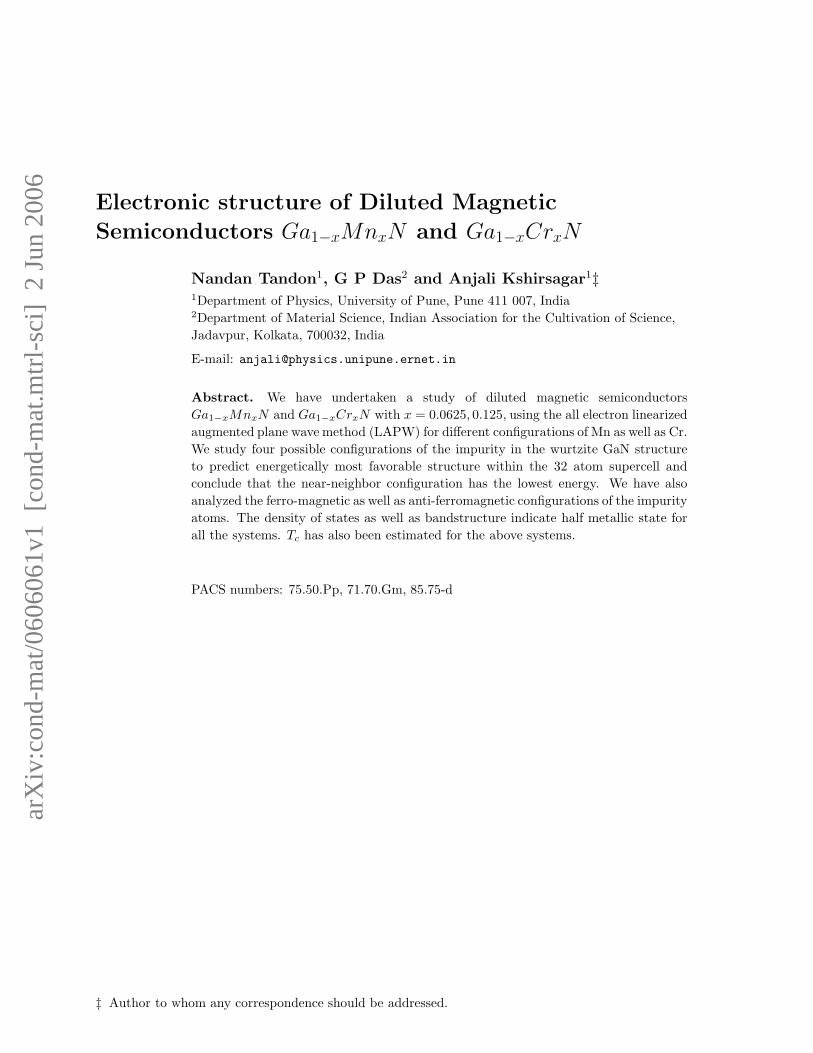
(a) (b)
Figure 1. Mn-projected majority spin (a) dt2 and (b) de bands in Ga15MnN16.
states of substituted Ga, one hole per Mn is introduced into the system. Figure 1 shows
the Mn-projected dt2 and de majority spin electronic structure for Ga15MnN16. The Mn-
d states lie at the top of the valence band and cross the ǫF in some places. These are
split into de and dt2 states, the dt2 level is two thirds filled and the de is almost occupied.

The minority spin levels are empty and lie above the ǫF indicating 100% spin-polarized
states. The Mn induced states lie in the gap region of GaN. The top of the valence band
in GaN is composed of the N-p levels and the unique properties, particularly the half
metallic state of DMS, thus arise from the TM d and host p interactions that couple the
two subsystems.
0.5
1
1.5
2−10 −5 0 5 10
Energy [eV]
dn
0
0.5
1
1.5
2
up
DO
S (
Sta
tes/
eV c
ell)
εF
Mn−Mn=3.19ÅMn−Mn=5.19Å
(a)
0.5
1
1.5
2−10 −5 0 5 10
Energy [eV]
dn
0
0.5
1
1.5
2
up
DO
S (
Sta
tes/
eV c
ell)
εF
Mn−Mn=6.3ÅMn−Mn=6.0Å
(b)
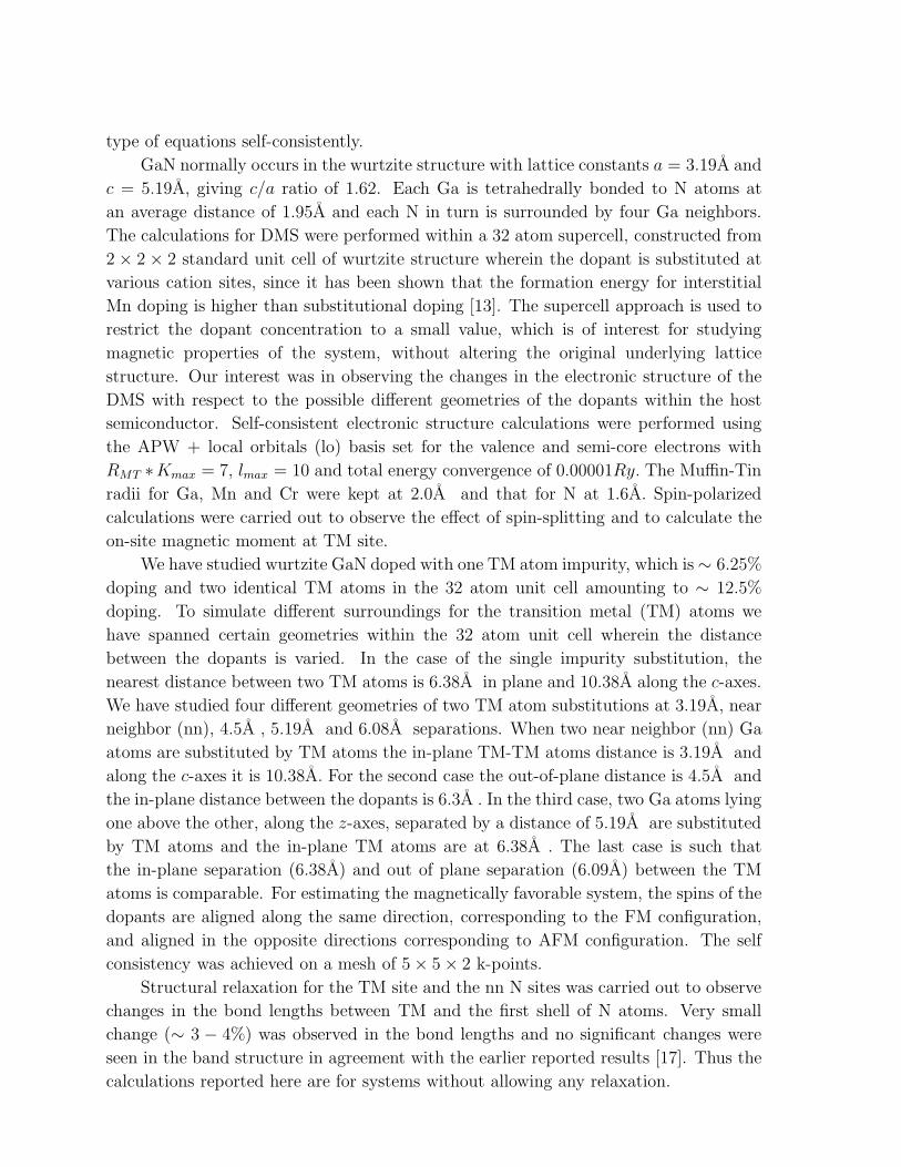
Figure 2. Mn-projected d-DOS in Ga14Mn2N16 (a) with Mn-Mn distance equal to
3.19A and 5.19A and (b) 6.0A and 6.3A. The upper and lower panels represent the
majority and minority spin DOS respectively.
In order to understand the variation of exchange interaction among the TM
impurity with the distance between the TM atoms, the concentration of Mn atoms
was increased to 12.5%, equivalent to introducing 2 Mn atoms in the supercell. Self
consistent calculations were carried out for two different magnetic configurations of Mn
electrons in which the electrons are parallel or antiparallel corresponding to FM or AFM
configuration. For all the geometries of the dopants, systems, as described in section
II, with FM configuration of the Mn atoms were found to have lower energy. Since the
Mn-d levels are responsible for observed half metallic behavior, a comparison of Mn-d
DOS in various geometries is shown in figure 2, (a) for separations 3.19A and 5.2A and
(b) for 6.0A and 6.3A. Here the half metallic state is evident in all the cases. The
TM-TM distance of 6.3A corresponds to single TM doping (6.25%).
The Mn d−DOS is broad for substitution at nn distance. In all the other cases
the band is split indicating that the majority spin d-bands of the two Mn atoms at
nn overlap. On increasing Mn-Mn distance, d-band splitting takes place implying a
reduction in the interaction between the TM atoms. It may be noted that the minority
spin conduction band overlaps with the majority spin band for nn substitution. A gap
of ∼ 0.5eV is present between the minority spin conduction band and majority spin
band for Mn-Mn distance greater than nn. The minority spin valence band as well
as conduction band is far apart from the ǫF thus retaining the highly spin polarized
state also seen in the single Mn doped Ga14MnN16 system. The down spin gap is 2eV
for nn configuration and increases to 2.5eV at larger separations. On increasing the
distance between the Mn atoms, splitting of d-level increases. This is consistent with
the observation that in single impurity doping, TM-TM atom distance is 6.0A and
splitting of the Mn-d band is larger as seen in figure 2(b). The magnetic moment at
Mn-site does not depend on the distance between the dopant atoms and has a value
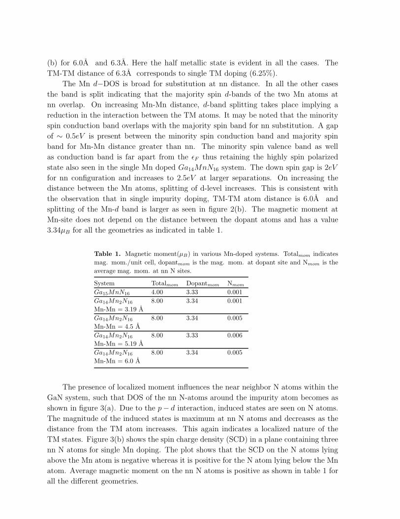
3.34µB for all the geometries as indicated in table 1.
Table 1. Magnetic moment(µB) in various Mn-doped systems. Totalmom indicates
mag. mom./unit cell, dopantmom is the mag. mom. at dopant site and Nmom is the
average mag. mom. at nn N sites.
System Totalmom Dopantmom Nmom
Ga15MnN16 4.00 3.33 0.001
Ga14Mn2N16 8.00 3.34 0.001
Mn-Mn = 3.19 A
Ga14Mn2N16 8.00 3.34 0.005
Mn-Mn = 4.5 A
Ga14Mn2N16 8.00 3.33 0.006
Mn-Mn = 5.19 A
Ga14Mn2N16 8.00 3.34 0.005
Mn-Mn = 6.0 A
The presence of localized moment influences the near neighbor N atoms within the
GaN system, such that DOS of the nn N-atoms around the impurity atom becomes as
shown in figure 3(a). Due to the p− d interaction, induced states are seen on N atoms.
The magnitude of the induced states is maximum at nn N atoms and decreases as the
distance from the TM atom increases. This again indicates a localized nature of the
TM states. Figure 3(b) shows the spin charge density (SCD) in a plane containing three
nn N atoms for single Mn doping. The plot shows that the SCD on the N atoms lying
above the Mn atom is negative whereas it is positive for the N atom lying below the Mn
atom. Average magnetic moment on the nn N atoms is positive as shown in table 1 for
all the different geometries.

0.5
1-5 -4 -3 -2 -1 0 1 2 3 4 5
Energy [eV]
dn
0
0.5
1
up
DO
S (
Sta
tes/
eV c
ell)
εF
(a)
(b)
Figure 3. (a) Variation in partial-DOS at 3 N-sites in Ga15MnN16. The solid lines:
nn-N along c−axis. Dotted lines:nn-N in plane. Dashed-dotted lines: next nn-N (b)
SCD plot in a plane of three nn N atoms.
3.2. Cr doped systems
Electronic structure calculation for substitutional doping of Cr in the GaN system
was also done and is analyzed in a similar fashion. For each Cr doped in the 32
atom supercell, equivalent to 6.25% doping, there are five spin up d-states which are
introduced in the GaN band gap. Since the Cr atom has 4s23d4 valence electrons, only
three of the electron states out of the five 3 − d levels are occupied, thus creating two
hole states per Cr substitution. Single Cr doping into the 32 atom supercell at cation
site results in the Cr-d levels appearing in the band gap of the semiconductor host as
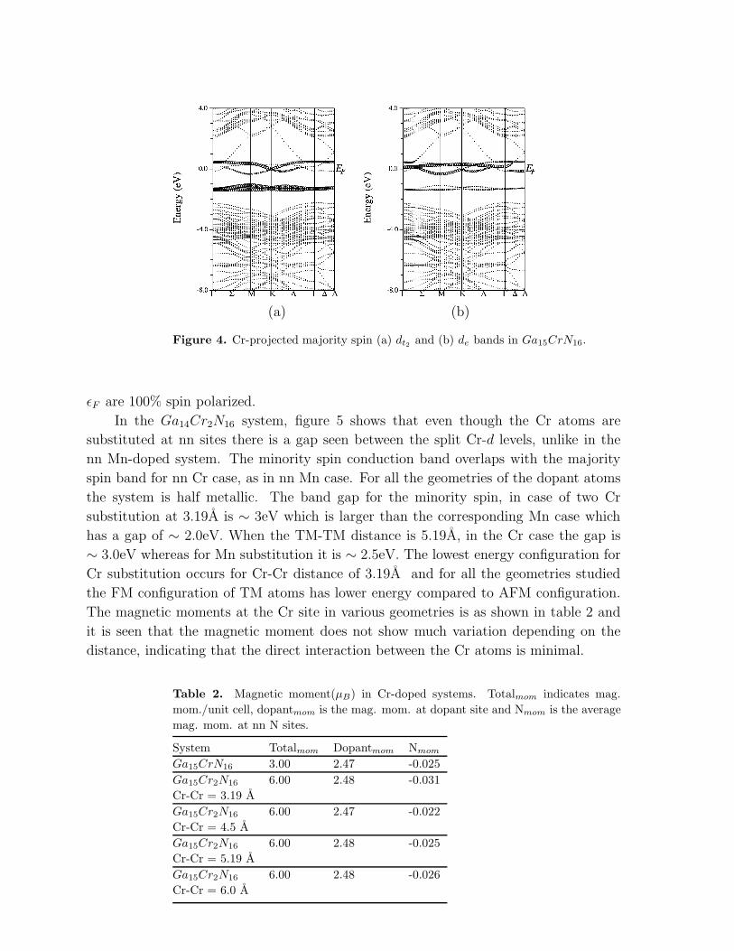
seen in figure 4. The Cr dt2 levels split (figure 4(a)), out of which two energy levels lie
below the Fermi level (ǫF ) and are occupied. The third level which is ∼ 0.5eV above is
unoccupied. One of the de level is occupied and the other lies just above the ǫF as seen
in figure 4(b). However, the hybridization of dt2 and de majority spin states is negligible
and these levels are well separated as opposed to Mn doped case. As in the case of Mn
doping, the Cr minority spin d-states are above the ǫF and so the impurity states at the
(a) (b)
Figure 4. Cr-projected majority spin (a) dt2 and (b) de bands in Ga15CrN16.
ǫF are 100% spin polarized.
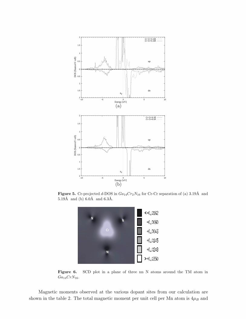
In the Ga14Cr2N16 system, figure 5 shows that even though the Cr atoms are
substituted at nn sites there is a gap seen between the split Cr-d levels, unlike in the
nn Mn-doped system. The minority spin conduction band overlaps with the majority
spin band for nn Cr case, as in nn Mn case. For all the geometries of the dopant atoms
the system is half metallic. The band gap for the minority spin, in case of two Cr
substitution at 3.19A is ∼ 3eV which is larger than the corresponding Mn case which
has a gap of ∼ 2.0eV. When the TM-TM distance is 5.19A, in the Cr case the gap is
∼ 3.0eV whereas for Mn substitution it is ∼ 2.5eV. The lowest energy configuration for
Cr substitution occurs for Cr-Cr distance of 3.19A and for all the geometries studied
the FM configuration of TM atoms has lower energy compared to AFM configuration.
The magnetic moments at the Cr site in various geometries is as shown in table 2 and
it is seen that the magnetic moment does not show much variation depending on the
distance, indicating that the direct interaction between the Cr atoms is minimal.
Table 2. Magnetic moment(µB) in Cr-doped systems. Totalmom indicates mag.
mom./unit cell, dopantmom is the mag. mom. at dopant site and Nmom is the average
mag. mom. at nn N sites.
System Totalmom Dopantmom Nmom
Ga15CrN16 3.00 2.47 -0.025
Ga15Cr2N16 6.00 2.48 -0.031
Cr-Cr = 3.19 A
Ga15Cr2N16 6.00 2.47 -0.022
Cr-Cr = 4.5 A
Ga15Cr2N16 6.00 2.48 -0.025
Cr-Cr = 5.19 A
Ga15Cr2N16 6.00 2.48 -0.026
Cr-Cr = 6.0 A
0.5
1
1.5
2−10 −5 0 5 10
Energy [eV]
dn
0
0.5
1
1.5
2
up
DO
S (
Sta
tes/
eV c
ell)
εF
Cr−Cr=3.19ÅCr−Cr=5.19Å
(a)
0.5
1
1.5
2−10 −5 0 5 10
Energy [eV]
dn
0
0.5
1
1.5
2
up
DO
S (
Sta
tes/
eV c
ell)
εF
Cr−Cr=6.3ÅCr−Cr=6.0Å
(b)
Figure 5. Cr-projected d-DOS in Ga14Cr2N16 for Cr-Cr separation of (a) 3.19A and
5.19A and (b) 6.0A and 6.3A.
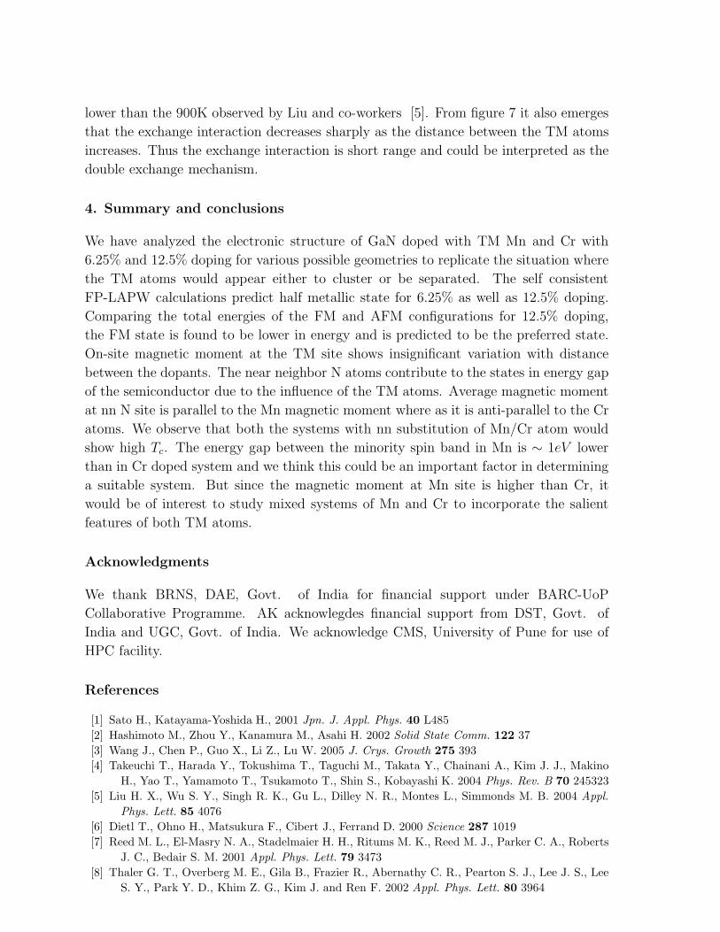
Figure 6. SCD plot in a plane of three nn N atoms around the TM atom in
Ga14CrN16.
Magnetic moments observed at the various dopant sites from our calculation are
shown in the table 2. The total magnetic moment per unit cell per Mn atom is 4µB and

the average magnetic moment on the nn N atoms in case of Mn-doping is parallel to the
Mn-moment. This can be understood as penetration of the spin-polarized Mn states
to the neighboring host which does not have any of its own states in the gap region.
The magnetic moment per unit cell per Cr atom is 3µB. The average magnetic moment
on the nn N atom is anti-parallel to Cr-moment. The difference in the orientation of
the average magnetic moment on nn N atoms of Mn and Cr is due to the difference
in the p DOS of the nn N along the z axis (figure not shown here) compared to the
nn N atoms lying in the xy plane above the TM atoms. There is not much variation
of magnetic moment with increase in Cr-Cr distance and shows a similar trend as Mn
doped systems. The magnitude of average nn-N magnetic moment is greater in case
of Cr substitution, which contribute one less electron to the hybridized valcen band.
SCD in figure 6 on all of the nn-N atoms of the single Cr (only 3 nn N atoms shown in
figure 6) doped system is negative thus showing that the TM atom and the nn-N are
anti-ferromagnetically coupled.
3.3. Estimation of Tc
We have predicted the Tc for the DMS based on Ga16Mn2N16 and Ga16Cr2N16 considering
the mean field approximation. Figure 7 shows the ∆E = EAFM − EFM for the Mn/Cr
0
0.02
0.04
0.06
0.08
0.1
0.12
0.14
0.16
0.18
0.2
3 3.5 4 4.5 5 5.5 6 6.5 7
Distance (Å)
Ene
rgy
[eV
]
Mn
Cr
75
240
405
570
735
900
3 3.5 4 4.5 5 5.5 6 6.5
Distance (Å)
Mn
Cr
Tc
[K]
Figure 7. ∆E = EAFM − EFM for Mn and Cr doping. Inset shows the mean field
Tc variation with distance between dopants.
doped systems, where EAFM is the total energy for the antiferromagnetic (AFM)
configuration and EFM is the total energy for the ferromagnetic (FM) configuration.
Observed variation ∆E vs distance for Mn substituted DMS agrees with the one reported
by Sanyal [13]. ∆E is a measure of the exchange interaction in the system. Highest ∆E
is seen for the case where the TM atoms are substituted as near neighbors, signifying
larger overlap of the magnetic impurity orbitals. For Mn doping at nn ∆E ∼ 0.14eV,
this compares well with the value calculated for dimer substitution by Uspenskii et.
al [12] which compared qualitatively with the high Tc = 940K measured [9]. As for
the identical Cr case ∆E ∼ 0.16eV also compares well with the observed Tc but is
lower than the 900K observed by Liu and co-workers [5]. From figure 7 it also emerges
that the exchange interaction decreases sharply as the distance between the TM atoms
increases. Thus the exchange interaction is short range and could be interpreted as the
double exchange mechanism.
4. Summary and conclusions
We have analyzed the electronic structure of GaN doped with TM Mn and Cr with
6.25% and 12.5% doping for various possible geometries to replicate the situation where
the TM atoms would appear either to cluster or be separated. The self consistent
FP-LAPW calculations predict half metallic state for 6.25% as well as 12.5% doping.
Comparing the total energies of the FM and AFM configurations for 12.5% doping,
the FM state is found to be lower in energy and is predicted to be the preferred state.
On-site magnetic moment at the TM site shows insignificant variation with distance
between the dopants. The near neighbor N atoms contribute to the states in energy gap
of the semiconductor due to the influence of the TM atoms. Average magnetic moment
at nn N site is parallel to the Mn magnetic moment where as it is anti-parallel to the Cr
atoms. We observe that both the systems with nn substitution of Mn/Cr atom would
show high Tc. The energy gap between the minority spin band in Mn is ∼ 1eV lower
than in Cr doped system and we think this could be an important factor in determining
a suitable system. But since the magnetic moment at Mn site is higher than Cr, it
would be of interest to study mixed systems of Mn and Cr to incorporate the salient
features of both TM atoms.
Acknowledgments
We thank BRNS, DAE, Govt. of India for financial support under BARC-UoP
Collaborative Programme. AK acknowlegdes financial support from DST, Govt. of
India and UGC, Govt. of India. We acknowledge CMS, University of Pune for use of
HPC facility.
References
[1] Sato H., Katayama-Yoshida H., 2001 Jpn. J. Appl. Phys. 40 L485
[2] Hashimoto M., Zhou Y., Kanamura M., Asahi H. 2002 Solid State Comm. 122 37
[3] Wang J., Chen P., Guo X., Li Z., Lu W. 2005 J. Crys. Growth 275 393
[4] Takeuchi T., Harada Y., Tokushima T., Taguchi M., Takata Y., Chainani A., Kim J. J., Makino
H., Yao T., Yamamoto T., Tsukamoto T., Shin S., Kobayashi K. 2004 Phys. Rev. B 70 245323
[5] Liu H. X., Wu S. Y., Singh R. K., Gu L., Dilley N. R., Montes L., Simmonds M. B. 2004 Appl.
Phys. Lett. 85 4076
[6] Dietl T., Ohno H., Matsukura F., Cibert J., Ferrand D. 2000 Science 287 1019
[7] Reed M. L., El-Masry N. A., Stadelmaier H. H., Ritums M. K., Reed M. J., Parker C. A., Roberts
J. C., Bedair S. M. 2001 Appl. Phys. Lett. 79 3473
[8] Thaler G. T., Overberg M. E., Gila B., Frazier R., Abernathy C. R., Pearton S. J., Lee J. S., Lee
S. Y., Park Y. D., Khim Z. G., Kim J. and Ren F. 2002 Appl. Phys. Lett. 80 3964
[9] Sonoda S., Shimizu S., Sasaki T., Yamamoto Y. and Hori H. 2002 J. Cryst. Growth 237-239 1358
[10] Ando K., 2003 Appl. Phys. Lett. 82 100
[11] Zajac M., Gosk J., Kaminska M., Twardowski A., Szyszko T. and Podsiadlo S. 2001 Appl. Phys.
Lett. 79 2432
[12] Uspenskii Y., E. Kulatov, H. Mariette, H. Nakayama, H. Ohta J. Magn. Magn. Mater. 258-259,
248-250 (2003).
[13] Sanyal B. and Mirbt S. 2005 J. M. M. M. 290-291 1408
[14] Raibiger H., Ayuela A. and Nieminen R. M. 2004 J. Phys. Condens. Matter 16 L457-L462
[15] P. Blaha, K. Schwarz, G. K. H. Madsen, D. Kvasnicka and J. Luitz, An augmented plane wave
plus local orbitals program for calculating crystal properties, Vienna Univ. of Technology, Austria
(2001) ISBN 3-950131-1-2
[16] Perdew J. P., Burke K. and Ernzerhof M. 1996 Phys. Rev. Lett. 77 3865
[17] Kronik L., Jain M. and Chelikowsky R. 2002 Phys. Rev. B 66 041203
[18] Das G. P., Rao B. K. and Jena P. 2003 Phys. Rev. B 68, 35207
[19] Das G. P., Rao B. K. and Jena P. 2004 Phys. Rev. B 69, 214422


![Growth model for plasma-assisted molecular beam epitaxy of N-polar and Ga-polar In[sub x]Ga[sub 1-x]N](https://static.fdokumen.com/doc/165x107/6316ef5b0f5bd76c2f02b44a/growth-model-for-plasma-assisted-molecular-beam-epitaxy-of-n-polar-and-ga-polar.jpg)