Electron spin for classical information processing: a brief survey of spin-based logic devices,...
130
1 Electron Spin for Classical Information Processing: A Brief Survey of Spin-Based Logic Devices, Gates and Circuits Supriyo Bandyopadhyay 1,† and Marc Cahay * † Department of Electrical and Computer Engineering Virginia Commonwealth University Richmond, VA 23284, USA * Department of Electrical and Computer Engineering University of Cincinnati Cincinnati, OH 45221, USA ABSTRACT In electronics, information has been traditionally stored, processed and communicated using an electron’s charge. This paradigm is increasingly turning out to be energy-inefficient, because movement of charge within an information-processing device invariably causes current flow and an associated dissipation. Replacing “charge” with the “spin” of an electron to encode information may eliminate much of this dissipation and lead to more energy-efficient “green electronics”. This realization has spurred significant research in spintronic devices and circuits where spin either directly acts as the physical variable for hosting information or augments the role of charge. In this review article, we discuss and elucidate some of these ideas, and highlight 1 Corresponding author. E-mail: [email protected]
Transcript of Electron spin for classical information processing: a brief survey of spin-based logic devices,...

1
Electron Spin for Classical Information Processing: A Brief Survey of Spin-Based Logic
Devices, Gates and Circuits
Supriyo Bandyopadhyay1,† and Marc Cahay*
†Department of Electrical and Computer Engineering
Virginia Commonwealth University
Richmond, VA 23284, USA
*Department of Electrical and Computer Engineering
University of Cincinnati
Cincinnati, OH 45221, USA
ABSTRACT
In electronics, information has been traditionally stored, processed and communicated using
an electron’s charge. This paradigm is increasingly turning out to be energy-inefficient, because
movement of charge within an information-processing device invariably causes current flow and
an associated dissipation. Replacing “charge” with the “spin” of an electron to encode
information may eliminate much of this dissipation and lead to more energy-efficient “green
electronics”. This realization has spurred significant research in spintronic devices and circuits
where spin either directly acts as the physical variable for hosting information or augments the
role of charge. In this review article, we discuss and elucidate some of these ideas, and highlight 1 Corresponding author. E-mail: [email protected]

2
their strengths and weaknesses. Many of them can potentially reduce energy dissipation
significantly, but unfortunately are error-prone and unreliable. Moreover, there are serious
obstacles to their technological implementation that may be difficult to overcome in the near
term.
This review addresses three constructs: (1) single devices or binary switches that can be
constituents of Boolean logic gates for digital information processing, (2) complete gates that are
capable of performing specific Boolean logic operations, and (3) combinational circuits or
architectures (equivalent to many gates working in unison) that are capable of performing
universal computation.

3
TABLE OF CONTENTS
1. INTRODUCTION………………………………………………………………………...6
2. SPIN BASED TRANSISTORS AND LOGIC SWITCHES………………………….......8
2.1. The Spin Field Effect Transistor (SPINFET)…………………………………….9
2.1.1. The bane of spin injection efficiency………………………….......15
2.1.2. Other types of SPINFETs………………………………………....17
2.1.3. Is the SPINFET any more energy-efficient than the traditional
MISFET?....................................................................................................17
2.1.4. Analog applications of the SPINFET………………………..........19
2.1.5. Experimental status of the SPINFET……………………………...21
2.1.6. Obstacles to experimental realization of SPINFETS………….......22
2.2. Other Types of Spin Based Transistors…………………………………………24
2.2.1. The transit time spin field effect transistor (TTSFET)……………24
2.2.2. Is the TTSFET an energy-efficient device?.....................................27
2.2.3. Experimental status of the TTSFET……………………………....28
2.3. Comparison Between the SPINFET, TTSFET and MISFET for Device
Density, Speed and Cost……………………………………………………………..29
2.4. Spin Bipolar Junction Transistor………………………………………………..29
3. SPIN BASED LOGIC GATES………………………………………………………….32
3.1. A Magnetic Tunnel Junction (MTJ) Switch…………………………………….33
3.2. A Reconfigurable Magnetic Tunnel Junction Logic Gate………………………35
3.2.1. Speed, energy-efficiency and cost of MTJ logic gates…………..37

4
4. SPIN BASED LOGIC ARHCITECTURES AND CIRCUITS FOR COMPUTATION..38
4.1. Single Spintronics: An Energy-Efficient Paradigm……………………………..38
4.2. The Single Spin Logic (SSL) Family……………………………………………42
4.2.1. The SSL NAND gate and spin wire……………………………...44
4.2.2. Unidirectional signal transfer along a spin wire…………………49
4.2.3. Energy dissipation in SSL………………………………………..51
4.2.4. The speed of SSL………………………………………………...53
4.2.5. The gate error probability in SSL………………………………..57
4.2.6. The temperature of operation of SSL……………………………58
4.2.7. Current experimental status of SSL……………………………...59
4.2.8. Organic molecules for SSL?..........................................................60
4.3. Extending SSL to Room Temperature Operation: Replacing a Single Spin With a
Collection of Spins……………………………………………………………….61
4.3.1. Magnetic quantum cellular automata (MQCA) logic gates……...64
4.3.2. Magnetic quantum cellular automata (MQCA) circuits…………68
4.3.3. Unidirectional signal propagation in MQCA circuits : Granular and
global clocks……………………………………………………..70
4.3.4. Global clocking in MQCA leads to non-pipelined architecture…73
4.3.5. The bit error probability in MQCA with global clock and granular
clock……………………………………………………………...75
4.3.6. The “misalignment” problem associated with the use of a vector
(magnetic field) as the clock in MQCA circuits…………………75
4.3.7. Experimental status of MQCA…………………………………..77

5
4.3.8. Reading and writing of bits in MQCA and associated power
dissipation………………………………………………………..78
4.4. Domain Wall Logic……………………………………………………………..79
4.4.1. Writing and reading of binary data in domain wall logic………..80
4.4.2. The misalignment problem in domain wall logic………………..81
4.4.3. Experimental status of magnetic domain wall logic……………..81
5. SPIN ACCUMULATION LOGIC………………………………………………………82
5.1. The Logic Separation Between Bits 0 and 1 in SAL……………………………83
5.2. Energy Dissipation in SAL Logic Gates………………………………………...84
6. SPIN WAVE BUS (SWB) TECHNOLOGY……………………………………………85
6.1.Is the SWB Technology Energy-Efficient?...........................................................87
6.2. Experimental Status of the SWB Technology…………………………………..88
6.3. Shortcomings of the SWB Technology…………………………………………88
7. CONCLUSION…………………………………………………………………………..91

6
1. INTRODUCTION
The workhorse of modern digital electronics is the celebrated “transistor” discovered by
Bardeen, Brattain and Shockley more than sixty years ago. The transistor is a quintessential
charge based device where an electron’s charge is utilized to encode information in digital form.
This is most evident in the case of the metal-insulator-semiconductor-field-effect-transistor
(MISFET), which has three terminals: the source, the drain and the gate. When a positive
potential is applied on the gate terminal that sits between the source and the drain, it attracts
negatively charged electrons into the channel region separating the source and the drain. The
incoming electrons make the channel conducting and allow current to flow between the source
and drain. This is the ON state of the transistor. If we reverse the polarity of the gate potential,
then electrons are repelled from the channel by the negative charge on the gate terminal, which
makes the channel non-conducting and drops the device conductance dramatically (usually by ~
6 orders of magnitude). This turns the transistor OFF. The two conductance states - ON and OFF
– are used to encode the binary bits 0 and 1, which, in turn, allows one to store and process
digital information using binary bit streams.
The problem with this strategy is that switching between the ON and OFF states always
requires moving an amount of charge Q in and out of the channel, which needs an amount of
energy equal to QΔV, where ΔV is the change in the gate potential necessary to change the
channel charge by the quantity Q. This energy is dissipated as heat when the switching action is
over.
Heat dissipation is a serious spoiler in modern integrated circuits. Today’s transistors
dissipate between 1,500 and 2,500 eV (0.24-0.4 fJ) of energy when they switch from the ON to

7
the OFF state, or vice versa [1]. The Pentium IV chip has a transistor density of 108 cm-2 and
with a 2.8 GHz clock should dissipate between 2.4×10-16×108×2.8×109 = 67 Watts/cm2 and 4×10-
16×108×2.8×109 = 112 Watts/cm2 if all the transistors switch simultaneously. With a 5% activity
level, i.e. if only one in twenty transistors switch at any given time, the power dissipation should
be between 3.35 and 5.6 Watts/cm2. In actuality, the Pentium IV chip, which has an area of 13
cm2 (Northwood generation), dissipates about 50 Watts [2], which translates to a power
dissipation of 3.8 Watts/cm2. This level of power dissipation is not particularly worrisome since
removal of 1000 Watts/cm2 from a chip using conventional technology was demonstrated almost
30 years ago [3].
The chip making industry however is driven by an empirical law known as Moore’s law [4]
that mandates doubling of the transistor density on a chip every 18 months or so. If Moore’s law
holds in perpetuity, we should reach a transistor density of ~ 1013 cm-2 by 2025, given that the
Pentium IV chip was released in ca. 2000. Furthermore, if the clock speed increases to 10 GHz
by then, the power dissipation on a chip will reach 2 MW/cm2 (still with 5% activity level)
unless we can reduce the energy dissipation in a transistor during switching. The thermal load
associated with a heat dissipation of 2 MW/cm2 approaches that in a rocket nozzle. Therefore,
unless revolutionary new heat sinking technologies are pressed into service, thermal management
on a chip will inevitably fail and continued miniaturization of transistors in accordance with
Moore’s law should stop well before 2025. The International Technology Roadmap for
Semiconductors has termed this impending catastrophe the “Red Brick Wall” [1].
As long as we use charge to encode information, we will always be menaced by the Red
Brick Wall since charge based electronics is intrinsically energy-inefficient and dissipative. This
is due to the fact that charge is a scalar quantity which has only magnitude and no direction or

8
any other attribute. Therefore, if we intend to encode binary bit information in charge, then we
must do so by using two different magnitudes or amounts of charge – Q1 and Q2 – to represent
the two bits. We cannot use anything else, other than a difference in the magnitude, to demarcate
the logic levels. If that is the case, then switching will always dissipate an amount of energy
equal to ( )1 2V Q QΔ − , which is never zero since 1 2Q Q≠ . In fact, we would prefer to make Q1
very different from Q2 so that the logic bits are well-separated and clearly distinguishable from
each other in a noisy environment, which will reduce the error associated with mistaking one for
the other. Thus, there is a fundamental connection between dissipation and bit error probability.
Increasing one reduces the other and vice versa. This fundamental truism is enshrined in the
famous Landauer-Shannon result for the ultimate limits on dissipation that we will have occasion
to discuss later in this article.
2. SPIN BASED TRANSISTORS AND LOGIC SWITCHES
Since the fundamental source of dissipation in all charge based transistors is charge motion
within the device mandated by the requirement that 1 2Q Q≠ , it is natural to seek ways where the
switching action of the transistor, i.e. switching from a high conductance state to a low
conductance state (or vice versa), can be accomplished without changing the amount of charge in
the device. In other words, we wish to switch between two well distinguished logic levels while
maintaining 1 2Q Q= . To our knowledge, the first proposal that found a route to realizing this
objective is that of the celebrated Spin Field Effect Transistor (SPINFET) where the spin degree
of freedom of an electron is utilized to switch the conductance of a MISFET-like structure from

9
high to low, or vice versa, without changing the amount of charge in the channel. We describe
this device next.
2.1. The Spin Field Effect Transistor (SPINFET)
In a seminal paper published in 1990 [5], Datta and Das proposed a remarkable idea for
changing the conductance of a MISFET-like device without changing the channel charge at all.
The way they accomplished this was to use the spin degree of freedom of channel electrons,
instead of the charge degree of freedom, to switch the channel conductance. Their device, which
has since been dubbed a SPINFET (Spin Field Effect Transistor), has the exact same physical
structure as a traditional MISFET, except that the source and drain contacts are ideal (half-
metallic) ferromagnets that are magnetized in the direction of current flow in the channel. We
call this the “parallel configuration” since both contacts are magnetized in the same direction, i.e.
the north pole of the source magnet faces the south pole of the drain magnet, or vice versa. This
device is represented schematically in Fig. 1.
The SPINFET has been discussed in many papers dealing with spintronics since it truly
inspired the entire field. Here, we will describe its operation by invoking only classical physics
since there is a misperception among some that it relies on quantum mechanical interference
between two orthogonal spin states, and is therefore a quantum interference device. That is not
correct. Although, in ref. [5], Datta and Das described their device in a language that might
convey this impression, in reality this device is purely classical and its operation can be
described classically. That should be welcome news since quantum interference devices are very
delicate [6, 7], and while they certainly have a role as laboratory curiosities, they are unlikely to
10
be practical as operating devices in a circuit environment. The Datta-Das device, if ever realized,
will actually be quite robust because it is classical.
To keep the ensuing discussion focused on the essential elements, we will assume that the
channel of the SPINFET in Fig. 1 is a strictly one-dimensional quantum wire. A one-dimensional
channel performs better than the more conventional two-dimensional channel for many reasons.
First, the two dimensional device can never be turned off completely, even in the ideal case,
because the effect of the gate potential on the spin of an electron in the channel depends on the
direction of the electron’s velocity [5]. In a two-dimensional channel, the electron’s velocity
spans two dimensions, so that even when the current is shut off completely for electrons with
velocity along one direction, it is not shut off for electrons whose velocities have non-zero
components in the orthogonal direction. Hence, a transistor with a two-dimensional channel will
invariably have a significant leakage current flowing in the OFF state. In contrast, electrons in a
one-dimensional channel have their velocity vectors always pointing along one direction only.
Such a transistor can be completely turned off (provided everything else is ideal), resulting in
zero leakage current. A second reason for preferring a one-dimensional channel is that the
SPINFET works best if there is no random spin relaxation in the channel. In semiconductor
channels, random spin relaxation usually occurs via two modes: the D’yakonov-Perel’ mode [8]
and the Elliott-Yafet mode [9]. The former is completely suppressed in a one-dimensional
channel [10-12] and the latter is also significantly reduced by one-dimensional confinement.
Therefore, the one-dimensional device is not just a convenient idealization, it actually happens to
be the ideal prototype.
We will now make three assumptions that will allow us to describe the SPINFET’s operation
lucidly.

11
• First, the ideal half-metallic ferromagnetic source contact is assumed to be a perfect
spin injector that injects only its majority spin, at the complete exclusion of its
minority spin. Similarly, the half-metallic ferromagnetic drain contact is assumed to
be an ideal spin detector (or transmitter) that transmits only its own majority spin and
completely blocks its minority spin. In other words, the spin injection and detection
efficiencies at the source and drain respectively, defined as
min
min
majS D
maj
I II I
ξ ξ−
= =+
, (1)
are both 100%. Here majI is the injected or detected current due to electrons with the
majority spin and minI is that due to electrons with the minority spin.
• Second, we will assume that the ferromagnetic contacts do not cause any magnetic
field in the channel. A magnetic field can cause “spin mixing” in the channel that has
deleterious effects which will adversely affect the transistor’s operation [13, 14].
• Finally, we will assume that there is no random spin relaxation in the channel, i.e.
neither the D’yakonov-Perel’ nor the Elliott-Yafet mechanism (nor any other spin
relaxing mechanism for that matter) is operative. There can be plenty of scattering in
the channel due to phonons, other electrons or holes, and non-magnetic impurities,
but they should not relax spin.
As shown in Fig. 1, the source and drain contacts are magnetized in the +z direction so that
the majority spins in both contacts are polarized in the +z-direction. Hence all spins injected
from the source into the channel under a source-to-drain bias are initially polarized in the +z-
direction. This is also the direction of current flow or electron velocity in the channel.

12
Without any gate voltage, the injected spins arrive at the drain with their polarizations intact
and transmit completely through the drain contact (since the majority spin in the source is also
majority spin in the gate), resulting in maximum channel current. When the gate voltage is
turned on, it causes an electric field to appear in the +y-direction. This electric field induces a
Rashba spin-orbit interaction [15] in the channel which gives rise to an effective magnetic field
in the direction mutually perpendicular to the electron velocity and the electric field, i.e. in the
+x-direction. The flux density of this field is [16]
*
462 ˆ,Rashba y zB
m aB v xgμ
⎡ ⎤= Ε⎢ ⎥
⎣ ⎦
r
h (2)
where *m is the effective mass of electrons in the channel, a46 is a material constant indicative of
the strength of the Rashba spin-orbit interaction in the channel material, yΕ is the electric field in
the y-direction induced by the applied gate voltage, zv is the z-directed velocity of electrons in
the channel and x̂ is the unit vector in the x-direction.
Because we assumed 100% spin injection efficiency, the source injects electrons into the
channel with their spins polarized exclusively in the +z-direction. The x-directed magnetic
field RashbaBr
, caused by the gate potential, will make these spins precess about RashbaBr
in the y-z
plane (Larmor precession) as they travel towards the drain. The angular frequency of this spin
precession is given by the Larmor formula:
*
462
2B Rashbay z
g B a md vdt
μφΩ = = = Ε
h h (3)
and therefore the corresponding spatial rate of precession is
*
462
2y
z
a md d dzdt dtdz v
φ φ Ω= = = Ε
h. (4)

13
Note from the last equation that the spatial rate of precession is independent of the
electron velocity and therefore is the same for every electron, regardless of its velocity or kinetic
energy. Consequently, every electron precesses by exactly the same angle in traversing the
channel. A scattering event due to a phonon or impurity in the channel can change an electron’s
velocity and scatter it backwards, but as long as it reverses direction once again (owing to
another scattering event or because of the electrostatic potential gradient between the source and
drain) and finally arrives at the drain, its spin would have precessed by exactly the same angle as
every other electron that traversed the channel, irrespective of its scattering history! Thus, the
angle by which every spin precesses as it travels from the source to the drain is constant and
given by
*
462
2y
a m LΦ = Εh
, (5)
where L is the channel length (distance between source and drain). Note, once again, that as long
as the channel is one-dimensional, transport in the SPINFET channel does not have to be ballistic
to keep Φ constant. There can be frequent scattering in the channel, but as long as these
scattering events conserve spin,Φ will be the same for every electron.
Using the so-called Bloch sphere concept [16], and noting that every electron entered the
channel with +z-polarized spin, the 2×1 component spinor that represents the spin of any
arbitrary electron arriving at the drain contact can be written as
[ ]cos
2
sin2
idrain
i
ee
γ
ϕ
ψ
⎡ Φ ⎤⎛ ⎞⎜ ⎟⎢ ⎥⎝ ⎠⎢ ⎥=
⎢ ⎥Φ⎛ ⎞⎢ ⎥⎜ ⎟
⎝ ⎠⎣ ⎦
, (6)
where ν and ϕ are two arbitrary phase angles and Φ is the spin precession angle given in
Equation (5).

14
The probability amplitude for this arriving spin to transmit through the drain (whose majority
spins are +z-polarized and hence described by the spinor1
0
⎡ ⎤⎢ ⎥⎢ ⎥⎢ ⎥⎣ ⎦
) is given by
1
cos sin cos02 2 2
i i it e e eγ ϕ γ− − −⎡ ⎤⎡ Φ Φ ⎤ Φ⎛ ⎞ ⎛ ⎞ ⎛ ⎞= =⎜ ⎟ ⎜ ⎟ ⎜ ⎟⎢ ⎥⎢ ⎥⎝ ⎠ ⎝ ⎠ ⎝ ⎠⎣ ⎦ ⎣ ⎦. (7)
Note that this transmission amplitude t is the same for every electron since every one of them
entered the channel with the same spin orientation (+z) from the source and rotated by the same
angle by the time it arrived at the drain. Therefore Φ and consequently t is the same for every
electron.
The current through a one-dimensional conductor subjected to a bias of biasV is given by the
Tsu-Esaki formula [17] ( ) ( ) ( )2
0
2F bias F
eI dE t E f E E f E eV Eh
∞
= − − + −⎡ ⎤⎣ ⎦∫ 2, where EF is the
Fermi energy in the injecting contact. Therefore, the source-to-drain current in a SPINFET with
one-dimensional channel subjected to a source-to-drain bias of SDV is given by
( ) ( ) ( )
( ) ( )
( ) ( )
0
0
2
0
2
0
2
0
2
2 cos2
2cos (since is energy-inde2
SD F SD F
F SD F
I
F SD F
I
eI dE t E f E E f E eV Eh
e dE f E E f E eV Eh
e dE f E E f E eV Eh
∞
∞
∞
= − − + −⎡ ⎤⎣ ⎦
⎧ ⎫Φ⎛ ⎞= − − + −⎡ ⎤⎨ ⎬⎜ ⎟ ⎣ ⎦⎝ ⎠⎩ ⎭
⎧ ⎫Φ⎛ ⎞= − − + − Φ⎡ ⎤⎨ ⎬⎜ ⎟ ⎣ ⎦⎝ ⎠ ⎩ ⎭
∫
∫
∫
14444444444244444444443
1444444442444444443
20
pendent)
cos .2
I Φ⎛ ⎞= ⎜ ⎟⎝ ⎠
(8)
2 This result is strictly valid when there is no inelastic scattering in the channel. Hence we are assuming the absence
of inelastic scattering processes. Elastic scattering processes can be present.

15
where ( ) ( )0
0
2F SD F
eI dE f E E f E eV E
h
∞
⎡ ⎤= − − + −⎣ ⎦∫ .
The above relation clearly shows that the source-to-drain current is maximum when the gate
voltage (or, equivalently, the gate induced electric field yΕ ) is such that Φ is an even multiple of
π, and it falls to zero when the gate voltage is such that Φ is an odd multiple of π. Since Φ
depends on Ey (see Equation (5)), therefore, by changing the gate voltage (and hence Ey), one can
modulate the channel current and realize transistor action. Basically, we can change the current
from maximum to zero and vice versa, i.e. turn the transistor ON and OFF with the gate voltage,
by rotating the spin orientation of channel electrons without having to change their number or
concentration. This is the basic principle of the SPINFET, whose ideal transfer characteristic
(channel current versus gate voltage) is schematically depicted in Fig. 2.
2.1.1. The bane of spin injection efficiency
Fig. 2 and Equation (8) seem to indicate that the ratio of the ON-to-OFF conductance, which
is also the ratio of the ON-current to OFF-current at a fixed source-to-drain bias, will be infinity
since the OFF-current (corresponding to ( )2 1n πΦ = + ) is zero3. In reality, this can be true only
if the source spin injection efficiency and the drain spin detection efficiency are both 100%, i.e.
the source injects only +z-polarized spins and the drain also transmits only +z-polarized spins, at
the complete exclusion of –z-polarized spins. This is what we had tacitly assumed in deriving
Equation (8). However, if either efficiency is less than 100%, then –z-polarized spins will also be
injected by the source and/or transmitted by the drain, which will degrade the on-to-off
3 The reader should appreciate that the OFF-current is zero only because Φ is energy-independent.

16
conductance ratio. It has been shown [16, 18] that when the non-ideality of spin injection and
detection is taken into account, the maximum conductance ratio is given by
11
ON ON S D
OFF OFF S D
G IG I
ξ ξηξ ξ
+= = =
−, (9)
where Sξ and Dξ are the source injection and drain detection efficiencies, respectively. This ratio
becomes infinity only when 1S Dξ ξ= = and decreases rapidly with falling Sξ and Dξ . Obviously,
in order to achieve a conductance on-off ratio of at least 105, typical of today’s transistors, these
injection and detection efficiencies will have to be as high as 99.9995%, which is clearly
impractical (at least at room temperature) given that the maximum spin injection efficiency
demonstrated at a ferromagnetic/semiconductor junction to date is only ~ 70% [19], which would
make the conductance on-off ratio η a paltry 2.9. That is clearly inadequate for any mainstream
application. In the near term, it is unlikely that spin injection and detection efficiencies of
99.9995% can be achieved at room temperature, which means that: (1) the conductance ratio will
remain small, and (2) the leakage current during the OFF state will be large. The former leads to
a large bit error probability (since the ON and OFF states will not be all that distinguishable in a
noisy environment if the conductance ratio is small) and the latter leads to unacceptable standby
power dissipation in a circuit (the transistor will continuously dissipate energy since it is flowing
current even when it is OFF). Ultimately, the poor spin injection and detection efficiencies are
the show-stopper; they will make the SPINFET energy-inefficient and error-prone (i.e.
unreliable), even if this device could be built.
In Fig. 3, we plot the conductance on-off ratio as a function of the spin injection or detection
efficiency, assuming that the two efficiencies are equal. The ratio drops off precipitously with
decreasing efficiency and drops to ~ 10 when the injection or detection efficiency reaches 90%,

17
which is a rather high efficiency yet to be achieved at room temperature. Therefore, the
conductance on-off ratio of the SPINFET is likely to remain low in the near term, which
translates to high bit error rate and large standby power dissipation – both undesirable traits.
2.1.2. Other types of SPINFETs
A number of modifications of the original Datta-Das idea have appeared in the literature over
the last decade. All of them share the property that they switch conductance ON and OFF by
modulating spin instead of channel charge concentration. One replaces the Rashba interaction in
the channel with the Dresselhaus spin-orbit interaction with everything else the same [20],
another uses a delicate balance between the Rashba and Dresselhaus interactions [21, 22], and a
third relies on inducing spin relaxation in the channel with a gate voltage [23] to switch between
ON and OFF states. None of these ideas engender any improvement in the conductance on-off
ratio since all of them still require ideal spin injection and detection at ferromagnet/channel
interfaces. Therefore, they all have too low a conductance ON/OFF ratio to be of much use.
None of them is any more energy-efficient than the original Datta-Das device, either.
2.1.3. Is the SPINFET any more energy efficient than the traditional MISFET?
Let us put aside the issue of conductance on-off ratio for the time being and investigate if it
had not been a problem, would the SPINFET been competitive with the traditional MISFET. It
would have been competitive if it consumed less energy when it switched ON or OFF. Since the
SPINFET switches without requiring a change in the electron concentration in the channel, it
18
may at first appear to be more energy-efficient than the MISFET because ( )1 2 0V Q QΔ − = .
However, in reality, it is not. First of all, it should be recognized that there is still charge flowing
through the channel of the SPINFET in the ON state since there is a source-to-drain current. This
causes dissipation just as it does in a traditional MISFET. Therefore, there is no advantage as far
as static power dissipation (during the ON state) is concerned. During the OFF state, the
SPINFET actually has much more static power dissipation if we consider the fact that it has a
much larger leakage current than a MISFET because of the poor conductance ON/OFF ratio.
Finally, if we consider the dynamic power that is dissipated during switching, then the winner is
determined by which device – the SPINFET or the MISFET – requires a smaller turn-on or turn-
off voltage. The turn-on voltage is the potential applied at the gate to turn the device ON (if the
device is normally OFF) while the turn-off voltage is the gate potential required to turn the
device OFF (if it is normally ON). These potentials cause charge movement somewhere in the
circuit and the associated energy dissipation is almost always ~ 2G GC V , where GC is the gate
capacitance and VG is the turn-on (or turn-off) voltage. Assuming that CG is the same for the
MISFET and the SPINFET, since it is determined by structural parameters, what finally
determines the winner among them is VG.
Refs. [18] and [24] have carried out detailed comparisons between the turn-on or turn-off
voltages of a SPINFET and a traditional MISFET. It should be obvious from Equation (5) that
the gate electric field required to turn a SPINFET off is 2
*462
offy a m L
πΕ =
h (corresponding to πΦ = )
so that the turn-off voltage will depend on the channel length L. Longer-channel devices require
a smaller turn-off voltage and therefore are more energy-efficient. Refs. [18] and [24] concluded
that the turn-off voltage of a SPINFET with reasonable channel length (smaller than 100 nm), is

19
actually much larger than that of a comparable normally-on MISFET, primarily because the
strength of Rashba spin-orbit interaction (denoted by the quantity a46) is usually too small in the
conduction band of technologically important semiconductors to make offyΕ small enough to yield
a small turn-off voltage in a short channel device of length ≤100 nm. Only a SPINFET with a
channel length larger than a few μm could be more energy efficient than a MISFET. Such large
devices are no longer practical or affordable. Therefore, the SPINFET does not make a better
digital switch and hence is not particularly desirable for digital information processing.
2.1.4. Analog applications of the SPINFET
If the SPINFET would not yield any significant advantage in digital electronics, does it have
a role to play in analog electronics? Unfortunately, the answer again is no. For analog
applications, the two most important metrics are power gain and bandwidth. Both are determined
by the transconductance of the transistor. Ref. [16] showed that the maximum transconductance
of SPINFET with a one-dimensional channel is
*2
462
2 sin ,im SD S D
s
m ae Lg Vh d
κξ ξκ
= Φh
(10)
where iκ and sκ are the dielectric constants of the gate insulator and semiconductor channel,
respectively, and d is the width of the gate insulator layer (see Fig. 1).
In the common-source or common-gate configurations, a single stage transistor amplifier has
a voltage gain given by [25]
0
,mv
gag
= (11)
20
where 0g is the channel conductance. This quantity is equal to SD SDI V when the transistor is
operated at small source-to-drain biases so that it operates in the linear response regime. Ref.
[16] showed that in the linear response regime, ( )2
1 cosSD SD S DeI Vh
ξ ξ= + Φ . Therefore, the
expression for the voltage gain becomes
*
462
2 sin1 cos
iv S D SD
s S D
m a La Vd
κξ ξκ ξ ξ
Φ=
+ Φh, (12)
which becomes
*
462
2 tan if 12
iv SD S D
s
m a La Vd
κ ξ ξκ
Φ⎛ ⎞= = =⎜ ⎟⎝ ⎠h
. (13)
Note that the voltage gain depends on both the source-to-drain bias VSD and the gate bias
(through Φ ) and becomes quite large (approaching infinity) as the transistor approaches cut-off
condition ( Φ =π). Therefore it is not at all true that the device has no gain. It does have gain
contrary to what was casually claimed in ref. [26]. The voltage gain however vanishes when the
transistor is fully on ( Φ =0) because there the transconductance gm is zero while the channel
conductance g0 is not. Therefore, it is not possible to maintain adequate voltage gain while
supplying enough current through the device to drive several succeeding stages in wired analog
circuits. In other words, it is not possible to have simultaneously a large voltage gain and a large
fan out, which makes this device unsuitable for mainstream applications in analog electronic
circuits.

21
2.1.5. Experimental status of the SPINFET
To our knowledge, the SPINFET has never been experimentally demonstrated despite a
serious and concerted worldwide effort spanning nearly two decades. Gate control of the Rashba
interaction in a SPINFET-like structure was however demonstrated many years ago [27], but it
failed to produce any noticeable modulation of the source-to-drain current. The experiment in ref.
[27] however showed unambiguously that the quantity GV
∂Φ∂
is very small, even in an InAs
channel that should have strong Rashba interaction, indicating that very large gate voltages will
be required to precess spins by 1800 which will turn the transistor off. This tells us that the
SPINFET is not a low power device and therefore not energy-efficient, in agreement with the
claim of ref. [24].
Ref. [23] made the bold claim that their SPINFET device will be extremely energy-efficient
(much more efficient than a MISFET) since a very small gate voltage (~ 100 mV) can
supposedly turn it on. This device is different from the Datta-Das construct in that it does not
rely on spin precession and its source and drain magnetizations are anti-parallel, instead of
parallel4. The source is assumed to inject spins into the channel with nearly 100% efficiency.
When the gate voltage is zero, the injected spins will not relax in the channel since the spin orbit
interaction in the channel will be weak or non-existent. The drain therefore will block all the
spins from transmitting (assuming near 100% spin detection efficiency) – since it is anti-parallel
with the source - and the channel current should be ideally zero. When a small voltage (~ 100
4 The Datta-Das device works equally well with parallel and anti-parallel magnetizations of the source and drain
contacts. The parallel configuration results in a normally-on device and the anti-parallel configuration results in a
normally-off device.

22
mV) is applied on the gate, it supposedly causes strong enough spin-orbit interaction in the
channel to ensure rapid spin relaxation. The injected spins begin to flip in the channel and the
flipped spins transmit through the drain, turning the device on. Ref. [23] claimed that the turn on
voltage (the transistor will be turned fully on when ~ 50% of injected spins transmit through the
drain) will be ~ 100 mV.
Experiments however strongly contradict such claims. Ref. [28] has studied the dependence
of spin diffusion length (and hence spin relaxation rate) on gate voltage in a semiconductor
structure and found that a gate voltage of 3 V decreases the spin diffusion length by a mere 2.5%
which belies the claim in ref. [23] that a small gate voltage can significantly increase the spin
relaxation rate. Therefore, it is very unlikely that a device of the type proposed in ref. [23] can be
turned on or off with 100 mV applied to the gate. In fact, even assuming 100% efficient spin
injection and detection efficiencies, the conductance ON/OFF ratio in this device will be the ratio
of the spin relaxation rate with the gate voltage on to the spin relaxation rate with the gate
voltage off. To make this ratio 105 as claimed in ref. [23], the gate voltage needs to increase the
spin relaxation rate by five orders of magnitude instead of a mere 2.5%. That might require a
gate voltage of several kilovolts, which makes this device impractical, let alone energy-efficient.
This device too, like any other SPINFET, has not been demonstrated.
2.1.6. Obstacles to experimental realization of SPINFETs
There are serious obstacles to demonstrating the Datta-Das SPINFET and its various cousins,
primary among which is the inability to inject and detect spins with high enough efficiencies at
the source/channel and drain/channel interfaces. This makes the conductance modulation of the

23
transistor very weak and probably undetectable in a noisy environment. The second obstacle is
the weak spin-orbit interaction in the conduction band of semiconductors which makes it
difficult to precess the spin by 1800 with a reasonable gate voltage. Spin-orbit interaction can be
stronger in the valence band of some semiconductors, but spin precession of holes is a more
complicated business because of the presence of two different types of holes (heavy and light)
and possible mixing between them. Therefore, it is not clear whether a p-channel SPINFET is
any easier to demonstrate than an n-channel SPINFET. The third obstacle is the inevitable
magnetic field in the channel caused by the source and drain contacts. Since these are two
ferromagnets facing each other, they will invariably generate a magnetic field in the channel This
field, like the Rashba field, also causes Larmor spin precession and the spatial rate of precession
due to it is not velocity-independent unlike that due to the Rashba field of Equation (2). As a
result, electrons with different velocities in the channel undergo different additional spin
precessions and ensemble averaging over these electrons will dilute the conductance modulation.
Finally, there is also the possibility of Ramsauer resonances occurring in the channel of the
SPINFET which may cause current oscillation [13, 14]. Under some circumstances, these
oscillations may be mistaken for current modulation due to the Rashba effect [13, 14] and
therefore complicate matters. The channel magnetic field also causes a leakage current [29]. As a
result, the experimental demonstration of the Datta Das SPINFET (or any other related device)
has remained elusive despite nearly 20 years of effort.
The other types of SPINFET that we have discussed are even harder to demonstrate. The
device in ref. [20] avoids a channel magnetic field, but employs the Dresselhaus interaction
which is typically weaker than the Rashba interaction in technologically important
semiconductors. It also requires a more complicated structure that is more vulnerable to

24
fabrication defects. Therefore, it is harder to implement. The devices in refs. [21, 22], on the
other hand, require a very delicate balance between the Rashba and the Dresselhaus interactions,
which is difficult to achieve given the numerous imperfections in fabrication. Therefore, these
devices have remained theoretical curiosities and eluded experimental realization.
2.2. Other Types of Spin-Based Transistors
2.2.1. The transit time spin field effect transistor (TTSFET)
The Datta-Das SPINFET and related devices are not the only spin-based transistors that have
been explored in the literature. A different genre was proposed by Appelbaum and Monsma,
which they termed “transit time spin field effect transistor” (TTSFET) [30]. This device employs
silicon – the most technologically developed semiconductor - which unfortunately also has very
weak spin-orbit interaction. Therefore, this device could not – and does not - rely on gate
controlled spin-orbit interaction to precess spins and modulate current as in the Datta-Das
SPINFET. Instead it uses a fixed magnetic field in the channel and a bias voltage to modulate
electron velocity. The velocity modulation modulates spin precession. This, together with spin-
selective injection and extraction of carriers in the channel, realizes transistor action very much
like in the Datta-Das SPINFET.
The TTSFET is a four terminal device and consists of six material layers with current
flowing perpendicular to the heterointerfaces. The structure of this device is shown in Fig. 4. The
principle of operation of this transistor can be explained in five steps: First, a tunnel junction,
composed of the first three layers on the left, injects unpolarized spins from a paramagnetic

25
metal emitter (PM) into the ferromagnetic base (Ferro 1) under the emitter bias Ve applied
between terminals 1 and 2. Second, the ferromagnetic base preferentially scatters hot electron
minority spins and allows the hot electron majority spins to go through relatively unscattered [31,
32] – a phenomenon known as “hot electron ballistic spin filtering”. Third, the electrons that
enter the semiconductor layer by thermionically emitting over the Schottky barrier at the
Ferro1/Semiconductor interface are spin-polarized since only the unscattered electrons (which
are majority spins in Ferro1) have enough kinetic energy to transcend the Schottky barrier and
enter the semiconductor layer. There is a static magnetic field in the semiconductor layer
pointing in the direction of current flow. As the entering spins drift through this layer under the
applied bias Vb applied between terminals 2 and 3, they precess about this field with an angular
frequency given by the Larmor formula:
Bg Bddt
μφΩ = =
h. (14)
The angle by which a given spin precesses in traveling from the ferromagnetic source to the
ferromagnetic drain is
B Bt
g B g B Lv
μ μτΦ = =h h
, (15)
where L is the width of the semiconducting layer and v is the electron’s velocity in this layer.
Upon reaching the second ferromagnetic layer Ferro2, spins which are parallel to this
ferromagnet’s magnetization are transmitted while the anti-parallel spins are blocked. The
transmission amplitude will be once again given by Equation (7), except this time, it is not the
same for every electron since Φ depends on electron velocity v. This step, namely spin detection,

26
is the fourth step in device operation. In the final (fifth) step, the transmitted electrons are
collected by the collecting layer which results in a current between terminals 3 and 4.
The angle Φ in Equation (15) can be varied by varying the average electron velocity dv v= ,
which, in turn, is varied by changing the bias voltage Vb across the semiconducting layer. Note
that because of the Schottky barriers at the Ferro1/Semiconductor and Ferro2/Collector
interfaces, the bias Vb, by itself, does not cause a current to flow. Instead, it modulates the
current caused by Ve, i.e. the current flowing between terminals 3 and 4, by controlling the spin
precession in the semiconducting layer by varying the drift velocity dv . Since Vb controls the
current flowing between terminals 3 and 4, transistor action has been realized.
This device shares one feature with the Datta-Das SPINFET and all its clones, namely that
current modulation is achieved via spin-precession and not via charge modulation. In all other
respects, it is very different from the Datta-Das SPINFET since it (1) does not rely on
modulating spin-orbit interaction with a voltage (which is an advantage since it takes a lot of
voltage to change spin-orbit interaction strength even slightly), (2) does not rely on spin-injection
at a semiconductor/ferromagnet interface since it uses ballistic spin filtering instead5, and (3) it is
a four-terminal device instead of a three-terminal device. The only disadvantage is that the spin-
precession angle Φ is now no longer velocity- or energy-independent, unlike in the case of the
Datta-Das SPINFET. As a result, ensemble averaging over the electron energy (or velocity) will
reduce the current modulation and adversely affect the transconductance of the transistor as well
as causing some leakage current in the OFF state. The saving grace is that because of hot
electron transport across the semiconducting layer, the spread in the electron velocity is likely to
5 It, however, does rely on spin detection at a ferromagnet/semiconductor interface.

27
be relatively small and hence the deleterious effect of ensemble averaging over the electron
velocity may not be drastic.
2.2.2. Is the TTSFET an energy-efficient device?
Since the TTSFET does not require charge modulation to achieve conductance modulation,
and furthermore since the conductance modulation does not require modulating spin-orbit
interaction which is weak in technologically important semiconductors, it may appear that the
TTSFET will be more energy-efficient than both the MISFET and the Datta-Das SPINFET.
However, this may not be true. It is a hot-electron device and therefore necessarily a high power
device. Hot electron transport is needed for both the spin-filtering effect and to ensure that the
energy spread in the transiting electrons is small so that energy averaging over the spin
precession angle does not reduce the conductance modulation (ON/OFF ratio) too much. The
energy of the hot electrons that transit the device is dissipated in the collecting contact. This
transistor may or may not turn out to be more energy-efficient than the Datta-Das SPINFET, but
it is unlikely to be more energy-efficient than the MISFET.
In terms of conductance ON/OFF ratio, that quantity is once again determined by the
efficiencies of ballistic spin filtering and spin detection at ferromagnet/paramagnet interfaces.
Since these efficiencies are typically low, the ON/OFF ratio is likely to be much lower than that
of a MISFET and of the same order as that of the Datta-Das SPINFET.

28
2.2.3. Experimental status of the TTSFET
There has been admirable progress towards the demonstration of the TTSFET. Huang, et al.
and Appelbaum, et al. have shown spin injection and detection in this transistor as well as
transistor operation [33, 34]. In particular, ref. [33] showed a 37% spin injection efficiency and
clear modulation of the transistor current by varying the bias voltage across the semiconductor
layer which causes a variation in the spin precession angleΦ . The modulation however is small –
the collector current changes by a factor of 7 or so, indicating that the conductance ON/OFF ratio
of this device is currently of the order of 7. This small ratio is most likely due to inefficient
ballistic spin filtering effect and spin detection, as well as perhaps some deleterious effect of
ensemble averaging over electron velocity. Thus, it seems that all SPINFET type devices that
require spin injection and detection at ferromagnet/paramagnet interfaces, including the TTSFET,
suffer from the curse of having a very small conductance ON/OFF ratio. The only solution to this
problem is to enhance spin injection and detection efficiencies, but that seems to be a tall order.
2.3. Comparison Between the SPINFET, TTSFET and MISFET for Device
Density, Speed and Cost
The device density and cost for the SPINFET and the MISFET are about the same since both
are identical structures, except that the source and drain are ferromagnetic for the SPINFET. The
TTSFET will have a slightly lower device density and a slightly higher cost because it is a 4-
terminal device as opposed to a 3-terminal device.

29
The speeds of these devices are determined by the transit time of carriers through the active
region (channel in the cases of MISFET and SPINFET, and the semiconducting layer in the case
of the TTSFET). Since the thickness of the semiconducting layer in TTSFET is determined by
film growth techniques while the channel lengths in SPINFET and MISFET are determined by
lithography, and furthermore since the velocity of carriers in TTSFET is higher because they are
hot carriers, the TTSFET is likely to have a slightly higher switching speed because carriers will
travel through it faster.
Table I presents a comparison between the SPINFET, the TTSFET and the traditional
MISFET for digital electronic applications.
2.4. Spin Bipolar Junction Transistor
The devices that we have discussed so far rely on unipolar transport, where only one type of
carrier – either electrons or holes, but not both – carries current. There are, however, spin bipolar
junction transistor (SBJT) proposals as well [35, 36] which were preceded by the proposal for a
spin unipolar junction transistor (SUJT) [37] that was supposed to mimic a bipolar junction
transistor.
These devices do not bypass charge modulation by using spin properties of carriers; hence,
they are not any more energy efficient than traditional (charge-based) bipolar junction transistors.
However, in the case of SBJT, there may be some additional functionality available because this
device could, in principle, act as a four-terminal device that gives it more flexibility. We discuss
this device next.

30
The SBJT is identical to a traditional BJT except that the base of the transistor is
ferromagnetic and therefore carriers residing in it are spin-polarized (i.e. there are more of
majority spins than minority spins). The conduction band profile of a heterostructured SBJT,
where the emitter, base and collector layers are composed of three different materials, is shown
in Fig. 5, assuming that the transistor is n-p-n and is biased in the active region (emitter-base
junction is forward biased while base-collector junction is reverse biased). The expressions for
the emitter, base and collector currents – IE, IB and IC - were derived in ref. [35] and reproduced
below.
( ) ( ) ( )
( ) ( ) ( )
1 1 coth 1 coth 1 ,sinh
1coth 1 1 coth 1sinh
CB CBEB
CBEB EB
pcV kT V kTV kTnb nbC be nb bc c pc oc
nb nb nb pc
peV kTV kT V kTnb nbE nb be bc e pe oe
nb nb nb pe
DD DI qA n e qA W L n e qA W L p eL W L L L
DD DI qA W L n e qA n e qA W L p eL L W L L
⎡ ⎤ ⎡ ⎤⎡ ⎤= − − − − −⎣ ⎦ ⎣ ⎦ ⎣ ⎦
⎡ ⎤⎡ ⎤ ⎡ ⎤= − − − + −⎣ ⎦ ⎣⎣ ⎦
B E CI I I
⎦
= − −
(16) where A is the cross-sectional area of the transistor, Wc is the collector width, We is the emitter
width, Dnb (Lnb) is the minority carrier diffusion coefficient (length) of electrons in the base, Dpc
(Lpc) is the minority carrier diffusion coefficient (length) of holes in the collector, Dpe (Lpe) is the
minority carrier diffusion coefficient (length) of holes in the emitter,
( )( )2 20 01 1be i AB e b bn n N α α α= + − , ( )( )2 2
0 01 1bc i AB c b bn n N α α α= + − , ( )2oc i DCp n N= ,
( )2oe i DEp n N= , ABN is the acceptor concentration in the base, DCN is the donor concentration
in the collector, DEN is the donor concentration in the emitter, eα and cα are the non-equilibrium
spin polarizations in the emitter and collector, and ( )0 tanhb kTα = Δ is the equilibrium spin
polarization in the base, while 2 Δ is the spin-splitting energy in the base.
A routine small signal analysis carried out in ref. [38] has shown that the SBJT has about the
same voltage and current gains as a conventional (non-spin-based) BJT. The short-circuit current

31
gain C BI Iβ = ∂ ∂ however is not constant and depends on the spin-splitting energy Δ in the base.
This last quantity can be modulated with an external magnetic field, which can therefore act as a
fourth terminal. Thus, this device has a non-linear property and will be suitable for a frequency
mixer. If the base current is an ac sinusoid with an angular frequency 1ω and the modulating
magnetic field is another sinusoid with an angular frequency 2ω , then the collector current will
contain frequency components 1 2ω ω± . This non-linear functionality makes the SBJT a more
powerful device than a conventional BJT.
The SUJT of ref. [37] unfortunately turns out to be a device which simply cannot work as a
transistor. Transistors are benchmarked by two properties: the output conductance 0g which
determines the fan out and the voltage gain given by 0v ma g g= (see Equation 11); and the so-
called feedback conductance gμ which determines the isolation between the input and output
terminals. Isolation is an extremely important property which we discuss later in Section 4.
Isolation ensures that the output signal of any device is controlled by the input signal, but not the
other way around. Both 0g and gμ should be vanishingly small to yield a large voltage gain and
good isolation between input and output terminals. Ref. [38] showed that both these quantities
are actually extremely large in the SUJT; in fact, gμ is 34 orders of magnitude larger in the
SUJT than in a conventional BJT, meaning that the SUJT practically has no isolation, not to
mention that it may not have any gain either because of the very large 0g . Such a “transistor” is
obviously not suitable for electronics.
There is a plethora of other spin based transistors which have been proposed and some have
been experimentally demonstrated. This review cannot possibly discuss all of them. However,
there are two transistors that deserve special mention because of the significant experimental

32
progress made in fabricating and demonstrating them. These two devices are the all-metal spin
transistor proposed by Johnson [39, 40] and the spin valve transistor demonstrated by a large
number of researchers including Monsma, et al. [31], Mizushima, et al. [41], and LeMinh et al.
[42]. Their performances are probably not superior to that of the SBJT, but they have attracted
considerable attention from experimentalists. We do not discuss them here, but instead refer the
reader to an excellent review of these transistors by Jansen, et al. [43].
3. SPIN BASED LOGIC GATES
The devices discussed in Section 2 are single devices that act like binary switches with two
stable conductance states – ON and OFF. These two states encode the binary bits 0 and 1. A
switch, by itself, does not implement a Boolean logic operation. In order to do that, one has to
build a logic “gate” by interconnecting multiple switches in specific ways [25], while ensuring
that logic signal flows unidirectionally from the driving switch to the driven switch. That will
require the switch to possess isolation between its input and output terminals.
There are two fundamentally different types of logic gates: universal and non-universal. A
universal gate is sufficient by itself to implement any arbitrary Boolean logic operation, which a
non-universal gate cannot. Examples of universal gates are NAND and NOR, while NOT, AND
and OR gates are non-universal.
A number of researchers have proposed and/or demonstrated spintronic logic gates that are
capable of executing Boolean logic operations [44-49]. The last group [49] demonstrated a gate
using only a single switch. Furthermore, the gate was “reconfigurable”, i.e. it could be changed
from a NAND gate to a NOR gate to an AND gate to an OR gate by adding an additional

33
electrical input. The switch was implemented by a magnetic tunnel junction, which we briefly
describe below.
3.1. A Magnetic Tunnel Junction (MTJ) Switch
A magnetic tunnel junction (MTJ) is a spintronic device that can act as a binary logic switch.
It can have two conductance states ON and OFF which will encode the binary bits 0 and 1, just
like the various spin transistors discussed in the previous section. Unlike a transistor, which has
at least three electrical terminals, this device has only two electrical terminals. A magnetic field
acts like the third terminal to switch the current flowing between the two electrical terminals
(and hence the device conductance) from high to low, or vice versa. This realizes the switching
action.
The MTJ is a tri-layered structure where the two outer layers are ferromagnetic and the
central layer (called the “spacer layer”) is paramagnetic. One outer layer acts as a spin injector
and the other is the spin detector. Assuming that there is very little spin relaxation in the spacer
layer (which is typically very thin and the injected electrons tunnel through it), the spins injected
by the injecting layer will transmit through the device if the injector’s and detector’s
magnetizations are parallel, i.e. the majority spins in one are also majority spins in the other6. In
this case, the device conductance will be high.
6 This assumes that the two ferromagnets have the same sign of spin polarization, like in the case of cobalt and
nickel. In that case, the majority spins in one will be majority spins in the other. However, if the ferromagnets have
opposite signs of spin polarization, as in the case of iron and cobalt, then majority spins in one will be minority spins
in the other. In that case, the MTJ will have high conductance when the magnetizations of the two ferromagnetic
layers are anti-parallel and low conductance when they are parallel.

34
One of the ferromagnets is “hard” and has a high coercivity, while the other is “soft” and has
a lower coercivity. When a magnetic field whose strength exceeds the coercive field of the soft
magnet, but not that of the hard magnet, is applied to the device, it selectively flips the
magnetization of the soft layer and places the two ferromagnets in an anti-parallel configuration.
Now the spins injected by the injector cannot transmit through the detector and the device
conductance falls. Thus, the magnetic field switches the device conductance from ON to OFF by
switching the magnetization direction of the soft layer.
Unfortunately, just like the SPINFET, this switch’s conductance ON/OFF ratio is determined
by the efficiencies of spin injection and detection at ferromagnetic/spacer interfaces. Since these
efficiencies have never been very high, the conductance ON/OFF ratio stays low and the
maximum value demonstrated as of this writing is about 7:1 [50], which, once again, is
insufficient for logic circuits since it will result in an unacceptably high bit error rate if
conductance states are used to encode binary bits 0 and 1.
3.2. A Reconfigurable Magnetic Tunnel Junction Logic Gate
Ney, et al [49] demonstrated a reconfigurable logic gate utilizing MTJs. The gate structure,
with an MTJ at its core, is shown in Fig. 6(a). The lower ferromagnetic layer is softer than the
upper ferromagnetic layer, i.e. it has a smaller coercivity. There are three current lines I1in, I2
in
and I3in beneath the lower layer. Current in any one line is not enough to generate a magnetic
field of sufficient strength to flip the magnetization of either ferromagnetic layer. Current in lines
1 and 2 together (when they are flowing in the same direction) can flip the magnetization of the

35
lower (softer) layer, but not that of the upper (harder) layer. Current in all three lines together
(when they are flowing in the same direction) can flip the magnetization of either layer.
This system can realize either an AND or an OR gate with just lines 1 and 2. Adding the third
line 3 allows one to realize the NAND and NOR as well. Thus, this is an example of a
reconfigurable logic gate, where the behavior of the gate (i.e. whether it performs as an AND,
NAND, OR or NOR) can be programmed with currents.
We explain how this gate can act as an AND gate. The operation actually takes place in two
steps: SET and LOGIC, which are preceded by an INITIALIZATION step. First, in the
INITIALIZATION step, currents in all three lines flow to the left and align the magnetizations of
both layers pointing inward as shown in Fig. 6(b). Next, in the SET step, the currents in lines 1
and 2 flow to the right and flip the magnetization of the soft layer, placing the two layers in the
anti-parallel configuration, as shown in Fig. 6(c). Finally, in the LOGIC step, the currents in lines
1 and 2 are interpreted as the two inputs to the gate and the loop current (flowing between the top
and bottom ferromagnetic layers as shown in Fig. 6(a)) is interpreted as output. When the current
in line 1 or 2 flows to the left it encodes input bit 1, and when it flows to the right, it encodes
input bit 0. When both inputs are 1, the softer layer’s magnetization flips inwards, placing both
ferromagnetic layers in the parallel configuration. The MTJ turns ON and a loop current now
flows through it, so that the output is interpreted as logic 1. When only one input (or neither) is
logic 1, the magnetization of the softer layer remains anti-parallel to that of the harder layer and
therefore no loop current flows since the MTJ is OFF. Accordingly, the output is logic 0.
Therefore, the output is logic 1 only when both inputs are logic 1; otherwise, it is at logic 0. This
realizes the AND gate whose truth table is in Table II. Every time the gate acts as an AND gate,
it must be reset using the SET step, before the next LOGIC step can be executed. This is an

36
inconvenience, since, instead of just one step, we always need two steps for logic operation.
Ultimately, it reduces the clock speed by a factor of 2.
In order to convert the AND gate to an OR gate, we do not need to repeat the
INITIALIZATION step, but need to repeat the SET step and use a different SET strategy. In the
SET step, we now make currents in lines 1 and 2 flow to the left and that places both
ferromagnetic layers in the parallel configuration. In this case, unless both inputs are 0, i.e.
currents in both lines 1 and 2 are flowing to the right, the softer layer will remain parallel to the
harder layer. Consequently, a loop current will flow because the MTJ resistance is low, and the
output will be in logic state 1. Thus, the output is 0 only when both inputs are 0, and it is 1
otherwise. This realizes an OR gate.
In order to convert the AND gate to a NAND and the OR to a NOR, we have to reverse the
INITIALIZATION step and align both layers’ magnetizations pointing outward by making
current in all three lines flow to the right. For the NAND gate, the SET step will flow currents in
lines 1 and 2 to the right, which will leave the layers in the parallel state. During the succeeding
LOGIC step, only if the currents in both lines 1 and 2 flow to the left, then the soft layer will flip,
placing the two layers in the anti-parallel state and cutting off the loop current. Thus, only when
both inputs are 1, the output will be 0; otherwise it will be 1. This replicates a NAND gate whose
truth table is in Table II.
For the NOR operation, the SET step will flow currents in lines 1 and 2 to the left, which will
leave the ferromagnetic layers anti-parallel. Subsequently, during the LOGIC state, only when
both inputs are logic 0, so that currents in lines 1 and 2 are flowing to the right, the two layers
will become parallel and a loop current will flow. Thus, the output will be logic 1 only when
both inputs are logic 0, and it is 0 otherwise. This is a NOR gate.

37
3.2.1. Speed, energy efficiency and cost of MTJ logic gates
In the MTJ logic gate, input and output logic bits are encoded in currents. Therefore, this is
not a low power paradigm since current flow in needed for logic operation. In fact, the power
dissipation can be quite large since relatively large currents are needed to generate strong enough
magnetic fields to switch the magnetization of (even soft) ferromagnetic layers. This same
problem afflicts the logic gates proposed or demonstrated in refs. [44-48] which use the giant
magnetoresistance effect, instead of the tunneling magnetoresistance effect, to implement the
basic logic switch. Giant magnetoresistance effect also needs the generation of a magnetic field
to change the resistance of a device and thus is energy-hungry.
The speed of MTJ logic gates will be determined by how fast one can flip the magnetization
of the soft layer. This will take at least 1 nanosecond, so that the clock speed is limited to 1 GHz.
MTJ gates may however cost a little less than traditional transistor gates since they are
relatively simple to manufacture.
4. SPIN BASED LOGIC ARCHITECTURES AND CIRCUITS FOR COMPUTATION
So far, we have talked of individual switches and gates which are essential elements of
digital information processing circuits, but which, by themselves, cannot compute or process
arbitrary information. For that purpose, we need logic architectures or circuits. Several universal
logic gates, each comprising a number of logic switches, can be interconnected in specific ways
to act as an arithmetic logic unit (ALU) capable of processing digital information in any desired
fashion. In this section, we describe a few such spin-based architectures, which are capable of

38
universal computation. Because of the way they implement the basic switch, they can be
extremely energy-efficient. The switch is implemented in a way very different from the
individual switches or logic gates that we discussed in Sections 2 and 3, which are not likely to
be any more energy efficient, cost effective, or faster than traditional charge based devices.
4.1 Single Spintronics: An Energy-Efficient Paradigm
We mentioned earlier that charge based electronics squander energy since logic levels must
be demarcated by a difference in the magnitude of charge stored in a device. Altering this
magnitude to switch between logic states invariably entails current flow and therefore excessive
dissipation. This dissipation can be avoided if we somehow eliminate current flow when we
switch. That can be accomplished if we encode logic bits 0 and 1 in bistable spin polarization of
a single electron (or the spin polarization of a collection of interacting electrons) confined in a
region of space. We can then switch by simply flipping spins, without causing charge motion and
current flow. In that case, there will not be any dynamic energy dissipation during switching
associated with current flow; nor will there be any static dissipation in the ON or OFF state since
no current flows in those states either. This is potentially a very energy-efficient scheme.
The reason why it can work is that the spin of an electron, unlike its charge, is a pseudo-
vector that has a fixed magnitude of / 2h but a variable direction. If we place a lone electron in a
magnetic field, then the direction of the spin (or spin polarization) can point either parallel or
anti-parallel to the field. No other direction would be stable. This can be shown easily from the
Pauli equation that governs the electron’s spin property:
[ ] [ ] [ ] [ ]0 2 BgH B Eμ σ ψ ψ⎧ ⎫− • =⎨ ⎬
⎩ ⎭
r r , (17)

39
where [ ]0H is the spin-independent Hamiltonian, g is the Landé g-factor, B
ris the flux density of
the magnetic field, [ ]σr is the Pauli spin matrix and [ ]ψ is the 2×1 component spinor describing
the spin. Assume now that the magnetic field is in the z-direction which makes [ ]B σ•r r = [ ]z zB σr .
In that case, diagonalization of the total Hamiltonian in Equation (17) immediately yields that the
eigenspinors are
[ ]01
or 0 1
ψ⎡ ⎤ ⎡ ⎤⎢ ⎥ ⎢ ⎥= ⎢ ⎥ ⎢ ⎥⎢ ⎥ ⎢ ⎥⎣ ⎦ ⎣ ⎦
, (18)
which are +z and –z polarized states, meaning that they are oriented parallel and anti-parallel to
the magnetic field. Therefore, the electron’s spin can point only in two directions: either parallel
to the field (which we call the “down” state, or ↓ ), or anti-parallel (which we call the “up” state,
or ↑ ). These two “polarizations” could represent the binary bits 0 and 17. Switching between
them would simply require flipping the spin without moving the electron in space and causing a
current to flow. Moreover, there is no change in the magnitude of the charge which would have
caused an amount of dissipation equal to ( )1 2V Q QΔ − , as we have seen before. Thus, encoding
logic bits in spin can drastically cut down on dynamic energy dissipation during switching.
Flipping the spin, however, is not completely dissipationless. The two spins polarizations do
not have the same energy since the two eigenenergies of Equation (17) are separated by an
amount Bg Bμ which is the Zeeman splitting energy [51]. At the very least, this amount of 7 One might wonder why it is necessary to make the spin polarization “bistable” in order to encode binary bits. After all, conventional electronics encodes binary bits in two distinct levels of voltage, current or charge, which are not intrinsically bistable. The reason why spin has to be intrinsically bistable is because there is no such thing as a “spin amplifier” that can restore the separation between logic levels if the levels get corrupted by noise and begin to merge with each other. In the case of voltage and current, amplifiers with non-linear transfer characteristics restore the separation between the voltage and current levels, but that is not possible with spin since the equivalent of the current or voltage amplifier does not exist. Therefore, spin polarization must be made intrinsically bistable so that no amount of noise and distortion can ever make the two levels merge. This fact is often not understood or appreciated.

40
energy must be dissipated in flipping the bits from 0 to 1, or vice versa. But this energy can be
made very small by using a weak magnetic field that has a small flux density B. It cannot be
made arbitrarily small in the presence of noise and we certainly cannot overcome the Landauer-
Shannon limit that we alluded to earlier, but ultimately what matters is whether this approach
could be more energy-efficient than the traditional charge based transistor paradigm, or the
SPINFET/TTSFET paradigm, or the MTJ paradigm in an actual circuit environment. That is the
all-important question which will determine whether “single spintronics” – where bit information
in encoded in single spins - has a future and any serious role in digital information processing.
It is intuitive to think that if we encode binary information in anti-parallel spin states in a
magnetic field, we must ensure that Bg B kTμ >> where kT is the thermal energy, since the two
spin levels might be broadened in energy by ~ kT and therefore the above condition needs to be
fulfilled in order to keep the two spin states distinguishable at the temperature T. That line of
thinking would be incorrect. Spin-phonon coupling is very weak, much weaker than charge
phonon coupling, and it may be made even weaker in quantum confined systems like quantum
dots because of the phonon-bottleneck effect [52]. Consequently, spin levels are not broadened
by ~ kT unlike energy states coupled to the charge degree of freedom. As a result, Bg Bμ can be
much less than the thermal energy kT and yet the spin levels can remain distinguishable at the
temperature T. A case in point is Electron Spin Resonance (ESR) which involves transitions
between two Zeeman split levels separated in energy by Bg Bμ which is typically a few tens of
μeV (microwave photon energy) in most solids. In spite of that, when ESR experiments are
carried out at room temperature (when kT>>gμB|B|), the signals remain well-resolved, meaning
that the spins-split levels remain distinguishable even when gμB|B| << kT. This can happen only
if the spin levels are not broadened by ~kT. Therefore, in principle, a single spin device could

41
dissipate considerably less energy during switching than a single charge device. Whether this
advantage is ultimately realized depends on the device design.
Spin has two other advantages over charge. First, because of weaker spin-phonon coupling, a
spin system can be maintained in a non-equilibrium state longer and more easily than a charge
system since it is the coupling to the thermal bath that restores equilibrium. In a non-equilibrium
system, the occupation probability of the two spin-split states encoding the binary bits 0 and 1 is
not governed by Boltzmann statistics or Fermi-Dirac statistics, so that the relative occupation
probability of the two states is not Bg B
kTeμ−
. Therefore, the bit error probability p associated with
occupation of the wrong state is notBg B
kTeμ−
, but could be considerably less. Also, since
Bg BkTp eμ−
≠ , the energy dissipated in switching between logic levels, which is gμBB, is not the
Landauer-Shannon limit of kTln(1/p), but could be much less. The possibility of overcoming the
Landauer-Shannon limit by using non-equilibrium systems has been discussed earlier by Zhirnov,
et al. [53] and Cavin, et al. [54]. Energy dissipation in some non-equilibrium systems has been
discussed by Nikonov, et al. [55]. We do not dwell on those here since non-equilibrium
dynamics is not employed in any of the paradigms discussed in this article. The reader should
however understand that maintaining a system out of equilibrium needs a continuous supply of
energy and the additional energy cost associated with it may wipe out any energy saving
accruing from non-equilibrium dynamics.
A second advantage of spin over charge is that it does not couple easily to stray electric fields
(except through spin-orbit interaction). Hence spin is more robust against electrical noise. These
two features make “spin” intrinsically superior to “charge”.

42
The shortcomings of charge as a state variable to encode information were anticipated
(although not expounded) in ref. [53, 54] which advocated investigating alternate state variables,
different from charge, to encode logic states (see also [56]). Spin appears to be a good choice in
this regard. Later work [57] that questioned this wisdom did not take into account any of the
advantages (weaker spin-phonon coupling, easier enforcement of non-equilibrium dynamics,
stronger immunity against noise, etc.) that spin has. Therefore, the claim of ref. [57] that spin and
charge are “equal” is ultimately not correct; spin can be superior, if properly used.
4.2. The Single Spin Logic (SSL) Family
A well-known paradigm where bistable spin polarizations of an electron (placed in a
magnetic field) are used to represent binary bits 0 and 1 is Single Spin Logic (SSL) [58, 59]
which is a single-spin based approach to combinational and sequential logic.
In SSL, single electrons are confined in semiconductor quantum dots that are delineated on a
wafer which is placed in a dc magnetic field. This field may be generated by a permanent magnet
or an electromagnet, with the former requiring no energy budget. The magnetic field defines the
spin quantization axis and makes the spin polarization of every electron bistable, i.e. only
polarizations parallel and anti-parallel to the field are stable or metastable in each dot. These two
polarizations represent logic bits 1 and 0, respectively. Each spin can interact only with its
nearest neighbor via exchange8. This is ensured by maintaining a small separation (~10 nm)
between nearest neighbor dots so that the wavefunctions of their resident electrons overlap in
8 Second nearest neighbor interaction is much weaker than nearest neighbor interaction since exchange interaction
tends to decay exponentially with distance.

43
space. Wavefunctions of electrons in second nearest neighbor dots do not overlap and therefore
there is no second nearest neighbor interaction. Input data are provided to the quantum dot array
by aligning the spins in certain chosen dots (designated as input ports) in desired directions
(parallel or anti-parallel to the global magnetic field) using external agents, such as local
magnetic fields9 (writing). The arrival of the inputs takes the interacting array into a many-body
excited state. The system is then allowed to relax to the thermodynamic ground state by coupling
to the thermal bath10. When the ground state is reached by emitting phonons, magnons, etc., the
spin orientations in certain other chosen dots (designated as output ports) will represent the result
of a specific computation in response to the input bits. This result (spin orientations in output
ports) can be read using a variety of schemes, all of which have been experimentally
demonstrated [60-62] (reading). The reader should appreciate that this is an “all-hardware”
computer with no involvement of any “software”. Hence it is extremely fast. The disadvantage is
that a particular computer can do only one computation since the computer is entirely hard wired.
This is an extreme example of application-specific-integrated-circuit (ASIC).
Note that unlike the SPINFET, which is a single device or switch, and unlike the MTJ gate
which is a single gate, the SSL is a complete circuit or architecture that goes well beyond a
single device or gate. A single device can perform only one operation, namely switch on and off,
while a single gate can carry out a specific Boolean operation only. Both are incapable of
performing universal computation. In contrast, SSL is capable of universal computation since (as
9 Spin can also be aligned using electrical currents via the spin transfer torque effect. A current can move domain
walls in ferromagnets and therefore is able to generate local magnetic fields over the size of a domain.
10 The coupling of a single isolated electron to the thermal bath is weak, but the collective coupling of many
interacting electrons (a many-body system) to the thermal bath is much stronger. Hence the many body system
relaxes to ground state much faster than an isolated spin.

44
we will show later) we can implement universal Boolean logic gates (the NAND gate) and
connect them in any desired fashion using spin wires to realize arbitrary combinational or
sequential circuits. Hence, SSL is capable of universal computation.
Note also that SSL is an equilibrium system where the spins are not maintained out of
equilibrium; in fact, computation is performed by relaxation of excited spins to the ground state
by coupling with the thermal bath (phonons)11. Therefore, this paradigm does not exploit any
possible advantage of the non-equilibrium dynamics discussed in ref. [53-55]. At the same time,
no energy is expended to maintain the system out of equilibrium. Therefore, it is not clear if SSL
would have benefitted from non-equilibrium dynamics if it could be brought to bear on the
operation of the system.
Equilibrium statistics mandates that the absolute minimum energy dissipated in a single
irreversible logic operation should be the Landauer-Shannon limit
min ln(1/ )dissE kT p= , (19) where p is the bit error probability in the gate. Indeed it turns out that the energy dissipated in
any irreversible logic operation in the SSL NAND gate is given by the above expression. This is
actually a remarkable result since it shows that no paradigm can better the SSL in single bit flip
dissipation, since SSL operates at the Landauer-Shannon limit.
11 Although the coupling of a single spin with phonons is weak, the coupling of a many spin system with phonons is
much stronger to that the many-body system relaxes to equilibrium relatively fast.
45
4.2.1. The SSL NAND gate and spin wire
So far, we have describe the working of application specific integrated circuits (ASIC) which
can be very fast, but not always very useful since it can do only one type of computation. In
order to do a different type of computation, we have to build a different array of dots, which is
not very convenient. In order to overcome this problem and carry out general purpose computing
(GPC) with the same array of dots, we must construct general purpose Boolean logic circuits by
employing universal logic gates (e.g. the NAND gate) realized with few interacting single spins.
We will then interconnect them with “spin wires” that ferry spin signals between them
unidirectionally. The two ingredients – NAND gates and unidirectional spin wires – are all that
are required to implement a universal computing machine.
A NAND gate is implemented with a linear array of three quantum dots with nearest
neighbor exchange interaction. All three dots are placed in a global static magnetic field which
defines the spin quantization axis. Spin polarized parallel to the field encodes the binary bit 1 and
that polarized anti-parallel to the field encodes the binary bit 0.
The two peripheral dots are treated as input ports (whose spins are aligned to conform to
input bits 0 or 1 with external agents that can generate local magnetic fields) and the central dot
is the output port. This system is shown in Fig. 7(a). It was rigorously shown in ref. [63] that the
ground state spin configuration in this system is anti-ferromagnetic, i.e. spins in nearest neighbor
quantum dots will be anti-parallel as long as the exchange interaction strength between nearest
neighbors is greater than one-half the Zeeman splitting energy in any dot due to the global
magnetic field, and the local magnetic fields applied to the input dots is much stronger than the
global magnetic field. In that case, whenever the two inputs are 1, the output must be 0 to

46
preserve the anti-ferromagnetic ordering, and similarly whenever the two inputs are 0, the output
must be 1. When one input is 1 and the other is 0, a tie seemingly occurs. This tie however is
broken by the global magnetic field, which will generate a slight preference for the spin in the
output dot to be aligned parallel to the field when the two inputs are dissimilar. Since the spin
orientation parallel to the global magnetic field encodes logic bit 1, the output will be 1. Thus,
the input-output relation of this system obeys the truth table of the NAND gate shown in Table II.
To treat this system using rigorous quantum mechanics and show that it indeed acts as
described (i.e. performs the NAND logic operation), one must consider the Hamiltonian of the
three-dot system. This can be described by a Hubbard Hamiltonian which will have 29
independent basis states. However, if we assume single electron occupancy in each dot12, then
the Hubbard Hamiltonian can be reduced to a much simpler Heisenberg Hamiltonian [59, 63]
which has only 8 independent (orthonormal) basis states. This Hamiltonian is given by
( )||
input dots
inputs globalHeisenberg ij zi zj ij xi xj yi yj zi zi zi zi
ij ij i
H J J h hσ σ σ σ σ σ σ σ⊥
< > < >
= + + + +∑ ∑ ∑ ∑ (20)
where the σ -s are Pauli spin matrices. We adopt the convention that the direction of the local
and the global magnetic fields is the z-direction. The last two terms in the Hamiltonian account
for the Zeeman energies associated with these fields. The first two terms account for exchange
interaction between nearest neighbors (the angular brackets denote summation over nearest
neighbors). We will assume the isotropic case when ijJ ⊥ = ||ijJ = J, where J is the exchange energy,
which is non-zero if the wavefunctions in dots i and j overlap in space.
12 This requires that the dots are so small and have such small capacitance that the energy cost to add a second
electron to any dot is prohibitive.

47
The spins in the quantum dots are polarized in either the +z or –z direction by the global
magnetic field (conforming to bits 1 or 0), and we designate the corresponding states as “upspin”
( )↑ and “downspin” ( )↓ states, respectively. Recall that the upspin state (aligned anti-parallel to
the global magnetic field) encodes bit 0 and the downspin state (parallel to the global field)
encodes bit 1.
There are 8 independent 3-spin basis states representing the spin configurations in the 3-dot
array, which are , , , , , , ,↓↓↓ ↓↓↑ ↓↑↓ ↓↑↑ ↑↓↓ ↑↓↑ ↑↑↓ ↑↑↑ . In each state, the first
entry is the spin polarization in the left dot, the second in the central dot and the third in the right
dot. These eight basis functions form a complete orthonormal set. The matrix elements
| |m Heisenberg nHφ φ< > are given in the matrix below, where the φ-s are the 3-electron basis states
enumerated above.
2 3 0 0 0 0 0 0 0
0 2 0 0 0 0 0
0 2 2 0 2 0 0 0
0 0 0 0 2 0 0
0 0 2 0 0 0 0
0 0 0 2 0 2 2 0
0 0 0 0 0 2 0
0 0 0 0 0 0 0 2 3
L R
L R
L R
L R
L R
L R
L R
L R
J h h Z
h h Z J
J J h h Z J
h h Z J
J h h Z
J J h h Z J
J h h Z
J h h Z
− − −
− + −
− − − −
− + +
− −
− + + +
− +
+ + +
⎛ ⎞⎜ ⎟⎜ ⎟⎜ ⎟⎜ ⎟⎜ ⎟⎜ ⎟⎜ ⎟⎜ ⎟⎜ ⎟⎜ ⎟⎝ ⎠
In the above matrix, Z is one-half of the Zeeman splitting energy associated with the global
magnetic field (i.e. 2 B globalZ g Bμ= ), while 2hL and 2hR are Zeeman splitting energies in the left
and right input dots caused by the local magnetic fields that write input data
( 2 ; 2left rightL B local R B localh g B h g Bμ μ= = ). If the local magnetic field is in the same direction as the
global field and writes bit 1, then the corresponding h is positive; otherwise, it is negative. The
quantity J is always positive.
48
Ref. [63] diagonalized the above Hamiltonian for the 4 possible inputs to the NAND gate
corresponding to both inputs being logic 1 ( L Rh h h= = ), left input logic 1 and right input logic 0
( L Rh h h= − = ), left input logic 0 and right input logic 1 ( L Rh h h= − = − ) and both inputs being
logic 0 ( L Rh h h= = − ). It was found that the ground state wavefunctions in the four cases
approach the states , , ,↓↑↓ ↓↓↑ ↑↓↓ ↑↓↑ , respectively, provided ,L Rh h J> and / 2J Z> .
Thus, the ground state spin polarization in the output dot is always the NAND function of the
spin polarizations in the input dots, provided the Zeeman splitting caused by the local magnetic
fields that “write” input bits in the input dots is much larger than the strength of exchange
coupling between nearest neighbors, and the latter, in turn, is larger than one-fourth of the
Zeeman splitting caused by the global magnetic field. Therefore, the NAND gate is indeed
realized by three spins with nearest neighbor exchange coupling if we satisfy the conditions
,L Rh h J> and / 2J Z> . Since the NAND gate is universal, any arbitrary combinational or
sequential circuit can be implemented by interconnecting NAND gates with a “spin-wire” shown
in Fig. 7(b).
A spin-wire is a linear array of quantum dots each containing a single electron that interacts
with its nearest neighbors via exchange. We will describe in the next subsection how a spin
polarization state can be unidirectionally propagated from left to right along the wire using a 3-
phase clock. The clock signal is a sequence of positive voltage pulses that are applied to the gates
interposed between each pair of dots. The arrival of a positive voltage pulse temporarily lowers
the potential barrier between two adjacent dots and exchange couple their resident spins. By
sequentially exchange coupling three adjacent dots at a time using a 3-phase clock, the spin state
can be propagated unidirectionally down the wire in a bucket-brigade fashion. In conventional
circuits, the wires are bidirectional but the logic devices (transistors) are unidirectional since they

49
possess isolation between their input and output terminals. Here, the logic devices (single spins
in quantum dots) are completely bidirectional so that the wires have to be unidirectional to
implement logic circuits. We discuss this in more detail in the next subsection.
A spin wire can obviously also perform the role of fan-out where a signal is split into
multiple paths in order to drive multiple stages with the output of one stage. Fig. 7(b) shows how
this is accomplished.
Finally, one last requirement that wires must satisfy is the function of “cross-over” where
two wires cross each other in space without interfering with one another. This is the most
challenging requirement and normally will require multiple layers of dots where a dot in one
layer is sufficiently distant from the nearest dot in the closest layer to preclude any significant
exchange coupling between them.
4.2.2. Unidirectional signal transfer along a spin wire
Not only should a spin wire be able to ferry spin state from one dot to a remote dot, but it
must do so unidirectionally, so that signal always flows from the input stage to the output stage
and not the other way around. In conventional circuits, the wires are not unidirectional since the
devices (transistors) themselves are inherently unidirectional. For example, in a field effect
transistor, the input signal (in the form of a voltage) is applied to the gate terminal which affects
the current flowing through the channel and this current is the output signal. However, the
channel current does not affect the gate voltage. Thus, a master-slave relationship exists between
the input and output, where the former dictates the latter, but the latter has no influence over the

50
former. Device physicists and engineers call this property “isolation” between the input and
output.
Unfortunately, there is no isolation in a quantum dot. Exchange interaction that connects two
neighboring dots and plays the role of wires in this “wireless” architecture also happens to be
entirely bidirectional. As a result, among any two neighboring dots, the first dot affects the
second just as much as the second affects the first. Neither is the master or the slave. Since there
is no unidirectionality in the device, we are left with no choice but to make the wires
unidirectional.
There is indeed no easy way to impose unidirectionality in space, but there is a way to
impose it in time via sequential clocking [64]. This is actually a standard technique used to steer
signal unidirectionally through devices that lack isolation between their input and output
terminals. A well-known example of this is the charge-coupled-device shift register, frequently
used in digital imagers, where a charge packet carrying bit information is steered unidirectionally
through a linear array of charge coupled devices (which are bidirectional themselves) using 3-
phase clocks [65]. A similar scheme is adopted for SSL. By sequentially raising and lowering
potential barriers between two pairs of dots at a time using a 3-phase clock, one can sequentially
turn exchange interactions on and off between any two adjacent pairs and steer spin signal
unidirectionally along a spin wire. This paradigm was explained in ref. [66].
In order to carry out the sequential clocking in practice, a gate pad is inserted between each
pair of dots. When the electrostatic potential applied to a pad is zero, the potential barrier
between the two dots is so high that the exchange coupling between them is negligible. When a
positive potential is applied to a gate pad, the barrier is lowered and the two electrons on either
side are exchange coupled. When this act is carried out by raising the potentials of two

51
succeeding gate pads simultaneously, three consecutive electrons are exchange coupled (nearest
neighbor only) and the third electron begins to assume the polarization of the first13 as the array
approaches the anti-ferromagnetic ground state. It is assumed that the many-body ground state is
reached in a time shorter than the clock period, which is a reasonable assumption since a coupled
spin system can relax to the ground state much faster than a single isolated spin. This relaxation
transfers the signal from the first electron to the third, and ultimately to every odd-numbered
electron, thus transmitting signal unidirectionally.
4.2.3 Energy dissipation in SSL
There are two sources of dissipation in SSL: dynamic dissipation in the gate while it switches
between bits, and dissipation in the clock. We examine both below:
Gate dissipation
Ref. [63] showed that the energy dissipated in switching the NAND gate is of the order of
B globalg Bμ which also happens to be the energy difference between the two anti-parallel spin
states in any isolated dot. Furthermore, it was shown that if the coupled spin system is in thermal
equilibrium and governed by Boltzmann statistics, then the energy B globalg Bμ is also equal to
kTln(1/p) where p is the probability of gate error caused by spins straying from the many-body
ground state (which represents the correct gate result) into many-body excited states by
13 This is not completely correct, but is nearly correct. When the spin state of one of the edge dots is fixed by an
external agent, the ground state of the 3-spin array will be an entangled state which is not the desired state ↓↑↓
or ↑↓↑ , but the probability of the third spin being parallel to the first is much higher than its being anti-parallel.

52
absorbing phonons or magnons14. Remarkably, this energy - kTln(1/p) - is the minimum energy
that any irreversible gate must dissipate in a single logic operation as long as the gate is in
thermodynamic equilibrium with the environment, according to the Landauer-Shannon theorem
[67, 68].
The energy dissipated in a gate operation, as well as the strength of the global magnetic field,
is therefore determined by how much gate error probability can be tolerated at a given
temperature. If the error probability cannot be allowed to exceed 10-9, then the energy dissipated
in a gate operation will be ( )9ln 10 21kT kT= at any temperature. Since this energy is also equal
to B globalg Bμ , one must choose the global magnetic field strength such
that ( )ln 1/globalB
kTB pgμ
= . With 910p −= , 21global
B
kTBgμ
= .
Clock
The clock in SSL causes additional dissipation. If we use non-adiabatic clocking to maintain
sufficient speed of operation and adequate noise margin, then the energy dissipated in the clock
will be ~ CV2 where C is the capacitance of the clock pad and V is the amplitude of the clock
pulse. This energy should be considerably larger than kT to protect against thermal noise [69].
Let us assume that the clock amplitude V is 10 times larger than the thermal voltage fluctuation
on the clock pad which is kT C , resulting in a signal-to-noise ratio of 20 dB. Therefore, the
clock dissipation is 100 kT per cycle.
It should be clear now that there are two dissipaters in an SSL circuit – the clock and the
device. The former could dissipate about 100 kT per clock cycle and the latter dissipates
14 This result, although obvious for an isolated spin, is not obvious for a 3-spin system forming a NAND gate.
Reference [11] proved this result rigorously.

53
kTln(1/p) per bit flip, which will be 21 kT if we operate with a bit error probability of 10-9.
Therefore, the total dissipation per clock cycle per bit is potentially ~ 121 kT, which is
considerably less than the ~ 50,000 kT that present CMOS transistors dissipate [1]. This extreme
energy efficiency makes the SSL paradigm worthy of further exploration.
4.2.4. The speed of SSL
The speed of SSL (i.e. the maximum allowable clock frequency) is determined by four
factors: (1) the speed with which an input bit can be written in an input port by the writing agent,
(2) the speed with which an output bit can be read in an output port by the reader, (3) the gate
switching speed, and (4) whether or not the architecture is pipelined. If the architecture is
pipelined, then the clock speed is limited by the lowest of the other three speeds; otherwise, the
clock speed will be much slower. In a non-pipelined architecture, the clock speed will be M
times slower than in a fully pipelined architecture, where M is the number of bit flips required to
execute the most complex calculation. Needless to say, the number M can be extremely large,
which makes all non-pipelined architectures impractical.
Pipelining in SSL
Fortunately, SSL is a pipelined architecture. The clock in SSL not only propagates signals
unidirectionally, but it is also responsible for making the architecture pipelined. To understand
this concept, consider the spin-wire in Fig. 8. The input bit is applied to the leftmost (first) dot by
aligning its spin in the down-direction (Fig. 8a). This is done during cycle 1. In the next cycle
(cycle 2), the potentials in the first two gate pads are raised to cause nearest neighbor exchange
coupling between the first three dots which then orders their spin in the anti-ferromagnetic
54
configuration as shown in Fig. 8b. In the third cycle, the potential in the first gate pad is lowered,
while that in the second gate pad is held, and that in the third gate pad is raised to cause nearest
neighbor coupling between the second, third and fourth dots (Fig. 8c). This ensures anti-
ferromagnetic ordering within this latter trio which successfully orients the fourth dot’s spin anti-
parallel to the input spin. In the fourth cycle, the potential at the second gate pad is lowered, that
in the third gate pad is held and that in the fourth gate pad is raised, which successfully transfers
the input bit applied at the first dot to the fifth dot (Fig 8d), thereby ensuring unidirectional signal
propagation along the wire.
The point to note here is that as soon as the potential in the first gate pad is lowered in the
third cycle (Fig. 8c), the first dot is decoupled from the chain and the input applied to this dot
can then be changed without affecting successful replication of the original input bit in the fifth
dot as described above. In other words, the input can be changed during the fourth cycle
regardless of how long the chain is. During the fifth clock cycle, when the first and second gate
pad’s potentials are raised again to exchange-couple the first three dots, the original input bit has
already propagated down the chain (to the sixth dot) and is decoupled from the input side since
the third gate potential has been lowered in the fifth cycle, which decouples the input side from
the output side. Thus, the traveling bit will not be affected by the new input. In other words, a
new input bit can be fed to the spin wire before the earlier input makes it to the very end of the
wire. In other words, the input bits can be pipelined. The reader should be able to determine that
in this case, the input bit rate will be only one-third the clock frequency and not 1/M times the
clock frequency where M is the number of dots in the chain ( 3M >> ).
The pipelining however comes with a cost since gate pads must now be inserted between
every pair of dots in order to apply a local potential between any chosen pair to exchange-couple
55
them. We call this scheme of clocking “granular clocking” since every pair has its own clock pad.
This increases the fabrication complexity and cost, and limits the bit density on a chip. However,
the alternate is a non-pipelined architecture which will be extremely slow and hence
unacceptable. When we discuss magnetic quantum cellular automata architecture later, we will
show that it is possible to apply a global clock to ensure unidirectional propagation of signal in
SSL. This would have doubtlessly relieved much of the fabrication burden and increased the bit
density, but it would have also made the architecture non-pipelined and extremely slow.
The clock speed in SSL
Once it has been established that SSL is a pipelined architecture, we have to next determine
the writing speed, the reading speed and the gate switching speed to ascertain which is the
slowest among them. The slowest speed will also be the clock speed.
Writing speed
The speed with which an input bit can be written in an input port (by aligning the spin of the
lone electron in a designated quantum dot using a local magnetic field) depends on the flux
density of the local field Binput. The stronger this field, the faster is the writing speed. The energy
in this field, however, need not be dissipated15. Ref. [63] showed that this field must be strong
enough that the Zeeman splitting it causes is at least 20 times larger than the exchange coupling
strength between dots. The latter can be about 1 meV in semiconductor dots [70]. Therefore, in
InSb quantum dot systems,
20 meV;
6.94 TeslaB input
input
g B
B
μ ≥
≥, (21)
15 The energy dissipated in switching an input bit is still Bg Bμ where B is the flux density of the global magnetic
field that has no relation with Binput.

56
where we have assume the g-factor of bulk InSb which is -51. The g-factor in quantum dots can
be less than in bulk, which will increase Binput. There are some materials like InSb1-xNx which
reportedly have a g-factor as large as 900 in the bulk [71]. Assuming that the same g-factor can
be retained in quantum dots, the value of inputB needs to be only ~0.4 Tesla, if one employs InSb1-
xNx quantum dots as hosts for the spins. Generating field strengths of this magnitude locally is
still not easy.
The time required to complete the “writing” of input bits in isolated input dots is of the order
of ~ ( )/ 2 B inputh g Bμ [72]. Using the g-factors and associated local magnetic fields that we have
discussed, we find that the writing time is ~ 0.1 ps, which is indeed very fast.
Reading
There are at least three different schemes to ascertain the spin polarization of single
electrons in quantum dots [60-62], among which the scheme of ref. [62] is best suited to SSL. In
ref. [62], the reading time was of the order of a millisecond. This time is determined by the speed
with which electrons can tunnel in and out of the dot and therefore one should be able to increase
this speed dramatically with better engineered structures. We see no fundamental barriers to
reducing the reading time to about 1 nanosecond.
Gate switching speed
The gate switching speed is determined by how long it takes for a gate to complete a logic
operation. That, in turn, depends on how fast the coupled spin system can relax to the ground
state when coupled with the external thermal bath. This time is much shorter than the spin
relaxation time of a single isolated spin for essentially the same reasons that the ensemble
averaged spin dephasing time of many interacting spins is orders of magnitude shorter than the
dephasing time of a single isolated spin [73]. We are not aware of any measurement of spin
57
relaxation times in coupled (as opposed to isolated) quantum dots. However, it is obvious that
the coupled system will relax much faster than an isolated spin since a many-body wavefunction,
spread out over multiple dots, will interact much more strongly with long-wavelength phonons
(whose wavelengths span many dots) than the wavefunction of a single electron in an isolated
quantum dot. At any temperature, longer wavelength phonons are more numerous than shorter
wavelength ones since phonons obey Bose Einstein statistics at equilibrium. If we assume that
the coupled spin system decays to the ground state in ~ 1 nanosecond16, then the gate operation
time will be 1 nanosecond.
It is clear now that among all the three switching speeds, the gate switching speed and the
reading speed are the slowest and therefore will determine the clock speed. Assuming reading
times and gate switching times of ~ 1 nanosecond, the maximum clock frequency will be
max 1 GHzclockf ≈ . (22)
4.2.5. The gate error probability in SSL
There are two types of gate error in SSL. The intrinsic error is caused by the coupled spin
system in a gate occupying thermally excited states instead of the ground state and the associated
probability is p. Extrinsic error is caused by a spin in a dot flipping spontaneously during a clock
period and its probability is given by (assuming a Markovian process)
16 The ensemble averaged transverse spin relaxation time *
2T measured in an ensemble of CdS dots in the author’s
laboratory was found to be ~ 1 nanosecond at 2 K temperature. We have no measurement of ensemble averaged
longitudinal spin relaxation time *1T . We are tacitly assuming that it is of the same order.

58
11cT
Textrinsicp e
−
= − , (23) where Tc is the clock period and T1 is the spin flip time of an isolated spin. Spin flip times of an
isolated spin as long as 1 second has been demonstrated in GaAs quantum dots at very low
temperatures of 120 mK [74] and in organic nanostructures at much higher temperatures of 100
K [75]. Assuming Tc = 1 nsec and T1 = 1 sec at the operating temperature, 910extrinsicp −= , which
is very encouraging.
4.2.6. The temperature of operation of SSL
Ref. [63] showed that if we want a fixed intrinsic error probability p, then the temperature of
operation is determined by the condition17
( )2 ln 1/B globalJ g B kT pμ= = , (24) where J is the energy of exchange coupling between neighboring dots. Assuming J = 1 meV,
which is achievable with today’s quantum dot technology [70], the maximum operating
temperature turns out to be
max 1 KT ≈ , (25) if we operate with an intrinsic error probability of 10-9. This is very low temperature and requires
He3 cooling, which is a distinct inconvenience. Room temperature operation with such low error
probability would have required exchange coupling strengths in excess of 300 meV, which is not
presently achievable with semiconductor quantum dot technology.
17 The condition for SSL to work is that / 4BJ g Bμ> . Equation (2.4) satisfies that condition.

59
Had we operated at room temperature with the presently achievable J =1 meV, then the bit
error probability would have been2
92.6%J
kTp e−
= = , which is clearly unacceptable. At 4.2 K
temperature (which requires He4 cooling instead of the more elaborate He3 cooling), the bit error
probability would have been 4×10⁻³ which may be acceptable if significant error correction
resources are available.
A recent development has raised some hopes regarding higher temperature operation. It has
been shown that graphene nanoflakes can implement SSL type logic gates with much higher
exchange interaction strength (2J = 180 meV) which allows room-temperature operation with a
bit error probability 2
0.1%J
kTp e−
= = [76]. This is a very exciting and promising route for SSL.
Equation (24) also yields the value of the global dc magnetic field required for operating at 1
K with an error probability of 10-9. In an InSb quantum dot with g = -51, globalB will be 0.7
Tesla, which is easily achieved. If the quantum dot material has a g-factor of 900 [71], then the
required strength of globalB is only 0.04 Tesla. These field strengths can be easily achieved with
permanent magnets.
The expected performance figures for SSL are summarized in Table III. This table is based
on the preceding discussion.
4.2.7. Current experimental status of SSL
Like the SPINFET, SSL has also never been demonstrated, but the pathways to its realization
are clear. This architecture requires the delineation of an array of quantum dots, each containing
a single electron, in specific topological patterns on a wafer. Neighboring dots must be spaced

60
within ~ 10 nm to allow significant exchange coupling between nearest neighbor spins, and gate
pads must be inserted between every pair of dots to allow clocking. Such systems are typically
fabricated with fine-line lithography. Self-assembly, which is usually preferable over lithography
for delineating quantum dots with high density, is unfortunately not easily adaptable to SSL
since self assembly is not capable of generating arbitrary geometries.
Numerous groups have demonstrated arrays of quantum dots with single electron occupancy
[77] and manipulation of single electron spins in isolated quantum dots has also been
demonstrated by a number of groups recently [78-86]. These results inspire hope that SSL, which
only requires single electron dots with nearest neighbor exchange coupling, is within the reach of
current technology. The only major challenge is the alignment of gate pads between every pair of
dots with a high degree of reliability. Recent demonstration of field effect transistors with 6 nm
gate length [87] shows that lithography is advancing to the level where such challenges can be
met.
4.2.8. Organic molecules for SSL?
A more exotic vision for SSL was inspired by the demonstration of exceptionally long spin
relaxation time (~ 1 second) in the organic molecule tris(8-hydroxyquinolinolato aluminum)
[Alq3] at 100 K [75]. Organics typically have very weak spin-orbit interaction since they are
normally composed of light elements and the strength of spin-orbit interaction scales with the
fourth power of the atomic number of elements. Therefore, the spin relaxation times in organic
semiconductors can be very long. With such a long relaxation time, the bit error probability in
SSL (see Equation (23)) will be 10-9 with a 1 GHz clock. Alq3 is a very suitable organic

61
semiconductor where the lowest unoccupied molecular orbital (LUMO) plays the role of the
conduction band and the highest occupied molecular orbital (HOMO) plays the role of the
valence band. Isolated nanostructures of such molecules have been demonstrated [52, 75, 88] by
trapping one or two molecules in nanocavities and nanopores, and it is likewise possible to
delineate nanopores lithographically, impregnate them with few molecules, and use them as
hosts for spin bits. While this is possible in principle, it has never been demonstrated to our
knowledge. If it does become experimentally accessible at a future date, then organic
semiconductors may play a major role in SSL.
4.3. Extending SSL to Room Temperature Operation: Replacing a Single Spin
with a Collection of Spins
The most serious drawback of SSL is that it requires strictly cryogenic operation (~ 1 K) for
low bit error probability, which makes it inconvenient and probably impractical. This
shortcoming can be overcome if we replace a single spin with a collection of many (~104) spins
in a ferromagnetic grain (which we call a “nanomagnet”) of few nm diameter. Such a
ferromagnetic grain will typically contain only a single ferromagnetic domain in which all the
electron spins are aligned in the same direction. The grain however cannot be too small, since
then it may become super-paramagnetic instead of ferromagnetic at room temperature, i.e. the
blocking temperature may fall below the room temperature18. As along as the grain remains 18 The “blocking” temperature is the temperature above which a ferromagnet transitions into a super-paramagnet. In
a super-paramagnet, all electron spins do not point in the same direction, i.e. there is no domain formation.
Consequently, a super-paramagnet will neither possess a well-defined direction of magnetization, nor will its
magnetization be bistable if we make its shape anisotropic. Thus, a super-paramagnet cannot be used for magnetic
62
ferromagnetic and contains a single domain, all the 104 spins in it can effectively form one giant
classical spin [89].
If we make the geometrical shape of the ferromagnetic grain anisotropic (such as ellipsoid or
rectangular parallelopiped), then the long axis of the grain will become the easy axis of
magnetization [90]. Only magnetization along the easy axis is stable. Since there are only two
possible orientations along the easy axis – parallel and anti-parallel - the magnetization of the
nanomagnet becomes bistable. These two magnetization orientations, which we once again can
designate as “up” and “down”, can encode the logic bits 0 and 1.
Unlike in the case of SSL, where the two states encoding the binary bits were not degenerate
in energy but separated by an amount B globalg Bμ , the up and down-magnetization states in a
ferromagnetic grain are degenerate in energy if the long axis is an axis of symmetry. As a result,
it may appear that we might be able to switch between the logic states without dissipating any
energy at all. In principle, this is possible using adiabatic switching schemes, but such schemes
are known to be error-prone and not self-correcting. Non-adiabatic switching schemes, which are
more reliable, must contend with the fact that there is an energy barrier separating the two
magnetization states which is equal to 2Ku2V, where Ku2 is the anisotropy energy per unit
volume and V is the volume of the nanomagnet. This energy barrier must be transcended when a
bit switches from 0 to 1, or vice versa. Accordingly, an amount of energy, that is at least equal to
2Ku2V, will be dissipated per bit flip if we employ non-adiabatic schemes.
The minimum allowed magnitude of 2Ku2V (and therefore the energy dissipation) will be
determined by the maximum bit error probability that we can tolerate. The extrinsic bit error
quantum cellular automata discussed here. The blocking temperature decreases rapidly with decreasing size of the
magnetic grain, but even grains with a few nm diameter can remain ferromagnetic at room temperature.

63
probability is still given by Equation (23), except now the time T1 is the so- called magnetic
retention time, which is the duration over which the grain retains its magnetization (in the “up”
or “down” orientation) before thermal fluctuations destabilize it. The retention time is
determined by Ku2V and is given by T1 ≈2
0
Ku VkTeτ [91] where 1/τ0 is the so-called attempt
frequency, which is in the range 109 -1012 Hz [92]. Therefore, we obtain
( )
min2 min
0 max
2 2 lnln 1
cdiss
TE Ku V kTpτ
⎡ ⎤= = −⎢ ⎥−⎣ ⎦
. (26)
We also find that the extrinsic bit error probability is given by
2
011 1
cc
TT Ku VeT kT
extrinsicp e eτ
−−
= − = − . (27)
In spherical Fe-Pt alloy clusters, Ku2 can be made as large as 106 Joules/m3 even in grains of
diameter as small as 4 nm [93]. Therefore in clusters of diameter 5 nm, the value of Ku2V is 0.4
eV. Consequently, the retention time T1 at room temperature is in the range 10-5 – 10-2 seconds
and the extrinsic bit error probability pextrinsic, according to Equation (27), should be in the range
10-7 - 10-4 for a 1 GHz clock at room temperature. This is a very encouraging result since it
shows that replacing the single spin with ~ 104 spins in a magnetic grain allows room
temperature operation with still an acceptable bit error probability.
The cost that we pay for room temperature operation with acceptable bit error probability is
the much increased energy dissipation during bit flip compared to SSL. That energy will now be
2Ku2V = 2×0.4 = 800 meV. Compare that with the energy dissipated in SSL at 1 K temperature,
which is ~ 21 kT = 1.82 meV. Thus, the magnetic grain is ~450 times more dissipative than the
single spin, and the bit error probability is also a few orders of magnitude larger. However, all
this may still be a small price to pay for room temperature operation. Therefore, replacing a

64
single spin with a collection of spins in a magnetic grain to encode binary bit data is a
worthwhile idea.
If the electron concentration in the magnetic grain is 8×1022 cm-3 (typical of metals), then the
number of spins (or electrons) in a grain of volume ( )35nm is ~ 104. What is amazing is that ~104
spins do not dissipate 104 times as much as a single spin when they collectively flip their
polarizations, but dissipate only 450 times more! That happens because interaction between the
spins, which makes them work collectively and cooperatively as one giant spin, reduces the
degrees of freedom from 104 to something much smaller than 104. That, in turn, reduces energy
dissipation. The physics behind this striking and counter-intuitive result was expounded in a
recent paper [94].
4.3.1. Magnetic quantum cellular automata (MQCA) logic gates
Cowburn and Welland [90] reported the first experimental demonstration of a logic gate
employing nanomagnets or magnetic grains whose magnetizations encoded binary bits. Each
grain has anisotropic shape and hence an easy axis of magnetization. Consequently, each has two
possible magnetization directions which encode the logic bits 0 and 1. These grains interact via
nearest neighbor dipole-dipole interaction and that interaction is exploited to realize the
functionality of a Boolean logic gate. In ref. [90], the authors called their gate “magnetic
quantum cellular automata” (MQCA) although it has really no connection with conventional
cellular automata architectures that are intrinsically non-Boolean [95]. The device they
demonstrated was, in fact, an individual logic gate and not a complete combinational or
sequential circuit.

65
The MQCA logic gate of ref. [90] consists of a linear array of (say, elliptical) magnetic
grains. This system is shown in Fig. 9. Magnetization along the major axis of the ellipse is stable
since the major axis is the easy axis of magnetization. A strong magnetic pulse, indicated by the
black arrow in Fig. 9(a), magnetizes the grains in the direction shown (magnetization pointing to
the right). The array is then subjected to an oscillating (square wave) magnetic field that has a
large negative dc component. Its pulse shape is shown in Fig. 9(a). During the positive cycle, the
field in this wave points to the right, and during the negative cycle, it points to the left. Because
of the large negative dc component, the positive amplitude of the wave is weaker than the
coercive field of the nanomagnets, but the negative amplitude is stronger.
The two logic inputs to this “gate” are encoded in the direction of the magnetic pulse and the
direction of the oscillating square wave magnetic field. When the pulse field is directed to the
right (as shown in Fig. 9a), the corresponding input is interpreted as binary bit 1, and when it is
directed to the left, the input is binary bit 0. If the square wave field is in the positive cycle, it
points to the right and the corresponding input is interpreted as binary bit 1. When it is in the
negative cycle, it points to the left and the input is interpreted as binary bit 0.
The logic output of the gate is encoded in the magnetization direction of the grains
themselves. If it is pointing to the right, it is interpreted as binary bit 1, and if it is pointing to the
left, it is interpreted as binary bit 0.
A right-pointing pulse field (corresponding to input1 = 1) sets the output logic bit to 1 since
the grains are magnetized to the right by the pulse. The pulse is then removed and the square
wave field is turned on. During the positive cycle of the square wave (i.e. when input2 = 1), the
grains’ magnetizations continue to point to the right, since the square wave field is directed to the

66
right along the grain’s original magnetization, so that the output logic bit remains at logic 1. This
situation is shown in Fig. 9a.
Now, if the square wave goes into the negative cycle, so that input1=1 and input2=0, the
direction of the applied field on the nanomagnets switches to the left and since this field is much
stronger than the coercive field of the grains, the nanomagnets flip their magnetization which
then begins to point to the left. At this point, the output state becomes logic bit 0. This situation
is shown in Fig. 9b.
The two situations corresponding to the pulse field pointing to the left (input1=0) are shown
in Figs. 9c and 9d. Note that in these two cases, the grains are initially magnetized in the left
direction by the pulse. The square wave field cannot flip the magnetization during its positive
cycle (i.e. when input2=1) since the positive amplitude of the wave is too small to exceed the
coercive field of the grain. Therefore, the grains remain magnetized to the left (i.e. output
remains in state 0). During the negative cycle of the square wave field, the grains obviously
remain magnetized to the left so that the output bit is once again 0. It is easy to see from the
above discussion that the relations between the output bit and input bits obeys the truth table of
the AND gate in Table II. Therefore, the system in Fig. 9 indeed realizes the Boolean AND
operation and serves as an MQCA AND gate.
An alternate MQCA realization of an AND gate was demonstrated in ref. [96] and its
principle of operation is elucidated in Fig. 10. Here, instead of using a magnetic field pulse as the
first input to the gate (input1), the magnetization of an elongated magnetic grain, placed at the
left of the linear array, is used as input1. This grain is a hard magnet, whose magnetization
cannot be flipped by an external field. The magnetization of this grain is of course bistable since
the grain’s shape is anisotropic with an easy axis of magnetization along the long axis. When the

67
magnetization of this grain points to the right, input1 is interpreted as logic bit 1, and when the
magnetization points to the left, input1 is logic bit 0.
Once again, the direction of the field in the square wave pulse acts as input2 and the
magnetizations of the elliptical grains serve as the output. When both inputs are 1, i.e. the
elongated grain is magnetized to the right and the square wave is in the positive cycle, the net
magnetic field appearing over the elliptical grains is pointing to the right and hence the grains are
magnetized to the right. Consequently, the output is 1. This is shown in Fig. 10a. When
input1=1 but input2=0, the square wave field is in the negative cycle and points to the left. Its
amplitude is large enough to negate the right-oriented field due to the elongated grain and flip the
magnetization of the elliptical grains to the left so that the output becomes 0. This is shown in
Fig. 10b. When input1=0 and input2=1, the field due to the elongated gain is pointing to the left,
while the square wave field is in the positive cycle and points to the right. However, the positive
amplitude is too small to overcome the field due to the elongated grain. Therefore, the total field
on the elliptical grain is either still pointing to the left, or if it is pointing to the right, then it is
simply not strong enough to flip the magnetization of the elliptical grains to the right. Therefore,
the grains remain magnetized to the left and the output is logic bit 0. This situation is shown in
Fig. 10c. Finally, when both inputs are at logic 0, i.e. the magnetization in the elongated grain
and the field in the square wave pulse both point to the left, the total field on the elliptical grains
is definitely pointing to the left and the hence the magnetization in these grains is oriented to the
left, corresponding to the output bit being 0. This situation is shown in Fig. 10d. Once again, the
input-out relation obeys the truth table of the AND gate in Table II.
There are some obvious problems with such realizations. The inputs and the output are all
dissimilar entities, i.e. one input is a magnetic pulse (or the magnetization of a grain), another is

68
a square wave, and the output is the magnetization of a grain. This makes cascading of
successive stages a near impossibility since it is not possible to make the output of one stage
serve as an input to another stage and so on. It is also not clear how logic signal can be made to
travel unidirectionally from the driving stage to the driven stage, if such logic gates were to be
interconnected to form a logic circuit. These difficulties arise because the two inputs and the
output are dissimilar quantities. This problem does not arise in conventional electronic logic
circuits since inputs and outputs are all encoded in the same physical quantity such as voltage or
current. The heterogeneous approach of encoding input and output bits in different physical
quantities is not conducive to circuit implementation. Therefore, such ideas can result in isolated
gates, but are not likely to go far beyond that (without substantial modification) and yield a
useful circuit that is capable of universal computation.
4.3.2. Magnetic quantum cellular automata (MQCA) circuits
In order to extend the MQCA logic gate idea to logic circuits where many gates work in
tandem, one has to accomplish at least two feats: (1) replace the heterogeneous bit encoding
scheme with a homogeneous one, i.e. encode all input and output bits in the same physical
quantity (e.g. magnetization of the grains), so that the output of one stage can directly serve as
the input to another, and (2) devise a way to steer logic signal unidirectionally from an input
stage to an output stage. This was accomplished in ref. [97] which proposed an MQCA
architecture that mimics SSL (with the magnetization of a grain – or collection of spins –
replacing the single spin, and dipole-dipole interaction between adjacent grains replacing the
exchange interaction between adjacent spins). Bit encoding is homogeneous, i.e. both input and

69
output bits are encoded in the magnetization of nanomagnets and unidirectional steering of logic
bits is accomplished with a global clock which is a pulsed magnetic field.
Ref. [97] considered an array of anisotropic nanomagnets with nearest neighbor dipole-dipole
interaction that makes the ground state of the array anti-ferromagnetic, i.e. the magnetizations of
immediate neighbors are anti-parallel. As usual, the nanomagnets have shape anisotropy which
results in an easy axis of magnetization along the major axis and therefore two stable
magnetization directions (parallel and anti-parallel to the easy axis). These two magnetization
orientations – shown in the top panel of Fig. 11 - encode logic bits 0 and 1. Note that while a dc
magnetic bias field is required in SSL to define the spin quantization axis and make the spin
polarization of every electron bistable, no such magnetic field is required in MQCA; shape
anisotropy defines the magnetization quantization axis and it also makes the magnetization
orientation of every grain bistable.
The absence of the magnetic field is a boon, but it also makes the implementation of a
NAND gate (in the manner of SSL) impossible. To understand this, consider the three
nanomagnets with nearest neighbor dipole-dipole interaction shown in the bottom panel of Fig.
11. Once again, the two peripheral nanomagnets host the input bits, and the central one hosts the
output bit. When both inputs are logic 1 (corresponding to the magnetization pointing up), the
output will be in logic 0 in order to maintain the anti-ferromagnetic ordering. Similarly, when the
two inputs are in logic 0, the output will be logic 1 to maintain the anti-ferromagnetic ordering.
However, when one input is logic 1 and the other logic 0, there will be a tie that cannot
be resolved in the manner of SSL since there is no dc bias magnetic field here (although there
can be) to break the tie. Therefore, the NAND gate cannot be implemented easily with
nanomagnets in the absence of a global magnetic field.

70
Instead of the NAND gate, MQCA utilizes a majority voting gate to implement arbitrary
Boolean logic circuits. In such a gate, the output bit replicates the majority of an odd number of
input bits. Ref. [97] presented the design of a majority logic gate utilizing anisotropic
nanomagnets. Dipole-dipole interaction between the grains enforces anti-ferromagnetic ordering
and ensures that the output bit replicates the majority among the input bits, when the array
reaches ground state. This gate is compatible with multi-gate circuits since, unlike the MQCA
logic gates of refs. [90, 96], the bit encoding scheme here is homogeneous; both inputs bits and
output bit are encoded in the same physical quantity, namely the magnetization orientations of
the grains.
4.3.3. Unidirectional signal propagation in MQCA circuits; Granular and global clocks
In order to steer logic bits undirectionally from the input to the output of a circuit, one will
need a clock. A popular clocking scheme that can satisfy this need is Bennet clocking [98] which
we describe next. Consider an “MQCA wire” consisting of an array of four nanomagnets. The
objective is to steer the magnetization orientation of the first grain (input bit) unidirectionally
from left to right along this wire. In the ground state, the ordering of the magnetizations is anti-
ferromagnetic as shown in the first row of Fig. 12. This ordering faithfully transfers the input bit
to every odd numbered grain so that the third grain (which is near the right end of the MQCA
wire) replicates the input bit. If the input bit at the left end is changed (flipped), then the array
temporarily goes into the state shown in the second row of Fig.12. At this point the second
magnet’s magnetization is in an indeterminate state since the dipole interaction with its left
neighbor is telling it to switch, but the dipole interaction with its right neighbor is telling it to

71
stay put. Since both dipole interactions are equally strong, the second magnet’s magnetization
orientation remains in an indeterminate state and signal propagation stops 19 . To resume
propagation to the right (i.e. unidirectionally), we apply a local magnetic pulse selectively to the
third magnet to set its magnetization along the hard axis (perpendicular to the easy axis) as
shown in the third row of Fig. 12. This magnetic pulse acts as a local clock. During this time, the
second magnet finds its left and right neighbor’s influences are unequal since the clock has
broken the symmetry. Since the second magnet will prefer to conform to anti-ferromagnetic
ordering, and its magnetization must align along the easy axis, it will now flip down to satisfy
both needs. This is shown in the fourth row of Fig. 12. Signal has now propagated through the
second magnet. In the next cycle, the local clock pulse applied to the third magnet subsides and
the fourth magnet is clocked locally to place its magnetization along the hard axis. This is shown
in the fifth row. During this time, the third magnet’s magnetization flips up to minimize energy.
By now, the signal has propagated through the first two magnets completely. Thus, by
sequentially clocking the nanomagnets, we can make the signal propagate unidirectionally along
the nanomagnet-wire. This is the essence of Bennet clocking.
This is not the clocking scheme proposed in ref. [97], but we propose it here since, as we will
show later, it makes the architecture pipelined. A very similar clocking scheme has been
discussed in ref. [99] which motivated the scheme here. We will later show that the original
clocking scheme in ref. [97] would have allowed signal to propagate unidirectionally, but would
not have permitted pipelining of data.
19 This is actually a metastable state. Thermal fluctuations can drive the system out of the metastable state into a
global ground state, but the same thermal fluctuations can also take it out of the global ground state and drive it back
to the metastable state.

72
We term the clocking scheme that we proposed here “granular” since it requires making a
connection to every individual nanomagnet in order to apply the clock pulse locally to that
magnet alone. A local current flowing around a magnetic grain can reorient the magnetization of
that grain via the spin transfer torque effect [100-104] and thus serve as the local clock. The
granular scheme however carries a significant fabrication overhead since it mandates a separate
electrical connection to a current-carrying path around every nanomagnet. Perhaps to avoid this
overhead, ref. [97] considered a global clock for unidirectional signal propagation. To
understand how a global clock works, refer to Fig. 13. A global clock applies a magnetic field
simultaneously over every nanomagnet which resets the magnetization of all magnets along the
hard axis as shown in the first row of Fig. 13. Next, an input bit is applied at the left end which
magnetizes the first nanomagnet along the easy axis (“up” or “down” depending on whether the
input bit is 0 or 1). This is shown in the second row, where we assumed that the input bit was
“up”. The second nanomagnet is now in an asymmetric environment since its left neighbor is
magnetized in the vertical (easy axis) direction and the right neighbor is magnetized in the
horizontal (hard axis) direction. The left neighbor’s influence is obviously stronger since it is
magnetized along the easy axis. Consequently, the second magnet’s magnetization flips down to
assume anti-ferromagnetic ordering as shown in the third row. Then the third magnet finds itself
in an asymmetric environment and its magnetization flips up to conform to anti-ferromagnetic
ordering as shown in the fourth row, and so on. This will proceed in a domino-like fashion till all
the magnets have flipped to assume magnetizations along their easy axes and in accordance with
global anti-ferromagnetic ordering. In the end, the input bit is repeated in every odd-numbered
magnet. Note that exactly the same scheme could have been adopted in SSL where a global
clock field, that is perpendicular to the global dc field that defines the spin quantization axes,
73
would have achieved the same result and guaranteed unidirectional spin propagation down a spin
wire. This would have been very attractive since it would have eliminated the need to make a
clock connection to every pair of dots. However, as mentioned earlier, it was shunned because
such a global clocking scheme does not allow pipelining of input data, as we show below.
4.3.4. Global clocking in MQCA leads to a non-pipelined architecture
Global clocking has one serious shortcoming, namely that it makes the architecture non-
pipelined and hence very slow. To understand this, compare the granular clocking scheme of Fig.
12 and the global clocking scheme of Fig. 13. In Fig. 12, where granular clocking is used, once
the third nanomagnet’s magnetization has flipped (as shown in the last row), we can change the
input bit in the first nanomagnet, i.e. flip its magnetization, if needed. This will place the second
magnet temporarily in an indeterminate state and it will not emerge from this state until the third
magnet’s neighborhood receives the clock signal again. Until that happens, the second magnet
will prevent the new input bit from propagating to the right and catching up with the old bit. By
the time the second magnet emerges from the indeterminate state and propagates the new input
bit to the right, the old input bit has already traveled down the line. The reader will understand
that the new bit never catches up with the old bit. Hence, the new input can be fed to the MQCA
wire before the old input has made it to the end of the wire. In other words, data can be pipelined.
This is possible only because every magnet is clocked locally and independently, i.e. we have
employed “granular” clocking. Moreover, the minimum clock period is the time it takes for a

74
single nanomagnet to flip magnetization, which is typically on the order of ~ 1 nsec20. Therefore,
the clock frequency can be as high as ~ 1 GHz.
Now consider the global clocking scheme of Fig. 13. Here, magnets are not clocked locally
and independently. They are all clocked simultaneously by one global magnetic field. In Fig. 13,
where a global clock has been used, we cannot apply the second clock pulse until the input bit
has propagated down the entire chain in a domino-fashion. Otherwise, the clock will disrupt the
already ordered magnetizations and unidirectional propagation in the chain (and hence
generation of the correct output bit in the very last magnet) cannot be guaranteed. Since domino-
like switching is serial, the minimum clock period is now M times the time it takes for a single
nanomagnet to flip, where M is the number of magnetic grains in the chain. Therefore, the clock
period is ~ M nsec if we still assume, as before, that each nanomagnet takes 1 nanosecond to
switch. Since we are not applying a new clock pulse till the final output has been produced, we
also cannot change the input bit before the final output has emerged because each application of
input must be preceded by an application of the global clock to reset every nanomagnet. In other
words, this architecture is now not pipelined and the input bit rate cannot exceed 1/M GHz.
The trade off between the two clocking schemes is a much faster data processing speed at the
expense of a much more expensive and complex fabrication requirement. Granular clocking
provides an improvement in the clock speed by a factor of M, but requires many more internal
connections on the wafer. Reference [97] claimed that nanomagnets can be fabricated with a
density of 1010 cm-2, so that in a chip of 1 cm2, the longest line of grains will have 52 10× grains,
i.e. M = 51.41 10× . Therefore, in the worst-case scenario, when an MQCA wire is as long as the
diameter of the chip, the period of the global clock cannot be shorter than 0.141 msec, so that the 20 The time to produce a logic operation has been estimated as 0.7 nsec and the time to flip the magnetization of a nanomagnet has been estimated as 0.15 nsec [see F. M. Spedalieri, A. P. Jacob, D. Nikonov and V. P. Roychowdhury, arXiv: 0906.5172 [cond-mat.mes-hall], (2009).].

75
clock frequency is limited to only ~ 7 kHz on a 1 cm2 chip with a bit density of 1010 cm-2. On the
other hand, a granular clock would have allowed a clock frequency of ~ 1 GHz, but obviously
would have required 1010 internal connections.
4.3.5. The bit error probability in MQCA with global clock and granular clock
In Section 4.3, we estimated that the bit error probability in nanomagnetic architectures like
MQCA will be in the range of 10-7 – 10-4 if the clock frequency is 1 GHz. That is true for a
granular clock which can sustain a frequency of 1 GHz. For a global clock, the clock period will
be much larger. If it is 0.14 msec, then the bit error probability according to Equation (27) will
be pextrinsic = 1
0.14 msec10 msec1 1 1.4%
TTe e− −
− = − = to 1
0.14 msec0.01 msec1 1 100%
TTe e− −
− = − ≈ in the worst case. Thus,
the use of a global clock in MQCA architecture may not be practical. A granular clock, on the
other hand, reduces the clock period to 1 nanosecond and the bit error probability to 10-7 – 10-4,
which is more practical.
4.3.6. The “misalignment” problem associated with the use of a vector (magnetic field)
as the clock in MQCA
As we have seen, MQCA architecture needs a vector clock, namely a magnetic field. This
causes the following problem.
Consider the globally clocked architecture first. In the initialization (or resetting) phase, each
magnetic grain is magnetized along the hard axis by a magnetic field pulse. Let us assume that
this field is not exactly aligned with the hard axis, but subtends an angleθ with it, which we call
the misalignment angle (see Fig. 14(a)). Then the component of the field along the hard axis

76
is cospulseH θ and the component of the field along the easy axis is sinpulse neighborH Hθ + where
pulseH is the amplitude of the clock pulse and neighborH is the magnetic field caused by the
neighbors on a nanomagnet. Let r be the ratio of the magnetic fields required to magnetize the
nanomagnet along the easy axis and along the hard axis respectively. Therefore, we need
sin
cospulse neighbor
pulse
H Hr
Hθ
θ+
< , (28)
which mandates that
tan 1rθ < << . (29) The above inequality shows that MQCA cannot tolerate much misalignment between the
magnetic field pulse of the clock and the hard axis, since θ must be a very small angle.
It may appear that we can limit θ to a very small value using sophisticated lithography, but
this is actually not correct. Even if advanced lithography techniques can limit the misalignment
angle between different grains to less than 10 across an entire 10 cm×10 cm chip containing
perhaps 1012 grains, which is already a tall order, it cannot guarantee that the misalignment angle
between the hard axis and the clock field is still less than 10 in every grain, since internal
magnetic structure of the grain need not always make the easy axis aligned exactly along the
long axis of the grain. In other words, an uncertainty of 10 in fabrication does not necessarily
translate to an uncertainty of 10 in θ; the latter uncertainty may be still quite a bit larger than 10.
Therefore, misalignment is a very real menace.
In the granular clocking scheme, each nanomagnetic grain has its own private clock so that
one could, in principle, align the clock field around each grain individually to make θ very small
in every grain (as shown in Fig. 14(a)). This will require a testing and recalibration step, which is
an additional burden. The problem however is much worse in the case of a global clock because
77
only one magnetic field pulse is used globally and it cannot possibly be aligned with the hard
axis of every single magnetic grain among the ~ 1012 grains in a 10 cm×10 cm chip. This
problem is elucidated in Fig. 14(b). Grains that are misaligned by relatively large angles do not
switch with the clock pulse and ultimately lead to unacceptable bit error rates.
4.3.7. Experimental status of MQCA
Unlike the SPINFET and SSL, isolated MQCA logic gates have been experimentally
demonstrated [90, 96, 105], but there has been no demonstration of actual logic circuits where
several gates work in unison to elicit any kind of computation. The experiment in [105] is
qualitatively different from those in [90, 96] since it employed the homogeneous bit encoding
scheme (as opposed to the heterogeneous schemes of [90, 96]) and therefore, in principle, can be
extended to circuits. This experiment used a global clock and reported that only ~ 25% of the
devices worked because of fabrication variability and the run-to-run reproducibility turned out to
be only 50% because of clock field misalignment [105]. In this experiment, there were only few
grains and yet the error introduced by clock field misalignment was large and the reproducibility
poor. The problem would have been much worse if there were many more grains. Thus, the
“misalignment problem” is indeed a serious handicap for MQCA.
Unlike MQCA, SSL uses a scalar clock where the clock variable is an electrostatic potential
that is applied to lower potential barriers between neighboring quantum dots and turn on the
exchange coupling between them. There is no issue of misalignment here since the clock is
scalar and not vector, but there is of course still an issue of clock synchronization in time, which
is a challenging problem in today’s ultra-large-scale-integrated circuits. In MQCA, the clock is a

78
vector quantity which creates a twofold problem; there is a problem of clock synchronization in
time and also in space (direction). That makes MQCA implementation extremely challenging. In
spite of that, MQCA does offer an interesting solution to energy-efficient computing at room
temperature since the energy dissipation per bit flip (that we calculated to be about 800 meV at
room temperature) can be potentially 1,500 to 2,000 times smaller than in today’s transistors.
The estimated performance figures for MQCA are summarized in Table IV.
4.3.8. Reading and writing of bits in MQCA and associated power dissipation
Reading of bits (magnetization of grains) can be accomplished using either giant
magnetoresistance devices or magnetic tunnel junctions that are ultra-sensitive magnetic field
sensors and can read the magnetization of grains. This strategy is commonly used in reading data
stored in magnetic hard disks of computers and is a mature technology [106-108]. This
technology is not exceptionally power hungry, but it does consume some energy.
Writing bits requires the use of currents to generate local magnetic fields to magnetize
selected grains in desired directions. Spin transfer torques, generated by currents, can also serve
the purpose of writing data. Since typically large currents are required for this purpose, writing
will tend to consume much more energy than reading. The clock may also require significant
energy since it requires the generation of an on-chip magnetic field. Energy estimates for these
operations are not available, but the energy dissipated during the writing and clocking operations
can exceed the energy dissipated during bit flip (~ 800 meV) considerably. Writing is not the
major problem since it is done infrequently, but clocking is much more frequent since a clock is
79
needed for every computational step. Thus the major energy dissipater in MQCA may well turn
out to be the clock.
4.4. Domain Wall Logic
A scheme closely related to MQCA is “domain wall logic” which is described in this section.
A domain wall is the interface between two neighboring domains in a ferromagnet, each of
which contains (ideally) perfectly aligned spins. In a bulk ferromagnet, the spin alignments in
two domains may subtend any arbitrary angle between them, but in a nanowire, the strong shape
anisotropy ensures that the magnetization (or spin alignment direction) in any domain is either
parallel or anti-parallel to the nanowire axis. In that case, the domain wall is the boundary
between regions of oppositely aligned magnetization.
Ref. [109] proposed and demonstrated a logic family based on domain wall motion in
nanowires and called it “domain wall logic”. Here, the two possible directions of magnetization
in any domain encode the binary logic bits 0 and 1. Domain walls can propagate through a
nanowire under the influence of an external magnetic field which acts as a clock signal. Such
propagation can be harnessed to implement Boolean logic operations.
A set of different Boolean logic gates were demonstrated in ref. [109]. For example, a cusp in
a nanowire will reverse the direction of propagation of a domain wall under a driving magnetic
field [109]. Now, if we define magnetization parallel to the initial direction of propagation as
logic 1, and magnetization anti-parallel to the initial direction as logic 0, then the cusp essentially
acts as an inverter or NOT gate, whose output is the logic complement of the input. The cusp is

80
shown in Fig. 15(a). Similarly, a simple fork in a nanowire provides the fan out function, and is
shown in Fig. 15(b).
4.4.1. Writing and reading of binary data in domain wall logic
Writing of data (or providing input bits to a domain wall logic gate) can be accomplished in
two different ways: (1) the direct way is to align the direction of domain propagation in any logic
element by applying a local magnetic field generated by a current carrying conductor placed in
the vicinity of the logic element. This will set the input bit to either 0 or 1, as desired. Ref. [109]
showed how this is accomplished in a shift register comprising eight NOT gates. The NOT gate
designated as the input gate has an enlarged cusp which lowers the magnetization reversal field
in this gate selectively. Therefore, when a magnetic field that exceeds the reversal field of this
gate is generated in the vicinity of the shift register, only this gate responds and the input bit is
set to 0 or 1, which is then propagated through the other seven NOT gates in the fashion of a
shift register. (2) A second method described in ref. [109] is to modulate the amplitude of the
global rotating magnetic field which acts as the clock. The modulation amplitude will be such
that it will adjust the direction of propagation of the domain wall selectively in an input gate
which has an enlarged cusp, while leaving all other gates in the circuit unaffected. This will write
input data to the first gate, which will subsequently drive other gates. However, this same
rotating magnetic field also acts as the global clock that drives computation. Therefore, any
perturbation or modulation of its amplitude may have undesirable effects on all other gates.
Typically, the undesirable effects can be avoided if we do not feed a new input bit to the input
81
gate before the final output bit has been produced following domain wall propagation through all
other gates in the entire circuit. However, in this case, input data cannot be pipelined and
therefore this architecture will be very slow. The slowness does not arise from the fact that
domain wall velocity may not itself be sufficiently high – that would be an additional problem –
instead, the slowness comes about from the fact that data cannot be pipelined, regardless of how
fast domain walls can propagate in a nanowire.
The output of a domain wall logic gate is read by optical measurements, typically magneto-
optical-Kerr-effect. That makes this system difficult to integrate on a chip since reading and
writing are accomplished by dissimilar means. As a result, current implementation strategy may
not be scalable to logic chips comprising some 109 logic gates.
4.4.2. The misalignment problem in domain wall logic
Domain wall logic also uses a vector clock since the clock driver is a magnetic field.
However, in this case, magnetization never has to be oriented along the hard axis, which is
difficult to do. Therefore, even if the clock field is somewhat misaligned with the intended
propagation direction, it may still induce domain wall motion in the desired direction, which
makes the misalignment problem significantly less menacing. Therefore, domain wall logic may
work with a much smaller bit error rate than magnetic quantum cellular automata.
4.4.3. Experimental status of magnetic domain wall logic

82
The magnetic domain wall logic family has been experimentally demonstrated [109-111] for
single or few gates. However, no data on device density and speed, or even estimates of these
quantities, have been presented, which precludes a technological assessment at this point. Our
own view is that its major drawback will be its relatively low speed. It will probably also be less
energy-efficient than MQCA simply because in addition to the energy dissipated during
magnetic reversal, and energy dissipated in the clock, there will be energy dissipated during
domain wall propagation in a nanowire, which can be viewed as viscous flow.
5. SPIN ACCUMULATION LOGIC (SAL)
The spin accumulation logic concept [112] is a relatively new idea that is yet to be
experimentally demonstrated. Its proponents recognized what we stated in Section 2, .i.e. the
primary reason for the failure of spin transistors is inefficient spin injection/detection efficiencies
at ferromagnet/semiconductor interfaces. That results in low conductance ON/OFF ratios for the
transistors, which, in turn, leads to low noise margin and high bit error rate in a noisy
environment. To circumvent this problem, ref. [112] proposed an idea where efficient spin
injection or detection across ferromagnet/semiconductor interfaces is not needed; instead, spin
accumulation in a semiconductor region flanked on either side by two ferromagnets is exploited
to encode and process logic bits.
The cross-section of the proposed logic gate is shown schematically in Fig. 16. The input
logic bits are encoded in the magnetization directions of the ferromagnetic contacts 1 and 5,
which are set by current carrying wires inducing the spin-transfer-torque effect. Current flows
between contacts 1 and 2, as well as 4 and 5 under the action of two batteries denoted by Vbat. If

83
magnetizations in neighboring ferromagnets (1 and 2, or 4 and 5) are anti-parallel, spins injected
by one into the underlying semiconductor layer are not immediately extracted by the other,
leading to spin accumulation in the semiconductor layer. Regardless of how efficiently or
inefficiently the ferromagnets inject and extract spins, the spin accumulation in the intervening
semiconductor region is much larger when the ferromagnets are anti-paraellel, compared to the
case when they are parallel.
To understand how this gate can act as a NAND gate, consider the situation when
ferromagnets 2 and 4 are both magnetized in the inward direction as shown, which we designate
as encoding logic 1 states. The magnetizations of contacts 1 and 5 are supposed to encode the
input bits. When the inputs to the logic gate are both bits 0, then contacts 1 and 5 are magnetized
in the outward direction, so that neighboring contacts (1,2 and 4,5) are mutually anti-parallel. In
this case, the semiconductor regions pinched between contacts 1 and 2, and between contacts 4
and 5, experience significant spin accumulation. This spin accumulation will affect the
electrochemical potential underneath contact 3 and cause a transient current to flow through the
capacitor connected between contact 3 and ground. This transient current is the output of the
logic gate and flows only when the input bits switch. It will depend on the electrochemical
potential underneath contact 3, which is determined by the degree of spin accumulation between
contacts 1,2 and 4,5, which, in turn, is determined by the magnetization orientations of contacts 1
and 5 that are the input bits. Thus, the transient output is a logic function of the two input bits,
and ref. [112] showed that the logic function happens to be that of the NAND gate.
84
5.1. The Logic Separation Between Bits 0 and 1 in SAL
In SPINFETs and MTJ-gates, the logic levels are encoded in conductance states. For
example, the high conductance state of a SPINFET or MTJ could encode logic bit 0 and the low
conductance state could encode logic bit 1. The separation between the logic levels is then
determined by the conductance ON/OFF ratio, which is currently quite low (~10 or less) because
of the inefficiency of spin-injection and detection across a ferromagnet/paramagnet interface.
This separation determines the bit error rate in a noisy environment.
The SAL paradigm bypasses the need for efficient spin injection or detection, and instead
relies on spin accumulation. It might therefore appear that this paradigm will yield a larger
separation between logic levels and result in a smaller bit error rate. Unfortunately, it turns out to
be not the case. The input logic levels are encoded in mutually anti-parallel magnetizations of the
contacts 1 and 5, which are indeed well-separated. However, the output logic levels are
determined by the amplitudes of the transient current that flows through the capacitor in Fig. 16
corresponding to output states 0 and 1. The ratio of these two amplitudes is a mere factor of ~2
according to the calculations in ref. [112], which makes the separation between logic levels very
small at the output port. This makes SAL worse than even the SPINFET or MTJ logic, and, in
fact, makes it inapplicable in mainstream logic applications since the bit error rate will be too
high.

85
5.2. Energy dissipation in SAL logic gates
The major problem with SAL is that it has standby power dissipation because the batteries
Vbat constantly drive currents between contacts 1 and 2, or 4 and 5, even when the gate is not
processing information, i.e. not producing an output in response to input bits. In contrast, there is
no standby power dissipation in a MISFET, or SPINFET, or SSL, or MQCA. Therefore, the spin
accumulation logic is not at all energy-efficient and does not resonate with the rest of spintronics
that focuses primarily on reducing energy dissipation. The Supplementary Information section
accompanying ref. [112] has calculated the energy dissipation in a chip of 106 gates to be ~ 35
Watts with a 1 GHz clock, so that the power dissipation per gate is 35 μWatts. Compare this with
the power dissipated in a MISFET on the Pentium IV chip. Assuming that, on the average, a
MISFET gate comprises three transistors, and that the Pentium IV chip has a MISFET density of
108 transistors in each cm2 area, this chip will have 3.3×10⁷ gates. With a 2.8 GHz clock, and
perhaps with an activity level of 5%, i.e. one in every twenty gate is switching at any given
instant of time, this chip dissipates less than 50 Watts, so that the dissipation per gate is ~ 30
μWatts. This is still less than what an SAL gate dissipates at one-third the clock frequency. Thus,
the spin accumulation logic gate appears to be actually less energy-efficient than a traditional
charge based logic gate. It will also have a lower density (because it has 5 terminals instead of
just 3 for a normal transistor) and it will be slower than a traditional transistor-based gate since
magnetic reversal is unlikely to permit a clock speed exceeding 1 GHz in the near term. Its most
debilitating drawback is the very small logic separation at the output node. All this currently
precludes application in digital electronics.

86
6. SPIN WAVE BUS (SWB) TECHNOLOGY
The spin wave bus (SWB) technology [113-116] is a recently proposed paradigm where a
spin wave is utilized to carry information between logic gates. Logic bits are encoded in the
phase of the spin waves. A phase of 00 encodes one logic bit (say, bit 1) and a phase of 1800
encodes the other logic bit (say, bit 0).
At any finite temperature, the spins in a ferromagnetic material are not perfectly ordered
parallel to each other, but may fluctuate in time and space as shown in Fig. 17. This constitutes a
spin wave, which can be guided along a ferromagnetic film, thereby transmitting information
from one location to another, if information can be embedded in the wave. In a spin wave bus
(SWB) circuit, logic information (binary bits 0 and 1) is encoded in the phase of the spin wave,
and a suitable waveguide ferries this information between different devices that can extract and
decode the phase.
A SWB logic device is schematically shown in Fig. 18. It is adapted from ref. [113] and has a
ferromagnetic film that hosts a spin wave. The waves are launched from asymmetric coplanar
strips (ACPS) transmission lines on top of the structure. The ACPS lines are periodically spaced
with a period of d. They also act as detectors and detect the amplitude of spin waves passing
directly underneath them through the voltage induced on the line by the wave.
The sign of the voltage on the exciting ACPS line determines the initial phase of the spin
wave launched from that line. The device is designed such that a positive voltage of +V results in
an initial phase 00φ = and a negative voltage of –V results in an initial phase 0180φ = .

87
Ref. [113] has described the implementation of various logic gates using spin wave bus
technology. An inverter (NOT gate) is configured by tapping the output voltage from an ACPS
line located at distance d from the exciting line after a time t such that
ph
dtvπ
= (30)
where phv is the phase velocity of the spin wave. In this case, the phase of the spin wave at the
detector ACPS line is 1800 out of phase with that in the exciting ACPS line. Therefore, if the
exciting voltage was positive and represented logic 1, the induced voltage on the detector line
would be negative and represent logic bit 0. This realizes an inverter (NOT gate). In fact, a
reference voltage Vref is introduced such that if the induced voltage Vind > Vref, then the induced
voltage is read as logic 1; otherwise, as logic 0. For implementing the NOT gate, the reference
voltage can be zero.
An AND gate is configured by launching spin waves from two ACPS lines that are
equidistant from the detector. Time resolved measurement of the voltage on the detector is made
after a time 2t (where t is given in Equation (30)) and Vref is set equal to V/2. If both inputs were
1, the phases of the waves interfere constructively at the detector which sees the crest of the
interfering waves so that Vind > Vref, and the output is read as 1. If either of the inputs were logic
bit 0, then the waves interfere destructively and Vind < Vref, so that the output is read as 0. If both
inputs were logic 0, then the waves interfere constructively at the detector, but the detector sees
the trough of the interfering waves so that Vind < Vref , and the output is again read as 0. It is easy
to see that the input-output relations satisfy the truth table of the AND gate in Table II, so that
indeed this is an AND gate.
An OR gate can be configured in exactly the same way, provided we assign / 2.refV V= −

88
6.1. Is the SWB Technology Energy-Efficient?
Energy dissipation in spin wave bus has four components: (i) energy dissipated in the wave
launcher, (ii) energy dissipated in the ferromagnetic medium during propagation, (iii) energy
dissipated in the detector, and (iv) energy dissipated in the clock. The first three energies are
technology and materials dependent and the fourth depends primarily on the clock amplitude. As
before, we will assume that the clock dissipation per cycle is 100 kT, which is 2.6 eV at room
temperature. Ref. [114] provides an estimate of the energy dissipated per bit for a 10 GHz clock
during propagation and this energy is 10-18 Joules or 5.26 eV (~200 kT at room temperature).
Therefore, the energy dissipated (excluding those dissipated in the launcher and detector, which
are like writers and readers) is ~ 10 times higher than in MQCA, but still significantly less than
what transistors dissipate today.
6.2. Experimental Status of SWB Technology
To our knowledge, there has been but a single experimental demonstration of a SWB device
where an output voltage, sensitive to the relative phases of spin waves, was produced [116].
However, this experiment does not provide enough details to estimate power efficiencies and
speed achieved.
6.3. Shortcomings of the SWB Technology

89
The SWB paradigm depends on the precise control and detection of the phase of a spin wave.
All phase-based devices and circuits suffer from certain general maladies which afflict the SWB
devices as well. We list some of them here.
1. Phase is a delicate entity and is easily disrupted by scattering of the wave by
imperfections. If the phase is disrupted differently between different sections of a spin
bus, it presents a problem with reliability and increases the bit error rate. The phase of
any wave is also extremely sensitive to dimensions of the waveguide (e.g. the distance d
which is the period of the ACPS lines) and geometry. As a result, phase devices have
very little fault tolerance [6, 7].
2. Dispersion is a serious problem. The phase velocity phv of the spin wave is frequency-
dependent [117]. It is extremely difficult, if not impossible, to launch strictly
monochromatic spin waves from ACPS lines or any other transducer. In reality, a
spectrum of frequencies is launched. Nonlinearities in the waveguide (ferromagnetic
film) can generate additional frequencies through harmonic generation. Different
frequency components travel with different phase velocities phv because the medium is
dispersive. Therefore, the time t in Equation (30) is not constant, which presents a serious
problem in making the time resolved measurements.
The bit error probability caused by dispersion alone will be approximately tt
Δ where
tΔ is the spread in the time t caused by a variation in the phase velocity due to dispersion.
From Equation (30), we get ph
ph
vtt v
ΔΔ= − . In a ferromagnet, the energy dispersion relation
of a spin wave is approximately parabolic [117], so that 2
ph
ph
v q fv q f
Δ Δ Δ− = − = where f is

90
the center frequency of the spin wave and Δf is the bandwidth. Therefore, for a center
frequency of 1- 10 GHz and a bandwidth of 100 kHz, the bit error probability will be 10-5
- 10-4 due to dispersion alone.
3. Phase is a continuous variable, not a discrete binary variable. In SSL, the spin
polarization is made bistable with a global magnetic field, and in MQCA, the
magnetization orientation is made bistable by exploiting shape anisotropy. Therefore, the
spin polarization and the magnetization orientation become natural binary variables that
can naturally encode the logic bits 0 and 1. This does not happen with phase. Since phase
is a continuous variable, it must be transduced into voltage at the ACPS line and that
voltage must be rendered “bistable” by the use of a non-linear element (such as a
transistor) that has an S-type non-linear transfer characteristic [118]. This is the common
approach used in electronics where current and voltage (which are also continuous
variables) are used to encode binary logic bits. The element with an S-type transfer
characteristic serves to effectively discretize the continuous input variable into a discrete
(binary) output variable. More importantly, such a device will restore logic signal at
circuit nodes and correct for errors that occur due to a current or voltage fluctuations in a
noisy environment. No equivalent for this device exists for spin waves. Without that, the
SWB technology will be very error-prone if used in digital electronics.
The performance estimates for SWB technology are summarized in Table V.

91
7. CONCLUSION
In this review, we have attempted to provide a synopsis of our current understanding of those
spin-based logic devices, gates and architectures that have attracted the most attention in the
engineering and applied physics community. We have found that no spin-based approach is
perfect; all have serious shortcomings.
Spin-transistors, which are an evolutionary approach to replacing charge-based electronics
with spin-augmented electronics, have two major drawbacks: (1) insufficient energy efficiency,
and (2) poor conductance ON/OFF ratio (or small logic level separation) that causes a high bit
error rate in a noisy environment. Since energy efficiency ultimately determines device density
on a chip (less dissipative devices can be packed more densely without overwhelming heat
sinking technologies), these transistors are unlikely to yield more processing power per unit area
than traditional MISFETs used today. Additionally, the poor conductance on-off ratio, accruing
from inefficient spin injection and detection, makes them error-prone and unreliable. Among all
the proposed variations of spin-transistors discussed here, only the transit-time-spin-field-effect-
transistor and a few other related devices have been experimentally demonstrated, while all
others await demonstration.
The MTJ logic device also has a small logic level separation owing to inefficient spin
injection and detection at ferromagnet/spacer interfaces. Therefore, they too are error-prone and
unreliable, but may be somewhat more energy-efficient than SPINFETs. The MTJ logic gate and
related gates based on giant magneto-resistance devices have been experimentally demonstrated.
SSL, MQCA and domain wall logic are more revolutionary approaches to spin-based
electronics which address complete architectures as opposed to mere discrete devices (like
92
SPINFETs) or logic gates (like MTJ). In SSL, the logic device is essentially a single electron and
in MQCA it is a single magnetic nanograin. Therefore, understandably, they dissipate very little
energy when they switch between logic states. Consequently, these paradigms are extremely
energy-efficient and can reduce energy dissipation per bit flip by a factor of 1000 -10,000
compared to MISFETs. Their distinguishing feature is that the two logic levels are very well
separated (upspin and downspin in SSL, or magnetizations parallel and anti-parallel to the easy
axis of a magnetic grain in MQCA), but that does not necessarily translate to very low bit error
rates. Only in SSL, the bit error rate can be made low (bit error probability of 10-9), but it
requires cryogenic temperatures. In MQCA, the misalignment problem precludes a small bit
error rate. In domain wall logic, the bit error rate can be significantly smaller than in MQCA,
even at room temperature, but still may not be small enough. Thus, none of these paradigms are
very fault-tolerant and reliable 21 . Both MQCA and domain wall logic gates have been
demonstrated while SSL remains to be demonstrated.
The Spin Accumulation Logic (SAL) paradigm has standby power dissipation and in the end
is considerably more power hungry than even traditional charge based electronics. Furthermore,
the separation between logic levels is poor which will lead to unacceptable bit error rates. To our
knowledge, there has been no experimental demonstration of SAL. At this time, this paradigm
does not seem to be particularly adaptable to digital logic, but future improvements may some
day make it more competitive.
21 Domain wall motion however has formed the basis of a now famous memory architecture known as “race-track
memory” which is both non-volatile and relatively fast [see, for example, S. S. P. Parkin, M. Hayashi and L. Thomas,
Science, 320, 190 (2008) and S. S. P. Parkin, Scientific American, 300, 76 (2009)]. Since we have constrained
ourselves to logic architectures only, and avoided any discussion of memory, we do not discuss it here.
93
The Spin Wave Bus (SWB) is a phase based approach that appears to be unsuitable for
digital electronics since phase is not naturally bistable and, in fact, is extremely delicate.
However, it may have applications in analog signal processing. It too is an energy-efficient
paradigm like SSL, MQCA and domain wall logic. Preliminary demonstration of a SWB
detector has been reported.
In the end, only time will tell if any of these ideas ultimately makes any inroads into
commercial electronics and begins to displace the celebrated MISFET. The latter has 60 years of
research and investment behind it, and displacing it from mainstream electronics is always a very
tall order.
Acknowledgement: S. B. is indebted to Prof. Kang L. Wang and Dr. Alexander Khitun for
illuminating discussion regarding the SWB technology. His work was supported by the National
Science Foundation under grant CCF 0726373.

94
References
1. The International Technology Roadmap for Semiconductors, available at
http://www.itrs.net.
2. Suman Datta, private communication (2006).
3. D. B. Tuckerman and R. F. W. Pease. IEEE Trans. Elec. Dev., 28, 1230 (1981).
4. G. E. Moore, Electronics Magazine (McGraw Hill, New York, 1965).
5. S. Datta and B. Das, Appl. Phys. Lett., 56, 665 (1990).
6. R. Landauer, Philos. Trans. Royal Soc. London, Ser. A, 353, 367 (1995).
7. S. Subramaniam, S. Bandyopadhyay and W. Porod, J. Appl. Phys., 68, 4861 (1990).
8. M. I. D’yakonov and V. I. Perel’, Sov. Phys. Solid State, 13, 3023 (1972).
9. R. J. Elliott, Phys. Rev., 96, 266 (1954).
10. A. G. Mal’shukov abnd K. A. Chao, Phys. Rev. B, 61, R2413 (2000).
11. A. W. Holleitner, V. Shih, R. C. Myers, A. C. Gossard and D. D. Awschalom, New J.
Phys., 9, 342 (2007).
12. S. Pramanik, S. Bandyopadhyay and M. Cahay, IEEE Trans. Nanotech., 4, 2 (2005).
13. M. Cahay and S. Bandyopadhyay, Phys. Rev. B., 69, 045303 (2004).
14. M. Cahay and S. Bandyopadhyay, Phys. Rev. B., 68, 115316 (2003).
15. Yu. A. Bychkov and E. I. Rashba, J. Phys. C., 17, 6039 (1984).
16. S. Bandyopadhyay and M. Cahay, Introduction to Spintronics (CRC Press, Boca Raton,
2008).
17. S. Datta, Electronic Transport in Mesoscopic Systems (Cambridge University Press,
Cambridge, 1995).

95
18. A. Trivedi, S. Bandyopadhyay and M. Cahay, IET Circuits, Devices and Syst., 1, 395
(2007).
19. G. Salis, R. Wang, X. Jiang, R. M. Shelby, S. S. P. Parkin, S. R. Bank and J. S. Harris,
Appl. Phys. Lett., 87, 262503 (2005).
20. S. Bandyopadhyay and M. Cahay, Appl. Phys. Lett., 85, 1814 (2004).
21. J. Schliemann, J. C. Egues and D. Loss, Phys. Rev. Lett., 90, 146801 (2003).
22. X. Cartoixá, D. Z. Y. Tang and Y-C Chang, Appl. Phys. Lett., 83, 1462 (2003).
23. K. C. Hall and M. E. Flatté, Appl. Phys. Lett., 88, 162503 (2006).
24. S. Bandyopadhyay and M. Cahay, Appl. Phys. Lett., 85, 1433 (2004).
25. A. S. Sedra and K. C. Smith, Microelectronic Circuits, 5th edition (Oxford University
Press, New York, 2004).
26. A. M. Bratkovsky, Rep. Prog. Phys., 71, 026502 (2008).
27. J. Nitta, T. Akazaki, H. Takayanagi, and T. Enoki, Phys. Rev. Lett., 78, 1335 (1997).
28. J. H. Kwon, H. C. Koo, J. Cmang, S. H. Han and J. Eom, J. Korean Phys. Soc., Part 1, 53,
2491 (2008).
29. S. Bandyopadhyay and M. Cahay, Physica E, 25, 399 (2005).
30. I. Appelbaum and D. J. Monsma, Appl. Phys. Lett., 90, 262501 (2007).
31. D. J. Monsma, J. C. Lodder, Th. J. A. Popma and B. Dieny, Phys. Rev. Lett., 74, 5260
(1995).
32. D. J. Monsma, L. Vlutters and J. C. Lodder, Science, 281, 407 (1998).
33. B. Huang, D. J. Monsma and I. Appelbaum, Appl. Phys. Lett., 91, 072501 (2007).
34. I. Appelbaum, B, Huang and D. J. Monsma, Nature (London), 447, 295 (2007).
35. J. Fabian, I. Žutić and S. Das Sarma, Appl. Phys. Lett., 84, 85 (2004).

96
36. M. E. Flatte, Z. G. Yu, E. Johnston-Halperin and D. D. Awschalom, Appl. Phys. Lett., 82,
4740 (2003).
37. M. E. Flatté and G. Vignale, Appl. Phys. Lett., 78, 1273 (2001).
38. S. Bandyopadhyay and M. Cahay, Appl. Phys. Lett., 86, 133502 (2005).
39. M. Johnson, Science, 260, 320 (1993).
40. M. Johnson, IEEE Spectrum, 31, 47 (1994).
41. K. Mizushima, T. Kinno, T. Yamauchi and K. Tanaka, IEEE Trans. Magn., 33, 3500
(1997).
42. P. LeMinh, H. Gokcan, J. C. Lodder and R. Jansen, J. Appl. Phys., 98, 076111 (2005).
43. R. Jansen, H. Gokcan, O. M. J. van’t Erve, F. M. Postma and J. C. Lodder, J. Appl. Phys.,
95, 6927 (2004).
44. N. P. Vasil’eva and S. I. Kastakin, Russ. Microelectron., 26, 406 (1997).
45. M. M. Hassoun, W. C. Black, Jr., E. K. F. Lee and R. L. Geiger, IEEE Trans. Magn., 33,
3307 (1997).
46. J. Shen, IEEE Trans. Magn., 33, 4492 (1997).
47. A. T. Hanbicki, R. Magno, S-F Cheng, Y. D. Park, A. S. Bracker and B. T. Jonker, Appl.
Phys. Lett., 79, 1190 (2001).
48. R. Richter, L. Bär and J. Wecker, Appl. Phys. Lett., 80, 1291 (2002).
49. A. Ney, C. Pampuch, R. Koch and K. H. Ploog, Nature (London), 425, 485 (2003).
50. S. Ikeda, J. Hayakawa, Y. Ashizawa, Y. M. Lee, K. Miura, H. Hasegawa, M. Tsunoda, F.
Matsukura and H. Ohno, Appl. Phys. Lett., 93, 082508 (2008).
51. Sin-itoro Tomonoga, The Story of Spin, Translated by Takeshi Oka (The University of
Chicago Press, Chicago, 1997).

97
52. B. Kanchibotla, S. Pramanik, S. Bandyopadhyay and M. Cahay, Phys. Rev. B., 78,
193306 (2008).
53. V. V. Zhirnov, R. K. Cavin, J. A. Hutchby and G. I. Bourianoff, Proc. IEEE, 91, 1934
(2003); K. Galatsis, A. Khitun, R. Ostroumov, K. L. Wang, W. R. Dichtel, E. Plummer, J.
F. Stoddart, J. I. Zink, J. Y. Lee, Y. H. Xie and K. W. Kim, IEEE Trans. Nanotech., 8, 66
(2009).
54. R. K. Cavin, V. V. Zhirnov, J. A. Hutchby and G. I. Bourianoff, Fluctuations and Noise
Letters, 5, C29 (2005).
55. D. E. Nikonov, G. I. Bourianoff and P. Gargini, J. Supercond. Novel Magnetism, 19, 497
(2006).
56. J. J. Welser, G. I. Bourianoff, V. V. Zhirnov and R. K. Cavin, J. Nanopart. Res., 10, 1
(2008).
57. C. S. Lent, M. Liu and Y. Lu, Nanotechnology, 17, 4240 (2006). See also the comment
on this paper by V. V. Zhirnov and R. K. Cavin, Nanotechnology, 18, 298001 (2007).
58. S. Bandyopadhyay, B. Das and A. E. Miller, Nanotechnology, 5, 113 (1994).
59. S. N. Molotkov and S. S. Nazin, JETP Lett., 62, 256 (1995).
60. D. Rugar, R. Budakian, H. J. Mamin and B. H. Chui, Nature (London), 430, 329 (2004).
61. M. Xioa, I. Martin, E. Yablonovitch and H. W. Jiang, Nature (London), 430, 435 (2004).
62. J. M. Elzerman, et al., Nature (London), 430, 431 (2004).
63. H. Agarwal, S. Pramanik and S. Bandyopadhyay, New J. Phys., 10, 015001 (2008).
64. S. Bandyopadhyay and V. P. Roychowdhury, Jpn. J. Appl. Phys. Pt. 1, 35, 3350 (1996).
65. D. K. Schroder, Advanced MOS Devices, Modular Series on Solid State Devices, Eds. G.
W. Neudeck and R. F. Pierret (Addison-Wesley, Reading, MA, 1987).

98
66. S. Bandyopadhyay, Superlat. Microstruct., 37, 77 (2005).
67. R. Landauer, IBM J. Res. Develop., 5, 183 (1961).
68. R. Landauer and R. W. Keyes, IBM J. Res. Develop., 14, 152 (1970).
69. L. B. Kish, Phys. Lett. A, 305, 144 (2002).
70. D. V. Melnikov and J-P Leburton, Phys. Rev. B, 73, 155301 (2006)
71. X. W. Zhang, W. J. Fan, S. S. Li and J. B. Xia, Appl. Phys. Lett., 90, 193111 (2007).
72. S. Bandyopadhyay and V. P. Roychowdhury, Superlat. Microstruct., 22, 411 (1997).
73. R. de Sousa and S. Das Sarma, Phys. Rev. B., 67, 033301 (2003). X. Hu, R. de Sousa
and S. Das Sarma, Foundations of Quantum Mechanics in the Light of New Technology,
Eds. Y. A. Ono and K. Fujikawa (World Scientific, Singapore, 2003).
74. S. Amasha, K. MacLean, I. P. Radu, D. M. Zumbühl, M. A. Kastner, M. P. Hanson and A.
C. Gossard, Phys. Rev. Lett., 100, 046803 (2008).
75. S. Pramanik, C-G, Stefanita, S. Patibandla, S. Bandyopadhyay, K. Garre, N. Harth and M.
Cahay, Nature Nanoetch., 2, 216 (2007).
76. W. L. Wang, O. V. Yazyev, S. Meng and E. Kaxiras, Phys. Rev. Lett., 102, 157201
(2009).
77. B. Meurer, D. Heitmann and K. Ploog, Phys. Rev. Lett., 68, 1371 (1992).
78. M. Ciorga, A. S. Sachrajda, P. Hawrylak, C. Gould, P. Zawadzki, S. Jullian, Y. Feng and
Z. Wasilewski, Phys. Rev. B., 61, R16315 (2000).
79. M. Piero-Ladriere, M. Ciorga, J. Lapointe, P. Zawadzki, M. Korukusisnki, P. Hawrylak
and A. S. Sachrajda, Phys. Rev. Lett., 91, 026803 (2003).

99
80. C. Livermore, C. H. Crouch, R. M. Westerveldt, K.L. Campman and A. C. Gossard,
Science, 274, 1332 (1996); A. W. Holleitner, R. H. Blick, A. K. Huttel, K. Eberl and J. P.
Kotthaus, Science, 297, 70 (2001).
81. T. H. Oosterkamp, T. Fujisawa, W. G. van der Wiel, K. Ishibashi, R. V. Hijman, S.
Tarucha and L. P. Kouwenhoven, Nature(London), 395, 873 (1998).
82. N. J. Craig, J. M. Taylor, E. A. Lester, C. M. Marcus, M. P. Hanson and A. C. Gossard,
Science, 304, 565 (2004).
83. R. Hanson, B. Witkamp, L. M. K. Vandersypen, L. H. W. vanBeveren, J. M. Elzerman
and L. P. Kouwenhoven, Phys. Rev. Lett., 91, 196802 (2003).
84. J. R. Petta, A. C. Johnson, J. M. Taylor, E. A. laird, A. Yacoby, M. D. Lukin, C. M.
Marcus, M. P. Hanson and A. C. Gossard, Science, 309, 2180 (2005).
85. K. C. Nowack, F. H. L. Koppens, Yu. V. Nazarov and L. M. K. Vandersypen, Science,
318, 5855 (2007).
86. J. Berezovsky, M. H. Mikkelsen, N. G. Stoltz, L. A. Coldren and D. D. Awschalom,
Science, 320, 5874 (2008).
87. B. Doris, et al., Technical Digest of the IEEE Electron Device Meeting, San Fracisco,
USA (2002).
88. G. S. Huang, X. L. Hu, Y. Xie, F. Kong, Z. Y. Zhang, G. G. Siu and P. K. Chu, Appl.
Phys. Lett., 87, 151910 (2005).
89. R. P. Cowburn, D. K. Koltsov, A. O. Adeyeye, M. E. Welland and D. M. Tricker, Phys.
Rev. Lett., 83, 1042 (1999).
90. R. P. Cowburn and M. E. Welland, Science, 287, 1466 (2000).

100
91. R. Street and J. C. Woolley, Proc. Phys. Soc., Sec. A, 62, 562 (1949); W. F. Brown, Phys.
Rev., 130, 1677 (1963).
92. P. Gaunt, J. Appl. Phys., 48, 3470 (1977).
93. A. Perumal. H. S. Ko and S. C. Shin, Appl. Phys. Lett., 83, 3326 (2003).
94. S. Salahuddin and S. Datta, Appl. Phys. Lett., 90, 093503 (2007).
95. S. Wolfram, Cellular Automata and Complexity: Collected Papers (Westview Press, ©
Stephen Wolfram, 1994).
96. D. A. Allwood, G. Xiong, C. C. Faulkner, D. Atkinson, D. Petit and R. P. Cowburn,
Science, 309, 1688 (2005).
97. G. Csaba, A. Imre, G. H. Bernstein, W. Porod and V. Metlushko, IEEE Trans. Nanotech.,
1, 209 (2002).
98. C. H. Bennet, Int. J. Theor. Phys., 21, 905 (1982).
99. B. Behin-Aein, S. Salahuddin and S. Datta, IEEE Trans. Nanotech., 8, 505 (2009).
100. W. J. Carr, J. Appl. Phys., 45, 394 (1974); L. Berger, J. Phys. Chem. Solids, 35,
947 (1974); P. P. Freitas and L. Berger, J. Appl. Phys., 57, 1266 (1985); L. Berger, Phys.
Rev. B, 54, 9353 (1996).
101. J. C. Slonczewski, J. Magn. Mater., 159, L1 (1996).
102. E. B. Myers, D. C. Ralph, J. A. Katine, R. N. Louie and R. A. Buhrman, Science,
285, 867 (1999).
103. R. P. Cowburn, Nature Mat., 6, 255 (2007).
104. K. Yamada, S. Kasai, Y. Nakatani, K. Kobayashi, H. Kohno, A. Thiaville and T.
Ono, Nature Mat. 6, 269 (2007).
101
105. A. Imre, G. Csaba, L. Ji, A. Orlov, G. H. Bernstein and W. Porod, Science, 311,
205 (2006).
106. G. A. Prinz, Science, 282, 1660 (1998).
107. C. Chappert, A. Fert and F. N. van Dau, Nature Mat., 6, 813 (2007).
108. S. Mao, J. Nanosci. Nanotech., 7, 1 (2007).
109. D. A. Allwood, G. Xiong, C. C. Faulkner, D. Atkinson, D. Petit and R. P.
Cowburn, Science, 309, 1688 (2005).
110. D. A. Allwood, G. Xiong and R. P. Cowburn, J. Appl. Phys., 100, 123908 (2006).
111. D. A. Allwood, G. Xiong and R. P. Cowburn, Appl. Phys. Lett., 89, 102504
(2006).
112. H. Dery, P. Dalal, L. Cywinski and L. J. Sham, Nature (London), 447, 573 (2007).
113. A. Khitun and K. L. Wang, Superlat. Microstruct., 38, 184 (2005)
114. A. Khitun, D. E. Nikonov, M. Bao. K. Galatsis and K. L. Wang, Nanotechnology,
18, 465202 (2007); A. Khitun, D. E. Nikonov, M. Bao. K. Galatsis and K. L. Wang,
IEEE Trans. Elec. Dev., 54, 3418 (2007).
115. T. Schneider, A. A. Serga, B. Leven, B. Hillebrands, R. L. Stamps and M. P.
Kostylev, Appl. Phys. Lett., 92, 022505 (2008).
116. A. Khitun, M. Bao, Y. Wu, J-Y Kim, A. Hong, A. P. Jacob, K. Galatsis and K. L.
Wang, Mater. Res. Soc. Symp. Proc., 1067, B01-04 (2008).
117. N. W. Ashcroft and N. D. Mermin, Solid State Physics (Saunders College,
Philadelphia, 1976).
118. D. A. Hodges and H. G. Jackson, Analysis and Design of Digital Integrated
Circuits, 2nd edition, (McGraw Hill, New York, 1988), Chapter 1, p. 2.

102
Figure Captions
Fig. 1: Structure of the Datta-Das Spin Field Effect Transistor (SPINFET).
Fig. 2: Ideal transfer characteristic of the Datta-Das SPINEFT with a one-dimensional channel,
no spin relaxation in the channel, no spin-mixing in the channel, and 100% spin injection and
detection efficiencies.
Fig. 3: Plot of maximum conductance on-off ratio versus spin injection or detection efficiency
for a SPINFET that relies on spin injection and detection at a ferromagnet/semiconductor
interface. Reproduced from ref. [18] with permission from the Institution of Engineering and
Technology. © IET.
Fig. 4: Schematic diagram of the Transit Time Spin Field Effect Transistor adapted from ref.
[30].
Fig. 5: The conduction energy band profile of a heterostructured n+-p+-n spin bipolar junction
transistor biased in the active region of operation. The base is ferromagnetic and the spin
splitting energy in the base 2Δ. We assumed that the emitter band gap is widest and the base
band gap is narrowest. The type-I alignment of the conduction band edge Ec and the valence
band edge Ev at the emitter-base junction allows doping both emitter and base heavily, which
makes the base access resistance small and increases the transistor’s switching speed, without
sacrificing the emitter injection efficiency.

103
Fig. 6: (a) A magnetic tunnel junction logic gate adapted from ref. [49]; (b) the
INITIALIZATION STEP; and (c) the SET step.
Fig. 7: (a) Realization of an SSL NAND gate. A linear array of three quantum dots, each
containing a single electron, is placed in a global magnetic field. There is exchange coupling
between nearest neighbors. The spin of any electron can be either parallel or anti-parallel to the
global magnetic field. The two peripheral dots are input ports and the central dot is the output
port. We assume that spin parallel to the global magnetic field always represents logic bit 1 and
spin anti-parallel represents logic bit 0. If we orient the input spins in desired directions for
various combinations of the two inputs (0,0), (0,1), (1,0) and (1,1), the output bit is always the
NAND function of the input bits as shown. This happens provided two conditions are fulfilled:
(i) the exchange interaction strength J is larger than one-fourth of the Zeeman splitting energy in
any dot due to the global magnetic field, and (ii) the Zeeman splitting in the input dots due to the
locally applied magnetic field that aligns the spins along the desired directions is much larger
than J. (b) A “spin wire” that is split to provide fan out.
Fig. 8: Unidirectional transmission of a “spin-bit” along a spin wire from left to right by
sequentially raising the potentials of gates pairwise using a 3-phase clock. Input data can be
pipelined.
Fig. 9: An MQCA realization of an AND gate with nanomagnets. A magnetic field pulse whose
direction is shown by the thick arrow is one of the two inputs to the gate. Its two possible
directions, right and left, encode binary bits 1 and 0, respectively. An oscillating square wave

104
magnetic field with a large negative dc component acts as the other input. The positive cycle
encodes logic bit 1 and the negative cycle logic bit 0. The magnetization direction of the grains
encodes the output bit, with right oriented magnetization representing logic bit 1 and left oriented
magnetization representing logic bit 0. This scheme is adapted from ref. [90].
Fig. 10: An alternate implementation of an MQCA AND gate, where the magnetic field pulse in
Fig. 9 is replaced by the magnetization orientation of an elongated grain to serve as one of the
binary inputs to the gate. This scheme is adapted from ref. [96].
Fig. 11: (Top panel) The two logic bits encoded in up and down magnetizations of anisotropic
nanomagnets. (Bottom panel) An attempted implementation of a NAND gate using nanomagnets
with shape anisotropy. The easy axis of magnetization is along the length which makes the
magnetization bistable. The two possible orientations represent logic bits 0 and 1. There is
nearest neighbor dipole-dipole interaction that renders the ground state anti-ferromagnetic. The
NAND realization fails since when the two inputs are logic complements of each other, the
output bit is indeterminate since influences from right and left are equally strong and no agent
exists to break the tie.
Fig. 12: Unidirectional signal propagation along an MQCA chain using a “granular” Bennet
clock. (a) Ground state of a 4-nanomagnet array showing anti-ferromagnetic ordering. Each
nanomagnet is magnetized along the easy axis in the ground state; (b) the first nanomagnet is
flipped (input to the chain altered) and the second nanomagnet is stuck in an indeterminate state
since influences from the left and the right oppose and are equally strong; (c) the third

105
nanomagnet is magnetized along the hard axis by a local magnetic field pulse which acts as a
local clock, (d) the second nanomagnet flips to the lowest energy state because the influences
from left and right are unequal. Signal has propagated through the second nanomagnet; (e) the
clock pulse applied to the third nanomagnet subsides and the fourth nanomagnet is clocked to
place its magnetization along the hard axis, whereupon the third cell’s magnetization flips to
assume anti-ferromagnetic ordering. Signal has now propagated through the first three cells. By
sequentially clocking the cells, the signal can be made to propagate unidirectionally from left to
right in a domino-like fashion. Note that the input to the first cell can be changed after the signal
has propagated through the first three cells, without affecting the propagation of the original
input bit down the line. In other words, the architecture is pipelined.
Fig. 13: The global clocking scheme of ref. [97]. (a) A global horizontal magnetic field is first
applied as a clock to reset the magnetization of every cell along the hard axis, (b) the input bit is
written in the leftmost cell; (c) The second cell finds itself in an asymmetric environment with its
left neighbor magnetized along the easy axis and right neighbor along the hard axis. The
influence from the left is stronger, so that the second cell flips along the easy axis to assume anti-
ferromagnetic ordering; (d) the third cell flips to preserve anti-ferromagnetism; (e) then the
fourth cell flips to maintain anti-ferromagnetic ordering and so on. Thus, signal propagates
unidrectionally from left to right in a domino-like fashion and the input bit is ultimately
replicated in every odd-numbered cell. The next global clock pulse cannot be applied until all the
cells have flipped to assume the anti-ferromagnetic ordering, i.e. until the input bit has
propagated down the entire length of the chain. Otherwise, the already ordered cells will be
disrupted by the clock. Therefore, the clock period is M times the flipping time of each cell,

106
where M is the number of cells in the line. There is no point in changing the input before the old
input has propagated down the entire chain, since the new input will not propagate before the
application of the next clock pulse. Therefore, we cannot alter the input before the output has
been produced, i.e. the architecture with a global clock is not pipelined.
Fig. 14: The “misalignment problem”. Different nanomagnets are oriented somewhat differently
during fabrication. (a) The clock field is not exactly aligned with the hard axis of the magnet, but
subtends an angle θ with it. Here, we show the case of a granular clock where the magnetic pulse
can be oriented in slightly different directions in each nanomagnet to reduce θ since each
nanomagnet has its own private clock. The clock field’s direction is designated by an arrow. (b)
The problem is much more severe with a global clock since all nanomagnets have a common
clock. Here, some nanomagnets can be misaligned by a large angle θ and no corrective action is
possible.
Fig 15: Domain wall logic. (a) A cusp acts as a NOT gate, and (b) a fork serves to provide fan
out. Adapted from ref. [109].
Fig. 16: Depiction of a Spin Accumulation Logic (SAL) NAND gate. The magnetization
directions in ferromagnetic layers 1 and 5 are the two inputs and the transient current measured
by the meter M connected to the capacitor is the output bit. Adapted from ref. [112].
Fig. 17: Schematic depiction of a spin wave in a ferromagnet.

107
Fig. 18: A spin wave bus (SWB) gate. Reproduced from ref. [114] with permission from Institute
of Physics.

108
Table I: Comparison between SPINFET, TTSFET and MISFET for binary logic switch
application
SPINFET22 TTSFET MISFET
Conductance ON/OFF
ratio
Low due to inefficient
spin injection and
detection.
Low due to inefficient
ballistic spin filtering
High (higher by ~ 4
orders of magnitude)
Energy efficiency Worse than MISFET Worse than MISFET -
Bit error probability High High Low (because of
higher conductance
ON/OFF ratio)
Speed Same Slightly higher Same
Device density Same Slightly lower Same
Cost Same Slightly higher Same
22 The SPINFET includes the Datta-Das device and all its clones mentioned in Section 2.1.2. The clones do not
improve on the original Datta-Das device in any significant way, and therefore their performances are not any better.

109
Table II: Input-output relations (truth table) of an AND gate
Input 1 Input 2 Output
1 1 1
1 0 0
0 1 0
0 0 0
Input-output relations (truth table) of a NAND gate
Input 1 Input 2 Output
1 1 0
1 0 1
0 1 1
0 0 1

110
Table III: Representative performance figures for SSL
Bit error probability 10-9
Max. clock frequency 1 GHz
Temperature of operation 1 K
Energy dissipated per bit flip kTln(1/p) = 2 BJ g Bμ= = 2 meV at 1 K
Total power dissipated per unit area with a
1 GHz clock and bit density of 1011 cm-2 at
1 K
0.18 Watts/cm2
(250 times smaller than in Pentium IV with
a 1000 times larger bit density and 3 times
lower clock speed)

111
Table IV: Representative performance figures for MQCA
Bit error probability 2×10⁻⁵ ideally, but much larger because of
the misalignment problem
Max. clock speed ~ 1 GHz (granular clock).
< 10 kHz (global clock) assuming a chip
area of 1 cm2 and a bit density of 1010 cm-2.
Larger chip area or higher bit density
would make the clock slower
Temperature of operation 300 K
Energy dissipated in switching a bit 0.8 eV at 300 K, 4 meV at 1 K
Total power dissipated per unit area with a
1 GHz granular clock and bit density of
1010 cm-2 at 300 K
~10 – 20 Watts/cm2
(2-5 times smaller than in Pentium IV with
a 100 times larger bit density and 3 times
lower clock speed)

112
Table V: Representative performance figures for SWB
Bit error probability 10-5 - 10-4 due to dispersion alone
Max. clock speed 1 – 10 GHz
Temperature of operation 300 K
Energy dissipated in switching a bit 5-6 eV at 300 K with 10 GHz clock
Total power dissipated per unit area with a
10 GHz clock and bit density of 1010 cm-2
at 300 K
Assuming that energy dissipated launching,
detecting and clocking is the same as in bit
flip:
3.2 – 3.8 kW/cm2
(70 times higher than Pentium IV with
a 4 times higher clock frequency and
100 times higher bit density)

Source DrainChannel electrons
Gate
B Rashba
y
z
x

00
0.2
0.4
0.6
0.8
1
φ (VG
)
I SD/I
0
π 2π 3π 4π

0 0.1 0.2 0.3 0.4 0.5 0.6 0.7 0.8 0.9 10
10
20
30
40
50
60
70
80
90
100
Spin injection/detection efficiency
On
−off
co
nd
uct
ance
rat
io (
Go
n/G
off
)

Nonmagneticmetal In
sula
tor
Ferro 1Semiconductor
Ferro 2
Co
llect
or
spinunpolarized
magnetic field
Collectedcurrent
VeVb
1
2 3
4

Emitter
Base
Collector
n+ p+n
2ΔEc
Ev

+
Iin1
Iin2
Iin3
Ferromagnet 1
Ferromagnet 2
Spacer
(a)
Iin1
Iin2
Iin3
Ferromagnet 1
Ferromagnet 2
Spacer
INITIALIZATION STEP
(b)
Iin1
Iin2
Iin3
Ferromagnet 1
Ferromagnet 2
Spacer
SET STEP
(hard layer)
(soft layer)
(c)

(a)
Global dcmagneticfield
J > gμ B/4B
SSL NAND gate
Spin wire
Fan out
(b)
gate pad for clocking
Input dot 1
Input dot 2
Outputdot

Gate pad Gate pad
(a)
(b)
(c)
(d)

Input 1
Input 2 (in positive phase)
Output
Input 1
Input 2 (in negative phase)
Output
Input 1
Input 2 (in positive phase)
Output
Input 1
Input 2 (in negative phase)
Output
(a)
(b)
(c)
(d)
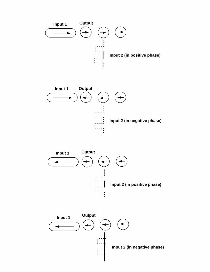
Input 1
Input 2 (in positive phase)
Output
Input 2 (in negative phase)
Output
Input 2 (in positive phase)
Output
Input 2 (in negative phase)
Output
Input 1
Input 1
Input 1

logic 1 logic 0
?
?
Input 1 Input 2Output
dipole-dipoleinteraction
dipole-dipoleinteraction

(a)
(b)
(c)
(d)
(e)

(a)
(b)
(c)
(d)
(e)
global clock
Inputwriter

(a)
(b)
θ

A nanowire with a cusp reverses the direction of domain wall motion and acts as a NOT gate
Magneticfield
Input (logic 1)
Output (logic 0)
A fork provides fan out
(a)
(b)

1 2 3 4 5
M
C
n-type semiconductorIinput
1 Iinput
2
Spinaccumulationregion
Vbat Vbat
d d
ACPSline
ACPSline
ACPSline
Ferromagnetic film (spin wave guide)
Silicon dioxide
Silicon