
multi-level gate circuits nand and nor gates
25
LECTURE 7 UNIT 7 MULTI-LEVEL GATE CIRCUITS NAND AND NOR GATES
-
Upload
khangminh22 -
Category
Documents
-
view
0 -
download
0
Transcript of multi-level gate circuits nand and nor gates

LECTURE 7
UNIT 7MULTI-LEVEL GATE CIRCUITS
NAND AND NOR GATES
OBJECTIVES
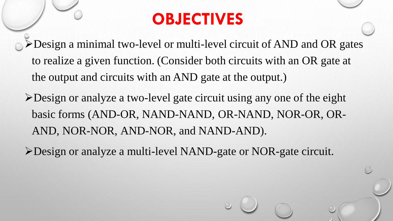
Design a minimal two-level or multi-level circuit of AND and OR gates
to realize a given function. (Consider both circuits with an OR gate at
the output and circuits with an AND gate at the output.)
Design or analyze a two-level gate circuit using any one of the eight
basic forms (AND-OR, NAND-NAND, OR-NAND, NOR-OR, OR-
AND, NOR-NOR, AND-NOR, and NAND-AND).
Design or analyze a multi-level NAND-gate or NOR-gate circuit.
OBJECTIVES
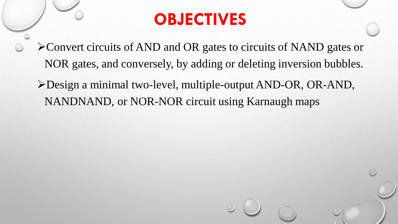
Convert circuits of AND and OR gates to circuits of NAND gates or
NOR gates, and conversely, by adding or deleting inversion bubbles.
Design a minimal two-level, multiple-output AND-OR, OR-AND,
NANDNAND, or NOR-NOR circuit using Karnaugh maps
7.1 MULTI-LEVEL GATE CIRCUITS
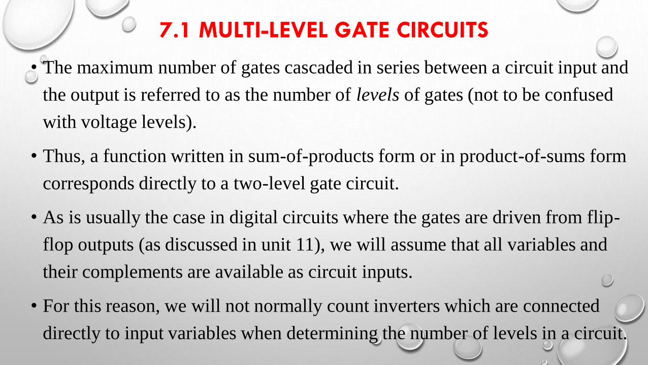
• The maximum number of gates cascaded in series between a circuit input and
the output is referred to as the number of levels of gates (not to be confused
with voltage levels).
• Thus, a function written in sum-of-products form or in product-of-sums form
corresponds directly to a two-level gate circuit.
• As is usually the case in digital circuits where the gates are driven from flip-
flop outputs (as discussed in unit 11), we will assume that all variables and
their complements are available as circuit inputs.
• For this reason, we will not normally count inverters which are connected
directly to input variables when determining the number of levels in a circuit.
7.1 MULTI-LEVEL GATE CIRCUITS
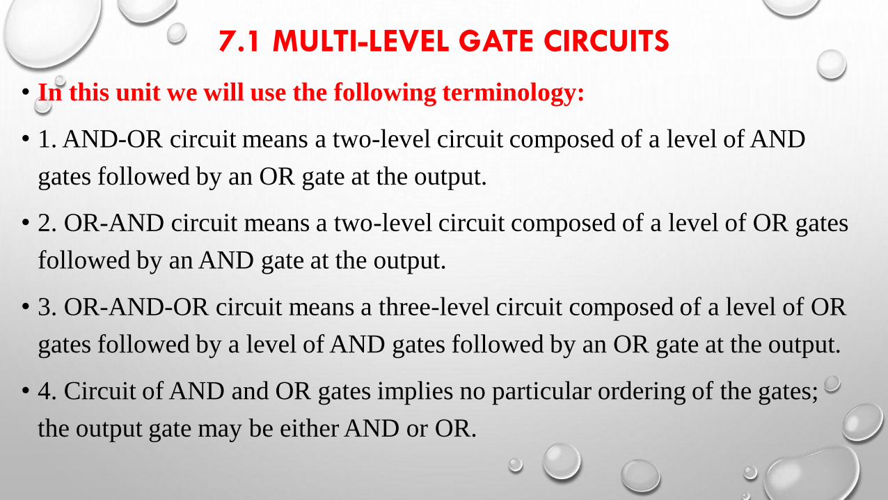
• In this unit we will use the following terminology:
• 1. AND-OR circuit means a two-level circuit composed of a level of AND
gates followed by an OR gate at the output.
• 2. OR-AND circuit means a two-level circuit composed of a level of OR gates
followed by an AND gate at the output.
• 3. OR-AND-OR circuit means a three-level circuit composed of a level of OR
gates followed by a level of AND gates followed by an OR gate at the output.
• 4. Circuit of AND and OR gates implies no particular ordering of the gates;
the output gate may be either AND or OR.
7.1 MULTI-LEVEL GATE CIRCUITS
• The number of levels in an AND-OR circuit can usually be increased by
factoring the sum-of-products expression from which it was derived.
Similarly, the number of levels in an OR-AND circuit can usually be increased
by multiplying out some of the terms in the product-of-sums expression from
which it was derived.
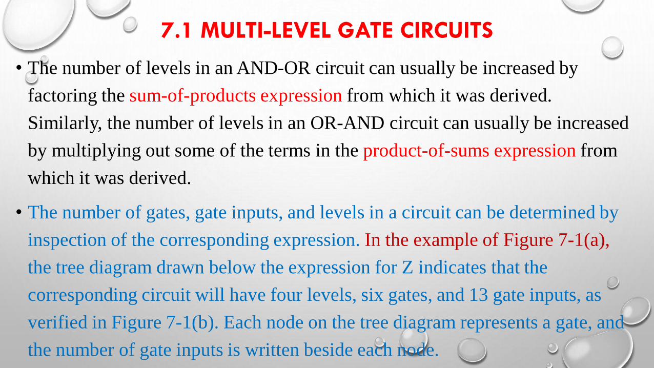
• The number of gates, gate inputs, and levels in a circuit can be determined by
inspection of the corresponding expression. In the example of Figure 7-1(a),
the tree diagram drawn below the expression for Z indicates that the
corresponding circuit will have four levels, six gates, and 13 gate inputs, as
verified in Figure 7-1(b). Each node on the tree diagram represents a gate, and
the number of gate inputs is written beside each node.
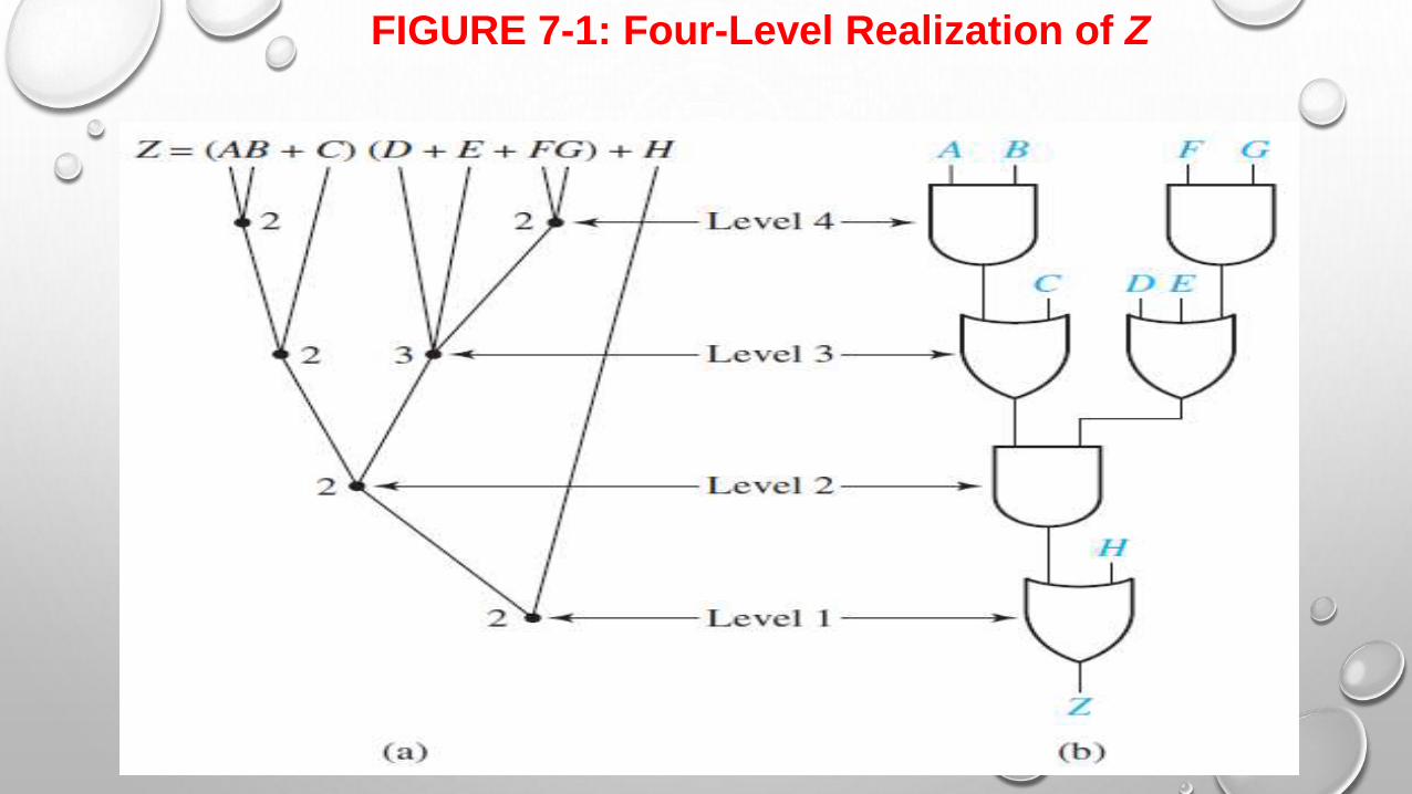
FIGURE 7-1: Four-Level Realization of Z

EXAMPLE OF MULTI-LEVEL DESIGN USING AND AND OR GATES
• Find a circuit of AND and OR gates to realize
Consider solutions with two levels of gates and three levels of gates. Try to
minimize the number of gates and the total number of gate inputs. Assume that
all variables and their complements are available as inputs.
Solution: First, simplify f by using a Karnaugh map (Figure 7-3):
This leads directly to a two-level AND-OR gate circuit (Figure 7-4):
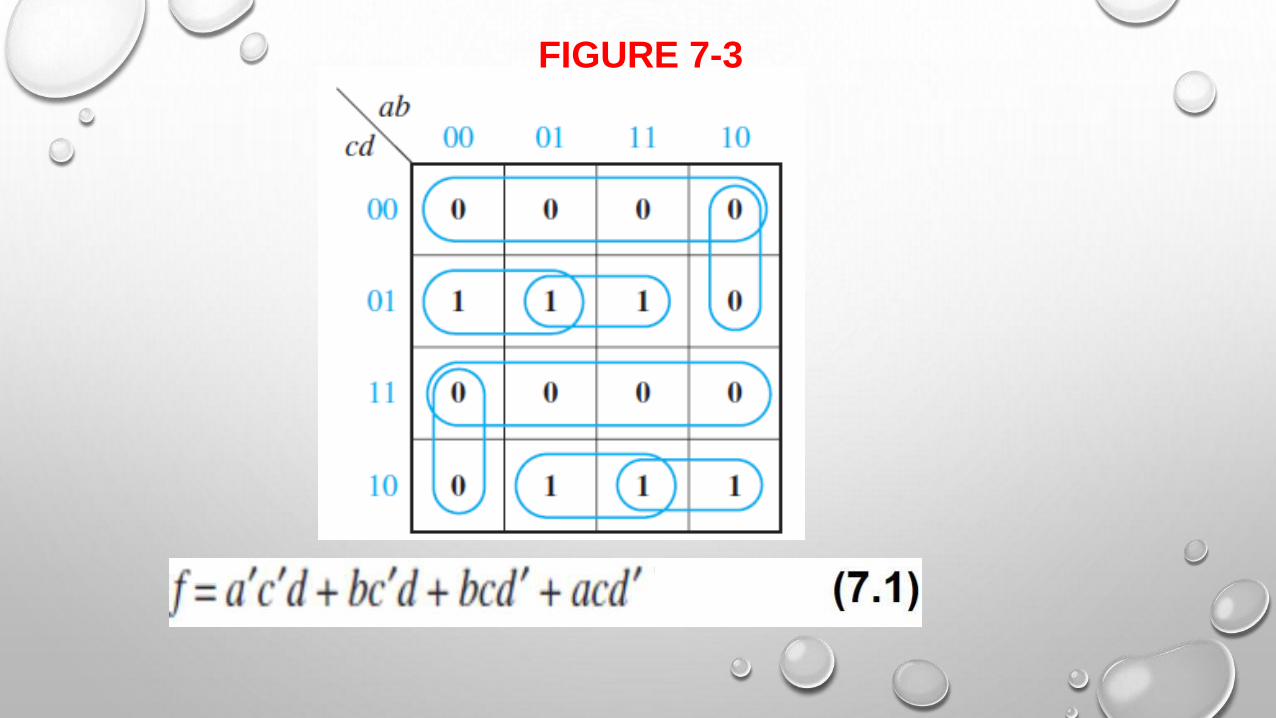
FIGURE 7-3
FIGURE 7-4
EXAMPLE OF MULTI-LEVEL DESIGN USING AND AND OR GATES
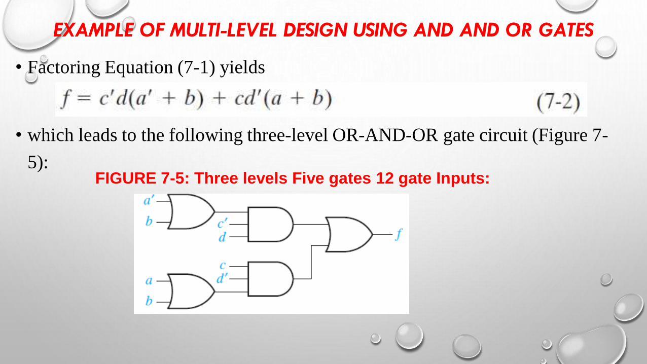
• Factoring Equation (7-1) yields
• which leads to the following three-level OR-AND-OR gate circuit (Figure 7-
5):FIGURE 7-5: Three levels Five gates 12 gate Inputs:
EXAMPLE OF MULTI-LEVEL DESIGN USING AND AND OR GATES
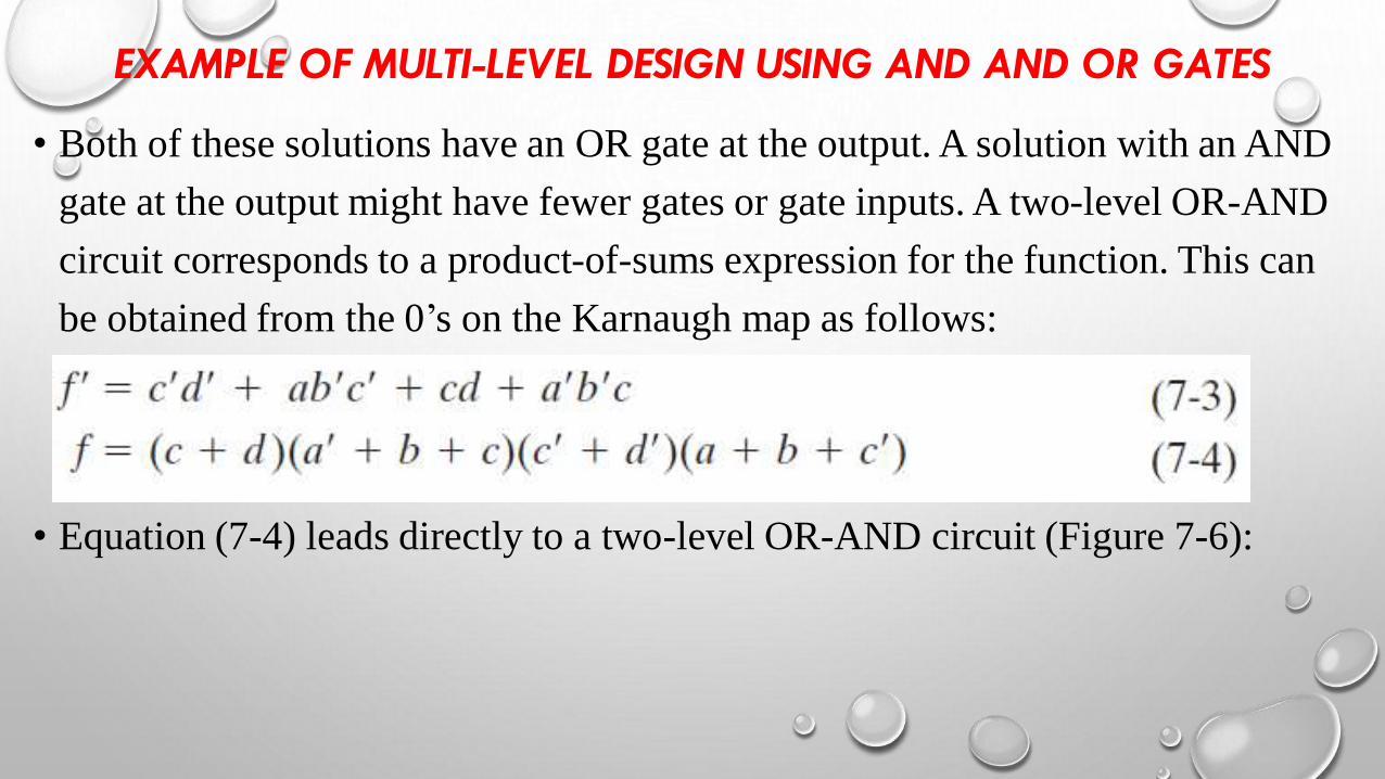
• Both of these solutions have an OR gate at the output. A solution with an AND
gate at the output might have fewer gates or gate inputs. A two-level OR-AND
circuit corresponds to a product-of-sums expression for the function. This can
be obtained from the 0’s on the Karnaugh map as follows:
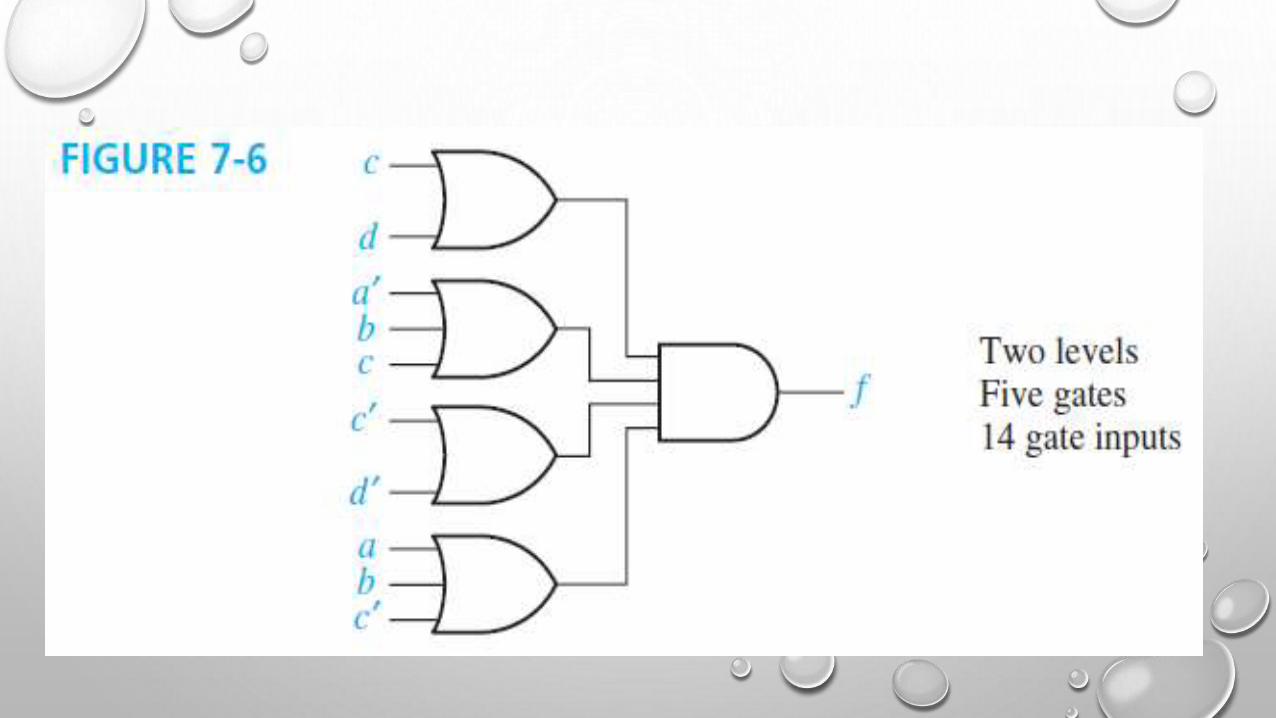
• Equation (7-4) leads directly to a two-level OR-AND circuit (Figure 7-6):

7.2 NAND AND NOR GATES
• In this section we will define NAND and NOR gates.
• Logic designers frequently use NAND and NOR gates because they are
generally faster and use fewer components than AND or OR gates.
• As will be shown later, any logic function can be implemented using only
NAND gates or only NOR gates. Figure 7-8(a) shows a three-input NAND
gate.
• The small circle (or “bubble”) at the gate output indicates inversion, so the
NAND gate is equivalent to an AND gate followed by an inverter, as shown
in figure 7-8(b).
7.2 NAND AND NOR GATES
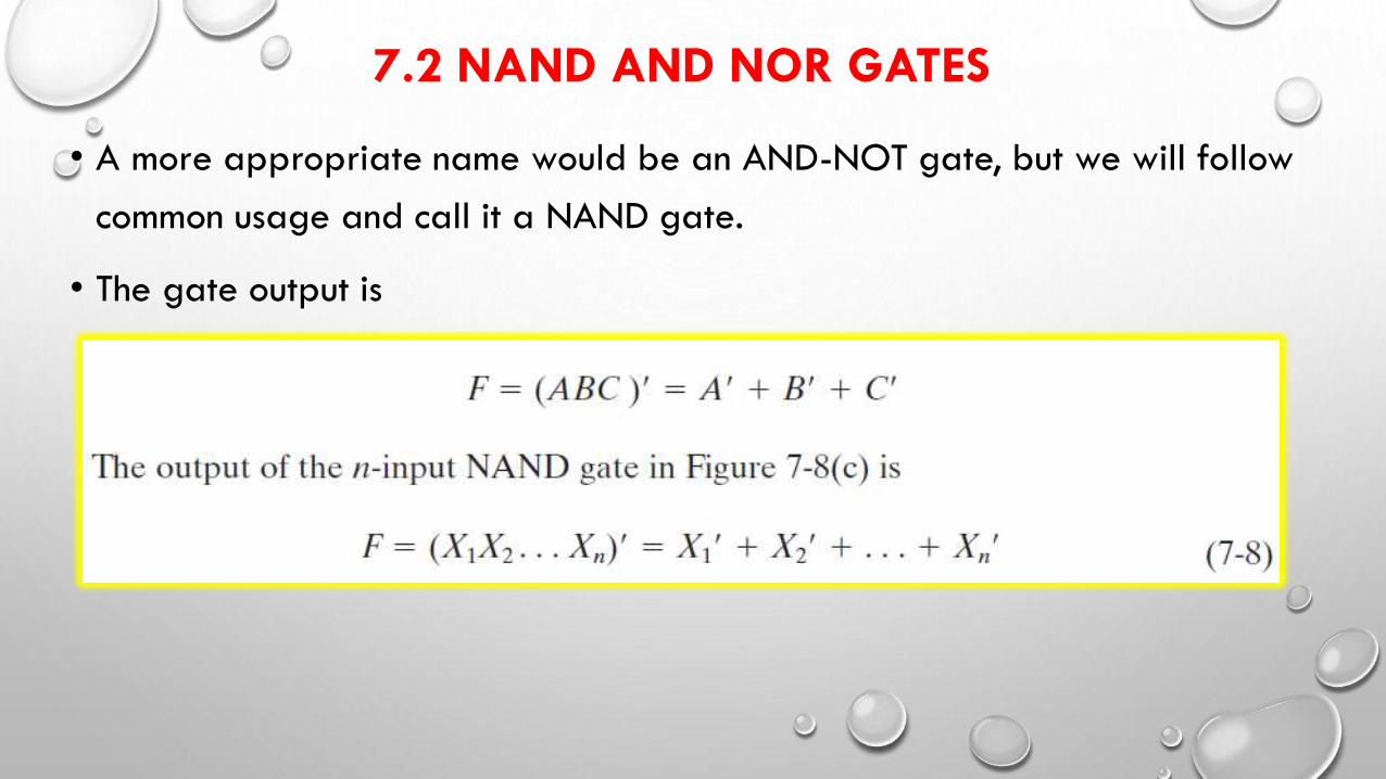
• A more appropriate name would be an AND-NOT gate, but we will follow
common usage and call it a NAND gate.
• The gate output is
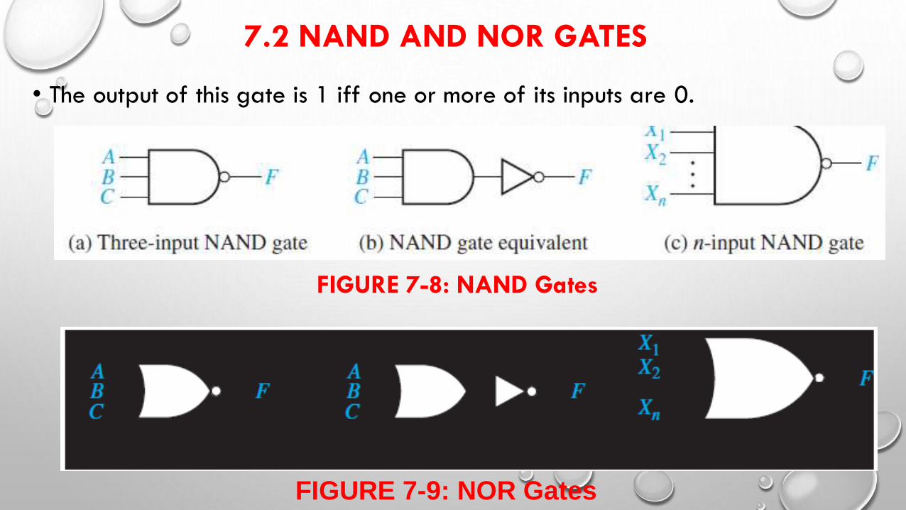
7.2 NAND AND NOR GATES
• The output of this gate is 1 iff one or more of its inputs are 0.
FIGURE 7-8: NAND Gates
FIGURE 7-9: NOR Gates
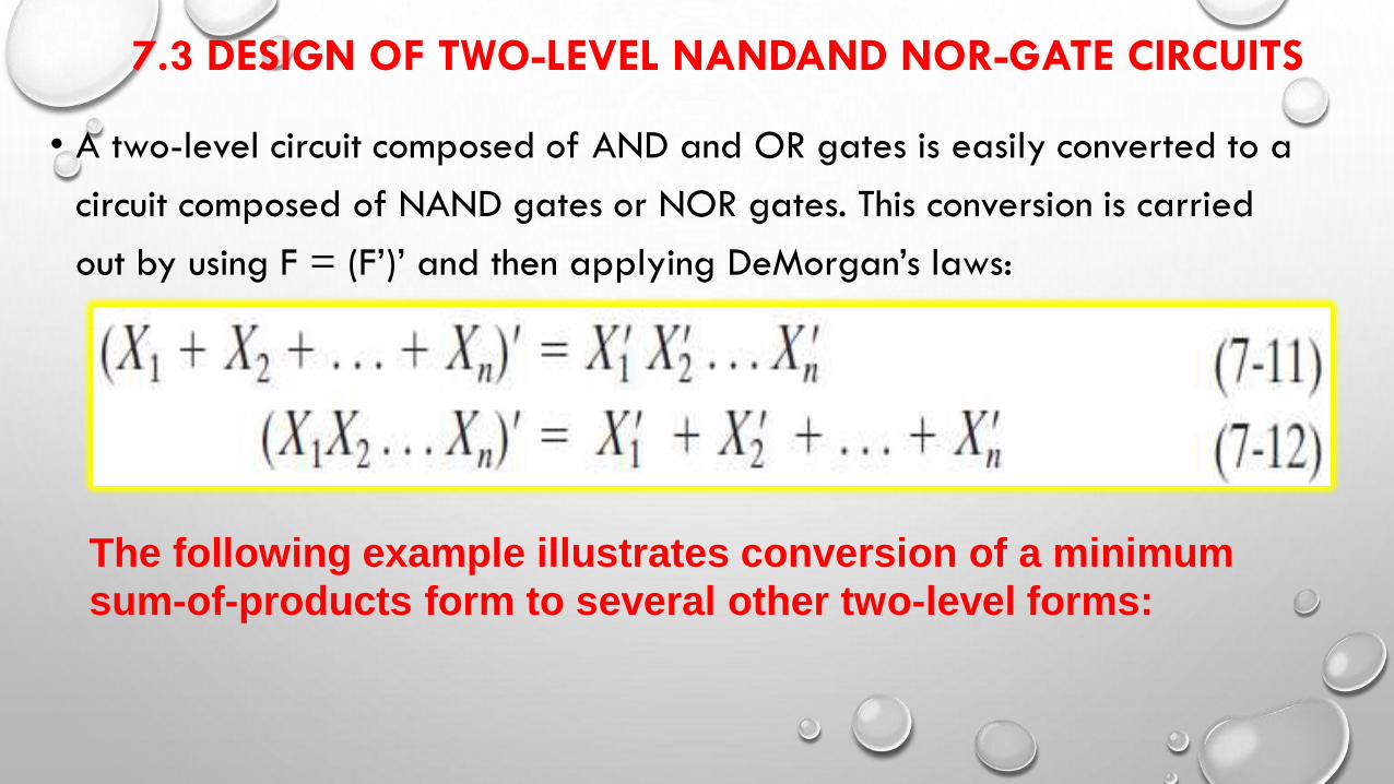
7.3 DESIGN OF TWO-LEVEL NANDAND NOR-GATE CIRCUITS
• A two-level circuit composed of AND and OR gates is easily converted to a
circuit composed of NAND gates or NOR gates. This conversion is carried
out by using F = (F’)’ and then applying DeMorgan’s laws:
The following example illustrates conversion of a minimum
sum-of-products form to several other two-level forms:
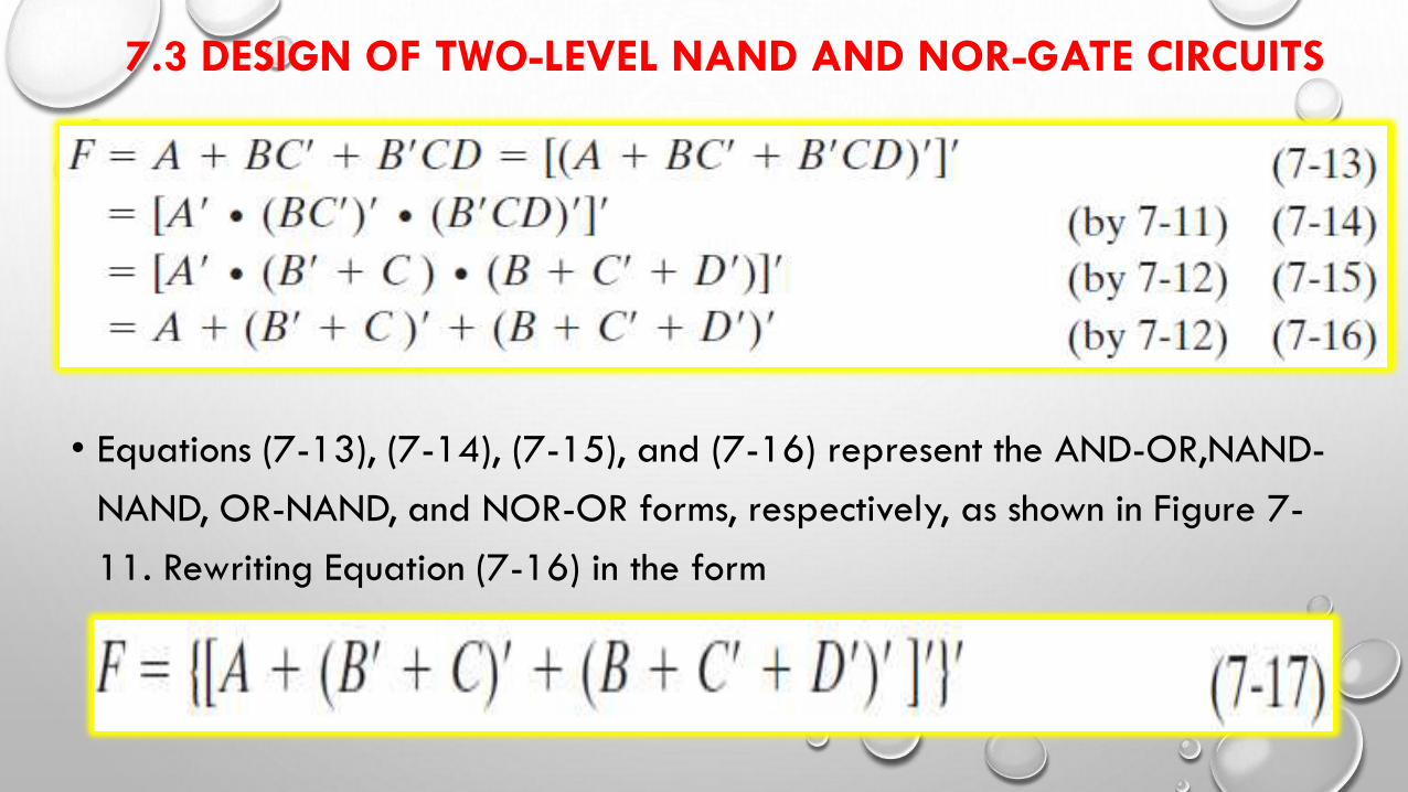
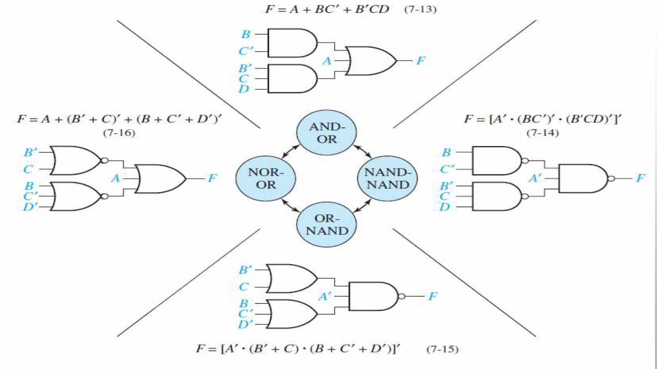
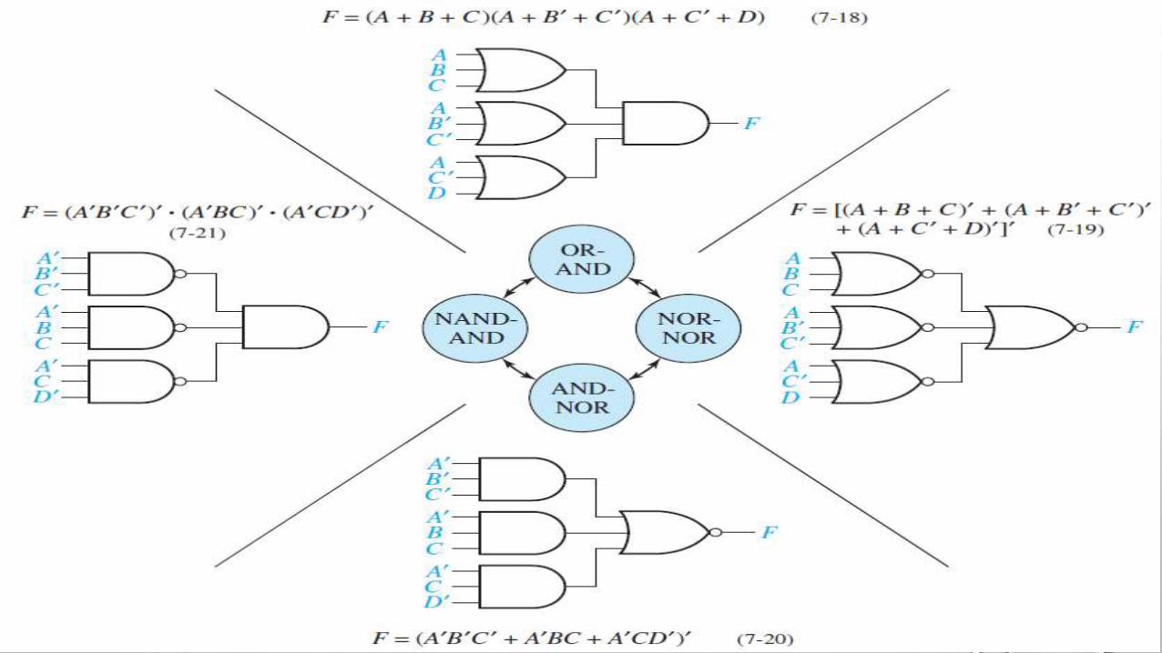
7.3 DESIGN OF TWO-LEVEL NAND AND NOR-GATE CIRCUITS
• Equations (7-13), (7-14), (7-15), and (7-16) represent the AND-OR,NAND-
NAND, OR-NAND, and NOR-OR forms, respectively, as shown in Figure 7-
11. Rewriting Equation (7-16) in the form
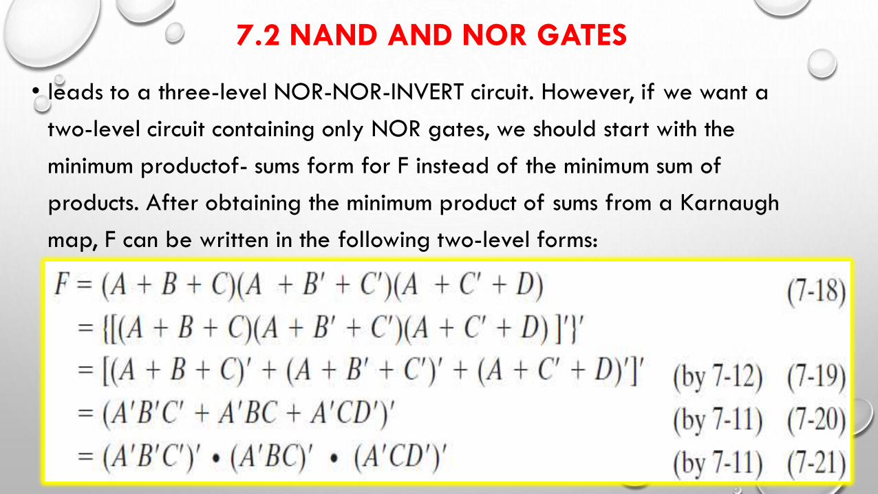
7.2 NAND AND NOR GATES
• leads to a three-level NOR-NOR-INVERT circuit. However, if we want a
two-level circuit containing only NOR gates, we should start with the
minimum productof- sums form for F instead of the minimum sum of
products. After obtaining the minimum product of sums from a Karnaugh
map, F can be written in the following two-level forms:
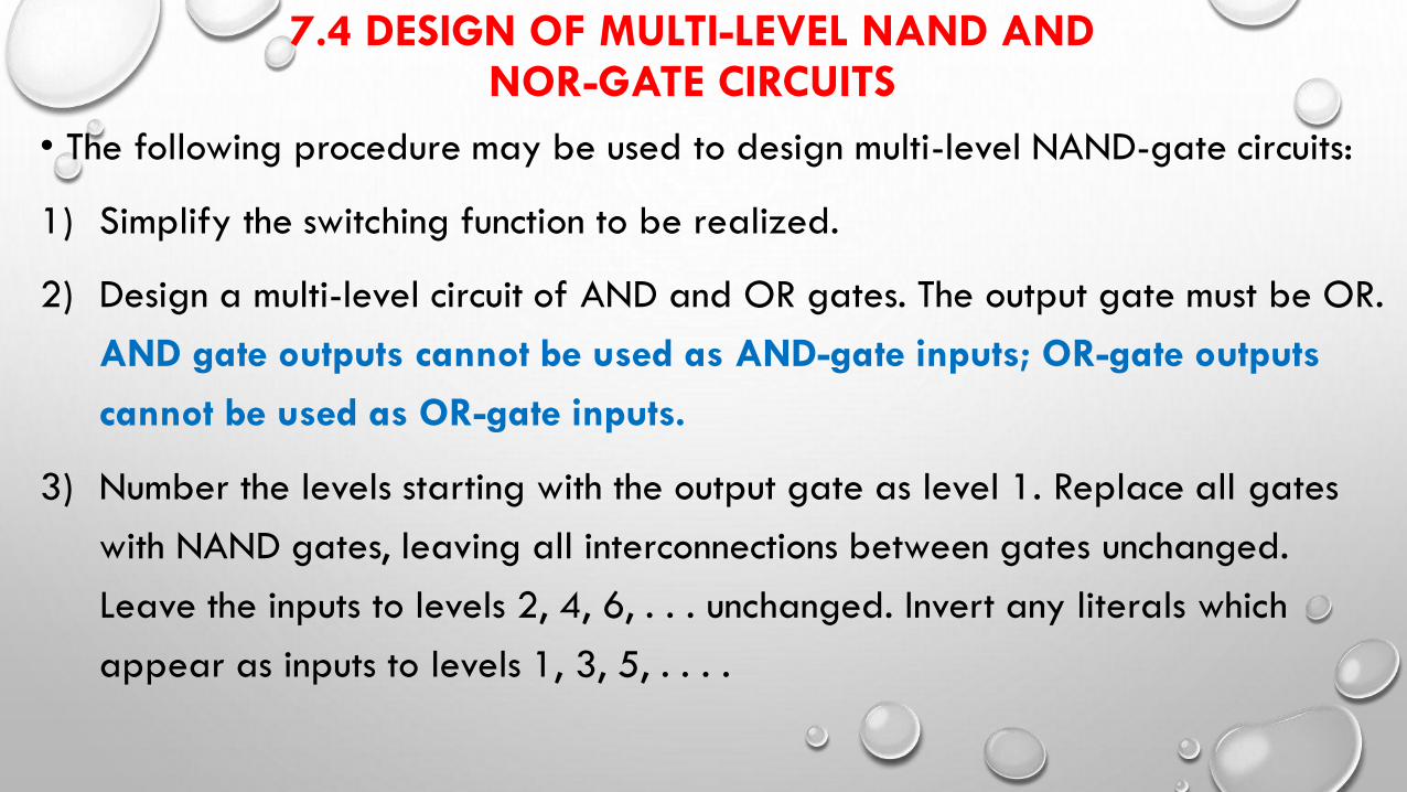
7.4 DESIGN OF MULTI-LEVEL NAND ANDNOR-GATE CIRCUITS
• The following procedure may be used to design multi-level NAND-gate circuits:
1) Simplify the switching function to be realized.
2) Design a multi-level circuit of AND and OR gates. The output gate must be OR.
AND gate outputs cannot be used as AND-gate inputs; OR-gate outputs
cannot be used as OR-gate inputs.
3) Number the levels starting with the output gate as level 1. Replace all gates
with NAND gates, leaving all interconnections between gates unchanged.
Leave the inputs to levels 2, 4, 6, . . . unchanged. Invert any literals which
appear as inputs to levels 1, 3, 5, . . . .
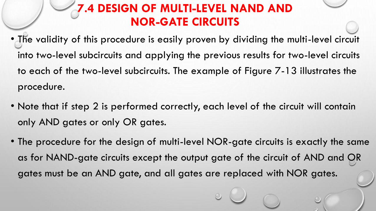
7.4 DESIGN OF MULTI-LEVEL NAND ANDNOR-GATE CIRCUITS
• The validity of this procedure is easily proven by dividing the multi-level circuit
into two-level subcircuits and applying the previous results for two-level circuits
to each of the two-level subcircuits. The example of Figure 7-13 illustrates the
procedure.
• Note that if step 2 is performed correctly, each level of the circuit will contain
only AND gates or only OR gates.
• The procedure for the design of multi-level NOR-gate circuits is exactly the same
as for NAND-gate circuits except the output gate of the circuit of AND and OR
gates must be an AND gate, and all gates are replaced with NOR gates.

7.4 DESIGN OF MULTI-LEVEL NANDANDNOR-GATE CIRCUITS
• EXAMPLE
Figure 7-13 shows how the AND-OR circuit for F1 is converted to the
corresponding NAND circuit.
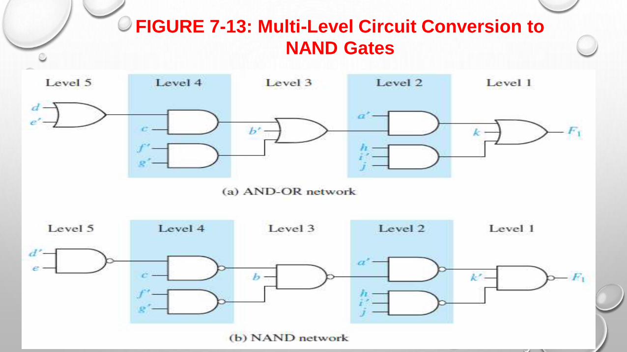
FIGURE 7-13: Multi-Level Circuit Conversion to
NAND Gates