Electrical and optical properties of materials Part 1. Conductivity
29
Electrical and optical properties of materials JJL Morton Electrical and optical properties of materials John JL Morton Part 1. Conductivity: from insulators to su- perconductors We will begin this lecture course with an overview of the forms of electrical conduction covered in earlier lectures, namely by free electrons, and see how metals, semiconductors and insulators differ in this respect. We will then move onto other forms of electrical conduction, such as by diffusion of ions in ionic solids, and by Cooper pairs in superconductors, giving essentially zero resistivity. 1.1 Electrical conductivity by free electrons Electrons obey the Pauli exclusion principle and cannot occupy the same state. They therefore must occupy a range of energy levels up to a maximum — at 0 K this maximum is well defined and termed the Fermi energy, E F . As the temperature is increased above absolute zero, the distribution of energies smears around the Fermi energy, such that the only vacant energy states can be found around E F . The behaviour of the electrons around E F is therefore critical for defining the electrical conductivity (and other properties) of the material. The outermost electrons in solids can often be modelled as free (or ‘nearly free’) carriers, in a weak periodic potential from the positive ions in the lattice. The effect of the lattice is to introduce discrete energy bands of allowed electronic states. This further imposes restrictions on the number of free electrons available for electrical conduction. 1.1.1 Metals In metals, E F lies within a band of allowed states, so there is no shortage of available carriers for conduction. Conductivity is determined by the scat- tering properties of the material (mean free path between scattering events) and by the electron velocity between scattering events (the Fermi velocity ). Electrical conductivity is defined as: σ = j/E, (1.1) where j is the current density (in units of A/m -2 ) and E is the applied electric field (in units of V/m). The equation of motion for the electron 1
-
Upload
khangminh22 -
Category
Documents
-
view
1 -
download
0
Transcript of Electrical and optical properties of materials Part 1. Conductivity

Electrical and optical properties of materials JJL Morton
Electrical and optical properties of materialsJohn JL Morton
Part 1. Conductivity: from insulators to su-perconductors
We will begin this lecture course with an overview of the forms of electricalconduction covered in earlier lectures, namely by free electrons, and see howmetals, semiconductors and insulators differ in this respect. We will thenmove onto other forms of electrical conduction, such as by diffusion of ions inionic solids, and by Cooper pairs in superconductors, giving essentially zeroresistivity.
1.1 Electrical conductivity by free electrons
Electrons obey the Pauli exclusion principle and cannot occupy the samestate. They therefore must occupy a range of energy levels up to a maximum— at 0 K this maximum is well defined and termed the Fermi energy, EF . Asthe temperature is increased above absolute zero, the distribution of energiessmears around the Fermi energy, such that the only vacant energy states canbe found around EF . The behaviour of the electrons around EF is thereforecritical for defining the electrical conductivity (and other properties) of thematerial.
The outermost electrons in solids can often be modelled as free (or ‘nearlyfree’) carriers, in a weak periodic potential from the positive ions in thelattice. The effect of the lattice is to introduce discrete energy bands ofallowed electronic states. This further imposes restrictions on the number offree electrons available for electrical conduction.
1.1.1 Metals
In metals, EF lies within a band of allowed states, so there is no shortageof available carriers for conduction. Conductivity is determined by the scat-tering properties of the material (mean free path between scattering events)and by the electron velocity between scattering events (the Fermi velocity).Electrical conductivity is defined as:
σ = j/E, (1.1)
where j is the current density (in units of A/m−2) and E is the appliedelectric field (in units of V/m). The equation of motion for the electron
1

1. Conductivity: from insulators to superconductors
under an electric field E is:
−eE = medv
dt(1.2)
We integrate over a period between collisions, τ . On each scattering event, itis impossible to know what the change in electron velocity will be, but we cansay that it has some average non-zero value (remember velocity is a vectorquantity) otherwise there would be no net current flow. We call this averageresultant electron velocity the drift velocity, or vd. This is in contrast to theFermi velocity, vF , which is the velocity between scattering events. Thus,
−eEτ = mevd (1.3)
We can write the time between collisions, τ , in terms of the Fermi velocityand a mean scattering length (or mean free path), λs.
τ = λs/vF (1.4)
Thus:
j = −nevd =ne2EλsmevF
(1.5)
σ =ne2λsmevF
, (1.6)
where n is the density of free electrons. Typical values are σCu = 108 (Ωm)−1,vF = 106 ms−1, n = 1029 m−3. These values give a mean free path λ ≈ 3.5×10⁻⁸ m, or about 100 atoms. It is therefore not the periodic lattice which isscattering electrons, but deviations from the perfect lattice such as vibrations(which show a linear temperature dependence at elevated temperatures andgo away at low temperatures), and impurities/vacancies etc. in the lattice(which show no temperature dependence).
Figure 1.1: The resistivity of a typical metal as a function of temperature
2
Electrical and optical properties of materials JJL Morton
Figure 1.2: Summary of conductivity versus temperature for metals, semi-conductors and insulators. Note the log scale for conductivity.
3

1. Conductivity: from insulators to superconductors
1.1.2 Semiconductors and insulators
In semiconductors and insulators, the Fermi energy lies in the middle of aband gap — a region of forbidden energy states. At low temperatures thereis therefore a negligible number of electrons with sufficient energy to crossthe band gap and occupy the higher lying states. The electrical conductivityis therefore determined primarily by the free carrier concentration whichdepends exponentially on temperature and the band gap energy Eg.
σ ∝ n ∝ exp (−Eg/2kBT ) (1.7)
The distinction between semiconductors and insulators essentially lies inthe magnitude of the band gap, compared with room temperature (belowabout 3.5 eV, materials are generally termed semiconductors). Note thatdiamond, for example, has a band-gap of 5.5 eV and is an excellent insulatorat room temperature. However, at high temperatures it would make a prettygood semiconductor. Semiconductors would be far less interesting if thestory ended here. They can be doped with impurities which artificially addfree electrons to the material, dramatically altering the conductivity (theycan also remove electrons from a full band creating ‘holes’ with an effectivepositive charge which are also capable of electrical conduction). It is thisproperty of being able to engineer regions of semiconductor with differentconducting properties which has made the semiconductor-based electronicsindustry possible.
Figure 1.3: The number of free carriers in semiconductors and insulators isexponentially dependent on temperature and the band gap energy
4
Electrical and optical properties of materials JJL Morton
1.2 Electrical properties of alkali halides
In the above section we revised the basic properties of conduction by freeelectrons, and found that in the case of insulators, the free electron concen-tration was negligible at room temperature. In this case, other mechanismsmay take over, such as conduction by ion transport. In this section we willdeal with the electrical and diffusional properties of ionic crystals by look-ing at a particular example, the alkali halides. The structures of the alkalihalides are well known, the most common being NaCl, being describable astwo interpenetrating face-centred cubic arrangements of positive and nega-tive ions, the origins of the two substructures being separated by half thecuvic cell edge. We are not concerned with the structure in any detail, ex-cept to note that there are equal numbers of positive and negative ions andthat the coordination number, Z, is 6 (i.e. each ion has 6 nearest neighboursof the opposite sign).
1.2.1 Intrinsic vacancy density
Clearly, the ability of ions to diffuse through a solid will depend strongly onthe concentration of vacancies for it to hop through. We therefore begin byusing a thermodynamic argument to estimate the vacancy density.
Recap Free energy = Internal energy - Temperature × Entropy
The free energy of the perfect crystal is:
Gp = Up − TSp (1.8)
While the free energy of the actual crystal has additional contributions fromthe vacancies (let there be N ions and n vacancies of each sign, so 2N ionsand 2n vacancies in total):
Ga = Gp + nφ− 2kBT ln [(N + n)!/N !n!]− Tn∆Sfreq (1.9)
Here, φ is the total energy of formation for a vacancy pair, one on each sub-lattice, not necessarily adjacent but not too far apart for electrostatic reasons.There are two ways in which the entropy has changed with the introductionof vacancies. The first is the configurational entropy term S = kB lnW , thesecond is associated with a change in the oscillator frequency of the ion whenit has a vacancy as its nearest neighbour (we define ∆Sfreq as the change inentropy due to change in oscillator frequency, per ion pair). We have alsoneglected any volume change created by introducing vacancies, which wouldproduce an additional term pV to the free energy).
5
1. Conductivity: from insulators to superconductors
We differentiate and set to zero to find the equilibrium number of vacan-cies, making use of Stirling’s approximation (ln x! ≈ x lnx− x):
∂Ga
∂n= φ− 2kBT [ln(N + n)− lnn]− T∆Sfreq = 0 (1.10)
Making the assumption that N >> n, this simplifies to:
n = N exp
(∆Sfreq
2kB− φ
2kBT
)(1.11)
Calculating ∆Sfreq depends in detail on the model chosen to representvibrations in the solid, but all models produce the same overall behaviourwhich is typified by the Einstein model of 3N harmonic oscillators per ionfor each direction x, y, z.
The entropy of one oscillator with angular frequency ω is given by (seewebnotes for a derivation, or a statistical mechanics text book):
S = kB[1 + ln (kBT/~ω)] (1.12)
We have 2N ions, and thus 6N oscillators, so in the perfect crystal:
Sp = 6NkB + 6NkB ln (kBT/~ω)] (1.13)
In the actual crystal with 2n vacancies and coordination number Z, therewill be 2nZ ions abutting onto vacancies, and so 6nZ of these oscillators willhave some lower frequency ω′:
Sa = (6N − 6nZ)
(kB + kB ln
kBT
~ω
)+ 6nZ
(kB + kB ln
kBT
~ω′
)(1.14)
∆Sfreq =Sa− Sp
n= 6ZkB ln
ω
ω′(1.15)
Plugging this back into Eq. 1.11, we get:
n
N=( ωω′
)3Zexp
(−φ
2kBT
)= C exp
(−φ
2kBT
)(1.16)
Adding a vacancy adjacent to an ion reduces the interatomic forces it expe-riences, and hence the vibrational frequency drops. Hence ω′ < ω and weexpect C to be greater than 1. The prefactor C is not strongly temperaturedependent. Similar expressions for ∆freq can be obtained from other models,but all produce something of the same form as the above. Note also thesimilarity between the form of this expression, and that of the number offree carriers in intrinsic semiconductors (see Eq. 1.7).
6
Electrical and optical properties of materials JJL Morton
Simple vacancies of the kind described above are not completely free:positive and negative ion vacancies will be attracted to each other as this re-duces their electrostatic energy. They may therefore form an associated pair,or even larger aggregates. Such restrictions limit their ability to conduct.
Other defects may be more mobile. For example, consider an associatepair of a (negatively charged) positive ion vacancy and positive ion interstitial(or the inverse version) which is known as a Frenkel defect. As electricalneutrality is maintained locally, there can be unequal numbers of Frenkelpairs of opposite sign. Again the same form of vacancy density results, withan additional correction (N is replaced with
√NNi):
n = C√NNi exp
(−φ
2kBT
)(1.17)
Ni is the number of possible interstitial sites in the crystal (e.g. Ni = 2N forthe [4] coordinated sites in fcc).
As with semiconductors, it is possible to dope the crystal with defectsto artificially increase the number of defects and thus tailor the conduct-ing properties of the material. For example, if a small quantity of CaCl2is dissolved in NaCl, the resulting crystal has the NaCl structure with theCl− sublattice perfect and the Na+ sublattice occupied at random by (i) amajority of Na+ ions, (ii) a minority of Ca2+ ions and (iii) an equal minor-ity of vacancies. This results in a temperature independent contribution tothe number of positive ion vacancies, necessary to preserve the structure,with local electrical neutrality preserved by the Ca2+ ions and positive ionvacancies tending to occur close to each other.
1.2.2 Self-diffusion of ions
The ability of particles to diffuse in a medium is characterised by the Diffusioncoefficent D, defined as the flux of particles (amount of substance diffusingthrough some area per unit time) given some concentration gradient (dN/dx).
J = −DdNdx
(1.18)
Einstein showed in 1905 while describing Brownian motion that this wasrelated to the mobility of particles, µ, where mobility is defined as the ratioof the drift velocity to the applied force:
Einstein relation D = µkBT
7

1. Conductivity: from insulators to superconductors
Figure 1.4: Energy barrier for hopping ion
For electrical conductors where the carriers have charge q, the appliedforce is qE. Thus,
D =vdkBT
qE(1.19)
Remembering that j = ncqvd = σE (where nc is the concentration of chargecarriers), we obtain a relation between the electrical conductivity and thediffusion coefficient:
σ =
(nce
2
kBT
)D (1.20)
We model diffusion of ions in solids as oscillators with frequency ν whichare held in their equilibrium position by an energy barrier of height εi (seeFigure 1.4). The probability of jumping to an adjacent site is therefore:
p = ν exp
(−εikBT
)(1.21)
The probability of that site actually consisting of a vacancy is n/N , andso the above probability must be multiplied by this factor. Following theordinary laws of kinetic theory, the diffusion coefficient may be shown to be:
D =1
3a2n
Np, (1.22)
where a is the jump distance. In Eq. 1.16 we obtained an expression forn/N for an intrinsic (un-doped) crystal. We can add to that a term arisingfrom extrinsic doping of defects next into the crystal using methods outlinedabove. Thus:
D =1
3a2ν exp
(−εikBT
)[next
N+ C exp
(−φ
2kBT
)](1.23)
lnD = lnνa2
3− εikBT
+ ln
[next
N+ C exp
(−φ
2kBT
)](1.24)
8

Electrical and optical properties of materials JJL Morton
ln Dln σT
1/T
high T
low T
slope = – (2εi+φ)2kB
slope = – εi/kB
increasing purity
Figure 1.5: The logarithm of D and σT versus reciprocal temperature. Sucha plot is termed an Arrhenius plot.
At high temperatures the intrinsic carriers in semiconductors outnumberthose from the dopants. Similarly, at high temperatures we can make theapproximation that intrinsic vacancies are dominant. Thus, at high temper-atures:
lnD = −2εi + φ
2kBT+
(lnνa2
3+ lnC
)(1.25)
Conversely, at low temperatures the number of vacancies will be dominatedby the extrinsic contribution, and we have:
lnD = − εikBT
+
(lnνa2
3+ ln
next
N
)(1.26)
In the two above results, the final term in brackets in a constant with tem-perature. The dependence of lnD, and thus ln(σT ), with temperature istherefore 1/T, with two different slopes in the high- and low-temperatureregions. The behaviour is sketched in Figure 1.5. Performing experiments tomeasure this temperature dependence across a sufficiently wide range there-fore allows the determination of φ and εi. For example, values obtained usingNaCl for the Na+ ion are:εi ∼ 0.77 eV = 1.23× 10⁻¹⁹ J = 74 kJmol−1
φ ∼ 2.06 eV = 3.30× 10⁻¹⁹ J = 198 kJmol−1
9

1. Conductivity: from insulators to superconductors
Figure 1.6: Energy barrier for hopping ion under the application of a voltageV
1.2.3 Ionic conductivity
The application of an electric field E creates an asymmetry in the potentialbarrier on either side of the ion by ±1
2aEe, as illustrated in Figure 1.6, so
the probability of jumps with, or against, the field become different:
p+ =ν
3exp
[−(εi −
eaE
2
)/kBT
](1.27)
p− =ν
3exp
[−(εi +
eaE
2
)/kBT
](1.28)
The rate of charge hopping in any one direction will be (n/N)p±, so theresulting current along one conducting chain of ions is:
Ichannel = en
N(p+ − p−) (1.29)
Figure 1.7 shows that for this particular NaCl crystal structure, one chain ofions has effective cross-sectional area of a2/2, so the overall current densityis:
j =2
a2en
N(p+ − p−) (1.30)
j =2
a2en
N
ν
3exp
(−εikBT
)[exp
(eaE
2kBT
)− exp
(−eaE2kBT
)](1.31)
At realistic electric fields, aEe << 2kBT , and thus we can approximateexp(x) = 1 + x...., giving:
σ =2e2ν
3akBT
n
Nexp
(−εikBT
)(1.32)
10

Electrical and optical properties of materials JJL Morton
area = a2/2
vol. = a3/2
conc. = 2/a3
a½
½
½
½
NaClfcc
atom spacing = a = acell/2
area per atom = a2cell/4 = a2/2
Figure 1.7: Calculation of area and volume factors for the NaCl fcc structure
Recalling the relationship between σ and D following the Einstein relation(Eq. 1.20), we can express the above in terms of D (from Figure 1.7 we seethat nc, the concentration of carriers is equal to 2/a3):
D =a2
3
n
Nν exp
(−εikBT
)(1.33)
This is identical to the expression used in Eq. 1.22. We have assumed thesame species / same mechanism is responsible for diffusion and conduction.Deviations from the Einstein relation indicate the breakdown of this assump-tion.
1.2.4 Which ion conducts?
The theory above was derived for the case of vacancies of one type of sitebeing responsible for all conduction. Generalisation to mixed conductivity isonly an algebraic difficulty. However, it is possible to experimentally deter-mine the relative importance of the two processes of conduction by positive ornegative ions. Two weighed slabs of salt M+X− are pressed together betweentwo weighed electrodes of the metal M. Electric current is passed throughthe cell. In the two extreme cases (see Figure 1.8):
a. If only positive ions conduct (i.e. via positive ion vacancies) the cathode[4] will grow at the expense of the anode [3]. The slabs of salt willremain unchanged in size, acting purely as conduction paths.
b. If only negative ions conduct (again via a vacancy mechanism) the X−
ions are neutralised at the anode [3] and form new layers of salt M+X−
by dissolving the metal. The salt layers are added to block [1] while
11

1. Conductivity: from insulators to superconductors
M
M
M+X–
M+X–[1]
[4]
[3]
[2]
+
–
Figure 1.8: Schematic of experiment used to determine relative contributionsof positive and negative ions to electrical conductivity
+ve ion dominates -ve ion dominatesakali halides: other halides:
Li, Na, K, Rb, Cs Pb, BaF, Cl, Br, I
silver halides
Table 1.1: Dominant ions for electrical conductivity in various ionic solids
the anode [3] decreases in weight. At the cathode [4], an equivalentnumber of metal ions M+ are deposited as neutral atoms from the saltlayers close by. Thus, salt block [2] also decreases in weight (efflux ofX− and deposition of M+ and the cathode [4] grows.
Weighing the electrodes and salt blocks before and after a measured quan-tity of electric charge has passed through the cell (checking for consistencyvia Faraday’s Law and relative atomic masses) enables the proportions ofconductivity modes to be deduced in the mixed case. In the alkali halides,the ion current is carried mainly by the positive ions, as is the case with thesilver halides.
12
Electrical and optical properties of materials JJL Morton
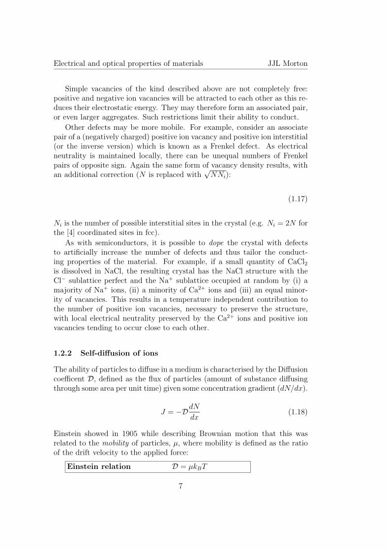
Figure 1.9: Ionic conductivity versus temperature in various superionic ma-terials
1.3 Superionic conductors
A subset of ionic conductors which have attracted particular interest are thesuperionic conductors (or fast-ion conductors). As the name implies, theyhave a very large conductivity compared with normal ionic conductors. Thetemperature dependence of some examples is shown in Figure 1.9. One of themost spectacular examples is silver iodide AgI: at the superionic transitionits conductivity increases by more than ×5000. There is a correspondingdecrease in the apparent activation energy for hopping εi — this is a keycharacteristic of the class of superionic conductors.
The transition is associated with a crystallographic phase change. The“super”-phase must have a transport mechanism which is especially efficient(e.g. via interstitial sites such as those illustrated in Figure 1.10). In theα-AgI structure there are 24 tetrahedral interstitial sites through which thesmaller positive Ag+ ion may move rapidly through the bcc lattice of I− ions.The structure is thus somewhat analogous to liquid crystals (covered later inthis course) — the lattice has partially melted (we can call it pseudo-moltenwith respect to Ag+, crystalline with respect to I−).
13

1. Conductivity: from insulators to superconductors
Figure 1.10: α-AgI structure
Figure 1.11: Sodium β-alumina electrolyte
Figure 1.12: Schematic of an Na-S cell (courtesy of Chloride Silent Power)
14

Electrical and optical properties of materials JJL Morton
1.3.1 Sodium-sulphur battery: Na β-Al2O3 electrolyte
Technologically one of the most important superionic systems may be sodiumβ-alumina (e.g. Na2O.11Al2O3) for use in the sodium-sulphur high temper-ature battery. Spinel blocks of Al3+ and O2− are separated by Al-O-Naconducting planes as shown in Figure 1.11. The Na+ ions in the conductingplanes are disordered and can move rapidly from site to site, giving the highconductivity. In the context of the Na-S battery, the fact that the Na istransported (as well as the electric charge) is not a problem — in fact, it iswhat’s needed for a battery to function.
A schematic of a Na-S battery is shown in Figure 1.12. Molten sodium inthe centre of the cell releases sodium ions into the electrolyte and electronsto the electrode. The sodium ions react with sulphur at the other electrodetaking up electrons. An EMF ξ is produced, defined as the energy gainedper unit charge:
ξ = −∆G
Fz(1.34)
∆G is the standard free energy (in units of J mol−1), z is the charge of theion (e.g. +1, +2 etc.), and F is the Faraday constant (defined as the electroncharge e times Avagadro’s number NA such that F = 96400 Cmol−1).
∆G = −RT ln
(a1a2
)(1.35)
ai is the activity (a measure of effective concentration) of a species at theelectrodes on either side of the electrolyte. Thus,
ξ =RT
Fzln
(a1a2
)(1.36)
For an Na-S cell, the EMF is 2.7 V.
1.4 Electron hopping (polaron) conduction
An alternative electron conduction mechanism may also play a role in certainimpure (or deliberately doped/alloyed) ionic solids if the metal cation canexist in different ionisation states (e.g. if it is a transition metal). As anillustration, if Li2O is added to NiO and the mixture fired under oxidisingconditions then the resulting crystal structure is found to contain Li+, Ni2+
and Ni3+ on the “Ni” sites of the NiO structure as indicated in Figure 1.13.An electron hopping from a Ni2+ ion to an adjacent Ni3+ ion transfers neg-ative charge in the direction of the hop and swaps the occupancy of the site
15

1. Conductivity: from insulators to superconductors
Figure 1.13: A polaron consists of an excess bound charge and associatedpolarisation of nearby ions
Poly(p-phenylene vinylene ) ‘PPV’ 2.4 eV ∼520 nmPolyacetylene 1.5-1.7 eV ∼780 nmPolyisothianaphtene 1.0-1.2 eV ∼1120 nm
Table 1.2: Some example band gaps for conducting polymers
in a way analogous to that of an ion hopping into a vacancy. Likewise, therewill be an activation energy associated with the transfer and so on. Again,there will be a logarithmic dependence of the diffusion coefficient with 1/T ,as shown in Figure 1.5.
The term polaron is sometimes used because the Ni3+ ion, being positivewith respect to the expected Ni2+ ion, polarises the surrounding oxygen ions.It is this composite entity which should be considered, not just electrontransfer between bare ions.
1.5 Conducting polymers
Typical organic polymers where the carbon atoms exhibit sp3 hybridizationare good insulators (e.g. PVC). However, in certain classes of polymer wherethere are alternating single-double bonds along a carbon backbone exhibit sp2
+ pz hybridization and there is the possibility of delocalised π-bond formationalong the chain involving the pz orbitals. The simplest example of such aconjugated polymer is polyacetylene (see Figure 1.14). Their behaviour ismuch like semiconductors, where excitation across a band gap is required topromote electrons to a delocalised energy where they are capable of electricalconduction. Some typical band gaps are given in Table 1.2 below.
Conducting polymers can be doped, just like traditional semiconductors.
16

Electrical and optical properties of materials JJL Morton
Figure 1.14: Structure of the most basic conjugated polymer: polyacetylene
Figure 1.15: Conductivity of polyacetylene doped with AsF5
17

1. Conductivity: from insulators to superconductors
This can be performed by adding electron-withdrawing or -donating side-chains to the polymer, or through electrochemical doping, or through a redoxagent. Figure 1.15 shows how the conductivity of polyacetylene varies withAsF5 doping concentration.
Polymer-based LED technology is an exciting way in which these mate-rials are being exploited to yield flexible displays with vibrant colours. PPVor poly (p-phenylenevinylene) is widely used in this context. Electrons areinjected from a negatively biased metal electrode (e.g. Ca or Al) and holesinjected from a semi-transparent electrode (e.g. indium tin oxide, ITO).The electrons and holes recombine within the polymer radiatively, emittinga photon at a wavelength given by the bandgap of the polymer. There areseveral processing advantages to polymer LEDs, and cost is widely toutedas an advantage though it is difficult to challenge the remarkably efficientsemiconductor industry in this regard. One major challenge which polymerLEDs have faced is the often short lifetimes of the devices, though there hasbeen much progress in this area in recent years and several polymer basedproducts (including large flat screen TVs) are now on the market.
18

Electrical and optical properties of materials JJL Morton
1.6 Superconductivity
The successful liquification of helium at the beginning of the 20th centuryopened the doors to a new temperature regime in which to explore the prop-erties of materials. There was considerable disagreement, for example, re-garding what would happen to the resistance of metals as the temperatureapproached absolute 0. Metals such as Cu, which are good conductors atroom temperature, where first measured. These showed a behaviour consis-tent with Figure 1.1 — scattering by impurities and defects dominated thelow temperature resistance of the material. Then in 1911, Kamerlingh Onnesbegan studying mercury as it could be more readily purified. His remarkablediscovery was that rather than a gradual change with temperature, there wasa sudden transition in the material to a state which appeared to have zeroresistance.
Figure 1.16: Heike Kamerlingh Onnes (left) in Leiden was the first to liquifyhelium in 1908, which then led to the discovery of superconductivity threeyears later. Also in the photo is Johannes Diderik van der Waals (right). Onthe right is the plot of the measured resistance of a mercurcy sample as afunction of temperature, as measured by Kamerlingh Onnes
1.6.1 What is the resistivity of a superconductor?
Experiments have been conducted since the 1950s which measure the decaytime for a current which has been established in a superconducting ring.For example, in 1961 a decay time of > 105 years was established (within
19

1. Conductivity: from insulators to superconductors
experimental error), providing an upper limit of 4 × 10⁻²⁵ Ωm for the su-peconducting resistivity. Subsequent experiments have measured limits downto ∼ 10−29 Ωm. These numbers can be contrasted with a good conductorsuch as copper, which does not superconduct: ρ(4.2 K)=∼ 7× 10⁻¹³ Ωm.
1.6.2 Superconducting elements
The table below shows the distribution of superconductivity amongst someof the elements. In addition, there are many hundreds of alloy systems whichare superconducting, and indeed it is these that are generally of most interestfor practical applications.
Table 1.3: Some of the superconducting elements and their superconductingtransition temperature, Tc in Kelvin in zero applied magnetic field for “pure”material. Boxes edged in single lines are Type I, double lines are Type II.
1.6.3 Magnetic field effects on superconductors
The excitement experienced by early researchers having discovered resistance-less conductivity is palpable. However, it soon became clear that some of theapplications one would envisage for this type of material were limited —passing a modest current or applying a modest magnetic field was enoughto turn the material back into the normal state. Therefore, in addition to acritical transition temperature Tc, superconductors can be characterised bycritical magnetic field and critical current values.
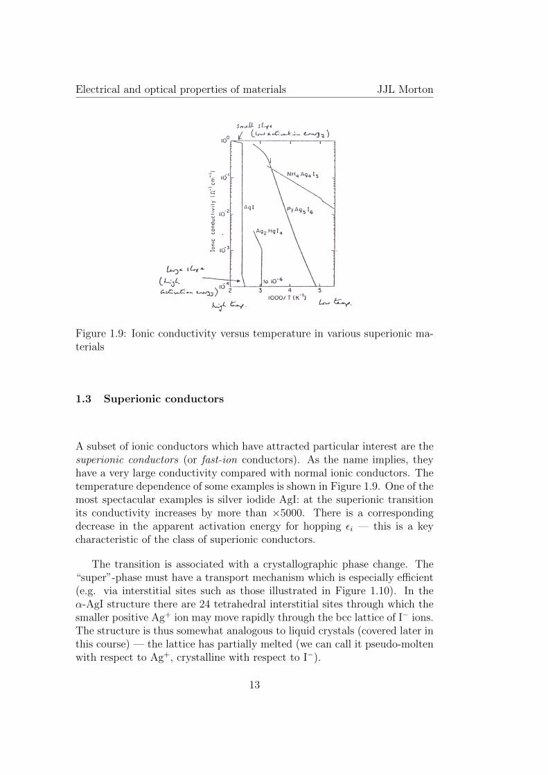
Twenty years later, Meissner discovered another fundamental property ofsuperconductors which differentiated them from a simple ‘perfect’ conductor.Material in a superconducting state completely expels an applied magneticfield — in other words it behaves as a perfect diamagnet. This is known as
20
Electrical and optical properties of materials JJL Morton
the Meissner effect, and illustrated in Figure 1.17. A perfect conductor willhave no internal electric field — Ohm’s law tells us E = ρj, so ρ→ 0 impliesE → 0. One of Maxwell’s equations (discussed in detail later in this course)relates the time variation of the magnetic field to the spatial variation of theelectric field:
Maxwell 3∂Ex∂z = −∂By
∂t
Given E = 0, this tells us that a perfect conductor must have ∂B/∂t = 0,but not necessarily B = 0. Hence, when a material which becomes perfectlyconducting below Tc is placed in a magnetic field and cooled through Tc ,the B field in the material stays constant, and is not expelled. On the other
Figure 1.17: Magnetic field lines around a perfect conductor, and a super-conductor, above and below the critical temperature
hand, when a superconductor is placed in a field and cooled through Tc, themagnetic field is expelled upon transition to the superconducting state. Inother words the material acquires a magnetisation, carried by surface currentloops, which is equal and opposite to the applied field. Such currents mustbe maintained ad infinitum, so for a material to be a perfect diamagnet inthis way it must also have zero resistance.
1.6.4 Magnetisation curve
For a specimen in the shape of a long thin rod with a magnetic field appliedparallel to its length, the geometry is termed “ideal”. The magnetisationcurve for such a specimen is shown in Figure 1.18, where H is plotted against−M (the magnetisation opposes the applied field). We’ll concentrate first onwhat are termed Type I superconductors shown on the left of the figure. Fol-lowing the Meissner effect, the magnetisation of the sample exactly opposesthe applied field, so −M = H up until a critical field, Hc. Above this field,
21

1. Conductivity: from insulators to superconductors
superconductivity is destroyed and the material returns to the normal state.Correspondingly, the resistivity (also plotted in Figure 1.18) becomes finiteat fields about Hc. In the ideal case, the magnetisation path is completelyreversible. The work done by the superconductor in expelling the applied
Magnetisation-M
-Hc
Magnetising field H
Hc
Resistivity
Magnetising field H
Hc
vortex state
Type I
Magnetisation-M
Magnetising field H
Hc (thermodyn)
Resistivity
Magnetising field H
Type II
Hc1 Hc2
Hc1 Hc2
superconducting state
Figure 1.18: Magnetisation and resistivity curves for Type I and Type IIsuperconductors, as a function of magnetising field H, below Tc
field is the area under the magnetisation curve of M vs B (where B = µH).Once this energy reaches a certain point, the superconducting state no longerbecomes favourable for the material, and it turns normal. If we call the freeenergy difference between the superconducting state and the normal state∆Gsuper (per unit volume), we can write:
∆Gsuper =1
2µH2
c (1.37)
Based on this magnetic field dependence, there are clearly implications forthe maximum current that can be passed through a superconductor whichwe will examine in a subsequent section.
1.6.5 Type I vs Type II superconductors
So far we have described the properties of so-called Type I superconductors,which we can think of as ideal, pure superconductors. A technologicallymore interesting class is the Type II superconductors, whose magnetic field
22

Electrical and optical properties of materials JJL Morton
dependence is shown on the right-hand part of Figure 1.18. We see twodistinct critical fields Hc1 and Hc2. For fields up to Hc1, the Meissner effectstill holds and the applied field is completely expelled, just as for a TypeI material. However, as the field is raised above Hc1, the magnetisationfalls off gradually until Hc2 where it drops to 0. The resistivity remainszero until Hc2, above which it becomes finite and the material returns tothe normal state. It is still possible to define the thermodynamic criticalfield Hc for Type II materials such that the area under the M -H curve is1/2 H2
c , which must lie between Hc1 and Hc2. Type II materials tend to bealloys, or transition metals with high values of resistivity in the normal state(see Figure 1.3). Furthermore, the magnetisation curve depicted for Type IImaterials is idealised, and one would expect some hysteresis in real materials.
The magnetisation behaviour of Type II superconductors is explained bythe penetration of magnetic flux into the material, creating small puddles ofnormal material within a superconducting bulk. The material is said to bein the mixed state or vortex state. Because the bulk of the materials remainsin the superconducting state, there remain conducting pathways of zero re-sistance, and hence the resistivity remains zero until the bulk turns normalat Hc2. The magnetic flux penetrates the material in discrete quanta Φ0,with a small screening current induced in the surrounding superconductingmaterial — hence, a vortex.
1.6.6 Flux quantisation
The derivation of the quantisation of flux into multiples of Φ0 lies beyondscope of this course. However, there is a nice argument based on the Aharonov-Bohm effect which illustrates the idea, as depicted in Figure 1.19. The
Figure 1.19: An illustration of the Aharonov-Bohm effect: in the absence ofscattering, a charge carrier will pick up different phases depending on whichpath it takes around some flux.
23

1. Conductivity: from insulators to superconductors
Aharonov-Bohm effect states that if we have two current paths, carried by acharge q, around either side of some flux Φ, and there is no scattering, thenthe phase difference ∆φ of the two paths is:
∆φ =qΦ
~(1.38)
If the two paths interfere in any way other than perfectly constructively,then the presence of the flux appears as a source of scattering, which thesuperconductor does not permit. We can therefore state that the supercon-ductor will only allow flux penetration in units where the two paths interfereconstructively, i.e. their relative phase must be a multiple of 2π.
∆φ =qΦ
~= 2Nπ and thus, Φ =
Nh
q= NΦ0 (1.39)
So the allowed flux is quantised in units of Φ0 = h/q. We can measure theflux quantum to be:
Φ0 =h
2e= 2× 10⁻¹⁵ Weber (1.40)
So, the charge carriers in superconductors appear to have a charge of twicethe electric charge... the entities responsible for electrical conduction in su-perconductors are electron pairs, known as Cooper pairs. If it seems coun-terintuitive that electrons should pair up in this way, don’t be discouraged— it was not until 46 years after the discovery of the phenomenon that asatisfactory theory for superconductivity was put forward! The paired state,where two electrons couple to the same lattice vibration, becomes energet-ically favourable below Tc. Electrons paired in this way cannot be readilyscattered, hence the resistance-less current flow.
1.6.7 The flux lattice
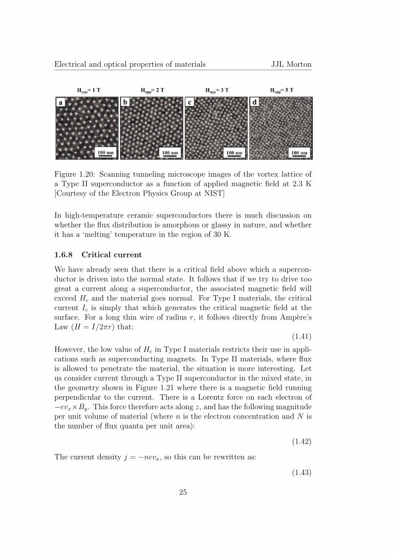
Using very small amounts of powder and replica techniques for the electronmicroscope, several research groups have imaged the flux lattice emergingfrom the surface of a Type II superconductor by decorating it with ferro-magnetic powder particles. More recently, the use of scanning tunnelingmicroscope (STM) at cryogenic temperatures has enabled the direct imagingof the regions of normal state of the material, and thus the flux lattice (seeFigure 1.20. The flux lattice is triangular, and has a lattice constant whichdecreases as the applied field increases. As with atomic lattices, movementsof flux-lattice dislocations, vacancies etc. are important to understand thebehaviour of the superconductor, especially when a field gradient is applied.
24
Electrical and optical properties of materials JJL Morton
Figure 1.20: Scanning tunneling microscope images of the vortex lattice ofa Type II superconductor as a function of applied magnetic field at 2.3 K[Courtesy of the Electron Physics Group at NIST]
In high-temperature ceramic superconductors there is much discussion onwhether the flux distribution is amorphous or glassy in nature, and whetherit has a ‘melting’ temperature in the region of 30 K.
1.6.8 Critical current
We have already seen that there is a critical field above which a supercon-ductor is driven into the normal state. It follows that if we try to drive toogreat a current along a superconductor, the associated magnetic field willexceed Hc and the material goes normal. For Type I materials, the criticalcurrent Ic is simply that which generates the critical magnetic field at thesurface. For a long thin wire of radius r, it follows directly from Ampere’sLaw (H = I/2πr) that:
Ic = 2πrHc (1.41)
However, the low value of Hc in Type I materials restricts their use in appli-cations such as superconducting magnets. In Type II materials, where fluxis allowed to penetrate the material, the situation is more interesting. Letus consider current through a Type II superconductor in the mixed state, inthe geometry shown in Figure 1.21 where there is a magnetic field runningperpendicular to the current. There is a Lorentz force on each electron of−evx×By. This force therefore acts along z, and has the following magnitudeper unit volume of material (where n is the electron concentration and N isthe number of flux quanta per unit area):
Fz = −nevxNΦ0 (1.42)
The current density j = −nevx, so this can be rewritten as:
Fz = jxNΦ0 (1.43)
25

1. Conductivity: from insulators to superconductors
e-
e-
j
Φ z
xyB
Figure 1.21: The effect of current on flux quanta
There must be an equal and opposite force on the flux lines. So if we apply afixed current j along the sample, each flux quantum experiences a force jΦ0
in a direction perpendicular to the current flow. If these flux lines are allowedto move under this force, we have a time-varying magnetic field, and by thesame Maxwell’s equation used above, an induced voltage (electric field perunit distance)
Maxwell 3∂Ex∂z = −∂By
∂t
Thus, we have an induced voltage which is proportional to the currentthrough the material — it looks like a resistor. Materials in the mixed statewith no flux pinning are therefore not capable of carrying much current.
1.6.9 Flux pinning
If the force derived above is insufficient to move the flux line through thematerial, it is possible for a large current to flow without resistance. Byequating this pinning force to that derived above, we obtain:
Fpinning = jcritΦ0 (1.44)
This argument is oversimplified, neglecting (i) the fact that the flux linesthrough the material are precisely due to the applied current in the firstplace and (ii) the effects of interactions between flux lines, amongst otherthings. However, it does illustrate the critical role which flux pinning playsin enabling superconductors to carry large currents and make them techno-logically useful. In looking for suitable materials from which to fabricate ahigh-field magnet, for example, we therefore require something with a com-bination of:
a. large flux pinning
b. high value of Hc2
26

Electrical and optical properties of materials JJL Morton
High temperature / high field alloys
Alloys tend to be Type II materials. Examples include:
Tc (K) Bc2 (T)Nb40-Ti60 9 10Nb3Sn 18.5 20Nb3(Ge0.8Al0.2) 10Chevrel phases 10 60
Table 1.4: Some superconducting alloys and compounds and their properties
There is still much basic research to be done into the underlying mechanismsof both these properties and so at present these qualities are mainly empiricalas we shall see when discussing actual materials in the following section. AType II superconductor is termed hard if the flux lines within it experiencea high pinning force.
1.6.10 Superconducting materials
Tables 1.4 and 1.5 survey some example values for critical temperature andfield in Type II superconductors. There is a very approximate correlationbetween Tc and Hc, but as seen from the Chevrel phase materials this doesn’talways hold. The whole panoply of complication of the metallurgical phasediagram spills over into superconductivity parameters such as Tc, as differentphases become stable in different composition ranges. Most of the work onthe alloys described in Table 1.4 was done before the 1980s, when attentionshifted towards the higher-Tc ceramic materials. Note that as usual, theapplication of these materials lags a decade or so behind their discovery.
In the 1980s, superconducting ceramic metals with ‘high’ critical temper-atures was discovered and they continue to attract considerable attention.Their general formula is (LxM1−x)mAnDp, where L is usually a rare earth,M an alkali earth, A is Cu (part 2+, part 3+) and D is oxygen. Someexamples are shown in Table 1.5.
1.6.11 Organic superconductors
There is also renewed interest in superconductors based on organic materials.Although the values of Tc and Jc are typically very low, they provide a usefultest bed to explore theories and subsequently improve the characteristics of
27

1. Conductivity: from insulators to superconductors
High temperature ceramic superconductors
Tc (K) structure(La2−xBax)CuO4−y 33 K2NiF4 structure (Nobel Prize 1987)YBa2Cu3O7 93 layered perovskiteBi2Sr2CaCu2Om 96 layer(Bi1−xPbx)2Sr2Ca2Cu3O11 110 layerTlBamCanCupOy up to 125 layer
Table 1.5: Some superconducting ceramic materials and their properties
other superconductors. An example is the layered charge transfer salt shownin Figure 1.22 where the current runs along the layers of Cu(CSN)2.
Figure 1.22: An example organic superconductor: k-BEDT-TTF2Cu(CSN)2
1.6.12 Superconducting materials for high field magnets
Following the arguments described earlier, the critical current must dependon temperature and externally applied magnetic field. For a fixed tempera-ture, applying an external magnetic field causes the critical current to fall.However, curves of Jc vs H for traditional ‘hard’ Type II materials typicallyexhibit a plateau, and sometimes even a peak effect. Figure 1.23 shows anexample for the 75Zr-25Hb alloy. In its purest (recrystallised) state it ex-hibits no plateau, just a reasonable monotically decreasing value of Jc withincreasing H. This is consistent with the flux in the material being due to thecombination of a term induced by current through the superconductor, plus
28

Electrical and optical properties of materials JJL Morton
an applied external field. The same material, only partially recrystallisedafter cold work has a much higher value of Jc at elevated fields. The highestvalues of all for this system are found after cold work and a particular heattreatment, the latter probably involving some precipitation due to the pres-ence of oxygen. If the scale of the precipitation, or of the dislocation tanglesin polygonised walls, is right, then large pinning (and high Jc) results.
The curve of Figure 1.23 is typical of superconducting wires for appli-cations in high-field magnets. Such curves are constantly being revised asmanufacturers vie with each other to produce better and better wires. Thefirst generation of wires were NbZr and NbTi (mostly the latter is used now,for example in the LHC in CERN). A second generation is Nb3Sn, which isused, for example, in fusion energy research.
Figure 1.23: Critical current density Jc versus applied field H
29