Manipulation of vortices by localized impurities in Bose-Einstein condensates
Upload
independentCategory
view
7download
0
arX
iv:c
ond-
mat
/030
8575
v1 2
7 A
ug 2
003
Electric Field Control of Shallow Donor Impurities in Silicon
A. S. Martins, R. B. Capaz, and Belita Koiller
Instituto de Fısica, Universidade Federal do Rio de Janeiro,
Cx.P. 68.528, 21945-970, RJ, Brazil
(Dated: February 2, 2008)
Abstract
We present a tight-binding study of donor impurities in Si, demonstrating the adequacy of this
approach for this problem by comparison with effective mass theory and experimental results. We
consider the response of the system to an applied electric field: donors near a barrier material and in
the presence of an uniform electric field may undergo two different ionization regimes according to
the distance of the impurity to the Si/barrier interface. We show that for impurities ∼ 5 nm below
the barrier, adiabatic ionization is possible within switching times of the order of one picosecond,
while for impurities ∼ 10 nm or more below the barrier, no adiabatic ionization may be carried out
by an external uniform electric field. Our results are discussed in connection with proposed Si:P
quantum computer architectures.
PACS numbers: 71.15.Ap, 71.55.-i, 71.55.Cn, 03.67.Lx
1

I. INTRODUCTION
Simple donors in Si have recently become the subject of renewed interest due to proposals
of quantum computer architectures in which P donors in Si play the role of qubits.1,2,3 Logic
operations in such architectures involve the response of the bound electron wavefunctions to
voltages applied to a combination of metal gates separated by a barrier material (e.g. SiO2)
from the Si host. The so-called A-gate, placed above each donor site, pulls the electron
wavefunction away from the donor, aiming at partial reduction1 or total cancelation3 of
the electron-nuclear contact coupling in architectures where the qubits are the 31P nuclear
spins. In a related proposal based on the donor electron spins as qubits,2 the gates drive
the electron wavefunction into regions of different g-factors, allowing the exchange coupling
between neighboring electrons to be tuned. Ideally, electric-field control over the donor
electron wavefunction requires all operations to be performed in the adiabatic regime4, which
sets a lower bound for the time scales involved in such processes.
Recent studies have demonstrated that the tight-binding (TB) approach, traditionally
adopted for deep levels,5 provides a valid description for intermediate6,7 and shallow levels8
in semiconductors. Impurity states are calculated from a sequence of supercell sizes and a
finite-size analysis which provides extrapolation to the bulk limit. Also, electric-field effects
may be easily incorporated within the TB scheme9, allowing estimates of switching times in
electric-field-tunable devices10. In this work we present a TB description for donors in Si,
aiming at a physical description of the relevant properties involved in the A-gate operations
mentioned above.
Donors in Si have been extensively and successfully investigated within the effective mass
theory (EMT),11 thus providing a preliminary test for the TB approach by comparison of
wavefunctions predicted by the two formalisms. This comparison is presented in the next
section. In Sec. III we explore a simplified model of the A-gate operations in the Kane
quantum computer proposal1 by considering the Si:P system under an uniform electric field
and near a barrier. In Sec. IV we discuss operation times and restrictions imposed by the
donor positioning with respect to the Si/barrier interface in connection with the adiabaticity
of the A-gate operations. Our summary and conclusions are presented in Sec. V.
2

II. TB DESCRIPTION FOR DONORS IN SILICON
A. Formalism
The TB Hamiltonian for the impurity problem is written as6
H =∑
ij
∑
µν
hµνij c
†iµcjν +
∑
i,ν
U(ri)c†iνciν (1)
where i and j label the atomic sites, µ and ν denote the atomic orbitals and ri is the distance
of the site i to the impurity site. The matrix elements hµνij define all the on-site energies and
first and second neighbors hoppings for the bulk material. The donor impurity potential
U(ri) is described by a screened Coulomb potential (ǫ = 12.1 for Si)
U (ri) = − e2
ǫri
. (2)
At the impurity site (ri = 0), the perturbation potential is assigned the value −U0, a param-
eter describing central cell effects characteristic of the substitutional species. In the present
calculations, U0 was kept as an adjustable parameter (previous estimates for this parameter6
are of the order of one to a few eV). We adopt here the sp3s∗ TB parametrization for Si pro-
posed by Klimeck et al,12 which includes first and second neighbors interactions. Inclusion of
hopping matrix elements up to second neighbors provides a good description of the effective
masses at the conduction band minima. This parametrization gives the k-space positions of
the six band minima at the six equivalent points along the ∆ lines, at ∆min = 0.75(2π/a),
where a = 5.431A is the conventional cubic lattice parameter for Si. We do not include
spin-orbit corrections in our calculations.
The eigenstates of H are determined for a system where a single impurity is placed in
a cubic supercell containing N = 8L3 atoms arranged in the diamond structure, where L
is the length of the supercell edge in units of a. The supercells are subject to periodic
boundary conditions, and full numerical diagonalization can be performed for L . 6. Much
larger supercells8 (up to 106 atoms) may be treated within a variational scheme13 where the
ground state wavefunction and binding energy EL for a donor level is obtained by minimizing
the expectation value of⟨Ψ
∣∣(H − εref)2∣∣ Ψ
⟩. For the donor ground state, εref is a reference
energy chosen well within the gap, but nearest to the conduction band minimum, and excited
states are obtained by tuning εref towards the conduction band edge. Finite size scaling
3

allows extrapolation to the bulk limit (L→ ∞) according to the ansatz6,7
EL = Eb + Ee−L/λ, (3)
where Eb is the binding energy for a single donor in the bulk.
The eigenfunctions of (1) written in the basis of atomic orbitals |φν(r − Ri)〉 are given
by |ΨTB(r)〉 =∑
iν aiν |φν(r −Ri)〉 where the expansion coefficients aiν give the probability
amplitude of finding the electron in the orbital ν localized at Ri. We do not include explicit
expressions for the atomic orbitals; the overall charge distribution is conveniently described
through the TB envelope function squared,14
|ΨEF (Ri)|2 =∑
ν
|aiν |2. (4)
B. Donor ground state
In the proposed TB model, the only free parameter is related to the on-site value for the
impurity potential, U0. In Fig. 1(a) we present the converged (L → ∞) binding energy of
the lowest donor state as a function of U0. We also characterize the donor ground state by
its orbital averaged spectral weight14 at ∆min
W (∆min) =2
N
6∑
µ=1
∑
ijν
eikµ·(Ri−Rj)aiνajν, (5)
where N is the number of atomic sites in the supercell, and the first summation is over the
six equivalent kµ at the conduction band minima. This quantity is plotted in Fig. 1(b) as a
function of U0.
We determine the value of U0 so that the binding energy of the donor results to be in good
agreement with the experimental value which, for P in Si, is Eb = 45.6 meV. As indicated
in Fig. 1, U0 = UP∼= 1.48 eV gives the correct binding energy for the P donors in Si. This
value for U0 is used in the calculations below.
C. Comparison with EMT
EMT exploits the duality between real and reciprocal space, where delocalization in real
space leads to localization in k-space, e.g. for shallow donors around the k-vector at the
4

minimum of the conduction band. Within EMT in its simplest formulation,11 the ground
state for donors in Si is six-fold degenerate, due to the six-fold degeneracy of the Si conduc-
tion band. Valley-orbit interactions15 lead to a non-degenerate ground state wavefunction
of A1 symmetry,16
ψ(r) =1√6
6∑
µ=1
Fµ(r)φµ(r) , (6)
where φµ(r) = uµ(r)eikµ·r are the pertinent Bloch wave functions, and the envelope functions
given by (e.g. for µ = z)17
Fz(r) =1√πa2b
e−[(x2+y2)/a2+z2/b2]1/2
. (7)
The effective Bohr radii for Si from a variational calculation are a = 2.51 nm and b =
1.44 nm.19 In Fig. 2 we present the TB envelope function squared calculated from (4) along
three symmetry directions with the corresponding EMT results obtained from (6), where
the periodic part of the Bloch functions have not been explicitly included, consistent with
not explicitly including the atomic orbitals in the TB description. Note that the oscillatory
behavior coming from the interference among the plane-wave part of the six φµ is well
captured by the TB envelope function.
The good agreement between TB and EMT is limited to distances from the impurity site
larger than a few lattice parameters (∼ 1 nm). Closer to the impurity, particularly at the
impurity site, the TB results become much larger than the EMT prediction, in qualitative
agreement with experiment.17 This reflects central cell effects, not included in the EMT
expressions (6) and (7). In the central cell region, the discrepancy between TB and EMT
wavefunctions is significantly larger than those reported for donors in GaAs,8 a result that
could have been anticipated from the spectral weight given in Fig. 1(b). EMT rests on the
assumption that the impurity eigenstate is highly localized in k-space, so that only Bloch
states near the conduction band minima enter in the expansion, as implied in Eq. (6). This is
the case for GaAs,8 where for a range of values of U0 (U0 < 1.8 eV) we find W (Γ) essentially
equal to one, in agreement with the EMT assumption. In Si, even small values of U0 yield
spectral weights at ∆min well below one. For U0 = UP in particular, W (∆min) ∼= 0.3.
We remark that the sharp shallow-to-deep transition obtained for GaAs in Ref. 8, with
kinks in the curves of Eb and W versus U0, is not reproduced here (see Fig. 1). We attribute
this to the lack of a strictly shallow region, with the spectral weight of the donor state
5

concentrated in one or a few k-points. Therefore, while the binding energy of shallow
donors in GaAs is essentially constant, independent of the species (∼ 6 meV for C, Si and
Ge, in excellent agreement with the EMT estimate), in Si it varies according to the donor
species (45 meV for P, 53 meV for As and 42 meV for Sb, to be compared with the EMT
estimate of 30 meV). It is interesting to note in Fig. 1(a) that, as the impurity level becomes
shallower by decreasing U0, Eb approaches the EMT estimate for the binding energy.11
III. DONORS UNDER AN UNIFORM ELECTRIC FIELD
The formalism presented in Sec.II is easily extended to include an uniform electric field in
the system. Assuming a constant field E applied along the [001] direction, it is incorporated
in the TB formalism by modifying the on-site energies in Eq. (1) as follows:9,10
hννii (E) = hνν
ii (0) − |e|Ezi. (8)
Periodic boundary conditions lead to a discontinuity in the potential at the supercell bound-
ary zi = ZB, where ZB is half of the supercell length along [001] or, equivalently, the distance
from the impurity to the Si/barrier interface. The potential discontinuity, VB = 2|e|EZB,
actually has a physical meaning in the present study: It models the potential due to the
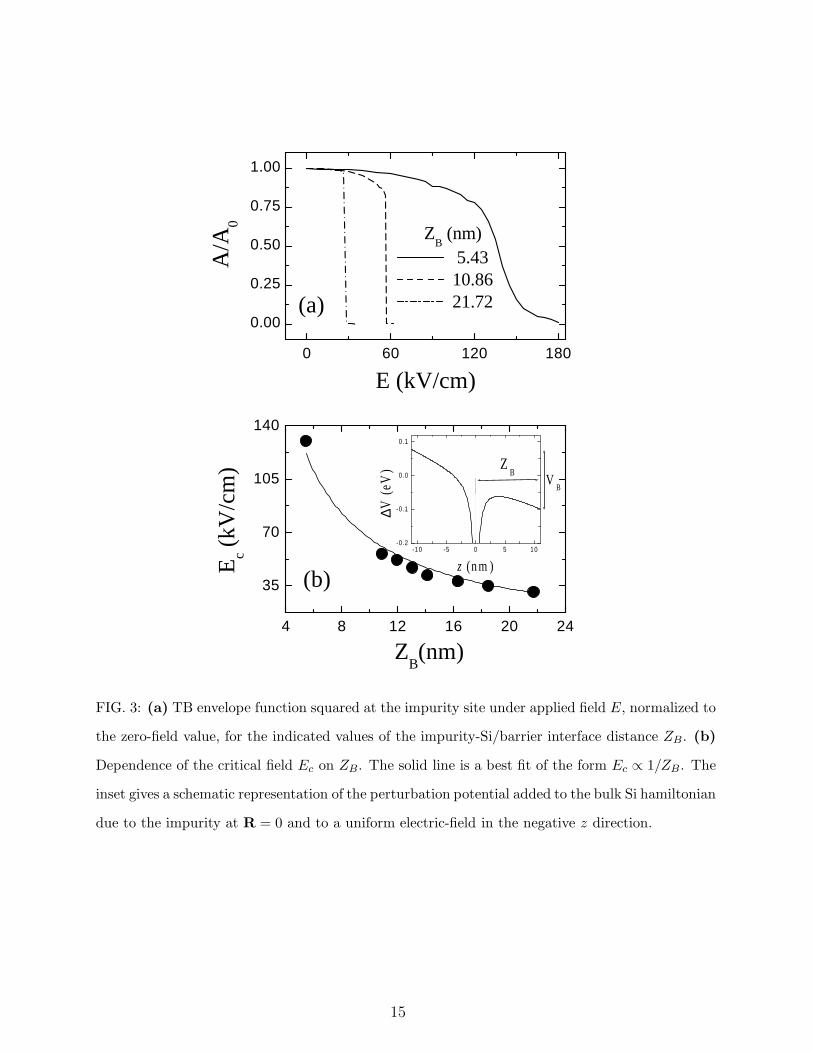
barrier material layer above the Si host1 (see inset in Fig. 3).
A description for the A-gate operations may be inferred from the behavior of the TB
envelope function squared at the impurity site under applied field E, normalized to the
zero-field value:
A/A0 = |ΨEEF (0)|2/|Ψ0
EF (0)|2 (9)
The notation here indicates that this ratio should follow a behavior similar to that for the
hyperfine coupling constants between the donor nucleus and electron with (A) and without
(A0) external field. Since the hyperfine interaction A is proportional to |Ψ(0)|2, and we
are using here the envelope rather than the full TB eigenfunctions, this equivalence is not
rigorous. The ratio in (9) is plotted in Fig. 3(a) for three values of the impurity depth
with respect to the Si/barrier interface. Calculations for ZB=10.86 nm were performed
with cubic supercells (L = 40), while for ZB= 5.43 and 21.72 nm tetragonal supercells
with Lx = Ly = 40 and Lz = 20 and 80 respectively were used. At small field values we
obtain a quadratic decay of A/A0 with E, in agreement with the perturbation theory results
6

for the hydrogen atom.18 At large enough fields, |ΨEEF (0)|2 becomes vanishingly small, and
the transition between the two regimes is qualitatively different according to ZB: For the
largest values of ZB we get an abrupt transition at a critical field Ec, while smaller ZB (e.g.
ZB = 5.43 nm) lead to a smooth decay, similar to the one depicted in Ref. 1. In this latter
case, we define Ec as the field for which the curve A/A0 vs E has an inflection point, where
A/A0 ∼ 0.5, thus Ec(5.43nm) = 130 kV/cm. We find that the decrease of Ec with ZB
follows a simple rule Ec ∝ 1/ZB, as given by the solid line in Fig. 3(b).
In order to analyze the different regimes illustrated in Fig. 3(a), we study the overall
behavior of the envelope squared profile along the z-axis,
ρ(z) =
2∑
s=1
∑
xsi ys
i
|ΨEEF (Rs
i )|2, (10)
where the first summation is over the two fcc sublattices, with Rsi corresponding to the
atomic sites in sublattice s, thus z labels each monolayer in the diamond structure, and
ρ(z) quantifies the z-projected charge distribution for the electron states under applied field
E. Fig. 4 gives ρ(z) for the electron ground state and also for the first excited state with
ZB = 10.86 nm as the applied field increases. Up to fields very close to Ec (∼ 53 kV/cm),
the ground state distribution retains essentially the bound donor character, with the elec-
tronic charge accumulating predominantly around the impurity (z = 0). For E > Ec we
observe an abrupt charge transfer towards the barrier, with some residual charge remaining
at the impurity site. The first excited state displays a complementary behavior, with charge
transfer from the barrier into the impurity region as E increases. The binding energies (en-
ergy eigenvalues relative to the bottom of the conduction band) are calculated here taking
into account the dependence of the conduction band edge under applied field. The binding
energies of the two lowest electron states are given in Fig. 5(a). Note that they cross at Ec.
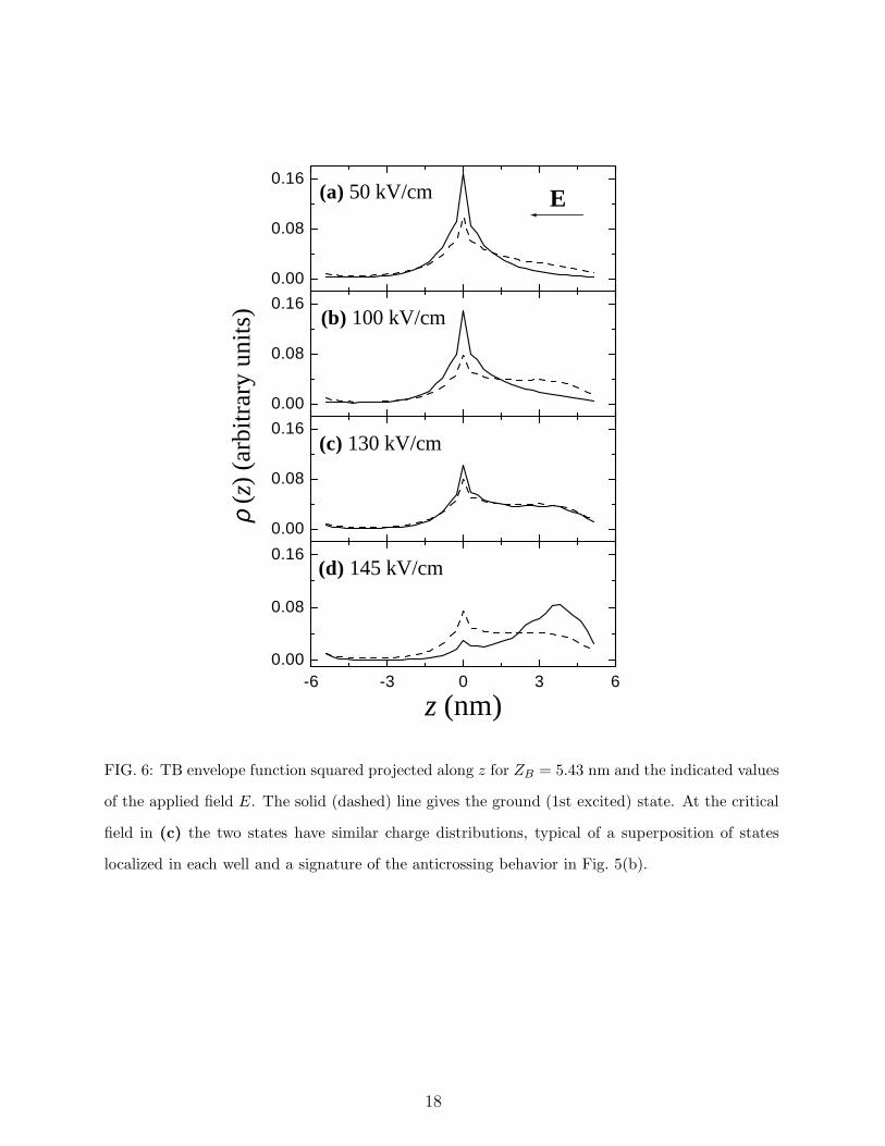
The binding energies of the two lowest eigenstates for ZB = 5.43 nm are presented in
Fig. 5(b). They do not cross, but rather display an anticrossing behavior, confirmed by the
corresponding doubled-peaked charge distributions in Fig. 6, with wavefunctions extending
over the attractive wells of the impurity and of the electric field potential. This is consistent
of eigenstates which are superpositions of bound states in each potential well. Note that for
E = Ec in Fig. 6(c), the two states have essentially the same charge distribution, as expected
at the anticrossing point. The anticrossing in Fig. 5(b) is such that for E < Ec the lines
giving the two states are essentially parallel, converging asymptotically at zero field to the
7

binding energies 45.6 meV, for the A1 ground state, and 32.4 meV for the first excited state.
This is very close to the experimental binding energy of the excited E (32.6 meV) and T2
(33.9 meV) states, which can not be individually resolved within our variational scheme.16
Note that this was independently obtained with the same value of the parameter U0, chosen
to fit the A1 state binding energy alone. Near and above Ec a typical 2-level anticrossing
behavior is obtained, with the excited state eventually merging into the conduction band at
E = 150 kV/cm.
The above results may be understood within a simple picture of the electron in a double
well potential, the first well being most attractive at the impurity site, V (R = 0) = −U0,
and the second well at the barrier interface, V (z = ZB) = −VB/2 = −|e|EZB neglecting
the Coulomb potential contribution (2) at the interface. An internal barrier separates the
two wells and, for a fixed E, this internal barrier height and width increase with ZB. Deep
donor positioning leads to a weaker coupling between the states localized at each well, even
close to level degeneracy, resulting the level crossing behavior illustrated in Fig.5(a). For
donor positioning closer to the interface the internal barrier gets weaker, enhancing the
coupling between levels localized in each well and leading to wavefunction superposition and
to the anticrossing behavior illustrated in Fig.5(b). The scaling of Ec with 1/ZB may also
be understood assuming that the critical field corresponds to the crossing of the ground
state energies of two wells: The Coulomb well and an approximately triangular well at the
barrier. Since the relative depths of the wells increases with EZB, and assuming that the
ground states energies are fixed with respect to each well’s depth, leads to the Ec ∝ 1/ZB
behavior.
IV. ADIABATIC PROCESSES DRIVEN BY AN UNIFORM ELECTRIC FIELD
Coherent manipulation of electrons by the A-gates requires that the switching time be-
tween different electron states be slow enough to guarantee adiabaticity of the process.
Instantaneous eigenstates of H(t) may thus be defined at any time t. In the present case,
we assume a linear increase of the external field from 0 to a maximum value Emax so that
H(t) = H(0) − |e|Emaxzt, with 0 < t < T , where T is the total switching time. A lower
8

bound for T is obtained from the adiabatic theorem,4,20 following Ref.10:
Ta =~|e|EmaxZB
g2min
, (11)
where gmin is the minimum gap between the two lowest electron states. In the anticrossing
case illustrated in Fig.5(b), we get gmin∼= 9.8 meV. Assuming that a totally ionized state
is required as the final state, we take Emax = 180 kV/cm, leading to Ta ∼ 0.5 ps. This
is a perfectly acceptable time for the operation of A-gates in spin-based Si QC, given the
relatively long electron spin coherence times (of the order of a few ms) in Si.21
As the impurity distance from the barrier increases, one eventually reaches the crossing
regime, when gmin → 0, meaning that Ta → ∞ and no adiabatic ionization is possible.
Ionization would still occur for E > Ec, but as a stochastic decay process from the first
excited state. From Fig. 3(a) we see that the A-gate might be used to partially reduce the
contact interaction, in the case of ZB = 10.86 nm to about 20% of its value at zero field. For
larger ZB the range for adiabatic variation in A/A0 is even smaller. Therefore ZB ∼ 5 nm
seems to be a favorable positioning for the donors, since it allows adiabatic reduction of
A/A0 to any desired final value, with this ratio varying smoothly from one (at E = 0) to
zero (for E = Emax ∼ 2Ec).
V. SUMMARY AND CONCLUSIONS
We have presented a TB study of donor levels in Si. The reliability of the TB approach
for the present study was verified by comparison of the TB and EMT envelope functions
as well as by the value predicted for the A1 − {E, T2} energy splitting in agreement with
experiment within our numerical accuracy. Previous TB studies of intermediate and shallow
impurity levels in semiconductors6,7,8 dealt with materials with band extrema at k = 0, and
the present results show that the oscillatory behavior of the wave function due to interference
effects in the plane-wave part of the Bloch wavefunctions, typical of degenerate band extrema
at k 6= 0, is well is well captured by the TB approach.
In the presence of an increasing uniform electric field, the donor states respond in different
ways according to the donor depth ZB below the Si/barrier interface. For deeply positioned
donors, i.e, for ZB >> a, b, where a and b are the Bohr radii for P in Si, abrupt ionization
occurs at a critical field Ec, while for ZB greater but of magnitude comparable to the Bohr
9

radii, a smooth electronic charge transfer from the donor site towards the barrier interface is
obtained, eventually leading to complete ionization. The different regimes were identified in
three ways: (i) From the decrease in electronic charge at the donor nucleus [Fig. 3(a)]. This
behavior implies an analogous dependence of the electron-nucleus hyperfine coupling con-
stant A as a function of the increasing external field. (ii) From charge distributions (Figs. 4
and 6), where the superposition of donor-like and barrier-like bound states is inhibited for
deeply positioned donors. (iii) From the behavior of the binding energies of the two lowest
electron states as the applied field increases (Fig. 5), changing from a level-crossing into an
anticrossing regime as ZB decreases. The donor excited states in the S-like manifold also
play a role in the anticrossing regime, as illustrated for E . Ec in Fig. 5(b).
The minimum gap gmin in the anticrossing regime is a key ingredient determining the
possibility of an adiabatic evolution of the electron state under the action of the A-gates.
Given that the product EcZB is approximately constant [see fit Fig. 3(b)], the adiabatic time
Ta in (11) is expected to depend very weakly in the product EmaxZB, assuming one aims at
complete ionization.3 Therefore Ta should not depend explicitly on ZB, but only implicitly
through 1/g2min. We have shown that for ZB ∼ 5 nm, i.e., about twice the largest Bohr
radius a in Eq. (7), electric field switching times smaller than 1 ps may be reached, which is
a favorable operation time given the long electronic spin coherence times in Si. If one aims
at a final state where only partial reduction of the electronic charge at the nucleus occurs1,2,
values of ZB of this order of magnitude are still the most convenient, since any final value
of the nuclear charge may be attained.
The Bloch phases interference behavior in the donor wavefunctions has been previously
shown to lead to oscillatory behavior of the exchange coupling between two donors,19 affect-
ing the two-qubit operations in exchange-based architectures in Si. We remark that such
oscillations are well captured in the TB wavefunctions, and that the present study demon-
strates that electric field control over single donor wavefunctions, such as proposed in A-gate
operations,1,2,3 do not present additional complications due to the Si band structure. The
only critical parameter is the donor positioning below the Si/barrier interface, which should
be chosen and controlled according to the physical criteria presented here.
10
Acknowledgments
We thank Daniel Loss and Bruce Kane for interesting discussions. We also thank Fabio
Ribeiro for useful suggestions. This work is partially supported by Brazilian agencies Con-
selho Nacional de Desenvolvimento Cientıfico e Tecnologico (CNPq), CAPES, Fundacao de
Amparo a Pesquisa do Rio de Janeiro (FAPERJ), Fundacao Universitaria Jose Bonifacio
(FUJB), PRONEX-MCT, and Instituto do Milenio de Nanociencias-CNPq.
1 B. E. Kane, Nature 393, 133 (1998)
2 R. Vrijen, E. Yablonovitch, K. Wang, W. H. Jiang, A. Balandin, V. Roychowdhury, T. Mor,
and D. DiVicenzo, Phys. Rev. A 62, 012306 (2000)
3 A. J. Skinner, M. E. Davenport, and B. E. Kane, Phys. Rev. Lett. 90, 087901 (2003)
4 A. Messiah, Quantum Mechanics (Dover-New York, 1999)
5 H. P. Hjalmarson, P. Vogl, D. J. Wolford, and J. D. Dow, Phys. Rev. Lett. 44, 810 (1980)
6 J. G. Menchero, R. B. Capaz, B. Koiller, and H. Chacham, Phys. Rev. B 59, 2722 (1999)
7 J. G. Menchero and T. B. Boykin, Phys. Rev. B 59, 8137 (1999)
8 A. S. Martins, J. G. Menchero, R. B. Capaz, and B. Koiller, Phys. Rev. B 65, 245205 (2002)
9 M. Graf and P. Vogl, Phys. Rev. B 51, 4940 (1995)
10 F. J. Ribeiro, R. B. Capaz, and Belita Koiller, Appl. Phys. Lett. 81, 2247 (2002)
11 J. M. Luttinger and W. Kohn, Phys. Rev 97, 869 (1955)
12 G. Klimeck, R. C. Bowen, T. B. Boykin, C. S.-Lazaro, T. A. Cwik, and A. Stoica, Superlattices
and Microstructures 27, 77 (2000)
13 R. B. Capaz, G. C. de Araujo, B. Koiller, and J. P. von der Weid, J,. Appl. Phys. 74, 5531
(1993)
14 T. G. Dargam, R. B. Capaz, and B. Koiller, Phys. Rev. B 56, 9625 (1997)
15 A. Baldereschi, Phys. Rev. B 1, 4673 (1970)
16 The six-fold degenerate S-like donor states in Si split into three components due to the tetrahe-
dral symmetry of the host: A non-degenerate ground state of A1 symmetry given in Eq. (6), an
excited triplet of symmetry T2 followed by an excited doublet of symmetry E. The TB treatment
adopted here correctly describes the symmetry and ordering of the states within this manifold
11

when full diagonalization of the TB Hamiltonian is performed. Within the variational scheme
we have not resolved the nearly-degenerate T2 and E levels, which are only 1.3 meV apart.
17 W. Kohn, Solid State Physics Series 5, Academic Press (1957)
18 L. I. Schiff, Quantum Mechanics, Third Edition - McGraw-Hill (chapter 8), (1968)
19 B. Koiller, X. Hu, and S. Das Sarma, Phys. Rev. Lett 88, 27903 (2002)
20 E. Farhi, J. Goldstone, S. Gutmann, J. Lapan, A. Lundgren, and D. Preda, Science 292, 472
(2001)
21 R. de Sousa and S. Das Sarma, cond-mat/0211467 (2003), to appear in PRB
12

0.8 1.0 1.2 1.4 1.6 1.8 2.0
0.0
0.2
0.4
0.6
28
35
42
49
56
63
UP
(b)
W(∆
min)
U0 (eV)
(a)
Eb (
meV
)
FIG. 1: (a) Binding energy of the ground impurity state as a function of the on-site perturbation
strength U0, obtained from the L → ∞ extrapolation ansatz. The dotted line indicates the value
U0 = UP that reproduces the experimental Si:P A1 state binding energy. (b) Calculated spectral
weight at the conduction band edge for the ground state. Notice that as the perturbation U0
becomes weaker, Eb approaches the EMT binding energy, while W does not approach 1.
13

1 2 3 4 5 6 7
0.0
2.0x10⁻⁴
4.0x10⁻⁴
6.0x10⁻⁴
1 2 3 4 5 6 7
0.0
4.0x10⁻⁴
8.0x10⁻⁴
1.2x10⁻³
1 2 3 4 5 6 7
0.0
2.0x10⁻⁴
4.0x10⁻⁴
6.0x10⁻⁴
R100
(nm)
R110
(nm)|ΨE
F|2 (ar
bitr
ary
unit
s)
R111
(nm)
FIG. 2: The dots give the TB envelope function squared for the lowest impurity state along three
high-symmetry directions. The lines are the corresponding effective mass |ψ|2 results. Note that
the TB approach captures the oscillations of the EMT wave function in the asymptotic region.
14
4 8 12 16 20 24
35
70
105
140
0 60 120 180
0.00
0.25
0.50
0.75
1.00
-10 -5 0 5 10-0 .2
-0 .1
0 .0
0 .1
VB
ZB
∆V (
eV)
z (n m )(b)
Ec (
kV/c
m)
ZB(nm)
(a)
ZB (nm) 5.43 10.86 21.72
A/A
0
E (kV/cm)
FIG. 3: (a) TB envelope function squared at the impurity site under applied field E, normalized to
the zero-field value, for the indicated values of the impurity-Si/barrier interface distance ZB . (b)
Dependence of the critical field Ec on ZB. The solid line is a best fit of the form Ec ∝ 1/ZB . The
inset gives a schematic representation of the perturbation potential added to the bulk Si hamiltonian
due to the impurity at R = 0 and to a uniform electric-field in the negative z direction.
15

-12 -8 -4 0 4 8 12
0.0
0.1
0.2
0.0
0.1
0.2
0.0
0.1
0.2
z (nm)
(b) 50 kV/cm
(c) 60 kV/cm
E
ρ ( z
) (a
rbit
rary
uni
ts)
(a) 0 kV/cm
FIG. 4: Tight binding envelope function squared projected along z for ZB = 10.86 nm and the
indicated values of the field E applied in the negative z direction. The solid (dashed) line gives
the donor ground (1st excited) state. Note in (b) and (c) the exchange among the ρ(z) for the
lowest energy states [ground] ↔ [excited] which occurs over a narrow rage of electric field increase,
a signature of the crossing behavior in Fig. 5(a).
16

50 52 54 5636
37
38
39
40
0 60 90 120 150 180
0
25
50
(a) ZB = 10.86 nm
Eb (
meV
)
E (kV/cm)
(b) ZB = 5.43 nm
Eb (
meV
)
E (kV/cm)
Electron ground state First excited state
FIG. 5: Calculated binding energies versus electric field intensity of the two lowest donor electron
states. (a) For ZB = 10.86 nm the energies reveal a crossing regime. (b) Anticrossing of the two
lowest electron states for ZB = 5.43 nm. The open symbols correspond the zero field calculated
values: 45.6 meV and 32.4 meV.
17
-6 -3 0 3 60.00
0.08
0.16
0.00
0.08
0.16
0.00
0.08
0.16
0.00
0.08
0.16
(b) 100 kV/cm
(a) 50 kV/cm
z (nm)
(c) 130 kV/cm
ρ ( z
) (a
rbit
rary
uni
ts)
E
(d) 145 kV/cm
FIG. 6: TB envelope function squared projected along z for ZB = 5.43 nm and the indicated values
of the applied field E. The solid (dashed) line gives the ground (1st excited) state. At the critical
field in (c) the two states have similar charge distributions, typical of a superposition of states
localized in each well and a signature of the anticrossing behavior in Fig. 5(b).
18
Copyright © 2022 FDOKUMEN