Probing Local Hydrogen Impurities in Quasi-Free-Standing Graphene
8
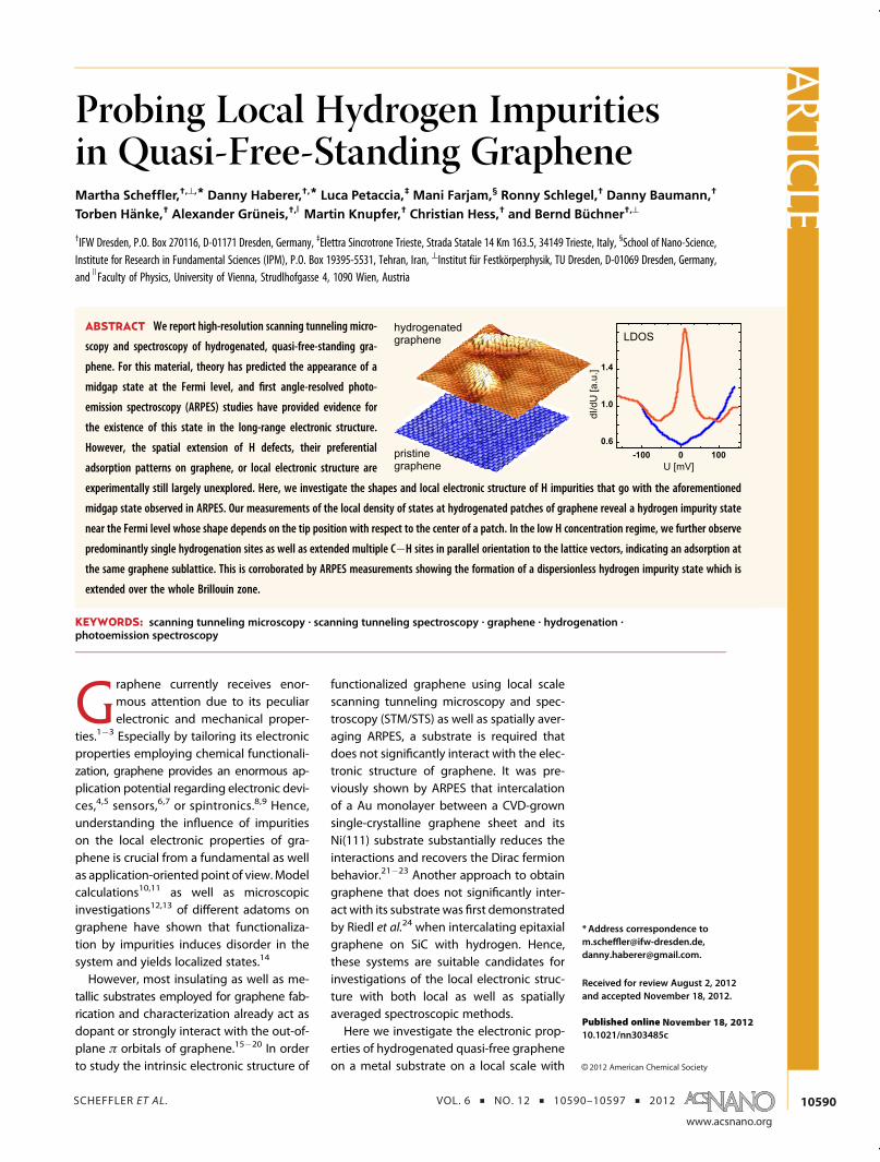
SCHEFFLER ET AL. VOL. 6 ’ NO. 12 ’ 10590–10597 ’ 2012 www.acsnano.org 10590 November 18, 2012 C 2012 American Chemical Society Probing Local Hydrogen Impurities in Quasi-Free-Standing Graphene Martha Scheffler, †,^, * Danny Haberer, †, * Luca Petaccia, ‡ Mani Farjam, § Ronny Schlegel, † Danny Baumann, † Torben Ha ¨ nke, † Alexander Gru ¨ neis, †, ) Martin Knupfer, † Christian Hess, † and Bernd Bu ¨ chner †,^ † IFW Dresden, P.O. Box 270116, D-01171 Dresden, Germany, ‡ Elettra Sincrotrone Trieste, Strada Statale 14 Km 163.5, 34149 Trieste, Italy, § School of Nano-Science, Institute for Research in Fundamental Sciences (IPM), P.O. Box 19395-5531, Tehran, Iran, ^ Institut für Festkörperphysik, TU Dresden, D-01069 Dresden, Germany, and ) Faculty of Physics, University of Vienna, Strudlhofgasse 4, 1090 Wien, Austria G raphene currently receives enor- mous attention due to its peculiar electronic and mechanical proper- ties. 13 Especially by tailoring its electronic properties employing chemical functionali- zation, graphene provides an enormous ap- plication potential regarding electronic devi- ces, 4,5 sensors, 6,7 or spintronics. 8,9 Hence, understanding the influence of impurities on the local electronic properties of gra- phene is crucial from a fundamental as well as application-oriented point of view. Model calculations 10,11 as well as microscopic investigations 12,13 of different adatoms on graphene have shown that functionaliza- tion by impurities induces disorder in the system and yields localized states. 14 However, most insulating as well as me- tallic substrates employed for graphene fab- rication and characterization already act as dopant or strongly interact with the out-of- plane π orbitals of graphene. 1520 In order to study the intrinsic electronic structure of functionalized graphene using local scale scanning tunneling microscopy and spec- troscopy (STM/STS) as well as spatially aver- aging ARPES, a substrate is required that does not significantly interact with the elec- tronic structure of graphene. It was pre- viously shown by ARPES that intercalation of a Au monolayer between a CVD-grown single-crystalline graphene sheet and its Ni(111) substrate substantially reduces the interactions and recovers the Dirac fermion behavior. 2123 Another approach to obtain graphene that does not significantly inter- act with its substrate was first demonstrated by Riedl et al. 24 when intercalating epitaxial graphene on SiC with hydrogen. Hence, these systems are suitable candidates for investigations of the local electronic struc- ture with both local as well as spatially averaged spectroscopic methods. Here we investigate the electronic prop- erties of hydrogenated quasi-free graphene on a metal substrate on a local scale with * Address correspondence to m.scheffl[email protected], [email protected]. Received for review August 2, 2012 and accepted November 18, 2012. Published online 10.1021/nn303485c ABSTRACT We report high-resolution scanning tunneling micro- scopy and spectroscopy of hydrogenated, quasi-free-standing gra- phene. For this material, theory has predicted the appearance of a midgap state at the Fermi level, and first angle-resolved photo- emission spectroscopy (ARPES) studies have provided evidence for the existence of this state in the long-range electronic structure. However, the spatial extension of H defects, their preferential adsorption patterns on graphene, or local electronic structure are experimentally still largely unexplored. Here, we investigate the shapes and local electronic structure of H impurities that go with the aforementioned midgap state observed in ARPES. Our measurements of the local density of states at hydrogenated patches of graphene reveal a hydrogen impurity state near the Fermi level whose shape depends on the tip position with respect to the center of a patch. In the low H concentration regime, we further observe predominantly single hydrogenation sites as well as extended multiple CH sites in parallel orientation to the lattice vectors, indicating an adsorption at the same graphene sublattice. This is corroborated by ARPES measurements showing the formation of a dispersionless hydrogen impurity state which is extended over the whole Brillouin zone. KEYWORDS: scanning tunneling microscopy . scanning tunneling spectroscopy . graphene . hydrogenation . photoemission spectroscopy ARTICLE
-
Upload
ucberkeley -
Category
Documents
-
view
0 -
download
0
Transcript of Probing Local Hydrogen Impurities in Quasi-Free-Standing Graphene
SCHEFFLER ET AL. VOL. 6 ’ NO. 12 ’ 10590–10597 ’ 2012
www.acsnano.org
10590
November 18, 2012
C 2012 American Chemical Society
Probing Local Hydrogen Impuritiesin Quasi-Free-Standing GrapheneMartha Scheffler,†,^,* Danny Haberer,†,* Luca Petaccia,‡ Mani Farjam,§ Ronny Schlegel,† Danny Baumann,†
Torben Hanke,† Alexander Gruneis,†, ) Martin Knupfer,† Christian Hess,† and Bernd Buchner†,^
†IFW Dresden, P.O. Box 270116, D-01171 Dresden, Germany, ‡Elettra Sincrotrone Trieste, Strada Statale 14 Km 163.5, 34149 Trieste, Italy, §School of Nano-Science,Institute for Research in Fundamental Sciences (IPM), P.O. Box 19395-5531, Tehran, Iran, ^Institut für Festkörperphysik, TU Dresden, D-01069 Dresden, Germany,and )Faculty of Physics, University of Vienna, Strudlhofgasse 4, 1090 Wien, Austria
Graphene currently receives enor-mous attention due to its peculiarelectronic and mechanical proper-
ties.1�3 Especially by tailoring its electronicproperties employing chemical functionali-zation, graphene provides an enormous ap-plication potential regarding electronic devi-ces,4,5 sensors,6,7 or spintronics.8,9 Hence,understanding the influence of impuritieson the local electronic properties of gra-phene is crucial from a fundamental as wellas application-oriented point of view.Modelcalculations10,11 as well as microscopicinvestigations12,13 of different adatoms ongraphene have shown that functionaliza-tion by impurities induces disorder in thesystem and yields localized states.14
However, most insulating as well as me-tallic substrates employed for graphene fab-rication and characterization already act asdopant or strongly interact with the out-of-plane π orbitals of graphene.15�20 In orderto study the intrinsic electronic structure of
functionalized graphene using local scalescanning tunneling microscopy and spec-troscopy (STM/STS) as well as spatially aver-aging ARPES, a substrate is required thatdoes not significantly interact with the elec-tronic structure of graphene. It was pre-viously shown by ARPES that intercalationof a Au monolayer between a CVD-grownsingle-crystalline graphene sheet and itsNi(111) substrate substantially reduces theinteractions and recovers the Dirac fermionbehavior.21�23 Another approach to obtaingraphene that does not significantly inter-act with its substrate was first demonstratedby Riedl et al.24 when intercalating epitaxialgraphene on SiC with hydrogen. Hence,these systems are suitable candidates forinvestigations of the local electronic struc-ture with both local as well as spatiallyaveraged spectroscopic methods.Here we investigate the electronic prop-
erties of hydrogenated quasi-free grapheneon a metal substrate on a local scale with
* Address correspondence [email protected],[email protected].
Received for review August 2, 2012and accepted November 18, 2012.
Published online10.1021/nn303485c
ABSTRACT We report high-resolution scanning tunneling micro-
scopy and spectroscopy of hydrogenated, quasi-free-standing gra-
phene. For this material, theory has predicted the appearance of a
midgap state at the Fermi level, and first angle-resolved photo-
emission spectroscopy (ARPES) studies have provided evidence for
the existence of this state in the long-range electronic structure.
However, the spatial extension of H defects, their preferential
adsorption patterns on graphene, or local electronic structure are
experimentally still largely unexplored. Here, we investigate the shapes and local electronic structure of H impurities that go with the aforementioned
midgap state observed in ARPES. Our measurements of the local density of states at hydrogenated patches of graphene reveal a hydrogen impurity state
near the Fermi level whose shape depends on the tip position with respect to the center of a patch. In the low H concentration regime, we further observe
predominantly single hydrogenation sites as well as extended multiple C�H sites in parallel orientation to the lattice vectors, indicating an adsorption at
the same graphene sublattice. This is corroborated by ARPES measurements showing the formation of a dispersionless hydrogen impurity state which is
extended over the whole Brillouin zone.
KEYWORDS: scanning tunneling microscopy . scanning tunneling spectroscopy . graphene . hydrogenation .photoemission spectroscopy
ARTIC
LE

SCHEFFLER ET AL. VOL. 6 ’ NO. 12 ’ 10590–10597 ’ 2012
www.acsnano.org
10591
STM and STS in combinationwith ARPES. We show thatour starting material, graphene on Au, exhibits a highcrystalline quality with no observable defects or ad-sorbates on the local scale, which is a crucial precondi-tion for studies of artificial impurities. We probe thetopography as well as the local density of states (LDOS)with STM/STS in subnanometer resolution and findpronounced impurity states at hydrogenation siteswith position-dependent shapes and widths. In con-trast to measurements of graphene on Ir(111) withstronger substrate interaction, where a full hydrogena-tion of the graphene was shown,25 we focus in thiswork onwell-isolated hydrogenated sites. The compar-ison of shape and size of the obtained hydrogenatedpatches with density functional based tight bindingmethod (DFTB) calculations suggests that atomic hy-drogen adsorbs on graphene in the low concentrationregime giving rise to single and extended double ortriple C�H sites with spatial orientations that followthat of a meta configuration. The studies of the localelectronic structure of hydrogenated graphene arecorroborated by complementary ARPES measure-ments. We demonstrate the formation of a hydrogenimpurity state across the Brillouin zone and furtherdiscuss the p-type doping induced by hydrogen im-purities on graphene.
RESULTS AND DISCUSSION
Figure 1a shows a typical topographic image of as-produced graphene on a Ni(111) substrate. The insetrepresents the fast Fourier transform (FFT) of the imagefrom which we determine the lattice constant withingiven accuracy to 2.4((0.1) Å (consistent with theexpected value for graphene of 2.46 Å). The graphenelayer covers the substrate homogeneously and acrossstep edges as it is expected from the CVD growth onsingle-crystalline substrates.26�28 Furthermore, we donot observe significant lattice distortions, defects, oradsorbates neither on the local atomic scale (50 nm �50 nm) nor on larger areas (shown in Figure S1 of theSupporting Information) which outlines the high qual-ity of the obtained graphene. However, its electronicstructure is strongly modified by the Ni substrate dueto hybridization29,30 which in turn affects the spectro-scopic measurements. Figure 1b depicts a typical STSspectrum of graphene/Ni(111) obtained at 300 K. Therecorded LDOS exhibits two prominent features ataround �400 mV and þ450 mV bias voltage, whichare related to the spin-split band edges of the Ni bandstructure and, thus, the electronic structure of thesubstrate rather than that of graphene.31,32 In orderto investigate the local electronic properties of gra-phene, and subsequently those of hydrogen adsor-bates, a liberation from the Ni substrate is crucial.The intercalation of one monolayer (ML) Au effec-
tively decouples graphene electronically from the Nisubstrate21�23 and induces a Moiré superstructure in
topography images due to a lattice mismatch betweenAu and graphene22,23 (further topographic images oflarger areas for graphene/Au are shown in Figure S2 ofthe Supporting Information). In Figure 1c, a region ofthe sample with the superstructure after Au intercala-tion is shown. The FFT in the inset indicates thehexagonal graphene lattice as well as the additionalreflexes of the Moiré pattern, which relate to a goldlattice constant of 27.4 Å, in agreement with previousvalues.22,23 The superstructure is also observed forlarger sample areas as well as in low energy electrondiffraction (see Supporting Information) and thus in-dicates a fully developed Au intercalation.The electronic properties of the graphene/Ni(111)
system are strongly influenced by the Au intercalationprocess, as it shifts the chemical potential of grapheneby 2 eV and recovers the Dirac fermion behavior ofcharge carriers near the Fermi level.22 The dI/dU curvein Figure 1d follows the typical V shape as expectedfor the graphene DOS from band structure calcula-tions.33,34 For graphene on top of 1 ML Au, we identifythe Dirac point at theminimum of the spectrum. In our
Figure 1. (a) Atomically resolved topography image of as-produced graphene on Ni(111). No significant defects on allinvestigated areas were observed. Inset: FFT, spots corre-spond to lattice constant of 2.4 Å (I = 0.8 nA, U =�250 mV).(b) dI/dU spectrum (average over 8 � 8 spectroscopic mapof 5 nm �5 nm) of graphene/Ni(111). Shoulders at around�400mVand400mV refer to theNi electronic structure andprevent an investigation of bare graphene (I = 0.25 nA,U = �600 mV, Umod = 10 mV, T = 300 K). (c) Topography ofgraphene intercalated with 1 ML Au leading to a latticemismatch induced Moiré pattern. Inset: FFT, outer spotscorrespond to a lattice constant of 2.4 Å. Inner spotsdepicted in the zoomed image are related to the Moirépatternwitha lattice constantof27.4Å (I=0.5nA,U=�100mV,T=20 K). (d) dI/dU curves of graphene after Au intercalation,averaged over a 5 � 5 spectroscopic map of 5 nm � 5 nm.The quasi-free-standing graphene exhibits a nearly linear,symmetric shape in the LDOS with a minimum at the Fermienergy (I = 0.5 nA, U = �100 mV, Umod = 4 mV, T = 20 K).Inset: larger bias scale, averaged over 10 single-pointspectra (I = 0.5 nA, U = �400 mV, Umod = 4 mV, T = 20 K).
ARTIC
LE

SCHEFFLER ET AL. VOL. 6 ’ NO. 12 ’ 10590–10597 ’ 2012
www.acsnano.org
10592
system, we observe a slight shift of the Dirac point topositive bias voltage by about 4mV, which is within theresolution limit. Hence, the intrinsic doping level ofgraphene in the investigated system is close to chargeneutrality, which is in agreement with ARPES measure-ments22 and similar by trend to previous works forquasi-free graphene on a graphite substrate.35 As canbe seen on the large bias scale in the inset, the featuresat �400 mV and þ450 mV in the dI/dU curves, origi-nating from the Ni(111) substrate, are now sufficientlyreduced, especially the plateau at positive bias voltage.We also do not observe a significant variation in thedI/dU curves when comparing spectra obtained frombright and dark regions of the Moiré pattern (seeSupporting Information). Hence, graphene on 1 MLAuprovides a suitable base to study the local electronicproperties of adsorbed impurities such as atomichydrogen, which is presented in the following.Figure 2a shows a large area topography scan of
graphene over several terraces after hydrogenation for10 s at 5 � 10�9 mbar. In addition to the honeycomblattice, we observe randomly distributed but yet isolatedbright spots, which are assigned to H impurities,36�38
and further indicate a low concentration of adsorbates.From the large area scans, we estimate a hydrogencoverage of approximately 0.02%. The Moiré super-structure detected in the FFT (inset) is slightly diffusedue to the step edges of the substrate and the pre-sence of H impurities which interfere with the latticesymmetry of graphene. Figure 2b,c contains atomic-resolution topography images of the hydrogenationsites, which are representative for all investigated areason the sample. Owing to the highmobility of hydrogenimpurities, the mapping of the hydrogen spots with anSTM tip is only possible under particular conditions,such as low bias and slow scanning speed. With the
chosen scanning parameters, wemeasure very close tothe emerging H impurity state (see Figure 3a) andprobe therefore the spatial extension of this state.The structural relaxation of the lattice leads to a strongphysical as well as electronic distortion of nearbybonds, which is observed in the high-resolution STMimages, where the bonding partner of the impurity insublattice A results in a localization of the impuritystate in sublattice B and at the impurity atom.11,39 Wehave investigated several different hydrogenation siteson the sample and find two predominant shapes in theatomically resolved scans (additional topographies ofhydrogenation sites from different regions on thesample are shown in Figure S3 of the SupportingInformation). Some patches are confined and have arather circular or sometimes a triangular form (Figure 2b),while others exhibit a more elongated shape (Figure 2c).Hence, the observed structures may correspond to thetheoretically predicted appearance of single site39 aswell as double site impurities40,41 and are further-more similar to previously reported H monomerand (extended) dimer structures on top of grapheneon SiC.38
In order to assign the observed topographic shapes,we have performed DFTB-based calculations of thecharge density distribution for single and double Himpurity sites. In Figure 2e,f, we show the expectedspatial extension of a single and a double site in ametaconfiguration, which implies H adsorption on the samegraphene sublattice as indicated in the sketch ofFigure 2d. The blue parts correspond to excess electrondensity and are therefore comparable with a high STMintensity in the negative bias range. According to thecalculation, a single hydrogen impurity introduces a(D3h) symmetry of the wave function in close vicinity ofthe C�H site, which induces a triangular pattern in the
Figure 2. (a) Graphene onAu after controlled hydrogen exposure. TheMoiré patternwith a corresponding lattice constant of27 Å is also found in the FFT (inset). Bright spots are hydrogen adsorption sites (I = 0.2 nA, U = �50 mV, T = 20 K). (b,c)Atomically resolved topography images near hydrogen adsorption sites (I= 0.5 nA,U=�20mV, T=20 K). On the bright spots,the graphene lattice appears distorted. Dashed lines correspond to impurity shapes suggested by DFTB-based modelcalculations. (d) Sketch of double hydrogenation sites employed in the calculation. Calculated charge density distributions,where blue/red color shows a( isosurface, for (e) a single C�H site and (f) a double C�H site inmeta configuration describingthe experimental topographies in (b) and (c), respectively.
ARTIC
LE
SCHEFFLER ET AL. VOL. 6 ’ NO. 12 ’ 10590–10597 ’ 2012
www.acsnano.org
10593
charge density distribution. It becomes nearly circularwith a size of about 10 lattice constants at largerdistances from the C�H bond. The spatial extensionas well as the shape of the calculated charge densitydistribution for a single C�H site are in good agree-ment with the single protrusion in the STM topo-graphy, shown in Figure 2b. The elongated shapes,representatively shown in Figure 2c, point at firsttoward double C�H sites. In this case, three pos-sible configurations, illustrated in Figure 2d, ortho,meta, and para which correspond to additional hydro-genation of nearest, next-nearest, and third-nearestneighbor C atoms, are conceivable. However, in ourcalculations, only a meta configuration as shown inFigure 2f gives rise to a spatial extension of the chargedensity along the zigzag edges of graphene overseveral lattice constants. When comparing the exten-sion of the calculated charge density with that of theobserved elongated protrusions, we find a differencein length of about three to four lattice constants.Hence, it is likely that the elongated protrusions consistof extended double or even triple hydrogenation sitesoriented parallel to the lattice vectors in a meta con-figuration. The spacing between individual H atoms insuch a configuration can be a few lattice constants, sothat the high absorption barrier for a meta configuration
can be reduced.41 Nevertheless, we expect for thesesites an emerging impurity state, as the orientationparallel to the lattice vectors suggests a hydrogenationof the same sublattice. This breaks, like single C�Hsites, the symmetry between A and B carbon atomsand leads to the formation of a band gap as waspreviously shown by ARPES for higher H/C ratios andtheoretical calculations.9,23
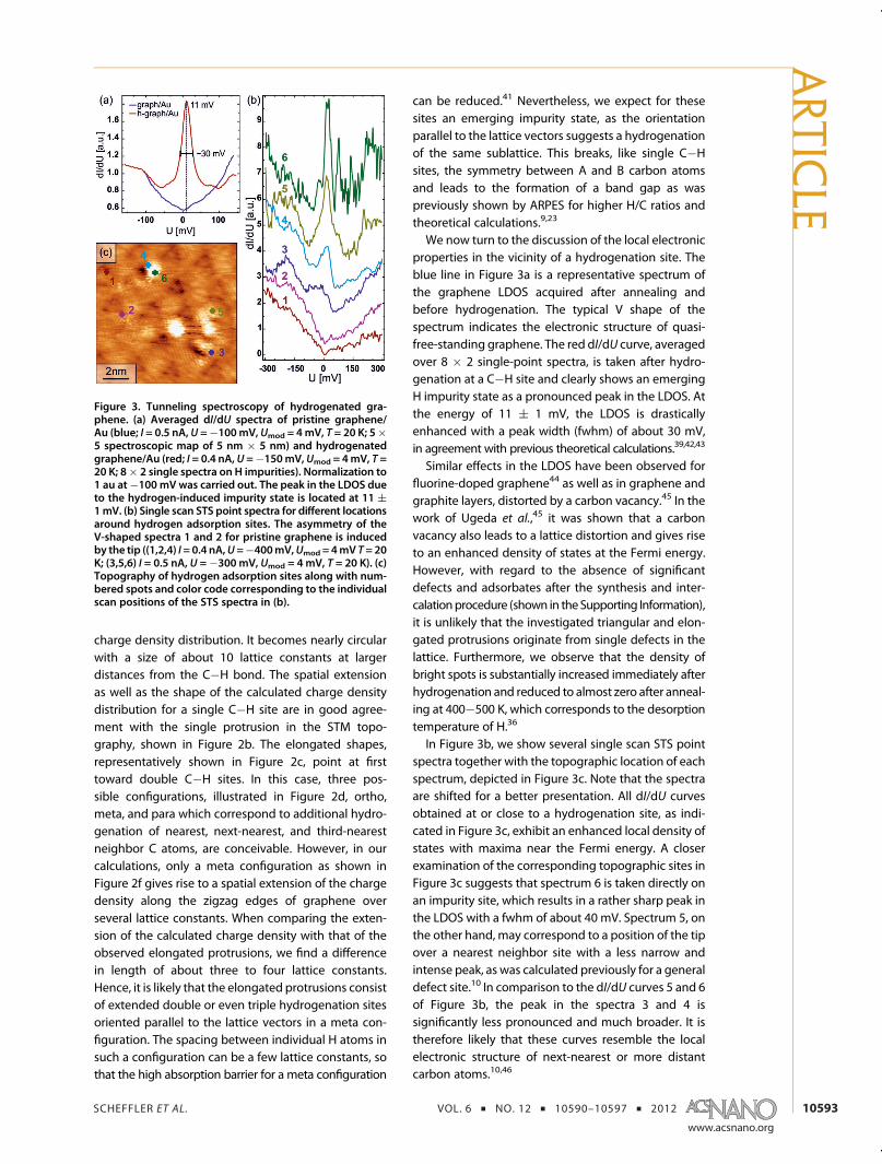
We now turn to the discussion of the local electronicproperties in the vicinity of a hydrogenation site. Theblue line in Figure 3a is a representative spectrum ofthe graphene LDOS acquired after annealing andbefore hydrogenation. The typical V shape of thespectrum indicates the electronic structure of quasi-free-standing graphene. The red dI/dU curve, averagedover 8 � 2 single-point spectra, is taken after hydro-genation at a C�H site and clearly shows an emergingH impurity state as a pronounced peak in the LDOS. Atthe energy of 11 ( 1 mV, the LDOS is drasticallyenhanced with a peak width (fwhm) of about 30 mV,in agreement with previous theoretical calculations.39,42,43
Similar effects in the LDOS have been observed forfluorine-doped graphene44 as well as in graphene andgraphite layers, distorted by a carbon vacancy.45 In thework of Ugeda et al.,45 it was shown that a carbonvacancy also leads to a lattice distortion and gives riseto an enhanced density of states at the Fermi energy.However, with regard to the absence of significantdefects and adsorbates after the synthesis and inter-calationprocedure (shown in theSupporting Information),it is unlikely that the investigated triangular and elon-gated protrusions originate from single defects in thelattice. Furthermore, we observe that the density ofbright spots is substantially increased immediately afterhydrogenation and reduced to almost zero after anneal-ing at 400�500 K, which corresponds to the desorptiontemperature of H.36
In Figure 3b, we show several single scan STS pointspectra together with the topographic location of eachspectrum, depicted in Figure 3c. Note that the spectraare shifted for a better presentation. All dI/dU curvesobtained at or close to a hydrogenation site, as indi-cated in Figure 3c, exhibit an enhanced local density ofstates with maxima near the Fermi energy. A closerexamination of the corresponding topographic sites inFigure 3c suggests that spectrum 6 is taken directly onan impurity site, which results in a rather sharp peak inthe LDOS with a fwhm of about 40 mV. Spectrum 5, onthe other hand, may correspond to a position of the tipover a nearest neighbor site with a less narrow andintense peak, as was calculated previously for a generaldefect site.10 In comparison to the dI/dU curves 5 and 6of Figure 3b, the peak in the spectra 3 and 4 issignificantly less pronounced and much broader. It istherefore likely that these curves resemble the localelectronic structure of next-nearest or more distantcarbon atoms.10,46
Figure 3. Tunneling spectroscopy of hydrogenated gra-phene. (a) Averaged dI/dU spectra of pristine graphene/Au (blue; I = 0.5 nA,U =�100mV, Umod = 4mV, T = 20 K; 5�5 spectroscopic map of 5 nm � 5 nm) and hydrogenatedgraphene/Au (red; I = 0.4 nA,U =�150mV,Umod = 4mV, T =20 K; 8� 2 single spectra on H impurities). Normalization to1 au at�100 mV was carried out. The peak in the LDOS dueto the hydrogen-induced impurity state is located at 11 (1mV. (b) Single scan STS point spectra for different locationsaround hydrogen adsorption sites. The asymmetry of theV-shaped spectra 1 and 2 for pristine graphene is inducedby the tip ((1,2,4) I=0.4 nA,U=�400mV,Umod = 4mV T=20K; (3,5,6) I = 0.5 nA, U =�300 mV, Umod = 4 mV, T = 20 K). (c)Topography of hydrogen adsorption sites along with num-bered spots and color code corresponding to the individualscan positions of the STS spectra in (b).
ARTIC
LE

SCHEFFLER ET AL. VOL. 6 ’ NO. 12 ’ 10590–10597 ’ 2012
www.acsnano.org
10594
The sharp peak in the LDOS at an impurity siteprovides strong evidence for a well-defined state with-out significant dispersion in k-space. However, withSTM being a method of choice for unraveling the localelectronic properties, we further employ ARPES toinvestigate the long-range electronic structure ink-space with high resolution. Since ARPES providesinformation only on the occupied states of the elec-tronic structure, it is hardly possible to identify theimpurity state located slightly above the Dirac pointenergy. Hence, we dope graphene with additionalelectrons from potassium in order to shift the Fermilevel into the conduction band. The H impurity statecan then be directly observed with ARPES, as we haveshown previously.46
In Figure 4a, a 2D photoemission intensity map at EFof fully potassium-doped graphene is shown. The Fermisurface contour, obtained from photoemission inten-sity maxima, exhibits a typical trigonally warped shapesimilar to KC8.
47 From the enclosed k-space area, weobtain a doping of 0.061(3) extra electrons per gra-phene unit cell which corresponds to a shift of theDirac point with respect to EF of about 1.3 eV (for ARPESspectra along Γ�K�M direction, see Supporting Infor-mation), in agreement with previous results for KC8
47
and graphene on Ir(111).48 In Figure 4b, we depict theintegrated photoemission intensity as a function of the
binding energy. The corresponding segments in the2D Brillouin zone along which the integration is carriedout are indicated in Figure 4a. The rather flat andfeatureless curve, obtained from a region beyond theπ* cone, is related to the electronic structure of the Aumonolayer below graphene. In contrast, the cut throughthe K-point exhibits an increased spectral weight nearEF originating from the occupied π*-band.After exposing K-doped graphene to atomic hydro-
gen, we observe a reduction of the Fermi surface area,shown in Figure 4c, which is equivalent to a doping of0.045(2) extra electrons per unit cell. This implies holedoping induced by the bonding hydrogen, in agree-ment with previous results.46,49 Assuming one hole perattached H atom,49 we obtain an average hydrogenconcentration of 0.8( 0.2%, which corresponds to thecritical concentration for the formation of a hydrogen-derived impurity state in the long-range electronicproperties.46 Cutting the Fermi surface map at thesame positions as in Figure 4a, we obtain the EDCsfor hydrogenated graphene, shown in Figure 4d. Bothcurves clearly illustrate the manifestation of the Himpurity state in the vicinity of the Dirac point. Forboth cuts, within and outside the π* cone, the hydro-gen-related feature is found at the same energy, whichsuggests, in agreement with our previous results,46 theabsence of any dispersion and extension of this stateacross the Brillouin zone. The impurity state observedin ARPES has a width of ∼280 meV (fwhm) and issubstantially broader than in the local STS spectra,which is probably attributed to the spatial insensitivityof ARPES. Hence, we observe all contributions fromneighboring as well as double C�H sites10,11 in thespectra.
CONCLUSIONS
We have demonstrated by STM/STS that in situ
synthesized graphene/Au/Ni(111) is sufficiently welldecoupled from the underlying Ni to serve as startingsubstrate for investigations of chemical functionaliza-tion. Furthermore, the system is, with its locally lowintrinsic graphene intrinsic doping level close to neu-trality, comparable with graphene on graphite35 andthus a perfect basis to investigate the electronic prop-erties of impurities on an atomic scale. By controlledhydrogenation, we have shown, with both local STS aswell as ARPES measurements, the emergence of ahydrogen impurity state in close vicinity to the Diracpoint and the propagation of the state over the wholeBrillouin zone. Local measurements of the topographyof the hydrogen adsorption sites have shown charac-teristic patterns, which have been related to simula-tions of single and double impurities on graphene. Forthe observed elongated structures, we have suggestedthe presence of extended double or triple C�H siteswhich are oriented in a meta configuration, indicatinga hydrogenation of the same sublattice. The spectra we
Figure 4. (a) Fermi surface map of fully K-doped graphenealong with the Fermi surface contour (black dots). Dashedlines indicate cutting directions for the EDCs in (b). Whitesolid lines mark the boundaries of the Brillouin zone. (b)EDCs along the Γ�K�M direction (gray) and outside theFermi surface (black). ED indicates the position of the Diracpoint. (c) Fermi surface map after hydrogenation for 10 minat 1� 10�8 mbar. The dashed contour represents the Fermisurface of fully K-doped graphene from (a). (d) EDCsobtained from integrating along the corresponding dashedlines in (c), showing the emerging dispersionless H impuritystate in the BZ.
ARTIC
LE

SCHEFFLER ET AL. VOL. 6 ’ NO. 12 ’ 10590–10597 ’ 2012
www.acsnano.org
10595
have obtained on a local impurity site support thetheoretical model for the bonding of the H adatom tothe graphene lattice and the induced change ofthe electronic properties on nearby lattice sites.11,39 Ina future work, spin-polarized STS on these samplesis suggested in order to experimentally prove the
theoretically predicted spin-splitting.42 Also for vacan-cies in graphene, magnetic changes in the LDOS areexpected.14,50 Our results based on graphene/Au pro-vide a suitable basis for further studies of local mag-neticmoments and spin-resolved studies at impurity ordefect sites.
EXPERIMENTAL METHODSWe prepared pristine monolayer graphene samples in situ
under ultrahigh vacuum conditions by chemical vapor deposi-tion on Ni(111) thin films, epitaxially grown on W(110).51 Here-after, one monolayer (ML) of Au was deposited on graphenefollowed by intercalation into the graphene/Ni interface byannealing at 500�600 �C.21�23 Hydrogenation of graphenewas performed at room temperature by exposing the sampleto a beam of atomic H that was produced by cracking H2 at2800 K in a W capillary using a pressure of 5 � 10�9 mbar for10�20 s. In order to prevent a full loss of hydrogenmonomers atroom temperature,52 the sample was transferred immediatelyafter hydrogen exposure to the STM chamber. Further details onsample preparation and hydrogenation are given in previousworks.23,53
We used a home-built variable-temperature STM for investi-gation of the samples. The temperatures during STM measure-ments were 300 K for graphene/Ni(111) or 20 K for graphene/Au, and the pressure in the UHV preparation chamber wasbetter than 2 � 10�9 mbar, whereas during data acquisition at20 K, the base pressure in the STM chamber was e4 � 10�10
mbar. The imaging of graphene was done over a wide biasrange in positive and negative voltages, but most of the imagesshown here were taken at similar parameters of I = (0.2...0.5) nAand U =�(40...500) mV. Calibration of the STS spectra, shown inthis work, was achieved by scanning a Au(111) thin film onmicaprior to and after measuring graphene. Processing of thetopographic images was carried out with the WSxM software.54
ARPESmeasurements were performed at the BaDElPh beamlineof the Elettra synchrotron facility in Trieste (Italy).55 The spectrawere acquired at photon energies of 29 eV with the sample at50 K and a base pressure better than 8 � 10�11 mbar. Theangular and energy resolution were set to 0.15� and 15 meV,respectively. Doping of graphene was achieved in situ by Kevaporation from commercial SAES getters followed by thermalannealing to establish a KC8 stoichiometry.46 Hydrogenationwas carried out with the same H source employed for functio-nalization in the STM setup but at a pressure of 1 � 10�8 mbarfor 10 min, while the sample was kept at 50 K.Calculations of the charge density were carried out with the
density functional based tight binding (and more) (DFTBþ)simulation package56,57 and the visualization by VMD.58 A unitcell of 450 carbon atoms was applied and the difference in thetwo charge densities of a pristine and hydrogenated graphenelattice simulated. Blue color in the simulated images shows apositive isosurface and therefore the excess electron density,which is approximately comparable with a high STM intensity inthe negative bias range.
Conflict of Interest: The authors declare no competingfinancial interest.
Acknowledgment. This work has been funded by the DFGthrough the Research Unit FOR 1154 (Grant No. HA6037/1) andthe Graduate School GRK 1621. D.H., A.G., and M.K. acknowl-edge DFG Grant No. GR 3708/1-1. A.G. acknowledges an APARTfellowship from the Austrian Academy of Sciences. D.H. and A.G.acknowledge funding from the EuropeanCommunity's SeventhFramework Program (FP7/2007-2013) under grant agreement226716 for their stay at the Elettra synchrotron. D.H., L.P., and A.G. thank D. Lonza for technical assistance during the ARPESmeasurements. D.H. and M.S. thank R. Schönfelder, R. Hübel, S.Leger, and F. Herold for technical support. VMD was developedby the Theoretical and Computational Biophysics Group in the
Beckman Institute for Advanced Science and Technology at theUniversity of Illinois at Urbana;Champaign.
Supporting Information Available: Additional experimentaldetails and figures. This material is available free of charge viathe Internet at http://pubs.acs.org.
REFERENCES AND NOTES1. Novoselov, K. S.; Geim, A. K.; Morozov, S. V.; Jiang, D.;
Zhang, Y.; Dubonos, S. V.; Grigorieva, I. V.; Firsov, A. A.Electric Field Effect in Atomically Thin Carbon Films.Science 2004, 306, 666–669.
2. Geim, A. K.; Novoselov, K. S. The Rise of Graphene. Nat.Mater. 2007, 6, 183–191.
3. Geim, A. K. Graphene: Status and Prospects. Science 2009,324, 1530–1534.
4. Sofo, J. O.; Chaudhari, A. S.; Barber, G. D. Graphane: A Two-Dimensional Hydrocarbon. Phys. Rev. B 2007, 75, 153401.
5. Elias, D. C.; Nair, R. R.; Mohiuddin, T. M. G.; Morozov, S. V.;Blake, P.; Halsall, M. P.; Ferrari, A. C.; Boukhvalov, D. W.;Katsnelson, M. I.; Geim, A. K.; et al. Control of Graphene'sProperties by Reversible Hydrogenation: Evidence forGraphane. Science 2009, 323, 610–613.
6. Schedin, F.; Geim, A. K.; Morozov, S. V.; Hill, E. W.; Blake, P.;Katsnelson, M. I.; Novoselov, K. S. Detection of IndividualGas Molecules Adsorbed on Graphene. Nat. Mater. 2007,6, 652–655.
7. Dan, Y.; Lu, Y.; Kybert, N. J.; Luo, Z.; Johnson, A. T. C. IntrinsicResponse of Graphene Vapor Sensors. Nano Lett. 2009, 9,1472–1475.
8. Yazyev, O. V.; Helm, L. Defect-Induced Magnetism inGraphene. Phys. Rev. B 2007, 75, 125408.
9. Boukhvalov, D. W.; Katsnelson, M. I.; Lichtenstein, A. I.Hydrogen onGraphene: Electronic Structure, Total Energy,Structural Distortions andMagnetism from First-PrinciplesCalculations. Phys. Rev. B 2008, 77, 035427.
10. Wehling, T. O.; Balatsky, A. V.; Katsnelson, M. I.; Lichten-stein, A. I.; Scharnberg, K.; Wiesendanger, R. Local Elec-tronic Signatures of Impurity States inGraphene. Phys. Rev.B 2007, 75, 125425.
11. Wehling, T. O.; Katsnelson, M. I.; Lichtenstein, A. I. Impu-rities on Graphene: Midgap States and Migration Barriers.Phys. Rev. B 2009, 80, 085428.
12. Brar, V. W.; Decker, R.; Solowan, H.-M.; Wang, Y.; Maserati,L.; Chan, K. T.; Lee, H.; Girit, C. O.; Zettl, A.; Louie, S. G.;et al. Gate-Controlled Ionization and Screening of Co-balt Adatoms on a Graphene Surface. Nat. Phys. 2011, 7,43–47.
13. Gyamfi, M.; Eelbo, T.; Wa�sniowska, M.; Wiesendanger, R.Fe Adatoms on Graphene/Ru(0001): Adsorption Site andLocal Electronic Properties. Phys. Rev. B 2011, 84,113403.
14. Pereira, V. M.; Guinea, F.; Lopes dos Santos, J. M. B.; Peres,N. M. R.; Castro Neto, A. H. Disorder Induced LocalizedStates in Graphene. Phys. Rev. Lett. 2006, 96, 036801.
15. Dedkov, Y. S.; Shikin, A. M.; Adamchuk, V. K.; Molodtsov,S. L.; Laubschat, C.; Bauer, A.; Kaindl, G. Intercalation ofCopper Underneath a Monolayer of Graphite on Ni(111).Phys. Rev. B 2001, 64, 035405.
16. Giovannetti, G.; Khomyakov, P. A.; Brocks, G.; Kelly, P. J.; vanden Brink, J. Substrate-Induced Band Gap in Graphene onHexagonal Boron Nitride: Ab Initio Density FunctionalCalculations. Phys. Rev. B 2007, 76, 073103.
ARTIC
LE

SCHEFFLER ET AL. VOL. 6 ’ NO. 12 ’ 10590–10597 ’ 2012
www.acsnano.org
10596
17. Marchini, S.; Günther, S.; Wintterlin, J. Scanning TunnelingMicroscopy of Graphene on Ru(0001). Phys. Rev. B 2007,76, 075429.
18. Uchoa, B.; Lin, C.-Y.; Castro Neto, A. H. Tailoring Graphenewith Metals on Top. Phys. Rev. B 2008, 77, 035420.
19. Geringer, V.; Liebmann, M.; Echtermeyer, T.; Runte, S.;Schmidt, M.; Rückamp, R.; Lemme, M. C.; Morgenstern,M. Intrinsic and Extrinsic Corrugation of Monolayer Gra-phene Deposited on SiO2. Phys. Rev. Lett. 2009, 102,076102.
20. Pletikosic, I.; Kralj, M.; Pervan, P.; Brako, R.; Coraux, J.;N'Diaye, A. T.; Busse, C.; Michely, T. Dirac Cones andMinigaps for Graphene on Ir(111). Phys. Rev. Lett. 2009,102, 056808.
21. Shikin, A. M.; Prudnikova, G. V.; Adamchuk, V. K.; Moresco,F.; Rieder, K.-H. Surface Intercalation of Gold Underneath aGraphite Monolayer on Ni(111) Studied by Angle-Resolved Photoemission and High-Resolution Electron-Energy-Loss Spectroscopy. Phys. Rev. B 2000, 62, 13202.
22. Varykhalov, A.; Sánchez-Barriga, J.; Shikin, A. M.; Biswas, C.;Vescovo, E.; Rybkin, A.; Marchenko, D.; Rader, O. Electronicand Magnetic Properties of Quasifreestanding Grapheneon Ni. Phys. Rev. Lett. 2008, 101, 157601.
23. Haberer, D.; Vyalikh, D. V.; Taioli, S.; Dora, B.; Farjam, M.;Fink, J.; Marchenko, D.; Pichler, T.; Ziegler, K.; Simonucci,S.; et al. Tunable Band Gap in Hydrogenated Quasi-Free-Standing Graphene. Nano Lett. 2010, 10, 3360–3366.
24. Riedl, C.; Coletti, C.; Iwasaki, T.; Zakharov, A. A.; Starke, U.Quasi-Free-Standing Epitaxial Graphene on SiC Obtainedby Hydrogen Intercalation. Phys. Rev. Lett. 2009, 103,246804.
25. Balog, R.; Jorgensen, B.; Nilsson, L.; Andersen, M.; Rienks, E.;Bianchi, M.; Fanetti, M.; Laegsgaard, E.; Baraldi, A.; Lizzit, S.;et al. Bandgap Opening in Graphene Induced by Pat-terned Hydrogen Adsorption. Nat. Mater. 2010, 9, 315–319.
26. Usachov, D.; Dobrotvorskii, A. M.; Varykhalov, A.; Rader, O.;Gudat, W.; Shikin, A. M.; Adamchuk, V. K. Experimental andTheoretical Study of the Morphology of Commensurateand Incommensurate Graphene Layers on Ni Single-Crys-tal Surfaces. Phys. Rev. B 2008, 78, 085403.
27. Sutter, P. W.; Flege, J.-I.; Sutter, E. A. Epitaxial Graphene onRuthenium. Nat. Mater. 2008, 7, 406–411.
28. Coraux, J.; N'Diaye, A. T.; Engler, M.; Busse, C.; Wall, D.;Buckanie, N.; zu Heringdorf, F.-J. M.; van Gastel, R.; Poelse-ma, B.; Michely, T. Growth of Graphene on Ir(111). New J.Phys. 2009, 11, 023006.
29. Grüneis, A.; Vyalikh, D. V. Tunable Hybridization betweenElectronic States of Graphene and a Metal Surface. Phys.Rev. B 2008, 77, 193401.
30. Kang, M. H.; Jung, S. C.; Park, J. W. Density Functional Studyof the Au-Intercalated Graphene/Ni(111) Surface. Phys.Rev. B 2010, 82, 085409.
31. Braun, K.-F.; Rieder, K.-H. Ni(111) Surface State Observedwith Scanning Tunneling Microscopy. Phys. Rev. B 2008,77, 245429.
32. Dzemiantsova, L. V.; Karolak, M.; Lofink, F.; Kubetzka, A.;Sachs, B.; von Bergmann, K.; Hankemeier, S.; Wehling, T. O.;Frömter, R.; Oepen, H. P.; et al. Multiscale Magnetic Studyof Ni(111) and Graphene on Ni(111). Phys. Rev. B 2011, 84,205431.
33. Wallace, P. R. The Band Theory of Graphite. Phys. Rev.1947, 71, 622–634.
34. Neto, A. H. C.; Guinea, F.; Peres, N. M. R.; Novoselov, K. S.;Geim, A. K. The Electronic Properties of Graphene. Rev.Mod. Phys. 2009, 81, 109.
35. Li, G.; Luican, A.; Andrei, E. Y. Scanning Tunneling Spec-troscopy of Graphene on Graphite. Phys. Rev. Lett. 2009,102, 176804.
36. Hornekær, L.; �Sljivan�canin, Z.; Xu, W.; Otero, R.; Rauls, E.;Stensgaard, I.; Lægsgaard, E.; Hammer, B.; Besenbacher, F.Metastable Structures and Recombination Pathways forAtomic Hydrogen on the Graphite (0001) Surface. Phys.Rev. Lett. 2006, 96, 156104.
37. Guisinger, N. P.; Rutter, G. M.; Crain, J. N.; First, P. N.;Stroscio, J. A. Exposure of Epitaxial Graphene on SiC(0001)to Atomic Hydrogen. Nano Lett. 2009, 9, 1462–1466.
38. Balog, R.; Jorgensen, B.; Wells, J.; Laegsgaard, E.; Hofmann,P.; Besenbacher, F.; Hornekaer, L. Atomic Hydrogen Ad-sorbate Structures on Graphene. J. Am. Chem. Soc. 2009,131, 8744–8745.
39. Farjam, M.; Haberer, D.; Grüneis, A. Effect of HydrogenAdsorption on the Quasiparticle Spectra of Graphene.Phys. Rev. B 2011, 83, 193411.
40. Ferro, Y.; Teillet-Billy, D.; Rougeau, N.; Sidis, V.; Morisset, S.;Allouche, A. Stability and Magnetism of Hydrogen Dimerson Graphene. Phys. Rev. B 2008, 78, 085417.
41. Sljivancanin, Z.; Rauls, E.; Hornekaer, L.; Xu, W.; Besenbacher,F.; Hammer, B. Extended Atomic Hydrogen Dimer Con-figurations on the Graphite(0001) Surface. J. Chem. Phys.2009, 131, 084706.
42. Duplock, E. J.; Scheffler, M.; Lindan, P. J. D. Hallmark ofPerfect Graphene. Phys. Rev. Lett. 2004, 92, 225502.
43. Yuan, S.; De Raedt, H.; Katsnelson, M. I. Modeling ElectronicStructure and Transport Properties of Graphene withResonant Scattering Centers. Phys. Rev. B 2010, 82,115448.
44. Wong, S. L.; Huang, H.; Wang, Y.; Cao, L.; Qi, D.; Santoso, I.;Chen, W.; Wee, A. T. S. Quasi-Free-Standing EpitaxialGraphene on SiC (0001) by Fluorine Intercalation from aMolecular Source. ACS Nano 2011, 5, 7662–7668.
45. Ugeda, M. M.; Brihuega, I.; Guinea, F.; Gómez-Rodríguez,J. M. Missing Atom as a Source of CarbonMagnetism. Phys.Rev. Lett. 2010, 104, 096804.
46. Haberer, D.; Petaccia, L.; Farjam, M.; Taioli, S.; Jafari, S. A.;Nefedov, A.; Zhang, W.; Calliari, L.; Scarduelli, G.; Dora, B.;et al. Direct Observation of a Dispersionless Impurity Bandin Hydrogenated Graphene. Phys. Rev. B 2011, 83, 165433.
47. Grüneis, A.; Attaccalite, C.; Rubio, A.; Vyalikh, D. V.;Molodtsov, S. L.; Fink, J.; Follath, R.; Eberhardt, W.; Büchner,B.; Pichler, T. Angle-Resolved Photoemission Study of theGraphite Intercalation Compound KC8: A Key to Graphene.Phys. Rev. B 2009, 80, 075431.
48. Bianchi, M.; Rienks, E. D. L.; Lizzit, S.; Baraldi, A.; Balog, R.;Hornekær, L.; Hofmann, P. Electron�Phonon Coupling inPotassium-Doped Graphene: Angle-Resolved Photo-emission Spectroscopy. Phys. Rev. B 2010, 81, 041403.
49. Bostwick, A.; Speck, F.; Seyller, T.; Horn, K.; Polini, M.; Asgari,R.; MacDonald, A. H.; Rotenberg, E. Observation of Plas-marons in Quasi-Freestanding Doped Graphene. Science2010, 328, 999–1002.
50. Palacios, J. J.; Fernández-Rossier, J.; Brey, L. Vacancy-In-duced Magnetism in Graphene and Graphene Ribbons.Phys. Rev. B 2008, 77, 195428.
51. Grüneis, A.; Kummer, K.; Vyalikh, D. V. Dynamics of Gra-phene Growth on a Metal Surface: A Time-DependentPhotoemission Study. New J. Phys. 2009, 11, 073050.
52. Hornekær, L.; Rauls, E.; Xu, W.; �Sljivan�canin, V.; Otero, R.;Stensgaard, I.; Lægsgaard, E.; Hammer, B.; Besenbacher, F.Clustering of Chemisorbed H(D) Atoms on the Graphite(0001) Surface Due to Preferential Sticking. Phys. Rev. Lett.2006, 97, 186102.
53. Haberer, D.; Giusca, C. E.; Wang, Y.; Sachdev, H.; Fedorov,A. V.; Farjam, M.; Jafari, S. A.; Vyalikh, D. V.; Usachov, D.; Liu,X.; et al. Evidence for a New Two-Dimensional C4H-TypePolymer Based on Hydrogenated Graphene. Adv. Mater.2011, 23, 4497–4503.
54. Horcas, I.; Fernández, R.; Rodríguez, J. M. G.; Colchero, J.;Herrero, J. G.; Baro, A. M. WSXM: A Software for ScanningProbeMicroscopy and a Tool for Nanotechnology. Rev. Sci.Instrum. 2007, 78, 013705.
55. Petaccia, L.; Vilmercati, P.; Gorovikov, S.; Barnaba, M.;Bianco, A.; Cocco, D.; Masciovecchio, C.; Goldoni, A. BaDElPh: A 4 m Normal-Incidence Monochromator Beamlineat Elettra. Nucl. Instrum. Methods Phys. Res., Sect. A 2009,606, 780–784.
56. Aradi, B.; Hourahine, B.; Frauenheim, T. DFTBþ, a SparseMatrix-Based Implementation of theDFTBMethod. J. Phys.Chem. A 2007, 111, 5678–5684.
ARTIC
LE

SCHEFFLER ET AL. VOL. 6 ’ NO. 12 ’ 10590–10597 ’ 2012
www.acsnano.org
10597
57. Elstner, M.; Porezag, D.; Jungnickel, G.; Elsner, J.; Haugk, M.;Frauenheim, T.; Suhai, S.; Seifert, G. Self-Consistent-ChargeDensity-Functional Tight-Binding Method for Simulationsof Complex Materials Properties. Phys. Rev. B 1998, 58,7260–7268.
58. Humphrey, W.; Dalke, A.; Schulten, K. VMD: Visual Molec-ular Dynamics. J. Mol. Graphics 1996, 14, 33–38.
ARTIC
LE