A Review of Nanostructural Aspects of Metal Electrodeposition
Journal of Electroanalytical Chemistry 735 (2014) 129–135
Contents lists available at ScienceDirect
Journal of Electroanalytical Chemistry
journal homepage: www.elsevier .com/locate / je lechem
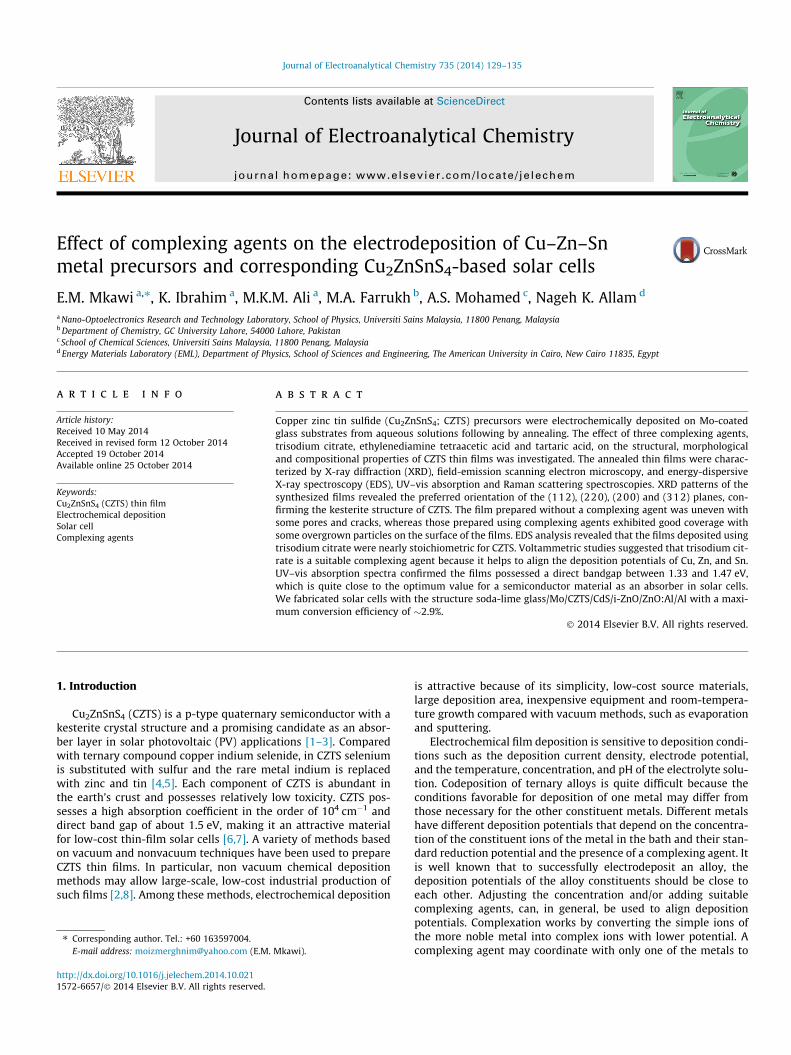
Effect of complexing agents on the electrodeposition of Cu–Zn–Snmetal precursors and corresponding Cu2ZnSnS4-based solar cells
http://dx.doi.org/10.1016/j.jelechem.2014.10.0211572-6657/� 2014 Elsevier B.V. All rights reserved.
⇑ Corresponding author. Tel.: +60 163597004.E-mail address: [email protected] (E.M. Mkawi).
E.M. Mkawi a,⇑, K. Ibrahim a, M.K.M. Ali a, M.A. Farrukh b, A.S. Mohamed c, Nageh K. Allam d
a Nano-Optoelectronics Research and Technology Laboratory, School of Physics, Universiti Sains Malaysia, 11800 Penang, Malaysiab Department of Chemistry, GC University Lahore, 54000 Lahore, Pakistanc School of Chemical Sciences, Universiti Sains Malaysia, 11800 Penang, Malaysiad Energy Materials Laboratory (EML), Department of Physics, School of Sciences and Engineering, The American University in Cairo, New Cairo 11835, Egypt
a r t i c l e i n f o a b s t r a c t
Article history:Received 10 May 2014Received in revised form 12 October 2014Accepted 19 October 2014Available online 25 October 2014
Keywords:Cu2ZnSnS4 (CZTS) thin filmElectrochemical depositionSolar cellComplexing agents
Copper zinc tin sulfide (Cu2ZnSnS4; CZTS) precursors were electrochemically deposited on Mo-coatedglass substrates from aqueous solutions following by annealing. The effect of three complexing agents,trisodium citrate, ethylenediamine tetraacetic acid and tartaric acid, on the structural, morphologicaland compositional properties of CZTS thin films was investigated. The annealed thin films were charac-terized by X-ray diffraction (XRD), field-emission scanning electron microscopy, and energy-dispersiveX-ray spectroscopy (EDS), UV–vis absorption and Raman scattering spectroscopies. XRD patterns of thesynthesized films revealed the preferred orientation of the (112), (220), (200) and (312) planes, con-firming the kesterite structure of CZTS. The film prepared without a complexing agent was uneven withsome pores and cracks, whereas those prepared using complexing agents exhibited good coverage withsome overgrown particles on the surface of the films. EDS analysis revealed that the films deposited usingtrisodium citrate were nearly stoichiometric for CZTS. Voltammetric studies suggested that trisodium cit-rate is a suitable complexing agent because it helps to align the deposition potentials of Cu, Zn, and Sn.UV–vis absorption spectra confirmed the films possessed a direct bandgap between 1.33 and 1.47 eV,which is quite close to the optimum value for a semiconductor material as an absorber in solar cells.We fabricated solar cells with the structure soda-lime glass/Mo/CZTS/CdS/i-ZnO/ZnO:Al/Al with a maxi-mum conversion efficiency of �2.9%.
� 2014 Elsevier B.V. All rights reserved.
1. Introduction
Cu2ZnSnS4 (CZTS) is a p-type quaternary semiconductor with akesterite crystal structure and a promising candidate as an absor-ber layer in solar photovoltaic (PV) applications [1–3]. Comparedwith ternary compound copper indium selenide, in CZTS seleniumis substituted with sulfur and the rare metal indium is replacedwith zinc and tin [4,5]. Each component of CZTS is abundant inthe earth’s crust and possesses relatively low toxicity. CZTS pos-sesses a high absorption coefficient in the order of 104 cm�1 anddirect band gap of about 1.5 eV, making it an attractive materialfor low-cost thin-film solar cells [6,7]. A variety of methods basedon vacuum and nonvacuum techniques have been used to prepareCZTS thin films. In particular, non vacuum chemical depositionmethods may allow large-scale, low-cost industrial production ofsuch films [2,8]. Among these methods, electrochemical deposition
is attractive because of its simplicity, low-cost source materials,large deposition area, inexpensive equipment and room-tempera-ture growth compared with vacuum methods, such as evaporationand sputtering.
Electrochemical film deposition is sensitive to deposition condi-tions such as the deposition current density, electrode potential,and the temperature, concentration, and pH of the electrolyte solu-tion. Codeposition of ternary alloys is quite difficult because theconditions favorable for deposition of one metal may differ fromthose necessary for the other constituent metals. Different metalshave different deposition potentials that depend on the concentra-tion of the constituent ions of the metal in the bath and their stan-dard reduction potential and the presence of a complexing agent. Itis well known that to successfully electrodeposit an alloy, thedeposition potentials of the alloy constituents should be close toeach other. Adjusting the concentration and/or adding suitablecomplexing agents, can, in general, be used to align depositionpotentials. Complexation works by converting the simple ions ofthe more noble metal into complex ions with lower potential. Acomplexing agent may coordinate with only one of the metals to
130 E.M. Mkawi et al. / Journal of Electroanalytical Chemistry 735 (2014) 129–135
shift its electrode potential to the negative side while the secondmetal stays as a simple ion. When a complexing agent forms com-plexes with two types of metal ions, the potentials of both areshifted to more negative values, but the difference between themdecreases. Sometimes, two different complexing agents are addedto coordinate with two different metals. Complexing agents shouldbe nontoxic and noncorrosive. To maximize stability, complexingagents are commonly added to the electrolyte solution in largeramounts than required to achieve stoichiometric composition,leaving some free complexing agent in the electrolyte.
Electrodeposition of CZTS precursors from aqueous solution in asingle step is difficult because of the wide range of reductionpotentials of its constituent metal ions. Ghazali et al. used a com-plexing agent to move the deposition potentials of metal speciescloser together and narrow the potential gap between the electro-lyte elements to obtain a better codeposition environment andproduce stoichiometric thin films of good quality. They realizedthat the free complexing agent in the solution during the electro-deposition process improved the lifetime of the deposition bathas well as the quality of the deposited films, including uniformity,crystallinity and adhesion of the deposited film to the substrate.Addition of ethylenediamine tetraacetic acid (EDTA) preventedthe precipitation of hydroxide. The growth of SnS films using EDTAas a complexing agent has been reported [9]. Pawer et al. [10] usedtrisodium citrate as a complexing agent to fabricate CZTS thin filmsby electrodeposition in an electrolytic bath.
In this work, the effect of different additives with complexingproperties on the electrodeposition of CZTS is investigated. Ourresearch results reveal that the complexing agents in the solutionhave a significant effect on the Cu2ZnSnS4 thin films properties.The influence of these complexing agents on the structural, mor-phological and compositional characteristics of the prepared thinfilms are evaluated and discussed.
2. Experimental details
A Mo/glass substrate with a sheet resistance of ca. 20 X/squarewas used as a cathode for the electrochemical deposition of Cu, Zn,and Sn. Before deposition, the Mo/glass substrate was cleaned bysonication in acetone, followed by immersion in 25 vol% ammoniasolution for 5 min to remove the molybdenum oxide layer (MoOx)on the surface. Electrochemical deposition was performed using aconventional three-electrode system with a Mo-coated soda-limeglass substrate, Pt mesh, and saturated Ag/AgCl as working, coun-ter and reference electrodes, respectively. The working electrodearea was 0.7 cm2. The distance between the working and counterelectrodes was kept constant at about 2 cm. The CV measurementswere carried out from 0 to �1.2 V (vs. Ag/AgCl) without stirring,with a scan rate 10 mV/s at room temperature for 45 min.
CZTS precursors were prepared from solutions containing0.02 M copper (II) sulfate pentahydrate (CuSO4�5H2O), 0.01 M zincsulfate heptahydrate (ZnSO4�7H2O), 0.02 M tin sulfate (SnSO4) andthree complexing agents: tartaric acid (Aldrich, 99%, C4H6O6,50 mM), trisodium citrate (Aldrich, 99%, C6H5Na3O7, 50 mM) andEDTA (Sigma, 99%, C10H16N2O8, 50 mM). The pH of all solutionswas adjusted to 4.75 using HCl and lactic acid. All experimentswere performed at room temperature (18–20 �C). The depositedfilms were annealed using a three-zone tube furnace with a heat-ing rate of 10 �C/min. Sulfur (0.5 g) was evaporated from pelletsat 250 �C from a source placed in the first zone of the furnace.The sulfur vapor was transported along the furnace in a streamof N2 + 5% H2 gas. The samples were heated at 580 �C for 2 h inthe second heating zone.
The solar cell fabrication was completed by depositing a 70 nmCdS layer grown by chemical bath deposition (CBD). The solution
for CBD was prepared by mixing 400 ml of 0.42 mol CH4N2S aque-ous solution, 60 ml of 0.05 mol CdI2 aqueous solution and 110 mlof ammonium hydroxide solution. CBD was carried out by soakingthe SLG/Mo/CZTS in the mixture for 25 min at 70–75 �C. Then itwas dried at 200 �C. Followed by layers of i-ZnO (50 nm)/Al-dopedn-ZnO (500 nm) films were subsequently deposited by a radio fre-quency magnetron sputtering method. An Al (500 nm) grid wasprepared by thermal evaporation.
The structure of the films was studied by X-ray diffraction (XRD)and Raman spectroscopy. XRD patterns were obtained in the 2hrange from 20� to 80� on an X-ray diffractometer (XRD; PANalyticalX’pert PRO MRD PW3040, the Netherlands) with Cu Ka radiation(k = 1.5406 Å) using a step size of 0.02� and step time of 0.3 s. ARaman spectrometer (HR 800 UV, Jobin Yvon, France) was used toobtain Raman spectral measurements. Chemical composition andfilm morphology were determined by energy-dispersive X-rayspectroscopy (EDS) analysis, which was performed using a field-emission scanning electron microscope (FESEM; Nova Nano SEM450, FEI, Japan) equipped with an EDS analyzer. The optical proper-ties of the films were determined using an ultraviolet–visible–nearinfrared spectrophotometer (UV–Vis–NIR; Cary 5000-UV BROP,Agilent Technologies, Australia). Current–voltage measurementswere performed in the dark and under AM1.5 (100 mW cm2)illumination using a power meter (Keithley 2400). Device efficiencywas determined using a solar simulator (SS 1000, Optical RadiationCorporation, France).
3. Results and discussion
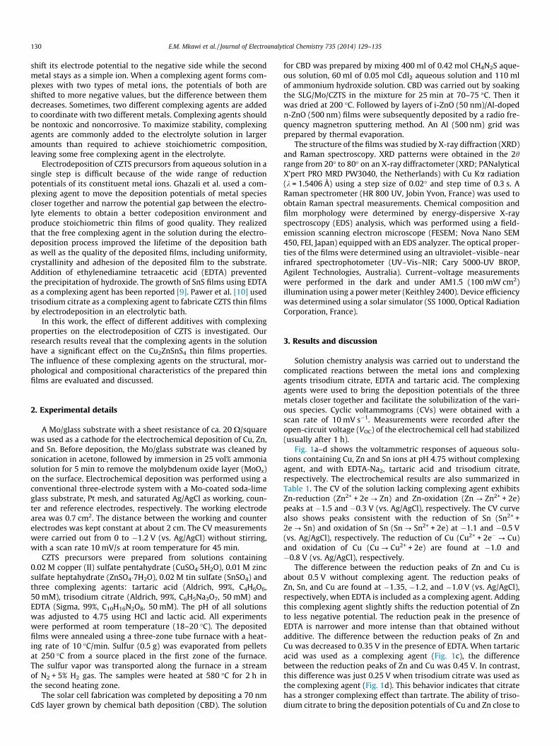
Solution chemistry analysis was carried out to understand thecomplicated reactions between the metal ions and complexingagents trisodium citrate, EDTA and tartaric acid. The complexingagents were used to bring the deposition potentials of the threemetals closer together and facilitate the solubilization of the vari-ous species. Cyclic voltammograms (CVs) were obtained with ascan rate of 10 mV s�1. Measurements were recorded after theopen-circuit voltage (VOC) of the electrochemical cell had stabilized(usually after 1 h).
Fig. 1a–d shows the voltammetric responses of aqueous solu-tions containing Cu, Zn and Sn ions at pH 4.75 without complexingagent, and with EDTA-Na2, tartaric acid and trisodium citrate,respectively. The electrochemical results are also summarized inTable 1. The CV of the solution lacking complexing agent exhibitsZn-reduction (Zn2+ + 2e ? Zn) and Zn-oxidation (Zn ? Zn2+ + 2e)peaks at �1.5 and �0.3 V (vs. Ag/AgCl), respectively. The CV curvealso shows peaks consistent with the reduction of Sn (Sn2+ +2e ? Sn) and oxidation of Sn (Sn ? Sn2+ + 2e) at �1.1 and �0.5 V(vs. Ag/AgCl), respectively. The reduction of Cu (Cu2+ + 2e�? Cu)and oxidation of Cu (Cu ? Cu2+ + 2e) are found at �1.0 and�0.8 V (vs. Ag/AgCl), respectively.
The difference between the reduction peaks of Zn and Cu isabout 0.5 V without complexing agent. The reduction peaks ofZn, Sn, and Cu are found at �1.35, �1.2, and �1.0 V (vs. Ag/AgCl),respectively, when EDTA is included as a complexing agent. Addingthis complexing agent slightly shifts the reduction potential of Znto less negative potential. The reduction peak in the presence ofEDTA is narrower and more intense than that obtained withoutadditive. The difference between the reduction peaks of Zn andCu was decreased to 0.35 V in the presence of EDTA. When tartaricacid was used as a complexing agent (Fig. 1c), the differencebetween the reduction peaks of Zn and Cu was 0.45 V. In contrast,this difference was just 0.25 V when trisodium citrate was used asthe complexing agent (Fig. 1d). This behavior indicates that citratehas a stronger complexing effect than tartrate. The ability of triso-dium citrate to bring the deposition potentials of Cu and Zn close to
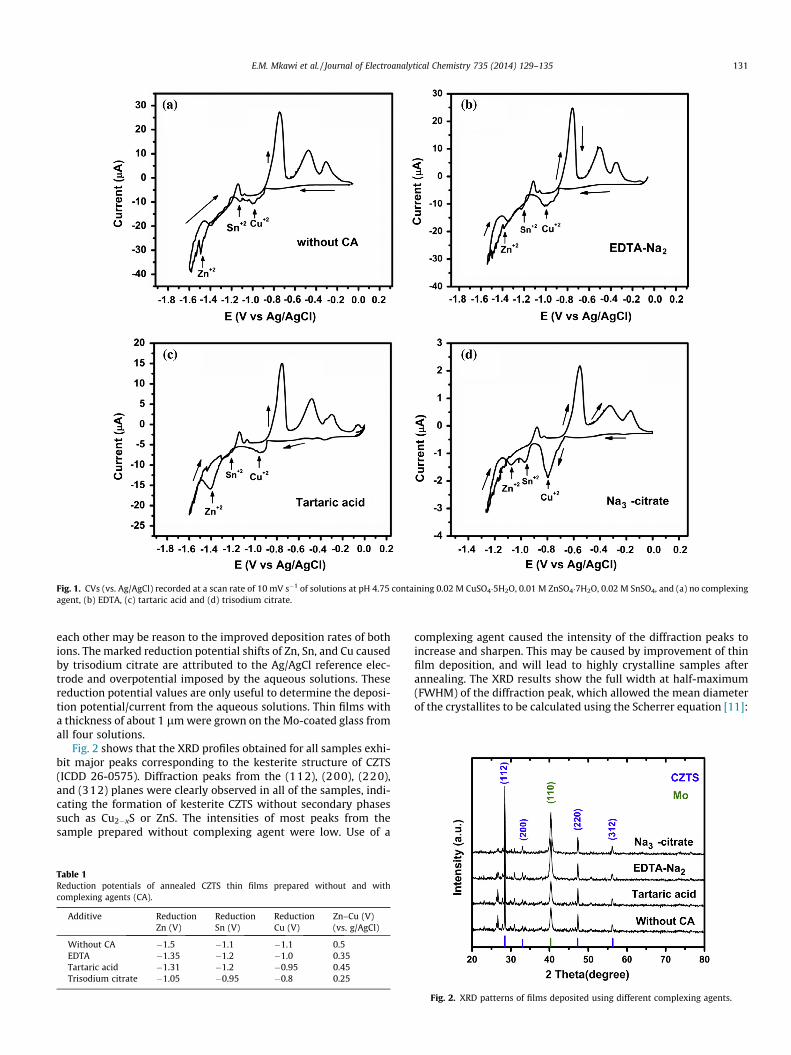
Fig. 1. CVs (vs. Ag/AgCl) recorded at a scan rate of 10 mV s�1 of solutions at pH 4.75 containing 0.02 M CuSO4�5H2O, 0.01 M ZnSO4�7H2O, 0.02 M SnSO4, and (a) no complexingagent, (b) EDTA, (c) tartaric acid and (d) trisodium citrate.
E.M. Mkawi et al. / Journal of Electroanalytical Chemistry 735 (2014) 129–135 131
each other may be reason to the improved deposition rates of bothions. The marked reduction potential shifts of Zn, Sn, and Cu causedby trisodium citrate are attributed to the Ag/AgCl reference elec-trode and overpotential imposed by the aqueous solutions. Thesereduction potential values are only useful to determine the deposi-tion potential/current from the aqueous solutions. Thin films witha thickness of about 1 lm were grown on the Mo-coated glass fromall four solutions.
Fig. 2 shows that the XRD profiles obtained for all samples exhi-bit major peaks corresponding to the kesterite structure of CZTS(ICDD 26-0575). Diffraction peaks from the (112), (200), (220),and (312) planes were clearly observed in all of the samples, indi-cating the formation of kesterite CZTS without secondary phasessuch as Cu2�xS or ZnS. The intensities of most peaks from thesample prepared without complexing agent were low. Use of a
Table 1Reduction potentials of annealed CZTS thin films prepared without and withcomplexing agents (CA).
Additive ReductionZn (V)
ReductionSn (V)
ReductionCu (V)
Zn–Cu (V)(vs. g/AgCl)
Without CA �1.5 �1.1 �1.1 0.5EDTA �1.35 �1.2 �1.0 0.35Tartaric acid �1.31 �1.2 �0.95 0.45Trisodium citrate �1.05 �0.95 �0.8 0.25
complexing agent caused the intensity of the diffraction peaks toincrease and sharpen. This may be caused by improvement of thinfilm deposition, and will lead to highly crystalline samples afterannealing. The XRD results show the full width at half-maximum(FWHM) of the diffraction peak, which allowed the mean diameterof the crystallites to be calculated using the Scherrer equation [11]:
Fig. 2. XRD patterns of films deposited using different complexing agents.
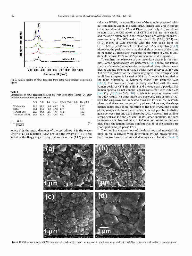
Fig. 3. Raman spectra of films deposited from baths with different complexingagents.
Table 2Composition of films deposited without and with complexing agents (CA) aftersulfurization determined by EDS analysis.
Cu% Zn% Sn% S/m ([Cu]/([Zn] + [Sn]) [Zn]/[Sn]
Without CA 26.8 12.2 14.6 49.7 1.00 0.83EDTA 26.1 13.6 13.2 47.8 0.97 1.03Tartaric acid 25.6 14.3 12.6 47.5 0.95 1.13Trisodium citrate 24.5 14.5 12.1 48.4 0.92 1.19
132 E.M. Mkawi et al. / Journal of Electroanalytical Chemistry 735 (2014) 129–135
D ¼ 0:9kb cos h
ð1Þ
where D is the mean diameter of the crystallites, k is the wave-length of Cu Ka radiation (0.154 nm), B is the FWHM of (112) peakand h is the Bragg angle. Using the width of the (112) peak to
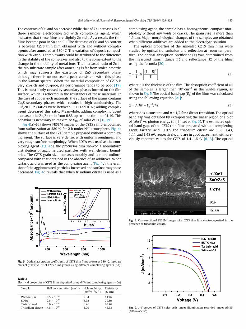
Fig. 4. FESEM surface images of CZTS thin films electrodeposited in (a) the absence of
calculate FWHM, the crystallite sizes of the samples prepared with-out complexing agent, and with EDTA, tartaric acid and trisodiumcitrate are about 6, 12, 12, and 19 nm, respectively. It is importantto note that the XRD patterns of CZTS and ZnS are very similarand the angle differences in the major peaks are within the instru-ment accuracy. The XRD peaks from the (112), (200), (204) and(312) planes of CZTS coincide with the XRD peaks from the(111), (200), (220) and (311) planes of b-ZnS, respectively [12].Moreover, the peak position may shift slightly because of the stressin the material. These facts make the identification of CZTS by XRDdifficult because CZTS and ZnS phases cannot be distinguished.
To confirm the existence of any secondary phases in the sam-ples, Raman spectroscopy was performed. Fig. 3 shows the Ramanspectra of annealed samples electrodeposited using different com-plexing agents. Two main Raman peaks were observed at 287 and338 cm�1 regardless of the complexing agent. The strongest peakin all four samples is located at 338 cm�1, which is identified asthe main vibrational A symmetry mode from kesterite CZTS[10,13]. The two main peaks perfectly matched with the mainRaman peaks of CZTS thins films and monodisperse powder. TheRaman spectra do not contain signals consistent with cubic ZnS[14], Cu2�xS [15] or SnS3 [16], which is in good agreement withthe XRD results. No other peaks are observed. This confirms thatboth the as-grown and annealed films are CZTS in the kesteritephase, and there are no secondary phases. Moreover, the sharp,intense major peak is an indication of the high crystalline qualityof the samples. As mentioned earlier, it is not possible to distin-guish between ZnS and CZTS phases by XRD. However, ZnS exhibitsstrong peaks at 352 and 271 cm�1 in its Raman spectrum, and suchpeaks were not observed here, so ZnS was not present in the sam-ples. Thus, the Raman spectra confirm that all of the samples aregood-quality single-phase CZTS.
The chemical compositions of the deposited and annealed thinfilms on Mo substrates were determined by EDS measurements;the compositions of the annealed samples are listed in Table 2.
complexing agent, and with (b) EDTA, (c) tartaric acid, and (d) trisodium citrate.
E.M. Mkawi et al. / Journal of Electroanalytical Chemistry 735 (2014) 129–135 133
The contents of Cu and Sn decrease while that of Zn increases in allthree samples electrodeposited with complexing agent, whichindicates that these films are slightly Zn rich. As a result, the thinfilms became poor in Sn and Cu. The decrease of Cu and Sn contentis between CZTS thin film obtained with and without complexagents after annealed at 580 �C. The variation of deposit composi-tion with various complexants could be attributed to the differencein the stability of the complexes and also to the some extent to thechange in the mobility of metal ions. The increased ratio of Zn inthe Mo substrate sample after annealing is far from stoichiometric,which may suggests the existence of ZnS secondary phase,although there is no noticeable peak consistent with this phasein the Raman spectra. When the material composition of CZTS isvery Zn-rich and Cu-poor, its performance tends to be poor [17].This is most likely caused by secondary phases formed on the filmsurface, which is reflected in the resistances of these materials. Inthe case of copper-rich materials, the surface of the grains containsCuxS secondary phases, which results in high conductivity. TheCu/(Zn + Sn) ratios were between 1.00 and 0.92; adding complexagent decreased this ratio. Meanwhile, adding complexing agentincreased the Zn/Sn ratio from 0.83 up to a maximum of 1.19. Thisbehavior is necessary to maximize VOC of solar cells [18,19].
Fig 4(a)–(d) shows FESEM images of the CZTS samples obtainedfrom sulfurization at 580 �C for 2 h under N2+ atmosphere. Fig. 4ashows the surface of the CZTS sample prepared without a complex-ing agent. The surface is very dense, with uniform roughness, andvery rough surface morphology. When EDTA was used as the com-plexing agent (Fig. 4b), the precursor film showed a nonuniformdistribution of agglomerated particles with well-defined bound-aries. The CZTS grain size increases notably and is more uniformcompared with that obtained in the absence of an additives. Whentartaric acid was used as the complexing agent (Fig. 4c), the grainsize of the agglomerated particles increased and surface roughnessdecreased. Fig. 4d reveals that when trisodium citrate is used as a
Fig. 5. Optical absorption coefficients of CZTS thin films grown at 580 �C. Inset areplots of (ahm)2 vs. hm of CZTS films grown using different complexing agents (CA).
Table 3Electrical properties of CZTS films deposited using different complexing agents (CA).
Sample Hall concentration (cm�3) Hole mobility(cm2 V�1 S�1)
Resistivity(X cm)
Without CA 9.5 � 1016 9.34 113.6EDTA 2.5 � 1020 5.92 79.59Tartaric acid 3.6 � 1018 6.26 63.46Trisodium citrate 4.5 � 1020 3.79 45.63
complexing agent, the sample has a homogeneous, compact mor-phology without any voids or cracks. The grain size is more than1.5 lm. Major morphological changes of the samples are obtainedwhen different additives are added to the electrolyte solution.
The optical properties of the annealed CZTS thin films werestudied by optical transmission and reflection at room tempera-ture. The optical absorption coefficient (a) was determined fromthe measured transmittance (T) and reflectance (R) of the filmsusing the formula [20]:
a ¼ 1t
lnð1� RÞ2
T
" #ð2Þ
where t is the thickness of the film. The absorption coefficient of allof the samples is larger than 104 cm�1 in the visible region, asshown in Fig. 5. The optical band gap (Eg) of the films was calculatedusing the following equation [21]:
a ¼ Aðhm� EgÞn=hm ð3Þ
where A is a constant, and n = 1/2 for a direct transition. The opticalband gap was obtained by extrapolating the linear region of a plotof (ahm)2 vs. photon energy (hm) (inset of Fig. 5). The estimated opti-cal band gaps of the CZTS thin films prepared without complexingagent, tartaric acid, EDTA and trisodium citrate are 1.38, 1.43,1.44, and 1.48 eV, respectively, and are in good agreement with pre-viously reported values for CZTS of 1.4–1.6 eV [6,13]. The optical
Fig. 6. Cross-sectional FESEM images of a CZTS thin film electrodeposited in thepresence of trisodium citrate.
Fig. 7. J–V curves of CZTS solar cells under illumination recorded under AM15(100 mW cm2).
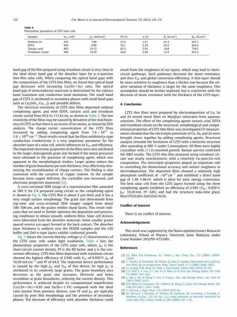
Table 4Photovoltaic parameters of CZTS solar cells.
Samples VOC (mV) JSC (mA/cm2) FF (%) g (%) Rs (X cm2) Rsh (X cm2)
Without CA 435 7.00 53.2 1.61 41.4 425.7EDTA 445 9.00 56.1 2.24 24.3 663.6Tartaric acid 463 10.12 62.3 2.93 16.8 734.5Trisodium citrate 450 10.20 64.0 2.94 12.4 953.4
134 E.M. Mkawi et al. / Journal of Electroanalytical Chemistry 735 (2014) 129–135
band gap of the film prepared using trisodium citrate is very close tothe ideal direct band gap of the absorber layer for p–n-junctionthin-film solar cells. When comparing the optical band gaps withthe compositions of the CZTS thin films, we found that optical bandgap decreases with increasing Cu/(Zn + Sn) ratio. The opticalband gap of semiconductor materials is determined by the valenceband maximum and conduction band minimum. The small bandgap of CZTS is attributed to secondary phases with small band gapssuch as Cu2SnS3, Cu2�xS and possible defects.
The electrical resistivity of CZTS thin films deposited withoutcomplexing agent, and with EDTA, tartaric acid and trisodiumcitrate varied from 45.6 to 113 X cm, as shown in Table 3. The lowresistivity of the films may be caused by deviation of the stoichiom-etry of CZTS so that there is an excess of tin atoms, as shown by EDXanalysis. The charge carrier concentration of the CZTS filmsincreased by adding complexing agent from 7.9 � 1017 to1.6 � 1020 cm�3. These results reveal that the films exhibited p-typeconduction. Conductivity is a very important parameter for theabsorber layer of a solar cell, which influences its VOC and efficiency.The improved electronic properties of the films were also attributedto the larger chalcogenide grain size formed if the metal precursorwere obtained in the presence of complexing agent, which wasapparent in the morphological studies. Larger grains reduce thenumber of grain boundaries per unit thickness, thus effectively min-imizing the recombination of charge carriers. This finding is alsoconsistent with the variation of copper content. As the samplebecame more copper deficient, the crystallite size increased, andelectronic properties improved [22].
A cross-sectional SEM image of a representative film annealedat 580 �C for 2 h prepared using citrate as the complexing agentis shown in Fig. 6. The CZTS film is about 2 lm thick and it has avery rough surface morphology. The grain size determined fromtop-view and cross-sectional SEM images ranged from about100–500 nm, and the grains exhibit sharp facets. This result indi-cates that we need to further optimize the deposition and process-ing conditions to obtain smooth, uniform films. Solar cell deviceswere fabricated from the absorber materials. Some smaller grainsspaced several lm apart formed at the back contact. The absorberlayer thickness is uniform over the FESEM samples and the CdSbuffer and ZnO n-type layers exhibit conformal growth.
Fig. 7 shows the current density–voltage (J–V) characteristics ofthe CZTS solar cells under light irradiation. Table 4 lists thephotovoltaic properties of the CZTS solar cells, where, JSC is theshort-circuit current density, FF is the fill factor, and g is the con-version efficiency. CZTS thin films deposited with trisodium citrateshowed the highest efficiency of 2.94% with VOC of 0.450 V, JSC of10.20 mA cm�2 and FF of 64.0. The improved device performanceis caused by the high JSC and VOC of this device. Its high JSC isattributed to its relatively large grains. The grain boundary areadecreases as the grain size increases. Electrons and holesrecombine at grain boundaries, reducing the current density. Thisperformance is achieved despite its compositional imperfection(Cu/(Zn + Sn) = 0.92 and Zn/Sn = 1.19) compared with the idealratio known from previous devices. Low FF and JSC are typicallycaused by poor film morphology and the presence of secondaryphases. The decrease of efficiency with absorber thickness could
result from the roughness of our layers, which may lead to short-circuit pathways. Such pathways decrease the shunt resistance,and thus VOC and global conversion efficiency. A thin layer shouldbe more sensitive to roughness than a thicker one because the rel-ative variation of thickness is larger for the same roughness. Thisassumption should be further explored, but is consistent with thedecrease of shunt resistance with the thickness of the CZTS layer.
4. Conclusion
CZTS thin films were prepared by electrodeposition of Cu, Snand Zn mixed metal films on Mo/glass substrates from aqueoussolutions. The effect of the complexing agents tartaric acid, EDTAand trisodium citrate on the structural, morphological and compo-sitional properties of CZTS thin films was investigated.CV measure-ments showed that the electrolyte potentials of Cu, Sn, and Zn werebrought closer together by adding complexing agents. Structuralanalysis revealed the formation of CZTS with a kesterite structureafter annealing at 580 �C under S atmosphere. All films were highlycrystalline with (112)-oriented growth. Raman spectra confirmedthe XRD results. The CZTS thin film prepared using trisodium cit-rate was nearly stoichiometric with a relatively Cu-poor/Zn-richcomposition. The electrolyte properties played an important rolein controlling the dimensional accuracy and surface roughness inelectrodeposition. The deposited films showed a relatively highabsorption coefficient of �104 cm�1 and exhibited a direct bandgap of 1.38–1.48 eV, which is ideal for solar energy conversion.The best solar cell from the CZTS layers formed using the threecomplexing agents exhibited an efficiency of 2.94% (VOC: 0.450 V,JSC: 10.20 mA, FF: 64%) and had the structure soda-lime glass/Mo/CZTS/CdS/i-ZnO/ZnO:Al/Al.
Conflict of interest
There is no conflict of interest.
Acknowledgement
This work was supported by the Nano-optoelectronics ResearchLaboratory, School of Physics, Universiti Sains Malaysia underGrant Number 203/PSF-6721001.
References
[1] S.C. Riha, B.A. Parkinson, A.L. Prieto, J. Am. Chem. Soc. 131 (2009) 12054–12055.
[2] T. Tanaka, D. Kawasaki, M. Nishio, Q. Guo, H. Ogawa, Fabrication of Cu2ZnSnS4
thin films by co-evaporation, Phys. Status Solidi (c) 3 (2006) 2844–2847.[3] J.J. Scragg, D.M. Berg, P.J. Dale, J. Electroanal. Chem. 646 (2010) 52–59.[4] J.-S. Seol, S.-Y. Lee, J.-C. Lee, H.-D. Nam, K.-H. Kim, Sol. Energy Mater. Sol. Cells
75 (2003) 155–162.[5] L. Sun, J. He, H. Kong, F. Yue, P. Yang, J. Chu, Sol. Energy Mater. Sol. Cells 95
(2011) 2907–2913.[6] D.B. Mitzi, O. Gunawan, T.K. Todorov, K. Wang, S. Guha, Sol. Energy Mater. Sol.
Cells 95 (2011) 1421–1436.[7] C. Persson, J. Appl. Phys. 107 (2010) 053710.[8] M. Altosaar, J. Raudoja, K. Timmo, M. Danilson, M. Grossberg, J. Krustok, E.
Mellikov, Cu2Zn1�xCdx Sn (Se1�ySy)4 solid solutions as absorber materials forsolar cells, Phys. Status Solidi (a) 205 (2008) 167–170.

E.M. Mkawi et al. / Journal of Electroanalytical Chemistry 735 (2014) 129–135 135
[9] A. Ghazali, Z. Zainal, M. Zobir Hussein, A. Kassim, Cathodic electrodeposition ofSnS in the presence of EDTA in aqueous media, Sol. Energy Mater. Sol. Cells 55(1998) 237–249.
[10] B. Pawar, S. Pawar, S. Shin, D. Choi, C. Park, S. Kolekar, J. Kim, Appl. Surf. Sci.257 (2010) 1786–1791.
[11] E. Johnson, R. Willardson, A. Beer, Semiconductors and semimetals, Opt. Prop.III–V Compd. 3 (1967) 153.
[12] H. Katagiri, K. Jimbo, W.S. Maw, K. Oishi, M. Yamazaki, H. Araki, A. Takeuchi,Thin Solid Films 517 (2009) 2455–2460.
[13] P. Fernandes, P. Salomé, A. Da Cunha, Thin Solid Films 517 (2009) 2519–2523.[14] J. Serrano, A. Cantarero, M. Cardona, N. Garro, R. Lauck, R. Tallman, T. Ritter, B.
Weinstein, Phys. Rev. B 69 (2004) 014301.
[15] C.G. Munce, G.K. Parker, S.A. Holt, G.A. Hope, Coll. Surf. A: Physicochem. Eng.Asp. 295 (2007) 152–158.
[16] I. Parkin, L. Price, T. Hibbert, K. Molloy, J. Mater. Chem. 11 (2001) 1486–1490.[17] S. Chen, J.-H. Yang, X. Gong, A. Walsh, S.-H. Wei, Phys. Rev. B 81 (2010) 245204.[18] H. Katagiri, Thin Solid Films 480 (2005) 426–432.[19] H. Katagiri, K. Jimbo, S. Yamada, T. Kamimura, W.S. Maw, T. Fukano, T. Ito, T.
Motohiro, Appl. Phys. Expr. 1 (2008) 041201.[20] J.I. Pankove, Semiconductors & Semimetals V21B, Academic Press, 1984.[21] C. Chan, H. Lam, C. Surya, Sol. Energy Mater. Sol. Cells 94 (2010) 207–211.[22] T. Prabhakar, N. Jampana, Sol. Energy Mater. Sol. Cells 95 (2011) 1001–1004.
Copyright © 2022 FDOKUMEN


![Complexes with lignin model compound vanillic acid. Two different carboxylate ligands in the same dinuclear tetracarboxylate complex [Cu2(C8H7O4)2(O2CCH3)2(CH3OH)2]](https://static.fdokumen.com/doc/165x107/634161588e4a224f800682ce/complexes-with-lignin-model-compound-vanillic-acid-two-different-carboxylate-ligands.jpg)