Morpho-structural properties of CeO2 and (CeO2-CaO, CeO2-ZnO) Binary Nanostructured Oxides Prepared...
16
[Bazzi, 3(9): September, 2014] ISSN: 2277-9655 Scientific Journal Impact Factor: 3.449 (ISRA), Impact Factor: 1.852 http: // www.ijesrt.com (C)International Journal of Engineering Sciences & Research Technology [173] IJESRT INTERNATIONAL JOURNAL OF ENGINEERING SCIENCES & RESEARCH TECHNOLOGY Morpho-structural properties of CeO2 and (CeO2-CaO, CeO2-ZnO) Binary Nanostructured Oxides Prepared by the Electrodeposition Method M. El Hajji 1 , A. Hallaoui 1 , L. Bazzi 1 *, O. Jbara 2 , A. Benlhachemi 1 , A. Tara 2 , B.Bakiz 1 1 Material and Environment Laboratory (LME), Faculty of Sciences, Agadir, Morocco. 2 Engineering and Materials Science Laboratory (LISM), UFR Sciences, University of Reims, France. [email protected] Abstract Ceria thin films (CeO 2 ) were prepared by electrochemical cathodic deposition process. Different types of substrates were used such as aluminum, titanium and stainless steel. As it is possible to deposit separately pure ceria (CeO 2 ), pure calcium oxide (CaO) and pure Zinc oxide (ZnO), CeO 2 -CaO and CeO 2 -ZnO binary oxides thin films were successfully obtained in one electrochemical condition set. By varying the current density, deposition time and electrolyte concentration, the amount of the electrodeposited material could be controlled. The deposits were studied by X-ray diffraction (XRD) and scanning electron microscopy « SEM » coupled to energy dispersive spectrometry « EDS » Keywords: Electrochemical Cathodic Deposition, CeO 2 , CeO 2 -CaO, CeO 2 -ZnO, X-ray diffraction, SEM, EDS. Introduction Nowadays, nanostructured metal oxides are subject of a tremendous attention because of their electronic and optical properties as well as their potential applications; especially in sensors, catalysts, for protection against corrosion, and in electrochemical degradation of waste waters [1-7]. Among the most active rare-earth oxides, ceria has attracted much interest owing to its unique properties including high mechanical strength, oxygen ion conductivity, and oxygen storage capacity. Cerium oxide (CeO2) has been employed as catalyst [8], catalyst support [9,10], for the development of biosensors [11], and in solid fuel electrolyte industries [12]. Ceria thin films have been prepared with different processes such as ion beam deposition [13-16], chemical vapor deposition [17-21], sputtering [22,23], pulsed laser deposition/ablation [24,25], and sol –gel process [26,27]. The electrochemical deposition process has been claimed to become an important method on the processing of this oxide because of the low cost of equipment, also, the films can be obtained on a vast variety of substrates [28-31]. By means of electrodeposition, the morphology and size of metal-oxide crystals are easily controlled by variation in the potential, current density, and concentration of the reactant. The aim of this study is therefore to elaborate and to characterize the films of pure cerium oxide and nanocomposite cerium binary oxides CeO2-CaO and CeO2-ZnO electrodeposited from precursor using a classic three-electrode cell. The correlation between the electrochemical deposition and the characteristics of the films developed on three kinds of substrates was established through chronopotentiometry experiments, X-ray diffraction « XRD » and scanning electron microscopy « SEM » coupled to energy dispersive spectrometry « EDS ». Materials and methods All chemicals used to prepare the thin films, were purchased from Sigma Aldrich. The electrochemical cell used for electrodeposition had been described elsewhere [32]. Stainless steel (SS), aluminum (Al) and titanium (Ti) substrates were used as working electrode. Prior to the deposition, substrates were polished mechanically using a mechanical polishing machine on a paper of polishing SiC 600, 800 and SiC 1200 for the completion. Then, the substrates were washed thoroughly with distilled water, rinsed with acetone, and cleaned with ethanol. Finally, they were dried with pulsed hot air immediately before the deposition. XRD analysis was carried out using a BURKER SIEMENS D5000, with Cu Kα1 source (λ = 1.5406 Å) at a glancing angle of 0.5°. To study the surface morphology of obtained films, SEM observation was carried out using Philips XL 30 ESEM-Field-Emission Gun.
Transcript of Morpho-structural properties of CeO2 and (CeO2-CaO, CeO2-ZnO) Binary Nanostructured Oxides Prepared...

[Bazzi, 3(9): September, 2014] ISSN: 2277-9655
Scientific Journal Impact Factor: 3.449
(ISRA), Impact Factor: 1.852
http: // www.ijesrt.com (C)International Journal of Engineering Sciences & Research Technology
[173]
IJESRT INTERNATIONAL JOURNAL OF ENGINEERING SCIENCES & RESEARCH
TECHNOLOGY
Morpho-structural properties of CeO2 and (CeO2-CaO, CeO2-ZnO) Binary
Nanostructured Oxides Prepared by the Electrodeposition Method M. El Hajji1, A. Hallaoui1, L. Bazzi1*, O. Jbara2, A. Benlhachemi1, A. Tara2, B.Bakiz1
1 Material and Environment Laboratory (LME), Faculty of Sciences, Agadir, Morocco. 2 Engineering and Materials Science Laboratory (LISM), UFR Sciences, University of Reims, France.
Abstract Ceria thin films (CeO2) were prepared by electrochemical cathodic deposition process. Different types of
substrates were used such as aluminum, titanium and stainless steel. As it is possible to deposit separately pure ceria
(CeO2), pure calcium oxide (CaO) and pure Zinc oxide (ZnO), CeO2-CaO and CeO2-ZnO binary oxides thin films
were successfully obtained in one electrochemical condition set. By varying the current density, deposition time and
electrolyte concentration, the amount of the electrodeposited material could be controlled. The deposits were studied
by X-ray diffraction (XRD) and scanning electron microscopy « SEM » coupled to energy dispersive spectrometry
« EDS »
Keywords: Electrochemical Cathodic Deposition, CeO2, CeO2-CaO, CeO2-ZnO, X-ray diffraction, SEM, EDS.
Introduction Nowadays, nanostructured metal oxides are
subject of a tremendous attention because of their
electronic and optical properties as well as their
potential applications; especially in sensors, catalysts,
for protection against corrosion, and in
electrochemical degradation of waste waters [1-7].
Among the most active rare-earth oxides, ceria has
attracted much interest owing to its unique properties
including high mechanical strength, oxygen ion
conductivity, and oxygen storage capacity. Cerium
oxide (CeO2) has been employed as catalyst [8],
catalyst support [9,10], for the development of
biosensors [11], and in solid fuel electrolyte
industries [12]. Ceria thin films have been prepared
with different processes such as ion beam deposition
[13-16], chemical vapor deposition [17-21],
sputtering [22,23], pulsed laser deposition/ablation
[24,25], and sol–gel process [26,27]. The
electrochemical deposition process has been claimed
to become an important method on the processing of
this oxide because of the low cost of equipment, also,
the films can be obtained on a vast variety of
substrates [28-31]. By means of electrodeposition,
the morphology and size of metal-oxide crystals are
easily controlled by variation in the potential, current
density, and concentration of the reactant.
The aim of this study is therefore to elaborate and to
characterize the films of pure cerium oxide and
nanocomposite cerium binary oxides CeO2-CaO and
CeO2-ZnO electrodeposited from precursor using a
classic three-electrode cell. The correlation between
the electrochemical deposition and the characteristics
of the films developed on three kinds of substrates
was established through chronopotentiometry
experiments, X-ray diffraction « XRD » and scanning
electron microscopy « SEM » coupled to energy
dispersive spectrometry « EDS ».
Materials and methods All chemicals used to prepare the thin films,
were purchased from Sigma Aldrich. The
electrochemical cell used for electrodeposition had
been described elsewhere [32]. Stainless steel (SS),
aluminum (Al) and titanium (Ti) substrates were used
as working electrode. Prior to the deposition,
substrates were polished mechanically using a
mechanical polishing machine on a paper of
polishing SiC 600, 800 and SiC 1200 for the
completion. Then, the substrates were washed
thoroughly with distilled water, rinsed with acetone,
and cleaned with ethanol. Finally, they were dried
with pulsed hot air immediately before the
deposition. XRD analysis was carried out using a
BURKER SIEMENS D5000, with Cu Kα1 source (λ
= 1.5406 Å) at a glancing angle of 0.5°. To study the
surface morphology of obtained films, SEM
observation was carried out using Philips XL 30
ESEM-Field-Emission Gun.
[Bazzi, 3(9): September, 2014] ISSN: 2277-9655
Scientific Journal Impact Factor: 3.449
(ISRA), Impact Factor: 1.852
http: // www.ijesrt.com (C)International Journal of Engineering Sciences & Research Technology
[174]
Electrodeposition of cerium oxide
Electrochemical deposition experiments were
performed from aqueous solution of cerium nitrate
0.1M «Ce(NO3)3,6 H2O » 99%, in galvanostatic
regime without stirring and at room temperature. The
cathodic deposition at current densities ranging from
1 to 3 mA.cm-2 was investigated. The pH was about
3.6. After electrodeposition, the samples were rinsed
in ethanol and placed in a desiccator before any
further subsequent analysis. Deposit weights were
obtained by weighing the substrates before and after
deposition experiments.
Electrodeposition of CeO2-CaO
CeO2-CaO was electrodeposited using the following
chemical products: 0.05 M cerium nitrate;
Ce(NO3)3•6H2O; like cerium precursor, 0.0125 M
calcium nitrate; Ca(NO3)2; like calcium precursor,
and 0.1 M potassium nitrate « KNO3 » like
electrolyte support. The electrodeposition was
realized using a classical three-electrode
experimental set-up [32], with the stainless steel
sample being the cathode. The pH of the electrolytic
bath was 4.6, and the used cathodic current density
was 3.5mA/cm2.
Electrodeposition of CeO2-ZnO
In this part only stainless steel substrate was used as
working electrode. To prepare the thin films of CeO2-
ZnO nanocomposite, the following chemical products
used were: 0.025M zinc nitrate; Zn(NO3)2•6H2O; like
zinc precursor, 0.1M cerium nitrate;
Ce(NO3)3 ,6H2O; like cerium precursor, and 0.5M
potassium nitrate « KNO3 » like electrolyte support.
The deposition experiments were carried out in the
galvanostatic mode without stirring the solution, at
room temperature, and the used current density was
2.5mA/cm2.
Results and discussion Electrochemical deposition of Ceria:
Electrochemical mechanism:
The electrochemical mechanism of deposition was
largely discussed in the literature [33,34]. Two steps
must be distinguished. The first step corresponds to
the cathodic generation of ions hydroxyl OH- by the
reduction of O2, H2O or NO3-.
O2 + 2H2O + 4e-<====> 4OH- (1)
2H2O + 2e- <====> H2 (g) + 2OH- (2)
NO3- + H2O + 2e- <====> NO2
- + 2OH- (3)
The second step corresponds to the reaction of
precipitation of cerium hydroxide. The formation of
hydroxyl ions leads to the local increase of pH on the
surface followed by the formation of a precipitate
Ce(OH)3 [35].
Ce3+ + 3OH- Ce(OH)3 (4)
Then, cerium oxide thin film is formed from the
oxidation of Ce(OH)3 (Eq.(5)).
Ce(OH)3 <====>CeO2 + H3O+ + e- (5)
Ceria electrochemical mechanism is really
complicated. Li and Thompson [36] suggested that
the deposition of the film is preceded by nucleation
and a process of growth. For more cathodic current
densities, a quick and monotonous decrease of
potential is observed in the first few seconds
followed by a stabilization of the potential. Such
stabilization appears sooner by increasing the applied
current density. However, at less current density
(lower than or 0.5mAcm−2), the electrodeposition
passes by several stages before the potential stabilizes
and the obtained film is not homogenous and it
contains several cracks [37]. Figure. 1 gives the
variation of potential versus time during deposition.
In order to obtain homogeneous and less to free crack
thin film, the applied current density was about
3mA/cm2. A continuous variation of potential with
time is indicative of a single reaction, whereas
sudden changes are indicative of a change in the
dominant reaction taking place at the electrode.
The chronopotentiometric curve related to CeO2 film
exhibit a particular shape.
[Bazzi, 3(9): September, 2014] ISSN: 2277-9655
Scientific Journal Impact Factor: 3.449
(ISRA), Impact Factor: 1.852
http: // www.ijesrt.com (C)International Journal of Engineering Sciences & Research Technology
[175]
Actually, upon the application of the current density,
the cathodic potential increases, as the formation of
ceria hydroxide occurs. Over the first 200 s, the
potential decreases and reaches the value of about
1520 mV. The second part of the process was
characterized by constant potential. This part of
process was assigned to the homogenous crystal
growths. In this case, only reaction responsible for
electrogeneration of OH- is related to the hydrogen
evolution reactions. In the initial stage of deposition,
the nucleation and the growth of nuclei compete with
each other. In the case of high current density “more
than 2mA/cm2”, the generation reaction rate is high,
and the rate of nucleation exceeds that of growth of
nuclei. The first period (t < 2000 s) is attributed to the
formation of a deposit of fine particle size that fully
covers the surface. Therefore, the potential stabilizes
rapidly. It can be related to the stacking of new
layers.
The deposit weight was determined according to
Faraday’s law. Electrolytic deposition experiments
revealed the formation of cathodic deposits from
cerium nitrate solutions. Figure.2 shows the deposit
weight as a function of deposition time for 0.1 M
Ce(NO3)3,6 H2O solution. Lower deposit weights
were obtained at lower deposition time. It should be
noted that in low concentration of electrolytes the
rate of hydrolysis reactions depends on the rate of
diffusion of the reacting species, detracting from the
deposition process efficiency. Globally, nearly linear
dependence was observed.
Figure.1. Evolution of potential with deposition
time in 0.1M Ce(III) nitrate solutions, 3 mA.cm-2
and at room temperature.
Figure. 2. Deposit weight vs. deposition time for
deposits obtained from 0.1 M cerium nitrate
solution at a current density of 3mA/cm2.
Characterization of the deposits
The XRD studies were carried out on CeO2 in order
to determine phase and crystallographic analysis. All
obtained XRD patterns were analyzed using the
X'Pert HighScore software. Typical X-ray
diffractogram of electrodeposited CeO2 onto
aluminum (Al) substrate is shown in figure 3.
The peaks located at 2θ = 28.31°, 32.96°, 47.56° and
56.31° could be related to the (111), (200), (220) and
(311) reflections of the cerium oxide species,
respectively. They are generally less intense
compared to Al peaks. According to JCPDS 43-1002,
the registered peaks clearly confirm that the cubic
fluorite CeO2 phase is the compound diffracting from
the thin film. As observed from the figure 3 that,
XRD peak (111) is the more dominant against others.
To study the effect of changing the substrate, we had
electrodeposited CeO2 onto SS and Ti substrates,
respectively. The results are shown in figure 4 and 5.

[Bazzi, 3(9): September, 2014] ISSN: 2277-9655
Scientific Journal Impact Factor: 3.449
(ISRA), Impact Factor: 1.852
http: // www.ijesrt.com (C)International Journal of Engineering Sciences & Research Technology
[176]
From figure.4, The XRD pattern shows the material
to be polycrystalline and a strongest peak
corresponding to the (111) plane appeared. Contrary
to figure.3, the peaks related to SS substrate are less
intense.
In figure.5, the XRD patterns of electrodeposited
CeO2 onto Ti substrate are displayed. Generally,
diffraction lines of both films can be indexed as CeO2
structure. Diffraction peaks match well with the
peaks of cubic fluorite CeO2 crystal structure. The
broadening of the diffraction peaks indicates the
formation of nanocrystals. As observed, XRD peak
(111) located at 2θ = 28.5° is the dominant one in all
patterns. Lower intensity peaks, also detected in the
patterns at the following 2θ values of 33°, 47.6°,
56.3°, are assigned to (200), (220) and (311)
crystallographic planes, respectively. With the
appearance of the new peaks corresponding to the
(222) “Figure.4” and (331) “Figure 5” planes,
matching to ceria.
Table.1. shows the calculated average size of the
crystallites of electrodeposited CeO2 onto SS , Al and
Ti substrates. The grain sizes estimated from the X-
ray diffraction peak width, using Scherrer’s formula
[38] were between 17 and 23 nm. This result
confirms the good crystallinity of the samples and the
nanometric size of crystallites.
Figure. 3. XRD patterns of nanostructured CeO2 films electrodeposited on Al substrate
Figure. 4. XRD patterns of nanostructured CeO2 films electrodeposited on SS substrate

[Bazzi, 3(9): September, 2014] ISSN: 2277-9655
Scientific Journal Impact Factor: 3.449
(ISRA), Impact Factor: 1.852
http: // www.ijesrt.com (C)International Journal of Engineering Sciences & Research Technology
[177]
Figure. 5. XRD patterns of nanostructured CeO2 films electrodeposited on Ti substrate
Table.1. : Average grain size of CeO2 calculated by the Scherrer’s equation
Substrate Crystallites size (nm)
Ti 21.7
SS 23.3
Al 17.5
SEM observation was used to investigate the surface
morphology. Figure.6 illustrates the appearance of
the electrodeposited CeO2 onto Al substrate showing
homogeneous and void-free surface. It can be seen
that the films fully covers the surface of the substrate.
Figure.7 shows the SEM images of the CeO2 deposit
obtained using different magnification. Generally,
the products were observed as nanostructures with
diameters of a few tens of nanometers on the
substrate. The length of nanostructures is up to a few
micrometers. The film exhibits some cracks
(figure.7a). Figure.7b allows us to view that the
layers obtained had a specific morphology. The
enlarging of a grain makes it possible to visualize the
layer covered with small fine grains like the hair shapes (Figure.7c). SEM provides information not
only on morphology, the distribution and the size of
the grains or the agglomerates, but also on the local
chemical composition when it is coupled with EDS
X-Ray spectrometer. Figure.8 shows the results
obtained by EDS X-Ray analysis of pure ceria. The
EDS analysis confirms the presence of oxygen, and
cerium elements in the deposit. The weight elements
percentage was close of the nominal composition.
Figure.8. EDS spectrum related to the deposit of the
pure cerium oxide. The SEM image (A) indicates the
zone where the spectrum is acquired. The inserted
table indicates the weight percents of ceria elements.

[Bazzi, 3(9): September, 2014] ISSN: 2277-9655
Scientific Journal Impact Factor: 3.449
(ISRA), Impact Factor: 1.852
http: // www.ijesrt.com (C)International Journal of Engineering Sciences & Research Technology
[178]
Figure.6. SEM micrograph of electrodeposited CeO2 on Al substrate
Figure.7. Typical SEM images of thin films grown on Al substrate at different magnifications
a b

[Bazzi, 3(9): September, 2014] ISSN: 2277-9655
Scientific Journal Impact Factor: 3.449
(ISRA), Impact Factor: 1.852
http: // www.ijesrt.com (C)International Journal of Engineering Sciences & Research Technology
[179]
Figure.8. EDS spectrum related to the deposit of the pure cerium oxide.
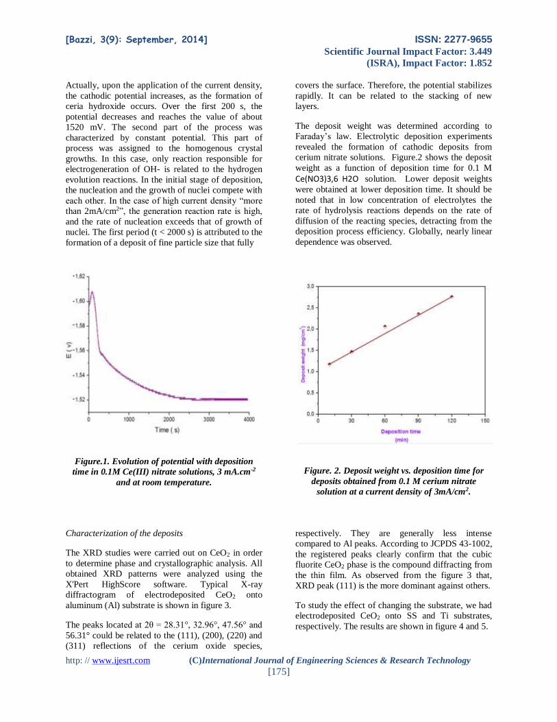
As we had already noted that, the cathodic deposition
of ceria was made onto three different substrates such titanium, aluminum, and stainless steel. It is
important to note that deposits of the similar
microstructure were obtained on these various metal
surfaces.
Figure.9. illustrates the SEM micrographics of the
electrodeposited pure CeO2 thin film. Although both
films fully cover the substrate, it is easy to observe
that the thin film of ceria electrodeposited on SS and
Ti exhibit the same morphology on Al (figure.7).
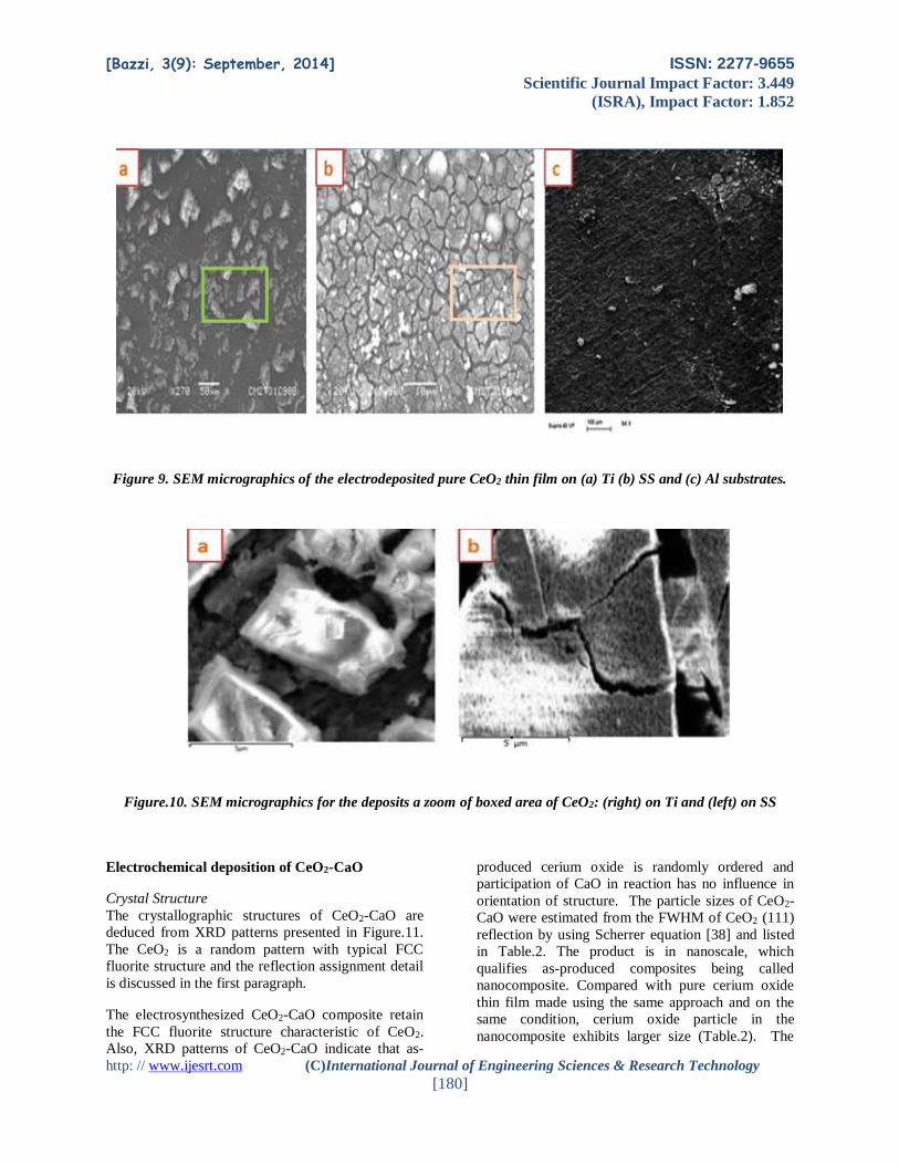
This result is confirmed in Figure.10 (a and b). It
represents the magnifications of two zones: (left) the
enlargement of an area of CeO2 deposited on SS, and
on Ti (right).
Globally, electrodeposited ceria thin films have a
smooth surface and exhibit a close morphology
independent on the substrate used. The Al substrate
gives rise to dense ceria thin films-based on hair
shaped nanoparticles. On the other hand, ceria
exhibits a close structure when grown on the Ti and
SS substrates. A magnified image shows that it is
composed of even smaller, tiny, interconnected
nanoparticles like needle. From the SEM graph some
cracks marked significantly the structure. Especially,
on stainless steel and titanium substrate, extensive
cracking can be seen on the film surface. These
cracks are associated with either the formation of gas
bubbles during the process on the substrate surface,
to the dehydration process itself, to a large mismatch
between the substrate and film, or drying process
[39]. EDS X-Ray analysis confirms the presence of
oxygen, and cerium elements in the deposit. Also, the
XRD patterns confirm that the cubic fluorite CeO2
phase is the major compound diffracting from the
deposits. No diffraction line associated with Ce (III)
hydroxide is present. Likewise, no broad spot
appears. Normally, this spot is coupled to the
carbonation of the ceria films which can be
responsible for the formation of the green rust. It is
associated to the corrosion, especially, on the
stainless steel substrate. These results have been
confirmed by SEM/EDS analysis.
A
[Bazzi, 3(9): September, 2014] ISSN: 2277-9655
Scientific Journal Impact Factor: 3.449
(ISRA), Impact Factor: 1.852
http: // www.ijesrt.com (C)International Journal of Engineering Sciences & Research Technology
[180]
Figure 9. SEM micrographics of the electrodeposited pure CeO2 thin film on (a) Ti (b) SS and (c) Al substrates.
Figure.10. SEM micrographics for the deposits a zoom of boxed area of CeO2: (right) on Ti and (left) on SS
Electrochemical deposition of CeO2-CaO
Crystal Structure
The crystallographic structures of CeO2-CaO are
deduced from XRD patterns presented in Figure.11.
The CeO2 is a random pattern with typical FCC
fluorite structure and the reflection assignment detail
is discussed in the first paragraph.
The electrosynthesized CeO2-CaO composite retain
the FCC fluorite structure characteristic of CeO2.
Also, XRD patterns of CeO2-CaO indicate that as-
produced cerium oxide is randomly ordered and
participation of CaO in reaction has no influence in
orientation of structure. The particle sizes of CeO2-
CaO were estimated from the FWHM of CeO2 (111)
reflection by using Scherrer equation [38] and listed
in Table.2. The product is in nanoscale, which
qualifies as-produced composites being called
nanocomposite. Compared with pure cerium oxide
thin film made using the same approach and on the
same condition, cerium oxide particle in the
nanocomposite exhibits larger size (Table.2). The

[Bazzi, 3(9): September, 2014] ISSN: 2277-9655
Scientific Journal Impact Factor: 3.449
(ISRA), Impact Factor: 1.852
http: // www.ijesrt.com (C)International Journal of Engineering Sciences & Research Technology
[181]
peaks of cerium and calcium oxides are confused at
2and no diffraction line associated with
hydroxide is present.
Figure.11. XRD patterns for CeO2-CaO nanocomposite oxide
Table.2. CeO2 Particle size vs. content of CaO in nanocomposite
Samples SS/Ceria
(Fig.4)
SS/CeO2-CaO
(Fig.11)
Reflection 28.31 28.59
Particle size (nm) 39.4 74.2

[Bazzi, 3(9): September, 2014] ISSN: 2277-9655
Scientific Journal Impact Factor: 3.449
(ISRA), Impact Factor: 1.852
http: // www.ijesrt.com (C)International Journal of Engineering Sciences & Research Technology
[182]
Surface Morphologies of Films
The morphologies of as-formed nanocomposite
oxides were examined using scanning electron
microscopy “SEM “. Fig.12 shows the appearance of
the electrodeposited CeO2-CaO onto stainless steel
substrate showing homogeneous and cracking
surface. Figure.13 illustrates the selected SEM
pictures of the CeO2-CaO composite films obtained
using different magnification. Since, CaO oxide is
more readily to interact with the cerium oxide system
in an aqueous reaction environment, which can be
verified in the morphology of the films. The CeO2-
CaO nanocomposite, at a certain content of calcium,
gives a homogenous surface with the calcium
incorporated with the cerium oxide surface. As
predicted, the galvanostatic deposition mode with
applied current –3.5mA/cm2 at 30oC (room
temperature) leads to more CeO2 (111) preferred
structure (figure 11). The enlarging of a zone (figure
13) makes it possible to visualize a cluster of grains
of micrometric size. The usual form of the cerium
oxide is observed. However, on the film surface some
cracks appears but they are less significant compared
with the ceria (figure.7a). As discussed in the
literature [40], these cracks are associated with either
the formation of gas bubbles, to the dehydratation
process itself or from the shearing stress between the
substrate and the deposit. In this case, the second
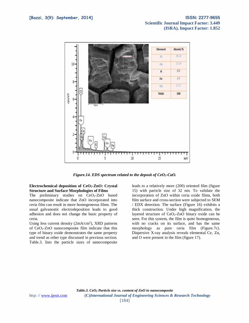
proposal remains most probable. EDX on cross-
section and surface of CeO2-CaO nanocomposite
films reveals presence of elemental Ce, Ca, and O in
the nanocomposite films (figure 14). Among those,
Fe and K are attributed to stainless steel substrate.
Figure.12. SEM micrograph of electrodeposited CeO2-CaO
[Bazzi, 3(9): September, 2014] ISSN: 2277-9655
Scientific Journal Impact Factor: 3.449
(ISRA), Impact Factor: 1.852
http: // www.ijesrt.com (C)International Journal of Engineering Sciences & Research Technology
[183]
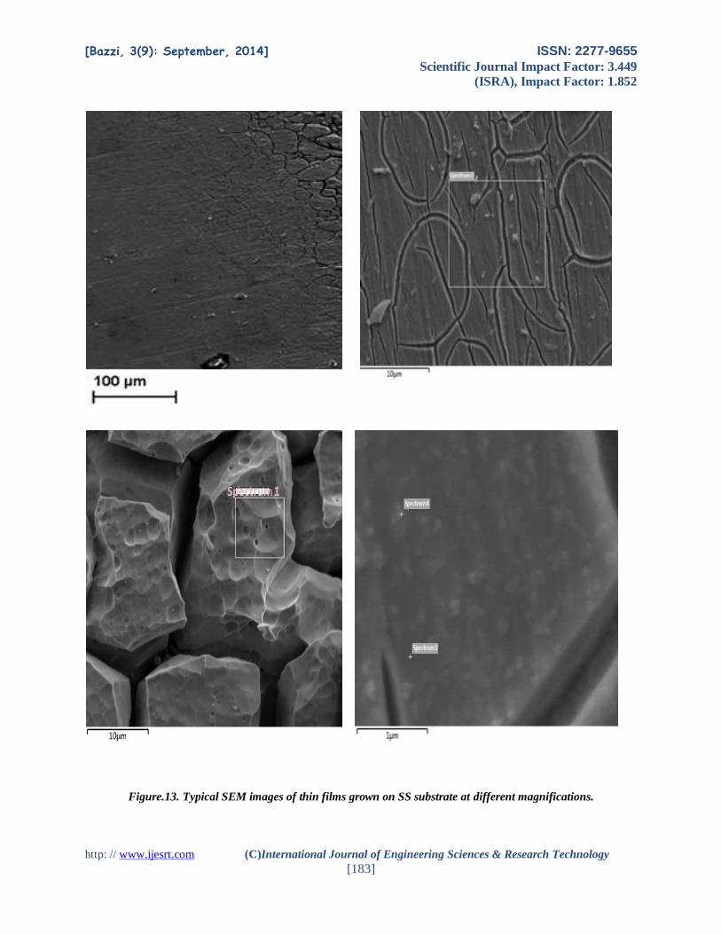
Figure.13. Typical SEM images of thin films grown on SS substrate at different magnifications.
[Bazzi, 3(9): September, 2014] ISSN: 2277-9655
Scientific Journal Impact Factor: 3.449
(ISRA), Impact Factor: 1.852
http: // www.ijesrt.com (C)International Journal of Engineering Sciences & Research Technology
[184]
Figure.14. EDS spectrum related to the deposit of CeO2-CaO.
Electrochemical deposition of CeO2-ZnO: Crystal
Structure and Surface Morphologies of Films
The preliminary studies on CeO2-ZnO based
nanocomposite indicate that ZnO incorporated into
ceria film can result in more homogeneous films. The
usual galvanostic electrodeposition leads to good
adhesion and does not change the basic property of
ceria.
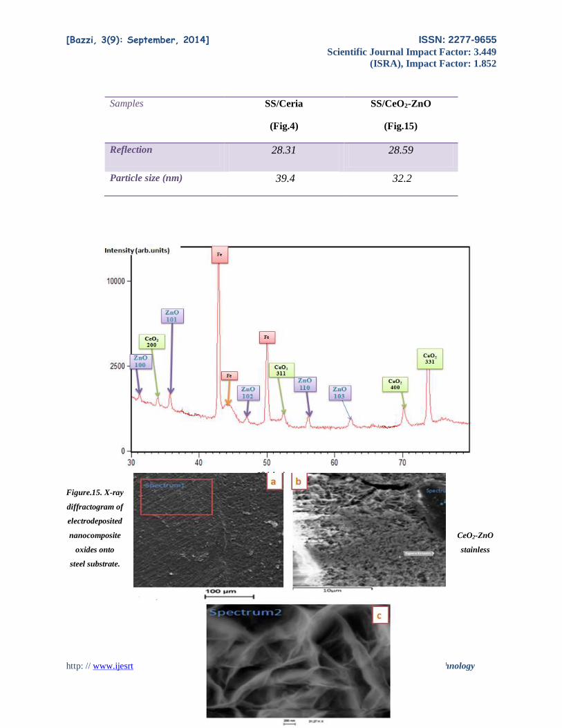
Using less current density (2mA/cm2), XRD patterns
of CeO2-ZnO nanocomposite film indicate that this
type of binary oxide demonstrates the same property
and trend as other type discussed in previous section.
Table.3. lists the particle sizes of nanocomposite
leads to a relatively more (200) oriented film (figure
15) with particle size of 32 nm. To validate the
incorporation of ZnO within ceria oxide films, both
film surface and cross-section were subjected to SEM
/ EDX detection. The surface (Figure 16) exhibits a
thick construction. Under high magnification, the
layered structure of CeO2-ZnO binary oxide can be
seen. For this system, the film is quite homogeneous,
with no cracks on its surface, and has the same
morphology as pure ceria film (Figure.7c).
Dispersive X-ray analysis reveals elemental Ce, Zn,
and O were present in the film (figure 17).
Table.3. CeO2 Particle size vs. content of ZnO in nanocomposite
[Bazzi, 3(9): September, 2014] ISSN: 2277-9655
Scientific Journal Impact Factor: 3.449
(ISRA), Impact Factor: 1.852
http: // www.ijesrt.com (C)International Journal of Engineering Sciences & Research Technology
[185]
Samples SS/Ceria
(Fig.4)
SS/CeO2-ZnO
(Fig.15)
Reflection 28.31 28.59
Particle size (nm) 39.4 32.2
Figure.15. X-ray
diffractogram of
electrodeposited
nanocomposite CeO2-ZnO
oxides onto stainless
steel substrate.

[Bazzi, 3(9): September, 2014] ISSN: 2277-9655
Scientific Journal Impact Factor: 3.449
(ISRA), Impact Factor: 1.852
http: // www.ijesrt.com (C)International Journal of Engineering Sciences & Research Technology
[186]
Figure.16. SEM micrographs for the deposits of CeO2-ZnO and a zoom of boxed area (spectrum 1&2)
Figure.17. EDS Spectrum of CeO2-ZnO in the boxed area (Figure.16)
From the results, the cathodic electrodeposition of
CeO2-ZnO was confirmed by all analysis. CeO2 kept
its cubic form. The surface of deposit does not
present any network of cracks, which presents a
[Bazzi, 3(9): September, 2014] ISSN: 2277-9655
Scientific Journal Impact Factor: 3.449
(ISRA), Impact Factor: 1.852
http: // www.ijesrt.com (C)International Journal of Engineering Sciences & Research Technology
[187]
promising result. ZnO played an important role in the
CeO2-ZnO system. Normally, ceria had high activity,
good stability and may find application in the
catalysis field. The elaboration of CeO2-ZnO
nanocomposite oxides can help to increase the
catalytic properties of ceria, especially as ZnO was
able to overcome the problem of cracking. The
electrocatalytic efficiency test of CeO2-ZnO binary
oxide will be investigated.
Conclusion This study has shown that CeO2, CeO2-ZnO
and CeO2-CaO have been successfully produced by
means of cathodic electrodeposition method. The
deposition process has been quantified in
experiments performed with three kinds of substrates.
The amount of the deposited material can be
controlled by variation of deposition time, current
density and electrolyte concentration. The ceria and
the binary oxides were synthesized at room
temperature, under galvanostatic conditions. All
obtained films had a nanocrystalline structure, and
close morphology. The results were confirmed by
XRD measurement and SEM analysis. Moreover,
ZnO was found to contribute to the better
crystallinity and no cracks of ceria, this was proven
by XRD and SEM analysis.
References [1] Y. Sun, N. G. Ndifor-Angwafor, D. J. Riley, and
M. N. R. Ashfold, Chem. Phys. Lett. 43. 2006.
[2] Y. Gao, M. Nagai, T.-C. Chang, and J.-J. Shyue,
Cryst. Growth Des. vol.7. 2007.
[3] Y. Masuda, S. Wakamatsu, and K. Koumoto, J.
Eur. Ceram. Soc. vol.24. 2004.
[4] S. T. Chang, I. C. Leu, and M. H. Hon, J. Cryst.
Growth. no.273. 2004.
[5] L. Vayssieres and M. Graetzel, Angew. Chem.
Int. Ed. 43. 2004. pp. 3666.
[6] C. Levêque, Watery Ecosystems (Hachette,
1996).
[7] http:// [email protected]
[8] Shen, W.; Matsumura, Y. Journal of Molecular
Catalysis A: Chemical.2000, pp. 165-168.
[9] Xavier, K. O.; Sreekala, R.; Rashid, K. K. A.;
Yusuff, K. K. M.; Sen, B. Catalysis Today. Vol.49 .
1999, pp. 17-22.
[10] Yao, C.; Weng, H. Industrial & Engineering
Chemistry Research no.37.1998, pp.2647-2653.
[11] K.J. Feng, Y.H. Yang, Z.J. Wang, J.H. Jiang,
G.L. Shen, R.Q. Yu, Talanta no.70.2006.
[12] H. Inaba and H. Tagawa, Solid State
Ionics,1996.
[13] Wu, Z.; Huang, D.; Yang, X. Vacuum
no.51.1998, pp. 397-401.
[14] Gnanarajan, S.; Savvides, N. Thin Solid Films .
1999, pp. 124-129.
[15] Cotell, C. M.; Hirvonen, J. K. Surface and
Coatings Technology. 1996, pp. 118-124.
[16] Huang, D.; Qin, F.; Yao, Z.; Ren, Z.; et.al.
Applied Physics Letters .vol.67. 1995, pp.3725-3726.
[17] Pan, M.; Meng, G. Y.; Xin, H. W.; Chen, C. S.;
et.al. Thin Solid Films. 1998, pp. 89-93.
[18] Wang, A.; Belot, J. A.; Tobin, J. M.; Markworth,
P. R. Physica C. 1999, pp. 154-160.
[19] Pollard, K. D.; Jenkins, H. A.; Puddephatt, R. J.
Chemistry of Materials.vol.12. 2000,pp.701-710.
[20] Nigro, R. L.; Malandrino, G.; Fragalà, I. L.
Chemistry of Materials. 2001, pp. 4402-4404.
[21] Carter, W. B.; Book, G. W.; Pollery, T.
A.;Stollberg, D. W.; Hampikian, J. M. Thin Solid
Films. 1999, pp. 25-30.
[22] Chin, C. C.; Lin, R. J.; Yu, Y. C.; Wang, C. W.;
et.al. Physica C. 1996, pp. 86-92.
[23] Chin, C. C.; Lin, R. J.; Yu, Y. C.; Wang, C. W.;
et.al. IEEE Transactions on Applied
Superconductivity. Vol.7. 1997, pp. 1403-1406.
[24] Amirhaghi, S.; Li, Y. H.; Kilner, J. A.; Boyd, I.
A. Materials Science and Engineering. 1995, pp.
192-198.
[25] Shi, D. Q.; Ionescu, M.; McKinnon, J.; Dou, S.
X. Physica C. 2001, pp. 304-310.
[26] Wang, S; Wang, W; Liu, Q.; Zhang, M.; Qian,
Y. Solid State Ionics. 2000, pp. 211-215.
[27] Czerwinski, F. Szpunar Thin Solid Films. 1996,
pp.213-219.
[28] Y. Zhou, J.A. Switzer, J. Alloy Compd. pp. 237,
1996.
[29] I. Zhitomirsky, A. Petric, Mater. Lett. 1999.
[30] I. Zhitomirsky, A. Petric, Ceram. Int. 2001.
[31] P. Stefanov, G. Atanasova, D. Stoychev, Ts.
Marinova, Surf. Coat. Technol. 2004.
[32] M. El Hajji, A. Hallaoui, L. Bazzi, O. Jbara, A.
Benlhachemi, A. Tara, B.Bakiz, Int. J.
Electrochem. Sci, accepted (2014).
[33] M. Balasubramaniana, C.A. Melendresa, A.N.
Mansour, Thin Solid Films. 1999, pp. 178.
[34] L. Arurault, P. Monsang, J. Salley, R.S. Bes,
Thin Solid Films. 2004, pp.75.

[Bazzi, 3(9): September, 2014] ISSN: 2277-9655
Scientific Journal Impact Factor: 3.449
(ISRA), Impact Factor: 1.852
http: // www.ijesrt.com (C)International Journal of Engineering Sciences & Research Technology
[188]
[35] Y. Hamlaoui, F. Pedraza, C. Remazeilles, S.
Cohendoz, C. Rebere, L. Tifouti, J.Creus, Mater.
Chem. Phys. 2009, pp. 650.
[36] Li, E.B., Thompson, G.E. Situ atomic force
microscopy studies of the deposition of cerium
oxide films on regulary corrugated surfaces. J.
Electrochem. Soc., vol.146, pp.1809-1815, 1999.
[37] J.O’M. Bockris, G.A. Razumney, Fundamental
Aspects of Electrocrystallization, Plenum Press,
New York, 1967, pp. 27.
[38] B.D. Cullity, Elements of X-ray Diffraction, 2nd
ednR, Addison Wesley. Reading. MA, 1978.
[39] H.Y. Chang, H.I. Chen, J. Cryst. Growth, 2005.
[40] J. Creus, F. Brezault, C. Rébéré, M. Gadouleau,
Surf. Coat. Technol, 2006.