Edge Oxidation Effect of Chemical-Vapor-Deposition-Grown Graphene Nanoconstriction
7
Edge Oxidation Effect of Chemical-Vapor-Deposition-Grown Graphene Nanoconstriction Muhammad Waqas Iqbal, † Muhammad Zahir Iqbal, † Xiaozhan Jin, ‡ Chanyong Hwang, ‡ and Jonghwa Eom* ,† † Department of Physics and Graphene Research Institute, Sejong University, Seoul 143-747, Korea ‡ Center for Nanometrology, Korea Research Institute of Standards and Science, Daejeon 305-340, Korea ABSTRACT: The edge oxidation effects of chemical-vapor-deposition-grown graphene devices with nanoconstrictions of different sizes are presented. The effects of edge oxidation on the doping level of a nanoconstriction graphene device were identified by Raman spectroscopy and using the back-gate-voltage-dependent resistance. Strong p-type doping was observed as the size of nanoconstriction decreased. The Dirac point of the graphene device shifted toward positive voltage, and the positions of the G and 2D peaks in Raman spectroscopy shifted toward a higher wave number, indicating the p-type doping effect of the graphene device. p-type doping was lifted by deep-ultraviolet light illumination under a nitrogen atmosphere at room temperature. p-type doping was restored by deep-ultraviolet light illumination under an oxygen atmosphere at room temperature. Edge oxidation in the narrow structures explains the origin of the p-type doping effect widely observed in graphene nanodevices. KEYWORDS: graphene, edge oxidation, nanoconstriction, doping, Raman spectroscopy, transport 1. INTRODUCTION Graphene, a two-dimensional planar layer of graphite, having weak spin−orbit coupling and ballistic conduction with chirality conservation, is a promising material for both fundamental investigations and potential applications owing to its exclusive electronic properties, especially its high carrier mobility at room temperature. 1,2 Electronic, optical, and mechanical properties make graphene a promising candidate material for applications such as sensors, ultrathin membranes, and transparent and flexible electrodes. 3 Recently, large-area graphene has been synthesized by chemical vapor deposition (CVD) using a copper or nickel catalyst. CVD-grown graphene can be easily transferred to an intended substrate using poly(methyl methacrylate) (PMMA) and poly(dimethylsiloxane) at com- paratively low expense. 3−6 The doping of graphene has received much attention owing to the critical need to fabricate integrated devices with convoluted structural design such as logic circuits. In recent times, there has been strong research interest in clusters and metal adatoms on graphene, for which it is known that there is local doping and modification of the band structure. 7,8 The band structure has also been modified when graphene is patterned at nanoscale. New phenomena found in graphene- based electronic devices have given rise to extensive theoretical studies. 9 Understanding the edge effects on the device performance is important because the modern nanolithography procedure is still far from achieving ideal atomistic precision. 10,11 The edges of lithography-patterned graphene nanoribbons are rough and have disordered regions. The charge density induced by functional groups of edges should vary from edge to center. 11,12 Consequently, it is essential to gain a better understanding of the unique properties of extremely narrow graphene devices, which are associated with the effects of edge chemistry and edge states in general. Covalent attachment of chemical groups and oxidation in particular can extensively modify the electronic properties of narrow graphene. To improve the transport properties of narrow graphene devices, it is critical to recognize the foremost sources of carrier scattering and functional groups on the edges. 11,13−15 However, during standard fabrication processes employing oxygen plasma etching, an O 2 molecule mostly prefers to be adsorbed at the edge site among different chemisorption sites, where the edge trapping implies that the graphene edges become oxidized. 16−18 The effects of edge roughness and edge oxidation on the electronic structures and properties of nanopatterned graphene have already been reported on the theoretical stage. 9,14−18 Theories showed that the electronic Received: December 20, 2013 Accepted: February 24, 2014 Research Article www.acsami.org © XXXX American Chemical Society A dx.doi.org/10.1021/am405885c | ACS Appl. Mater. Interfaces XXXX, XXX, XXX−XXX
-
Upload
independent -
Category
Documents
-
view
2 -
download
0
Transcript of Edge Oxidation Effect of Chemical-Vapor-Deposition-Grown Graphene Nanoconstriction
Edge Oxidation Effect of Chemical-Vapor-Deposition-GrownGraphene NanoconstrictionMuhammad Waqas Iqbal,† Muhammad Zahir Iqbal,† Xiaozhan Jin,‡ Chanyong Hwang,‡
and Jonghwa Eom*,†
†Department of Physics and Graphene Research Institute, Sejong University, Seoul 143-747, Korea‡Center for Nanometrology, Korea Research Institute of Standards and Science, Daejeon 305-340, Korea
ABSTRACT: The edge oxidation effects of chemical-vapor-deposition-grown graphene devices with nanoconstrictions ofdifferent sizes are presented. The effects of edge oxidation on the doping level of a nanoconstriction graphene device wereidentified by Raman spectroscopy and using the back-gate-voltage-dependent resistance. Strong p-type doping was observed asthe size of nanoconstriction decreased. The Dirac point of the graphene device shifted toward positive voltage, and the positionsof the G and 2D peaks in Raman spectroscopy shifted toward a higher wave number, indicating the p-type doping effect of thegraphene device. p-type doping was lifted by deep-ultraviolet light illumination under a nitrogen atmosphere at roomtemperature. p-type doping was restored by deep-ultraviolet light illumination under an oxygen atmosphere at room temperature.Edge oxidation in the narrow structures explains the origin of the p-type doping effect widely observed in graphene nanodevices.
KEYWORDS: graphene, edge oxidation, nanoconstriction, doping, Raman spectroscopy, transport
1. INTRODUCTION
Graphene, a two-dimensional planar layer of graphite, havingweak spin−orbit coupling and ballistic conduction with chiralityconservation, is a promising material for both fundamentalinvestigations and potential applications owing to its exclusiveelectronic properties, especially its high carrier mobility at roomtemperature.1,2 Electronic, optical, and mechanical propertiesmake graphene a promising candidate material for applicationssuch as sensors, ultrathin membranes, and transparent andflexible electrodes.3 Recently, large-area graphene has beensynthesized by chemical vapor deposition (CVD) using acopper or nickel catalyst. CVD-grown graphene can be easilytransferred to an intended substrate using poly(methylmethacrylate) (PMMA) and poly(dimethylsiloxane) at com-paratively low expense.3−6
The doping of graphene has received much attention owingto the critical need to fabricate integrated devices withconvoluted structural design such as logic circuits. In recenttimes, there has been strong research interest in clusters andmetal adatoms on graphene, for which it is known that there islocal doping and modification of the band structure.7,8 Theband structure has also been modified when graphene ispatterned at nanoscale. New phenomena found in graphene-based electronic devices have given rise to extensive theoreticalstudies.9 Understanding the edge effects on the deviceperformance is important because the modern nanolithography
procedure is still far from achieving ideal atomisticprecision.10,11 The edges of lithography-patterned graphenenanoribbons are rough and have disordered regions. Thecharge density induced by functional groups of edges shouldvary from edge to center.11,12 Consequently, it is essential togain a better understanding of the unique properties ofextremely narrow graphene devices, which are associated withthe effects of edge chemistry and edge states in general.Covalent attachment of chemical groups and oxidation inparticular can extensively modify the electronic properties ofnarrow graphene. To improve the transport properties ofnarrow graphene devices, it is critical to recognize the foremostsources of carrier scattering and functional groups on theedges.11,13−15
However, during standard fabrication processes employingoxygen plasma etching, an O2 molecule mostly prefers to beadsorbed at the edge site among different chemisorption sites,where the edge trapping implies that the graphene edgesbecome oxidized.16−18 The effects of edge roughness and edgeoxidation on the electronic structures and properties ofnanopatterned graphene have already been reported on thetheoretical stage.9,14−18 Theories showed that the electronic
Received: December 20, 2013Accepted: February 24, 2014
Research Article
www.acsami.org
© XXXX American Chemical Society A dx.doi.org/10.1021/am405885c | ACS Appl. Mater. Interfaces XXXX, XXX, XXX−XXX
structure and transport properties of graphene nanoribbons arestrongly affected by edge disorder and various functional groupspresent at edges. In fact, theories focused on graphenenanoribbons where the width is only a few nanometers. Theedge effects of extremely narrow graphene devices remainexperimentally unexplored.In this paper, we show that the effect of edge oxidation
increases with a decrease in the width of nanoconstriction. Wehave fabricated nanoconstriction devices of CVD-growngraphene and investigated the characteristics of devices byRaman spectroscopy and transport measurement. We foundthat the doping effect is locally dominant at the edges ofgraphene devices with nanoconstriction and that the dopingcan be controlled through deep-ultraviolet (DUV) lightillumination with a gas flow.
2. EXPERIMENTAL SECTIONA graphene film was grown on 25-μm-thick copper foils from AlfaAesar (99.8% pure) via thermal CVD. A mechanically polished andelectropolished copper foil was inserted into a thermal CVD furnace.The furnace was evacuated to ∼10−4 Torr, and the temperature rose to1010 °C with H2 gas flow (∼10−2 Torr). After the temperaturebecame stable at 1010 °C, both CH4 [20 standard cubic centimetersper minute (sccm)] and H2 (5 sccm) were injected into the furnace tosynthesize the graphene for 8 min. After graphene synthesis, thesample was cooled at a rate of 50 °C/min to room temperature.3,4
Graphene films were transferred onto Si/SiO2 wafers as follows.Copper foil was etched in an aqueous solution of ammoniumpersulfate. The surface of the graphene was spin-coated with PMMA,and the sample was then baked at 70 °C for 10 min. The PMMAcoating was applied to prevent graphene films from cracking andfolding during transfer to a desired substrate. PMMA/graphene filmwas washed with deionized water after the copper foil had beencompletely dissolved, and it was then transferred onto the Si/SiO2wafer. The PMMA film was removed with an organic solvent. Thegraphene sample was subsequently cleaned in isopropyl alcohol anddried in a N2 gas flow.
3,4
We fabricated graphene devices by employing photolithography, e-beam lithography, and oxygen plasma etching. Large electrode patternswith a chromium/gold (6/30 nm) film were deposited using a thermalevaporator after standard photolithography. E-beam lithography wasthen employed to pattern a direct ohmic contact on the graphene.Nanoconstrictions were produced by e-beam lithography and oxygenplasma etching; nanoconstrictions had different sizes of 60, 80, and100 nm. The distance between contact electrodes is 5 μm, and theangle between graphene edges is 45° for all devices in this experiment.The width of the graphene ribbon is 5 μm for all nanoconstrictiondevices. A 5-μm-wide graphene strip was also fabricated as a referencedevice. The characteristics of a single-layer graphene were examined byoptical microscopy and Raman spectroscopy.Raman spectroscopy was carried out at the nanoconstriction of each
graphene device. Raman mapping was also conducted to examine aCVD-grown graphene sheet at room temperature. The laserwavelength of the Raman microspectrometer was 514 nm, and thepower was kept at less than l.0 mW to avoid a laser-induced heatingeffect. The laser spot size of Raman spectroscopy was 0.7 μm for awavelength of 514 nm. The Dirac point of each graphene device wasobserved by gate-voltage-dependent resistance measurement using afour-probe measurement configuration with a lock-in amplifier.Electrical transport measurement was also performed for graphenenanoconstriction devices after exposure to DUV light with awavelength of λ = 220 nm and an average intensity of 11 mW/cm2
in N2 gas flow for a certain time. The device was placed in a glass tube,and the glass tube was pumped to evacuate air. Then N2 gas wasintroduced into the glass tube with continuous flow. DUV light wasturned on to shine on the device in the glass tube. Figure 1a is aschematic diagram of the experimental setup of DUV lightillumination.
Raman spectroscopy provides a convenient, nondestructive, and fasttechnique for characterizing the fundamental physical properties ofvarious carbon materials, such as monolayer, bilayer, and stackedgraphenes and single-walled/multiwalled carbon nanotubes.19−21
Raman spectra of monolayer, bilayer, and multilayer graphene havetwo characteristic peaks (G and 2D). The G band is associated withthe E2g vibration mode of sp2 bonds.20−22 The 2D peak is the secondorder of the D peak and originates from a process where momentumconservation is satisfied by two phonons with opposite wavevectors.21,22 The 2D peak is always present in Raman spectra ofgraphene. For single-layer graphene, the I2D/IG ratio must be greaterthan 2, and the full width at half-maximum (fwhm) of the 2D band isabout 30 cm−1. The D peak is due to A1g-mode breathing vibrations ofsix-membered sp2 carbon rings, which are absent in puregraphene.21−24
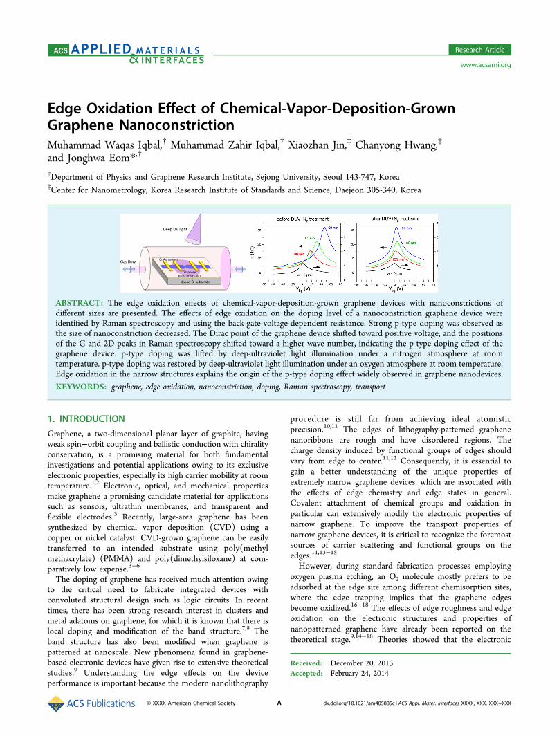
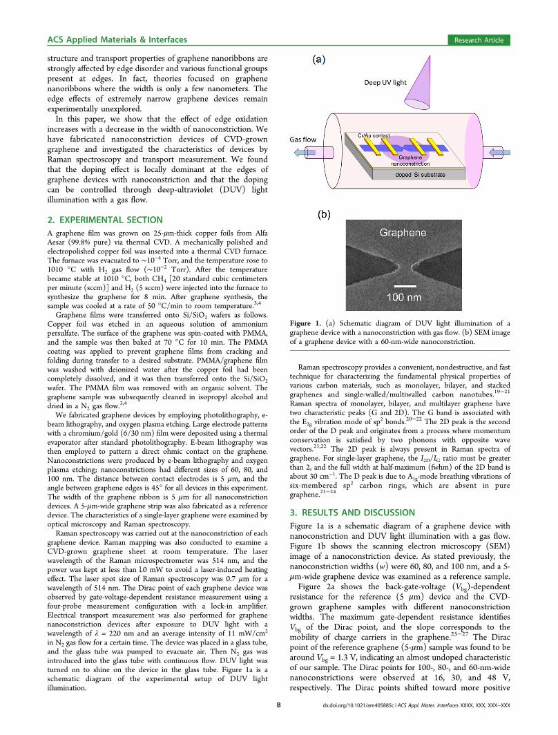
3. RESULTS AND DISCUSSIONFigure 1a is a schematic diagram of a graphene device withnanoconstriction and DUV light illumination with a gas flow.Figure 1b shows the scanning electron microscopy (SEM)image of a nanoconstriction device. As stated previously, thenanoconstriction widths (w) were 60, 80, and 100 nm, and a 5-μm-wide graphene device was examined as a reference sample.Figure 2a shows the back-gate-voltage (Vbg)-dependent
resistance for the reference (5 μm) device and the CVD-grown graphene samples with different nanoconstrictionwidths. The maximum gate-dependent resistance identifiesVbg of the Dirac point, and the slope corresponds to themobility of charge carriers in the graphene.25−27 The Diracpoint of the reference graphene (5-μm) sample was found to bearound Vbg = 1.3 V, indicating an almost undoped characteristicof our sample. The Dirac points for 100-, 80-, and 60-nm-widenanoconstrictions were observed at 16, 30, and 48 V,respectively. The Dirac points shifted toward more positive
Figure 1. (a) Schematic diagram of DUV light illumination of agraphene device with a nanoconstriction with gas flow. (b) SEM imageof a graphene device with a 60-nm-wide nanoconstriction.
ACS Applied Materials & Interfaces Research Article
dx.doi.org/10.1021/am405885c | ACS Appl. Mater. Interfaces XXXX, XXX, XXX−XXXB
gate voltages as the width of nanoconstriction decreased,indicating the p-type doping of the graphene. As thenanoconstriction width decreased, the resistance of a graphenedevice increased, and a stronger p-type doping effect wasobserved.Asymmetry is found in the Vbg-dependent resistivity of the
graphene devices (see Figure 2a). Because the band structuresof graphene for the hole and electron are symmetric, themobilities of the electron and hole are expected to be equal.Therefore, one can expect a symmetric Vbg-dependentresistivity with respect to the Dirac point. However, in normalgraphene devices, the hole mobility is higher than the electronmobility because of the different scattering cross sections forthe electron and hole by charge impurity in the relativisticdispersion.28 Because the slope of the conductivity, dσ/dVg, isproportional to mobility, the asymmetry in the Vbg-dependentresistivity has been consistently observed in graphene devices inthis paper.Figure 2b shows the gate-dependent resistances of the
graphene devices after 30 min of DUV exposure in a N2 gasflow (DUV+N2). DUV+N2 exposure of the graphene deviceshifted the Dirac point toward 0 V. The shift in the Dirac pointdue to DUV+N2 treatment is shown in Figure 2c. The Dirac
points of the reference graphene device and devices with 100-,80-, and 60-nm-wide nanoconstrictions were observed at 1.3,16, 31, and 47 V, respectively, for the as-prepared condition(before DUV+N2 treatment). After 15 min of DUV+N2exposure of the graphene devices, the Dirac points shifted to0.4, 3, 3.5, and 4 V, respectively. The Dirac points shiftedfurther to 0, 1.1, 1.9, and 3 V, respectively, after 30 min of DUV+N2 exposure. We found that exposure to DUV affects theDirac point and that the position of the Dirac point remainsalmost the same for a N2 gas flow without DUV illumination.DUV illumination should provide the energy required for thereaction of nitrogen atoms with oxygen atoms, which wereoriginally adhered to graphene. A minimum amount of energyis required to release oxygen from the surface of graphene.29−31
Figure 2d shows the gate-voltage-dependent resistance forthe graphene device with a 100-nm-wide nanoconstriction after10, 20, and 30 min of DUV exposure in an O2 gas flow (DUV+O2). The Dirac points were observed at 39, 52, and 60 V after10, 20, and 30 min of DUV+O2 treatment, respectively. Oxygenadsorption on graphene should have a p-type doping effect.The adsorption of oxygen on a graphene film has already beenstudied.32−34 However, we found that the effect of oxygendoping is more significant when graphene is exposed to DUV
Figure 2. (a) Vbg-dependent resistance for the reference (w = 5 μm) and nanoconstrictions of CVD-grown graphene. Resistance is measured withfour-probe geometry using standard lock-in amplifier techniques. The Dirac point of the reference graphene sample is around Vbg = 1.3 V, indicatingan almost undoped characteristic of pristine graphene. The arrows indicate the y-axis scale for reference and different nanoconstriction graphenesamples. The rightward arrow indicates the scale for the reference sample, whereas the leftward arrow indicates the scale for nanoconstrictiondevices. (b) Vbg-dependent resistance of the reference and nanoconstriction samples after 30 min of DUV illumination with a N2 gas flow. DUV+N2treatment results in the shift of the Dirac point toward Vbg = 0 V. (c) Dirac point as a function of the nanoconstriction width for the as-preparedgraphene and after different DUV+N2 exposure times. (d) Experiment started with the device having a 100-nm-wide nanoconstriction after 30 minof DUV+N2 treatment. DUV+O2 treatment was applied to restore the p-type doping of nanoconstriction. Vbg-dependent resistance after 10, 20, and30 min of DUV exposure in an oxygen atmosphere. The Dirac points were observed at Vbg = 39, 52, and 60 V after 10, 20, and 30 min of DUV+O2treatment, respectively.
ACS Applied Materials & Interfaces Research Article
dx.doi.org/10.1021/am405885c | ACS Appl. Mater. Interfaces XXXX, XXX, XXX−XXXC
light. DUV light provides enough energy for electrons to adsorbonto, or desorb from, the surface of graphene.Raman spectra of the nanoconstrictions and reference
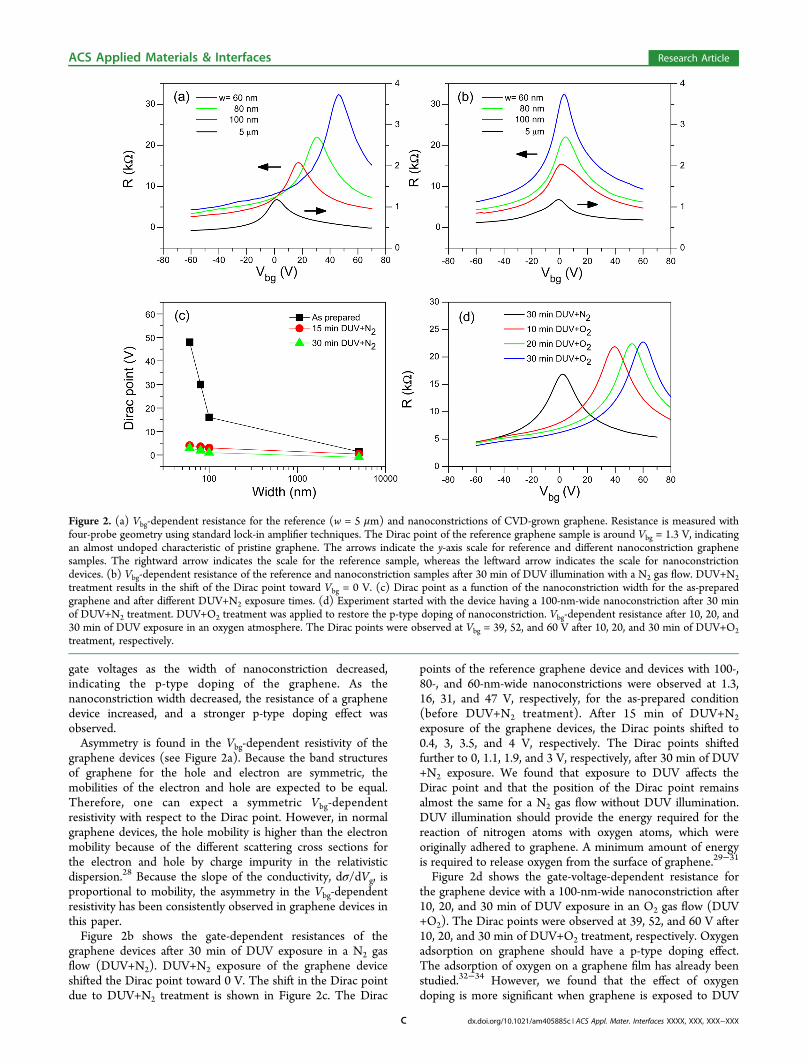
graphene are shown in Figure 3a. The Raman spectra indicatethe overall behavior of a single-layer graphene. The D peakbecame more pronounced as the width of nanoconstrictiondecreased. G and 2D peaks were observed at 1581 and 2682cm−1, respectively, for the reference graphene device. As anindication that the samples were single-layer graphenestructures, we found that the intensity of the 2D peak was 3times that of the G peak and the fwhm of the 2D band of thereference graphene was about 30 cm−1. The absence of the Dpeak in the reference graphene indicates the high quality of thereference. However, the D peak appeared for nanoconstrictiondevices, and the D-band intensity increased drastically as thewidth of nanoconstriction decreased. The observation of the Dpeak was accompanied by a pronounced D′ peak at 1624 cm−1
and a D + D′ peak around 2945 cm−1. We note that D′ and D+ D′ peaks were not observed for the reference graphene butbecame prominent for nanoconstrictions.Figure 3b shows the shift in the positions and change in the
intensities of the G and 2D peaks. While the G band wasobserved at 1581 cm−1 for the reference graphene, it was foundat 1585, 1591, and 1597 cm−1 for nanoconstriction widths of100, 80, and 60 nm, respectively. There was a blue shift of 16cm−1 in the G band for 60-nm-wide nanoconstriction relative tothe reference graphene. There was also a blue shift in the 2Dband for nanoconstrictions. While the 2D band of the referencegraphene was observed at 2682.1 cm−1, those of nano-constrictions with widths of 100, 80, and 60 nm were observedat 2686.3, 2694.2, and 2699.1 cm−1, respectively. There was ablue shift of 17 cm−1 in the peak position of the 2D band for60-nm-wide nanoconstriction relative to the referencegraphene. Figure 3c shows Lorentzian fits for the G and D′peaks. Red circles represent the experimental data, and black,blue, and green lines are the Lorentzian fits for the G, D′, andcombined peaks, respectively. The fwhm’s of the G band were16, 14, 13.1, and 11.5 cm−1 for the reference and nano-constriction widths of 100, 80, and 60 nm, respectively. Theblue shifts of the G and 2D band positions are known to beassociated with p-type doping of graphene, and doping reducesthe fwhm of the G peak.35
The blue shift of the G and 2D peaks and reduction of thefwhm of the G peak indicate a p-type doping effect, which canbe also confirmed by the electrical measurement of thegraphene device.35−41 Our experimental observations clearlyindicate the p-type doping of the graphene device whenpatterned with nanoconstriction. The doping effect is closelyrelated to the adsorption of O2 molecules at the edge ofnanoconstriction during the patterning process. During thepatterning process, the entire area is covered with PMMA sothat O2 molecules can attach mostly to the graphene patternedges. Here O2 trapping implies that the graphene edgesbecome oxidized and p-type-doped.10,11,17,18
The width of the graphene ribbon is kept the same as 5 μmfor all devices in the experiment. Therefore, the effect of thedistance between edges on edge oxidation can be seen bychanging the width of nanoconstriction. As we reduce thenanoconstriction width, electrons passing through narrowernanoconstriction are more actively affected by oxidized edges.Actually, Figure 2a shows the effect of the distance betweenedges on edge oxidation. Figure 2c shows that effect of thedistance between edges on an edge−edge-redox reaction. When
the distance between edges decreases in nanoconstriction, theinfluence by the edge oxidation (or edge-redox reaction) on thetransport properties becomes more dominant.
Figure 3. (a) Raman spectra of the as-prepared reference andnanoconstriction devices. (b) Shifts in the positions of the G and 2Dpeaks. G-band peaks in Raman spectra were observed at 1582.1,1585.3, 1591.2, and 1598.1 cm−1 for the reference (w = 5 μm) andnanoconstrictions (w = 100, 80, and 60 nm), respectively. 2D-bandpeaks in Raman spectra were observed at 2682.1, 2686.3, 2694.2, and2699.1 cm−1 for the reference (w = 5 μm) and nanoconstrictions (w =100, 80, and 60 nm), respectively. (c) Lorentzian fits for the reference(w = 5 μm) and nanoconstrictions (w = 100, 80, and 60 nm). Redcircles represent the experimental data, and black, blue, and green linesare the Lorentzian fits for the G, D′, and combined peaks, respectively.fwhm’s of the G-band peaks are 16, 14, 13.1, and 11.5 cm−1 for thereference (w = 5 μm) and nanoconstrictions (w = 100, 80, and 60nm), respectively.
ACS Applied Materials & Interfaces Research Article
dx.doi.org/10.1021/am405885c | ACS Appl. Mater. Interfaces XXXX, XXX, XXX−XXXD
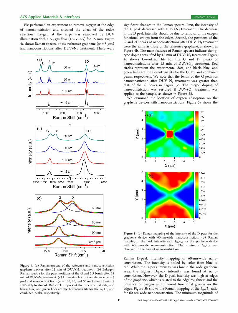
We performed an experiment to remove oxygen at the edgeof nanoconstriction and checked the effect of the redoxreaction. Oxygen at the edge was removed by DUVillumination with a N2 gas flow (DUV+N2) for 15 min. Figure4a shows Raman spectra of the reference graphene (w = 5 μm)and nanoconstrictions after DUV+N2 treatment. There were
significant changes in the Raman spectra. First, the intensity ofthe D peak decreased with DUV+N2 treatment. The decreasein the D peak intensity should be due to removal of the oxygenfunctional groups from the edges. Second, the positions of theG and 2D peaks of nanoconstrictions after DUV+N2 treatmentwere the same as those of the reference graphene, as shown inFigure 4b. The main features of Raman spectra indicate that p-type doping was lifted by 15 min of DUV+N2 treatment. Figure4c shows Lorentzian fits for the G and D′ peaks ofnanoconstrictions after 15 min of DUV+N2 treatment. Redcircles represent the experimental data, and black, blue, andgreen lines are the Lorentzian fits for the G, D′, and combinedpeaks, respectively. We note that the fwhm of the G peak fornanoconstriction after DUV+N2 treatment was greater thanthat of the G peaks in Figure 3c. The p-type doping ofnanoconstriction was restored if DUV+O2 treatment wasapplied to the sample, as shown in Figure 2d.We examined the location of oxygen adsorption on the
graphene devices with nanoconstrictions. Figure 5a shows the
Raman D-peak intensity mapping of 60-nm-wide nano-constriction. The intensity is scaled by color from blue tored. While the D-peak intensity was low in the wide graphenearea, the highest D-peak intensity was found at nano-constriction. However, the D-peak intensity was high at edgesof the graphene, which is related to the edge roughness and thepresence of oxygen and different functional groups on theedges. Figure 5b shows the Raman mapping of the I2D/IG ratiofor 60-nm-wide nanoconstriction. The minimum magnitude of
Figure 4. (a) Raman spectra of the reference and nanoconstrictiongraphene devices after 15 min of DUV+N2 treatment. (b) EnlargedRaman spectra for the peak positions of the G and 2D bands after 15min of DUV+N2 treatment. (c) Lorentzian fits for the reference (w = 5μm) and nanoconstrictions (w = 100, 80, and 60 nm) after 15 min ofDUV+N2 treatment. Red circles represent the experimental data, andblack, blue, and green lines are the Lorentzian fits for the G, D′, andcombined peaks, respectively.
Figure 5. (a) Raman mapping of the intensity of the D peak for thegraphene device with 60-nm-wide nanoconstriction. (b) Ramanmapping of the peak intensity ratio I2D/IG for the graphene devicewith 60-nm-wide nanoconstriction. The minimum I2D/IG wasobserved in the area of nanoconstriction.
ACS Applied Materials & Interfaces Research Article
dx.doi.org/10.1021/am405885c | ACS Appl. Mater. Interfaces XXXX, XXX, XXX−XXXE
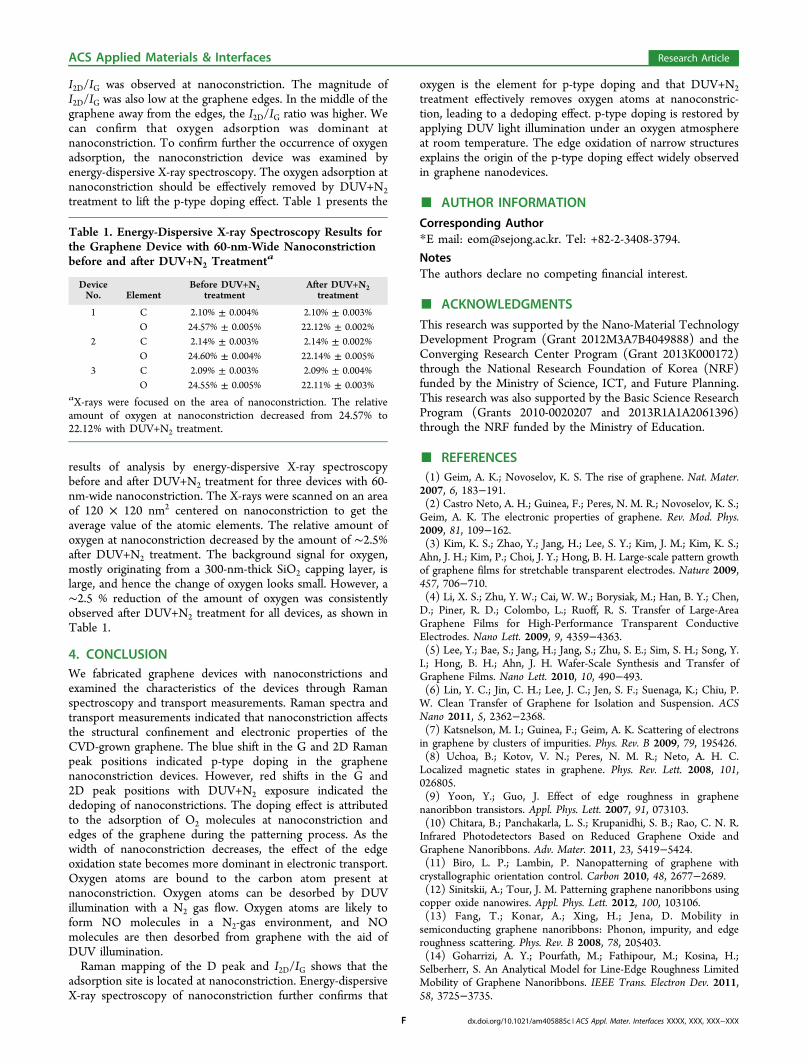
I2D/IG was observed at nanoconstriction. The magnitude ofI2D/IG was also low at the graphene edges. In the middle of thegraphene away from the edges, the I2D/IG ratio was higher. Wecan confirm that oxygen adsorption was dominant atnanoconstriction. To confirm further the occurrence of oxygenadsorption, the nanoconstriction device was examined byenergy-dispersive X-ray spectroscopy. The oxygen adsorption atnanoconstriction should be effectively removed by DUV+N2treatment to lift the p-type doping effect. Table 1 presents the
results of analysis by energy-dispersive X-ray spectroscopybefore and after DUV+N2 treatment for three devices with 60-nm-wide nanoconstriction. The X-rays were scanned on an areaof 120 × 120 nm2 centered on nanoconstriction to get theaverage value of the atomic elements. The relative amount ofoxygen at nanoconstriction decreased by the amount of ∼2.5%after DUV+N2 treatment. The background signal for oxygen,mostly originating from a 300-nm-thick SiO2 capping layer, islarge, and hence the change of oxygen looks small. However, a∼2.5 % reduction of the amount of oxygen was consistentlyobserved after DUV+N2 treatment for all devices, as shown inTable 1.
4. CONCLUSIONWe fabricated graphene devices with nanoconstrictions andexamined the characteristics of the devices through Ramanspectroscopy and transport measurements. Raman spectra andtransport measurements indicated that nanoconstriction affectsthe structural confinement and electronic properties of theCVD-grown graphene. The blue shift in the G and 2D Ramanpeak positions indicated p-type doping in the graphenenanoconstriction devices. However, red shifts in the G and2D peak positions with DUV+N2 exposure indicated thededoping of nanoconstrictions. The doping effect is attributedto the adsorption of O2 molecules at nanoconstriction andedges of the graphene during the patterning process. As thewidth of nanoconstriction decreases, the effect of the edgeoxidation state becomes more dominant in electronic transport.Oxygen atoms are bound to the carbon atom present atnanoconstriction. Oxygen atoms can be desorbed by DUVillumination with a N2 gas flow. Oxygen atoms are likely toform NO molecules in a N2-gas environment, and NOmolecules are then desorbed from graphene with the aid ofDUV illumination.Raman mapping of the D peak and I2D/IG shows that the
adsorption site is located at nanoconstriction. Energy-dispersiveX-ray spectroscopy of nanoconstriction further confirms that
oxygen is the element for p-type doping and that DUV+N2treatment effectively removes oxygen atoms at nanoconstric-tion, leading to a dedoping effect. p-type doping is restored byapplying DUV light illumination under an oxygen atmosphereat room temperature. The edge oxidation of narrow structuresexplains the origin of the p-type doping effect widely observedin graphene nanodevices.
■ AUTHOR INFORMATION
Corresponding Author*E mail: [email protected]. Tel: +82-2-3408-3794.
NotesThe authors declare no competing financial interest.
■ ACKNOWLEDGMENTS
This research was supported by the Nano-Material TechnologyDevelopment Program (Grant 2012M3A7B4049888) and theConverging Research Center Program (Grant 2013K000172)through the National Research Foundation of Korea (NRF)funded by the Ministry of Science, ICT, and Future Planning.This research was also supported by the Basic Science ResearchProgram (Grants 2010-0020207 and 2013R1A1A2061396)through the NRF funded by the Ministry of Education.
■ REFERENCES(1) Geim, A. K.; Novoselov, K. S. The rise of graphene. Nat. Mater.2007, 6, 183−191.(2) Castro Neto, A. H.; Guinea, F.; Peres, N. M. R.; Novoselov, K. S.;Geim, A. K. The electronic properties of graphene. Rev. Mod. Phys.2009, 81, 109−162.(3) Kim, K. S.; Zhao, Y.; Jang, H.; Lee, S. Y.; Kim, J. M.; Kim, K. S.;Ahn, J. H.; Kim, P.; Choi, J. Y.; Hong, B. H. Large-scale pattern growthof graphene films for stretchable transparent electrodes. Nature 2009,457, 706−710.(4) Li, X. S.; Zhu, Y. W.; Cai, W. W.; Borysiak, M.; Han, B. Y.; Chen,D.; Piner, R. D.; Colombo, L.; Ruoff, R. S. Transfer of Large-AreaGraphene Films for High-Performance Transparent ConductiveElectrodes. Nano Lett. 2009, 9, 4359−4363.(5) Lee, Y.; Bae, S.; Jang, H.; Jang, S.; Zhu, S. E.; Sim, S. H.; Song, Y.I.; Hong, B. H.; Ahn, J. H. Wafer-Scale Synthesis and Transfer ofGraphene Films. Nano Lett. 2010, 10, 490−493.(6) Lin, Y. C.; Jin, C. H.; Lee, J. C.; Jen, S. F.; Suenaga, K.; Chiu, P.W. Clean Transfer of Graphene for Isolation and Suspension. ACSNano 2011, 5, 2362−2368.(7) Katsnelson, M. I.; Guinea, F.; Geim, A. K. Scattering of electronsin graphene by clusters of impurities. Phys. Rev. B 2009, 79, 195426.(8) Uchoa, B.; Kotov, V. N.; Peres, N. M. R.; Neto, A. H. C.Localized magnetic states in graphene. Phys. Rev. Lett. 2008, 101,026805.(9) Yoon, Y.; Guo, J. Effect of edge roughness in graphenenanoribbon transistors. Appl. Phys. Lett. 2007, 91, 073103.(10) Chitara, B.; Panchakarla, L. S.; Krupanidhi, S. B.; Rao, C. N. R.Infrared Photodetectors Based on Reduced Graphene Oxide andGraphene Nanoribbons. Adv. Mater. 2011, 23, 5419−5424.(11) Biro, L. P.; Lambin, P. Nanopatterning of graphene withcrystallographic orientation control. Carbon 2010, 48, 2677−2689.(12) Sinitskii, A.; Tour, J. M. Patterning graphene nanoribbons usingcopper oxide nanowires. Appl. Phys. Lett. 2012, 100, 103106.(13) Fang, T.; Konar, A.; Xing, H.; Jena, D. Mobility insemiconducting graphene nanoribbons: Phonon, impurity, and edgeroughness scattering. Phys. Rev. B 2008, 78, 205403.(14) Goharrizi, A. Y.; Pourfath, M.; Fathipour, M.; Kosina, H.;Selberherr, S. An Analytical Model for Line-Edge Roughness LimitedMobility of Graphene Nanoribbons. IEEE Trans. Electron Dev. 2011,58, 3725−3735.
Table 1. Energy-Dispersive X-ray Spectroscopy Results forthe Graphene Device with 60-nm-Wide Nanoconstrictionbefore and after DUV+N2 Treatmenta
DeviceNo. Element
Before DUV+N2treatment
After DUV+N2treatment
1 C 2.10% ± 0.004% 2.10% ± 0.003%O 24.57% ± 0.005% 22.12% ± 0.002%
2 C 2.14% ± 0.003% 2.14% ± 0.002%O 24.60% ± 0.004% 22.14% ± 0.005%
3 C 2.09% ± 0.003% 2.09% ± 0.004%O 24.55% ± 0.005% 22.11% ± 0.003%
aX-rays were focused on the area of nanoconstriction. The relativeamount of oxygen at nanoconstriction decreased from 24.57% to22.12% with DUV+N2 treatment.
ACS Applied Materials & Interfaces Research Article
dx.doi.org/10.1021/am405885c | ACS Appl. Mater. Interfaces XXXX, XXX, XXX−XXXF
(15) Yazdanpanah, A.; Pourfath, M.; Fathipour, M.; Kosina, H.;Selberherr, S. A Numerical Study of Line-Edge Roughness Scatteringin Graphene Nanoribbons. IEEE Trans. Electron Dev. 2012, 59, 433−440.(16) Hod, O.; Barone, V.; Peralta, J. E.; Scuseria, G. E. Enhancedhalf-metallicity in edge-oxidized zigzag graphene nanoribbons. NanoLett. 2007, 7, 2295−2299.(17) Lee, G.; Cho, K. Electronic structures of zigzag graphenenanoribbons with edge hydrogenation and oxidation. Phys. Rev. B2009, 79, 165440.(18) Yu, S. S.; Zheng, W. T.; Jiang, Q. Oxidation of GrapheneNanoribbon by Molecular Oxygen. IEEE Trans. Nanotechnol. 2008, 7,628−635.(19) Dresselhaus, M. S.; Jorio, A.; Hofmann, M.; Dresselhaus, G.;Saito, R. Perspectives on Carbon Nanotubes and Graphene RamanSpectroscopy. Nano Lett. 2010, 10, 751−758.(20) Ferrari, A. C. Raman spectroscopy of graphene and graphite:Disorder, electron−phonon coupling, doping and nonadiabatic effects.Solid State Commun. 2007, 143, 47−57.(21) Dresselhaus, M. S.; Dresselhaus, G.; Saito, R.; Jorio, A. Ramanspectroscopy of carbon nanotubes. Phys. Rep. 2005, 409, 47−99.(22) Niyogi, S.; Bekyarova, E.; Itkis, M. E.; Zhang, H.; Shepperd, K.;Hicks, J.; Sprinkle, M.; Berger, C.; Lau, C. N.; Deheer, W. A.Spectroscopy of covalently functionalized graphene. Nano Lett. 2010,10, 4061−4066.(23) Ferrari, A. C.; Meyer, J. C.; Scardaci, V.; Casiraghi, C.; Lazzeri,M.; Mauri, F.; Piscanec, S.; Jiang, D.; Novoselov, K. S.; Roth, S.; Geim,A. K. Raman spectrum of graphene and graphene layers. Phys. Rev.Lett. 2006, 97, 187401.(24) Kalbac, M.; Reina-Cecco, A.; Farhat, H.; Kong, J.; Kavan, L.;Dresselhaus, M. S. The Influence of Strong Electron and Hole Dopingon the Raman Intensity of Chemical Vapor-Deposition Graphene.ACS Nano 2010, 4, 6055−6063.(25) Tan, Y. W.; Zhang, Y.; Bolotin, K.; Zhao, Y.; Adam, S.; Hwang,E. H.; Das Sarma, S.; Stormer, H. L.; Kim, P. Measurement ofscattering rate and minimum conductivity in graphene. Phys. Rev. Lett.2007, 99, 246803.(26) Morozov, S. V.; Novoselov, K. S.; Katsnelson, M. I.; Schedin, F.;Elias, D. C.; Jaszczak, J. A.; Geim, A. K. Giant intrinsic carriermobilities in graphene and its bilayer. Phys. Rev. Lett. 2008, 100,016602.(27) Chen, J. H.; Jang, C.; Adam, S.; Fuhrer, M. S.; Williams, E. D.;Ishigami, M. Charged-impurity scattering in graphene. Nat. Phys. 2008,4, 377−381.(28) Novikov, D. Numbers of donors and acceptors from transportmeasurements in graphene. Appl. Phys. Lett. 2007, 91, 102102.(29) Dai, J. Y.; Yuan, J. M. Modulating the electronic and magneticstructures of P-doped graphene by molecule doping. J. Phys.: Condens.Matter 2010, 22, 225501.(30) Chen, Y.; Gao, B.; Zhao, J. X.; Cai, Q. H.; Fu, H. G. Si-dopedgraphene: an ideal sensor for NO- or NO2-detection and metal-freecatalyst for N2O-reduction. J. Mol. Model. 2012, 18, 2043−2054.(31) Nourbakhsh, A.; Cantoro, M.; Klekachev, A. V.; Pourtois, G.;Vosch, T.; Hofkens, J.; van der Veen, M. H.; Heyns, M. M.; De Gendt,S.; Sels, B. F. Single Layer vs Bilayer Graphene: A Comparative Studyof the Effects of Oxygen Plasma Treatment on Their Electronic andOptical Properties. J. Phys. Chem. C 2011, 115, 16619−16624.(32) Batzill, M. The surface science of graphene: Metal interfaces,CVD synthesis, nanoribbons, chemical modifications, and defects. Surf.Sci. Rep. 2012, 67, 83−115.(33) Yu, L.; Pan, X. L.; Cao, X. M.; Hu, P.; Bao, X. H. Oxygenreduction reaction mechanism on nitrogen-doped graphene: A densityfunctional theory study. J. Catal. 2011, 282, 183−190.(34) Zhang, L. P.; Niu, J. B.; Dai, L.; Xia, Z. H. Effect ofMicrostructure of Nitrogen-Doped Graphene on Oxygen ReductionActivity in Fuel Cells. Langmuir 2012, 28, 7542−7550.(35) Das, A.; Pisana, S.; Chakraborty, B.; Piscanec, S.; Saha, S. K.;Waghmare, U. V.; Novoselov, K. S.; Krishnamurthy, H. R.; Geim, A.K.; Ferrari, A. C.; Sood, A. K. Monitoring dopants by Raman scattering
in an electrochemically top-gated graphene transistor. Nat. Nano-technol. 2008, 3, 210−215.(36) Casiraghi, C. Probing disorder and charged impurities ingraphene by Raman spectroscopy. Phys. Status Solidi R 2009, 3, 175−177.(37) Heydrich, S.; Hirmer, M.; Preis, C.; Korn, T.; Eroms, J.; Weiss,D.; Schuller, C. Scanning Raman spectroscopy of graphene antidotlattices: Evidence for systematic p-type doping. Appl. Phys. Lett. 2010,97, 043113.(38) Lee, J.; Novoselov, K. S.; Shin, H. S. Interaction between Metaland Graphene: Dependence on the Layer Number of Graphene. ACSNano 2011, 5, 608−612.(39) Wang, W. X.; Liang, S. H.; Yu, T.; Li, D. H.; Li, Y. B.; Han, X. F.The study of interaction between graphene and metals by Ramanspectroscopy. J. Appl. Phys. 2011, 109, 07c501.(40) Ryu, S.; Liu, L.; Berciaud, S.; Yu, Y. J.; Liu, H. T.; Kim, P.; Flynn,G. W.; Brus, L. E. Atmospheric Oxygen Binding and Hole Doping inDeformed Graphene on a SiO2 Substrate. Nano Lett. 2010, 10, 4944−4951.(41) Iqbal, M. W.; Singh, A. K.; Iqbal, M. Z.; Eom, J. Ramanfingerprint of doping due to metal adsorbates on graphene. J. Phys.:Condens. Matter 2012, 24, 3335301.
ACS Applied Materials & Interfaces Research Article
dx.doi.org/10.1021/am405885c | ACS Appl. Mater. Interfaces XXXX, XXX, XXX−XXXG