Dual-Band Microwave Device Design - CiteSeerX
51
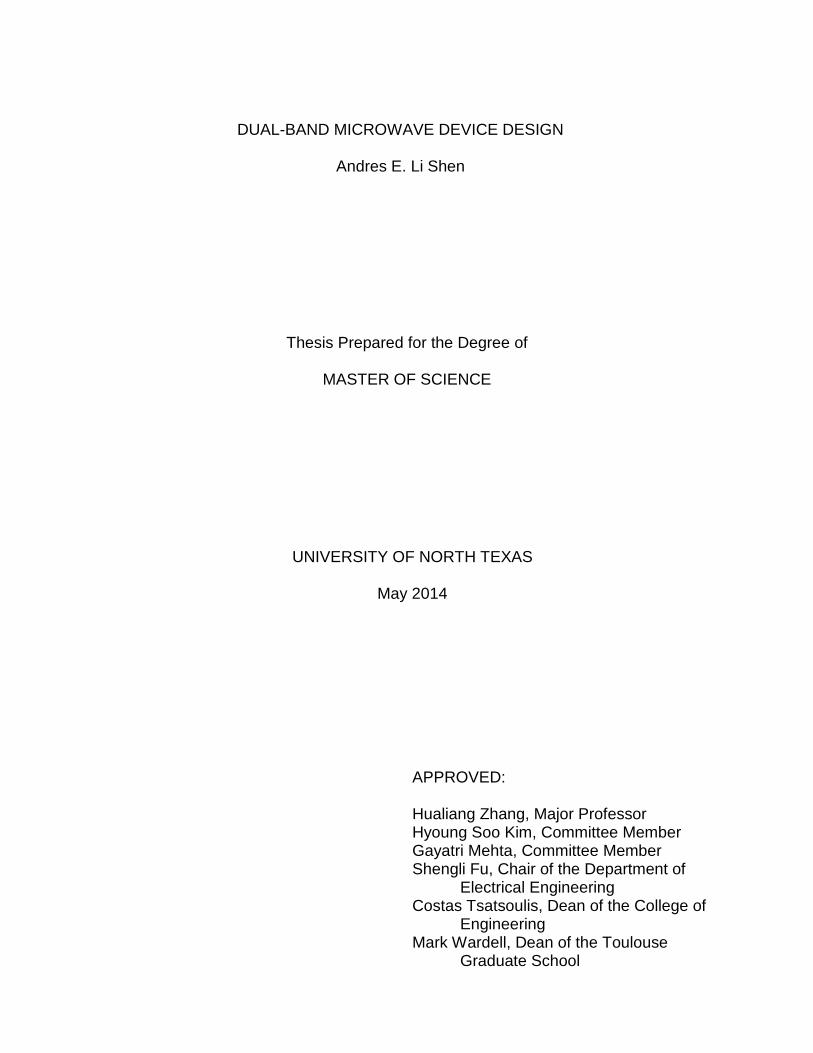
APPROVED: Hualiang Zhang, Major Professor Hyoung Soo Kim, Committee Member Gayatri Mehta, Committee Member Shengli Fu, Chair of the Department of Electrical Engineering Costas Tsatsoulis, Dean of the College of Engineering Mark Wardell, Dean of the Toulouse Graduate School DUAL-BAND MICROWAVE DEVICE DESIGN Andres E. Li Shen Thesis Prepared for the Degree of MASTER OF SCIENCE UNIVERSITY OF NORTH TEXAS May 2014
-
Upload
khangminh22 -
Category
Documents
-
view
0 -
download
0
Transcript of Dual-Band Microwave Device Design - CiteSeerX
APPROVED: Hualiang Zhang, Major Professor Hyoung Soo Kim, Committee Member Gayatri Mehta, Committee Member Shengli Fu, Chair of the Department of
Electrical Engineering Costas Tsatsoulis, Dean of the College of
Engineering Mark Wardell, Dean of the Toulouse
Graduate School
DUAL-BAND MICROWAVE DEVICE DESIGN
Andres E. Li Shen
Thesis Prepared for the Degree of
MASTER OF SCIENCE
UNIVERSITY OF NORTH TEXAS
May 2014
Li Shen, Andres E. Dual-Band Microwave Device Design. Master of Science
(Electrical Engineering), May 2014, 45 pp., 31 illustrations, references, 61 titles.
This thesis presents a brief introduction to microwave components and
technology. It also presents two novel dual-band designs, their analysis, topology,
simulation and fabrication. In chapter 2, a novel dual-band bandpass filter using
asymmetric stub-loaded stepped-impedance resonators (SLSIRs) operating at 1 and
2.6 GHz is shown. This type of design applies suitable arrangements to improve the
filter’s performance. Then, in chapter 3, a novel dual-band balun (transforms
unbalanced input signals to balanced output signals or vice versa) operating at 1.1 and
2 GHz with flexible frequency ratios is presented, which has more advantages in
microwave applications. Then, conclusion and future works are discussed in chapter 4.

Copyright 2014
by
Andres E. Li Shen
ii

ACKNOWLEDGEMENTS
I would like to thank my advisor and mentor Dr. Hualiang Zhang for all his
encouragement, help, knowledge, and motivation over the past two years. His passion
for RF and Microwave Engineering has become a motivation for me to go on in this
field. I also, would like to thank my thesis committee members, Dr. Hyoung Soo Kim,
and Dr. Gayatri Mehta for their time and support.
Finally, I would like to thank my family, friends, and lab mates for all their support,
care, and cherishing during this stage of my life.
iii
TABLE OF CONTENTS
Page
ACKNOWLEDGEMENTS ............................................................................................... iii
Chapters
1. BACKGROUND ......................................................................................................... 1
1.1. Introduction..................................................................................................... ......1
1.2. Dual-band Components and Properties .............................................................. 2
1.3. An Introduction to Filters ...................................................................................... 4
1.4. An Introduction to Baluns .................................................................................... 5
1.5. Overview of Thesis .............................................................................................. 6
2. A NOVEL DUAL-BAND BANDPASS FILTER USING ASYMMETRIC STUB-
LOADED STEPPED-IMPEDANCE RESONATORS .................................................. 8
2.1. Introduction .......................................................................................................... 8
2.2. Theoretical Analysis ............................................................................................ 9
2.3. Simulated and Experimental Results ................................................................. 13
2.4. Conclusion ......................................................................................................... 19
3. A NOVEL DUAL-BAND BALUN WITH FLEXIBLE FREQUENCY RATIOS ............. 21
3.1. Introduction ........................................................................................................ 21
3.2. Theoretical Analysis .......................................................................................... 22
3.3. Simulated and Experimental Results ................................................................. 28
3.4. Conclusion ......................................................................................................... 34
4. CONCLUSION AND FUTURE WORK ..................................................................... 36
4.1. Conclusion ......................................................................................................... 36
iv

4.2. Future Work ....................................................................................................... 36
REFERENCES .............................................................................................................. 38
v
CHAPTER 1
BACKGROUND
1.1 Introduction
The electromagnetic (EM) spectrum consists of all the wavelengths from radio
waves to gamma rays. Microwaves as part of the EM spectrum are of particular
importance nowadays. Every day, we are constantly using some electronic apparatus
which require microwave components (i.e. cellphones, computers, routers, etc.) and
these have become part of our daily lives demanding for smaller, faster, and lighter
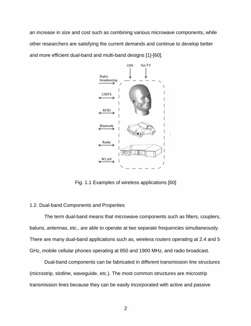
products [1]-[60] as seen in Fig. 1.1. Microwaves are EM waves with wavelengths
varying from 1mm to 1m, or equivalent to a frequency range from 300 MHz to 300 GHz
[1]-[2].
The continuous advances in communication and wireless systems have created
new challenges for the design of radio frequency (RF) and microwave components to
improve in various areas such as: size, cost, bandwidth, performance, and weight.
Some of the important components for microwave and RF applications are resonators,
filters, couplers, baluns, patch antennas, etc. Additionally, as technology is moving
forward, certain applications require multiple operating frequencies bands and broader
bandwidth causing the need for smaller, lighter, and high performance dual-band and
multi-band component designs. For instance, wireless local area network (WLAN),
global system mobile communications (GSM), worldwide interoperability for microwave
access (WiMax), and the industrial, scientific, and medical (ISM) radio operate at
multiple frequencies and have very broad bandwidths. Several design of filters and
baluns have been proposed to meet the current multi-band demands. Some may lead to
1
an increase in size and cost such as combining various microwave components, while
other researchers are satisfying the current demands and continue to develop better
and more efficient dual-band and multi-band designs [1]-[60].
Fig. 1.1 Examples of wireless applications [60]
1.2. Dual-band Components and Properties
The term dual-band means that microwave components such as filters, couplers,
baluns, antennas, etc., are able to operate at two separate frequencies simultaneously.
There are many dual-band applications such as, wireless routers operating at 2.4 and 5
GHz, mobile cellular phones operating at 850 and 1900 MHz, and radio broadcast.
Dual-band components can be fabricated in different transmission line structures
(microstrip, slotline, waveguide, etc.). The most common structures are microstrip
transmission lines because they can be easily incorporated with active and passive
2
microwave components and be fabricated through photolithographic process (“a
process whereby integrated and printed circuits are produced by photographing the
circuit pattern on a photosensitive substrate and chemically etching away the
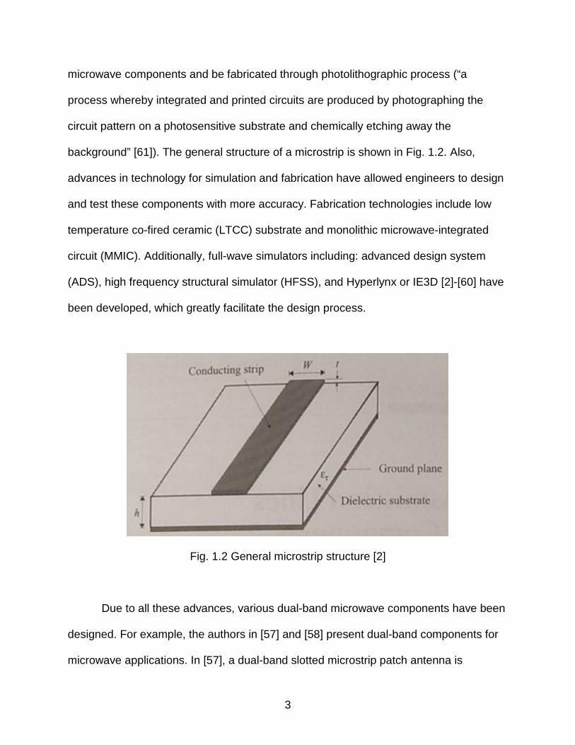
background” [61]). The general structure of a microstrip is shown in Fig. 1.2. Also,
advances in technology for simulation and fabrication have allowed engineers to design
and test these components with more accuracy. Fabrication technologies include low
temperature co-fired ceramic (LTCC) substrate and monolithic microwave-integrated
circuit (MMIC). Additionally, full-wave simulators including: advanced design system
(ADS), high frequency structural simulator (HFSS), and Hyperlynx or IE3D [2]-[60] have
been developed, which greatly facilitate the design process.
Fig. 1.2 General microstrip structure [2]
Due to all these advances, various dual-band microwave components have been
designed. For example, the authors in [57] and [58] present dual-band components for
microwave applications. In [57], a dual-band slotted microstrip patch antenna is
3
designed and shown with advantages of small size, low cost, and low weight for X-
band, Ku-band, and Radar microwave communications. The authors in [58] present the
use of composite right/left handed (CRLH) transmission lines based on complementary
split ring resonators (CSRRs) for dual-band microwave components. In their work, they
implement CRLH artificial lines instead of conventional impedance inverters to reduce
the size of the design to avoid the use of extra lump components. However, a major
drawback is the limitation in the arbitrariness of desired frequencies, which is one of the
motivations of this thesis.
1.3 An Introduction to Filters
Filters are crucial components in many microwave devices. Filters can select,
eliminate, or allow the transmission of selected signals to pass in any electronic device
[1], [2]. There are various types, functions, and responses of filters. Some types of filters
can be designed with lumped-elements, planar (i.e. microstrip, coplanar, or stripline),
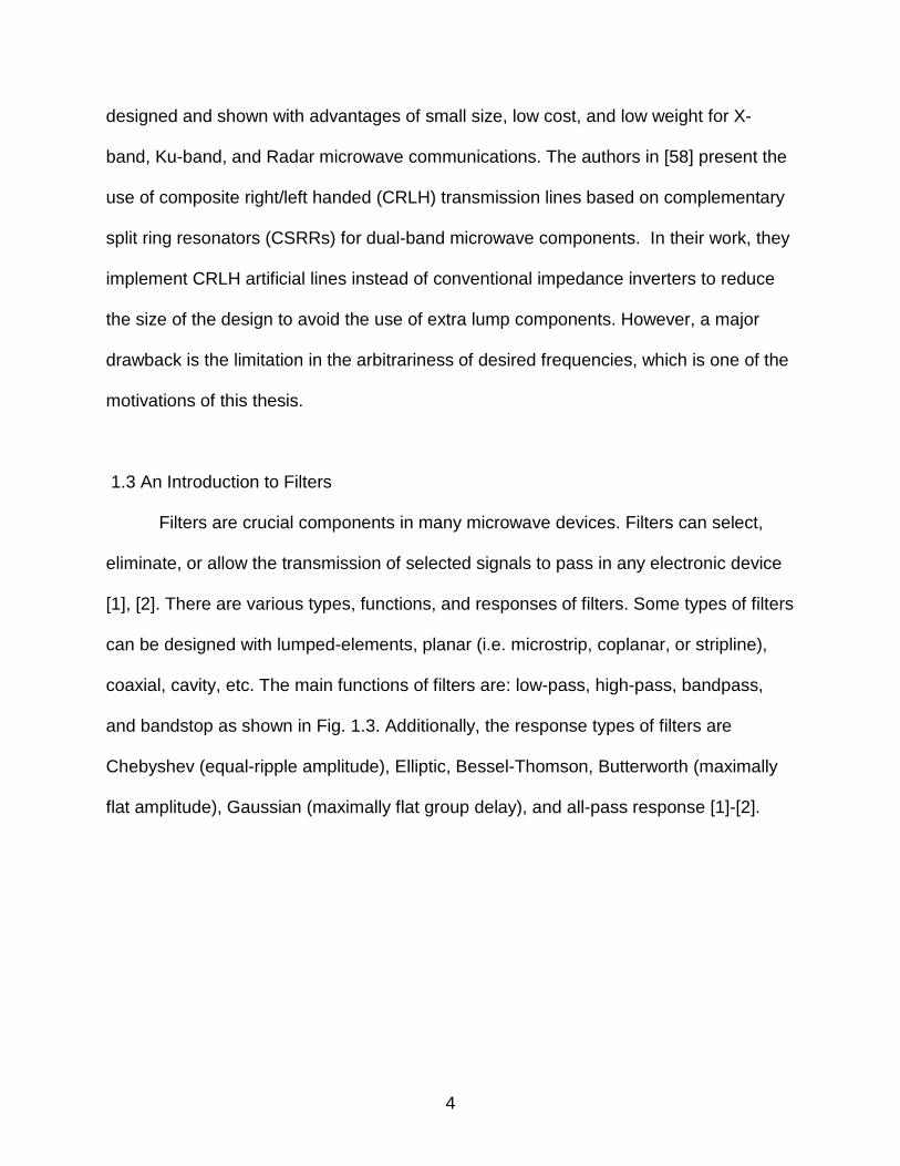
coaxial, cavity, etc. The main functions of filters are: low-pass, high-pass, bandpass,
and bandstop as shown in Fig. 1.3. Additionally, the response types of filters are
Chebyshev (equal-ripple amplitude), Elliptic, Bessel-Thomson, Butterworth (maximally
flat amplitude), Gaussian (maximally flat group delay), and all-pass response [1]-[2].
4
Fig. 1.3 Transfer functions of different types of filters [50]
Currently, to design filters, many engineers use lumped-components (resistor,
capacitors, and inductors) or resonators schemes such as T-shape, stepped-
impedance, coupled, etc. [1]-[36].
1.4 An Introduction to Baluns
Balun is a contraction of balanced to unbalanced. By definition, a balun
transforms unbalanced input signals to balanced output signals or vice versa [1], [36-
56]. There are many types of baluns and they are designed according to various needs
such as: the operating frequency, bandwidth, etc. It is further discussed in chapter 3. In
Fig. 1.4, two types of baluns are shown. Fig. 1.4(a) displays a transformer balun and it
can be used for low frequency operations. In addition, there are other microwave
component designs which can be used as baluns including 180o hybrid couplers [1], ring
5
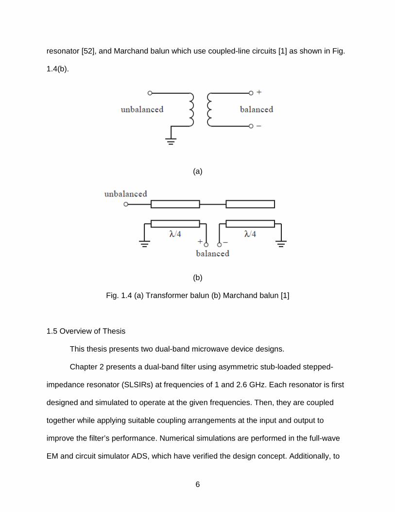
resonator [52], and Marchand balun which use coupled-line circuits [1] as shown in Fig.
1.4(b).
(a)
(b)
Fig. 1.4 (a) Transformer balun (b) Marchand balun [1]
1.5 Overview of Thesis
This thesis presents two dual-band microwave device designs.
Chapter 2 presents a dual-band filter using asymmetric stub-loaded stepped-
impedance resonator (SLSIRs) at frequencies of 1 and 2.6 GHz. Each resonator is first
designed and simulated to operate at the given frequencies. Then, they are coupled
together while applying suitable coupling arrangements at the input and output to
improve the filter’s performance. Numerical simulations are performed in the full-wave
EM and circuit simulator ADS, which have verified the design concept. Additionally, to
6
verify the simulated performance, the proposed dual-band filter is fabricated on the FR4
Isola printed circuit board (PCB).
Then, a novel dual-band balun with flexible frequency ratios is discussed in
chapter 3. The designed 3-port balun is based on a 4-port structure with the 4th port
terminated as an open end. Being a 4-port symmetrical network, even-odd mode
analysis is used to analyze the balun’s performance. Based on the derived explicit
design equations, a balun is designed to operate at 1.1 and 2 GHz. Numerical
simulations show low reflection coefficient S11, equal magnitudes at output ports as well
as 180o phase difference at the outputs. To validate the theoretical and numerical
simulations, the proposed balun is fabricated on the FR4 Isola PCB and measurement
results match well with the design theory.
7
CHAPTER 2
A NOVEL DUAL-BAND BANDPASS FILTER USING ASYMMETRIC
STUB-LOADED STEPPED IMPEDANCE RESONATORS
2.1 Introduction
Due to the rapid growth and development in wireless and network
communications, bandpass filters have become vital components of this process.
Today, there is still much on-going research to develop smaller, cheaper, and lower loss
filters [1]-[36]. A trapezoidal shape patch resonator was designed in [9] to increase the
parameter control for a wider passband. There have been several approaches to realize
dual-band filters. In [12], the authors use a combination of two single-band filters, and
thus, increasing its size and cost. Also, the authors in [13] and [14] use T-shape
structures due to their dual-band resonance and a good technique to reduce the overall
size of the filter. However, to improve the selectivity of the bandpass and bandstop filter,
in [15], a dual-band filter is designed based on microstrip-defected ground structure
(DGS) resonator pairs. In addition to changing the design, the authors in [17], [19], and
[22] use structures such as coplanar, hybrid, or metamaterial to reduce the size, control
the passbands, and ease the process of designing circuits. Also, to increase the
bandwidth, a parallel doubly coupled dual-band bandpass filter is proposed in [18]. It is
shown that doubly coupled configuration can almost double the bandwidth of a
conventional parallel coupled filter. In addition, authors in [20]-[21], and [26] apply
different substrates such as liquid crystal polymer (LCP) to fully control the passband in
a single filter, low-temperature co-fired ceramic (LTCC) to produce more compact
designs unlike printed circuit boards (PCBs), and half-mode substrate integrated
8
waveguide (HMSIW) to significantly reduce the size and still maintain low loss
properties. Then, in [24], authors use net-type resonator to improve the selectivity in
passbands with wide stopband rejection. However, this type of design has a major
disadvantage in which, it cannot be used for dual-band cellphone or WLAN applications.
Furthermore, to obtain dual-band characteristics in a single filter, engineers use the
technique shown in [32]-[35] which is to produce a coupling matrix from the reflection
and transfer functions obtained in the polynomial form of dual-band response. Finally,
stepped-impedance resonators have been widely used recently for dual-band bandpass
filters as seen in [2], [4]-[8], [16], [27]-[28].
This chapter presents a novel bandpass filter using two asymmetric stub-loaded
stepped-impedance resonators to achieve dual-band operation. In addition, new
coupling arrangements are applied at the input and output ports to improve its
performance and reduce its size. The proposed resonator is analyzed theoretically and
simulated in advanced design system (ADS). The proposed filter is fabricated on the
FR4 Isola PCB. It is designed to work at 1 and 2.6 GHz.
2.2 Theoretical Analysis
Fig. 2.1 shows the schematic of proposed asymmetric stub-loaded stepped-
impedance resonator (SLSIR). It is composed of three open-ended transmission lines.
All involved transmission lines have different impedances and electrical lengths.
Specifically, the first transmission line (starting from the left) has an impedance of Z1
and an electrical length of θ1. The vertically loaded stub has an impedance of Z3 and an
9
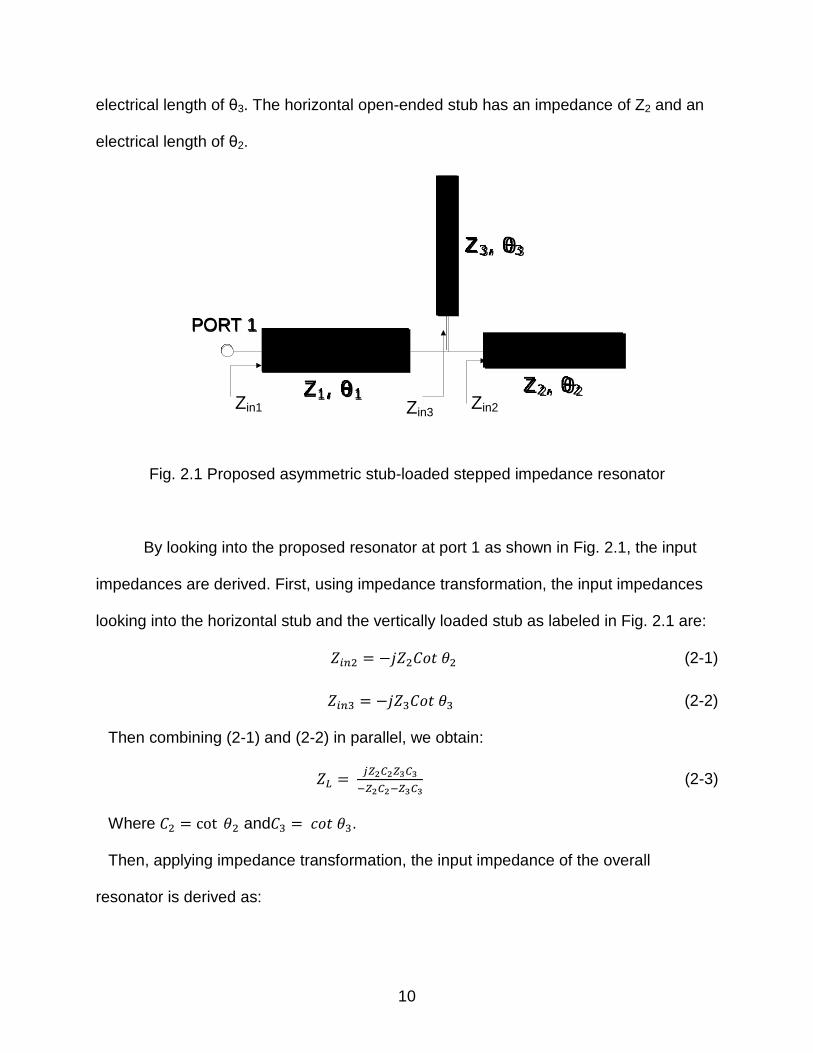
electrical length of θ3. The horizontal open-ended stub has an impedance of Z2 and an
electrical length of θ2.
Z1, θ1 Z2, θ2
Z3, θ3
PORT PORT 11
Zin1 Zin3 Zin2
Fig. 2.1 Proposed asymmetric stub-loaded stepped impedance resonator
By looking into the proposed resonator at port 1 as shown in Fig. 2.1, the input
impedances are derived. First, using impedance transformation, the input impedances
looking into the horizontal stub and the vertically loaded stub as labeled in Fig. 2.1 are:
𝑍𝑖𝑛2 = −𝑗𝑍2𝐶𝑜𝑡 𝜃2 (2-1)
𝑍𝑖𝑛3 = −𝑗𝑍3𝐶𝑜𝑡 𝜃3 (2-2)
Then combining (2-1) and (2-2) in parallel, we obtain:
𝑍𝐿 = 𝑗𝑍2𝐶2𝑍3𝐶3−𝑍2𝐶2−𝑍3𝐶3
(2-3)
Where 𝐶2 = cot 𝜃2 and𝐶3 = 𝑐𝑜𝑡 𝜃3.
Then, applying impedance transformation, the input impedance of the overall
resonator is derived as:
10
𝑍𝑖𝑛1 = 𝑗𝑍1𝑍2𝐶2𝑍3𝐶3−𝑗𝑍12𝑡1𝑍2𝐶2−𝑗𝑍12𝑡1𝑍3𝐶3−𝑍1𝑍2𝐶2−𝑍1𝑍3𝐶3−𝑍2𝐶2𝑍3𝐶3𝑡1
(2-4a)
When Zin1 = ∞ (resonant condition), we get the key design equation:
𝑍1𝑍2𝑡2
+ 𝑍1𝑍3𝑡3
+ 𝑍2𝑍3𝑡1𝑡2𝑡3
= 0 (2-4b)
Where 𝑡𝑖 = 𝑡𝑎𝑛𝜃𝑖 and𝐶𝑖 = 𝑐𝑜𝑡𝜃𝑖, 𝑖 = 1, 2, 3 …
For dual-band operation at frequencies 𝑓1 and𝑓2, the electrical lengths are derived as
follows:
𝜃1 = 𝑓1𝑓1+𝑓2
𝑛1𝜋@ 𝑓1 (2-5)
𝜃2 = 𝑓1
𝑓1+𝑓2𝑛2𝜋@ 𝑓1 (2-6)
𝜃3 = 𝑓1
𝑓1+𝑓2𝑛3𝜋@ 𝑓1 (2-7)
Where 𝑛1, 𝑛2, and𝑛3 = 1, 2, 3 … 6. For a more compact design while maintaining good
performance, 𝑛 = 1 and/or 2 are applied to yield the best results.
The impedances and electrical lengths of the proposed resonator are calculated
by applying equations (2-4b) and (2-5) - (2-7). Moreover, for easier implementation
using microstrip lines on conventional printed circuit boards (PCB), stub impedances
within the proposed resonator are selected to be between 20 and 120 Ω. Also, by
varying the stub impedances as well as 𝑛, the frequency ratio range (the ratio between
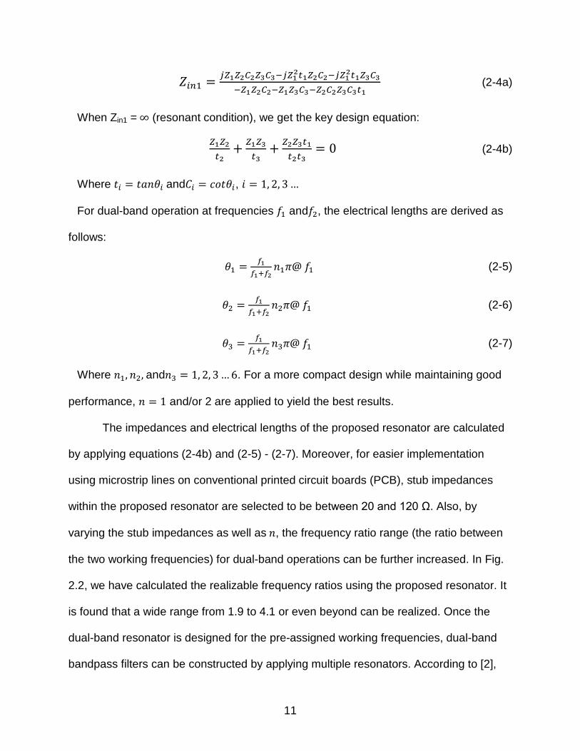
the two working frequencies) for dual-band operations can be further increased. In Fig.
2.2, we have calculated the realizable frequency ratios using the proposed resonator. It
is found that a wide range from 1.9 to 4.1 or even beyond can be realized. Once the
dual-band resonator is designed for the pre-assigned working frequencies, dual-band
bandpass filters can be constructed by applying multiple resonators. According to [2],
11
the general formulation for the external quality factor (Qe), and the coupling coefficient
between adjacent resonators (Mi) are defined as:
𝑄𝑒𝑛 = 𝑔𝑛𝑔𝑛+1𝐹𝐵𝑊
(2-8)
𝑀𝑖,𝑖+1 = 𝐹𝐵𝑊�𝑔𝑖𝑔𝑖+1
(2-9)
(a)
(b)
Fig. 2.2 Computed stub impedances under different frequency ratios (a) For 𝑛1 = 𝑛2 =
1 and 𝑛3 = 2. (b) For 𝑛1 = 𝑛2 = 1 and 𝑛3 = 3.
12
2.3 Simulated and Experimental Results
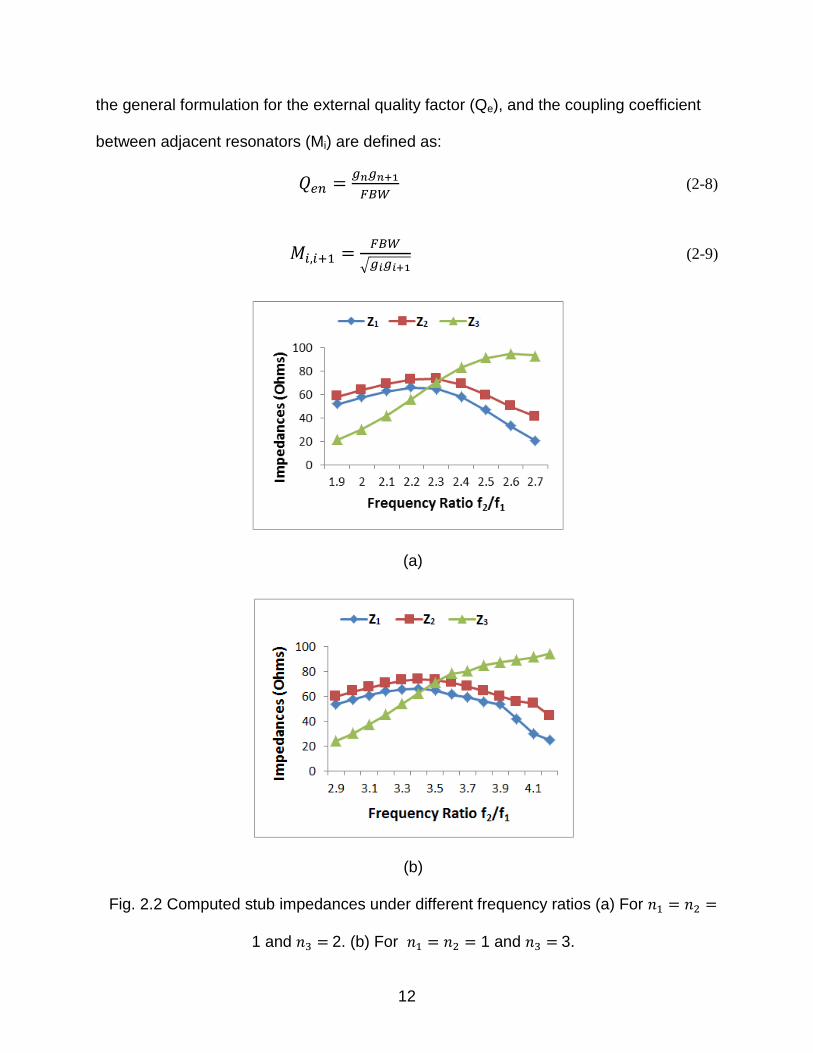
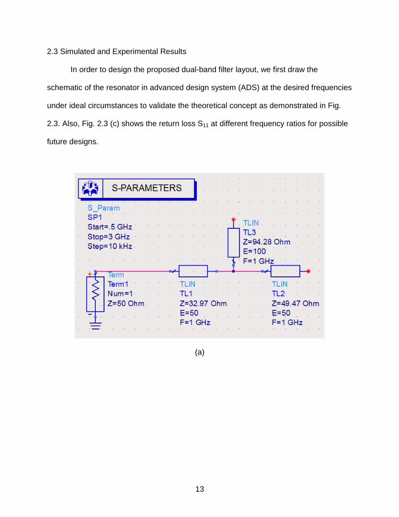
In order to design the proposed dual-band filter layout, we first draw the
schematic of the resonator in advanced design system (ADS) at the desired frequencies
under ideal circumstances to validate the theoretical concept as demonstrated in Fig.
2.3. Also, Fig. 2.3 (c) shows the return loss S11 at different frequency ratios for possible
future designs.
(a)
13
(b)
(c)
Fig. 2.3 (a) Schematic of proposed asymmetric resonator and (b) Simulation results
showing the resonant operating frequencies at 1 and 2.6 GHz (c) Return loss at
different frequency ratios (2.9 to 4.2 GHz)
14
Therefore, after the schematic simulations have met the theoretical work, a dual-
band filter is designed based on the proposed dual-band resonator. Fig. 2.4(a) shows
the layout of the proposed dual-band filter designed by (ADS) on a FR4 Isola printed
circuit board. The substrate used in this design has a dielectric constant εr = 3.67 and a
thickness h = 1.5mm. It is composed of two-stub-loaded resonators coupled together,
where “Si” represents the coupling gaps, i = 1, 2, 3...All the values of Si satisfy the
condition Si > 0.1 mm to avoid any fabrication problems.
50Ω
PORT1
PORT 2
50 ΩS3 S2S5
S1
S4
S6S7
S11
S8S9
S10L1, W1
L2, W2
L2, W2
L3, W3
L1, W1
L3, W3
(a)
15
(b)
(c)
Fig. 2.4 (a) Layout of proposed filter (b), (c) Simulation results of designed dual-band
bandpass filter showing insertion loss (S21), and return loss (S11) and phase response
16
The derived impedances and electrical lengths from (2-4b) are: Z1 = 32.97 Ω, Z2
= 49.47 Ω, Z3 = 94.28 Ω, θ1 = θ2 = 50o, and θ3 = 100o. While the calculated coupling
coefficient between resonators and the external quality factors at the input and output
given a fractional bandwidth of 10% are: M1,2 = 0.138, Qe1 = 5.24 and Qe2 = 8.43. Based
on these design parameters, the dimensions (unit: mm) for the designed filter are: S1 =
0.125, S2 = 0.143, S3 = 0.19, S4 = 0.124, S5 = 0.193, S6 = 0.148, S7 = 0.179, S8 = 0.106,
S9 = 0.13, S10 = 0.176, and S11 = 0.133. For the resonator, the dimensions (unit: mm)
are: L1 = 23.92, W1 = 6.06, L2 = 24.4, W2 = 3.3, L3 = 51.29 and W3 = 0.94.
(a)
17
(b)
(c)
Fig. 2.5 (a) Fabricated proposed filter (b), (c) Measured results of fabricated dual-band
filter showing return loss (S11) and phase response at proposed frequencies.
18
The designed filter’s performance is verified by numerical simulations (using the
full-wave electromagnetic simulator Momentum available in ADS). During the
simulations, frequency shifts occurred for certain frequency ratios (e.g. different
combinations of 𝑓1 and𝑓2). At lower frequency ratios, both 𝑓1 and 𝑓2shift down, while at
some higher frequency ratios, 𝑓1 shifts up, and 𝑓2shifts down. By adjusting the lengths of
the loaded stubs, we can control the frequencies, and avoid any major frequency
shifting due to the asymmetric resonator structures. Then in Fig. 2.4(b), (c), the
simulation results are shown. The working frequencies of the designed filter are at 0.99
and 2.59 GHz as wanted. Fig. 2.4(b) shows that return losses are smaller than -10 dB to
satisfy filter requirements. It also shows good insertion losses of less than 2 dB for
signal transmission. At 1 GHz, S21 = -0.438 dB and at 2.6 GHz, S21 = -1.168 dB. In Fig.
2.4(c) the phase response is illustrated in relation to the insertion loss (S21). Finally, in
Fig. 2.5 (a), the fabricated dual-band bandpass filter is shown. Fig. 2.5 (b) shows the
return loss at frequencies of: 0.95 and 2.509 GHz. It shows a slight shift in frequencies
possibly due to the PCB fabrication process. Then, in Fig. 2.5 (c), the measured phase
is presented.
2.4. Conclusion
In this chapter, we analyzed, designed, and simulated a novel dual-band
bandpass filter operating at 1 and 2.6 GHz using asymmetric SLSIRs. By using
impedance transformation, analytical design equations were derived. A second-order
bandpass filter employing proposed resonators is realized where specific coupling
19

arrangements are applied. Overall, the simulation results are in agreement with the
proposed design and theoretical work.
20
CHAPTER 3
A NOVEL DUAL-BAND BALUN DESIGN WITH FLEXIBLE FREQUENCY RATIOS
3.1 Introduction
As mentioned previously, the continuous development and growth in wireless
and network communications have caused a demand for dual-band and multiband
components which can reduce the system’s cost and size, and are attractive for
practical applications [1]-[60].
Baluns have become very useful and needed in various applications such as,
balanced mixers, push-pull amplifiers, frequency multiplier, 180o hybrid coupler, dipole
antennas, etc. [36]-[57]. There have been several approaches to design baluns. For
example, baluns [36], [47], [51], and [54] (e.g. Marchand baluns) can be made from
lumped or distributed components like transmission lines and coupled lines. According
to the analysis in [36], the use of optimal capacitor placement aids in the reduction of
the overall balun size but reduces the bandwidth by 20% to 40%. The authors in [37]
use two open stubs along the left and right branches which decrease the length of the
vertical branches by half and reducing the overall size of the balun. Additionally, the use
of tapped stubs is used to realize dual-band operation under even-odd mode excitations
and these stubs can be adjusted to achieve desired equal amplitude and 180o phase
difference at chosen frequencies [39]-[40]. In [41], the authors use partially coupled
stepped-impedance coupled-line resonators which have many advantages including
large dual-band frequency ratios, multiple coupling choices for easier fabrications, and
simple formulas to control coupling gaps. In [42], dual-band baluns are designed to
decrease the influence of RF feed cables in small antenna measurements. According to
21
[43], the use of lumped components shows poor phase differences and magnitude
response. The authors in [43] present a wideband balun using parallel strips offering
easy implementation not only for baluns, but also for other microwave components with
wide bandwidth. It is also shown that the proposed balun in [46] can be fabricated using
planar transmission lines with advantages such as light weight and compact size.
Additionally, baluns may be used for other microwave component applications such as:
ultra wide band (UWB) and ultra-high frequency (UHF) coupler for GIS PD detection
and dipoles as mentioned in [48], [50], and [53]. In [49], the authors present an analysis
of differential balun circuits based on the principle of transformers. According to [56] a
compact and broad-band three dimensional MMIC (monolithic microwave integrated
circuits) balun is presented. Finally, the balun designs presented in [54]-[55] are
fabricated using LTCC technology due to its high performance, integration density, and
reliability in the design of passive and active microwave components. In this chapter, we
present a novel dual-band balun with a simple and flexible structure. The proposed
balun is analyzed theoretically and simulated in advanced design system (ADS). An
experimental prototype of proposed balun is designed on FR4 Isola printed circuit board
(PCB), which works at 1.1 and 2 GHz.
3.2 Theoretical Analysis of Dual-Band Balun
Fig.3.1 shows the topology and physical layout of the proposed generalized
balun. It is composed of different transmission lines and a shunted stub along the center
of the left branch. All the involved transmission lines have different impedances (Z1, Z2,
and Z3) and electrical lengths (θ1, θ2, and θ3) respectively. In addition, an additional
22
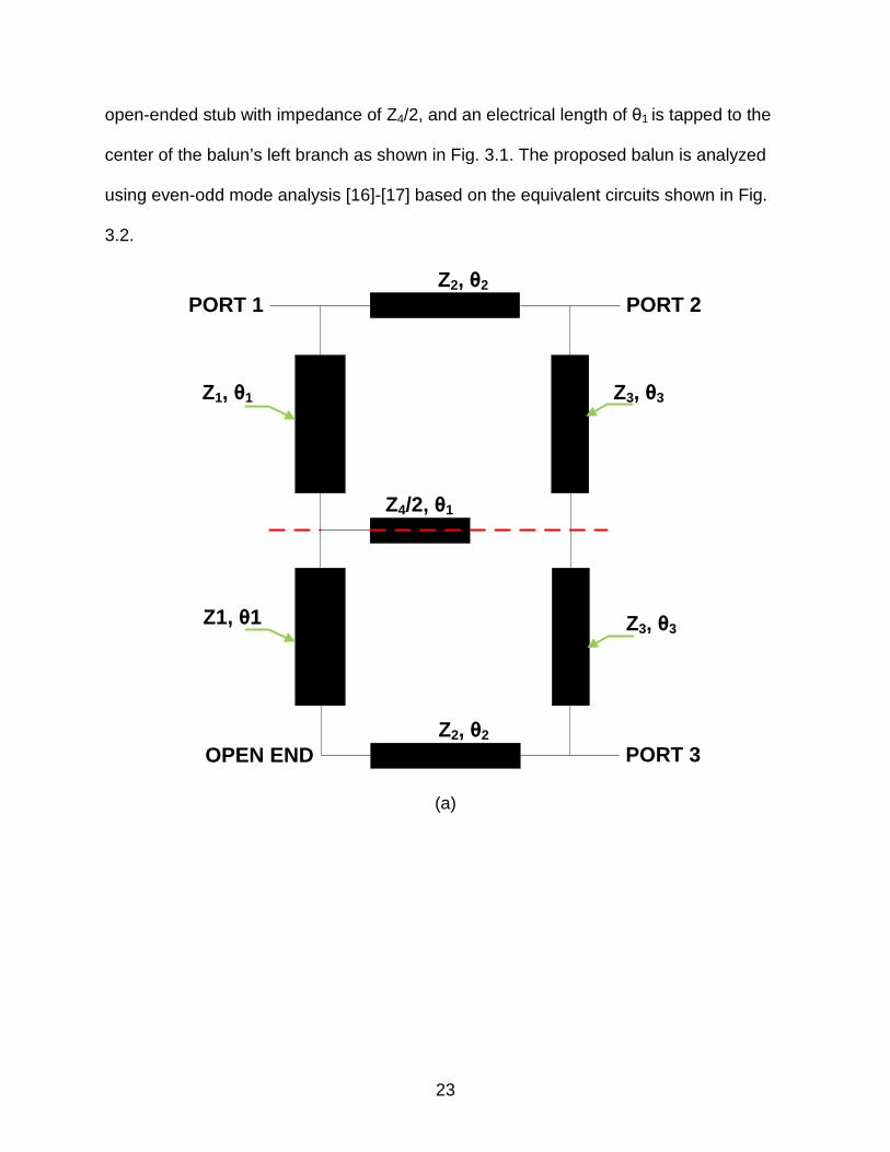
open-ended stub with impedance of Z4/2, and an electrical length of θ1 is tapped to the
center of the balun’s left branch as shown in Fig. 3.1. The proposed balun is analyzed
using even-odd mode analysis [16]-[17] based on the equivalent circuits shown in Fig.
3.2.
Z1, θ1
Z1, θ1
Z2, θ2
Z3, θ3
Z4/2, θ1
PORT 1 PORT 2
PORT 3OPEN END
Z3, θ3
Z2, θ2
(a)
23
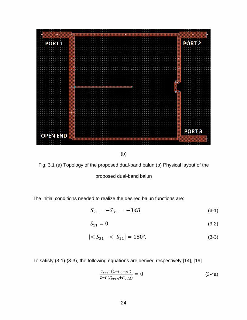
(b)
Fig. 3.1 (a) Topology of the proposed dual-band balun (b) Physical layout of the
proposed dual-band balun
The initial conditions needed to realize the desired balun functions are:
𝑆21 = −𝑆31 = −3𝑑𝐵 (3-1)
𝑆11 = 0 (3-2)
|< 𝑆31− < 𝑆21| = 180°. (3-3)
To satisfy (3-1)-(3-3), the following equations are derived respectively [14], [19]
𝑇𝑒𝑣𝑒𝑛(1−𝛤𝑜𝑑𝑑𝛤)2−𝛤(𝛤𝑒𝑣𝑒𝑛+𝛤𝑜𝑑𝑑)
= 0 (3-4a)
24
𝛤𝑒𝑣𝑒𝑛+𝛤𝑜𝑑𝑑−2𝛤𝑒𝑣𝑒𝑛𝛤𝑜𝑑𝑑𝛤2−𝛤(𝛤𝑒𝑣𝑒𝑛+𝛤𝑜𝑑𝑑)
= 0 (3-4b)
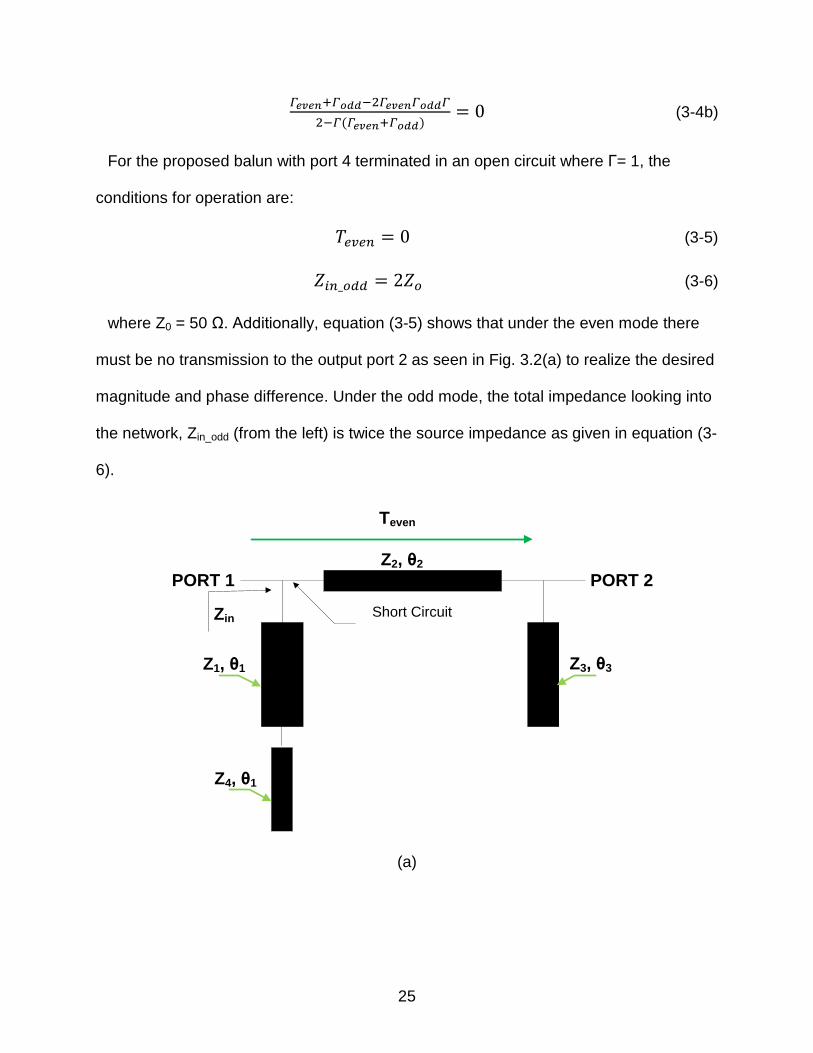
For the proposed balun with port 4 terminated in an open circuit where Γ= 1, the
conditions for operation are:
𝑇𝑒𝑣𝑒𝑛 = 0 (3-5)
𝑍𝑖𝑛_𝑜𝑑𝑑 = 2𝑍𝑜 (3-6)
where Z0 = 50 Ω. Additionally, equation (3-5) shows that under the even mode there
must be no transmission to the output port 2 as seen in Fig. 3.2(a) to realize the desired
magnitude and phase difference. Under the odd mode, the total impedance looking into
the network, Zin_odd (from the left) is twice the source impedance as given in equation (3-
6).
Z1, θ1
Z2, θ2
Z3, θ3
Z4, θ1
PORT 1 PORT 2
Zin
Teven
Short Circuit
(a)
25
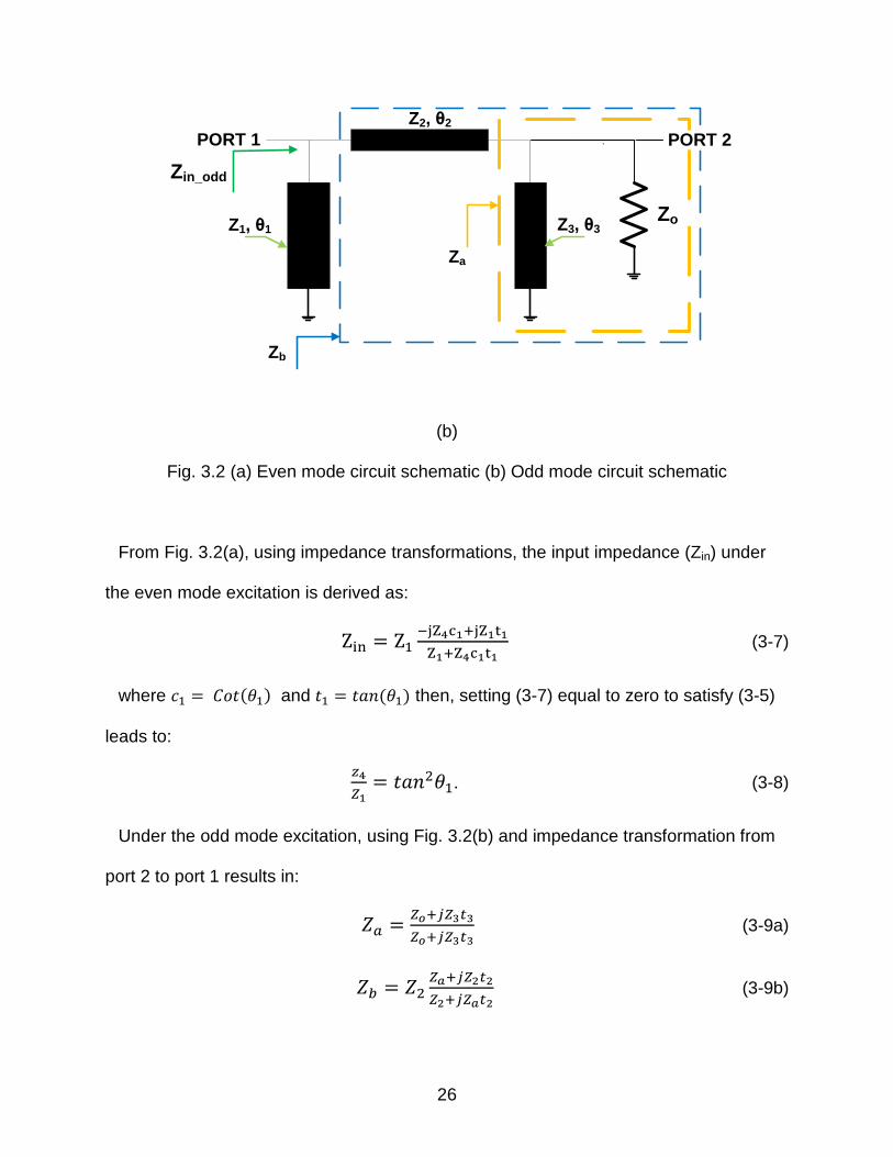
Z1, θ1
Z2, θ2
Z3, θ3
PORT 1 PORT 2
Zin_odd
`
Zo
Za
Zb
(b)
Fig. 3.2 (a) Even mode circuit schematic (b) Odd mode circuit schematic
From Fig. 3.2(a), using impedance transformations, the input impedance (Zin) under
the even mode excitation is derived as:
Zin = Z1−jZ4c1+jZ1t1Z1+Z4c1t1
(3-7)
where 𝑐1 = 𝐶𝑜𝑡(𝜃1) and 𝑡1 = 𝑡𝑎𝑛(𝜃1) then, setting (3-7) equal to zero to satisfy (3-5)
leads to:
𝑧4𝑍1
= 𝑡𝑎𝑛2𝜃1. (3-8)
Under the odd mode excitation, using Fig. 3.2(b) and impedance transformation from
port 2 to port 1 results in:
𝑍𝑎 = 𝑍𝑜+𝑗𝑍3𝑡3𝑍𝑜+𝑗𝑍3𝑡3
(3-9a)
𝑍𝑏 = 𝑍2𝑍𝑎+𝑗𝑍2𝑡2𝑍2+𝑗𝑍𝑎𝑡2
(3-9b)
26
𝑍𝑖𝑛_𝑜𝑑𝑑 = 𝑍𝑏(𝑗𝑍1𝑡1)𝑍𝑏+𝑗𝑍1𝑡1
(3-9c)
where Zo = 50 Ω, 𝑡𝑖 = 𝑡𝑎𝑛(𝜃𝑖), 𝑖 = 1, 2, 3 …
By substituting (3-9a) into (3-9b) and then (3-9c), Zin_odd is derived. Finally, to satisfy
(3-6), Zin_odd is set equal to 2Z0 which results in the following two equations:
𝑅𝑒[𝑍𝑖𝑛_𝑜𝑑𝑑] = 2𝑍𝑜 (3-10a)
𝐼𝑚[𝑍𝑖𝑛_𝑜𝑑𝑑] = 0 (3-10b)
For the proposed dual-band operation at frequencies 𝑓1 and 𝑓2, the electrical lengths
are derived as follows:
𝜃1 = 𝑓1𝑓1+𝑓2
𝑛1𝜋@ 𝑓1 (3-11)
𝜃2 = 𝑓1𝑓1+𝑓2
𝑛2𝜋@ 𝑓1 (3-12)
𝜃3 = 𝑓1𝑓1+𝑓2
𝑛3𝜋@ 𝑓1 (3-13)
where 𝑛1, 𝑛2, and𝑛3 = 1, 2, 3 … 6. For a more compact design while maintaining good
performance, n = 1 and/or 2 are applied to yield the best results.
By solving equations (3-10a) and (3-10b), the impedances and electrical lengths
of the proposed dual-band balun can be calculated. Then, using ADS, convert the
impedances and electrical lengths into physical values to design the proposed balun. A
very important factor for dual-band devices is the realizable frequency ratio (ratio
between the two working frequencies). The corresponding frequency ratio of proposed
balun has been calculated and the results are given in Fig. 3.3. For the easy
implementation using microstrip lines on conventional PCBs, impedances within the
proposed balun are selected to be between 18 and 120 Ω. From Fig. 3.3, it is shown
27
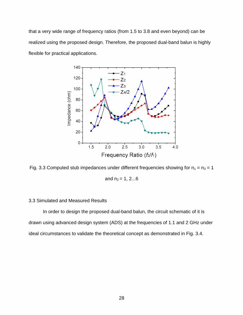
that a very wide range of frequency ratios (from 1.5 to 3.8 and even beyond) can be
realized using the proposed design. Therefore, the proposed dual-band balun is highly
flexible for practical applications.
Fig. 3.3 Computed stub impedances under different frequencies showing for n1 = n3 = 1
and n2 = 1, 2...6
3.3 Simulated and Measured Results
In order to design the proposed dual-band balun, the circuit schematic of it is
drawn using advanced design system (ADS) at the frequencies of 1.1 and 2 GHz under
ideal circumstances to validate the theoretical concept as demonstrated in Fig. 3.4.
28
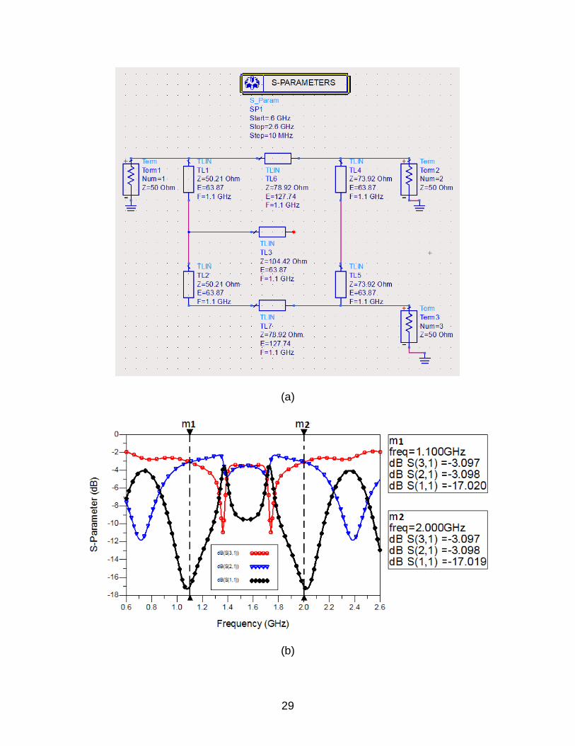
(a)
(b)
29
(c)
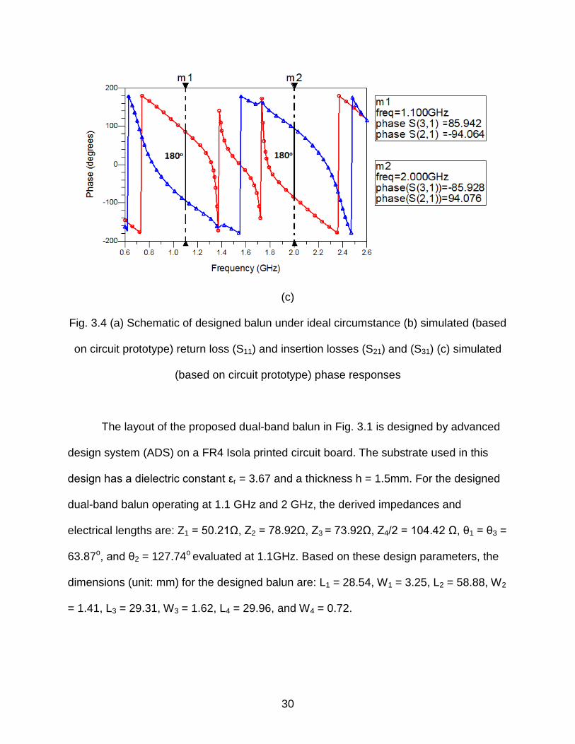
Fig. 3.4 (a) Schematic of designed balun under ideal circumstance (b) simulated (based
on circuit prototype) return loss (S11) and insertion losses (S21) and (S31) (c) simulated
(based on circuit prototype) phase responses
The layout of the proposed dual-band balun in Fig. 3.1 is designed by advanced
design system (ADS) on a FR4 Isola printed circuit board. The substrate used in this
design has a dielectric constant εr = 3.67 and a thickness h = 1.5mm. For the designed
dual-band balun operating at 1.1 GHz and 2 GHz, the derived impedances and
electrical lengths are: Z1 = 50.21Ω, Z2 = 78.92Ω, Z3 = 73.92Ω, Z4/2 = 104.42 Ω, θ1 = θ3 =
63.87o, and θ2 = 127.74o evaluated at 1.1GHz. Based on these design parameters, the
dimensions (unit: mm) for the designed balun are: L1 = 28.54, W1 = 3.25, L2 = 58.88, W2
= 1.41, L3 = 29.31, W3 = 1.62, L4 = 29.96, and W4 = 0.72.
30
(a)
(b)
31
(c)
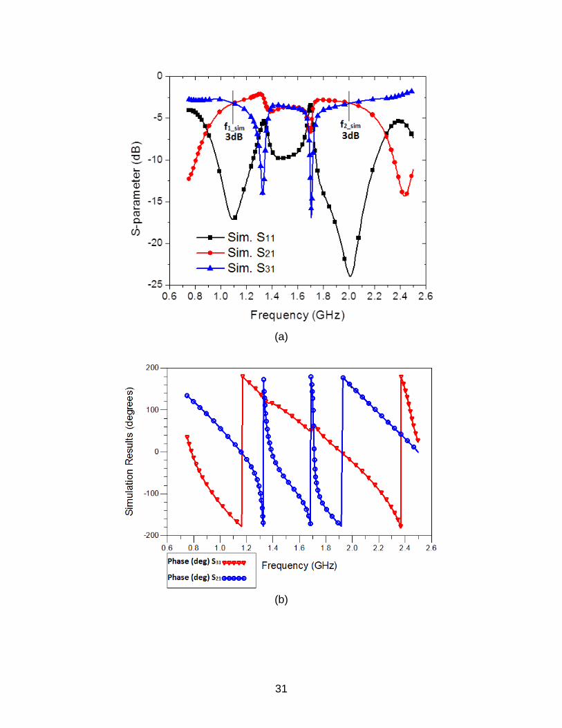
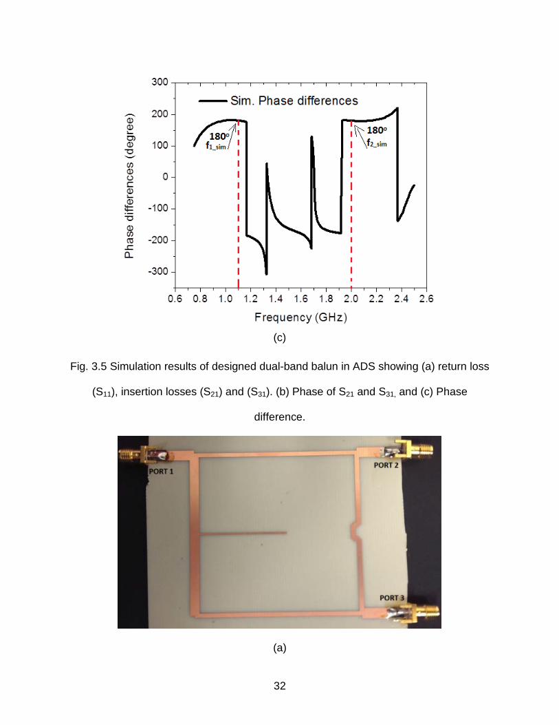
Fig. 3.5 Simulation results of designed dual-band balun in ADS showing (a) return loss
(S11), insertion losses (S21) and (S31). (b) Phase of S21 and S31, and (c) Phase
difference.
(a)
32
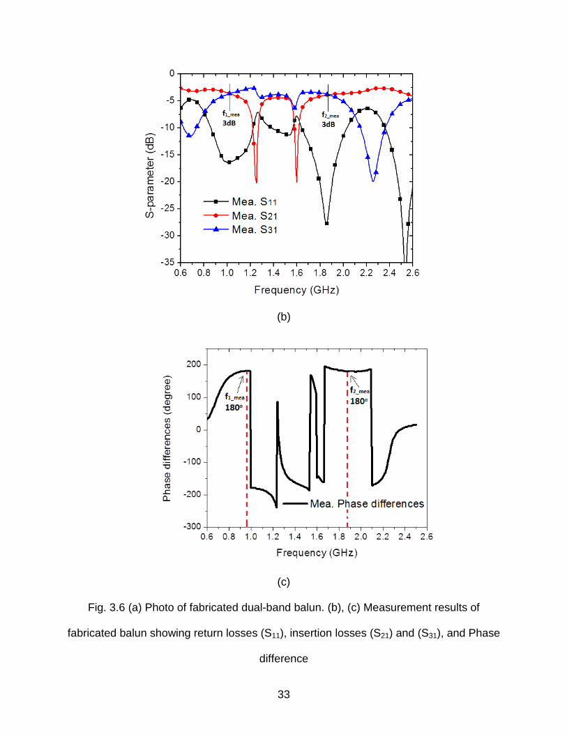
(b)
(c)
Fig. 3.6 (a) Photo of fabricated dual-band balun. (b), (c) Measurement results of
fabricated balun showing return losses (S11), insertion losses (S21) and (S31), and Phase
difference
33
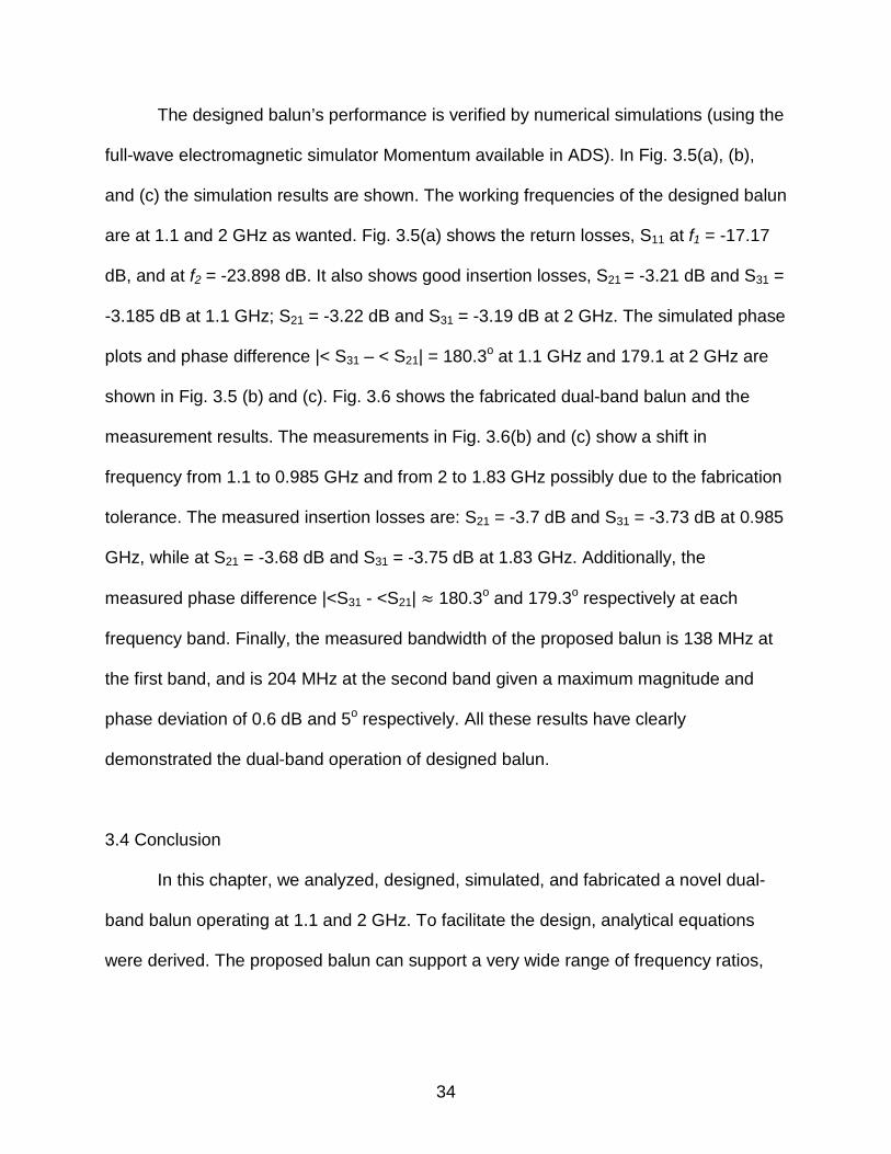
The designed balun’s performance is verified by numerical simulations (using the
full-wave electromagnetic simulator Momentum available in ADS). In Fig. 3.5(a), (b),
and (c) the simulation results are shown. The working frequencies of the designed balun
are at 1.1 and 2 GHz as wanted. Fig. 3.5(a) shows the return losses, S11 at f1 = -17.17
dB, and at f2 = -23.898 dB. It also shows good insertion losses, S21 = -3.21 dB and S31 =
-3.185 dB at 1.1 GHz; S21 = -3.22 dB and S31 = -3.19 dB at 2 GHz. The simulated phase
plots and phase difference |< S31 – < S21| = 180.3o at 1.1 GHz and 179.1 at 2 GHz are
shown in Fig. 3.5 (b) and (c). Fig. 3.6 shows the fabricated dual-band balun and the
measurement results. The measurements in Fig. 3.6(b) and (c) show a shift in
frequency from 1.1 to 0.985 GHz and from 2 to 1.83 GHz possibly due to the fabrication
tolerance. The measured insertion losses are: S21 = -3.7 dB and S31 = -3.73 dB at 0.985
GHz, while at S21 = -3.68 dB and S31 = -3.75 dB at 1.83 GHz. Additionally, the
measured phase difference |<S31 - <S21| ≈ 180.3o and 179.3o respectively at each
frequency band. Finally, the measured bandwidth of the proposed balun is 138 MHz at
the first band, and is 204 MHz at the second band given a maximum magnitude and
phase deviation of 0.6 dB and 5o respectively. All these results have clearly
demonstrated the dual-band operation of designed balun.
3.4 Conclusion
In this chapter, we analyzed, designed, simulated, and fabricated a novel dual-
band balun operating at 1.1 and 2 GHz. To facilitate the design, analytical equations
were derived. The proposed balun can support a very wide range of frequency ratios,
34

which is highly favorable for practical applications. The simulation and experimental
results are in agreement with the design theory.
35
CHAPTER 4
CONCLUSION AND FUTURE WORKS
4.1 Conclusion
In this thesis, a brief introduction into microwave engineering and the need of
dual-band and multiband microwave components is introduced. Also, there is an
introduction to dual-band components, microwave filters, and baluns. Next, as the focus
of this thesis, two dual-band microwave designs have been presented for wireless and
communication systems. In chapter 2, a novel dual-band bandpass filter using
asymmetric stub-loaded stepped-impedance resonators designed to operate at 1 and
2.6 GHz was analyzed, designed, simulated, and fabricated in the Isola printed circuit
board (PCB). Then in chapter 3, a dual-band balun with flexible frequency ratios is
presented. We have also presented a prototype balun operating at 1.1 and 2 GHz,
which was analyzed theoretically, simulated, and fabricated in the Isola (PCB) featuring
compact size, good performance, and light weight. The two proposed microwave
designs and their flexible dual-band frequency operations are important for many
microwave and RF applications.
4.2 Future Work
In order to develop smaller, more compact, higher performance, and broader
bandwidth microwave devices, there is the need to continue investigating and designing
new dual-band and multi-band prototypes to meet the current demands of wireless
systems. Future work may also include the fabrication of current designs under new
substrates and testing for functionality. Also, as demonstrated in Fig. 2.3 (c), it is
36

possible to design dual-band bandpass resonators at higher frequency ratios for future
designs.
37
REFERENCES
[1] D. M. Pozar, Microwave Engineering, 4nd ed. New Jersey: Wiley, 2012.
[2] Jia-Sheng Hong, Microstrip filters for RF/Microwave applications, 2nd ed. New
Jersey: Wiley, 2011.
[3] H. Zhang and K. J. Chen, “A stub tapped branch-line coupler for dual-band
operations,” IEEE Microw. Wireless Compon. Lett., vol. 17, no. 2, pp. 106-108, Feb.
2007.
[4] Y. P. Zhang and M. Sun, “Dual-band microstrip bandpass filter using stepped-
impedance resonators with new coupling schemes,” IEEE Trans. Microw. Theory
Tech., vol. 54, no. 10, pp. 3779-3785, Oct. 2006.
[5] S. R. Wu, K. W. Hsu, and W. H. Tu, “Compact wide-stopband microstrip bandpass
filter based on stub-loaded stepped impedance resonators,” IET Microw. Antennas
Propag., vol. 6, no. 13, pp. 1422-1428, 2012.
[6] X. Guan, F. Wen, C. Wang, S. Jiang, and H. Liu, “A cross-shaped stepped-
impedance resonator bandpass filter with wide stopband,” ICMMT Microw.
Milli.Wave Tech., pp. 574-576, May. 2010.
[7] S. Zhang and L. Zhu, “Synthesis design of dual-band bandpass filters with λ/4
stepped-impedance resonators,” IEEE Trans. Microw. Theory Tech., vol. 61, no. 5,
pp. 1812-1819, May. 2013.
[8] J. Lim, M. Nam, H. Choi, and J. Lee, “Two-port balanced dual-band bandpass filter
based on stepped impedance resonators,” PACM Proced. Asia-Pacific Microw.
Conf., pp. 1114-1117, Dec. 2010.
38
[9] J. K. Xiao, Q. X. Chu, and Y. Wang, “New patch resonator bandpass filter with
wideband and tunable operation,” APMC Microw. Confer. Asia-Pacific., pp. 1-3, Dec.
2008.
[10] J.R. Lee, J. H. Cho, and S. W. Yun, “New compact bandpass filter using
microstrip λ/4 resonators with open stub inverter,” IEEE Microw. Guided Wave Lett.,
vol. 10, no. 12, pp. 526-527, Dec. 2000
[11] X. Y. Zhang, J. X. Chen, and Q. Xue, “Dual-band bandpass filters using stub-
loaded resonators,” IEEE Microw. Wireless Compon. Lett., vol. 17, no. 8, pp. 583-
585, Aug. 2007.
[12] H. Miyake, S. Kitazawa, T. Yamada, and Y. Nagatomi, “A miniaturized monolithic
dual band filter using ceramic lamination technique for dual mode portable
telephones,” IEEE MTT-S Int., Microw. Symp. Dig., vol. 2, pp. 789-792, 1997.
[13] C. J. Chen, “Analytical Derivation of T-shaped structures for synthesis of quarter-
wavelength transmission lines,” IEEE Microw. Comp. Lett., vol. 23, no. 10, pp. 524-526,
Oct. 2013.
[14] K. Deng, Y. Xu, and W. Che, “A compact dual-band bandpass filter using
asymmetric T-shape resonators,” APMC Microw. Confer. Proced. Asia-Pacific, pp.
1139-1141, Dec. 2012.
[15] E. Corrales, O. Menendez, and P. de Paco, “Compact dual-band filter based on
microstrip-DGS resonator pairs,” EuMC Microw. Confer. European, pp.464-467, Oct.
2011.
39
[16] L. Gao, X. Y. Zhang, K. X. Wang, and B.-J. Hu, “Miniaturized dual-band
bandpass filter using quarter-wavelength stepped-impedance resonators,” APMC
Microw. Confer. Proced. Asia Pacific, pp. 238-240, Dec. 2012.
[17] H. Chen and Y.-X Zhang, “Design of a novel dual-band bandpass filter using
microstrip/CPW structure,” ICCCAS Conmm, Circuits and Syst., pp. 1216-1218, May
2008.
[18] C.-M. Rao, T.-J. Wong, and M.-H Ho, “A parallel doubly coupled dual-band
bandpass filter,” IEEE MTT-S Microw. Symp. Digest, pp. 511-514, June 2006.
[19] G.-S. and C. H. Chen, “Dual-band balun bandpass filter with hybrid structure,”
IEEE Microw. Wirel. Comp. Lett., vol. 21, iss. 7, pp. 356-358, July 2011.
[20] A. Bavisi, M. Swaminathan, and E. Mina, “Liquid crystal polymer-based planar
lumped component dual-band filters for dual-band WLAN systems,” IEEE Radio Wirel
Symp., pp. 538-542, Jan. 2007.
[21] S. Oshima, K. Wada, R. Murata, and Y. Shimakata, “Multilayer dual-band
bandpass filter in low temperature co-fired ceramic substrate for ultra-wideband
applications,” IEEE Trans. Microw. Theory. Techn., vol. 58, iss. 3, pp. 614-623, March
2010.
[22] G. Siso, J. Bonache, and F. Martin, “Miniaturization and dual-band operation in
planar microwave components by using resonant –type metamaterial transmission
lines,” IEEE MTT-S Art Min. RF Microw. Pass. Comp., pp. 34-37, Dec. 2008.
[23] Y. Liu, and W. Dou, “A dual-band filter realized by alternately connecting the
main transmission-line with shunt stubs and shunt serial resonators,” IEEE Microw.
Wirel. Comp. Lett., vol. 19, iss. 5, pp. 296-298, May 2009.
40
[24] C.-H. Tseng, and H.-Y. Shao, “A new dual-band microstrip bandpass filter using
net-type resonators,” IEEE Microw. Wirel. Comp. Lett., vol. 20, iss. 4, pp.196-198, April
2010.
[25] L.-C. Tsai and C.-W. Hsue, “Dual-band bandpass filters using equal-length
coupled-serial-shunted lines and z-transform technique,” IEEE Trans.Microw. Theory
Tech., vol. 52, iss. 4, pp. 1111-1117 April 2004.
[26] V. Sekar and K. Entesari, “A novel compact dual-band half-mode substrate
integrated waveguide bandpass filter,” IEEE MTT-S Microw. Symp. Digest, pp. 1-4,
June 2011.
[27] J. Konpang, “A dual-band filter using coupled-feed with asymmetrical stepped-
impedance resonator,” DICTAP Dig. Inf. Comm. Tech. App., pp. 333-337, May 2012.
[28] M. Mokhtaari, J. Bornemann, and S. Amari, “New reduced-size step-impedance
dual-band filters with enhanced bandwidth and stopband performance,” IEEE MTT-S
Microw. Symp. Digest, pp. 1181-1184, June 2006.
[29] S. Sun and L. Zhu, “Compact dual-band microstrip bandpass filter without
external feeds,” IEEE Microw. Wirel. Comp. Lett., vol. 15, iss. 10, pp. 644-646, Oct.
2005.
[30] D. E. Senior, X. Cheng, M. Machado, and Y.-K. Yoon, “Single and dual band
bandpass filters using complementary split ring resonator loaded half mode substrate
integrated waveguide,” IEEE APSURSI Ant. Prop. Soc. Int. Symp., pp. 1-4, July 2010.
[31] X. Y. Zhang, J.-X. Chen, Q. Xue, and S.-M. Li, “Dual-band bandpass filter using
stub-loaded resonators,” IEEE Microw. Wirel. Comp. Lett., vol. 17, no.8, pp. 583-585,
Aug. 2007.
41
[32] R. Cameron, M. Yu, and Y. Wang, “Direct-coupled microwave filters with single
and dual stopbands,” IEEE Trans. Microw, Theory and Techn., vol. 53, no.11, pp. 3288-
3297, 2005.
[33] S. Bila, R. Cameron, P, Lenoir, V. Lunot, and F. Seyfert, “Chebyshev synthesis
for multi-band microwave filters,” IEEE MTT-S International Microw. Symp. Digest, pp.
1221-1224, 2006.
[34] M. Mokhtaari, J. Bornemann, K. Rambabu, and S. Amari, “Coupling-matrix
design of dual and triple passband filters,” IEEE Trans. Microw. Theory Tech., vol.54,
no. 11, pp. 3940-3946, 2006.
[35] Y. Zhang, K. Zaki, J. Ruiz-Cruz, and A. Atia, “Analytical synthesis of generalized
multi-band microwave filters,” IEEE/MTT-S International Microw. Symp., pp. 1273-1276,
2007.
[36] K. S. Ang, Y. C. Leong, and C. H. Lee, “Analysis and design of miniaturized
lumped-distributed impedance-transforming baluns,” IEEE Trans. Microw. Theory
Tech., vol. 51, no. 3, pp. 1009-1017, March. 2003.
[37] M. J. Park and B. Lee, “Stubbed branch line balun,” IEEE Microw. Wireless
Compon. Lett., vol. 17, no. 3, pp. 166-171, March. 2007.
[38] Y. C. Leong, K. S. Ang, and C. H. Lee, “A derivation of a class of 3-port baluns
from symmetrical 4-port networks,” IEEE MTT-S Microw. Symp. Digest, vol. 2, pp.
1165-1168, June. 2002.
[39] H. Zhang, Y. Peng, and H. Xin, “A tapped stepped-impedance balun with dual-
band operations,” IEEE Antenn. Wireless Propag. Lett., vol. 7, pp. 119-122, 2008.
42
[40] H. Zhang, Y. Peng, and H. Xin, “Design of dual-band balun with tapped stubs,”
IEEE Radio Wireless Symp., pp. 859-862, Jan. 2008.
[41] X. Gao, L. K. Yeung, and K. L. Wu, “A dual-band balun using partially coupled
stepped-impedance coupled-line resonators,” IEEE Trans. Microw. Theory Tech.,
vol. 56, no. 6, pp. 1455-1460, June. 2008.
[42] C. Icheln and P. Vainikainen, “Dual-frequency balun to decrease influence of RF
feed cables in small antenna measurements,” Electron. Lett., vol. 36, iss. 21, pp.
1760-1761, Oct. 2000.
[43] J. Shao, R. Zhou, C. Chen, X. Wang, H. Kim, and H. Zhang, “Design of a
wideband balun using parallel strips,” IEEE Microw. Wireless Compon. Lett., vol. 23,
no. 3, pp. 125-127, March 2013.
[44] H. Zhang and H. Xin, “Dual-band branch-line balun for millimeter-wave
applications,” IEEE MTT-S International Microw. Symp. Digest,pp. 717-720, June
2009.
[45] H. Zhang and H. Xin, “Dual-band with fully matched performance,” APMC
Microw. Conf. pp.1-4, Dec. 2008.
[46] H. Zhang and H. Xin, “Stepped-impedance based dual-band and dual-function
balun for 20/44 GHz applications,” EuCAP Antennas Propag., pp.2595-2598, March,
2009.
[47] C. Y. Ng, M. Chongcheawchamnam, and I. D. Robertson, “Analysis and design
of a high performance planar marchand balun,” IEEE MTT-S International Microw,
Symp. Digest., vol. 1, pp. 113-116, June 2002.
43
[48] J.-G. Choi, S.-H. Yi, and K.-H. Kim, “Development of a novel tapered balun for
the UWB UHF coupler,” High-Volt. Workshop Power Modul. Symp., pp. 493-496,
May 2004.
[49] L. Sun, Y. Chen, K. Sun, and W. Wu, “ Analysis of differential balun circuits,”
ISSSE, Signals Syst. Electr., vol. 1, pp.1-4, Sept, 2010.
[50] Q.-Y. Zhang, Q.-X. Chu, and Y. Wang, “Compact printed dual-band dipole with
wideband integrated balun,” Electronic Lett., vol. 45, iss. 24, pp. 1209-1210, Nov.
2009.
[51] P. Aflaki, R. Negra, and F. M. Ghannouchi, “ Dual-band rat-race balun structure
using transmission-lines and lumped component resonators,” IEEE MTT-S
International MIcrow. Symp. Digest, pp. 1572-1575, May 2010.
[52] E.-Y. Jung and H.-Y. Hwang, “A balun-BPF using a dual mode ring resonator,”
IEEE Microw. Wirel. Comp. Lett., vol.17, no. 9, pp. 652-654, Sept, 2007.
[53] H. Zhang and H. Xin, ”A dual-band dipole antenna with integrated-balun,” IEEE
Trans. Anten.Propag., vol.57, no.3, pp. 786, 789, March 2009.
[54] Y. Dai, H. Yin, Y. Feng, P. Li, Q. Han, and M. Han, “A LTCC miniaturized
broadbrand modified marchand balun,” ISCIT Intern. Symp. Comm. Inform, pp. 110-
113, Oct. 2012.
[55] Y.-Xin Guo, Z. Y. Zhang, L. C. Ong, and M. Y. W. Chia, “A novel LTCC
miniaturized dualband balun,” IEEE Microw. Wirel. Comp. Lett., vol. 16, no. 3, pp.
143-145, March, 2006.
44
[56] K. Nishikawa, I. Toyoda, and T. Tokumitsu, “Compact and broad-band three-
dimensional MMIC balun,” IEEE Trans. Microw. Theory. Techn., vol. 47, no. 1, Jan.
1999.
[57] A. Das, B. Datta, S. Chatterjee, M. Mukherjee, and S. K. Chowdury, “Dual-band
slotted microstrip patch antenna design,” ICICES Inf. Comm. Embed. Syst., pp. 850-
855, Feb. 2013.
[58] J. Bonache, G. Siso, M. Gil, A. Iniesta, J. Garcia-Rincon, and F. Martin,
“Application of composite right/left handed (CRLH) transmission lines based on
complementary split ring resonators (CSRRs) to the design of dual-band microwave
components,” IEEE Microw. Wirel. Comp. Lett., vol. 18, no. 8, Aug. 2008.
[59] C. Caloz and T. Itoh, Electromagnetic Metamaterials: Transmission Line Theory
and Microwave Applications. New York: Wiley, 2006.
[60] F. Gustrau, “RF and Microwave Engineering: Fundamentals of Wireless
Communications,” Hoboken: Wiley, 2012. Ebook Library. Web. March 2014.
[61] Dictionary.com. “photolithography,” in Dictionary.com Unabridged. Source
location: Random House, Inc.
http://dictionary.reference.com/browse/photolithography. Available:
http://dictionary.reference.com/ Accessed: March 13, 2014.
45