DLPC6540 Display Controller datasheet (Rev. B) - Mouser ...
96
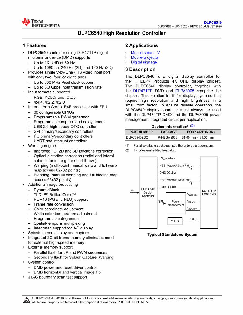
DLPC6540 High Resolution Controller 1 Features • DLPC6540 controller using DLP471TP digital micromirror device (DMD) supports – Up to 4K UHD at 60 Hz – Up to 1080p at 240 Hz (2D) and 120 Hz (3D) • Provides single V-by-One ® HS video input port with one, two, four, or eight lanes – Up to 600 MHz Pixel clock support – Up to 3.0 Gbps input transmission rate • Input formats supported – RGB, YCbCr and ICtCp – 4:4:4, 4:2:2, 4:2:0 • Internal Arm Cortex-R4F processor with FPU – 88 configurable GPIOs – Programmable PWM generator – Programmable capture and delay timers – USB 2.0 high-speed OTG controller – SPI primary/secondary controllers – I 2 C primary/secondary controllers – UART and interrupt controllers • Warping engine – Improved 1D, 2D and 3D keystone correction – Optical distortion correction (radial and lateral color distortion e.g. for short throw ) – Warping (multi-point manual warp and full warp map access 62x32 points) – Blending (manual blending and full bleding map access 63x32 points) • Additional image processing – DynamicBlack – TI DLP ® BrilliantColor™ – HDR10 (PQ and HLG) support – Frame rate conversion – Color coordinate adjustment – White color temperature adjustment – Programmable degamma – Spatial-temporal multiplexing – Integrated support for 3-D display • Splash screen display and capture • Integrated 2G-bit frame memory eliminates need for external high-speed memory • External memory support – Parallel flash for µP and PWM sequences – Secondary flash for Splash Capture, Warping • System control – DMD power and reset driver control – DMD horizontal and vertical image flip • JTAG boundary scan test support 2 Applications • Mobile smart TV • Mobile projector • Digital signage 3 Description The DLPC6540 is a digital display controller for the TI DLP ® Products 4K UHD display chipset. The DLPC6540 display controller, together with the DLP471TP DMD and DLPA3005 comprise the chipset. This solution is fit for display systems that require high resolution and high brightness in a small form factor. To ensure reliable operation, the DLPC6540 display controller must always be used with the DLP471TP DMD and the DLPA3005 power management integrated circuit per application. Device Information (1)(2) PART NUMBER PACKAGE BODY SIZE (NOM) DLPC6540ZDC P-HBGA (676) 31.00 mm × 31.00 mm (1) For all available packages, see the orderable addendum. (2) Includes embedded heat slug. 1.8 V V BIAS V RESET LS_Interface DMD DCLKA V OFFSET Vx1 HSSI Macro A Data Pair 8 DLPC6540 Display Controller SPI DMD DCLKB HSSI Macro B Data Pair 8 Power Management VREG DLP471TP HSSI DMD Typical Standalone System www.ti.com DLPC6540 DLPS168B – MAY 2020 – REVISED AUGUST 2020 Copyright © 2021 Texas Instruments Incorporated Submit Document Feedback 1 Product Folder Links: DLPC6540 DLPC6540 DLPS168B – MAY 2020 – REVISED AUGUST 2020 An IMPORTANT NOTICE at the end of this data sheet addresses availability, warranty, changes, use in safety-critical applications, intellectual property matters and other important disclaimers. PRODUCTION DATA.
-
Upload
khangminh22 -
Category
Documents
-
view
3 -
download
0
Transcript of DLPC6540 Display Controller datasheet (Rev. B) - Mouser ...
DLPC6540 High Resolution Controller
1 Features• DLPC6540 controller using DLP471TP digital
micromirror device (DMD) supports– Up to 4K UHD at 60 Hz– Up to 1080p at 240 Hz (2D) and 120 Hz (3D)
• Provides single V-by-One® HS video input portwith one, two, four, or eight lanes– Up to 600 MHz Pixel clock support– Up to 3.0 Gbps input transmission rate
• Input formats supported– RGB, YCbCr and ICtCp– 4:4:4, 4:2:2, 4:2:0
• Internal Arm Cortex-R4F processor with FPU– 88 configurable GPIOs– Programmable PWM generator– Programmable capture and delay timers– USB 2.0 high-speed OTG controller– SPI primary/secondary controllers– I2C primary/secondary controllers– UART and interrupt controllers
• Warping engine– Improved 1D, 2D and 3D keystone correction– Optical distortion correction (radial and lateral
color distortion e.g. for short throw )– Warping (multi-point manual warp and full warp
map access 62x32 points)– Blending (manual blending and full bleding map
access 63x32 points)• Additional image processing
– DynamicBlack– TI DLP® BrilliantColor™– HDR10 (PQ and HLG) support– Frame rate conversion– Color coordinate adjustment– White color temperature adjustment– Programmable degamma– Spatial-temporal multiplexing– Integrated support for 3-D display
• Splash screen display and capture• Integrated 2G-bit frame memory eliminates need
for external high-speed memory• External memory support
– Parallel flash for µP and PWM sequences– Secondary flash for Splash Capture, Warping
• System control– DMD power and reset driver control– DMD horizontal and vertical image flip
• JTAG boundary scan test support
2 Applications• Mobile smart TV• Mobile projector• Digital signage
3 DescriptionThe DLPC6540 is a digital display controller forthe TI DLP® Products 4K UHD display chipset.The DLPC6540 display controller, together withthe DLP471TP DMD and DLPA3005 comprise thechipset. This solution is fit for display systems thatrequire high resolution and high brightness in asmall form factor. To ensure reliable operation, theDLPC6540 display controller must always be usedwith the DLP471TP DMD and the DLPA3005 powermanagement integrated circuit per application.
Device Information(1)(2)
PART NUMBER PACKAGE BODY SIZE (NOM)DLPC6540ZDC P-HBGA (676) 31.00 mm × 31.00 mm
(1) For all available packages, see the orderable addendum.(2) Includes embedded heat slug.
1.8 V
VBIAS
VRESET
LS_Interface
DMD DCLKA
VOFFSET
Vx1
HSSI Macro A Data Pair8
DLPC6540
Display
Controller
SPI
DMD DCLKB
HSSI Macro B Data Pair
8
Power
Management
VREG
DLP471TP
HSSI DMD
Typical Standalone System
www.ti.comDLPC6540
DLPS168B – MAY 2020 – REVISED AUGUST 2020
Copyright © 2021 Texas Instruments Incorporated Submit Document Feedback 1
Product Folder Links: DLPC6540
DLPC6540DLPS168B – MAY 2020 – REVISED AUGUST 2020
An IMPORTANT NOTICE at the end of this data sheet addresses availability, warranty, changes, use in safety-critical applications,intellectual property matters and other important disclaimers. PRODUCTION DATA.
Table of Contents1 Features............................................................................12 Applications..................................................................... 13 Description.......................................................................14 Revision History.............................................................. 25 Pin Configuration and Functions...................................36 Specifications................................................................ 23
6.1 Absolute Maximum Ratings...................................... 236.2 ESD Ratings............................................................. 236.3 Recommended Operating Conditions.......................246.4 Thermal Information..................................................266.5 Power Electrical Characteristics............................... 276.6 Pin Electrical Characteristics.................................... 296.7 DMD HSSI Electrical Characteristics........................ 326.8 DMD Low-Speed LVDS Electrical Characteristics.... 326.9 V-by-One Interface Electrical Characteristics .......... 336.10 USB Electrical Characteristics ............................... 336.11 System Oscillator Timing Requirements................. 356.12 Power Supply and Reset Timing Requirements..... 366.13 DMD HSSI Timing Requirements........................... 396.14 DMD Low-Speed LVDS Timing Requirements....... 396.15 V-by-One Interface General Timing
Requirements ............................................................. 406.16 Source Frame Timing Requirements...................... 416.17 Synchronous Serial Port Interface Timing
Requirements ............................................................. 426.18 Master and Slave I2C Interface Timing
Requirements ............................................................. 456.19 Programmable Output Clock Timing
Requirements.............................................................. 456.20 JTAG Boundary Scan Interface Timing
Requirements (Debug Only)........................................46
6.21 JTAG ARM Multi-Ice Interface TimingRequirements (Debug Only)........................................47
6.22 Multi-Trace ETM Interface Timing Requirements... 487 Detailed Description......................................................49
7.1 Overview................................................................... 497.2 Functional Block Diagram......................................... 497.3 Feature Description...................................................507.4 Device Operational Modes........................................69
8 Application and Implementation.................................. 708.1 Application Information............................................. 708.2 Typical Application.................................................... 70
9 Power Supply Recommendations................................729.1 Power Supply Management......................................729.2 Hot Plug Usage.........................................................729.3 Power Supplies for Unused Input Source
Interfaces.....................................................................729.4 Power Supplies......................................................... 72
10 Layout...........................................................................7310.1 Layout Guidelines................................................... 7310.2 Thermal Considerations..........................................85
11 Device and Documentation Support..........................8611.1 Device Support........................................................8611.2 Trademarks............................................................. 8711.3 Electrostatic Discharge Caution.............................. 8711.4 Glossary.................................................................. 87
12 Mechanical, Packaging, and OrderableInformation.................................................................... 8912.1 Package Option Addendum....................................90
4 Revision HistoryNOTE: Page numbers for previous revisions may differ from page numbers in the current version.
Changes from Revision A (June 2020) to Revision B (August 2020) Page• Updated the numbering format for tables, figures and cross-references throughout the document...................1
Changes from Revision * (May 2020) to Revision A (June 2020) Page• Changed document status from Advance information to Production Data ........................................................ 1
DLPC6540DLPS168B – MAY 2020 – REVISED AUGUST 2020 www.ti.com
2 Submit Document Feedback Copyright © 2021 Texas Instruments Incorporated
Product Folder Links: DLPC6540

5 Pin Configuration and Functions1 2 3 4 5 6 7 8 9 10 11 12 13 14 15 16 17 18 19 20 21 22 23 24 25 26 27 28 29 30
A
B
C
D
E
F
G
H
J
K
L
M
N
P
R
T
U
V
W
Y
AA
AB
AC
AD
AE
AF
AG
AH
AJ
AK
Figure 5-1. ZDC Package 676-Pin PBGA Top View
Table 5-1. Initialization, Board Level Test, and DebugPIN I/O
(1) DESCRIPTIONNAME NO.
POSENSE AE27 I8
Power-On Sense: Signal provided from external voltage monitoring circuit('0' = All Controller supply voltages not at valid level, '1' = All Controller supply voltages have reached 90%specified minimum voltage)Drive this signal to inactive (low) after the falling edge of PWRGOOD as specified. See Section 6.12 forspecific timing requirements as well as the required power up and power down sequence.This pin includes hysteresis
PWRGOOD AG30 I8
Power Good: Signal provided from external power supply of voltage monitorA high value indicates all power is within operating voltage specifications and the system is safe to exitits reset state. A transition from high to low indicates that the Controller or DMD supply voltage dropsbelow its rated minimum level. This transition must occur prior to the supply voltage dropping per the timingspecified, as this is an early warning of an imminent power loss condition.This warning is required to enhance long term DMD reliability. When PWRGOOD goes low for thespecified minimum time, a DMD park and full Controller reset are performed, protecting the DMD. Notethat both Controller and DMD supply voltages must be within operating voltage levels to successfullyexecute the DMD park. The minimum PWRGOOD de-assertion time is used to protect the system inputfrom glitches. When PWRGOOD is low, the Controller is held in its reset state.See Section 6.12 for specific timing requirements as well as the required power up and power downsequence.This pin includes hysteresis
www.ti.comDLPC6540
DLPS168B – MAY 2020 – REVISED AUGUST 2020
Copyright © 2021 Texas Instruments Incorporated Submit Document Feedback 3
Product Folder Links: DLPC6540
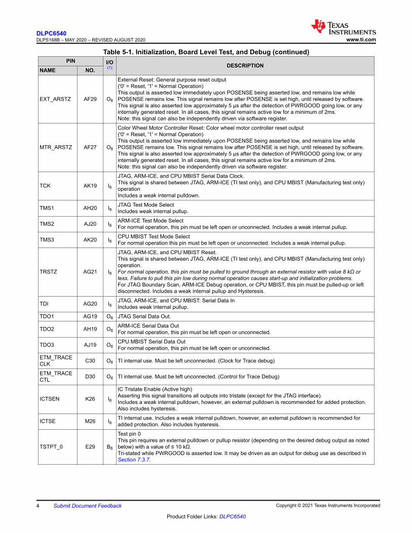
Table 5-1. Initialization, Board Level Test, and Debug (continued)PIN I/O
(1) DESCRIPTIONNAME NO.
EXT_ARSTZ AF29 O8
External Reset: General purpose reset output('0' = Reset, '1' = Normal Operation)This output is asserted low immediately upon POSENSE being asserted low, and remains low whilePOSENSE remains low. This signal remains low after POSENSE is set high, until released by software.This signal is also asserted low approximately 5 µs after the detection of PWRGOOD going low, or anyinternally generated reset. In all cases, this signal remains active low for a minimum of 2ms.Note: this signal can also be independently driven via software register.
MTR_ARSTZ AF27 O8
Color Wheel Motor Controller Reset: Color wheel motor controller reset output('0' = Reset, '1' = Normal Operation)This output is asserted low immediately upon POSENSE being asserted low, and remains low whilePOSENSE remains low. This signal remains low after POSENSE is set high, until released by software.This signal is also asserted low approximately 5 µs after the detection of PWRGOOD going low, or anyinternally generated reset. In all cases, this signal remains active low for a minimum of 2ms.Note: this signal can also be independently driven via software register.
TCK AK19 I8
JTAG, ARM-ICE, and CPU MBIST Serial Data Clock.This signal is shared between JTAG, ARM-ICE (TI test only), and CPU MBIST (Manufacturing test only)operationIncludes a weak internal pulldown.
TMS1 AH20 I8JTAG Test Mode SelectIncludes weak internal pullup.
TMS2 AJ20 I8ARM-ICE Test Mode SelectFor normal operation, this pin must be left open or unconnected. Includes a weak internal pullup.
TMS3 AK20 I8CPU MBIST Test Mode SelectFor normal operation this pin must be left open or unconnected. Includes a weak internal pullup.
TRSTZ AG21 I8
JTAG, ARM-ICE, and CPU MBIST Reset.This signal is shared between JTAG, ARM-ICE (TI test only), and CPU MBIST (Manufacturing test only)operation.For normal operation, this pin must be pulled to ground through an external resistor with value 8 kΩ orless. Failure to pull this pin low during normal operation causes start-up and initialization problems.For JTAG Boundary Scan, ARM-ICE Debug operation, or CPU MBIST, this pin must be pulled-up or leftdisconnected. Includes a weak internal pullup and Hysteresis.
TDI AG20 I8JTAG, ARM-ICE, and CPU MBIST: Serial Data InIncludes weak internal pullup.
TDO1 AG19 O8 JTAG Serial Data Out.
TDO2 AH19 O8ARM-ICE Serial Data OutFor normal operation, this pin must be left open or unconnected.
TDO3 AJ19 O8CPU MBIST Serial Data OutFor normal operation, this pin must be left open or unconnected.
ETM_TRACECLK C30 O8 TI internal use. Must be left unconnected. (Clock for Trace debug)
ETM_TRACECTL D30 O8 TI internal use. Must be left unconnected. (Control for Trace Debug)
ICTSEN K26 I8
IC Tristate Enable (Active high)Asserting this signal transitions all outputs into tristate (except for the JTAG interface).Includes a weak internal pulldown, however, an external pulldown is recommended for added protection.Also includes hysteresis.
ICTSE M26 I8TI internal use. Includes a weak internal pulldown, however, an external pulldown is recommended foradded protection. Also includes hysteresis.
TSTPT_0 E29 B8
Test pin 0This pin requires an external pulldown or pullup resistor (depending on the desired debug output as notedbelow) with a value of ≤ 10 kΩ.Tri-stated while PWRGOOD is asserted low. It may be driven as an output for debug use as described inSection 7.3.7.
DLPC6540DLPS168B – MAY 2020 – REVISED AUGUST 2020 www.ti.com
4 Submit Document Feedback Copyright © 2021 Texas Instruments Incorporated
Product Folder Links: DLPC6540

Table 5-1. Initialization, Board Level Test, and Debug (continued)PIN I/O
(1) DESCRIPTIONNAME NO.
TSTPT_1 E30 B8
Test pin 1This pin requires an external pulldown or pullup resistor (depending on the desired debug output as notedbelow) with a value of ≤ 10 kΩ.Tri-stated while PWRGOOD is asserted low. It may be driven as an output for debug use as described inSection 7.3.7.
TSTPT_2 F26 B8
Test pin 2This pin requires an external pulldown or pullup resistor (depending on the desired debug output as notedbelow) with a value of ≤ 10 kΩ.Tri-stated while PWRGOOD is asserted low. It can be driven as an output for debug use as described inSection 7.3.7.
TSTPT_3 F27 B8
Test pin 3This pin requires an external pulldown or pullup resistor (depending on the desired debug output as notedbelow) with a value of ≤ 10 kΩ.Tri-stated while PWRGOOD is asserted low. It may be driven as an output for debug use as described inSection 7.3.7.
TSTPT_4 F28 B8
Test pin 4This pin requires an external pulldown resistor (≤ 10 kΩ).Tri-stated while PWRGOOD is asserted low. It can be driven as an output for debug use as described inSection 7.3.7.
TSTPT_5 F29 B8
Test pin 5This pin requires an external pulldown resistor (≤ 10 kΩ).Tri-stated while PWRGOOD is asserted low. It can be driven as an output for debug use as described inSection 7.3.7.
TSTPT_6 G26 B8
Test pin 6This pin requires an external pulldown resistor (≤ 10 kΩ).Tri-stated while PWRGOOD is asserted low. It can be driven as an output for debug use as described inSection 7.3.7.
TSTPT_7 G28 B8
Test pin 7This pin requires an external pulldown resistor (≤ 10 kΩ).Tri-stated while PWRGOOD is asserted low. It can be driven as an output for debug use as described inSection 7.3.7.
HWTEST_EN L26 I8Manufacturing test enable signal.This signal must be connected directly to ground on the PCB for normal operation.Includes weak internal pulldown and hysteresis.
(1) See Table 5-13 for more information on I/O definitions.
Table 5-2. Analog Front End (Not Supported in DLPC6540)PIN I/O
(1) DESCRIPTIONNAME NO.AFE_ARSTZ K2 O8 Reserved.
AFE_CLK K3 O8 Reserved.
AFE_IRQ K4 I8 Reserved.
ALF_VSYNC K5 I8 Reserved.
ALF_HSYNC J1 I8 Reserved.
ALF_CSYNC J2 I8 Reserved.
(1) See Table 5-13 for more information on I/O definitions.
www.ti.comDLPC6540
DLPS168B – MAY 2020 – REVISED AUGUST 2020
Copyright © 2021 Texas Instruments Incorporated Submit Document Feedback 5
Product Folder Links: DLPC6540

Table 5-3. V-by-One Interface Input Data and ControlPIN I/O
(1) DESCRIPTION (2) (3)NAME NO.VX1_DATA0_PVX1_DATA0_NVX1_DATA1_PVX1_DATA1_NVX1_DATA2_PVX1_DATA2_NVX1_DATA3_PVX1_DATA3_NVX1_DATA4_PVX1_DATA4_NVX1_DATA5_PVX1_DATA5_NVX1_DATA6_PVX1_DATA6_NVX1_DATA7_PVX1_DATA7_N
C18D18A19B19C20D20A21B21C22D22A23B23C24D24A25B25
I1 V-by-One interface data lanes.
VX1_HTPDN E17 O4
V-by-One interface hot plug detect (controller receiver pulls this signal low to indicate itspresence to the transmitter)This signal is open drain at the controller output. A pullup resistor is required at the transmitter.
VX1_LOCKN E19 O4
V-by-One interface clock detect lock (controller receiver pulls this signal low to indicate clockextraction lock to the transmitter)This signal is open drain at the controller output. A pullup resistor is required at the transmitter.
VX1_CM_CKREF0VX1_CM_CKREF1VX1_CM_CKREF2VX1_CM_CKREF3
E20E21E23E24
I1 V-by-One reserved: Tie these reserved pins to ground.
VX1_CM_AMOUT0VX1_CM_AMOUT1VX1_CM_AMOUT2VX1_CM_AMOUT3
F19F21F22F23
O1 V-by-One reserved: These pins are reserved and must remain unconnected
(1) See Table 5-13 for more information on I/O definitions.(2) The system supports 1 lane, 2 lane, 4 lane, or 8 lane operation, based on the bandwidth requirement of the input source. The inputs
for any un-used data lanes must be left open.(3) The V-by-One port supports limited lane remapping to help optimize board layout. The details are described in Section 7.3.3.
Table 5-4. OpenLDI (FPD-Link I) (Not Supported in DLPC6540) Ports Input Data and ControlPIN I/O
(1) DESCRIPTION(2) (3)NAME NO.FPDA_CLK_PFPDA_CLK_N
H3H4 I5 Reserved.
FPDA_DATAA_PFPDA_DATAA_NFPDA_DATAB_PFPDA_DATAB_NFPDA_DATAC_PFPDA_DATAC_NFPDA_DATAD_PFPDA_DATAD_NFPDA_DATAE_PFPDA_DATAE_N
G1G2F3F4E1E2D3D4C1C2
I5 Reserved.
FPDB_CLK_PFPDB_CLK_N
A4B4 I5 Reserved.
DLPC6540DLPS168B – MAY 2020 – REVISED AUGUST 2020 www.ti.com
6 Submit Document Feedback Copyright © 2021 Texas Instruments Incorporated
Product Folder Links: DLPC6540

Table 5-4. OpenLDI (FPD-Link I) (Not Supported in DLPC6540) Ports Input Data and Control (continued)PIN I/O
(1) DESCRIPTION(2) (3)NAME NO.FPDB_DATAA_PFPDB_DATAA_NFPDB_DATAB_PFPDB_DATAB_NFPDB_DATAC_PFPDB_DATAC_NFPDB_DATAD_PFPDB_DATAD_NFPDB_DATAE_PFPDB_DATAE_N
C5D5A6B6C7D7A8B8C9D9
I5 Reserved.
FPDC_CLK_PFPDC_CLK_N
A10B10 I5 Reserved.
FPDC_DATAA_PFPDC_DATAA_NFPDC_DATAB_PFPDC_DATAB_NFPDC_DATAC_PFPDC_DATAC_NFPDC_DATAD_PFPDC_DATAD_NFPDC_DATAE_PFPDC_DATAE_N
C11D11A12B12C13D13A14B14C15D15
I5 Reserved.
(1) See Table 5-13 for more information on I/O definitions.(2) Throughout this document the terms FPD and FPD-Link refer to OpenLDI (FPD-Link I).(3) Tie the inputs for any un-used port(s) to ground, or pull to ground through an external resistor.
Table 5-5. Parallel Port Input Data and Control (Not Supported in DLPC6540)PIN I/O
(1)DESCRIPTION
PARALLEL RGB MODE NAME NO.PCLK (FPDB_DATAB_N) B6 I6 Reserved.
VSYNC (FPDA_DATAE_P) C1 I6 Reserved.
HSYNC (FPDA_DATAE_N) C2 I6 Reserved.
DATEN (FPDB_DATAE_N) D9 I6 Reserved. (2)
FIELD (FPDC_DATAE_P) C15 I6 Reserved.
3D_REF (FPDC_DATAE_N) D15 I6 Reserved.
PDATA_A0 (FPDA_CLK_P)PDATA_A1 (FPDA_CLK_N)PDATA_A2 (FPDA_DATAA_P)PDATA_A3 (FPDA_DATAA_N)PDATA_A4 (FPDA_DATAB_P)PDATA_A5 (FPDA_DATAB_N)PDATA_A6 (FPDA_DATAC_P)PDATA_A7 (FPDA_DATAC_N)PDATA_A8 (FPDA_DATAD_P)PDATA_A9 (FPDA_DATAD_N)
H3H4G1G2F3F4E1E2D3D4
I6 Reserved.
PDATA_B0 (FPDB_CLK_P)PDATA_B1 (FPDB_CLK_N)PDATA_B2 (FPDB_DATAA_P)PDATA_B3 (FPDB_DATAA_N)PDATA_B4 (FPDB_DATAB_P)PDATA_B5 (FPDB_DATAC_P)PDATA_B6 (FPDB_DATAC_N)PDATA_B7 (FPDB_DATAD_P)PDATA_B8 (FPDB_DATAD_N)PDATA_B9 (FPDB_DATAE_P)
A4B4C5D5A6C7D7A8B8C9
I6 Reserved.
www.ti.comDLPC6540
DLPS168B – MAY 2020 – REVISED AUGUST 2020
Copyright © 2021 Texas Instruments Incorporated Submit Document Feedback 7
Product Folder Links: DLPC6540

Table 5-5. Parallel Port Input Data and Control (Not Supported in DLPC6540) (continued)PIN I/O
(1)DESCRIPTION
PARALLEL RGB MODE NAME NO.PDATA_C0 (FPDC_CLK_P)PDATA_C1 (FPDC_CLK_N)PDATA_C2 (FPDC_DATAA_P)PDATA_C3 (FPDC_DATAA_N)PDATA_C4 (FPDC_DATAB_P)PDATA_C5 (FPDC_DATAB_N)PDATA_C6 (FPDC_DATAC_P)PDATA_C7 (FPDC_DATAC_N)PDATA_C8 (FPDC_DATAD_P)PDATA_C9 (FPDC_DATAD_N)
A10B10C11D11A12B12C13D13A14B14
I6 Reserved.
(1) See Table 5-13 for more information on I/O definitions.(2) If the DATEN is not actively driven, then it must be pulled up to 3.3V with a weak pull up resistor (50k Ohm max).
Table 5-6. DMD Reset and Low Speed InterfacesPIN I/O
(1) DESCRIPTIONNAME NO.DMD_LS0_CLK_PDMD_LS0_CLK_N
AH17AG17 O2 DMD low speed differential interface, Port 0 Clock
DMD_LS0_WDATA_PDMD_LS0_WDATA_N
AK16AJ16 O2 DMD low speed differential interface, Port 0 Write Data
DMD_LS1_CLK_PDMD_LS1_CLK_N
AH15AG15 O2 DMD low speed differential interface, Port 1 Clock (2)
DMD_LS1_WDATA_PDMD_LS1_WDATA_N
AK14AJ14 O2 DMD low speed differential interface, Port 1Write Data (2)
DMD_LS0_RDATA AH13 I3 DMD, low speed single ended serial interface, Port 0 Read Data (3)
DMD_LS1_RDATA AG13 I3DMD, low speed single ended serial interface, Port 1 Read Data (2) (3). If this portnot used, this signal requires an external pullup or pulldown to keep this inputfrom floating.
DMD_DEN_ARSTZ AK12 O3
DMD driver enable signal / Active Low Asynchronous Reset('1' = Enabled, '0' = Reset)This signal is driven low after the DMD is parked and before power is removedfrom the DMD.If the 1.8-V power to the DLPC6540 is independent of the 1.8-V power to theDMD, then an external pulldown resistor must be used to hold the signal low inthe event the DLPC6540 power is inactive while DMD power is applied.
(1) See Table 5-13 for more information on I/O definitions.(2) DMD LS1 port is reserved for single controller, two DMD applications.(3) All control interface reads make use of the single ended low speed signals. The read data is clocked by the low speed differential
write clock.
Table 5-7. DMD HSSI (High Speed Serial Interface)PIN (1) I/O
(2) DESCRIPTIONNAME NO.DMD_HSSI0_CLK_PDMD_HSSI0_CLK_N
AK25AJ25 O7 DMD high speed serial interface, Port 0 Clock Lane.
DLPC6540DLPS168B – MAY 2020 – REVISED AUGUST 2020 www.ti.com
8 Submit Document Feedback Copyright © 2021 Texas Instruments Incorporated
Product Folder Links: DLPC6540
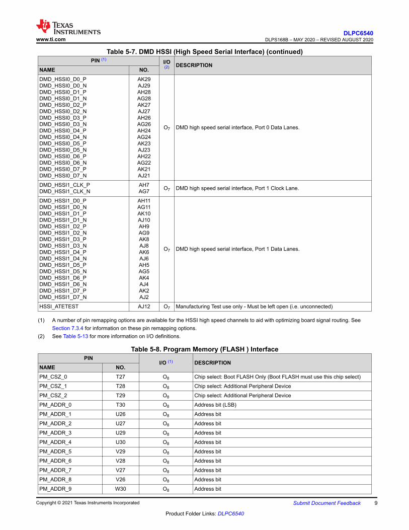
Table 5-7. DMD HSSI (High Speed Serial Interface) (continued)PIN (1) I/O
(2) DESCRIPTIONNAME NO.DMD_HSSI0_D0_PDMD_HSSI0_D0_NDMD_HSSI0_D1_PDMD_HSSI0_D1_NDMD_HSSI0_D2_PDMD_HSSI0_D2_NDMD_HSSI0_D3_PDMD_HSSI0_D3_NDMD_HSSI0_D4_PDMD_HSSI0_D4_NDMD_HSSI0_D5_PDMD_HSSI0_D5_NDMD_HSSI0_D6_PDMD_HSSI0_D6_NDMD_HSSI0_D7_PDMD_HSSI0_D7_N
AK29AJ29AH28AG28AK27AJ27AH26AG26AH24AG24AK23AJ23AH22AG22AK21AJ21
O7 DMD high speed serial interface, Port 0 Data Lanes.
DMD_HSSI1_CLK_PDMD_HSSI1_CLK_N
AH7AG7 O7 DMD high speed serial interface, Port 1 Clock Lane.
DMD_HSSI1_D0_PDMD_HSSI1_D0_NDMD_HSSI1_D1_PDMD_HSSI1_D1_NDMD_HSSI1_D2_PDMD_HSSI1_D2_NDMD_HSSI1_D3_PDMD_HSSI1_D3_NDMD_HSSI1_D4_PDMD_HSSI1_D4_NDMD_HSSI1_D5_PDMD_HSSI1_D5_NDMD_HSSI1_D6_PDMD_HSSI1_D6_NDMD_HSSI1_D7_PDMD_HSSI1_D7_N
AH11AG11AK10AJ10AH9AG9AK8AJ8AK6AJ6AH5AG5AK4AJ4AK2AJ2
O7 DMD high speed serial interface, Port 1 Data Lanes.
HSSI_ATETEST AJ12 O7 Manufacturing Test use only - Must be left open (i.e. unconnected)
(1) A number of pin remapping options are available for the HSSI high speed channels to aid with optimizing board signal routing. SeeSection 7.3.4 for information on these pin remapping options.
(2) See Table 5-13 for more information on I/O definitions.
Table 5-8. Program Memory (FLASH ) InterfacePIN
I/O (1) DESCRIPTIONNAME NO.PM_CSZ_0 T27 O8 Chip select: Boot FLASH Only (Boot FLASH must use this chip select)
PM_CSZ_1 T28 O8 Chip select: Additional Peripheral Device
PM_CSZ_2 T29 O8 Chip select: Additional Peripheral Device
PM_ADDR_0 T30 O8 Address bit (LSB)
PM_ADDR_1 U26 O8 Address bit
PM_ADDR_2 U27 O8 Address bit
PM_ADDR_3 U29 O8 Address bit
PM_ADDR_4 U30 O8 Address bit
PM_ADDR_5 V29 O8 Address bit
PM_ADDR_6 V28 O8 Address bit
PM_ADDR_7 V27 O8 Address bit
PM_ADDR_8 V26 O8 Address bit
PM_ADDR_9 W30 O8 Address bit
www.ti.comDLPC6540
DLPS168B – MAY 2020 – REVISED AUGUST 2020
Copyright © 2021 Texas Instruments Incorporated Submit Document Feedback 9
Product Folder Links: DLPC6540
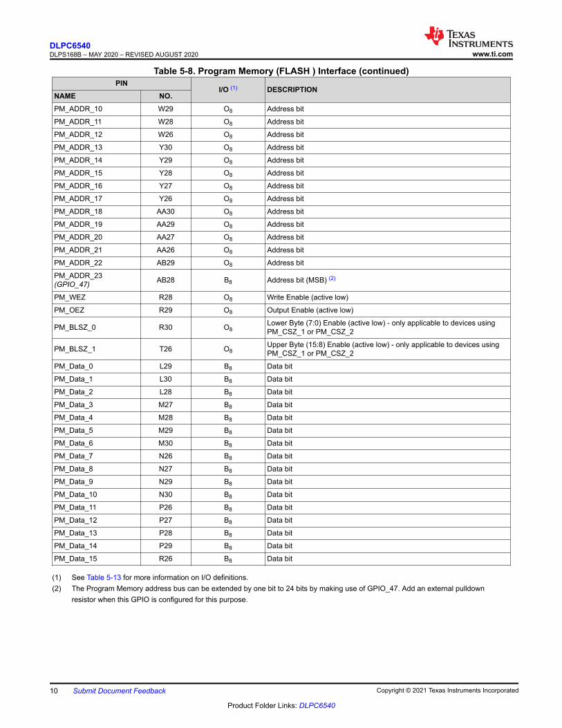
Table 5-8. Program Memory (FLASH ) Interface (continued)PIN
I/O (1) DESCRIPTIONNAME NO.PM_ADDR_10 W29 O8 Address bit
PM_ADDR_11 W28 O8 Address bit
PM_ADDR_12 W26 O8 Address bit
PM_ADDR_13 Y30 O8 Address bit
PM_ADDR_14 Y29 O8 Address bit
PM_ADDR_15 Y28 O8 Address bit
PM_ADDR_16 Y27 O8 Address bit
PM_ADDR_17 Y26 O8 Address bit
PM_ADDR_18 AA30 O8 Address bit
PM_ADDR_19 AA29 O8 Address bit
PM_ADDR_20 AA27 O8 Address bit
PM_ADDR_21 AA26 O8 Address bit
PM_ADDR_22 AB29 O8 Address bit
PM_ADDR_23(GPIO_47) AB28 B8 Address bit (MSB) (2)
PM_WEZ R28 O8 Write Enable (active low)
PM_OEZ R29 O8 Output Enable (active low)
PM_BLSZ_0 R30 O8Lower Byte (7:0) Enable (active low) - only applicable to devices usingPM_CSZ_1 or PM_CSZ_2
PM_BLSZ_1 T26 O8Upper Byte (15:8) Enable (active low) - only applicable to devices usingPM_CSZ_1 or PM_CSZ_2
PM_Data_0 L29 B8 Data bit
PM_Data_1 L30 B8 Data bit
PM_Data_2 L28 B8 Data bit
PM_Data_3 M27 B8 Data bit
PM_Data_4 M28 B8 Data bit
PM_Data_5 M29 B8 Data bit
PM_Data_6 M30 B8 Data bit
PM_Data_7 N26 B8 Data bit
PM_Data_8 N27 B8 Data bit
PM_Data_9 N29 B8 Data bit
PM_Data_10 N30 B8 Data bit
PM_Data_11 P26 B8 Data bit
PM_Data_12 P27 B8 Data bit
PM_Data_13 P28 B8 Data bit
PM_Data_14 P29 B8 Data bit
PM_Data_15 R26 B8 Data bit
(1) See Table 5-13 for more information on I/O definitions.(2) The Program Memory address bus can be extended by one bit to 24 bits by making use of GPIO_47. Add an external pulldown
resistor when this GPIO is configured for this purpose.
DLPC6540DLPS168B – MAY 2020 – REVISED AUGUST 2020 www.ti.com
10 Submit Document Feedback Copyright © 2021 Texas Instruments Incorporated
Product Folder Links: DLPC6540

Table 5-9. Peripheral InterfacesPIN
I/O (1) DESCRIPTIONNAME NO.
IIC0_SCL E27 B13
I2C Port 0 (Master-Slave), Typically slave for Host Command and Control to Controller, SCL(bidirectional, open-drain): An external pullup is required. The minimum acceptable value for thispullup is 1KΩ .
IIC0_SDA D29 B13
I2C Port 0 (Master-Slave), Typically slave for Host Command and Control to Controller, SDA.(bidirectional, open-drain): An external pullup is required. The minimum acceptable value for thispullup is 1KΩ
SSP0_TXD AD27 O8 SSP/SPI Port 0 Data Out (Master): Transmit data pin
SSP0_RXD AD29 I8 SSP/SPI Port 0 Data In (Master): Receive data pin
SSP0_CLK AD28 O8 SSP/SPI Port 0 Clock (Master): Clock pin
SSP0_CSZ_2 AC28 O8
SPI Port 0 chip select 2 (Master): Chip select (Active Low)An external pullup resistor (≤ 10 kΩ) is suggested to avoid a floating chip select input to theexternal device
SSP0_CSZ_1 AC26 O8
SPI Port 0 chip select 1 (Master): Chip select (Active Low)An external pullup resistor (≤ 10 kΩ) is suggested to avoid a floating chip select input to theexternal device
SSP0_CSZ_0 AB27 O8
SPI Port 0 chip select 0 (Master): Chip select (Active Low)An external pullup resistor (≤ 10 kΩ) is suggested to avoid a floating chip select input to theexternal device
UART0_TXD P4 O8UART Port 0 (Slave): Serial Data TransmitThis UART port is reserved for TI debug. An external pullup resistor (≤ 10 kΩ) is required
UART0_RXD P5 I8UART Port 0 (Slave): Serial Data ReceiveThis UART port is reserved for TI debug. An external pullup resistor (≤ 10 kΩ) is required
UART0_RTSZ N2 O8UART Port 0 (Slave): Ready To Send (Hardware flow control signal (Active Low))This UART port is reserved for TI debug. An external pullup resistor (≤ 10 kΩ) is required
UART0_CTSZ N3 I8UART Port 0 (Slave): Clear to Send (Hardware flow control signal (Active Low))This UART port is reserved for TI debug. An external pullup resistor (≤ 10 kΩ) is required
USB_DAT_PUSB_DAT_N
B27A27 B11 USB OTG Data Lane (Master-Stave)
USB_VBUS D26 B11 USB OTG 5V Power Supply Detection (Master-Slave)
USB_ID C27 IOther USB OTG Mini Receptacle Identification (Master-Slave)
USB_TXRTUNE C26 BGNDUSB OTG Reference ResistorAn external reference resistor must be connected as shown in Section 10.1.6
USB_XI A29 IGNDUSB OTG External Oscillator XI - Not used (clock provided internally)For normal operation this pin must be connected to GND.
USB_XO B29 BGNDUSB OTG External Oscillator XO - Not used (clock provided internally)For normal operation this pin must be left open (unconnected).
USB_ANALOGTEST C28 BOtherUSB OTG Manufacturing TestThis pin must be left open (unconnected)
PMD_INTZ AD26 I8 Reserved Function. This signal requires an external pullup.
CW_PWM AE30 O8 Reserved Function.
CW_INDEX AE29 I8 Reserved Function.
(1) See Table 5-13 for more information on I/O definitions.
Table 5-10. GPIO Peripheral InterfacePIN I/O
(1) DESCRIPTION(2) (3) (4)NAME NO.
GPIO_87 K1 B8
General purpose I/O 87: Options:1. Alt 0: Reserved2. Alt 1: DAO_CLKIN (I)3. Optional GPIO
www.ti.comDLPC6540
DLPS168B – MAY 2020 – REVISED AUGUST 2020
Copyright © 2021 Texas Instruments Incorporated Submit Document Feedback 11
Product Folder Links: DLPC6540

Table 5-10. GPIO Peripheral Interface (continued)PIN I/O
(1) DESCRIPTION(2) (3) (4)NAME NO.
GPIO_86 L5 B8
General purpose I/O 86: Options:1. Alt 0: Reserved2. Alt 1: DAO_DI_1 (I)3. Optional GPIO
GPIO_85 L4 B8
General purpose I/O 85: Options:1. Alt 0: Reserved2. Alt 1: DAO_DI_0 (I)3. Optional GPIO
GPIO_84 L3 B8
General purpose I/O 84: Options:1. Alt 0: Reserved2. Alt 1: HBT_CLKIN_2 (I)3. Optional GPIO
GPIO_83 L2 B8
General purpose I/O 83: Options:1. Alt 0: Reserved2. Alt 1: HBT_DI_2 (I)3. Optional GPIO
GPIO_82 M5 B8
General purpose I/O 82: Options:1. Alt 0: Reserved2. Alt 1: HBT_CLKIN_1 (I)3. Optional GPIO
GPIO_81 M4 B8
General purpose I/O 81: Options:1. Alt 0: Reserved2. Alt 1: HBT_DI_1 (I)3. Optional GPIO
GPIO_80 M2 B8
General purpose I/O 80: Options:1. Alt 0: Reserved2. Alt 1: HBT_CLKIN_0 (I)3. Optional GPIO
GPIO_79 M1 B8
General purpose I/O 79: Options:1. Alt 0: Reserved2. Alt 1: HBT_DI_0 (I)3. Optional GPIO
GPIO_78 N5 B8
General purpose I/O 78: Options:1. Alt 0: Reserved2. Alt 1: SEQ_SYNC (B/ OpenDrain)3. Optional GPIO
GPIO_77 N4 B8
General purpose I/O 77: Options:1. Alt 0: Reserved2. Alt 1: EFSYNC (O)/ DASYNC (I)3. Optional GPIO
GPIO_76 AD5 B8
General purpose I/O 76: Options:1. Alt 0: AWC1_DACD_PWMB_1 (O)2. Alt 1: N/A3. Optional GPIO
DLPC6540DLPS168B – MAY 2020 – REVISED AUGUST 2020 www.ti.com
12 Submit Document Feedback Copyright © 2021 Texas Instruments Incorporated
Product Folder Links: DLPC6540

Table 5-10. GPIO Peripheral Interface (continued)PIN I/O
(1) DESCRIPTION(2) (3) (4)NAME NO.
GPIO_75 AC1 B8
General purpose I/O 75: Options:1. Alt 0: AWC1_DACS_PWMA_1 (O)2. Alt 1: N/A3. Optional GPIO
GPIO_74 AC2 B8
General purpose I/O 74: Options:1. Alt 0: AWC1_DACD_PWMB_0 (O)2. Alt 1: N/A3. Optional GPIO
GPIO_73 AC4 B8
General purpose I/O 73: Options:1. Alt 0: AWC1_DACS_PWMA_0 (O)2. Alt 1: N/A3. Optional GPIO
GPIO_72 AC5 B8
General purpose I/O 72: Options:1. Alt 0: AWC1_DACCLK_0_1 (O)2. Alt 1: N/A3. Optional GPIO
GPIO_71 AD1 B8
General purpose I/O 71: Options:1. Alt 0: AWC1_OUT_ENZ (O)2. Alt 1: N/A3. Optional GPIO
GPIO_70 AD2 B8
General purpose I/O 70: Options:1. Alt 0: AWC0_DACD_PWMB_1 (O)2. Alt 1: N/A3. Optional GPIO
GPIO_69 AD3 B8
General purpose I/O 69: Options:1. Alt 0: AWC0_DACS_PWMA_1 (O)2. Alt 1: MEMAUX_1 (O) (#2)3. Optional GPIO
GPIO_68 AD4 B8
General purpose I/O 68: Options:1. Alt 0: AWC0_DACD_PWMB_0 (O)2. Alt 1: IIC2_SDA (B) (#3)3. Optional GPIO
GPIO_67 AF4 B8
General purpose I/O 67: Options:1. Alt 0: AWC0_DACS_PWMA_0 (O)2. Alt 1: IIC2_SCL (B) (#3)3. Optional GPIO
GPIO_66 AE2 B8
General purpose I/O 66: Options:1. Alt 0: AWC0_DACCLK_0_1 (O)2. Alt 1: N/A3. Optional GPIO
GPIO_65 AE3 B8
General purpose I/O 65: Options:1. Alt 0: AWC0_OUT_ENZ (O)2. Alt 1: N/A3. Optional GPIO
www.ti.comDLPC6540
DLPS168B – MAY 2020 – REVISED AUGUST 2020
Copyright © 2021 Texas Instruments Incorporated Submit Document Feedback 13
Product Folder Links: DLPC6540
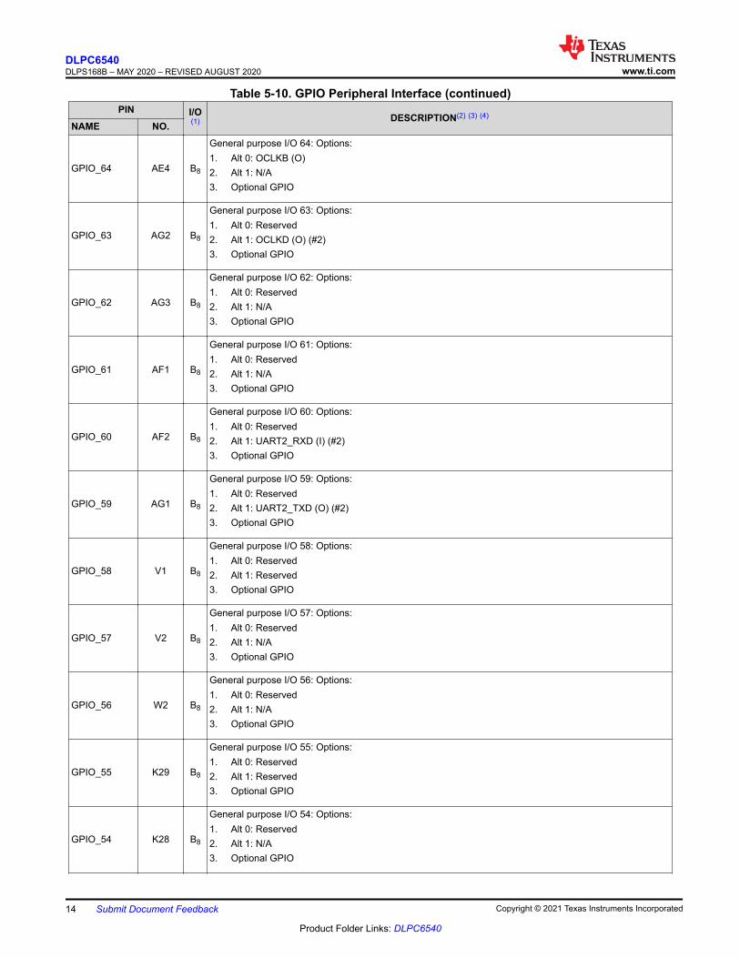
Table 5-10. GPIO Peripheral Interface (continued)PIN I/O
(1) DESCRIPTION(2) (3) (4)NAME NO.
GPIO_64 AE4 B8
General purpose I/O 64: Options:1. Alt 0: OCLKB (O)2. Alt 1: N/A3. Optional GPIO
GPIO_63 AG2 B8
General purpose I/O 63: Options:1. Alt 0: Reserved2. Alt 1: OCLKD (O) (#2)3. Optional GPIO
GPIO_62 AG3 B8
General purpose I/O 62: Options:1. Alt 0: Reserved2. Alt 1: N/A3. Optional GPIO
GPIO_61 AF1 B8
General purpose I/O 61: Options:1. Alt 0: Reserved2. Alt 1: N/A3. Optional GPIO
GPIO_60 AF2 B8
General purpose I/O 60: Options:1. Alt 0: Reserved2. Alt 1: UART2_RXD (I) (#2)3. Optional GPIO
GPIO_59 AG1 B8
General purpose I/O 59: Options:1. Alt 0: Reserved2. Alt 1: UART2_TXD (O) (#2)3. Optional GPIO
GPIO_58 V1 B8
General purpose I/O 58: Options:1. Alt 0: Reserved2. Alt 1: Reserved3. Optional GPIO
GPIO_57 V2 B8
General purpose I/O 57: Options:1. Alt 0: Reserved2. Alt 1: N/A3. Optional GPIO
GPIO_56 W2 B8
General purpose I/O 56: Options:1. Alt 0: Reserved2. Alt 1: N/A3. Optional GPIO
GPIO_55 K29 B8
General purpose I/O 55: Options:1. Alt 0: Reserved2. Alt 1: Reserved3. Optional GPIO
GPIO_54 K28 B8
General purpose I/O 54: Options:1. Alt 0: Reserved2. Alt 1: N/A3. Optional GPIO
DLPC6540DLPS168B – MAY 2020 – REVISED AUGUST 2020 www.ti.com
14 Submit Document Feedback Copyright © 2021 Texas Instruments Incorporated
Product Folder Links: DLPC6540

Table 5-10. GPIO Peripheral Interface (continued)PIN I/O
(1) DESCRIPTION(2) (3) (4)NAME NO.
GPIO_53 W3 B8
General purpose I/O 53: Options:1. Alt 0: Reserved2. Alt 1: LED_DRIVER_ON (O)3. Optional GPIO
GPIO_52 W4 B8
General purpose I/O 52: Options:1. Alt 0: Reserved2. Alt 1: N/A3. Optional GPIO
GPIO_51 V5 B8
General purpose I/O 51: Options:1. Alt 0: Reserved2. Alt 1: DMD_PWR_EN (O)3. Optional GPIO
GPIO_50 AC29 B8
General purpose I/O 50: Options:1. Alt 0: SSP0_CSZ_3 (O)2. Alt 1: N/A3. Optional GPIO
GPIO_49 AC30 B8
General purpose I/O 49: Options:1. Alt 0: SSP0_CSZ_4 (O)2. Alt 1: N/A3. Optional GPIO
GPIO_48 AB26 B8
General purpose I/O 48: Options:1. Alt 0: USB OTG External USB Switch Control (O)2. Alt 1: N/A3. Optional GPIO
GPIO_47 AB28 B8
General purpose I/O 47: Options:1. Alt 0: PM_ADDR_23 (O)2. Alt 1: N/A3. Optional GPIO
GPIO_46 K27 B8
General purpose I/O 46: Options:1. Alt 0: Reserved2. Alt 1: SSP2_BC_CSZ (O-MST/I-SLV)3. Optional GPIO
GPIO_45 J30 B8
General purpose I/O 45: Options:1. Alt 0: Reserved2. Alt 1: SSP2_CSZ_2 (O-MST/I-SLV)3. Optional GPIO
GPIO_44 J29 B8
General purpose I/O 44: Options:1. Alt 0: OCLKC (O) (#1)2. Alt 1: SSP2_CSZ_1 (O-MST/I-SLV)3. Optional GPIO
GPIO_43 J27 B8
General purpose I/O 43: Options:1. Alt 0: OCLKD (O) (#1)2. Alt 1: SSP2_CSZ_0 (O-MST/I-SLV)3. Optional GPIO
www.ti.comDLPC6540
DLPS168B – MAY 2020 – REVISED AUGUST 2020
Copyright © 2021 Texas Instruments Incorporated Submit Document Feedback 15
Product Folder Links: DLPC6540

Table 5-10. GPIO Peripheral Interface (continued)PIN I/O
(1) DESCRIPTION(2) (3) (4)NAME NO.
GPIO_42 J26 B8
General purpose I/O 42: Options:1. Alt 0: IIC2_SDA (B) (#1)2. Alt 1: SSP2_DO (O)3. Optional GPIO
GPIO_41 H30 B8
General purpose I/O 41: Options:1. Alt 0: IIC2_SCL (B) (#1)2. Alt 1: SSP2_DI (I)3. Optional GPIO
GPIO_40 H29 B8
General purpose I/O 40: Options:1. Alt 0: MEMAUX_1 (O) (#1)2. Alt 1: SSP2_SCLK (O-MST/I-SLV)3. Optional GPIO
GPIO_39 H28 B8
General purpose I/O 39: Options:1. Alt 0: UART2_RXD (I) (#1)2. Alt 1: HBT_CLKOUT (O)3. Optional GPIO
GPIO_38 H27 B8
General purpose I/O 38: Options:1. Alt 0: UART2_TXD (O) (#1)2. Alt 1: HBT_DO (O)3. Optional GPIO
GPIO_37 H26 B8
General purpose I/O 37: Options:1. Alt 0: Reserved2. Alt 1: DAO_CLKOUT (O)3. Optional GPIO
GPIO_36 G30 B8
General purpose I/O 36: Options:1. Alt 0: Reserved2. Alt 1: DAO_DO_1 (O)3. Optional GPIO
GPIO_35 G29 B8
General purpose I/O 35: Options:1. Alt 0: OCLKC (O) (#2)2. Alt 1: DAO_DO_0 (O)3. Optional GPIO
GPIO_34 Y1 B8
General purpose I/O 34: Options:1. Alt 0: WRP_CAMERA_TRIG (O)2. Alt 1: N/A3. Optional GPIO
GPIO_33 Y2 B8
General purpose I/O 33: Options:1. Alt 0: PAUX11 (O)2. Alt 1: IIC2_SDA (B) (#2)3. Optional GPIO
GPIO_32 Y4 B8
General purpose I/O 32: Options:1. Alt 0: PAUX10 (O)2. Alt 1: IIC2_SCL (B) (#2)3. Optional GPIO
DLPC6540DLPS168B – MAY 2020 – REVISED AUGUST 2020 www.ti.com
16 Submit Document Feedback Copyright © 2021 Texas Instruments Incorporated
Product Folder Links: DLPC6540

Table 5-10. GPIO Peripheral Interface (continued)PIN I/O
(1) DESCRIPTION(2) (3) (4)NAME NO.
GPIO_31 Y5 B8
General purpose I/O 31: Options:1. Alt 0: PAUX9 (O)2. Alt 1: PAUX_INT3 (O)3. Optional GPIO
GPIO_30 AA1 B8
General purpose I/O 30: Options:1. Alt 0: PAUX8 (O)2. Alt 1: PAUX_INT2 (O)3. Optional GPIO
GPIO_29 AA2 B8
General purpose I/O 29: Options:1. Alt 0: PAUX7 (O)2. Alt 1: N/A3. Optional GPIO
GPIO_28 AA3 B8
General purpose I/O 28: Options:1. Alt 0: PAUX6 (O)2. Alt 1: LEDSEL_4 (O)3. Optional GPIO
GPIO_27 AA4 B8
General purpose I/O 27: Options:1. Alt 0: PAUX5 (O)2. Alt 1: LEDSEL_3 (O)3. Optional GPIO
GPIO_26 AA5 B8
General purpose I/O 26: Options:1. Alt 0: PAUX4 (O)2. Alt 1: LEDSEL_2 (O)3. Optional GPIO
GPIO_25 AB2 B8
General purpose I/O 25: Options:1. Alt 0: PAUX3 (O)2. Alt 1: LEDSEL_1 (O)3. Optional GPIO
GPIO_24 AB3 B8
General purpose I/O 24: Options:1. Alt 0: PAUX2 (O)2. Alt 1: LEDSEL_0 (O)3. Optional GPIO
GPIO_23 AB4 B8
General purpose I/O 23: Options:1. Alt 0: PAUX1 (O) SEQ Index2. Alt 1: PAUX_INT1 (O)3. Optional GPIO
GPIO_22 AB5 B8
General purpose I/O 22: Options:1. Alt 0: PAUX0 (O)2. Alt 1: PAUX_INT0 (O)3. Optional GPIO
GPIO_21 P3 B8
General purpose I/O 21: Options:1. Alt 0: PWM-IN1 (I)2. Alt 1: N/A3. Optional GPIO
www.ti.comDLPC6540
DLPS168B – MAY 2020 – REVISED AUGUST 2020
Copyright © 2021 Texas Instruments Incorporated Submit Document Feedback 17
Product Folder Links: DLPC6540

Table 5-10. GPIO Peripheral Interface (continued)PIN I/O
(1) DESCRIPTION(2) (3) (4)NAME NO.
GPIO_20 P2 B8
General purpose I/O 20: Options:1. Alt 0: PWM-IN0 (I)2. Alt 1: N/A3. Optional GPIO
GPIO_19 P1 B8
General purpose I/O 19: Options:1. Alt 0: IR1 (I)2. Alt 1: N/A3. Optional GPIO
GPIO_18 R5 B8
General purpose I/O 18: Options:1. Alt 0: IR0 (I)2. Alt 1: N/A3. Optional GPIO
GPIO_17 R4 B8
General purpose I/O 17: Options:1. Alt 0: N/A2. Alt 1: N/A3. Optional GPIO
GPIO_16 R2 B8
General purpose I/O 16: Options:1. Alt 0: UART1_RTSZ (O)2. Alt 1: N/A3. Optional GPIO
GPIO_15 R1 B8
General purpose I/O 15: Options:1. Alt 0: UART1_CTSZ (I)2. Alt 1: N/A3. Optional GPIO
GPIO_14 T3 B8
General purpose I/O 14: Options:1. Alt 0: UART1_RXD (I)2. Alt 1: N/A3. Optional GPIO
GPIO_13 T4 B8
General purpose I/O 13: Options:1. Alt 0: UART1_TXD (O)2. Alt 1: N/A3. Optional GPIO
GPIO_12 T5 B8
General purpose I/O 12: Options:1. Alt 0: IIC1_SDA (B)2. Alt 1: N/A3. Optional GPIO
GPIO_11 T2 B8
General purpose I/O 11: Options:1. Alt 0: IIC1_SCL (B)2. Alt 1: N/A3. Optional GPIO
GPIO_10 V3 B8
General purpose I/O 10: Options:1. Alt 0: SAS_INTGTR_EN (O)2. Alt 1: N/A3. Optional GPIO
DLPC6540DLPS168B – MAY 2020 – REVISED AUGUST 2020 www.ti.com
18 Submit Document Feedback Copyright © 2021 Texas Instruments Incorporated
Product Folder Links: DLPC6540

Table 5-10. GPIO Peripheral Interface (continued)PIN I/O
(1) DESCRIPTION(2) (3) (4)NAME NO.
GPIO_09 U1 B8
General purpose I/O 09: Options:1. Alt 0: SAS_CSZ (O)2. Alt 1: N/A3. Optional GPIO
GPIO_08 U2 B8
General purpose I/O 08: Options:1. Alt 0: SAS_DO (O)2. Alt 1: N/A3. Optional GPIO
GPIO_07 U4 B8
General purpose I/O 07: Options:1. Alt 0: SAS_DI (I)2. Alt 1: N/A3. Optional GPIO
GPIO_06 V4 B8
General purpose I/O 06: Options:1. Alt 0: SAS_CLK (O)2. Alt 1: N/A3. Optional GPIO
GPIO_05 A17 B8
General purpose I/O 05: Options:1. Alt 0: SSP1_CSZ_2 (O-MST/I-SLV)2. Alt 1: N/A3. Optional GPIO
GPIO_04 B17 B8
General purpose I/O 04: Options:1. Alt 0: SSP1_CSZ_1 (O-MST/I-SLV)2. Alt 1: N/A3. Optional GPIO
GPIO_03 B15 B8
General purpose I/O 03: Options:1. Alt 0: SSP1_CSZ_0 (O-MST/I-SLV)2. Alt 1: N/A3. Optional GPIO
GPIO_02 C16 B8
General purpose I/O 02: Options:1. Alt 0: SSP1_DO (O)2. Alt 1: N/A3. Optional GPIO
GPIO_01 D16 B8
General purpose I/O 01: Options:1. Alt 0: SSP1_DI (I)2. Alt 1: N/A3. Optional GPIO
GPIO_00 E16 B8
General purpose I/O 00: Options:1. Alt 0: SSP1_SCLK (O-MST/I-SLV)2. Alt 1: N/A3. Optional GPIO
(1) See Table 5-13 for more information on I/O definitions.(2) This table defines the GPIO capabilities of the DLPC6540. Please see Section 7.3.6 for specific product configuration allocations of
these GPIO.(3) Most GPIO have at least one alternate hardware functional use in addition to being available as a general purpose I/O. Depending on
the product configuration, GPIO may be reserved specifically for use as an alternate hardware function (and would therefore not be
www.ti.comDLPC6540
DLPS168B – MAY 2020 – REVISED AUGUST 2020
Copyright © 2021 Texas Instruments Incorporated Submit Document Feedback 19
Product Folder Links: DLPC6540

available as a general purpose I/O). More information on GPIO allocations for specific product configurations can be found in Section7.3.6.
(4) All GPIO that are available as a general purpose I/O must be configured as an input, a standard output, or an open-drain output. Thisis set in the flash configuration. Configure unused GPIO as a logic zero output and leave unconnected, otherwise an external pullup orpulldown resistor is required to avoid a floating input. The reset default for all GPIO is as an input signal. An external pullup resistor (≤10 kΩ) is required for each signal configured as open-drain output.
Table 5-11. Clock and SupportPIN I/O
(1) DESCRIPTIONNAME NO.REFCLKA_I AJ18 I9 Crystal A Input: Reference clock crystal input. (2) (3)
REFCLKA_O AK18 O10 Crystal A Output: Reference clock crystal output. (2)
REFCLKB_I B16 I14 Crystal B Input: Reference clock crystal input. (2) (3)
REFCLKB_O A16 O15 Crystal B Output: Reference clock crystal output. (2)
OCLKA AD30 O8
General Purpose Output Clock A (4)
Targeted for driving Color Wheel motor controller. Frequency is software programmable, with apower-up default frequency of 0.77 MHz.Note: the output frequency is not affected by non-power-up reset operations (i.e., the system holdsthe last programmed value until system is power cycled).
(1) See Table 5-13 for more information on I/O definitions.(2) For more information on this signal see Section 6.11(3) For applications where an external oscillator is used in place of a crystal, use an oscillator to drive this pin(4) For more information on this signal see Section 6.19
Table 5-12. Power and GroundPIN
I/O (1) DESCRIPTIONNAME NO.VDD115_PLLMA AE18 PWR 1.15-V digital power for MCG (Master Clock Generator A) PLL
VDD115_PLLMB F15 PWR 1.15-V digital power for MCG (Master Clock Generator B) PLL
VAD115_PLLS F16 PWR 1.15-V analog power for SCG doubler PLL
VAD18_PLLMA AE19 PWR 1.8-V analog power for MCG (Master Clock Generator A) PLL
VAD18_PLLMB F14 PWR 1.8-V analog power for MCG (Master Clock Generator B) PLL
VAD33_OSCA Y18 PWR 3.3-V analog power for Crystal-OSC
VAD33_OSCB L17 PWR 3.3-V analog power for Crystal-OSC
VAD115_FPD F7,F9,F11,J6,L12 PWR 1.15-V analog power for FPD
VDD33_FPD E6,E8,E10,E12,E14,G6,L11,L13 PWR 3.3-V digital power for FPD
VAD115_VX1 F24,L18 PWR 1.15-V analog power for VX1
VAD18_VX1 E18,L19 PWR 1.8-V analog power for VX1
VAD33_USB D27,E26,F25 PWR 3.3-V analog power for USB
VDD18_SCS L16,R6,T25,AE16 PWR 1.8-V digital power for SCS DRAM
VDD121_SCS L15,N11,P20,U11,V20,Y16 PWR 1.21-V digital power for SCS SRAM
VAD115_HSSI Y14,Y19,AF7,AF9,AF11,AF13AF21,AF23,AF25 PWR 1.15-V analog power for HSSI interface
VAD115_HSSI0_PLL AE22 PWR 1.15-V analog power for HSSI-0 PLL
VAD115_HSSI1_PLL AE10 PWR 1.15-V analog power for HSSI-1 PLL
VDD33_HSSI Y12,Y20,AE8,AE12,AE20,AE24 PWR 3.3-V digital power for HSSI interface
VAD18_LSIF Y15,AE13,AE14 PWR 1.8-V analog power for DMD low-speed interface
LVDS_VREFTEST AF16 Manufacturing test use only - must be left open-unconnected
VDD115 L14,L20,M11,N20,P11,R20,T11,U20,V11,W20,Y11,Y13,Y17 PWR 1.15-V core power
DLPC6540DLPS168B – MAY 2020 – REVISED AUGUST 2020 www.ti.com
20 Submit Document Feedback Copyright © 2021 Texas Instruments Incorporated
Product Folder Links: DLPC6540

Table 5-12. Power and Ground (continued)PIN
I/O (1) DESCRIPTIONNAME NO.
VDD33H25,K25,L6,M20,M25,N6,P25,R11,T20,U6,V25,W6,W11,Y25,AA6,AB25,AC6,AD25,AE6
PWR 3.3-V digital power
VSS
A1,A2,A3,A5,A7,A9,A11,A13,A15,A18,A20,A22,A24,A26,A28,A30,B1,B2,B3,B5,B7,B9,B11,B13,B18,B20,B22,B24,B26,B28,B30,C3,C4,C6,C8,C10,C12,C14,C17,C19,C21,C23,C25,C29,D1,D2,D6,D8,D10,D12,D14,D17,D19,D21,D23,D25,D28,E3,E4,E5,E7,E9,E11,E13,E15,E22,E25,E28,F1,F2,F5,F6,F8,F10,F12,F13,F17,F18,F20,F30,G3,G4,G5,G27,H1,H2,H5,H6,J3,J4,J5,J25.J28,K6,K30,L1,L25,L27,M3,M6,(M12),(M13),(M14),(M15),(M16),(M17),(M18),(M19),N1,(N12,(N13),(N14),(N15),(N16),(N17),(N18),(N19),N25,N28,P6,(P12),(P13),(P14),(P15),(P16),(P17),(P18),(P19),P30,R3,(R12),(R13),(R14),(R15),(R16),(R17),(R18),(R19),R25,R27,T1,T6,(T12),(T13),(T14),(T15),(T16),(T17),(T18),(T19),U3,U5,(U12),(U13),(U14),(U15),(U16),(U17),(U18),(U19),U25,U28,V6,(V12),(V13),(V14),(V15),(V16),(V17),(V18),(V19),V30,W1,W5,(W12),(W13),(W14),(W15),(W16),(W17),(W18),(W19),W25,W27,Y3,Y6,AA25,AA28,AB1,AB6,AB30,AC3,AC25,AC27,AD6,AE1,AE5,AE7,AE9,AE11,AE15,AE17,AE21,AE23,AE25,AE26,AE28,AF3,AF5,AF6,AF8,AF10,AF12,AF14,AF15,AF17,AF18,AF19,AF20,AF22,AF24,AF26,AF28,AF30,AG4,AG6,AG8,AG10,AG12,AG14,AG16,AG18,AG23,AG25,AG27,AG29,AH1,AH2,AH3,AH4,AH6,AH8,AH10,AH12,AH14,AH16,AH18,AH21,AH23,AH25,AH27,AH29,AH30,AJ1,AJ3,AJ5,AJ7,AJ9,AJ11,AJ13,AJ15,AJ17,AJ22,AJ24,AJ26,AJ28,AJ30,AK1,AK3,AK5,AK7,AK9,AK11,AK13,AK15,AK17,AK22,AK24,AK26,AK28,AK30
RTNGND for all power supplies (Ball numbers in parenthesis arealso used as thermal ball and are located within the packagecenter region)
VPGM G25 Manufacturing use only (efuse). Must be tied to ground.
(1) See Table 5-13 for more information on I/O definitions.
www.ti.comDLPC6540
DLPS168B – MAY 2020 – REVISED AUGUST 2020
Copyright © 2021 Texas Instruments Incorporated Submit Document Feedback 21
Product Folder Links: DLPC6540

Table 5-13. I/O Type Subscript DefinitionI/O
SUPPLY REFERENCE ESD STRUCTURESUBSCRIPT DESCRIPTION
1 1.8 V SERDES (VX1) VAD18_VX1 ESD diode to supply rail and GND
2 1.8-V LVDS (LS DMD) VAD18_LSIF ESD diode to supply rail and GND
3 1.8-V LMCMOS (LS DMD) VAD18_LSIF ESD diode to supply rail and GND
4 3.3-V OpenDrain (VX1) VDD33 ESD diode to supply rail and GND
5 3.3-V LVDS (FPD) VDD33_FPD ESD diode to supply rail and GND
6 3.3-V LVCMOS (PP) VDD33_FPD ESD diode to supply rail and GND
7 1.15-V HSSI (HS DMD) VAD115_HSSI ESD diode to supply rail and GND
8 3.3-V LVCMOS I/O (8ma output drive - GPIO, etc. ) VDD33 ESD diode to supply rail and GND
9 3.3-V LVCMOS I/O (OSC) VAD33_OSCA ESD diode to GND
10 3.3-V LVCMOS I/O (OSC) VAD33_OSCA ESD diode to supply rail and GND
11 3.3-V USB (USB) VAD33_USB ESD diode and LBJT to GND
12 3.3-V LVCMOS (USB) VAD33_USB ESD diode to supply rail and GND
13 3.3-V OpenDrain (I2C) VDD33 ESD diode to supply rail and GND
14 3.3-V LVCMOS I/O (OSC) VAD33_OSCB ESD diode to GND
15 3.3-V LVCMOS I/O (OSC) VAD33_OSCB ESD diode to supply rail and GND
TYPEI Input
N/A
O Output
B Bidirectional
PWR Power
RTN Ground return
Table 5-14. Internal Pullup and Pulldown Characteristics(1)
INTERNAL PULLUP AND PULLDOWNRESISTOR CHARACTERISTICS CONDITIONS MIN MAX UNIT
Weak pullup resistanceVIN = 0.8 V, VDD33 = 3.3 V 19 50 kΩ
VIN = 2.0 V, VDD33 = 3.3 V 12 39 kΩ
(1) An external 5.7-kΩ or less pullup or pulldown resistor (if needed) is sufficient for any voltage condition to correctly override anyassociated internal pullup or pulldown resistance.
DLPC6540DLPS168B – MAY 2020 – REVISED AUGUST 2020 www.ti.com
22 Submit Document Feedback Copyright © 2021 Texas Instruments Incorporated
Product Folder Links: DLPC6540
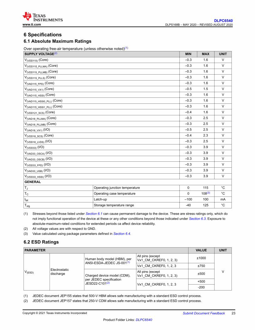
6 Specifications6.1 Absolute Maximum RatingsOver operating free-air temperature (unless otherwise noted)(1)
SUPPLY VOLTAGE(2) MIN MAX UNITV(VDD115) (Core) –0.3 1.6 V
V(VDD115_PLLMA) (Core) –0.3 1.6 V
V(VDD115_PLLMB) (Core) –0.3 1.6 V
V(VDD115_PLLS) (Core) –0.3 1.6 V
V(VAD115_FPD) (Core) –0.3 1.6 V
V(VAD115_VX1) (Core) –0.5 1.5 V
V(VAD115_HSSI) (Core) –0.3 1.6 V
V(VAD115_HSSI0_PLL) (Core) –0.3 1.6 V
V(VAD115_HSSI1_PLL) (Core) –0.3 1.6 V
V(VDD121_SCS) (Core) –0.4 1.6 V
V(VAD18_PLLMA) (Core) –0.3 2.5 V
V(VAD18_PLLMB) (Core) –0.3 2.5 V
V(VAD18_VX1) (I/O) –0.5 2.5 V
V(VDD18_SCS) (Core) –0.4 2.3 V
V(VDD18_LVDS) (I/O) –0.3 2.5 V
V(VDD33) (I/O) –0.3 3.9 V
V(VAD33_OSCA) (I/O) –0.3 3.9 V
V(VAD33_OSCB) (I/O) –0.3 3.9 V
V(VDD33_FPD) (I/O) –0.3 3.9 V
V(VAD33_USB) (I/O) –0.3 3.9 V
V(VDD33_HSSI) (I/O) –0.3 3.9 V
GENERALTJ Operating junction temperature 0 115 °C
TC Operating case temperature 0 108(3) °C
Ilat Latch-up –100 100 mA
Tstg Storage temperature range -40 125 °C
(1) Stresses beyond those listed under Section 6.1 can cause permanent damage to the device. These are stress ratings only, which donot imply functional operation of the device at these or any other conditions beyond those indicated under Section 6.3. Exposure toabsolute-maximum-rated conditions for extended periods ca affect device reliability.
(2) All voltage values are with respect to GND.(3) Value calculated using package parameters defined in Section 6.4.
6.2 ESD RatingsPARAMETER VALUE UNIT
V(ESD)Electrostaticdischarge
Human body model (HBM), perANSI-ESDA-JEDEC JS-001(1)
All pins (exceptVx1_CM_CKREF0, 1, 2, 3) ±1000
V
Vx1_CM_CKREF0, 1, 2, 3 ±750
Charged device model (CDM),per JEDEC specificationJESD22-C101(2)
All pins (exceptVx1_CM_CKREF0, 1, 2, 3) ±500
Vx1_CM_CKREF0, 1, 2, 3+500
-200
(1) JEDEC document JEP155 states that 500-V HBM allows safe manufacturing with a standard ESD control process.(2) JEDEC document JEP157 states that 250-V CDM allows safe manufacturing with a standard ESD control process.
www.ti.comDLPC6540
DLPS168B – MAY 2020 – REVISED AUGUST 2020
Copyright © 2021 Texas Instruments Incorporated Submit Document Feedback 23
Product Folder Links: DLPC6540

6.3 Recommended Operating ConditionsOver operating free-air temperature range (unless otherwise noted)PARAMETER TOLERANCE MIN NOM MAX UNITV(VDD115) (Core) 1.15-V Power ± 4.35% tolerance 1.10 1.15 1.20 V
V(VDD115_PLLMA) (Core) 1.15-V Digital Power -MCG-A PLL(Master ClockGenerator)
+4.35/-9.13%tolerance 1.045 1.15 1.20 V
V(VDD115_PLLMB) (Core) 1.15-V Digital Power -MCG-B PLL(Master ClockGenerator)
+4.35/-9.13%tolerance 1.045 1.15 1.20 V
V(VDD115_PLLS) (Core) 1.15-V Analog Power- SCG Doubler PLL
+4.35/-9.13%tolerance 1.045 1.15 1.20 V
V(VAD115_FPD) (Core) 1.15-V Analog Power- FPD
+4.35/-9.13%tolerance 1.045 1.15 1.20 V
V(VAD115_VX1) (Core) 1.15-V Analog Power- VX1
+4.35/-9.13%tolerance 1.045 1.15 1.20 V
V(VAD115_HSSI) (Core) 1.15-V Analog Power- HSSI
+4.35/-9.13%tolerance 1.045 1.15 1.20 V
ΔV(VAD115_HSSI) (Core) pk-pkVAD115_HSSIsupply noise @ 10MHz (sine)
20 mV
V(VAD115_HSSI0_PLL) (Core) 1.15-V Analog Power- HSSI0 PLL
+4.35/-9.13%tolerance 1.045 1.15 1.20 V
ΔV(VAD115_HSSI0_PLL) (Core) pk-pkVAD115_HSSI0_PLL supply noise @ 10MHz (sine)
20 mV
V(VAD115_HSSI1_PLL) (Core) 1.15-V Analog Power- HSSI1 PLL
+4.35/-9.13%tolerance 1.045 1.15 1.20 V
ΔV(VAD115_HSSI1_PLL) (Core) pk-pkVAD115_HSSI1_PLL supply noise @ 10MHz (sine)
20 mV
V(VDD121_SCS) (Core) 1.21V Digital Power -SCS DRAM
+7.43/-4.95%tolerance 1.15 1.21 1.30 V
V(VAD18_PLLMA) (Core) 1.8-V Analog Power -MCG-A PLL(Master ClockGenerator)
±5.0% tolerance 1.71 1.80 1.89 V
V(VAD18_PLLMB) (Core) 1.8-V Analog Power -MCG-B PLL(Master ClockGenerator)
±5.0% tolerance 1.71 1.80 1.89 V
V(VAD18_VX1) (I/O) 1.8-V Analog Power -VX1 Interface ±5.0% tolerance 1.71 1.80 1.89 V
V(VDD18_SCS) (Core) 1.8-V Digital Power -SCS DRAM ±5.0% tolerance 1.71 1.80 1.89 V
V(VDD18_LVDS) (I/O) 1.8-V Analog Power -DMD LS Interface ±5.0% tolerance 1.71 1.80 1.89 V
V(VDD33) (I/O) 3.3-V Digital Power- (All 3.3-V I/Owithout dedicated 3.3-V supply - e.g. GPIO)
±5.0% tolerance 3.135 3.3 3.465 V
DLPC6540DLPS168B – MAY 2020 – REVISED AUGUST 2020 www.ti.com
24 Submit Document Feedback Copyright © 2021 Texas Instruments Incorporated
Product Folder Links: DLPC6540

Over operating free-air temperature range (unless otherwise noted)PARAMETER TOLERANCE MIN NOM MAX UNITV(VAD33_OSCA) (I/O) 3.3-V Analog Power
- Crystal-OSCAInterface
±5.0% tolerance 3.135 3.3 3.465 V
V(VAD33_OSCB) (I/O) 3.3-V Analog Power- Crystal-OSCBInterface
±5.0% tolerance 3.135 3.3 3.465 V
V(VDD33_FPD) (I/O) 3.3-V Digital Power -FPD interface ±5.0% tolerance 3.135 3.3 3.465 V
V(VAD33_USB) (I/O) 3.3-V Analog Power -USB Interface ±5.0% tolerance 3.135 3.3 3.465 V
V(VDD33_HSSI) (I/O) 3.3-V Digital Power -DMD HSSI Interface ±5.0% tolerance 3.135 3.3 3.465 V
ΔV(VDD33_HSSI) (I/O) pk-pkVDD33_HSSIsupply noise @ 10MHz (sine)
60 mV
GENERAL
TJOperating junctiontemperature 0 115 °C
TCOperating casetemperature 0 108 °C
TAOperating ambienttemperature (1) (2) 0 55 °C
(1) The operating ambient temperature range values were determined based on the board design parameters described in Section10.1.1 , rather than using a JEDEC JESD51 standard test card and environment, along with min and max estimated power dissipationacross process, voltage, and temperature. Ambient thermal conditions, which impact RθJA, vary by application. Thus, maximumoperating ambient temperature varies by application.a. Ta_min = Tj_min – (Pd_min × RθJA) = 0°C – (host_min_valueW × host_value°C/W) = –host_calculated_value°Cb. Ta_max = Tj_max – (Pd_max × RθJA) = +115°C – (host_max_valueW × host_value°C/W) = +host_calculated_value°C
(2) Operating ambient temperature is dependent on system thermal design. Operating case temperature cannot exceed its specifiedrange across ambient temperature conditions.
www.ti.comDLPC6540
DLPS168B – MAY 2020 – REVISED AUGUST 2020
Copyright © 2021 Texas Instruments Incorporated Submit Document Feedback 25
Product Folder Links: DLPC6540

6.4 Thermal Information
THERMAL METRIC (1) TEST CONDITIONS (2)
ZDC
UNITP-HBGA676676 PINS (576
Populated)
RθJAJunction-to-air thermalresistance (3)
0 m/s of forced airflow, without heat-sink1 m/s of forced airflow, without heat-sink2 m/s of forced airflow, without heat-sink1 m/s of forced airflow, with heat-sink, 7 W2 m/s of forced airflow, with heat-sink, 7 W1 m/s of forced airflow, with heat-sink,15 W2 m/s of forced airflow, with heat-sink, 15 W
7.46.36.05.34.84.03.5
°C/W
RJCJunction-to-case thermalresistance (4) 2.7 °C/W
RJBJunction-to-board thermalresistance (4) 3.5 °C/W
ψJT (5)
Temperature variance fromjunction to package top centertemperature, per unit powerdissipation.
0 m/s of forced airflow, without heat-sink1 m/s of forced airflow, without heat-sink2 m/s of forced airflow, without heat-sink
0.60.60.6
°C/W
PMAX Package - Maximum Power(3) (6)0 m/s of forced airflow, without heat-sink1 m/s of forced airflow, without heat-sink2 m/s of forced airflow, without heat-sink
8.109.5210.00
W
(1) For more information about traditional and new thermal metrics, see the IC Package Thermal Metrics application report, SPRA953.(2) These test conditions also included a PCB sized at 101.3mm x 152.4mm incorporating the recommended PCB thermal enhancements
specified in Section 10.1.1. In addition, airflow is parallel to the board surface directed at the device.(3) See Table 6-1 for thermal parameters based on the example heat-sinks listed below
a. Heatsink-7 W: S1525-7W, Size = 25 mm x 25 mm x 7 mm, Pins = 7 x7 = 49 (Vendor: Alpha, Type S Series)b. Heatsink-15 W: S1530-15W, Size = 30 mm x 3 0mm x 15 mm, Pins = 8 x 8 = 64 (Vendor: Alpha, Type S Series)
(4) Due to the complex internal construction of the DLPC6540 controller, the RJC and RJB thermal coefficients do not always producean accurate junction temperature estimate. A limited set of comparison scenario data shows that the RJC and RJB modeled junctiontemperature can have a +9% to -2% error vs the actual temperature. The amount of this error varies with the use and size of anexternal heat sink as well as the amount of external air flow. Validate all thermal estimates based on RJC and RJB with an actualtemperature measurement at the top-center of the package plus the delta-temp defined by ψJT.
(5) Example: Using the power we expect of 11.31 W11.31 W * 0.6 °C/W = 6.786 °C = > TC-max = 115 °C - ~7 °C = 108 °C
(6) PMAX = (TJ-max - TA-max) / RθJA
Table 6-1. Thermal Examples using Two Different Heat-sinks
THERMAL METRIC (1) TEST CONDITIONSZDC
UNITP-HBGA676676 PINS (576 Populated)
RθJAJunction-to-air thermalresistance
1 m/s of forced airflow, with heat-sink, 7 W2 m/s of forced airflow, with heat-sink, 7 W1 m/s of forced airflow, with heat-sink, 15 W2 m/s of forced airflow, with heat-sink, 15 W
5.34.84.03.5
°C/W
PMAX Package - Maximum Power
1 m/s of forced airflow, with heat-sink, 7 W2 m/s of forced airflow, with heat-sink, 7 W1 m/s of forced airflow, with heat-sink, 15 W2 m/s of forced airflow, with heat-sink, 15 W
11.3212.5015.0017.14
W
(1) This table show examples of what is achievable based on the two example heat-sinks.
DLPC6540DLPS168B – MAY 2020 – REVISED AUGUST 2020 www.ti.com
26 Submit Document Feedback Copyright © 2021 Texas Instruments Incorporated
Product Folder Links: DLPC6540

6.5 Power Electrical CharacteristicsOver operating free-air temperature range (unless otherwise noted)
PARAMETER TEST CONDITIONS MIN TYP MAX(1) UNITV(VDD115) 1.15-V Power Maximum current at VDD115 = 1.2 V 5640 mA
V(VDD115_PLLMA) (Core) 1.15-V Digital PowerMCG-A PLL(Master Clock Generator)
Maximum current at VDD115_PLLMA =1.2 V 6 mA
V(VDD115_PLLMB) (Core) 1.15-V Digital PowerMCG-B PLL(Master Clock Generator)
Maximum current at VDD115_PLLMB =1.2 V 6 mA
V(VDD115_PLLS) (Core) 1.15-V Analog PowerSCG Doubler PLL
Maximum current at VDD115_PLLS =1.2 V 3 mA
V(VAD115_FPD) (Core) (2)1.15-V Analog PowerFPD
Maximum current at VAD115_FPD = 1.2VPorts A and B Active, Port C inactive
99 mA
V(VAD115_VX1) (Core) (2)1.15-V Analog PowerVX1
Maximum current at VAD115_VX1 = 1.2V8 Lanes, with total BW = 3.0Gbps)
400 mA
V(VAD115_HSSI) (Core) 1.15-V Digital PowerHSSI
Maximum current at VDD115_HSSI =1.2 VBoth ports active
462 mA
V(VAD115_HSSI0_PLL)(Core) 1.15-V Digital Power
HSSI0 PLL
Maximum current atVDD115_HSSI0_PLL = 1.2 VBoth ports active
1 mA
V(VAD115_HSSI1_PLL)(Core) 1.15-V Digital Power
HSSI1 PLL
Maximum current atVDD115_HSSI1_PLL = 1.2 VBoth ports active
1 mA
V(VDD121_SCS) (Core) 1.21V Digital PowerSCS DRAM
Maximum current at VDD121_SCS =1.30 V 334 mA
V(VAD18_PLLMA) (Core) 1.8-V Analog PowerMCG-A PLL(Master Clock Generator)
Maximum current at VAD18_PLLMA =1.89 V 10 mA
V(VAD18_PLLMB) (Core) 1.8-V Analog PowerMCG-B PLL(Master Clock Generator)
Maximum current at VAD18_PLLMB =1.89 V 10 mA
V(VAD18_VX1) (I/O) (2)1.8-V Analog PowerVX1 Interface
Maximum current at VAD18_VX1 = 1.89V8 Lanes, with total BW = 3.0Gbps
41 mA
V(VDD18_SCS) (Core) 1.8-V Digital PowerSCS DRAM
Maximum current at VDD18_SCS =1.89 V 327 mA
V(VDD18_LVDS) (I/O) 1.8-V Analog PowerDMD LS Interface
Maximum current at VDD18_LVDS =1.89 V 31 mA
V(VDD33) (I/O) 3.3-V Digital Power -(All 3.3-V I/O withoutdedicated 3.3-V supply -e.g. GPIO)
Maximum current at VDD33 = 1.3456 V 28 mA
V(VAD33_OSCA) (I/O) 3.3-V Analog PowerCrystal/OSCA Interface
Maximum current at VDD33_OSCA =1.3456 V 5 mA
V(VAD33_OSCB) (I/O) 3.3-V Analog PowerCrystal-OSCB Interface
Maximum current at VDD33_OSCB =1.3456 V 5 mA
V(VDD33_FPD) (I/O) (2)3.3-V Digital PowerFPD interface
Maximum current at VDD33_FPD =1.3456 VPorts A and B Active, Port C inactive
102 mA
V(VAD33_USB) (I/O) 3.3-V Analog PowerUSB Interface
Maximum current at VDD33_USB =1.3456 V 78 mA
www.ti.comDLPC6540
DLPS168B – MAY 2020 – REVISED AUGUST 2020
Copyright © 2021 Texas Instruments Incorporated Submit Document Feedback 27
Product Folder Links: DLPC6540

Over operating free-air temperature range (unless otherwise noted)PARAMETER TEST CONDITIONS MIN TYP MAX(1) UNIT
V(VDD33_HSSI) (I/O)3.3-V Digital PowerDMD HSSI Interface
Maximum current at VDD33_HSSI =1.3456 VBoth ports active, with total BW =3.0Gbps
194 mA
(1) Vendor estimate for worst case power PVT condition = corner process, high voltage, high temperature (115°C junction).(2) The V-by-One interface and FPD-Link receivers are never intended to be simultaneously enabled . Always disable one of these
interfaces.
DLPC6540DLPS168B – MAY 2020 – REVISED AUGUST 2020 www.ti.com
28 Submit Document Feedback Copyright © 2021 Texas Instruments Incorporated
Product Folder Links: DLPC6540

6.6 Pin Electrical CharacteristicsOver operating free-air temperature range (unless otherwise noted)(1)
PARAMETER TEST CONDITIONS MIN TYP MAX UNIT
VIHHigh-level inputthreshold voltage
1.8 V LVCMOS(I/O type 3 - LSDMD)
1.05
V
3.3 V OpenDrain(I/O type 4 - VX1) N/A
3.3 V LVCMOS(I/O type 6 - FPD)
0.8 ×VDD33_FPD
3.3 V LVCMOS(I/O type 6 - PP)
2.0
3.3 V LVCMOS(I/O type 8 - GPIO) 2.0
3.3 V LVCMOS(I/O type 9 - OSCA) 2.0
3.3 V LVCMOS(I/O type 10 -OSCB)
2.0
3.3 V OpenDrain(I/O type 13 - I2C) 0.7 × VDD33
VILLow-level inputthreshold voltage
1.8 V LVCMOS(I/O type 3 - LSDMD)
0.6
V
3.3 V OpenDrain(I/O type 4 - VX1) N/A
3.3 V LVCMOS(I/O type 6 - FPD) 0.2 × VDD33_FPD
3.3 V LVCMOS(I/O type 6 - PP)
0.8
3.3 V LVCMOS(I/O type 8 - GPIO) 0.8
3.3 V LVCMOS(I/O type 9 - OSCA) 0.8
3.3 V LVCMOS(I/O type 10 -OSCB)
0.8
3.3 V OpenDrain(I/O type 13 - I2C) 0.3 × VDD33
IIHHigh-level inputcurrent
1.8 V LVCMOS(I/O type 3 - LSDMD)
VIN = VAD18_LSIF –10 10
µA
3.3 V OpenDrain(I/O type 4 - VX1) N/A N/A
3.3 V LVCMOS(I/O type 6 - PP) -10 10
3.3 V LVCMOS(I/O type 8 - GPIO) VIN = VDD33 –10 10
3.3 V LVCMOS(I/O type 9 - OSCA) VIN = VDD33 –10 10
3.3 V LVCMOS(I/O type 10 -OSCB)
VIN = VDD33 –10 10
3.3 V OpenDrain(I/O type 13 - I2C) –10 10
www.ti.comDLPC6540
DLPS168B – MAY 2020 – REVISED AUGUST 2020
Copyright © 2021 Texas Instruments Incorporated Submit Document Feedback 29
Product Folder Links: DLPC6540

6.6 Pin Electrical Characteristics (continued)Over operating free-air temperature range (unless otherwise noted)(1)
PARAMETER TEST CONDITIONS MIN TYP MAX UNIT
IILLow-level inputcurrent
1.8 V LVCMOS(I/O type 3 - LSDMD)
VIN = VSS –10 10
µA
3.3 V OpenDrain(I/O type 4 - VX1) N/A N/A
3.3 V LVCMOS(I/O type 6 - PP) -10 10
3.3 V LVCMOS(I/O type 8 - GPIO) VIN = VSS –10 10
3.3 V LVCMOS(I/O type 9 - OSCA) VIN = VSS –10 10
3.3 V LVCMOS(I/O type 10 -OSCB)
VIN = VSS –10 10
3.3 V OpenDrain(I/O type 13 - I2C) –10 10
VOHHigh-level outputvoltage
1.8 V LVCMOS(I/O type 3 - LSDMD)
VDD18 - 0.6
V
3.3 V OpenDrain(I/O type 4 - VX1) N/A
3.3 V LVCMOS(I/O type 6 - PP) N/A
3.3 V LVCMOS(I/O type 8 - GPIO) IOH = 8 mA VDD33 - 0.6
3.3 V LVCMOS(I/O type 9 - OSCA) N/A
3.3 V LVCMOS(I/O type 10 -OSCB)
N/A
3.3 V OpenDrain(I/O type 13 - I2C) N/A
VOLLow-level outputvoltage
1.8 V LVCMOS(I/O type 3 - LSDMD)
0.4
V
3.3 V OpenDrain(I/O type 4 - VX1) IOL = 8 mA 0.4
3.3 V LVCMOS(I/O type 6 - PP) N/A
3.3 V LVCMOS(I/O type 8 - GPIO) IOL = 8 mA 0.4
3.3 V LVCMOS(I/O type 9 - OSCA) N/A
3.3 V LVCMOS(I/O type 10 -OSCB)
N/A
3.3 V OpenDrain(I/O type 13 - I2C) 3-mA sink 0.4
DLPC6540DLPS168B – MAY 2020 – REVISED AUGUST 2020 www.ti.com
30 Submit Document Feedback Copyright © 2021 Texas Instruments Incorporated
Product Folder Links: DLPC6540
6.6 Pin Electrical Characteristics (continued)Over operating free-air temperature range (unless otherwise noted)(1)
PARAMETER TEST CONDITIONS MIN TYP MAX UNIT
IOHHigh-level outputcurrent
1.8 V LVCMOS(I/O type 3 - LSDMD)
N/A
mA
3.3 V OpenDrain(I/O type 4 - VX1) N/A
3.3 V LVCMOS(I/O type 6 - PP) N/A
3.3 V LVCMOS(I/O type 8 - GPIO) VOH = VDD33 - 0.6 V 8
3.3 V LVCMOS(I/O type 9 - OSCA) N/A N/A
3.3 V LVCMOS(I/O type 10 -OSCB)
N/A N/A
3.3 V OpenDrain(I/O type 13 - I2C) N/A
IOLLow-level outputcurrent
1.8 V LVCMOS(I/O type 3 - LSDMD)
N/A
mA
3.3 V OpenDrain(I/O type 4 - VX1) VOL = 0.4 V 8
3.3 V LVCMOS(I/O type 6 - PP) N/A
3.3 V LVCMOS(I/O type 8 - GPIO) VOL = 0.4 V 8
3.3 V LVCMOS(I/O type 9 - OSCA) N/A N/A
3.3 V LVCMOS(I/O type 10 -OSCB)
N/A N/A
3.3 V OpenDrain(I/O type 13 - I2C) VOL = 0.6 V 6 -
IOZHigh-impedanceleakage current
1.8 V LVCMOS(I/O type 3 - LSDMD)
N/A
µA
3.3 V OpenDrain(I/O type 4 - VX1) -10 10
3.3 V LVCMOS(I/O type 6 - PP) -10 10
3.3 V LVCMOS(I/O type 8 - GPIO) VOUT = VDD33 –10 10
3.3 V LVCMOS(I/O type 9 - OSCA) N/A N/A
3.3 V LVCMOS(I/O type 10 -OSCB)
N/A N/A
3.3 V OpenDrain(I/O type 13 - I2C) N/A N/A
(1) The number inside each parenthesis for the I/O refers to the type defined in Table 5-13.
www.ti.comDLPC6540
DLPS168B – MAY 2020 – REVISED AUGUST 2020
Copyright © 2021 Texas Instruments Incorporated Submit Document Feedback 31
Product Folder Links: DLPC6540
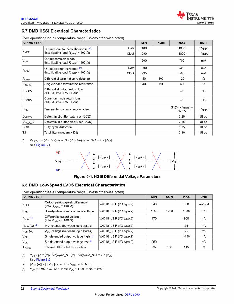
6.7 DMD HSSI Electrical CharacteristicsOver operating free-air temperature range (unless otherwise noted)PARAMETER MIN NOM MAX UNIT
VDIFFOutput Peak-to-Peak Differential (1)
(into floating load RLOAD = 100 Ω)Data 400 1000 mVppd
Clock 590 1000 mVppd
VCMOutput common mode(into floating load RLOAD = 100 Ω) 200 700 mV
|VOD| Output differential voltage(1)
(into floating load RLOAD = 100 Ω)Data 200 500 mV
Clock 295 500 mV
RDIFF Differential termination resistance 80 100 120 Ω
RTERM Single-ended termination resistance 40 50 60 Ω
SDD22 Differential output return loss(100 MHz to 0.75 × Baud) -8 dB
SCC22 Common mode return loss(100 MHz to 0.75 × Baud) -6 dB
NCM Transmitter common mode noise (7.5% × VDIFF) +25 mV mVppd
DJDATA Deterministic jitter data (non-DCD) 0.20 UI pp
DJCLOCK Deterministic jitter clock (non-DCD) 0.16 UI pp
DCD Duty cycle distortion 0.05 UI pp
TJ Total jitter (random + DJ) 0.30 UI pp
(1) VDIFF-pp = (Vp - Vn)cycle_N - (Vp - Vn)cycle_N+1 = 2 × |VOD|See Figure 6-1.
|VOD|
Vp
Vn
VCM
|VOD/2|
|VOD/2|
|VOD/2|
|VOD/2|
Figure 6-1. HSSI Differential Voltage Parameters
6.8 DMD Low-Speed LVDS Electrical CharacteristicsOver operating free-air temperature range (unless otherwise noted)PARAMETER MIN NOM MAX UNIT
VDIFFOutput peak-to-peak differential(into RLOAD = 100 Ω) VAD18_LSIF (I/O type 2) 340 600 mVppd
VCM Steady-state common mode voltage VAD18_LSIF (I/O type 2) 1100 1200 1300 mV
|VOD|(1) Differential output voltage(into RLOAD = 100 Ω) VAD18_LSIF (I/O type 2) 170 300 mV
|VOD (Δ) |(2) VOD change (between logic states) VAD18_LSIF (I/O type 2) 25 mV
VCM (Δ) VCM change (between logic states) VAD18_LSIF (I/O type 2) 25 mV
VOH Single-ended output voltage high (3) VAD18_LSIF (I/O type 2) 1450 mV
VOL Single-ended output voltage low (3) VAD18_LSIF (I/O type 2) 950 mV
Txterm Internal differential termination 85 100 115 Ω
(1) VDIFF-pp = (Vp - Vn)cycle_N - (Vp - Vn)cycle_N+1 = 2 × |VOD|See Figure 6-2
(2) |VOD (Δ)| = | | VOD|cycle _N - |VOD|cycle_N+1 |(3) VOH = 1300 + 300/2 = 1450; VOL = 1100- 300/2 = 950
DLPC6540DLPS168B – MAY 2020 – REVISED AUGUST 2020 www.ti.com
32 Submit Document Feedback Copyright © 2021 Texas Instruments Incorporated
Product Folder Links: DLPC6540

|VOD|
Vp
Vn
VCM
|VOD/2|
|VOD/2|
|VOD/2|
|VOD/2|
Figure 6-2. DMD Low-Speed Differential Voltage Parameters
6.9 V-by-One Interface Electrical CharacteristicsOver operating free-air temperature range (unless otherwise noted)PARAMETER(1) MIN NOM MAX UNITVDIFF Input peak-to-peak differential VAD18_VX1 (I/O type 1) 100 mVppd
|VID| Differential input voltage VAD18_VX1 (I/O type 1) 50 mV
Rxterm Internal differential termination VAD18_VX1 (I/O type 1) 80 100 120 Ω
(1) See the V-by-One interface standard for more information
6.10 USB Electrical Characteristics Over operating free-air temperature range (unless otherwise noted)PARAMETER(1) (2) MIN NOM MAX UNITLow-Speed and Full Speed (Input Level)
VIHSingle-ended input voltage high(driven) 2.0 V
VIHZSingle-ended input voltage high(floating) 2.7 3.6 V
VIL Single-ended input voltage low 0.8 V
VDI Differential input sensitivity |(DP) - (DM)| 0.2 V
VCM Differential common mode voltage Includes VDI range 0.8 2.5 V
Low-Speed and Full Speed (Output Level)
VOL Low-level output voltage with 1.425KΩ pullup to 3.6V 0.0 0.3 V
VOH High-level output voltage with 14.25KΩ pulldown 2.8 3.6 V
VCRS Output signal crossover voltage 1.3 2.0 V
High-Speed (Input Level)
VHSSQ
High-speed squelch detectionthreshold(differential signal amplitude)
100 150 mV
VHSDSC
High-speed disconnect detectionthreshold(differential signal amplitude)
525 626 mV
VHSCMHigh-speed data signal common modevoltage -50 500 mV
High-Speed (Output Level)
VHSOI High-speed idle level –10.0 10.0 mV
VHSOH High-speed data signal - high 360 440 mV
VHSOL High-speed data signal - low –10.0 10.0 mV
VCHIRPJHigh-speed chirp J level (differentialvoltage) 700 1100 mV
VCHIRPKHigh-speed chirp K level (differentialvoltage) -900 -500 mV
TerminationRPU Bus pullup resistor 1.425 1.575 KΩ
RPD Bus pulldown resistor 14.25 15.75 KΩ
www.ti.comDLPC6540
DLPS168B – MAY 2020 – REVISED AUGUST 2020
Copyright © 2021 Texas Instruments Incorporated Submit Document Feedback 33
Product Folder Links: DLPC6540

Over operating free-air temperature range (unless otherwise noted)PARAMETER(1) (2) MIN NOM MAX UNITZHSDRV High-speed driver output impedance 40.5 49.5 Ω
(1) Referenced to VAD33_USB (I/O type 11)(2) When used as a master as part of USB OTG, the DLPC6540 requires an External USB Switch to provide the USB 5-V power. The
example shown in Figure 6-3 makes use of a TI TPS2500/2501 device. The example figure does not describe the required ancillarycomponents (such as, resistors and capacitors). For this information please refer to the USB Switch logic datasheet for the selecteddevice. The External USB Switch is not required for product configurations that are supporting USB slave mode only.
USB Power Switch
w/ Boost
Converter
(TPS2500 or TPS2501)
Micro
AB
Receptable
GND
ID
D+
D±
VBUS
USB_ID
USB_DAT_P
USB_VBUS
USB_DAT_N
USB
IN
1.8 V to 5.25 V
ENUSB
GPIO_48
EN
Controller
Figure 6-3. External USB Switch Example for DLPC6540 Controller as USB OTG Master
DLPC6540DLPS168B – MAY 2020 – REVISED AUGUST 2020 www.ti.com
34 Submit Document Feedback Copyright © 2021 Texas Instruments Incorporated
Product Folder Links: DLPC6540

6.11 System Oscillator Timing RequirementsPARAMETER MIN NOM MAX UNITƒclock Clock frequency, REFCLKA(1) (2) PLLA: 40 MHz 39.9960 40.000 40.0040 MHz
tc Cycle time, REFCLKA(1) PLLA: 40 MHz 24.9975 25.000 25.0025 ns
tw(H) Pulse duration(3), REFCLKA, high PLLA: 40 MHz50% to 50% reference points (signal) 11.25 ns
tw(L) Pulse duration(3), REFCLKA, low PLLA: 40 MHz50% to 50% reference points (signal) 11.25 ns
tt Transition time(3), REFCLKA, tt = tƒ / trPLLA: 40 MHz20% to 80% reference points (signal) 2.5 ns
tjp
Long term periodic jitter(3), REFCLKA(that is the deviation in period fromideal period due solely to highfrequency jitter)
PLLA: 40 MHz 18 ps
fclock Clock frequency, REFCLKB(1) PLLB: 38 MHz 37.9962 38.000 38.0038 MHz
tc Cycle time, REFCLKB(1) PLLB: 38 MHz 26.3132 26.3157 26.3184 ns
tw(H) Pulse duration(3), REFCLKB, high PLLB: 38 MHz50% to 50% reference points (signal) 11.84 ns
tw(L) Pulse duration(3), REFCLKB, low PLLB: 38 MHz50% to 50% reference points (signal) 11.84 ns
tt Transition time(3), REFCLKB, tt = tƒ / trPLLB: 38 MHz20% to 80% reference points (signal) 2.63 ns
tjp
Long term periodic jitter(3), REFCLKB(that is the deviation in period fromideal period due solely to highfrequency jitter)
PLLB: 38 MHz 18 ps
(1) The REFCLK inputs do not support spread spectrum clock spreading.(2) Multi-Controller systems require that a single oscillator be used to drive the REFCLKA input for all controllers in the system.(3) Applies only when driven through an external digital oscillator. This is a 1 sigma RMS value.
REFCLK 50%
80%
20%50%
50%
tc
tw(H) tw(L)
tt
80%
20%
tt
Figure 6-4. System Oscillators
www.ti.comDLPC6540
DLPS168B – MAY 2020 – REVISED AUGUST 2020
Copyright © 2021 Texas Instruments Incorporated Submit Document Feedback 35
Product Folder Links: DLPC6540

6.12 Power Supply and Reset Timing RequirementsPARAMETER MIN MAX UNIT
tRAMP-UPPower supply ramp-up time.(1) Figure 6-5
Power supply ramp for each supplyRamp-up time: TOV × 10% to TOV × 90%TOV = Typical Operational Voltage
0.01 10 ms
tRAMP-UP-TOTALTotal power supply ramp-uptime.(1)
Total time within which the 1.15-V, 1.8-V, 1.21-V,and 3.3-V supplies must complete their ramp-upfrom the start of the 1.15-V ramp-up.Ramp-up time: TOV × 10% to TOV × 90%TOV = Typical Operational Voltage
100 ms
tRAMP-DOWNPower supply ramp-downtime. (1) Figure 6-5 Figure 6-6
Power supply ramp for each supplyRamp-down time: TOV × 90% to TOV × 10%TOV = Typical Operational Voltage
0 100 ms
tRAMP-DOWN-TOTAL Total power supply ramp-down time.(1)
Total time within which the 1.15-V, 1.8-V, 1.21-V, and 3.3-V supplies must complete their ramp-down from the start of the 3.3-V ramp-up.Ramp-down time: TOV × 90% to TOV × 10%TOV = Typical Operational Voltage
100 ms
tRUSD181.8-V Supply Ramp-up StartDelay (2) Figure 6-6
Delay from 1.15-V supply ramp start to 1.8-Vsupply ramp start. See (3) ms
tRUSD333.3-V Supply Ramp-up StartDelay (2) Figure 6-6
Delay from 1.15-V supply ramp start to 3.3-Vsupply ramp start 10 50 ms
tRUSD121.21-V Supply Ramp-up StartDelay (2) Figure 6-6
Delay from 1.8-V supply ramp start to 1.21-Vsupply ramp start. See (4) ms
tRDSD181.8-V Supply Ramp-downStart Delay (2) Figure 6-6
Delay from 1.21-V supply ramp start to 1.8-Vsupply ramp start. See (5) ms
tRDSD115 1.15-V Supply Ramp-downStart Delay (2) Figure 6-6
Delay from 3.3-V supply ramp start to 1.15-Vsupply ramp start.
See
tEWEarly Warning Time Figure6-8
PWRGOOD goes inactive low (as an earlywarning) prior to any power supply voltage goingbelow the controller specification
500 µs
tPH Power Hold Time Figure 6-8 POSENSE remains active after PWRGOOD isdisabled 500 µs
tw1Pulse duration, in-active low,PWRGOOD Figure 6-7
PWRGOOD inactive time while POSENSE isactive50% to 50% reference points (signal)
4 1000 (6) µs
tt1Transition time, PWRGOODtt1 = tƒ1 and tr1Figure 6-7
Rise and Fall time for PWRGOOD20% to 80% reference points (signal) 625 µs
tw2Pulse duration, in-active low,POSENSE Figure 6-8
POSENCE inactive time while PWRGOOD isinactive50% to 50% reference points (signal)
100 ms
tt2Transition time, POSENSEtt1 = tƒ1 and tr1Figure 6-8
Rise and Fall time for POSENSE (7)
20% to 80% reference points (signal) 25 µs
tPSDPWRGOOD Start DelayFigure 6-7
Time after rising edge of POSENSE beforePWRGOOD effects DLPC6540 operation 51.5 60 ms
tPROJ_ON PROJ_ON fall time delay toPWRGOOD Figure 6-8
Fall DelayPROJ_ON 80% to PWRGOOD 80% fall timestart
10 ms
tREFCLKA Time to stable REFCLKAFigure 6-7
Time to stable REFLCKA before POSENSE See
(1) It is assumed that all 1.15-V supplies come from the same source, although some can have additional filtering before entering theDLPC6540. As such, it is expected these supplies to ramp together (aside from differences caused by filtering). This same expectationis true for the 1.21-V, 1.8-V, and 3.3-V supplies.
(2) The DLPC6540 has specific power supply sequencing requirements which are listed below, and which also include the timingsspecified in this table.
DLPC6540DLPS168B – MAY 2020 – REVISED AUGUST 2020 www.ti.com
36 Submit Document Feedback Copyright © 2021 Texas Instruments Incorporated
Product Folder Links: DLPC6540

a. Power Up Order:i. 1.15-V (Core, Analog) » 1.8-V (I/O, SCS) » 1.21-V (SCS)ii. 1.15-V (Core, Analog) » 3.3-V (I/O
b. Power Down Order:i. 3.3-V (I/O) » 1.15-V (Core, Analog)ii. 1.21-V (SCS) » 1.8-V (I/O, SCS) » 1.15-V (Core, Analog)
(3) This delay requirement parameter is defined as the time between two events. The first event is the point where the 1.15-V powersupply ramp-up is started, and the second event is when the 1.15-V supply ramp-up reaches 80% of TOV (at which point the 1.8-Vsupply can start its ramp-up). Because the occurrence of the second event depends on the specific design of the 1.15-V power supply,the designer must determine the specific delay time.
(4) This delay requirement parameter is defined as the time between two events. The first event is the point where the 1.8-V power supplyramp-up is started, and the second event is when the 1.8-V supply ramp-up reaches 80% of TOV (at which point the 1.21-V supply canstart its ramp-up). Because the occurrence of the second event depends on the specific design of the 1.8-V power supply, the designermust determine the specific delay time.
(5) This delay requirement parameter is defined as the time between two events. The first event is the point where the 1.21-V powersupply ramp-down is started, and the second event is when the 1.21-V supply ramp-down reaches 20% of TOV (at which point the1.8-V supply can start its ramp-down). Because the occurrence of the second event depends on the specific design of the 1.21-Vpower supply, the designer must determine the specific delay time.
(6) This max value is only applicable if the 1.8-V power remains ON while PWRGOOD is inactive. Otherwise, there is no maximum limit.(7) As long as noise on this signal is below the hysteresis threshold
tRAMP-UP
10%
90%TOV
tRAMP-DOWN
10%
90%
Figure 6-5. Power Supply Ramp Time
tRUSD18
1.15V (Core/Analog)
1.21V (SCS)
1.8V (I/O, SCS)
3.3V (I/O)
tRUSD33
tRUSD12
tRDSD18
tRAMP-DOWN
80%
80%
20%
Figure 6-6. Power Supply Ramp Sequencing Profiles
www.ti.comDLPC6540
DLPS168B – MAY 2020 – REVISED AUGUST 2020
Copyright © 2021 Texas Instruments Incorporated Submit Document Feedback 37
Product Folder Links: DLPC6540

POSENSE
DC Power
Supplies
PWRGOOD
tt2
tt1tt1
80%
20%
80%
20%20%
50% 50%
tW1
80%
tPSD
tREFCLKA
Figure 6-7. Power Up Timing
POSENSE
DC Power
Supplies
PWRGOOD
tt2tt2
80%
20%20%
50% 50%
tW2
80%
tEW
tt1
80%
20%
tPH
PROJ_ON
(If applicable)
tPROJ_ON
80%
20%
Figure 6-8. Power Down Timing
DLPC6540DLPS168B – MAY 2020 – REVISED AUGUST 2020 www.ti.com
38 Submit Document Feedback Copyright © 2021 Texas Instruments Incorporated
Product Folder Links: DLPC6540

6.13 DMD HSSI Timing Requirementsover operating free-air temperature range (unless otherwise noted)PARAMETER MIN NOM MAX UNITBaud Baud Rate 2.4 3.2 Gbps
UI Unit Interval, 1/Baud 312.5 416.7 ps
tRDifferential output rise time (1)
(0% to 100% of minimum eye mask height)Data 50 115 ps
Clock 50 135 ps
tFDifferential output fall time (1)
(0% to 100% of minimum eye mask height)Data 50 115 ps
Clock 50 135 ps
tX1 maximum eye closure at zero crossing 0.15 UI
tX2 maximum eye closure at minimum eye height 0.375 UI
tEYE Differential Data Eye 0.7 UI
tskln2ln Lane to lane skew within a macro |200| ps
tskM2M Lane to lane skew macro to macro |4UI+200| ps
fSSCD Spread Spectrum (Down Spreading Only) (2) When SSCD Enabled 1 %
fMOD Modulation Frequency (2) When SSCD Enabled 78.125 KHz
(1) Rise and Fall times are associated with VDIFF-pp as shown in Figure 6-9(2) When SSCD is enabled, the available modulation waveform is: Triangular
+VDIFF(PP)/2
Diffe
ren
tia
l V
olta
ge
(%
)
20
10
40
30
60
(0 V) 50
80
70
100
90
0
tF. tR.
VDIFF(PP)
±VDIFF(PP)/2
VOD(min)
±VOD(min)
VCM is removed when signals are viewed differentially
Figure 6-9. HSSI Differential Timing Parameters
6.14 DMD Low-Speed LVDS Timing Requirementsover operating free-air temperature range (unless otherwise noted)PARAMETER MIN NOM MAX UNITfclock 119.966 120 120.034 MHz
tR (1) Differential output rise time(10% to 90%) 250 ps
tF (1) Differential output fall time(10% to 90%) 250 ps
DCD Duty Cycle Distortion 45 55 %
(1) Rise and Fall times are associated with VDIFF-pp as shown in Figure 6-10
www.ti.comDLPC6540
DLPS168B – MAY 2020 – REVISED AUGUST 2020
Copyright © 2021 Texas Instruments Incorporated Submit Document Feedback 39
Product Folder Links: DLPC6540

+VDIFF(PP)/2
Diffe
ren
tia
l V
olta
ge
(%
)
20
10
40
30
60
(0 V) 50
80
70
100
90
0
tF .
VDIFF(PP)
±VDIFF(PP)/2
tR.
VCM is removed when signals are viewed differentially
Figure 6-10. DMD Low-Speed Differential Timing Parameters
6.15 V-by-One Interface General Timing Requirements PARAMETER(1) MIN MAX UNIT
fclock Source clock frequency40 (1 lane)
20 (1 lane with PixelRepeat) (2)
600 (8lanes) MHz
flink-ck Link clock frequency per lane (3)
8 lanes4 lanes2 lanes1 lane
434343
43 (21.5 with PixelRepeat)
75858585
MHz
flink Link transfer rate (3)3-Byte Mode4-Byte Mode5-Byte Mode
22
2.15
2.553.03.0
Gbps
tRBIT Unit interval3-Byte Mode4-Byte Mode5-Byte Mode
392294294
500500500
pspsps
tA Jitter Margin 0.25 UI
tB Rise / Fall Time 0.05 UI
tEYE Differential Data Eye 0.5 UI
tskew_intra Allowable intra-pair skew 0.3 5- UI
tskew_inter Allowable Inter-pair Skew 5 UI
foskew_inter Allowable Inter-pair frequency offset –300 300 ppm
Tj Total jitter - 0.5 UI
Rj Random jitter 10^12 UI - 0.2 UI
Dj_ISI Deterministic jitter (ISI) - 0.2 UI
Sj Sinusoidal jitter - 0.1 UI
(1) V-by-One high-speed technology supports 1, 2, 4 or 8 lane operation, in addition to 3-Byte, 4-Byte, and 5-Byte transfer modes(2) Pixel repeat is a method used to support slower clock rate sources, whereby, the source come at twice the original clock rate, with
each data pixel being repeated once, and blanking being doubled as well. This method must operate external to DLPC6540. Oncereceived, the DLPC6540 discards each duplicate data pixel and blanking clock. Pixel repeat is supported only during 1- lane operation.
(3) For V-by-One high-speed technology, both link clock rate and link transfer rate limits must be met for any source.
DLPC6540DLPS168B – MAY 2020 – REVISED AUGUST 2020 www.ti.com
40 Submit Document Feedback Copyright © 2021 Texas Instruments Incorporated
Product Folder Links: DLPC6540

6.16 Source Frame Timing RequirementsSee Figure 6-11PARAMETER (1) MIN MAX UNIT
tp_vsw VSYNC Active Pulse Width 50% referencepoints 1 127 lines
tp_vbp Vertical back porch (VBP) (2) 50% referencepoints 2 (3) lines
tp_vƒp Vertical front porch (VFP) (2) 50% referencepoints MAX[ (TVBMIN - 65 ), 1] (3) lines
tp_tvb Total vertical blanking (TVB) (2) 50% referencepoints See (4) lines
tp_hsw HSYNC Active Pulse Width 50% referencepoints 16 PCLKs
tp_hbp Horizontal back porch (HBP) (5) 50% referencepoints
5 (Digital Video Sources)65 (Analog Video Sources) PCLKs
tp_hfp Horizontal front porch (HFP) (5) 50% referencepoints 2 PCLKs
tp_thb Total horizontal blanking (THB) (5) 50% referencepoints
20 (Digital Video Sources)80 (Analog Video Sources) (6) PCLKs
fline Horizontal line rate 37.354 K Hz
APPL Active Pixels per Line 640 4096 Pixels
ALPF Active Lines per Frame 480 2160 (Normal) Lines
(1) The requirements in the table apply to all external sources(2) Vertical Blanking Parameter Definitions:
a. Vertical Back Porch: Time from the leading edge of VSYNC to the leading edge of HSYNC for the first active line, and includes theVSYNC pulse width tp_vsw.
b. Vertical Front Porch: Time from the leading edge of HSYNC following the last active line in a frame to the leading edge of VSYNCc. Total Vertical Blanking: The sum of VBP + VFP = TVB.
(3) The vertical blanking required (per TVB) can be allocated as desired as long as the VFP and VBP minimum values are met.(4) The minimum TVB can be calculated using the following:
TVBmin = 11 + ROUNDUP(LLS_VFP_MIN × (Source_ALPF/VPS_ALPF)), where:a. LLS_VFP_MIN (Normal Mode) = 22b. Source_ALPF = Active Lines Per Frame of the incoming sourcec. VPS_ALPF = 1080 (for 1920x1080 Native products and 3840x2160 4-way XPR products)d. Less TVBmin blanking can be required depending on the video processing being done. The configurations that drive the worst
case minimum value are those configurations that combine the maximum (or near maximum) capabilities of functions such asscaling, warping, and keystone correction.
e. This is applicable to all sources (Section 7.4). Other sources require directed testing in the end application.f. The minimum recommended TVB with CVT 1.2 sources is 23.
(5) Horizontal Blanking Parameter Definitions:a. Horizontal Back Porch: Time from the leading edge of HSYNC to the rising edge of DATEN, and includes the HSYNC pulse width
tp_hsw.b. Horizontal Front Porch: Time from the falling edge of DATEN to the leading edge of HSYNC.c. Total Horizontal Blanking: The sum of HBP + HFP = THB.
(6) The horizontal blanking required (per THB) can be allocated as desired as long as the HFP and HBP minimum values are met.
www.ti.comDLPC6540
DLPS168B – MAY 2020 – REVISED AUGUST 2020
Copyright © 2021 Texas Instruments Incorporated Submit Document Feedback 41
Product Folder Links: DLPC6540

VSYNC_WE
HSYNC_CS
DATAEN_CMD
tp_vsw
1 Frame
tp_vbp tp_vfp
HSYNC_CS
DATAEN_CMD
tp_hsw
1 Line
tp_hfptp_hbp
PDATA(23/15:0) P0
PCLK
P1 P2 P3P
n-2
P
n-1Pn
(This diagram assumes the VSYNC
active edge is the rising edge)
(This diagram assumes the HSYNC
active edge is the rising edge)
Figure 6-11. Source Frame Timing
6.17 Synchronous Serial Port Interface Timing RequirementsFor SSP0, SSP1 and SSP2(1)(2)
PARAMETER MIN MAX UNITSSP Masterfclock Clock frequency, SSPx_CLK 50% to 50% reference points 0.38 39.0 MHz
tclock Clock Period, SSPx_CLK 50% to 50% reference points 25.6 3632 ns
tw(L) Pulse duration low, SSPx_CLK 50% to 50% reference points 12.0 ns
tw(H) Pulse duration high, SSPx_CLK 50% to 50% reference points 12.0 ns
tdelay Output Delay – SSPx_TXD (MOSI) -2.5 2.5 ns
tsu Setup time – SSPx_RXD (MISO) 50% to 50% reference points 15.0 ns
th hold time – SSPx_RXD (MISO) 50% to 50% reference points 0 ns
tt Transition time (tr and tf- SSPx_RXD 20% to 80% reference points 1.5 ns
tclkjit Clock Jitter, SSPx_CLK 300 ps
tdelay∆ Clock output delay ∆ | tw(H) - tw(L) | 500 ps
SSP Slavetdelay Output Delay – SSPx_TXD (MOSI) 0 15 ns
tsu Setup time – SSPx_RXD (MISO) 50% to 50% reference points 2.5 ns
th hold time – SSPx_RXD (MISO) 50% to 50% reference points 2.5 ns
(1) The DLPC6540 SPI interfaces support SPI Modes 0, 1, 2, and 3 (that is, both clock polarities and both clock phases) as shown inTable 6-2 and Figure 6-12. As such, each SPI interface configuration must be setup to match the SPI mode being used.
(2) In most SPI applications, one clock edge is used by both master and slave devices for transmitting data while the other edge is useby both for sampling received data. This is referred to as Standard SPI Protocol. To maximize the SPI_CLK frequency potential, SPImasters can alternatively be designed to sample the data in (MISO) bit on the same clock edge used to transmit the next data out(MOSI) bit. This is referred to as Enhanced SPI Protocol. The DLPC6540 SPI master implementation supports both protocols (part
DLPC6540DLPS168B – MAY 2020 – REVISED AUGUST 2020 www.ti.com
42 Submit Document Feedback Copyright © 2021 Texas Instruments Incorporated
Product Folder Links: DLPC6540
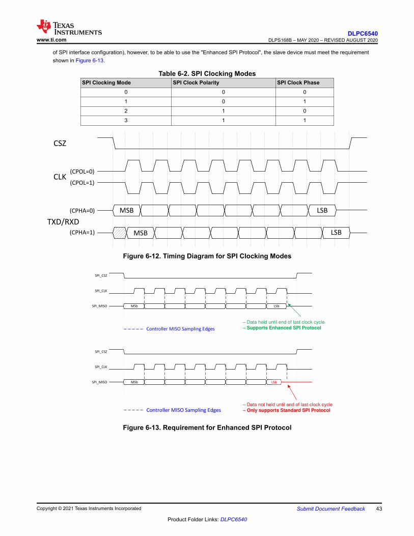
of SPI interface configuration), however, to be able to use the "Enhanced SPI Protocol", the slave device must meet the requirementshown in Figure 6-13.
Table 6-2. SPI Clocking ModesSPI Clocking Mode SPI Clock Polarity SPI Clock Phase
0 0 0
1 0 1
2 1 0
3 1 1
MSB
MSB
LSB
LSB(CPHA=1)
(CPHA=0)
(CPOL=1)
(CPOL=0)CLK
TXD/RXD
CSZ
Figure 6-12. Timing Diagram for SPI Clocking Modes
SPI_CLK
SPI_CSZ
SPI_MISO MSb LSb
± Data held until end of last clock cycle
± Supports Enhanced SPI Protocol
SPI_CLK
SPI_CSZ
SPI_MISO MSb LSb
Controller MISO Sampling Edges± Data not held until end of last clock cycle
± Only supports Standard SPI Protocol
Controller MISO Sampling Edges
Figure 6-13. Requirement for Enhanced SPI Protocol
www.ti.comDLPC6540
DLPS168B – MAY 2020 – REVISED AUGUST 2020
Copyright © 2021 Texas Instruments Incorporated Submit Document Feedback 43
Product Folder Links: DLPC6540

tclock
tw(H) tw(L)
50%50%50%
Valid
tsu th
SSPx_CLK
(Controller output)
SSPx_TXD
(Controller output)
ValidSSPx_RXD
(Controller input)
tt
80%
20%50%
ValidValid
Valid
tdelay(min)tdelay(max)
SSPx_RXD
(Controller input)
Figure 6-14. Timing Diagram for SSP Master (Modes 0/3)
DLPC6540DLPS168B – MAY 2020 – REVISED AUGUST 2020 www.ti.com
44 Submit Document Feedback Copyright © 2021 Texas Instruments Incorporated
Product Folder Links: DLPC6540

6.18 Master and Slave I2C Interface Timing RequirementsFor IIC0, IIC1 and IIC2PARAMETER(1) MIN MAX UNITfclock Clock frequency, IICx_SCL (2)
(50% reference points)Full speed 400 kHz
Standard mode 100 kHz
CL Capacitive Load (for each bus line) 200 pF
(1) Meets all I2C timing per the I2C Bus Specification (except for capacitive loading as specified). For reference see Version 2.1 of thePhillips-NXP specification.
(2) By definition, I2C transactions operate at the speed of the slowest device on the bus. Full Speed operation requires all other I2Cdevices on the bus support Full Speed operation. The length of the line (due to its capacitance), as well as the value of the I2C pullupresistors can reduce the obtainable clock rate.
6.19 Programmable Output Clock Timing RequirementsPARAMETER MIN MAX UNITfclock Clock frequency, OCLKA (1) 0.19 48.75 MHz
tclock Clock period, OCLKA 20.52 5263.15 ns
tw(H) Pulse duration high, OCLKA(50% reference points)
(tclock/2) - 2 ns
tw(L) Pulse duration low, OCLKA(50% reference points)
(tclock/2) - 2 ns
tcclkjit Jitter, OCLKA 200 ps
fclock Clock frequency, OCLKB (1) 0.19 48.75 MHz
tclock Clock period, OCLKB 20.52 5263.15 ns
tw(H) Pulse duration high, OCLKB(50% reference points)
(tclock/2) - 2 ns
tw(L) Pulse duration low, OCLKB(50% reference points)
(tclock/2) - 2 ns
tcclkjit Jitter, OCLKB 200 ps
fclock Clock frequency, OCLKC (1) 0.19 48.75 MHz
tclock Clock period, OCLKC 20.52 5263.15 ns
tw(H) Pulse duration high, OCLKC(50% reference points)
(tclock/2) - 2 ns
tw(L) Pulse duration low, OCLKC(50% reference points)
(tclock/2) - 2 ns
tcclkjit Jitter, OCLKC 200 ps
fclock Clock frequency, OCLKD (1) 0.19 48.75 MHz
tclock Clock period, OCLKD 20.52 5263.15 ns
tw(H) Pulse duration high, OCLKD(50% reference points)
(tclock/2) - 2 ns
tw(L) Pulse duration low, OCLKD(50% reference points)
(tclock/2) - 2 ns
tcclkjit Jitter, OCLKD 200 ps
(1) a. OCLKA is a dedicated pin, while OCLKB thru OCLKD are available via GPIO as alternate functions.b. The frequency of OCLKA thru OCLKD is programmable, with each having a power-up default frequency of 0.77 MHz. This default
frequency is not that meaningful for OCLKB thru OCLKD since they must be configured to their alternate GPIO function beforethey can be used as a clock output.
www.ti.comDLPC6540
DLPS168B – MAY 2020 – REVISED AUGUST 2020
Copyright © 2021 Texas Instruments Incorporated Submit Document Feedback 45
Product Folder Links: DLPC6540

6.20 JTAG Boundary Scan Interface Timing Requirements (Debug Only)See Figure 6-15PARAMETER MIN MAX UNITƒclock Clock frequency, TCK 20 MHz
tclock Clock period, TCK 50 ns
tw(H) Pulse duration low, TCK 50% reference points 23 ns
tw(L) Pulse duration high, TCK 50% reference points 27 ns
ts Setup time – TDI valid before TCK↑ 50% reference points 10 ns
th Hold time – TDI valid after TCK↑ 50% reference points 10 ns
ts Setup time – TMS1 valid before TCK↑ 50% reference points 10 ns
th Hold time – TMS1 valid after TCK↑ 50% reference points 10 ns
tt Transition time (tr and tf 20% to 80% reference points 3 ns
tdelay Output delay, TCK↓ to TDO1 60pF load 0 15 ns
tclock
tw(H) tw(L)
50%50%50%
Valid
tsu th
TCK
(Controller input)
TDI / TMS1
(Controller input)
TDO1
(Controller output)
tt
80%
20%
tdelay
Valid
50%
50%
Figure 6-15. Timing Diagram for JTAG Boundary Scan
DLPC6540DLPS168B – MAY 2020 – REVISED AUGUST 2020 www.ti.com
46 Submit Document Feedback Copyright © 2021 Texas Instruments Incorporated
Product Folder Links: DLPC6540

6.21 JTAG ARM Multi-Ice Interface Timing Requirements (Debug Only)See Figure 6-16PARAMETER MIN MAX UNITƒclock Clock frequency, TCK 8.33 MHz
tclock Clock period, TCK 120 ns
tw(H) Pulse duration low, TCK 50% reference points 50 ns
tw(L) Pulse duration high, TCK 50% reference points 50 ns
ts Setup time – TDI valid before TCK↑ 50% reference points 15 ns
th Hold time – TDI valid after TCK↑ 50% reference points 15 ns
ts Setup time – TMS2 valid before TCK↑ 50% reference points 15 ns
th Hold time – TMS2 valid after TCK↑ 50% reference points 15 ns
tt Transition time (tr and tf 20% to 80% reference points 5 ns
tdelay Output delay, TCK↓ to TDO2 0 15 ps
tclock
tw(H) tw(L)
50%50%50%
Valid
tsu th
TCK
(Controller input)
TDI / TMS2
(Controller input)
ValidTDO2
(Controller output)
tt
80%
20%
tdelay
50%
50%
Figure 6-16. Timing Diagram for JTAG ARM Multi-Ice
www.ti.comDLPC6540
DLPS168B – MAY 2020 – REVISED AUGUST 2020
Copyright © 2021 Texas Instruments Incorporated Submit Document Feedback 47
Product Folder Links: DLPC6540
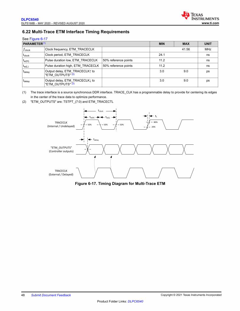
6.22 Multi-Trace ETM Interface Timing RequirementsSee Figure 6-17PARAMETER(1) MIN MAX UNITƒclock Clock frequency, ETM_TRACECLK 41.56 MHz
tclock Clock period, ETM_TRACECLK 24.1 ns
tw(H) Pulse duration low, ETM_TRACECLK 50% reference points 11.2 ns
tw(L) Pulse duration high, ETM_TRACECLK 50% reference points 11.2 ns
tdelay Output delay, ETM_TRACECLK↑ to"ETM_OUTPUTS" (2)
3.0 9.0 ps
tdelay Output delay, ETM_TRACECLK↓ to"ETM_OUTPUTS" (2)
3.0 9.0 ps
(1) The trace interface is a source synchronous DDR interface. TRACE_CLK has a programmable delay to provide for centering its edgesin the center of the trace data to optimize performance.
(2) "ETM_OUTPUTS" are: TSTPT_(7:0) and ETM_TRACECTL
tclock
tw(H) tw(L)
50%50%50%TRACECLK
(Internal / Undelayed)
^dD_KhdWhd^_
(Controller outputs)
tt
80%
20%
tdelay
TRACECLK
(External / Delayed)
Figure 6-17. Timing Diagram for Multi-Trace ETM
DLPC6540DLPS168B – MAY 2020 – REVISED AUGUST 2020 www.ti.com
48 Submit Document Feedback Copyright © 2021 Texas Instruments Incorporated
Product Folder Links: DLPC6540

7 Detailed Description7.1 OverviewThe DLP® Products chipset consists of three components – the DLP471TP, the DLPC6540, and the DLPA3005 .The DLPC6540 is the display controller for the DMD - it formats incoming video and controls the timing of theDMD. It also controls DLPA3005 light source signal timing to coordinate with DMD timing in order to synchronizelight output with DMD mirror movement. The DLPC6540 provides interfaces such as V-by-One and HSSI (DMDinterface) to minimize power consumption and EMI. Applications include mobile smart tv, digital signage, andmobile home cinema.
7.2 Functional Block Diagram
DLPC6540
Master
DLPA3005
TI DLP chipset
Third party component
VBIAS, VOFFSET, VRESET
SYSPWR (14.5 V to 20 V)
PWRGOOD
LS Interface
PROJ_ON
I2C
I2C BUSY
Vx1
2-Port HSSI
GPIO (PROJ_ON)
GPIO
SPI BUS (Ctrl) (4)
POSENSE
Front End
Device
Vx1:
3840 × 2160
@ 60Hz
USB Mux
DC
SupplyVSPI1.8 V
1.1
Reg
1.1 V @ 3 A
L3
LDO 2
LED_SEL (2)
1.8
Reg
USB Camera
Actuator
Driver
4-Position
Actuator
Flash (2)
(23) (18)ADDR DATA
3D L/R
Fan or
programmable DC supply
RESETZ
INITZ
DC
Reg
L4
L5
1.8 V @ 3 A for
DMD and DLPC6540
LDO 1 3.3 V @ 2 A2.5 V
DLPC471TP
.47 4K UHD DMD
VLED
L1
RLIM current sense
SYSPWR
L2
(3)
1.21 V1.8 V3.3 V
1.15 V
USB 2.01.8 V
I2C EEPROM
SPI (2)
Figure 7-1. LED Functional Block Diagram
www.ti.comDLPC6540
DLPS168B – MAY 2020 – REVISED AUGUST 2020
Copyright © 2021 Texas Instruments Incorporated Submit Document Feedback 49
Product Folder Links: DLPC6540

7.3 Feature Description7.3.1 Input Sources
Table 7-1. Supported Input Source ParametersINTERFACE Bits/Pixel Accepted
(Max)Bits/Pixel Processed(Max)
Source Resolution: 2D Source Resolution: 3D (per Eye) (1)
Min Max Max
V-by-One 12 10 640 x 480 (2) 4096 × 2160 1920 x 1080 (FS)
(1) FS = Frame Sequential (Full Resolution).(2) The minimum clock rate and link rate for the V-by-One interface, as well as Byte Mode, limits the smallest resolution that can be
supported by this interface. This interface supports 3-Byte, 4-Byte, and 5-Byte modes.
7.3.2 Processing Delays
The DLPC6540 introduces a variable number of field/frame delays dependent on the source type and selectedprocessing steps performed on the source. For optimum audio/video synchronization this delay must bematched in the audio path. The following tables define the various video delay scenarios to aid in audiomatching.
Because the input and output rates are different when frame rate conversion (FRC) is employed, the delaythrough the FRC is variable.
DLPC6540DLPS168B – MAY 2020 – REVISED AUGUST 2020 www.ti.com
50 Submit Document Feedback Copyright © 2021 Texas Instruments Incorporated
Product Folder Links: DLPC6540
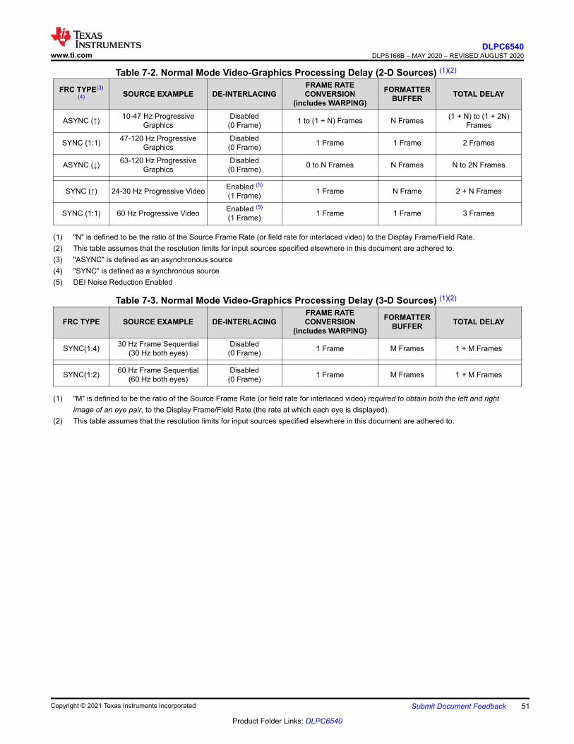
Table 7-2. Normal Mode Video-Graphics Processing Delay (2-D Sources) (1)(2) FRC TYPE(3)
(4) SOURCE EXAMPLE DE-INTERLACINGFRAME RATECONVERSION
(includes WARPING)
FORMATTERBUFFER TOTAL DELAY
ASYNC (↑) 10-47 Hz ProgressiveGraphics
Disabled(0 Frame) 1 to (1 + N) Frames N Frames (1 + N) to (1 + 2N)
Frames
SYNC (1:1) 47-120 Hz ProgressiveGraphics
Disabled(0 Frame) 1 Frame 1 Frame 2 Frames
ASYNC (↓) 63-120 Hz ProgressiveGraphics
Disabled(0 Frame) 0 to N Frames N Frames N to 2N Frames
SYNC (↑) 24-30 Hz Progressive Video Enabled (5)
(1 Frame) 1 Frame N Frame 2 + N Frames
SYNC (1:1) 60 Hz Progressive Video Enabled (5)
(1 Frame) 1 Frame 1 Frame 3 Frames
(1) "N" is defined to be the ratio of the Source Frame Rate (or field rate for interlaced video) to the Display Frame/Field Rate.(2) This table assumes that the resolution limits for input sources specified elsewhere in this document are adhered to.(3) "ASYNC" is defined as an asynchronous source(4) "SYNC" is defined as a synchronous source(5) DEI Noise Reduction Enabled
Table 7-3. Normal Mode Video-Graphics Processing Delay (3-D Sources) (1)(2)
FRC TYPE SOURCE EXAMPLE DE-INTERLACINGFRAME RATECONVERSION
(includes WARPING)
FORMATTERBUFFER TOTAL DELAY
SYNC(1:4) 30 Hz Frame Sequential(30 Hz both eyes)
Disabled(0 Frame) 1 Frame M Frames 1 + M Frames
SYNC(1:2) 60 Hz Frame Sequential(60 Hz both eyes)
Disabled(0 Frame) 1 Frame M Frames 1 + M Frames
(1) "M" is defined to be the ratio of the Source Frame Rate (or field rate for interlaced video) required to obtain both the left and rightimage of an eye pair, to the Display Frame/Field Rate (the rate at which each eye is displayed).
(2) This table assumes that the resolution limits for input sources specified elsewhere in this document are adhered to.
www.ti.comDLPC6540
DLPS168B – MAY 2020 – REVISED AUGUST 2020
Copyright © 2021 Texas Instruments Incorporated Submit Document Feedback 51
Product Folder Links: DLPC6540

7.3.3 V-by-One interface
The DLPC6540 Controller supports a single 8 lane V-by-One port which can be configured for 1, 2, 4 or 8lane use. This interface supports limited lane remapping which is shown inTable 7-4 . Intra-lane remapping (i.e.swapping P with N) is not supported.
Table 7-4. V-by-One Interface Lane Remapping OptionsV-by-One Port Physical Lanes (1)
Configuration (1) # of Lanes Lane 7 Lane 6 Lane 5 Lane 4 Lane 3 Lane 2 Lane 1 Lane 01 8 7 6 5 4 3 2 1 0
2 8 1 0 2 3 4 5 6 7
(1) There are two controller lane mapping options, with the option to use fewer than the full eight lanes for each of these.
Independent from the remapping of the physical V-by-One interface, the DLPC6540 supports a number of datamappings onto the actual physical interface as specified by the standard. V-by-One sources must match at leastone of these mappings These are shown in Table 7-5, Table 7-6, Table 7-7, Table 7-8, Table 7-9, Table 7-10,Table 7-11, Table 7-12, Table 7-13, and Table 7-14.
DLPC6540DLPS168B – MAY 2020 – REVISED AUGUST 2020 www.ti.com
52 Submit Document Feedback Copyright © 2021 Texas Instruments Incorporated
Product Folder Links: DLPC6540

Table 7-5. V-by-One Data Mapping for 36bpp/30bpp RGB/YCbCr 4:4:4V-by-One Data Map Mode 0V-by-One Input Data Bit 36bpp RGB/YCbCr 4:4:4 (1) 30bpp RGB/YCbCr 4:4:4 Mapper Output
D[0] R/Cr[4] R/Cr[2] B(2)
D[1] R/Cr[5] R/Cr[3] B(3)
D[2] R/Cr[6] R/Cr[4] B(4)
D[3] R/Cr[7] R/Cr(5] B(5)
D[4] R/Cr[8] R/Cr[6] B(6)
D[5] R/Cr[9] R/Cr[7] B(7)
D[6] R/Cr[10] R/Cr[8] B(8)
D[7] R/Cr[11] R/Cr[9] B(9)
D[8] G/Y[4] G/Y[2] A(2)
D[9] G/Y[5] G/Y[3] A(3)
D[10] G/Y[6] G/Y[4] A(4)
D[11] G/Y[7] G/Y[5] A(5)
D[12] G/Y[8] G/Y[6] A(6)
D[13] G/Y[9] G/Y[7] A(7)
D[14] G/Y[10] G/Y[8] A(8)
D[15] G/Y[11] G/Y[9] A(9)
D[16] B/Cb[4] B/Cb[2] C(2)
D[17] B/Cb[5] B/Cb[3] C(3)
D[18] B/Cb[6] B/Cb[4] C(4)
D[19] B/Cb[7] B/Cb[5] C(5)
D[20] B/Cb[8] B/Cb[6] C(6)
D[21] B/Cb[9] B/Cb[7] C(7)
D[22] B/Cb[10] B/Cb[8] C(8)
D[23] B/Cb[11] B/Cb[9] C(9)
D[24] - - -
D[25] - - -
D[26] B/Cb[2] B/Cb[1] C[0]
D[27] B/Cb[3] B/Cb[0] C[1]
D[28] G/Y[2] G/Y[1] A[0]
D[29] G/Y[3] G/Y[0] A[1]
D[30] R/Cr[2] R/Cr[1] B[0]
D[31] R/Cr[3] R/Cr[0] B[1]
(1) For 36-bit inputs, the 12-bits per color truncates to 10-bits per color with the two least significant-bits per color being discarded.
www.ti.comDLPC6540
DLPS168B – MAY 2020 – REVISED AUGUST 2020
Copyright © 2021 Texas Instruments Incorporated Submit Document Feedback 53
Product Folder Links: DLPC6540
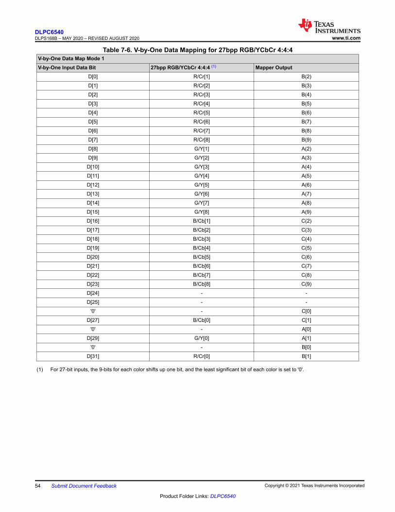
Table 7-6. V-by-One Data Mapping for 27bpp RGB/YCbCr 4:4:4V-by-One Data Map Mode 1V-by-One Input Data Bit 27bpp RGB/YCbCr 4:4:4 (1) Mapper Output
D[0] R/Cr[1] B(2)
D[1] R/Cr[2] B(3)
D[2] R/Cr[3] B(4)
D[3] R/Cr[4] B(5)
D[4] R/Cr[5] B(6)
D[5] R/Cr[6] B(7)
D[6] R/Cr[7] B(8)
D[7] R/Cr[8] B(9)
D[8] G/Y[1] A(2)
D[9] G/Y[2] A(3)
D[10] G/Y[3] A(4)
D[11] G/Y[4] A(5)
D[12] G/Y[5] A(6)
D[13] G/Y[6] A(7)
D[14] G/Y[7] A(8)
D[15] G/Y[8] A(9)
D[16] B/Cb[1] C(2)
D[17] B/Cb[2] C(3)
D[18] B/Cb[3] C(4)
D[19] B/Cb[4] C(5)
D[20] B/Cb[5] C(6)
D[21] B/Cb[6] C(7)
D[22] B/Cb[7] C(8)
D[23] B/Cb[8] C(9)
D[24] - -
D[25] - -
'0' - C[0]
D[27] B/Cb[0] C[1]
'0' - A[0]
D[29] G/Y[0] A[1]
'0' - B[0]
D[31] R/Cr[0] B[1]
(1) For 27-bit inputs, the 9-bits for each color shifts up one bit, and the least significant bit of each color is set to '0'.
DLPC6540DLPS168B – MAY 2020 – REVISED AUGUST 2020 www.ti.com
54 Submit Document Feedback Copyright © 2021 Texas Instruments Incorporated
Product Folder Links: DLPC6540

Table 7-7. V-by-One Data Mapping for 24bpp RGB/YCbCr 4:4:4V-by-One Data Map Mode 2V-by-One Input Data Bit 24bpp RGB/YCbCr 4:4:4 (1) Mapper Output
D[0] R/Cr[0] B(2)
D[1] R/Cr[1] B(3)
D[2] R/Cr[2] B(4)
D[3] R/Cr[3] B(5)
D[4] R/Cr[4] B(6)
D[5] R/Cr[5] B(7)
D[6] R/Cr[6] B(8)
D[7] R/Cr[7] B(9)
D[8] G/Y[0] A(2)
D[9] G/Y[1] A(3)
D[10] G/Y[2] A(4)
D[11] G/Y[3] A(5)
D[12] G/Y[4] A(6)
D[13] G/Y[5] A(7)
D[14] G/Y[6] A(8)
D[15] G/Y[7] A(9)
D[16] B/Cb[0] C(2)
D[17] B/Cb[1] C(3)
D[18] B/Cb[2] C(4)
D[19] B/Cb[3] C(5)
D[20] B/Cb[4] C(6)
D[21] B/Cb[5] C(7)
D[22] B/Cb[6] C(8)
D[23] B/Cb[7] C(9)
D[24] - -
D[25] - -
'0' - C[0]
'0' - C[1]
'0' - A[0]
'0' - A[1]
'0' - B[0]
'0' - B[1]
(1) For 24-bit inputs, the 8-bits for each color shifts up two bits, and the two least significant bits of each color are set to '0'.
www.ti.comDLPC6540
DLPS168B – MAY 2020 – REVISED AUGUST 2020
Copyright © 2021 Texas Instruments Incorporated Submit Document Feedback 55
Product Folder Links: DLPC6540

Table 7-8. V-by-One Data Mapping for 32bpp/24bpp/20bpp YCbCr 4:2:2 (1) V-by-One Data Map Mode 3V-by-One Input Data Bit 32bpp YCbCr 4:2:2 (2) 24bpp YCbCr 4:2:2 (3) 20bpp YCbCr 4:2:2 Mapper Output
D[0] CbCr[8] CbCr[4] CbCr[2] B(2)
D[1] CbCr[9] CbCr[5] CbCr[3] B(3)
D[2] CbCr[10] CbCr[6] CbCr[4] B(4)
D[3] CbCr[11] CbCr[7] CbCr[5] B(5)
D[4] CbCr[12] CbCr[8] CbCr[6] B(6)
D[5] CbCr[13] CbCr[8] CbCr[7] B(7)
D[6] CbCr[14] CbCr[10] CbCr[8] B(8)
D[7] CbCr[15] CbCr[11] CbCr[9] B(9)
D[8] Y[8] Y[4] Y[2] A(2)
D[9] Y[9] Y[5] Y[3] A(3)
D[10] Y[10] Y[6] Y[4] A(4)
D[11] Y[11] Y[7] Y[5] A(5)
D[12] Y[12] Y[8] Y[6] A(6)
D[13] Y[13] Y[9] Y[7] A(7)
D[14] Y[14] Y[10] Y[8] A(8)
D[15] Y[15] Y[11] Y[9] A(9)
'0' - - - C(2)
'0' - - - C(3)
'0' - - - C(4)
'0' - - - C(5)
'0' - - - C(6)
'0' - - - C(7)
'0' - - - C(8)
'0' - - - C(9)
D[24] - - - -
D[25] - - - -
'0' - - - C[0]
'0' - - - C[1]
D[28] Y[6] Y[2] Y[2] A[0]
D[29] Y[7] Y[3] Y[3] A[1]
D[30] CbCr[6] CbCr[2] CbCr[2] B[0]
D[31] CbCr[7] CbCr[3] CbCr[3] B[1]
(1) For all YCbCr 4:2:2 formats, data channel C is forced to "0".(2) For 32-bit inputs, the 16-bits per color truncates to 10-bit per color, with the six least significant-bits per color discarded.(3) For 24-bit inputs, the 12-bits per color truncates to 10-bit per color, with the two least significant-bits per color discarded.
DLPC6540DLPS168B – MAY 2020 – REVISED AUGUST 2020 www.ti.com
56 Submit Document Feedback Copyright © 2021 Texas Instruments Incorporated
Product Folder Links: DLPC6540

Table 7-9. V-by-One Data Mapping for 18bpp YCbCr 4:2:2(1) V-by-One Data Map Mode 4V-by-One Input Data Bit 18bpp YCbCr 4:2:2 (2) Mapper Output
D[0] CbCr[1] B(2)
D[1] CbCr[2] B(3)
D[2] CbCr[3] B(4)
D[3] CbCr[4] B(5)
D[4] CbCr[5] B(6)
D[5] CbCr[6] B(7)
D[6] CbCr[7] B(8)
D[7] CbCr[8] B(9)
D[8] Y[1] A(2)
D[9] Y[2] A(3)
D[10] Y[3] A(4)
D[11] Y[4] A(5)
D[12] Y[5] A(6)
D[13] Y[6] A(7)
D[14] Y[7] A(8)
D[15] Y[8] A(9)
'0' - C(2)
'0' - C(3)
'0' - C(4)
'0' - C(5)
'0' - C(6)
'0' - C(7)
'0' - C(8)
'0' - C(9)
D[24] - -
D[25] - -
'0' - C[0]
'0' - C[1]
'0' - A[0]
D[29] Y[0] A[1]
'0' - B[0]
D[31] CbCr[0] B[1]
(1) For all YCbCr 4:2:2 formats, data channel C is forced to "0".(2) For 18-bit inputs, the 9-bits for each color shifts up one bit, and the least significant bits of each color is set to '0'.
www.ti.comDLPC6540
DLPS168B – MAY 2020 – REVISED AUGUST 2020
Copyright © 2021 Texas Instruments Incorporated Submit Document Feedback 57
Product Folder Links: DLPC6540

Table 7-10. V-by-One Data Mapping for 16bpp YCbCr 4:2:2(1) V-by-One Data Map Mode 5V-by-One Input Data Bit 16bpp YCbCr 4:2:2 (2) Mapper Output
D[0] CbCr[0] B(2)
D[1] CbCr[1] B(3)
D[2] CbCr[2] B(4)
D[3] CbCr[3] B(5)
D[4] CbCr[4] B(6)
D[5] CbCr[5] B(7)
D[6] CbCr[6] B(8)
D[7] CbCr[7] B(9)
D[8] Y[0] A(2)
D[9] Y[1] A(3)
D[10] Y[2] A(4)
D[11] Y[3] A(5)
D[12] Y[4] A(6)
D[13] Y[5] A(7)
D[14] Y[6] A(8)
D[15] Y[7] A(9)
'0' - C(2)
'0' - C(3)
'0' - C(4)
'0' - C(5)
'0' - C(6)
'0' - C(7)
'0' - C(8)
'0' - C(9)
D[24] - -
D[25] - -
'0' - C[0]
'0' - C[1]
'0' - A[0]
'0' - A[1]
'0' - B[0]
'0' - B[1]
(1) For all YCbCr 4:2:2 formats, data channel C is forced to "0".(2) For 16-bit inputs, the 8-bits for each color shifts up one bit, and the least significant bit of each color is set to '0'.
DLPC6540DLPS168B – MAY 2020 – REVISED AUGUST 2020 www.ti.com
58 Submit Document Feedback Copyright © 2021 Texas Instruments Incorporated
Product Folder Links: DLPC6540

Table 7-11. V-by-One Data Mapping Example for 12bpp/10bpp YCbCr 4:2:0(1) V-by-One Data Map Mode 6V-by-One Input DataBit
12bpp YCbCr 4:2:0Even Line(2)
12bpp YCbCr 4:2:0Odd Line (2)
10bpp YCbCr 4:2:0Even Line
10bpp YCbCr 4:2:0Odd Line
Mapper Output
D[0] Y01[4] Y01[4] Y01[2] Y11[2] C(2)
D[1] Y01[5] Y01[5] Y01[3] Y11[3] C(3)
D[2] Y01[6] Y01[6] Y01[4] Y11[4] C(4)
D[3] Y01[7] Y01[7] Y01[5] Y11[5] C(5)
D[4] Y01[8] Y01[8] Y01[6] Y11[6] C(6)
D[5] Y01[9] Y01[9] Y01[7] Y11[7] C(7)
D[6] Y01[10] Y01[10] Y01[8] Y11[8] C(8)
D[7] Y01[11] Y01[11] Y01[9] Y11[9] C(9)
D[8] Y00[4] Y00[4] Y00[2] Y10[2] A(2)
D[9] Y00[5] Y00[5] Y00[3] Y10[3] A(3)
D[10] Y00[6] Y00[6] Y00[4] Y10[4] A(4)
D[11] Y00[7] Y00[7] Y00[5] Y10[5] A(5)
D[12] Y00[8] Y00[8] Y00[6] Y10[6] A(6)
D[13] Y00[9] Y00[9] Y00[7] Y10[7] A(7)
D[14] Y00[10] Y00[10] Y00[8] Y10[8] A(8)
D[15] Y00[11] Y00[11] Y00[9] Y10[9] A(9)
D[16] Cb00[4] Cr00[4] Cb00[2] Cr00[2] B(2)
D[17] Cb00[5] Cr00[5] Cb00[3] Cr00[3] B(3)
D[18] Cb00[6] Cr00[6] Cb00[4] Cr00[4] B(4)
D[19] Cb00[7] Cr00[7] Cb00[5] Cr00[5] B(5)
D[20] Cb00[8] Cr00[8] Cb00[6] Cr00[6] B(6)
D[21] Cb00[9] Cr00[9] Cb00[7] Cr00[7] B(7)
D[22] Cb00[10] Cr00[10] Cb00[8] Cr00[8] B(8)
D[23] Cb00[11] Cr00[11] Cb00[9] Cr00[9] B(9)
D[24] - - - - -
D[25] - - - - -
D[26] Cb00[2] Cr00[2] Cb00[0] Cr00[0] B[0]
D[27] Cb00[3] Cr00[3] Cb00[1] Cr00[1] B[1]
D[28] Y00[2] Y10[2] Y00[0] Y10[0] A[0]
D[29] Y00[3] Y10[3] Y00[1] Y10[1] A[1]
D[30] Y01[2] Y11[2] Y01[0] Y11[0] C[0]
D[31] Y01[3] Y11[3] Y01[1] Y11[1] C[1]
(1) For all YCbCr 4:2:0 inputs, two consecutive pixel Luma values are brought in on each clock. Even lines carry the Cb values, and oddlines carry the Cr values.
(2) For 12bpp YCbCr 4:2:0 inputs, the 12-bits per color truncates to 10-bits per color with the two least significant-bits per color discarded.
www.ti.comDLPC6540
DLPS168B – MAY 2020 – REVISED AUGUST 2020
Copyright © 2021 Texas Instruments Incorporated Submit Document Feedback 59
Product Folder Links: DLPC6540

Table 7-12. V-by-One Data Mapping Example for 8bpp YCbCr 4:2:0(1) V-by-One Data Map Mode 7V-by-One Input Data Bit 8bpp YCbCr 4:2:0
Even Line (2)8bpp YCbCr 4:2:0Odd Line (2)
Mapper Output
D[0] Y01[0] Y11[0] C(2)
D[1] Y01[1] Y11[1] C(3)
D[2] Y01[2] Y11[2] C(4)
D[3] Y01[3] Y11[3] C(5)
D[4] Y01[4] Y11[4] C(6)
D[5] Y01[5] Y11[5] C(7)
D[6] Y01[6] Y11[6] C(8)
D[7] Y01[7] Y11[7] C(9)
D[8] Y00[0] Y10[0] A(2)
D[9] Y00[1] Y10[1] A(3)
D[10] Y00[2] Y10[2] A(4)
D[11] Y00[3] Y10[3] A(5)
D[12] Y00[4] Y10[4] A(6)
D[13] Y00[5] Y10[5] A(7)
D[14] Y00[6] Y10[6] A(8)
D[15] Y00[7] Y10[7] A(9)
D[16] Cb00[0] Cr00[0] B(2)
D[17] Cb00[1] Cr00[1] B(3)
D[18] Cb00[2] Cr00[2] B(4)
D[19] Cb00[3] Cr00[3] B(5)
D[20] Cb00[4] Cr00[4] B(6)
D[21] Cb00[5] Cr00[5] B(7)
D[22] Cb00[6] Cr00[6] B(8)
D[23] Cb00[7] Cr00[7] B(9)
D[24] - - -
D[25] - - -
'0' - - B[0]
'0' - - B[1]
'0' - - A[0]
'0' - - A[1]
'0' - - C[0]
'0' - - C[1]
(1) For all YCbCr 4:2:0 inputs, two consecutive pixel Luma values are brought in on each clock. Even lines carry the Cb values, and oddlines carry the Cr values.
(2) For 8bpp YCbCr 4:2:0 inputs, the 8-bits for each color shifts up two bits, and the two least significant bits of each color are set to '0'.
DLPC6540DLPS168B – MAY 2020 – REVISED AUGUST 2020 www.ti.com
60 Submit Document Feedback Copyright © 2021 Texas Instruments Incorporated
Product Folder Links: DLPC6540

Table 7-13. V-by-One Data Mapping Example for 10bpp YCbCr 4:2:0 (1) V-by-One Data Map Mode 8V-by-One Input Data Bit 10bpp YCbCr 4:2:0
Even Line10bpp YCbCr 4:2:0Odd Line
Mapper Output
D[0] Y00[2] Y10[2] A(2)
D[1] Y003] Y10[3] A(3)
D[2] Y00[4] Y10[4] A(4)
D[3] Y00[5] Y10[5] A(5)
D[4] Y00[6] Y10[6] A(6)
D[5] Y00[7] Y10[7] A(7)
D[6] Y00[8] Y10[8] A(8)
D[7] Y00[9] Y10[9] A(9)
D[8] Cb00[2] Cr00[2] B(2)
D[9] Cb00[3] Cr00[3] B(3)
D[10] Cb00[4] Cr00[4] B(4)
D[11] Cb00[5] Cr00[5] B(5)
D[12] Cb00[6] Cr00[6] B(6)
D[13] Cb00[7] Cr00[7] B(7)
D[14] Cb00[8] Cr00[8] B(8)
D[15] Cb00[9] Cr00[9] B(9)
D[16] Y01[2] Y11[2] C(2)
D[17] Y01[3] Y11[3] C(3)
D[18] Y01[4] Y11[4] C(4)
D[19] Y01[5] Y11[5] C(5)
D[20] Y01[6] Y11[6] C(6)
D[21] Y01[7] Y11[7] C(7)
D[22] Y01[8] Y11[8] C(8)
D[23] Y01[9] Y11[9] C(9)
D[24] - - -
D[25] - - -
D[26] Y01[0] Y11[0] C[0]
D[27] Y01[1] Y11[1] C[1]
D[28] Cb00[0] Cr00[0] B[0]
D[29] Cb00[1] Cr00[1] B[1]
D[30] Y00[0] Y10[0] A[0]
D[31] Y00[1] Y10[1] A[1]
(1) For all YCbCr 4:2:0 inputs, two consecutive pixel Luma values are brought in on each clock. Even lines carry Cb values, and odd linescarry the Cr values.
www.ti.comDLPC6540
DLPS168B – MAY 2020 – REVISED AUGUST 2020
Copyright © 2021 Texas Instruments Incorporated Submit Document Feedback 61
Product Folder Links: DLPC6540
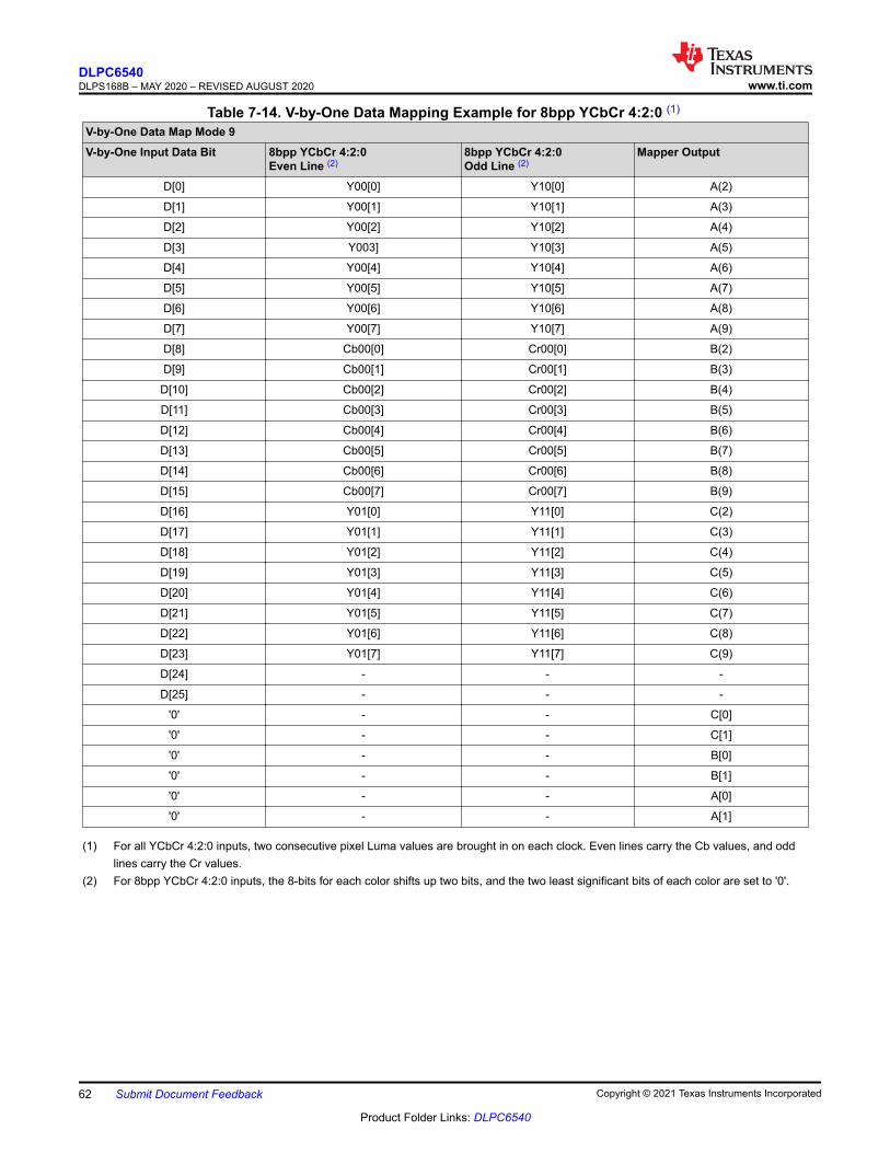
Table 7-14. V-by-One Data Mapping Example for 8bpp YCbCr 4:2:0 (1) V-by-One Data Map Mode 9V-by-One Input Data Bit 8bpp YCbCr 4:2:0
Even Line (2)8bpp YCbCr 4:2:0Odd Line (2)
Mapper Output
D[0] Y00[0] Y10[0] A(2)
D[1] Y00[1] Y10[1] A(3)
D[2] Y00[2] Y10[2] A(4)
D[3] Y003] Y10[3] A(5)
D[4] Y00[4] Y10[4] A(6)
D[5] Y00[5] Y10[5] A(7)
D[6] Y00[6] Y10[6] A(8)
D[7] Y00[7] Y10[7] A(9)
D[8] Cb00[0] Cr00[0] B(2)
D[9] Cb00[1] Cr00[1] B(3)
D[10] Cb00[2] Cr00[2] B(4)
D[11] Cb00[3] Cr00[3] B(5)
D[12] Cb00[4] Cr00[4] B(6)
D[13] Cb00[5] Cr00[5] B(7)
D[14] Cb00[6] Cr00[6] B(8)
D[15] Cb00[7] Cr00[7] B(9)
D[16] Y01[0] Y11[0] C(2)
D[17] Y01[1] Y11[1] C(3)
D[18] Y01[2] Y11[2] C(4)
D[19] Y01[3] Y11[3] C(5)
D[20] Y01[4] Y11[4] C(6)
D[21] Y01[5] Y11[5] C(7)
D[22] Y01[6] Y11[6] C(8)
D[23] Y01[7] Y11[7] C(9)
D[24] - - -
D[25] - - -
'0' - - C[0]
'0' - - C[1]
'0' - - B[0]
'0' - - B[1]
'0' - - A[0]
'0' - - A[1]
(1) For all YCbCr 4:2:0 inputs, two consecutive pixel Luma values are brought in on each clock. Even lines carry the Cb values, and oddlines carry the Cr values.
(2) For 8bpp YCbCr 4:2:0 inputs, the 8-bits for each color shifts up two bits, and the two least significant bits of each color are set to '0'.
DLPC6540DLPS168B – MAY 2020 – REVISED AUGUST 2020 www.ti.com
62 Submit Document Feedback Copyright © 2021 Texas Instruments Incorporated
Product Folder Links: DLPC6540

7.3.4 DMD (HSSI) Interface
The DLPC6540 Controller DMD interface supports two High Speed Serial Interface (HSSI) output-only interfacesfor data transmission, a single low speed LVDS output-only interface for command write transactions, as wellas a low speed single-ended input interface used for command read transactions. Each HSSI port supports fulldata-only inter-lane remapping within the port, but not between ports. When utilizing this feature, each uniquedata lane pair can only be mapped to one unique destination data lane pair, and Intra-lane remapping (i.e.swapping P with N) is not supported. In addition, the two HSSI ports can also be swapped. Lane and portremapping (specified in flash) can help with board layout as needed. The number of HSSI ports and number ofHSSI lanes/per HSSI port required are based on DMD type and DMD display resolution. Table 7-15 shows someremapping examples. When both ports are used, they do not need to have the same pin mapping.
Table 7-15. Controller to DMD Pin Mapping ExamplesDLPC6540 Controller PINS - REMAPPING EXAMPLES TO DMD PINS
DMD PINSBASELINE FLIP HSSI0 180
No FLIP HSSI1SWAP HSSI0 PORTWITH HSSI1 PORT
SWAP HSSI0 PORTWITH HSSI1 PORT ANDMIXED REMAPPING
DMD_HSSI0_D0_PDMD_HSSI0_D0_N
DMD_HSSI0_D7_PDMD_HSSI0_D7_N
DMD_HSSI1_D0_PDMD_HSSI1_D0_N
DMD_HSSI1_D2_PDMD_HSSI1_D2_N
DMD_HSSI0_D0_PDMD_HSSI0_D0_N
DMD_HSSI0_D1_PDMD_HSSI0_D1_N
DMD_HSSI0_D6_PDMD_HSSI0_D6_N
DMD_HSSI1_D1_PDMD_HSSI1_D1_N
DMD_HSSI1_D3_PDMD_HSSI1_D3_N
DMD_HSSI0_D1_PDMD_HSSI0_D1_N
DMD_HSSI0_D2_PDMD_HSSI0_D2_N
DMD_HSSI0_D5_PDMD_HSSI0_D5_N
DMD_HSSI1_D2_PDMD_HSSI1_D2_N
DMD_HSSI1_D0_PDMD_HSSI1_D0_N
DMD_HSSI0_D2_PDMD_HSSI0_D2_N
DMD_HSSI0_D3_PDMD_HSSI0_D3_N
DMD_HSSI0_D4_PDMD_HSSI0_D4_N
DMD_HSSI1_D3_PDMD_HSSI1_D3_N
DMD_HSSI1_D1_PDMD_HSSI1_D1_N
DMD_HSSI0_D3_PDMD_HSSI0_D3_N
DMD_HSSI0_D4_PDMD_HSSI0_D4_N
DMD_HSSI0_D3_PDMD_HSSI0_D3_N
DMD_HSSI1_D4_PDMD_HSSI1_D4_N
DMD_HSSI1_D6_PDMD_HSSI1_D6_N
DMD_HSSI0_D4_PDMD_HSSI0_D4_N
DMD_HSSI0_D5_PDMD_HSSI0_D5_N
DMD_HSSI0_D2_PDMD_HSSI0_D2_N
DMD_HSSI1_D5_PDMD_HSSI1_D5_N
DMD_HSSI1_D7_PDMD_HSSI1_D7_N
DMD_HSSI0_D5_PDMD_HSSI0_D5_N
DMD_HSSI0_D6_PDMD_HSSI0_D6_N
DMD_HSSI0_D1_PDMD_HSSI0_D1_N
DMD_HSSI1_D6_PDMD_HSSI1_D6_N
DMD_HSSI1_D4_PDMD_HSSI1_D4_N
DMD_HSSI0_D6_PDMD_HSSI0_D6_N
DMD_HSSI0_D7_PDMD_HSSI0_D7_N
DMD_HSSI0_D0_PDMD_HSSI0_D0_N
DMD_HSSI1_D7_PDMD_HSSI1_D7_N
DMD_HSSI1_D5_PDMD_HSSI1_D5_N
DMD_HSSI0_D7_PDMD_HSSI0_D7_N
DMD_HSSI1_D0_PDMD_HSSI1_D0_N
DMD_HSSI1_D0_PDMD_HSSI1_D0_N
DMD_HSSI0_D0_PDMD_HSSI0_D0_N
DMD_HSSI0_D6_PDMD_HSSI0_D6_N
DMD_HSSI1_D0_PDMD_HSSI1_D0_N
DMD_HSSI1_D1_PDMD_HSSI1_D1_N
DMD_HSSI1_D1_PDMD_HSSI1_D1_N
DMD_HSSI0_D1_PDMD_HSSI0_D1_N
DMD_HSSI0_D7_PDMD_HSSI0_D7_N
DMD_HSSI1_D1_PDMD_HSSI1_D1_N
DMD_HSSI1_D2_PDMD_HSSI1_D2_N
DMD_HSSI1_D2_PDMD_HSSI1_D2_N
DMD_HSSI0_D2_PDMD_HSSI0_D2_N
DMD_HSSI0_D4_PDMD_HSSI0_D4_N
DMD_HSSI1_D2_PDMD_HSSI1_D2_N
DMD_HSSI1_D3_PDMD_HSSI1_D3_N
DMD_HSSI1_D3_PDMD_HSSI1_D3_N
DMD_HSSI0_D3_PDMD_HSSI0_D3_N
DMD_HSSI0_D5_PDMD_HSSI0_D5_N
DMD_HSSI1_D3_PDMD_HSSI1_D3_N
DMD_HSSI1_D4_PDMD_HSSI1_D4_N
DMD_HSSI1_D4_PDMD_HSSI1_D4_N
DMD_HSSI0_D4_PDMD_HSSI0_D4_N
DMD_HSSI0_D2_PDMD_HSSI0_D2_N
DMD_HSSI1_D4_PDMD_HSSI1_D4_N
DMD_HSSI1_D5_PDMD_HSSI1_D5_N
DMD_HSSI1_D5_PDMD_HSSI1_D5_N
DMD_HSSI0_D5_PDMD_HSSI0_D5_N
DMD_HSSI0_D3_PDMD_HSSI0_D3_N
DMD_HSSI1_D5_PDMD_HSSI1_D5_N
DMD_HSSI1_D6_PDMD_HSSI1_D6_N
DMD_HSSI1_D6_PDMD_HSSI1_D6_N
DMD_HSSI0_D6_PDMD_HSSI0_D6_N
DMD_HSSI0_D0_PDMD_HSSI0_D0_N
DMD_HSSI1_D6_PDMD_HSSI1_D6_N
DMD_HSSI1_D7_PDMD_HSSI1_D7_N
DMD_HSSI1_D7_PDMD_HSSI1_D7_N
DMD_HSSI0_D7_PDMD_HSSI0_D7_N
DMD_HSSI0_D1_PDMD_HSSI0_D1_N
DMD_HSSI1_D7_PDMD_HSSI1_D7_N
www.ti.comDLPC6540
DLPS168B – MAY 2020 – REVISED AUGUST 2020
Copyright © 2021 Texas Instruments Incorporated Submit Document Feedback 63
Product Folder Links: DLPC6540

7.3.5 Program Memory Flash Interface
The DLPC6540 provides three external program memory chip selects for devices to access the programmemory interface. These are detailed in Table 7-16.
Table 7-16. Program Memory Interface Chip SelectsCHIP SELECT
NAME CHIP SELECT USE DATA BUS WIDTH ACCESS TIME MAXIMUM SIZESUPPORTED (1)
PM_CSZ_0 Boot FLASH only - Required (2) 16 bits < = 120ns 256Mb
PM_CSZ_1 Additional Peripheral Device (or additionalFLASH) - Optional
16 bits < = 120ns 256Mb
PM_CSZ_2 Additional Peripheral Device - Optional 16 bits < = 120ns 256Mb
(1) Using GPIO_47 as additional address bit(2) Boot FLASH type supported is Standard NOR parallel FLASH, single or multi-bank.
FLASH access timing is software programmable with up to 31 wait states. Additional information about read andwrite wait state timing is provided in Table 7-17 and Figure 7-2.
Table 7-17. Program Memory Wait State TimingPARAMETER EQUATION (1)
TWSR: Wait State Resolution 6ns
Read Wait States(Number of Read Wait States for each CSz read access)
ROUNDUP(MAX(TACC, TCE,TOE)/TWSR-N) (2) (3)
Write Wait States for TCSand TAS(Time from CS/Address activation to WRZ assertion)
ROUNDUP(MAX(TCS+5ns, TAS+5ns)/TWSR-N) (2)
Write Wait States for TWP and TDS(Time from WRZ assertion to WEZ de-assertion)
ROUNDUP(MAX(TWP+5ns, TDS+5ns)/TWSR-N) (2)
Write Wait States for TCHand TDH(Time from CS/Address activation to WRZ assertion)
ROUNDUP(MAX(TCH+5ns, TDH+5ns)/TWSR-N) (2)
(1) a. TACC: Read Access Time (ADDR to DATA valid) – (address valid to DATA valid)b. TCE: Read Access Time (CSZ to DATA valid) – (chip select active to DATA valid)c. TOE: Read Access Time (OEZ to DATA valid) – (output enable active to DATA valid)d. TCS: CSZ Setup Time (Writes) – (chip select active before negedge(WEZ)e. TCS: Address Setup Time (Writes) – (address valid before negedge(WEZ)f. TAS: Address Setup Time (Writes) – (address valid before negedge(WEZ)g. TWP: Write Pulse Width (Writes) – (WEZ active low time)h. TDS: Data Setup Time (Writes) – (DATA valid before posedge(WEZ)i. TCH: CSZ Hold Time (Writes) – (CSZ held active after posedge(WEZ)j. TDH: Data Hold Time (Writes) – (DATA held valid after posedge(WEZ)
(2) Requires a minimum of at least 1 wait state(3) Assumes a maximum single direction trace length of 90 mm (3.5 inches)
DLPC6540DLPS168B – MAY 2020 – REVISED AUGUST 2020 www.ti.com
64 Submit Document Feedback Copyright © 2021 Texas Instruments Incorporated
Product Folder Links: DLPC6540
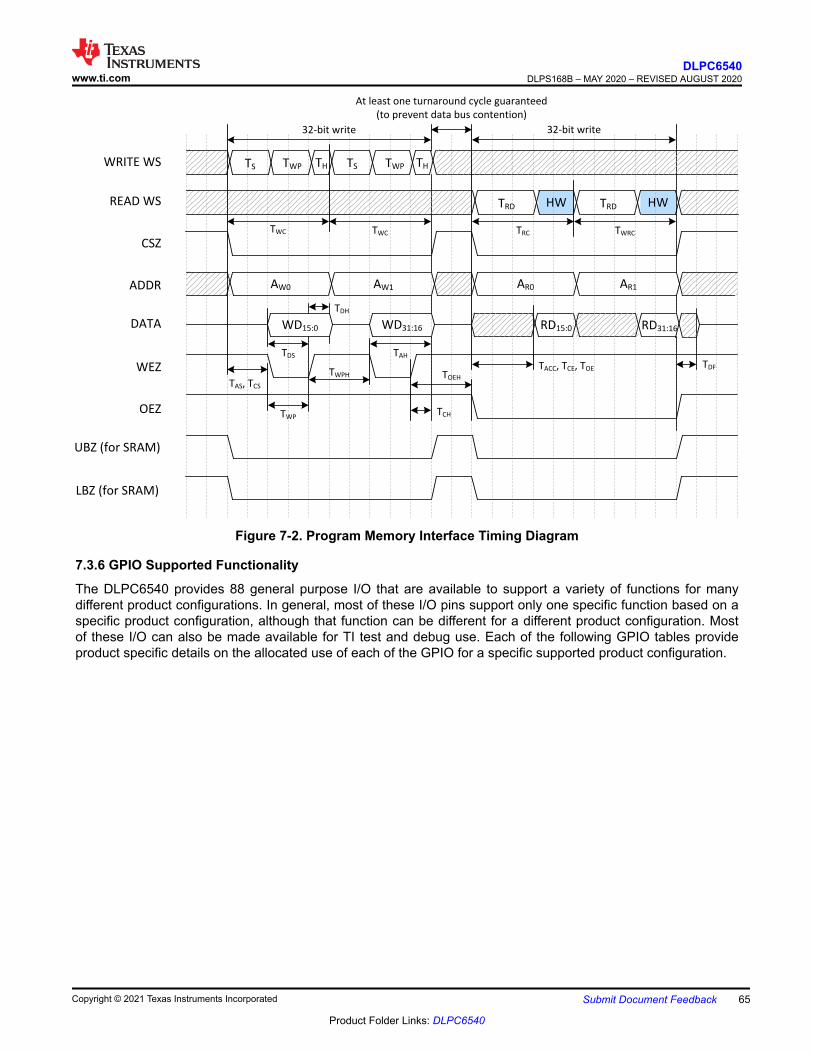
TSWRITE WS
CSZ
LBZ (for SRAM)
TWP TH TWP THTS
TRD HW TRD HWREAD WS
ADDR AW0 AW1 AR0 AR1
WD15:0 WD31:16 RD15:0 RD31:16DATA
WEZ
OEZ
UBZ (for SRAM)
TWC TWC
32-bit write 32-bit write
TRC TWRC
At least one turnaround cycle guaranteed
(to prevent data bus contention)
TDFTACC, TCE, TOETOEH
TCHTWP
TWPH
TDS
TDH
TAH
TAS, TCS
Figure 7-2. Program Memory Interface Timing Diagram
7.3.6 GPIO Supported Functionality
The DLPC6540 provides 88 general purpose I/O that are available to support a variety of functions for manydifferent product configurations. In general, most of these I/O pins support only one specific function based on aspecific product configuration, although that function can be different for a different product configuration. Mostof these I/O can also be made available for TI test and debug use. Each of the following GPIO tables provideproduct specific details on the allocated use of each of the GPIO for a specific supported product configuration.
www.ti.comDLPC6540
DLPS168B – MAY 2020 – REVISED AUGUST 2020
Copyright © 2021 Texas Instruments Incorporated Submit Document Feedback 65
Product Folder Links: DLPC6540

Table 7-18. GPIO Supported Functionality - LED with DLPA3005 (1) GPIO SIGNAL NAME DESCRIPTION
GPIO_00 SSP1_SCLK (I) SSP Master or Slave
GPIO_01 SSP1_DI (I) SSP Master or Slave
GPIO_02 SSP1_DO (O) SSP Master or Slave
GPIO_03 SSP1_CSZ0 (I) SSP Master or Slave
GPIO_04 SSP1_CSZ1 (I) SSP Master or Slave
GPIO_05 SSP1_CSZ2 (I) SSP Master or Slave
GPIO_06 SAS_CLK (O)
GPIO_07 SAS_DI (I)
GPIO_08 SAS_DO (O)
GPIO_09 SAS_CSZ (O)
GPIO_10 SAS_INTGTR_EN (O)
GPIO_11 IIC1_SCL (B)
GPIO_12 IIC1_SDA (B)
GPIO_13 UART1_TXD (O)
GPIO_14 UART1_RXD (I)
GPIO_15 UART1_CTSZ (I)
GPIO_16 UART1_RTSZ (O)
GPIO_17 General Purpose Input/Output Available for general host use via Host Commands
GPIO_18 IR0 (I)
GPIO_19 IR1 (I)
GPIO_20 PWM-IN0 (I)
GPIO_21 PWM-IN1 (I)
GPIO_22 3D LR (I) For 3D applications: Left or right 3D reference (left = 1, right = 0). Tobe provided by the host when a 3D command is not provided. Musttransition in the middle of each frame (no closer than 1 ms to the activeedge of VSYNC)
GPIO_23 LL_FAULT (O)
GPIO_24 LEDSEL_0 (O)
GPIO_25 LEDSEL_1 (O)
GPIO_26 General Purpose Input/Output Available for general host use via Host Commands
GPIO_27 General Purpose Input/Output Available for general host use via Host Commands
GPIO_28 Heartbeat (O)
GPIO_29 General Purpose Input/Output Available for general host use via Host Commands
GPIO_30 VBIAS_MON (I)
GPIO_31 HDMI_CEC (B)
GPIO_32 IIC2_SCL (B)
GPIO_33 IIC2_SDA (B)
GPIO_34 WRP_TRIG_OUT (O)
GPIO_35 DAO_DO_0 (O)
DLPC6540DLPS168B – MAY 2020 – REVISED AUGUST 2020 www.ti.com
66 Submit Document Feedback Copyright © 2021 Texas Instruments Incorporated
Product Folder Links: DLPC6540

Table 7-18. GPIO Supported Functionality - LED with DLPA3005 (1) (continued)GPIO SIGNAL NAME DESCRIPTION
GPIO_36 DAO_DO_1 (O)
GPIO_37 DAO_CLKOUT (O)
GPIO_38 HBT_DO (O)
GPIO_39 HBT_CLKOUT (O)
GPIO_40 SSP2_SCLK (I) SSP Master
GPIO_41 SSP2_DI (I) SSP Master
GPIO_42 SSP2_DO (O) SSP Master
GPIO_43 SSP2_CSZ0 (I) SSP Master
GPIO_44 SSP2_CSZ1 (I) SSP Master
GPIO_45 SSP2_CSZ2 (I) SSP Master
GPIO_46 General Purpose Input/Output Available for general host use via Host Commands
GPIO_47 PM_ADDR_23 (O)
GPIO_48 USB OTG Charge Pump Enable (O)
GPIO_49 SSP0_CSZ4 (O) DLPA3005
GPIO_50 SSP0_CSZ3 (O)
GPIO_51 General Purpose Input/Output Available for general host use via Host Commands
GPIO_52 LED_Enable (O)
GPIO_53 General Purpose Input/Output Available for general host use via Host Commands
GPIO_54 General Purpose Input/Output Available for general host use via Host Commands
GPIO_55 General Purpose Input/Output Available for general host use via Host Commands
GPIO_56 General Purpose Input/Output Available for general host use via Host Commands
GPIO_57 General Purpose Input/Output Available for general host use via Host Commands
GPIO_58 I2C_BUSY (O)
GPIO_59 General Purpose Input/Output Available for general host use via Host Commands
GPIO_60 General Purpose Input/Output Available for general host use via Host Commands
GPIO_61 General Purpose Input/Output Available for general host use via Host Commands
GPIO_62 General Purpose Input/Output Available for general host use via Host Commands
GPIO_63 PROJ_ON (I)
GPIO_64 HOLD_BOOTZ (I)
GPIO_65 4 way XPR (O)
GPIO_66 4 way XPR (O)
GPIO_67 4 way XPR (O)
GPIO_68 4 way XPR (O)
GPIO_69 4 way XPR (O)
GPIO_70 4 way XPR (O)
GPIO_71 4 way XPR (O)
GPIO_72 4 way XPR (O)
GPIO_73 4 way XPR (O)
www.ti.comDLPC6540
DLPS168B – MAY 2020 – REVISED AUGUST 2020
Copyright © 2021 Texas Instruments Incorporated Submit Document Feedback 67
Product Folder Links: DLPC6540

Table 7-18. GPIO Supported Functionality - LED with DLPA3005 (1) (continued)GPIO SIGNAL NAME DESCRIPTION
GPIO_74 4 way XPR (O)
GPIO_75 4 way XPR (O)
GPIO_76 4 way XPR (O)
GPIO_77 General Purpose Input/Output Available for general host use via Host Commands
GPIO_78 General Purpose Input/Output Available for general host use via Host Commands
GPIO_79 General Purpose Input/Output Available for general host use via Host Commands
GPIO_80 General Purpose Input/Output Available for general host use via Host Commands
GPIO_81 General Purpose Input/Output Available for general host use via Host Commands
GPIO_82 General Purpose Input/Output Available for general host use via Host Commands
GPIO_83 General Purpose Input/Output Available for general host use via Host Commands
GPIO_84 General Purpose Input/Output Available for general host use via Host Commands
GPIO_85 General Purpose Input/Output Available for general host use via Host Commands
GPIO_86 General Purpose Input/Output Available for general host use via Host Commands
GPIO_87 General Purpose Input/Output Available for general host use via Host Commands
(1) All GPIO that are listed as General Purpose Input/Output must be configured as an input, a standard output, or an open-drain output.This is set in the flash configuration. It is suggested that all unused General Purpose Input/Output GPIO should be configured as alogic zero output and be left unconnected, otherwise an external pull-up or pull-down will be required to avoid a floating input. It shouldbe noted that the reset default for all GPIO is as an input signal. It should also be noted that an external pull-up (≤ 10kΩ) is required foreach signal configured as open-drain output.
7.3.7 Debug Support
The DLPC6540 contains a test point output port, TSTPT_(7:0), which provides the Host with the ability to providefor Controller debug support. For initial debug operation, the four signals (TSTPT(3:0)) are sampled as inputsapproximately 1.5 µs after PWRGOOD goes high (or after a system reset). Once their input state has beensampled and captured, this information is used to setup the initial test mode output state of the TSTPT_(7:0)bus. Table 7-19 defines the test mode selection for a few programmable output states for TSTPT_(7:0). Use thedefault state of 0000 (defined by the required external pulldown resistors) for normal operation (that is, no debugrequired).
To allow TI to make use of this debug capability, providing for the option of a jumper to an external pullup isrecommended for TSTPT(3:0), as well as providing access to allow observation of the TSTPT bus outputs.
Table 7-19. Examples of Test Mode Selection Outputs Defined by TSTPT(3:0)(1)
TSTPT_(7:0)OUTPUT
TSTPT(3:0) CAPTURED VALUES0000 (DEFAULT)(NO SWITCHINGACTIVITY)
0101CLOCK DEBUG
1000SYSTEM CALIBRATION
TSTPT(0) 0 HIGH Vertical Sync
TSTPT(1) 0 166.25 MHz Delayed CW Index
TSTPT(2) 0 83.13 MHz Sequence Index
TSTPT(3) 0 41.56 MHz CW Spoke Test Point
TSTPT(4) 0 10.39 MHz CW Revolution Test Point
TSTPT(5) 0 25.16 MHz Reset Sequence Aux Bit 0
TSTPT(6) 0 133.00 MHz Reset Sequence Aux Bit 1
TSTPT(7) 0 HIGH Reset Sequence Aux Bit 2
(1) These are only the default output selections. Software can reprogram the selection at any time.
DLPC6540DLPS168B – MAY 2020 – REVISED AUGUST 2020 www.ti.com
68 Submit Document Feedback Copyright © 2021 Texas Instruments Incorporated
Product Folder Links: DLPC6540

7.4 Device Operational ModesThe DLPC6540 has two operational modes which are enabled via software command via the Host controlinterface. These modes are Standby and Active.
7.4.1 Standby Mode
The system is powered up and active, however, most blocks within the Controller have been shut down toconserve power. Only the µProcessor and its peripherals are active (supporting a dormant projector waiting to bewoken up). In this mode the DMD is parked and no image can be displayed.
7.4.2 Active Mode
The system is powered up and fully operational, capable of projecting internal or external source images.
7.4.2.1 Normal Configuration
This configuration enables the full functionality of the DLPC6540.
www.ti.comDLPC6540
DLPS168B – MAY 2020 – REVISED AUGUST 2020
Copyright © 2021 Texas Instruments Incorporated Submit Document Feedback 69
Product Folder Links: DLPC6540

8 Application and ImplementationNote
Information in the following applications sections is not part of the TI component specification,and TI does not warrant its accuracy or completeness. TI’s customers are responsible fordetermining suitability of components for their purposes, as well as validating and testing their designimplementation to confirm system functionality.
8.1 Application InformationThe DLPC6540 display controller is part of the DLP471TP chipset. The controller integrates all system imageprocessing and control and DMD data formatting onto a single integrated circuit (IC). It supports LED illuminationsystems, and it also includes multiple image processing algorithms such as DynamicBlack. Applications ofinterest include 4K UHD display applications, Mobile smart TV, digital signage and commercial gaming.
8.2 Typical ApplicationThe DLPC6540 controller works for applications requiring high brightness and high resolution displays.DLPC6540 display controller is combined with the DLP471TP DMD, LED power management device DLPA3005and other electrical, optical and mechanical components, the chipset enables bright, affordable, full 4K UHDdisplay solutions. A typical 4K UHD system application using the DLPC6540 controllers and DLP471TP DMD isshown here
DLPC6540
Master
DLPA3005
TI DLP chipset
Third party component
VBIAS, VOFFSET, VRESET
SYSPWR (14.5 V to 20 V)
PWRGOOD
LS Interface
PROJ_ON
I2C
I2C BUSY
Vx1
2-Port HSSI
GPIO (PROJ_ON)
GPIO
SPI BUS (Ctrl) (4)
POSENSE
Front End
Device
Vx1:
3840 × 2160
@ 60Hz
USB Mux
DC
SupplyVSPI1.8 V
1.1
Reg
1.1 V @ 3 A
L3
LDO 2
LED_SEL (2)
1.8
Reg
USB Camera
Actuator
Driver
4-Position
Actuator
Flash (2)
(23) (18)ADDR DATA
3D L/R
Fan or
programmable DC supply
RESETZ
INITZ
DC
Reg
L4
L5
1.8 V @ 3 A for
DMD and DLPC6540
LDO 1 3.3 V @ 2 A2.5 V
DLPC471TP
.47 4K UHD DMD
VLED
L1
RLIM current sense
SYSPWR
L2
(3)
1.21 V1.8 V3.3 V
1.15 V
USB 2.01.8 V
I2C EEPROM
SPI (2)
Figure 8-1. Typical 4K UHD DLPA3005 Display Application
8.2.1 Design Requirements
The display controller is the digital interface between the DMD and the rest of the system. The display controllertakes digital V-by-One input from front end receiver and drives the DMD over a high speed interface. The displaycontroller also generates the necessary signals (data, protocols, timings) required to display images on theDMD. Reliable operation of the DMD is only insured when the DMD and the controller are used together in asystem. In addition to the DLP devices in the chipset, other devices may be needed. Typically, a Flash part isneeded to store the software and firmware and power supply management part required to power the DMD andthe controller.
DLPC6540DLPS168B – MAY 2020 – REVISED AUGUST 2020 www.ti.com
70 Submit Document Feedback Copyright © 2021 Texas Instruments Incorporated
Product Folder Links: DLPC6540

8.2.2 Detailed Design Procedure
For connecting the DLPC6540 controller and the DLP471TP DMD together, see the reference design schematic.Layout guidelines should be followed to achieve a reliable projector. To complete the DLP system, an opticalmodule or light engine is required that contains the DLP471TP DMD, associated illumination sources, opticalelements, and necessary mechanical components.
www.ti.comDLPC6540
DLPS168B – MAY 2020 – REVISED AUGUST 2020
Copyright © 2021 Texas Instruments Incorporated Submit Document Feedback 71
Product Folder Links: DLPC6540

9 Power Supply Recommendations9.1 Power Supply ManagementThe DLPA3005 manages power for the DLPC6540 and DMD. See Section 6.12 for all power sequencing andtiming requirements.
9.2 Hot Plug UsageWhile the V-by-One, FPD-Link, and USB interfaces support hot plug usage (i.e. these interfaces can beconnected and disconnected while the DLPC6540 is powered), the controller itself (and any DMD connectedto the system) do not support Hot Plug use. As such, power down the system prior to removing the controller orDMD from any system.
9.3 Power Supplies for Unused Input Source InterfacesWhile certain product configurations cannot offer or make use of all of the available input source interfaces (e.g.V-by-One, FPD-Link), the power supplies that are associated with these unused input source interfaces must stillbe provided as if the interface was actually being used. The only concession is that the ferrite based isolationfilters for these supplies can be simplified down to simple de-coupling caps.
9.4 Power Supplies9.4.1 1.15-V Power Supplies
The DLPC6540 can support a low cost power delivery system with a single 1.15-V power source derived froma switching regulator. To enable this approach, provide typical bulk (e.g. 10 µF, 22 µF) and high frequency (e.g.0.1 µF) filtering for the core 1.15-V power rail (VDD115). Ensure that the the high-frequency capacitors areevenly distributed amongst the power balls and that they are placed as close to the power balls as possible.Additional filtering must be provided for each of the uniquely defined 1.15-V power pins (e.g. VDD115_PLLMA,VAD115VX1). Filtering for the unique power pins is discussed further in Section 10.1 of this document.
9.4.2 1.21V Power Supply
The DLPC6540 can support a low cost power delivery system with a single 1.21V power source derived from aswitching regulator. To enable this approach, provide typical bulk (e.g. 10 µF, 22 µF) and high frequency (e.g. 0.1µF) filtering for the 1.21-V power rail (VDD121_SCS). Place the high-frequency filtering capacitors as close aspossible to the VDD121_SCS power balls.
9.4.3 1.8-V Power Supplies
The DLPC6540 can support a low cost power delivery system with a single 1.8-V power source derived froma switching regulator. To enable this approach, appropriate filtering must be provided for each of the uniquelydefined 1.8-V power pins (e.g. VDD18_PLLMA, VAD18_VX1). See Section 10.1 for more information.
9.4.4 3.3-V Power Supplies
The DLPC6540 can support a low cost power delivery system with a single 3.3-V power source derived from aswitching regulator. To enable this approach, provide typical bulk (e.g. 10 µF, 22 µF) and high frequency (e.g. 0.1µF) filtering for the main 3.3-V I/O power rail (VDD33). Ensure that the the high-frequency capacitors are evenlydistributed amongst the power balls and that they are placed as close to the power balls as possible. Additionalfiltering must be provided for each of the uniquely defined 3.3-V power pins (e.g. VAD33_USB, VDD33_FPD).This is discussed further in Section 10.1 of the document.
DLPC6540DLPS168B – MAY 2020 – REVISED AUGUST 2020 www.ti.com
72 Submit Document Feedback Copyright © 2021 Texas Instruments Incorporated
Product Folder Links: DLPC6540

10 Layout10.1 Layout Guidelines10.1.1 General Layout Guidelines
In order to meet the thermal loads associated with the DLPC6540, TI recommends the following enhanced PCBdesign parameters.
• A minimum of 4 power and ground planes– Power layers: 1-oz. copper; Ground layers: 2-oz. copper
• Copper coverage: 90%– Top and bottom signal layers: minimum 0.5-oz copper– Internal signal layers: 1-oz copper
• Thermal copper ground planes beneath the thermal ball array of package containing a via farm with thefollowing attributes– Thermal via quantity to ground plane = 64 (as 8x8 array)– Thermal via size = 0.229mm - 0.25 mm (9mils - 10 mils)– Thermal via plating thickness = 0.025 mm (1 mil) wall thickness
For signal integrity reasons, FR370HR or equivalent high performance epoxy laminate and repreg is alsorecommended.
10.1.2 Power Supply Layout Guidelines
The following filtering circuits are recommended for the power supply inputs listed below.
• VAD115_VX1• VAD18_VX1• VAD115_FPD• VDD33_FPD• VAD33_USB• VDD18_SCS
Since the PBC layout is critical to the performance of the interfaces associated with these power supplies, it isvital that these power supplies be treated like an analog signal. Specifically:
• Place high-frequency components (such as ferrites and capacitors) as close to the power ball(s) as possible.• Choose high-frequency ceramic capacitors (such as those with a valua of 0.1 µF, 0.01 µF, and 100 nF) that
have low ESR and ESL values. Design the leads as short as possible, and as such, it is recommended thatthese capacitors be placed under the package on the opposite side of the board..
• For each power pin, a single trace (as wide as possible) must be used from the controller to the capacitor andthen through the series ferrite to the power source.
• For each power pin, add a 100-nF decoupling capacitor placed near the escape via. Add this decouplingcapacitance to the capacitance recommended for filters. These are minimum recommendations, so differentlayouts could require additional capacitance.
• See Table 10-1 for the recommended series ferrite component for these supplies.
1.15 V VAD115_VX1FB
22 PF
Controller
100 PF200 PF10 PF100 PF
Figure 10-1. VAD115_VX1 (V-by-One) Recommended Filter
www.ti.comDLPC6540
DLPS168B – MAY 2020 – REVISED AUGUST 2020
Copyright © 2021 Texas Instruments Incorporated Submit Document Feedback 73
Product Folder Links: DLPC6540

1.8 V VAD18_VX1FB
22 PF
Controller
100 PF200 PF10 PF100 PF
Figure 10-2. VAD18_VX1 (V-by-One) Recommended Filter
1.15 V VDD115_FPDFB
22 PF
Controller
100 PF200 PF10 PF100 PF
Figure 10-3. VAD115_FPD (FPD-Link) Recommended Filter
3.3 V VDD33_FPDFB
22 PF
Controller
100 PF200 PF10 PF100 PF
Figure 10-4. VDD33_FPD (FPD-Link) Recommended Filter
3.3 V VAD33_USBFB
0.01 PF
Controller
0.1 PF10 PF10 PF100 PF
Figure 10-5. VAD33_USB (USB) Recommended Filter
1.18 V VDD18_SCSFB
22 PF
Controller
100 PF200 PF10 PF100 PF
Figure 10-6. VDD18_SCS (SCS DRAM) Recommended Filter
10.1.3 Layout Guidelines for Internal Controller PLL Power
The following guidelines are recommended to achieve the desired Controller performance relative to the internalPLLs. The DLPC6540 contains multiple internal PLLs which have dedicated 1.15-V supply pins and 1.8-V supplypins which are listed below:
• VDD115_PLLMA• VDD115_PLLMB• VAD115_PLLS
DLPC6540DLPS168B – MAY 2020 – REVISED AUGUST 2020 www.ti.com
74 Submit Document Feedback Copyright © 2021 Texas Instruments Incorporated
Product Folder Links: DLPC6540

• VAD115_HSSI0_PLL• VAD115_HSSI1_PLL
and
• VAD18_PLLMA• VAD18_PLLMB
It is important that each of these 1.15-V and 1.8-V supply pins have individual high frequency filtering in the formof a ferrite bead and a 0.1-µF ceramic capacitor. Ensure that the impedance of the ferrite bead is much greaterthan that of the capacitor at frequencies above 10 MHz. Locate these components very close to the individualPLL power supply balls. Recommended values, topology, and layout examples are shown in Table 10-1, Figure10-7 and Figure 10-8, and Figure 10-9 respectively.
Table 10-1. Recommended PLL and Crystal Power Supply Filter ComponentsCOMPONENT PARAMETER RECOMMENDED VALUE UNIT
Shunt capacitor Capacitance 0.1 µF
Series ferriteImpedance at 100 MHz > 100 Ω
DC Resistance < 0.40 Ω
1.15 V FB
Controller
0.1 PF
FB
VDD115_PLLMA
VDD115_PLLMB0.1 PF
FB0.1 PF
FB
VAD115_PLLS
VAD115_HSSI0_PLL0.1 PF
FB VAD115_HSSI1_PLL0.1 PF
Figure 10-7. 1.15-V PLL Power Supply Filter Topology
www.ti.comDLPC6540
DLPS168B – MAY 2020 – REVISED AUGUST 2020
Copyright © 2021 Texas Instruments Incorporated Submit Document Feedback 75
Product Folder Links: DLPC6540

1.8 V FB
Controller
0.1 PF
FB
VAD18_PLLMA
VAD115_PLLMB0.1 PF
Figure 10-8. 1.8-V PLL Power Supply Filter Topology
Via to Common Analog /
Digital Board Power Plane
Via to Common Analog /
Digital Board Ground Plane
ASIC Pad
PCB PadSignal Via
CB DA E F
30
16
14
15
REF
CLKB_O
REF
CLKB_IVAD115
_PLLS
VDD115
_PLLMB
VAD18
_PLLMB
Crystal
Circuit
VSS
0.1
uF
FB 1.8 V
GND
0.1
uF
FB 1.15 V
GND
0.1
uF
FB 1.15 V
GND
Local Decoupling
for PLL Supplies
(view from top of
board)
Figure 10-9. PLL Power Supply Filter Layout Examples
Since the PCB layout is critical to PLL performance, it is vital that the PLL power is treated like an analog signal.Additional design guidelines are as follows:
• Place all filter components as close to possible to each of the PLL supply package pins.• Keep the leads of the high-frequency capacitors as short as possible, and as such, it is recommended that
these capacitors be placed under the package on the opposite side of the board.• Use a surface mount capacitor that is of high quality, low ESR, and monolithic.
DLPC6540DLPS168B – MAY 2020 – REVISED AUGUST 2020 www.ti.com
76 Submit Document Feedback Copyright © 2021 Texas Instruments Incorporated
Product Folder Links: DLPC6540

• For each PLL power pin, a single trace (as wide as possible) must be used from the DLPC6540 to thecapacitor and then through the series ferrite to the power source.
10.1.4 Layout Guideline for DLPC6540 Reference Clock
The DLPC6540 requires two external reference clocks to feed its internal PLLs. A crystal or oscillator can supplythese references. The recommended crystal configurations and reference clock frequencies are listed in Table10-2, with additional required discrete components shown in Figure 10-10 and defined in Table 10-2.
PLL_REFCLK_I PLL_REFCLK_O
RFB
RS
CL1 CL2
Crystal
CL = Crystal load capacitanceRFB = Feedback Resistor
Figure 10-10. Discrete Components Required for Crystal
10.1.4.1 Recommended Crystal Oscillator Configuration
Table 10-2. Recommended Crystal ConfigurationsPARAMETER CRYSTAL A CRYSTAL B UNITCrystal circuit configuration Parallel resonant Parallel resonant
Crystal type Fundamental (first harmonic) Fundamental (first harmonic)
Crystal nominal frequency 40 38 MHz
Crystal frequency tolerance (1) ±100 (200 p-p max) ±100 (200 p-p max) PPM
Crystal equivalent series resistance (ESR) 60 (Max) 60 (Max) Ω
Crystal load capacitance 20 (Max) 20 (Max) pF
Crystal Shunt Load capacitance 7 (Max) 7 (Max) pF
Temperature range -40°C to +85°C -40°C to +85°C °C
Drive level 100 (Nominal) 100 (Nominal) µW
RFB feedback resistor (nominal) 1Meg (Nominal) 1Meg (Nominal) Ω
CL1 external crystal load capacitor See equation in (2) See equation in (2) pF
CL2 external crystal load capacitor See equation in (3) See equation in (3) (3) pF
PCB layout A ground isolation ring around thecrystal is recommended
A ground isolation ring around thecrystal is recommended
(1) Crystal frequency tolerance to include accuracy, temperature, aging, and trim sensitivity. These are typically specified separately andthe sum of all required to meet this requirement.
(2) CL1 = 2 × (CL – Cstray_pll_refclk_i), where: Cstray_pll_refclk_i = Sum of package and PCB stray capacitance at the crystal pinassociated with the Controller pin REFCLKx_I. See Table 10-3.
(3) CL2 = 2 × (CL – Cstray_pll_refclk_o), where: Cstray_pll_refclk_o = Sum of package and PCB stray capacitance at the crystal pinassociated with the Controller pin REFCLKx_O. See Table 10-3.
www.ti.comDLPC6540
DLPS168B – MAY 2020 – REVISED AUGUST 2020
Copyright © 2021 Texas Instruments Incorporated Submit Document Feedback 77
Product Folder Links: DLPC6540

Table 10-3. Crystal Pin CapacitancePARAMETER MIN NOM MAX UnitsCstray_pll_refclkA_i
Sum of package and PCB stray capacitance atREFCLKA_I 4.5 pF
Cstray_pll_refclkA_o
Sum of package and PCB stray capacitance atREFCLKA_O 4.5 pF
Cstray_pll_refclkB_i
Sum of package and PCB stray capacitance atREFCLKB_I 4.5 pF
Cstray_pll_refclkB_o
Sum of package and PCB stray capacitance atREFCLKB_O 4.5 pF
The crystal circuits in the DLPC6540 have dedicated power (VAD33_OSCA and VAD33_OSCB) pins, with therecommended filtering for each shown in Figure 10-11, and recommended values shown in Table 10-1
VAD33_OSCA
VAD33_OSCB
FB
0.1 F
GND
FB
0.1 F
GND
3.3V
Controller
Figure 10-11. Crystal Power Supply Filtering
Table 10-4. DLPC6540 Recommended Crystal Parts
MANUFACTURER PART NUMBER NOMINALFREQUENCY
FREQUENCYTOLERANCE,FREQUENCYSTABILITY,AGING/YEAR
ESRLOADCAPACITANCE
OPERATINGTEMPERATURE
DriveLevel
TXC 7M38070001 (1) 38 MHz
Freq Tolerance:±20 ppm
30Ω max 12 pF –40°C to +85°C 100µWFreq Stability:±20 ppm
Aging/Year: ±3 ppm
TXC 7M40070041 (2) 40 MHz
Freq Tolerance:±20 ppm
30Ω max 12 pF –40°C to +85°C 100µWFreq Stability:±20 ppm
Aging/Year: ±3 ppm
(1) This device requires an RS resistor with value = 0.(2) This device requires an RS resistor with value = 0.
DLPC6540DLPS168B – MAY 2020 – REVISED AUGUST 2020 www.ti.com
78 Submit Document Feedback Copyright © 2021 Texas Instruments Incorporated
Product Folder Links: DLPC6540

10.1.5 V-by-One Interface Layout Considerations
The DLPC6540 V-by-One SERDES differential interface waveform quality and timing is dependent on the totallength of the interconnect system, the spacing between traces, the characteristic impedance, etch losses, andhow well matched the lengths are across the interface. Thus, ensuring positive timing margin requires attentionto many factors.
DLPC6540 I/O timing parameters, V-by-One transmitter timing parameters, as well as Thine specific timingrequirements can be found in their corresponding data sheets. PCB routing mismatch can be budgeted and metthrough controlled PCB routing. PCB related requirements for V-by-One are provided in Table 10-5 as a startingpoint for the customer.
Table 10-5. V-by-One Interface PBC Related Requirements (1) PARAMETER MIN TYP MAX UNITIntra-lane cross-talk(between VX1_DATAx_P and VX1_DATAx_N) < 1.5 mVpp
Inter-lane cross-talk(between data lane pairs) < 1.5 mVpp
Cross-talk between data lanes and other signals < 1.5 mVpp
Intra-lane skew < 40 ps
Inter-lane skew < 800 ps
Differential Impedance 90 100 110 Ω
(1) If using the minimum trace width and spacing to escape the Controller ball field, widening these out after escape is desirable if practicalto achieve the target 100 Ω impedance (e.g. to reduce transmission line losses).
Additional V-by-One layout guidelines:• Route the differential signal pairs on the top layer of the PBC to minimize the number of vias. Limit the
number of necessary vias to two.• Route differential signal pairs over a single ground or power plane using a Micro-strip line configuration.
Ground guard traces are also recommended.• Do not route the differential signal pairs over the slit of power or ground planes.• Minimize the trace length mismatch for each pair, and between each pair, in order to meet the skew
requirements.• Ensure that the bend angles associated with the differential signal pairs are between 135o and 225o(See
Figure 10-12).
135o < Angle < 225o
Shield Differential Pair
Shield
Figure 10-12. V-by-One Routing Example
www.ti.comDLPC6540
DLPS168B – MAY 2020 – REVISED AUGUST 2020
Copyright © 2021 Texas Instruments Incorporated Submit Document Feedback 79
Product Folder Links: DLPC6540

10.1.6 USB Interface Layout Considerations
The DLPC6540 USB differential interface waveform quality and timing is dependent on the total length of theinterconnect system, the spacing between traces, the characteristic impedance, etch losses, and how wellmatched the lengths are across the interface. Thus, ensuring positive timing margin requires attention to manyfactors.
DLPC6540 I/O timing parameters, USB transmitter and receiver timing parameters, as well as USB specifictiming requirements can be found in their corresponding data sheets. PCB routing mismatch can be budgetedand met through controlled PCB routing. PCB related requirements for USB are provided in Table 10-6 as astarting point for the customer.
Table 10-6. USB Interface PBC Related Requirements (1)(2) PARAMETER MIN TYP MAX UNITCross-talk between data lane (USB_DAT_P, USB_DAT_N) and other signals < 1.5 mVpp
Intra-lane skew (USB_DAT_P, USB_DAT_N) < 20 ps
Differential Impedance (USB_DAT_P, USB_DAT_N) 76.5 90 103.5 Ω
Single Mode impedance (USB_DAT_P, USB_DAT_N) 45 Ω
Common Mode Impedance (USB_DAT_P, USB_DAT_N) 21 30 39 Ω
Parasitic resistance (USB_DAT_P, USB_DAT_N) ≤ 0.5 Ω
Total capacitance (USB_DAT_P, USB_DAT_N) < 4 pF
Differences of trace capacitance between USB_DAT_P, USB_DAT_N < 1 pF
TXRTUNE resistor 172.26 174 175.74 Ω
(1) If using the minimum trace width and spacing to escape the Controller ball field, widening these out after escape is desirable if practicalto achieve the target 100 Ω impedance (e.g. to reduce transmission line losses).
(2) One pcb layout example for the differential pair is shown in Figure 10-13
Additional layout guidelines for USB_DAT_P/USB_DAT_N:• Route the differential signal pairs on the top layer of the PBC to minimize the number of vias. Limit the
number of necessary vias to two.• Route differential signal pairs over a single ground or power plane using a Micro-strip line configuration.
Ground guard traces are also recommended.• Do not route the differential signal pairs over the slit of power or ground planes.• Minimize the trace length mismatch for each pair, and between each pair, in order to meet the skew
requirements.• Ensure that the bend angles associated with the differential signal pair are between 135o and 225o. (See
Figure 10-14).• Minimize the length where the differential signal pair are parallel to clocks or digital signals.• Do not route the differential signal pair under an IC that uses a quartz crystal, oscillator, clock synchronization
circuit, magnetic device, or clock.
Ground Layer
FR4 Dielectric
USB_DAT_P USB_DAT_N
3 × 0.35 mm 0.35 mm
0.04 mm
0.25 mm 0.35 mm 3 × 0.35 mm
0.02 mm
Ground
guard traceGround
guard trace
Figure 10-13. USB Layout Example
DLPC6540DLPS168B – MAY 2020 – REVISED AUGUST 2020 www.ti.com
80 Submit Document Feedback Copyright © 2021 Texas Instruments Incorporated
Product Folder Links: DLPC6540
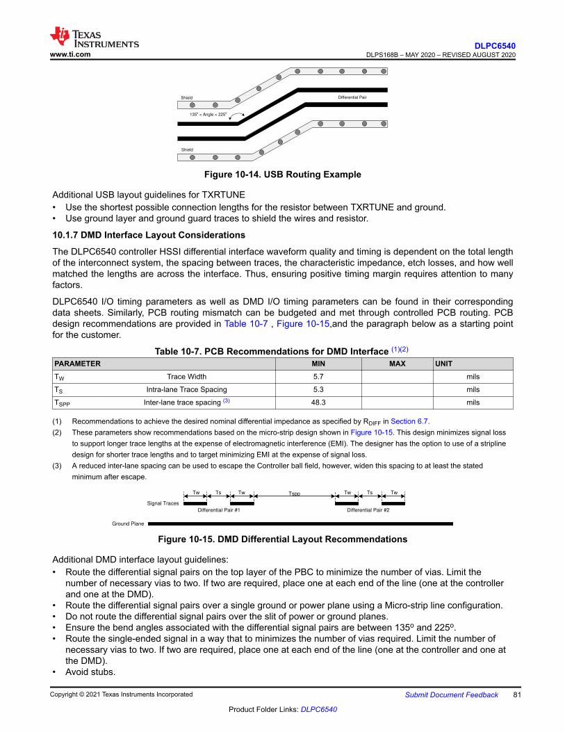
135o < Angle < 225o
Shield Differential Pair
Shield
Figure 10-14. USB Routing Example
Additional USB layout guidelines for TXRTUNE• Use the shortest possible connection lengths for the resistor between TXRTUNE and ground.• Use ground layer and ground guard traces to shield the wires and resistor.
10.1.7 DMD Interface Layout Considerations
The DLPC6540 controller HSSI differential interface waveform quality and timing is dependent on the total lengthof the interconnect system, the spacing between traces, the characteristic impedance, etch losses, and how wellmatched the lengths are across the interface. Thus, ensuring positive timing margin requires attention to manyfactors.
DLPC6540 I/O timing parameters as well as DMD I/O timing parameters can be found in their correspondingdata sheets. Similarly, PCB routing mismatch can be budgeted and met through controlled PCB routing. PCBdesign recommendations are provided in Table 10-7 , Figure 10-15,and the paragraph below as a starting pointfor the customer.
Table 10-7. PCB Recommendations for DMD Interface (1)(2) PARAMETER MIN MAX UNITTW Trace Width 5.7 mils
TS Intra-lane Trace Spacing 5.3 mils
TSPP Inter-lane trace spacing (3) 48.3 mils
(1) Recommendations to achieve the desired nominal differential impedance as specified by RDIFF in Section 6.7.(2) These parameters show recommendations based on the micro-strip design shown in Figure 10-15. This design minimizes signal loss
to support longer trace lengths at the expense of electromagnetic interference (EMI). The designer has the option to use of a striplinedesign for shorter trace lengths and to target minimizing EMI at the expense of signal loss.
(3) A reduced inter-lane spacing can be used to escape the Controller ball field, however, widen this spacing to at least the statedminimum after escape.
Tw Tw Tw TwTspp
Ground Plane
Signal Traces
Ts Ts
Differential Pair #1 Differential Pair #2
Figure 10-15. DMD Differential Layout Recommendations
Additional DMD interface layout guidelines:• Route the differential signal pairs on the top layer of the PBC to minimize the number of vias. Limit the
number of necessary vias to two. If two are required, place one at each end of the line (one at the controllerand one at the DMD).
• Route the differential signal pairs over a single ground or power plane using a Micro-strip line configuration.• Do not route the differential signal pairs over the slit of power or ground planes.• Ensure the bend angles associated with the differential signal pairs are between 135o and 225o.• Route the single-ended signal in a way that to minimizes the number of vias required. Limit the number of
necessary vias to two. If two are required, place one at each end of the line (one at the controller and one atthe DMD).
• Avoid stubs.
www.ti.comDLPC6540
DLPS168B – MAY 2020 – REVISED AUGUST 2020
Copyright © 2021 Texas Instruments Incorporated Submit Document Feedback 81
Product Folder Links: DLPC6540
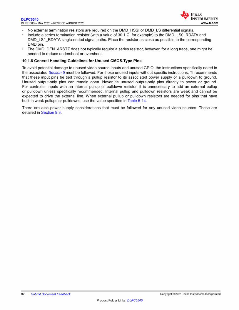
• No external termination resistors are required on the DMD_HSSI or DMD_LS differential signals.• Include a series termination resistor (with a value of 30.1 Ω, for example) to the DMD_LS0_RDATA and
DMD_LS1_RDATA single-ended signal paths. Place the resistor as close as possible to the correspondingDMD pin.
• The DMD_DEN_ARSTZ does not typically require a series resistor, however, for a long trace, one might beneeded to reduce undershoot or overshoot.
10.1.8 General Handling Guidelines for Unused CMOS-Type Pins
To avoid potential damage to unused video source inputs and unused GPIO, the instructions specifically noted inthe associated Section 5 must be followed. For those unused inputs without specific instructions, TI recommendsthat these input pins be tied through a pullup resistor to its associated power supply or a pulldown to ground.Unused output-only pins can remain open. Never tie unused output-only pins directly to power or ground.For controller inputs with an internal pullup or pulldown resistor, it is unnecessary to add an external pullupor pulldown unless specifically recommended. Internal pullup and pulldown resistors are weak and cannot beexpected to drive the external line. When external pullup or pulldown resistors are needed for pins that havebuilt-in weak pullups or pulldowns, use the value specified in Table 5-14.
There are also power supply considerations that must be followed for any unused video sources. These aredetailed in Section 9.3.
DLPC6540DLPS168B – MAY 2020 – REVISED AUGUST 2020 www.ti.com
82 Submit Document Feedback Copyright © 2021 Texas Instruments Incorporated
Product Folder Links: DLPC6540

10.1.9 Maximum Pin-to-Pin, PCB Interconnects Etch Lengths
Table 10-8. Max Pin-to-Pin PCB Interconnect Recommendations - DMDController INTERFACE SIGNAL INTERCONNECT TOPOLOGY (1) (2) (3)
UNITDMD SINGLE BOARD SIGNAL ROUTING
LENGTHMULTI-BOARD SIGNAL ROUTING
LENGTH
DMD_HSSI0_CLK_PDMD_HSSI0_CLK_N 10 (254)
Controller PCB: 2 (50.8)DMD PCB: 4 (101.6)
Flex: 10 (254)inch (mm)
DMD_HSSI0_D0_PDMD_HSSI0_D0_N
10 (254)Controller PCB: 2 (50.8)
DMD PCB: 4 (101.6)Flex: 10 (254)
inch (mm)
DMD_HSSI0_D1_PDMD_HSSI0_D1_N
DMD_HSSI0_D2_PDMD_HSSI0_D2_N
DMD_HSSI0_D3_PDMD_HSSI0_D3_N
DMD_HSSI0_D4_PDMD_HSSI0_D4_N
DMD_HSSI0_D5_PDMD_HSSI0_D5_N
DMD_HSSI0_D6_PDMD_HSSI0_D6_N
DMD_HSSI0_D7_PDMD_HSSI0_D7_N
DMD_HSSI1_CLK_PDMD_HSSI1_CLK_N 10 (254)
Controller PCB: 2 (50.8)DMD PCB: 4 (101.6)
Flex: 10 (254)inch (mm)
DMD_HSSI1_D0_PDMD_HSSI1_D0_N
10 (254)Controller PCB: 2 (50.8)
DMD PCB: 4 (101.6)Flex: 10 (254)
inch (mm)
DMD_HSSI1_D1_PDMD_HSSI1_D1_N
DMD_HSSI1_D2_PDMD_HSSI1_D2_N
DMD_HSSI1_D3_PDMD_HSSI1_D3_N
DMD_HSSI1_D4_PDMD_HSSI1_D4_N
DMD_HSSI1_D5_PDMD_HSSI1_D5_N
DMD_HSSI1_D6_PDMD_HSSI1_D6_N
DMD_HSSI1_D7_PDMD_HSSI1_D7_N
DMD_LS0_CLK_PDMD_LS0_CLK_N
18(457.2)
18(457.2)
inch(mm)
DMD_LS0_WDATA_PDMD_LS0_WDATA_N
18(457.2)
18(457.2)
inch(mm)
DMD_LS1_CLK_PDMD_LS1_CLK_N
18(457.2)
18(457.2)
inch(mm)
DMD_LS1_WDATA_PDMD_LS1_WDATA_N
18(457.2)
18(457.2)
inch(mm)
DMD_LS0_RDATA 18(457.2)
18(457.2)
inch(mm)
DMD_LS1_RDATA 18(457.2)
18(457.2)
inch(mm)
www.ti.comDLPC6540
DLPS168B – MAY 2020 – REVISED AUGUST 2020
Copyright © 2021 Texas Instruments Incorporated Submit Document Feedback 83
Product Folder Links: DLPC6540
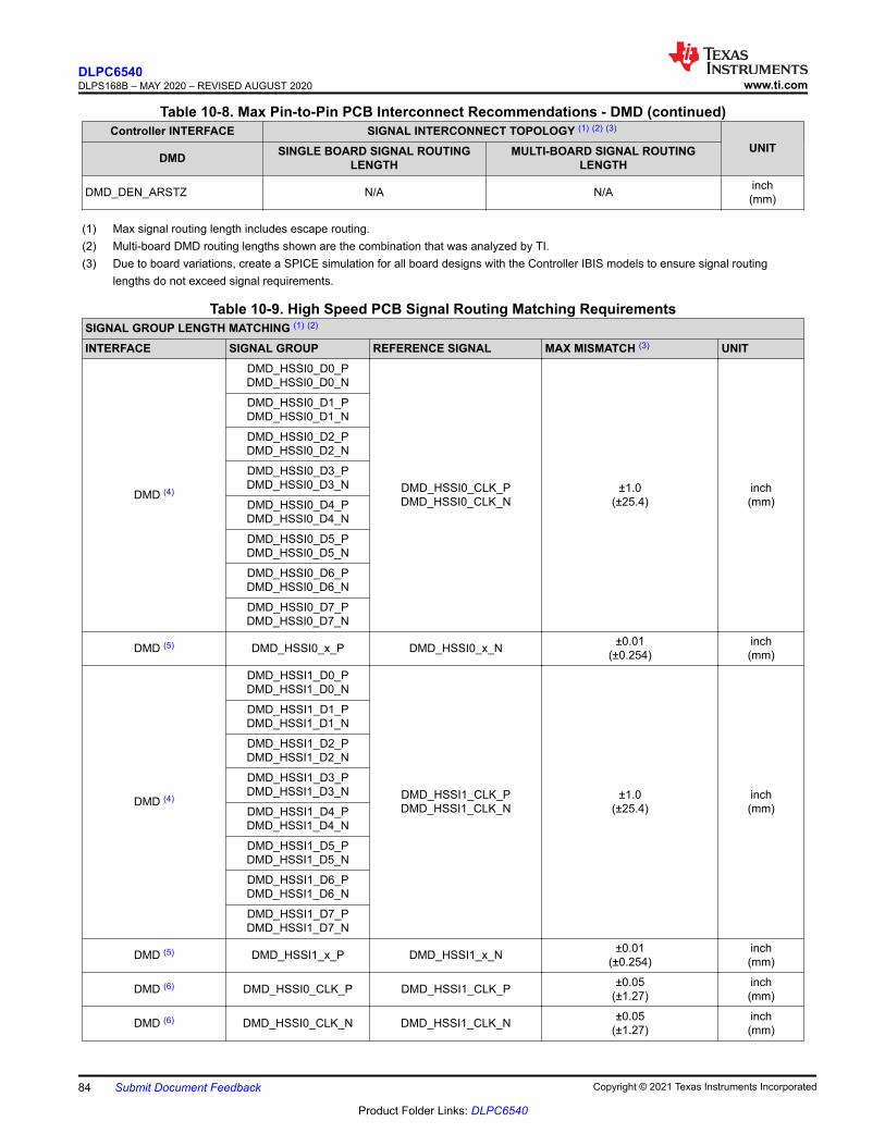
Table 10-8. Max Pin-to-Pin PCB Interconnect Recommendations - DMD (continued)Controller INTERFACE SIGNAL INTERCONNECT TOPOLOGY (1) (2) (3)
UNITDMD SINGLE BOARD SIGNAL ROUTING
LENGTHMULTI-BOARD SIGNAL ROUTING
LENGTH
DMD_DEN_ARSTZ N/A N/A inch(mm)
(1) Max signal routing length includes escape routing.(2) Multi-board DMD routing lengths shown are the combination that was analyzed by TI.(3) Due to board variations, create a SPICE simulation for all board designs with the Controller IBIS models to ensure signal routing
lengths do not exceed signal requirements.
Table 10-9. High Speed PCB Signal Routing Matching RequirementsSIGNAL GROUP LENGTH MATCHING (1) (2)
INTERFACE SIGNAL GROUP REFERENCE SIGNAL MAX MISMATCH (3) UNIT
DMD (4)
DMD_HSSI0_D0_PDMD_HSSI0_D0_N
DMD_HSSI0_CLK_PDMD_HSSI0_CLK_N
±1.0(±25.4)
inch(mm)
DMD_HSSI0_D1_PDMD_HSSI0_D1_N
DMD_HSSI0_D2_PDMD_HSSI0_D2_N
DMD_HSSI0_D3_PDMD_HSSI0_D3_N
DMD_HSSI0_D4_PDMD_HSSI0_D4_N
DMD_HSSI0_D5_PDMD_HSSI0_D5_N
DMD_HSSI0_D6_PDMD_HSSI0_D6_N
DMD_HSSI0_D7_PDMD_HSSI0_D7_N
DMD (5) DMD_HSSI0_x_P DMD_HSSI0_x_N ±0.01(±0.254)
inch(mm)
DMD (4)
DMD_HSSI1_D0_PDMD_HSSI1_D0_N
DMD_HSSI1_CLK_PDMD_HSSI1_CLK_N
±1.0(±25.4)
inch(mm)
DMD_HSSI1_D1_PDMD_HSSI1_D1_N
DMD_HSSI1_D2_PDMD_HSSI1_D2_N
DMD_HSSI1_D3_PDMD_HSSI1_D3_N
DMD_HSSI1_D4_PDMD_HSSI1_D4_N
DMD_HSSI1_D5_PDMD_HSSI1_D5_N
DMD_HSSI1_D6_PDMD_HSSI1_D6_N
DMD_HSSI1_D7_PDMD_HSSI1_D7_N
DMD (5) DMD_HSSI1_x_P DMD_HSSI1_x_N ±0.01(±0.254)
inch(mm)
DMD (6) DMD_HSSI0_CLK_P DMD_HSSI1_CLK_P ±0.05(±1.27)
inch(mm)
DMD (6) DMD_HSSI0_CLK_N DMD_HSSI1_CLK_N ±0.05(±1.27)
inch(mm)
DLPC6540DLPS168B – MAY 2020 – REVISED AUGUST 2020 www.ti.com
84 Submit Document Feedback Copyright © 2021 Texas Instruments Incorporated
Product Folder Links: DLPC6540

Table 10-9. High Speed PCB Signal Routing Matching Requirements (continued)SIGNAL GROUP LENGTH MATCHING (1) (2)
INTERFACE SIGNAL GROUP REFERENCE SIGNAL MAX MISMATCH (3) UNIT
DMD (4) DMD_LS0_WDATA_PDMD_LS0_WDATA_N
DMD_LS0_CLK_PDMD_LS0_CLK_N
±1.0(±25.4)
inch(mm)
DMD (5) DMD_LS0_x_P DMD_LS0_x_N ±0.025(±0.635)
inch(mm)
DMD (4) DMD_LS1_WDATA_PDMD_LS1_WDATA_N
DMD_LS1_CLK_PDMD_LS1_CLK_N
±1.0(±25.4)
inch(mm)
DMD (5) DMD_LS1_x_P DMD_LS1_x_N ±0.025(±0.635)
inch(mm)
DMD DMD_LS0_RDATADMD_LS1_RDATA N/A N/A (7) inch
(mm)
DMD DMD_DEN_ARSTZ N/A N/A inch(mm)
(1) These routing requirements are specific to the PCB routing. Internal package routing mismatches in the DLPC6540 and DLP471TPhave already been accounted for in these requirements.
(2) Training is applied to DMD HS data lines, so defined matching requirements are slightly relaxed.(3) This requirement must be maintained from the Controller to the DMD, even if the signals traverse multiple boards.(4) This is an inter-pair specification (that is, differential pair to differential pair within the group).(5) This is an intra-pair specification (that is, length mismatch between P and N for the same pair). This is applicable to both clock and
data.(6) This is a channel to channel skew specification.(7) The low speed read control interface from the DMD is single ended, and makes use of the differential write clock. As such, a routing
mismatch between these is not applicable.
10.2 Thermal ConsiderationsThe underlying thermal requirement for the DLPC6540 is that the maximum operating junction temperature (TJ)not be exceeded (defined in the Section 6.3). This temperature is dependent on operating ambient temperature,heatsink, airflow, PCB design (including the component layout density and the amount of copper used), powerdissipation of the DLPC6540, and power dissipation of surrounding components. The DLPC6540’s package isdesigned to extract heat via the package heat slug to the heatsink, via the thermal balls, and through the powerand ground planes of the PCB. Thus, heatsink, copper content, and airflow over the PCB are important factors.
The recommended maximum operating ambient temperature (TA) is provided primarily as a design target and isbased on maximum DLPC6540 power dissipation and RθJA at 0 m/s,1 m/s, and 2 m/s of forced airflow, whereRθJA is the thermal resistance of the package as measured using the test board described in Section 10.1.1.This test PCB is not necessarily representative of the customers PCB and thus the reported thermal resistancecan differ from the actual product application. Although the actual thermal resistance can be different, it is thebest information available during the design phase to estimate thermal performance. TI highly recommends thatonce the host PCB is designed and built that the thermal performance be measured and validated.
To do this, measure the top center case temperature under the worse case product scenario (max powerdissipation, max voltage, max ambient temperature) and validate that the maximum recommended casetemperature (TC) is not exceeded. This specification is based on the measured φJT for the DLPC6540 packageand provides a relatively accurate correlation to junction temperature. Take care when measuring this casetemperature to prevent accidental cooling of the package surface. TI recommends a small (approximately 40gauge) thermocouple. Ensure that the bead and thermocouple wire contact the top of the package. Cover thebead and thermocouple wire with a minimal amount of thermally conductive epoxy. Route the wires closely alongthe package and the board surface to avoid cooling the bead through the wires.
www.ti.comDLPC6540
DLPS168B – MAY 2020 – REVISED AUGUST 2020
Copyright © 2021 Texas Instruments Incorporated Submit Document Feedback 85
Product Folder Links: DLPC6540

11 Device and Documentation Support11.1 Device Support11.1.1 Third-Party Products Disclaimer
TI'S PUBLICATION OF INFORMATION REGARDING THIRD-PARTY PRODUCTS OR SERVICES DOES NOTCONSTITUTE AN ENDORSEMENT REGARDING THE SUITABILITY OF SUCH PRODUCTS OR SERVICESOR A WARRANTY, REPRESENTATION OR ENDORSEMENT OF SUCH PRODUCTS OR SERVICES, EITHERALONE OR IN COMBINATION WITH ANY TI PRODUCT OR SERVICE.
11.1.2 Device Nomenclature11.1.2.1 Device Markings
Terminal A1 corner
1
3
2
TEXAS INSTRUMENTS
DLP®
XDLPC6540ZDC
XXXXXXXX-XXXXXX
CCCCCC YYWW
LLLLL TTTT G1 4
Marking Definitions:
Line 1: TI Part Number: EngineeringSamples
X = Engineering Samples DLPC6540 = Device ID blank or A, B, C ... = Part Revision ZDC = Package designator
TI Part Number: Production DLPC6540 = Device ID blank or A, B, C ... = Part Revision ZDC = Package designator
Line 2: Vendor Information XXXXXXX-XXXXXX
Line 3:Vendor Country Year and Weekcode
CCCCCC = Country YY = Year WW = Week
Line 4: Vendor Lot and Trace Code LLLLL = Lot code TTTT = Trace code
11.1.2.2 Package Data
Table 11-1. Package InformationPARAMETER VALUE UNITS
Number of balls (signal/thermal) 612 / 64
Ball pitch 1.00 mm
UBM (under bump metallurgy) 0.48 (See Figure 11-1) mm
BPD (ball pad diameter) 0.58 (See Figure 11-1) mm
Body dimension See Mechanical Drawing mm
Mold compound dimensions See Mechanical Drawing mm
Package volume class 350 - 2000 (J-STD-20D) mm3
Approximate weight 5.64 g
Substrate circuit Pb-free
Package balls Pb-free
Solder paste Pb-free
DLPC6540DLPS168B – MAY 2020 – REVISED AUGUST 2020 www.ti.com
86 Submit Document Feedback Copyright © 2021 Texas Instruments Incorporated
Product Folder Links: DLPC6540
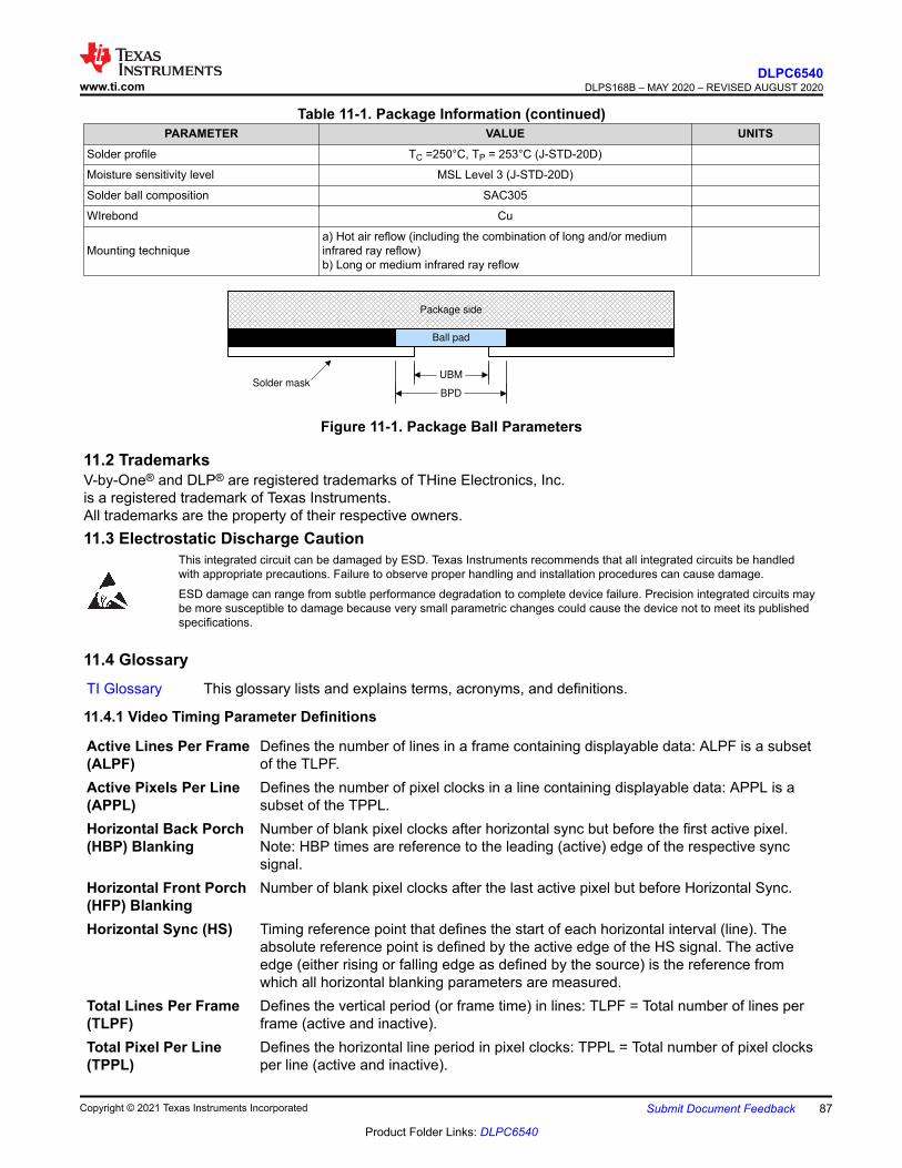
Table 11-1. Package Information (continued)PARAMETER VALUE UNITS
Solder profile TC =250°C, TP = 253°C (J-STD-20D)
Moisture sensitivity level MSL Level 3 (J-STD-20D)
Solder ball composition SAC305
WIrebond Cu
Mounting techniquea) Hot air reflow (including the combination of long and/or mediuminfrared ray reflow)b) Long or medium infrared ray reflow
UBM
Ball pad
Solder mask BPD.
UBM.
Package side
Figure 11-1. Package Ball Parameters
11.2 TrademarksV-by-One® and DLP® are registered trademarks of THine Electronics, Inc.is a registered trademark of Texas Instruments.All trademarks are the property of their respective owners.11.3 Electrostatic Discharge Caution
This integrated circuit can be damaged by ESD. Texas Instruments recommends that all integrated circuits be handledwith appropriate precautions. Failure to observe proper handling and installation procedures can cause damage.ESD damage can range from subtle performance degradation to complete device failure. Precision integrated circuits maybe more susceptible to damage because very small parametric changes could cause the device not to meet its publishedspecifications.
11.4 GlossaryTI Glossary This glossary lists and explains terms, acronyms, and definitions.
11.4.1 Video Timing Parameter Definitions
Active Lines Per Frame(ALPF)
Defines the number of lines in a frame containing displayable data: ALPF is a subsetof the TLPF.
Active Pixels Per Line(APPL)
Defines the number of pixel clocks in a line containing displayable data: APPL is asubset of the TPPL.
Horizontal Back Porch(HBP) Blanking
Number of blank pixel clocks after horizontal sync but before the first active pixel.Note: HBP times are reference to the leading (active) edge of the respective syncsignal.
Horizontal Front Porch(HFP) Blanking
Number of blank pixel clocks after the last active pixel but before Horizontal Sync.
Horizontal Sync (HS) Timing reference point that defines the start of each horizontal interval (line). Theabsolute reference point is defined by the active edge of the HS signal. The activeedge (either rising or falling edge as defined by the source) is the reference fromwhich all horizontal blanking parameters are measured.
Total Lines Per Frame(TLPF)
Defines the vertical period (or frame time) in lines: TLPF = Total number of lines perframe (active and inactive).
Total Pixel Per Line(TPPL)
Defines the horizontal line period in pixel clocks: TPPL = Total number of pixel clocksper line (active and inactive).
www.ti.comDLPC6540
DLPS168B – MAY 2020 – REVISED AUGUST 2020
Copyright © 2021 Texas Instruments Incorporated Submit Document Feedback 87
Product Folder Links: DLPC6540

Vertical Sync (VS) Timing reference point that defines the start of the vertical interval (frame). Theabsolute reference point is defined by the active edge of the VS signal. The activeedge (either rising or falling edge as defined by the source) is the reference fromwhich all vertical blanking parameters are measured.
Vertical Back Porch(VBP) Blanking
Number of blank lines after vertical sync but before the first active line.
Vertical Front Porch(VFP) Blanking
Number of blank lines after the last active line but before vertical sync.
Vertical Back Porch (VBP)
Vertical Front Porch (VFP)
Horizontal
Back
Porch
(HBP)
Horizontal
Front
Porch
(HFP)
TLPF
TPPL
APPL
ALPF
DLPC6540DLPS168B – MAY 2020 – REVISED AUGUST 2020 www.ti.com
88 Submit Document Feedback Copyright © 2021 Texas Instruments Incorporated
Product Folder Links: DLPC6540

12 Mechanical, Packaging, and Orderable InformationThe following pages include mechanical, packaging, and orderable information. This information is the mostcurrent data available for the designated devices. This data is subject to change without notice and revision ofthis document. For browser-based versions of this data sheet, refer to the left-hand navigation.
www.ti.comDLPC6540
DLPS168B – MAY 2020 – REVISED AUGUST 2020
Copyright © 2021 Texas Instruments Incorporated Submit Document Feedback 89
Product Folder Links: DLPC6540

12.1 Package Option Addendum
DLPC6540DLPS168B – MAY 2020 – REVISED AUGUST 2020 www.ti.com
90 Submit Document Feedback Copyright © 2021 Texas Instruments Incorporated
Product Folder Links: DLPC6540

PACKAGE OPTION ADDENDUM
www.ti.com 17-Jul-2021
Addendum-Page 1
PACKAGING INFORMATION
Orderable Device Status(1)
Package Type PackageDrawing
Pins PackageQty
Eco Plan(2)
Lead finish/Ball material
(6)
MSL Peak Temp(3)
Op Temp (°C) Device Marking(4/5)
Samples
DLPC6540ZDC ACTIVE BGA ZDC 676 27 TBD Call TI Call TI 0 to 70
(1) The marketing status values are defined as follows:ACTIVE: Product device recommended for new designs.LIFEBUY: TI has announced that the device will be discontinued, and a lifetime-buy period is in effect.NRND: Not recommended for new designs. Device is in production to support existing customers, but TI does not recommend using this part in a new design.PREVIEW: Device has been announced but is not in production. Samples may or may not be available.OBSOLETE: TI has discontinued the production of the device.
(2) RoHS: TI defines "RoHS" to mean semiconductor products that are compliant with the current EU RoHS requirements for all 10 RoHS substances, including the requirement that RoHS substancedo not exceed 0.1% by weight in homogeneous materials. Where designed to be soldered at high temperatures, "RoHS" products are suitable for use in specified lead-free processes. TI mayreference these types of products as "Pb-Free".RoHS Exempt: TI defines "RoHS Exempt" to mean products that contain lead but are compliant with EU RoHS pursuant to a specific EU RoHS exemption.Green: TI defines "Green" to mean the content of Chlorine (Cl) and Bromine (Br) based flame retardants meet JS709B low halogen requirements of <=1000ppm threshold. Antimony trioxide basedflame retardants must also meet the <=1000ppm threshold requirement.
(3) MSL, Peak Temp. - The Moisture Sensitivity Level rating according to the JEDEC industry standard classifications, and peak solder temperature.
(4) There may be additional marking, which relates to the logo, the lot trace code information, or the environmental category on the device.
(5) Multiple Device Markings will be inside parentheses. Only one Device Marking contained in parentheses and separated by a "~" will appear on a device. If a line is indented then it is a continuationof the previous line and the two combined represent the entire Device Marking for that device.
(6) Lead finish/Ball material - Orderable Devices may have multiple material finish options. Finish options are separated by a vertical ruled line. Lead finish/Ball material values may wrap to twolines if the finish value exceeds the maximum column width.
Important Information and Disclaimer:The information provided on this page represents TI's knowledge and belief as of the date that it is provided. TI bases its knowledge and belief on informationprovided by third parties, and makes no representation or warranty as to the accuracy of such information. Efforts are underway to better integrate information from third parties. TI has taken andcontinues to take reasonable steps to provide representative and accurate information but may not have conducted destructive testing or chemical analysis on incoming materials and chemicals.TI and TI suppliers consider certain information to be proprietary, and thus CAS numbers and other limited information may not be available for release.
In no event shall TI's liability arising out of such information exceed the total purchase price of the TI part(s) at issue in this document sold by TI to Customer on an annual basis.

www.ti.com
PACKAGE OUTLINE
C2.40 MAX
0.60.4 TYP
29TYP
29 TYP
1 TYP
1 TYP
676X 0.70.5
A 31.130.9
B
31.130.9
(1) TYP
(1) TYP
( 29)
( 23)HEAT SLUG
(1.17)
4224809/A 02/2019
PBGA - 2.4 mm max heightZDC0676APLASTIC BALL GRID ARRAY
NOTES: 1. All linear dimensions are in millimeters. Any dimensions in parenthesis are for reference only. Dimensioning and tolerancing per ASME Y14.5M. 2. This drawing is subject to change without notice.
CDEFGHJKLMNPRTUVWY
AAABACADAEAFAGAHAJ
AK
BALL A1 CORNER
4X (45 X 0.2)
SEATING PLANEBALL TYP 0.2 C
0.35 C
12
3
0.25 C A B0.1 C
SYMM
SYMM
45
67
89
1011
1213
1415
1617
1819
2021
2223
2425
A27
26 28
B
2930
SCALE 0.500
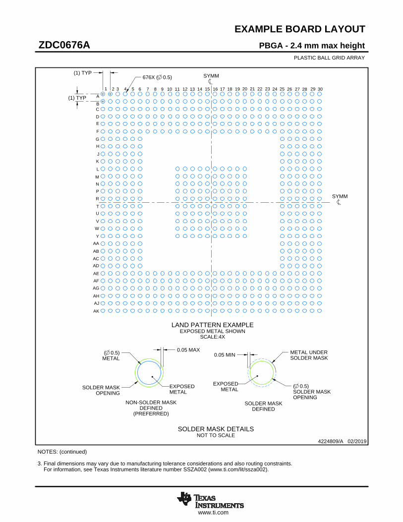
www.ti.com
EXAMPLE BOARD LAYOUT
676X ( 0.5)(1) TYP
(1) TYP
( 0.5)METAL
0.05 MAX
SOLDER MASKOPENING
METAL UNDERSOLDER MASK
( 0.5)SOLDER MASKOPENING
0.05 MIN
4224809/A 02/2019
PBGA - 2.4 mm max heightZDC0676APLASTIC BALL GRID ARRAY
NOTES: (continued) 3. Final dimensions may vary due to manufacturing tolerance considerations and also routing constraints. For information, see Texas Instruments literature number SSZA002 (www.ti.com/lit/ssza002).
SYMM
SYMM
LAND PATTERN EXAMPLEEXPOSED METAL SHOWN
SCALE:4X
1 2 3 4 5 6 7 8 9 10 11 12 13 14 15 16 17 18 19 20 21 22 23 24 25A
26 27 28 29 30
BC
DE
F
GH
JK
L
MNP
R
TU
VW
YAA
AB
ACAD
AEAFAG
AHAJ
AK
NON-SOLDER MASKDEFINED
(PREFERRED)
SOLDER MASK DETAILSNOT TO SCALE
EXPOSEDMETAL
SOLDER MASKDEFINED
EXPOSEDMETAL

www.ti.com
EXAMPLE STENCIL DESIGN
(1) TYP
(1) TYP
676X ( 0.5)
4224809/A 02/2019
PBGA - 2.4 mm max heightZDC0676APLASTIC BALL GRID ARRAY
NOTES: (continued) 5. Laser cutting apertures with trapezoidal walls and rounded corners may offer better paste release.
SOLDER PASTE EXAMPLEBASED ON 0.15 mm THICK STENCIL
SCALE: 4X
1 2 3 4 5 6 7 8 9 10 11 12 13 14 15 16 17 18 19 20 21 22 23 24 25 26 27 28 29 30A
BC
DE
F
GH
JK
L
MNP
R
TU
VW
YAA
AB
ACAD
AEAFAG
AHAJ
AK

IMPORTANT NOTICE AND DISCLAIMERTI PROVIDES TECHNICAL AND RELIABILITY DATA (INCLUDING DATASHEETS), DESIGN RESOURCES (INCLUDING REFERENCEDESIGNS), APPLICATION OR OTHER DESIGN ADVICE, WEB TOOLS, SAFETY INFORMATION, AND OTHER RESOURCES “AS IS”AND WITH ALL FAULTS, AND DISCLAIMS ALL WARRANTIES, EXPRESS AND IMPLIED, INCLUDING WITHOUT LIMITATION ANYIMPLIED WARRANTIES OF MERCHANTABILITY, FITNESS FOR A PARTICULAR PURPOSE OR NON-INFRINGEMENT OF THIRDPARTY INTELLECTUAL PROPERTY RIGHTS.These resources are intended for skilled developers designing with TI products. You are solely responsible for (1) selecting the appropriateTI products for your application, (2) designing, validating and testing your application, and (3) ensuring your application meets applicablestandards, and any other safety, security, or other requirements. These resources are subject to change without notice. TI grants youpermission to use these resources only for development of an application that uses the TI products described in the resource. Otherreproduction and display of these resources is prohibited. No license is granted to any other TI intellectual property right or to any third partyintellectual property right. TI disclaims responsibility for, and you will fully indemnify TI and its representatives against, any claims, damages,costs, losses, and liabilities arising out of your use of these resources.TI’s products are provided subject to TI’s Terms of Sale (https:www.ti.com/legal/termsofsale.html) or other applicable terms available eitheron ti.com or provided in conjunction with such TI products. TI’s provision of these resources does not expand or otherwise alter TI’sapplicable warranties or warranty disclaimers for TI products.IMPORTANT NOTICE
Mailing Address: Texas Instruments, Post Office Box 655303, Dallas, Texas 75265Copyright © 2021, Texas Instruments Incorporated

Mouser Electronics
Authorized Distributor
Click to View Pricing, Inventory, Delivery & Lifecycle Information: Texas Instruments:
DLPC6540ZDC