dissertation_thuermer.pdf - Heidelberg University
238
DISSERTATION submitted to the Combined Faculty for the Natural Sciences and Mathematics of Heidelberg University, Germany for the degree of Doctor of Natural Sciences Put forward by Dipl.Phys. Dipl.Inf. Maximilian Thürmer Born in Heidelberg on August 31st, 1983 Date of oral examination: ________________________
-
Upload
khangminh22 -
Category
Documents
-
view
1 -
download
0
Transcript of dissertation_thuermer.pdf - Heidelberg University

DISSERTATION
submitted
to the
Combined Faculty for the Natural Sciences and Mathematics
of
Heidelberg University, Germany
for the degree of
Doctor of Natural Sciences
Put forward by
Dipl.Phys. Dipl.Inf. Maximilian Thürmer
Born in Heidelberg on August 31st, 1983
Date of oral examination: ________________________

Modelling and performance analysis ofmultigigabit serial interconnects using realnumber based analog verification methods
Advisor: Prof. Dr. Ulrich Brüning


Danksagungen
Wissenschaftlich gesehen mögen wir alle auf den Schultern von Giganten stehen, dochselbst dieser aufrechte Stand ist uns nur möglich, dank der uns liebenden Menschen, diesich um uns sorgen und Worte der Empathie für uns in den Phasen finden, in denen wir sieam nötigsten haben.
Daher danke ich meiner Familie aus vollem Herzen für all ihre Unterstützung, besonderswährend der fordernden letzten Monate. Dies gilt im höchsten Maße meiner Frau undmeiner Tochter, die mich für diese Zeit so oft haben entbehren müssen und ohne derenliebevolle Fürsorge und Aufmunterungen diese Arbeit schlicht nicht möglich gewesenwäre. Dank gilt auch meinen Eltern und deren Partner, meiner Schwester und deren Familiesowie meiner Schwiegermutter für die zahllosen guten Gespräche und Aufmunterungensowie deren fortwährendes Interesse am Fortschritt meiner Arbeit.
Ebenso danke ich meinen Kollegen, inmitten und mit Hilfe derer diese Arbeit entstandenist. Dies gilt besonders für die enge Zusammenarbeit mit Markus Müller, aber ebenso fürdie anderen Mitglieder unseres kleinen, aber sehr engagierten Teams, in dem die zahllosenDiskussionen, die zu führen waren, stets zu produktiven und kreativen Ideen inspirierten.
Abschließend gilt mein Dank Herrn Prof. Dr. Brüning für die Möglichkeit, dieseArbeit anzufertigen sowie für sein stets offenes Ohr und die anregenden, fachlichenDiskussionen.

Contents
1 Introduction 1
1.1 Challenges in contemporary design and analysis methodologies . . . . . . 4
1.2 Structure of this work . . . . . . . . . . . . . . . . . . . . . . . . . . . . . . 7
2 Electrical serializer based multi-gigabit communication links 9
2.1 Mathematical definitions and relations . . . . . . . . . . . . . . . . . . . . . 9
2.2 Link system overview and nomenclature . . . . . . . . . . . . . . . . . . . 12
2.2.1 The bit error rate . . . . . . . . . . . . . . . . . . . . . . . . . . . . 13
2.2.2 Interaction with higher communication layers . . . . . . . . . . . . 17
2.2.3 Power distribution . . . . . . . . . . . . . . . . . . . . . . . . . . . 21
2.2.4 Phase locked loop . . . . . . . . . . . . . . . . . . . . . . . . . . . . 24
2.2.5 Transmitter . . . . . . . . . . . . . . . . . . . . . . . . . . . . . . . . 31
2.2.6 Receiver . . . . . . . . . . . . . . . . . . . . . . . . . . . . . . . . . 34
2.2.6.1 Clock data recovery circuit . . . . . . . . . . . . . . . . 35
3 Electrical transmission channels and equalization 41
3.1 The bitrate capacity . . . . . . . . . . . . . . . . . . . . . . . . . . . . . . . 44
3.2 Performance regions and the Johnson Signal Model . . . . . . . . . . . . . 46
3.2.1 Lumped Element Region . . . . . . . . . . . . . . . . . . . . . . . . 48
3.2.2 RC Region . . . . . . . . . . . . . . . . . . . . . . . . . . . . . . . . 49
3.2.3 LC Region . . . . . . . . . . . . . . . . . . . . . . . . . . . . . . . . 50
3.2.4 Skin-effect Region . . . . . . . . . . . . . . . . . . . . . . . . . . . 50
3.2.5 Dielectric loss Region . . . . . . . . . . . . . . . . . . . . . . . . . 51
3.2.6 Waveguide dispersion region . . . . . . . . . . . . . . . . . . . . . 52
3.2.7 Johnson Signal Model for a coaxial transmission line . . . . . . . 52
3.3 Equalization techniques . . . . . . . . . . . . . . . . . . . . . . . . . . . . . 65
3.3.1 Finite impulse response filter . . . . . . . . . . . . . . . . . . . . . 65
3.3.2 Continuous time linear equalizer . . . . . . . . . . . . . . . . . . . 68
3.3.3 Decision feedback equalization . . . . . . . . . . . . . . . . . . . . 70
3.3.4 Equalizer adaption . . . . . . . . . . . . . . . . . . . . . . . . . . . 73
3.4 Line Coding and power spectral density . . . . . . . . . . . . . . . . . . . . 76
vii
viii Contents
4 Serializer system component modelling 81
4.1 General Real Number Modelling Considerations . . . . . . . . . . . . . . . 85
4.2 The openMGT framework . . . . . . . . . . . . . . . . . . . . . . . . . . . 91
4.2.1 Leaf cells . . . . . . . . . . . . . . . . . . . . . . . . . . . . . . . . . 92
4.2.2 Testbenches . . . . . . . . . . . . . . . . . . . . . . . . . . . . . . . 95
4.3 The openMGT C and Octave modelling extension (OCM) . . . . . . . . . 95
4.3.1 General architecture . . . . . . . . . . . . . . . . . . . . . . . . . . 96
4.3.2 Self consistency of testbench and model . . . . . . . . . . . . . . . 99
4.4 Channel modelling process . . . . . . . . . . . . . . . . . . . . . . . . . . . 101
4.4.1 OCM data preparation . . . . . . . . . . . . . . . . . . . . . . . . . 103
4.4.2 Optimized C convolution routine . . . . . . . . . . . . . . . . . . . 105
4.4.3 SystemVerilog considerations . . . . . . . . . . . . . . . . . . . . . 106
4.4.4 Testbench and performance comparison . . . . . . . . . . . . . . . 109
4.5 Sampler modelling process . . . . . . . . . . . . . . . . . . . . . . . . . . . 117
4.5.1 Model theory . . . . . . . . . . . . . . . . . . . . . . . . . . . . . . 120
4.5.2 Models / OCM Data Sources . . . . . . . . . . . . . . . . . . . . . 132
4.5.3 SystemVerilog considerations . . . . . . . . . . . . . . . . . . . . . 134
4.5.4 Optimized C modelling routine . . . . . . . . . . . . . . . . . . . . 135
4.5.5 Testbench and performance analysis . . . . . . . . . . . . . . . . . 135
5 Link budgeting 137
5.1 History and state of the art . . . . . . . . . . . . . . . . . . . . . . . . . . . 138
5.2 The Peak distortion analysis algorithm . . . . . . . . . . . . . . . . . . . . 145
5.3 The OCM link budgeting algorithm . . . . . . . . . . . . . . . . . . . . . . 152
5.3.1 Power distribution . . . . . . . . . . . . . . . . . . . . . . . . . . . 156
5.3.2 PLL phase noise spectral density for transmitter and receiver . . . 156
5.3.3 Peak distortion analysis . . . . . . . . . . . . . . . . . . . . . . . . 157
5.3.4 System channel and jitter amplification in CDR based systems . . 158
5.3.5 System voltage noise estimation . . . . . . . . . . . . . . . . . . . 165
5.3.6 Clock data recovery and sampler phase noise estimation . . . . . 167
5.3.7 Final statistical eye compilation and metric extraction . . . . . . . 176
6 Design evaluation 179
6.1 A quarter rate serializer design . . . . . . . . . . . . . . . . . . . . . . . . . 179
6.2 Analysis of 10 Gigabit operation . . . . . . . . . . . . . . . . . . . . . . . . 182
6.3 Analysis of 20 Gbps operation . . . . . . . . . . . . . . . . . . . . . . . . . 188
6.4 Influence of the sampler ISF . . . . . . . . . . . . . . . . . . . . . . . . . . 191
6.5 Scaling channel geometry with the Johnson Signal Model . . . . . . . . . 193
7 Conclusion and Outlook 197

Contents ix
List of Figures 201
List of Tables 209
AppendixA 214
AppendixB 217

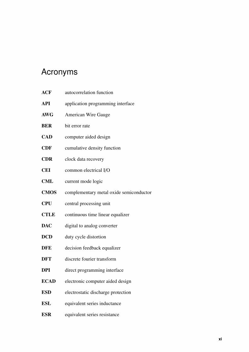
Acronyms
ACF autocorrelation function
API application programming interface
AWG American Wire Gauge
BER bit error rate
CAD computer aided design
CDF cumulative density function
CDR clock data recovery
CEI common electrical I/O
CML current mode logic
CMOS complementary metal oxide semiconductor
CPU central processing unit
CTLE continuous time linear equalizer
DAC digital to analog converter
DCD duty cycle distortion
DFE decision feedback equalizer
DFT discrete fourier transform
DPI direct programming interface
ECAD electronic computer aided design
ESD electrostatic discharge protection
ESL equivalent series inductance
ESR equivalent series resistance
xi

xii Contents
EVN equivalent voltage noise
FIR finite impulse response
HPC high performance computing
IC integrated circuit
ISF impulse sensitivity function
ISI intersymbol interference
LTI linear time invariant
NIC network interface controller
NRZ non return to zero
OCM openMGT modeling framework
OCD openMGT OCM data analysis and post processing backend
OIF Optical Internetworking Forum
PAM pulse amplitude modulation
PCB printed circuit board
PDA peak distortion analysis
PDF probability density function
PDK physical design kit
PDN power distribution network
PLL phase locked loop
PRBS pseudo random bit sequence
PSD power spectral density
PSRR power supply rejection ratio
RF radio frequency
RMS root-mean-square
RNM real number model
SBR single bit response

Contents xiii
SNR signal to noise ratio
SOC system on chip
VCO voltage controlled oscillator
VGA variable gain amplifier
VRM voltage regulator module

1 Introduction
Over the past decade there has been a strong trend towards serializer based multigigabitcommunication interfaces. While network interfaces between compute nodes have beenusing mutligigabit transmission for a long period of time already (10G Ethernet, Infiniband)and system interconnects between central processing unit (CPU) and peripheral (I/O)devices have entered the gigahertz region for quite a while, too (Hypertransport, QPI,PCI-E, S-ATA), the CPU to memory interconnects are the next domain to follow suit(HBM, HMC). This is also true for memory interfaces in the mobile processor segment[26]as well as for peripheral standards such as USB 3.0 or HDMI.
A serializer, also called transceiver or SERDES, is an electronic subsystem within anintegrated circuit (IC). It consists of a transmitting and a receiving part. The transmitteracts as a multiplexer (serializer) with an output driver for the transmission channel whilethe receiver implements a demultiplexer (deserializer) with analog input to digital outputconversion. Data is therefore modulated onto the channel or decoded from it at a higherfrequency than it is accepted from or presented to the parallel side interfacing with the chipfabric.
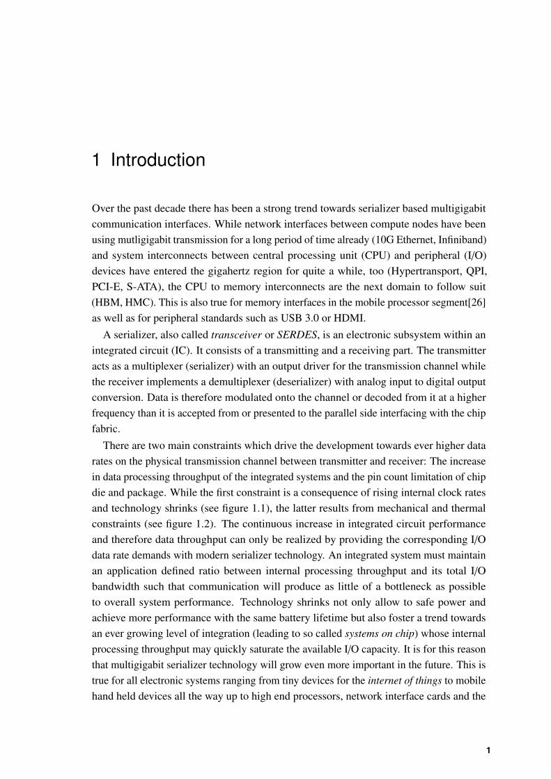
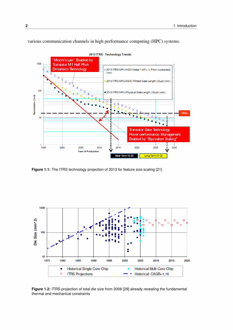
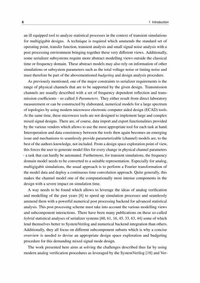
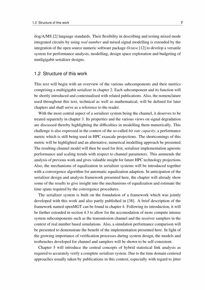
There are two main constraints which drive the development towards ever higher datarates on the physical transmission channel between transmitter and receiver: The increasein data processing throughput of the integrated systems and the pin count limitation of chipdie and package. While the first constraint is a consequence of rising internal clock ratesand technology shrinks (see figure 1.1), the latter results from mechanical and thermalconstraints (see figure 1.2). The continuous increase in integrated circuit performanceand therefore data throughput can only be realized by providing the corresponding I/Odata rate demands with modern serializer technology. An integrated system must maintainan application defined ratio between internal processing throughput and its total I/Obandwidth such that communication will produce as little of a bottleneck as possibleto overall system performance. Technology shrinks not only allow to safe power andachieve more performance with the same battery lifetime but also foster a trend towardsan ever growing level of integration (leading to so called systems on chip) whose internalprocessing throughput may quickly saturate the available I/O capacity. It is for this reasonthat multigigabit serializer technology will grow even more important in the future. This istrue for all electronic systems ranging from tiny devices for the internet of things to mobilehand held devices all the way up to high end processors, network interface cards and the
1
2 1 Introduction
various communication channels in high performance computing (HPC) systems.
Figure 1.1: The ITRS technology projection of 2013 for feature size scaling [21]
Figure 1.2: ITRS projection of total die size from 2008 [29] already revealing the fundamentalthermal and mechanical constraints

3
As previously noted, the frequency at which data is modulated onto the transmis-sion channel or extracted from it is related to the chip internal clock frequency via the(de)muxing ratio. This is unless more sophisticated data modulation schemes than standardnon-return to zero single data rate signalling are used. Serializer circuits are usuallyemployed to transfer information across distances far greater than that of the integratedcircuit itself. Especially in high performance computing applications, there is a greatvariety of transmission channels. The most challenging specimen realize intercabinet orinternode connections by using long copper cabling or backplane traces. Due to their highdielectric and conductor losses and the unavoidable signal degradation at every connector,all of which become worse as frequency increases, the transmitters and receivers have tocompensate these effects as much as possible. Output driver and analog receiver frontendwill therefore substantially grow in complexity and inevitably consume more power.
Equally challenging are chip to chip interconnects within a single node (computesystem), These interconnects can either be between different CPUs, between CPUs andperipheral devices or simply from CPU to main memory. The quality of copper cables ishigh compared to printed circuit board (PCB) traces and its dielectric and conductor lossescomparably low. Therefore, even though these node internal connections do not span asmuch of a distance, their malicious impact on signal quality is very significant even atshorter distances.
Another trend of past years has been to progress system integration whereever possible.This ranges from multi-die packages which may for instance combine processor andmemory modules [20, 43] to chip on chip packaging with through silicon vias [65].Despite these small distances, with the steady increase in signal frequencies to the highGigahertz range the resulting electromagnetic wavelenghts are still comparable or belowthe transmission line extents. The transmission channel will therefore have to be treatedand analyzed with microwave engineering approaches. Depending on operating frequency,this may be true for on-package interconnects - it certainly cannot be avoided for longercommunication channels of complex topology.
Regardless of application scope, a serializer system requires a broad span of analysisand implementation tools from various disciplines. Microwave engineering techniquesare required for channel and power distribution analysis alike. The output driver of thetransmitter and the signal preconditioning stages of the receiver are very broadband all-analog integrated building blocks. Also, the clocking sources and clock distribution schemeare to the largest degree an analog design effort. The multiplexing and demultiplexingstages on the other hand could be approached with either analog or semicustom, digitaldesign methods. As technologies continue to shrink, however, favouring the mostlyautomated semicustom digital implementation flow over manual analog design becomesincreasingly appealing. Due to the smaller feature sizes of advanced submicron technologynodes, the variation in transistor properties increases and makes it difficult to meet design
4 1 Introduction
specifications for analog subcomponents without additional calibration mechanisms. Thesemechanisms in turn rely on tunable digital to analog converters and thus digital tuning logicas do the equalization adjustment mechanisms of the all-analog stages. As a consequence,modern serializers have to be conceived as so-called mixed signal mode designs.
1.1 Challenges in contemporary design and analysis methodologies
One of the key challenges to the application of a serializer based communication schemelies in the interaction of higher level protocols with the underlying, physical serializerimplementation and its associated performance limits. Serializers are located at the lowestlevel of the communication stack, the physical layer (see figure 2.3 in section 2.2.2).Their interaction with the so-called link layer and medium access layer is very involved.Communication protocols, however, must be viewed on a larger time scale than theunderlying serializer technology. While the temporal extent of a symbol on the transmissionline will be in the range of a few tens of picoseconds with multigigabit signalling, thecommunication protocol interactions are to be analyzed in the regime of tens to hundredsof microseconds. These may include the initialization of the communication link (i.e.powering up the serializer system, synchronization of multiple serializers forming the link),the exchange of equalization presets or even link layer protocol mediated equalizationadaption procedures as well as the indication of start and end of power saving or sleepmodes of the link.
The design and analysis of these interactions require the availability of fast yet accuratesimulation models which include information about the power state, the transistion times,frequency responses or other analog properties of individual subcomponents of the link.The challenge grows even further once tight performance or power constraints needto be met. These constraints always implicate a power and performance tradeoff at aparticular point in the system. The goal is to find the right aspects where power is savedor performance increased most easily or efficiently - a process which is called budgetingand which only becomes possible with reasonable simulation run times and therefore verygood and careful model abstraction versus performance tradeoffs.
While the modelling effort can be considered complete for those building blocks ofthe system which are of semicustom (all digital) nature and the respective work flows arewell established in the industry, full analog elements or elements where digital and analogsignals interface still have no entirely canonical work flow. For the most part, this is dueto the versatility of analog components. Another reason lies in the different traditionsamong digital and analog electrical engineering communities. Digital designs are, to themost part, top down and text driven, while analog engineers prefer a bottom up, schematicbased approach. For the specification and performance analysis of modern high speedserializers, a special level of abstraction is therefore required. On the one hand, it must
1.1 Challenges in contemporary design and analysis methodologies 5
allow the definition of small, electrical subcomponents along with their required metrics,on the other hand, these subcomponents have to be embeddable into a complex system ofsubcomponents to form the final serializer and even further: the final link system. Withinsuch a system, design tradeoffs, subcomponent analysis and design space explorationcan be done early in the design process without the availability of more detailed modelssuch as actual schematic implementations. This new abstraction layer should deliver hintsat overconstrained (and therefore power inefficient) subsystems and should help relaxspecification items wherever they have a severe impact on overall efficiency or feasability.Protocol engineers are then enabled to test ideas and their impact on power savings ata very early stage and can themselves deliver valuable input to software engineers andsystem architects who may analyze for further repercussions on overall communicationperformance or efficiency. In addition to this, the tight integration requirements of modernsystem on chip (SOC) implementations produced and necessitate a trend towards moresophisticated hardware verification paradigms. Functional verification of digital hardwarehas a long lasting tradition already. The mixed mode and especially the analog sphere arecatching up with this process. A serializer subsystem which may be central to almost anynew high speed communication scheme can make no exception to this trend.
With the availability of suitable models for different scopes of interest, the problem ofconsistency between the models, the final implementation and their testbenches arises. Arobust design and verification flow must ensure consistency between the various views of acomponent and its testbench in order to garantuee subsystem models will actually reflectthe intended properties of a final implementation.
In addition to the spread in characteristic event times between the serializer subsystemsand the higher level link entities, the analog properties of the serializer present furthercomplications to system analysis. As data rates grow (and IC technologies continue toshrink), the voltage swing seen at the receiver input becomes comparable to the cumulativevoltage noise magnitudes in the system itself. Also, the duration of a single bit on thetransmission line becomes smaller compared to the inevitable timing uncertainties (jitter)of the clocks driving the design. Analysis of these effects require small time steps intransient simulation runs and broadband noise sources which again increases the amountof necessary computation points in classical analog simulators. Transient analysis underconsideration of all noise effects will therefore quickly lead to unacceptable simulation runtimes and is thus unsuitable for design space exploration.
The statistical nature of noise in conjunction with the naturally uncorrelated deterministiceffects make this problem even more drastic once serializer design constraints are definedsuch that there may only be a very small number of erroneous bits per unit time - which istypically one of the prime design targets. The probability of actually capturing a specific,malicious event is small by definition - as a consequence, the simulation time would needto be increased drastically in order to observe it. This also makes transient simulations
6 1 Introduction
an ill equipped tool to analyze statistical processes in the context of transient simulationsfor multigigabit designs. A technique is required which ammends the standard set ofoperating point, transfer function, transient analysis and small signal noise analysis with apost processing environment bringing together these very different views. Additionally,some serializer subsystems require more abstract modelling views outside the classicaltime or frequency domain. These abstract models may also rely on information of othersimulations or subsystem parameters such as the total voltage noise or timing noise andmust therefore be part of the abovementioned budgeting and design analysis procedure.
As previously mentioned, one of the major constraints to serializer requirements is therange of physical channels that are to be supported by the given design. Transmissionchannels are usually described with a set of frequency dependent reflection and trans-mission coefficients - so called S-Parameters. They either result from direct laboratorymeasurement or can be constructed by elaborated, numerical models for a large spectrumof topologies by using modern microwave electronic computer aided design (ECAD) tools.At the same time, these microwave tools are not designed to implement large and complexmixed signal designs. There are, of course, data import and export functionalities providedby the various vendors which allows to use the most appropriate tool for each task at hand.Interoperation and data consistency between the tools then again becomes an emergingissue and mechanisms to seamlessly provide parameterizable (channel) models are, to thebest of the authors knowledge, not included. From a design space exploration point of view,this forces the user to generate model files for every change in physical channel parameters- a task that can hardly be automated. Furthermore, for transient simulations, the frequencydomain model needs to be converted to a suitable representation. Especially for analog,multigigabit simulations, the usual approach is to perform a Fourier transformation ofthe model data and deploy a continuous time convolution approach. Quite generally, thismakes the channel model one of the computationally most intense components in thedesign with a severe impact on simulation time.
A way needs to be found which allows to leverage the ideas of analog verificationand modelling of the past years [8] to speed up simulation processes and seamlesslyammend them with a powerful numerical post processing backend for advanced statisticalanalysis. This post processing scheme must take into account the various modelling viewsand subcomponent interactions. There have been many publications on these so-calledhybrid statistical analyses of serializer systems [60, 61, 16, 45, 33, 63, 44] some of whichlend themselves better to SystemVerilog and numerical backend integration than others.Additionally, they all focus on different subcomponent subsets which is why a conciseoverview is needed to devise an appropriate design space exploration and budgetingprocedure for this demanding mixed signal mode design.
The work presented here aims at solving the challenges described thus far by usingmodern analog verification procedures as leveraged by the SystemVerilog [18] and Ver-
1.2 Structure of this work 7
ilog/A/MS [2] language standards. Their flexibility in describing and testing mixed modeintegrated circuits by using real number and mixed signal modelling is extended by theintegration of the open source numeric software package Octave [12] to develop a versatilesystem for performance analysis, modelling, design space exploration and budgeting ofmutligigabit serializer designs.
1.2 Structure of this work
This text will begin with an overview of the various subcomponents and their metricscomprising a multigigabit serializer in chapter 2. Each subcomponent and its function willbe shortly introduced and contextualised with related publications. Also, the nomenclatureused throughout this text, technical as well as mathematical, will be defined for laterchapters and shall serve as a reference to the reader.
With the most central aspect of a serializer system being the channel, it deserves to betreated separetely in chapter 3. Its properties and the various views on signal degradationare discussed thereby highlighting the difficulties in modelling them numerically. Thischallenge is also expressed in the context of the so-called bit rate capacity, a performancemetric which is still being used in HPC exascale projections. The shortcomings of thismetric will be highlighted and an alternative, numerical modelling approach be presented.The resulting channel model will then be used for first, serializer implementation agnosticperformance and scaling trends with respect to channel parameters. This ammends theanalysis of previous work and gives valuable insight for future HPC technology projections.Also, the mechanisms of equalization in serializer systems will be introduced togetherwith a convergence algorithm for automatic equalization adaption. In anticipation of theserializer design and analysis framework presented here, the chapter will already showsome of the results to give insight into the mechanisms of equalization and estimate thetime spans required by the convergence procedures.
The serializer system is built on the foundation of a framework which was jointlydeveloped with this work and also partly published in [38]. A brief description of theframework named openMGT can be found in chapter 4. Following its introduction, it willbe further extended in section 4.3 to allow for the accomodation of more compute intensesystem subcomponents such as the transmission channel and the receiver samplers in thecontext of real number based simulations. Also, a simulation performance comparison willbe presented to demonstrate the benefit of the implementation presented here. In light ofthe growing importance of verification processes during system design, the models andtestbenches developed for channel and samplers will be shown to be self-consistent.
Chapter 5 will introduce the central concepts of hybrid statistical link analysis asrequired to accurately verify a complete serializer system. Due to the time domain centeredapproaches usually taken by publications in this context, especially with regard to jitter

8 1 Introduction
analysis, some of the concepts are not suitable for integration with the framework presentedhere. Therefore, an alternative approach is developed in section 5.3 which is based on awell established, statistical algorithm for the assessment of worst case channel properties.This algorithm is presented in section 5.2 preceding the actual openMGT/OCM budgetingprocedure.
Finally, chapter 6 presents the application of the framework and budgeting procedure toan adjustable 2.5-20 Gbps serializer link architecture which was codeveloped in a teameffort during the conception of this thesis.

2 Electrical serializer based multi-gigabitcommunication links
In the ecosystem of high performance computers, many different serializer based commu-nication standards have been established over time. They quite often share a substantialcommon basis or have relaxed requirements when it comes to certain specification items.Yet, due to their very specific application ranges, some of the differences which mayseem subtle at first, prohibit a particular serializer implementation to be used in anotherenvironment. This text deals with serializers that are to be used in the domain of chip-to-chip and node-to-node communication across backplanes, connectors and high qualitycables. Some of the results may be useful for or extendable to other contexts such ason-chip communication or electro-optical systems as well. The framework developedthroughout the next chapters will be designed with extensibility in mind. However, thesystem overview and nomenclature as well as the background on electrical transmissionlines and equalization presented here puts its emphasis on the first mentioned use case.
2.1 Mathematical definitions and relations
This section presents a clarification of the mathematical conventions and the nomenclatureused throughout this text. Especially the radio frequency (RF) and microwave communitytend to use very different notations which is why an attempt is being made to unify theapproaches as much as possible. Whenever formulas from papers are used and cited, theirnotation will be given in the form presented here.
• The complex conjugate to a variable a ∈ C is a∗
• Vectors v are written boldface and are lowercase
• Matrices M are written boldface with a bar over them and are uppercase
• Metrics and parameters of the OCM link budgeting procedure bitem‡ are written
boldface italic throughout this text irrespective of their actual dimensionality ornature. This serves as a reference for Appendix A where the parameters used for the
9
10 2 Electrical serializer based multi-gigabit communication links
link budgeting procedure developed throughout this text and specifically in chapter 5are again listed as an overview.
• A function f which is continuous with respect to its argument x is written as f (x)
• A function f which is discrete with respect to its argument x is compactly written asvector f while specific values of the function are denoted by fx
• A Fourier transform pair is short handedly written as f (x) F(p).
• The Fourier transformation of a function · is denoted by F · and the inverse Fouriertransformation by F −1·
• The convolution h(x) of two functions f (x) and g(x) is described and defined as
h(x) = f (x) ∗ g(x) ≡
∞∫−∞
f (x)∗g(x − x′)dx′ (2.1)
If f is a continuously valued function of a continuous variable x the transformation setis given by
F f (x) =1√
2π
∞∫−∞
f (x)e− jpxdx = F(p)
F −1 F(p) =1√
2π
∞∫−∞
F(p)e jpxdp = f (x)
where the continuous function F will then of course depend on a continuous argumentp. In the context of real number modeling and numerical statistical analysis, however,all function arguments will necessarily be of discrete nature. In this case the function fand F are represented by vectors f = ( f0, ... fN−1) ∈ CN and F = (F0, ...FN−1) ∈ CN wherefn = f (xn) and Fn = F( jωn).The discrete fourier transform (DFT) and its inverse can be calculated according to
Fn =
N−1∑k=0
fk · e−2π j·kn
N
fn =
N−1∑k=0
Fk · e2π j·kn
N
respectively. Wherever it is beneficial to a more comprehensible discussion, the text will
2.1 Mathematical definitions and relations 11
use the continuous description and deviate from this path only to highlight importantaspects of a particular implementation. The two vectors f and F are associated with theirargument vectors x and ω. The following relations hold for every function argument vectorpair ( x / ω):
x0 = dx = (xn+1 − xn) =2πωN−1
and xN−1 =2πω0
(2.2)
and conversely
ω0 = dω = (ωn+1 − ωn) =2π
xN−1and ωN−1 =
2πx0
(2.3)
Furthermore, the following functions are defined:
• The power spectral density (PSD) of a function f (x) is denoted by S f f ( jω) andequates to
S f f ( jω) = F| f (x)|2
• The autocorrelation function (ACF) of a function f (x) is denoted by r f f (x) and is
defined as
r f f (x) = limX→∞
12X
X∫−X
f (x)∗ f (x − x′)dx′ (2.4)
rn = limN→∞
N−1∑k=1
f ∗k fk+n (2.5)
in the continuous and discrete case. The ACF is a measure for the resemblance of afunction with itself.
• In this text the Gaussian probability density function (PDF) is used in the followingform:
p(x) =1
σ√
2πe−
12
( x−µσ
)2
(2.6)
with the standard deviation σ and the mean value µ.
Whenever there is a parameter σx it signifies that the underlying values of the statisticalfunction x exhibit a Gaussian distribution whose standard deviation (or equivalentlythe root-mean-square (RMS) value of x) is given by its value. The error function and

12 2 Electrical serializer based multi-gigabit communication links
complementary error function are defined as
erf(x) =2√π
x∫−∞
e−t2dt
erfc(x) = 1 − erf(x)
which are the integrals of a Gaussian distribution with unity standard deviation up to andstarting from a given point x respectively and thus represent cumulative probabilities suchas required when defining the bit error rate (see below).
Oftentimes, conversions of power spectral densities from frequency to phase space willbe required. A conversion between phase and frequency domain can be made with respectto a center frequency f0 due to
∆ε(t) = ε(t) − f0 =1
2πdφ(t)
dt
and therefore
S εε( f ) =1f 20
S ∆ε∆ε =f 2
f 20
S φφ( f )
Phase noise is usually given as a single sided spectral function (meaning from 0 to ∞).For oscillators the definition of the phase noise power spectral density as L ( f ) = S φφ( f )
2 isalso common. In figures, its magnitude is always given relative to the power at the centralcarrier ( dbC
Hz ). IEEE calls S φφ( f ) the phase instability and L ( f ) the phase noise. We willmake no semantic distinction here.
2.2 Link system overview and nomenclature
Figure 2.1 presents a condensed block diagram of the communication system as it is beinginvestigated throughout this text. This section will give an overview of the subcomponents,their function and their most central performance metrics. In the context of link budget-ing, this will provide the orientation needed when combining the various subcomponentinteractions to derive a final metric for overall system performance. This final metric iscalled the bit error rate (BER) of the communication system. It comprises all deterministicand random influences on information propagation from transmitting to receiving side. Assuch, it is a statistical quantity and defines the probability of detecting an erroneous bitat the receiver output. It also marks the starting point of the subcomponent and metricdiscussion in this section.
2.2 Link system overview and nomenclature 13
PLL & Clock Distribution
+
Clock Data Recovery
PLL & Clock Distribution
Channel RX Analog Frontend
Sampler
DAC & Drivern-Tap Coding
SSTCML
DFE
FIR/PAMtxData rxData
φref,rx φ
φrx
φref,tx
EQ
φtx
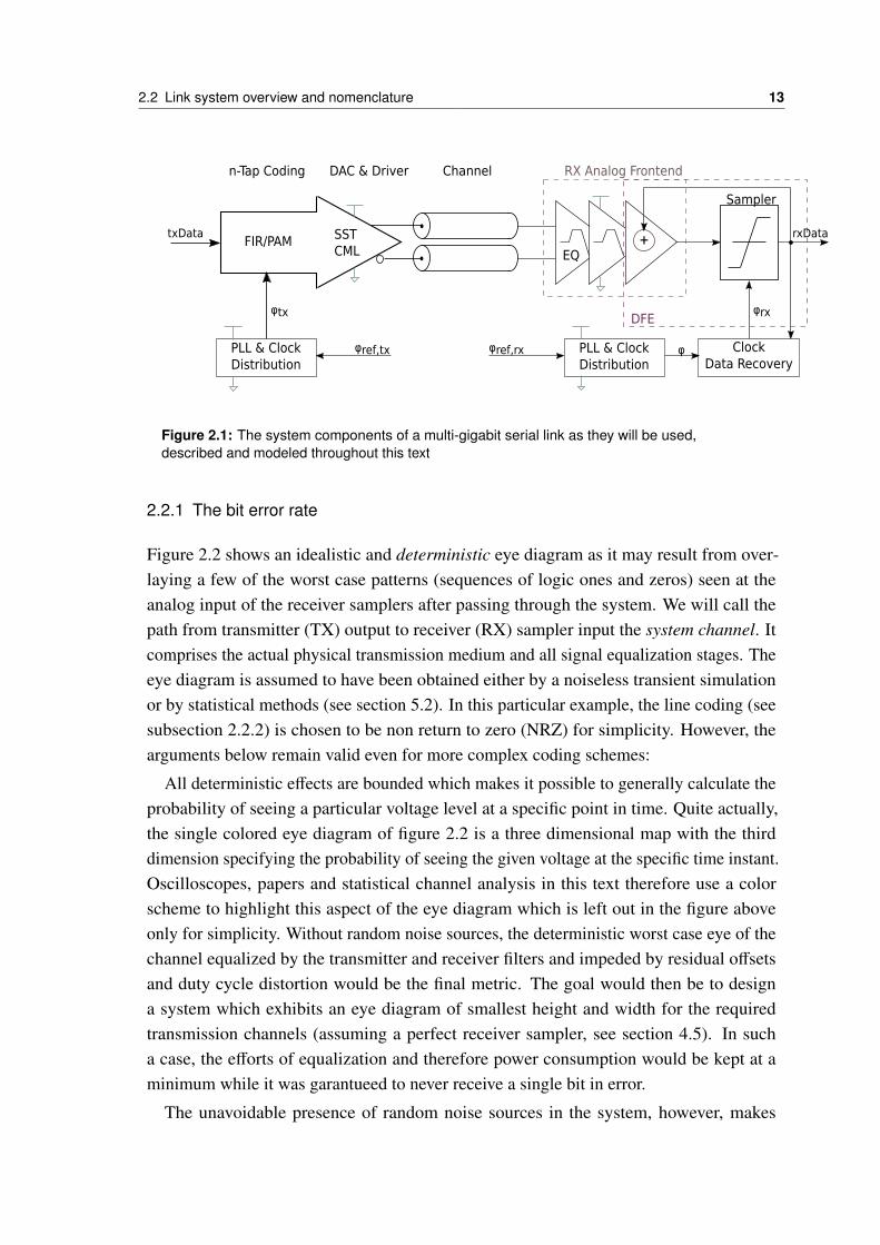
Figure 2.1: The system components of a multi-gigabit serial link as they will be used,described and modeled throughout this text
2.2.1 The bit error rate
Figure 2.2 shows an idealistic and deterministic eye diagram as it may result from over-laying a few of the worst case patterns (sequences of logic ones and zeros) seen at theanalog input of the receiver samplers after passing through the system. We will call thepath from transmitter (TX) output to receiver (RX) sampler input the system channel. Itcomprises the actual physical transmission medium and all signal equalization stages. Theeye diagram is assumed to have been obtained either by a noiseless transient simulationor by statistical methods (see section 5.2). In this particular example, the line coding (seesubsection 2.2.2) is chosen to be non return to zero (NRZ) for simplicity. However, thearguments below remain valid even for more complex coding schemes:
All deterministic effects are bounded which makes it possible to generally calculate theprobability of seeing a particular voltage level at a specific point in time. Quite actually,the single colored eye diagram of figure 2.2 is a three dimensional map with the thirddimension specifying the probability of seeing the given voltage at the specific time instant.Oscilloscopes, papers and statistical channel analysis in this text therefore use a colorscheme to highlight this aspect of the eye diagram which is left out in the figure aboveonly for simplicity. Without random noise sources, the deterministic worst case eye of thechannel equalized by the transmitter and receiver filters and impeded by residual offsetsand duty cycle distortion would be the final metric. The goal would then be to designa system which exhibits an eye diagram of smallest height and width for the requiredtransmission channels (assuming a perfect receiver sampler, see section 4.5). In sucha case, the efforts of equalization and therefore power consumption would be kept at aminimum while it was garantueed to never receive a single bit in error.
The unavoidable presence of random noise sources in the system, however, makes
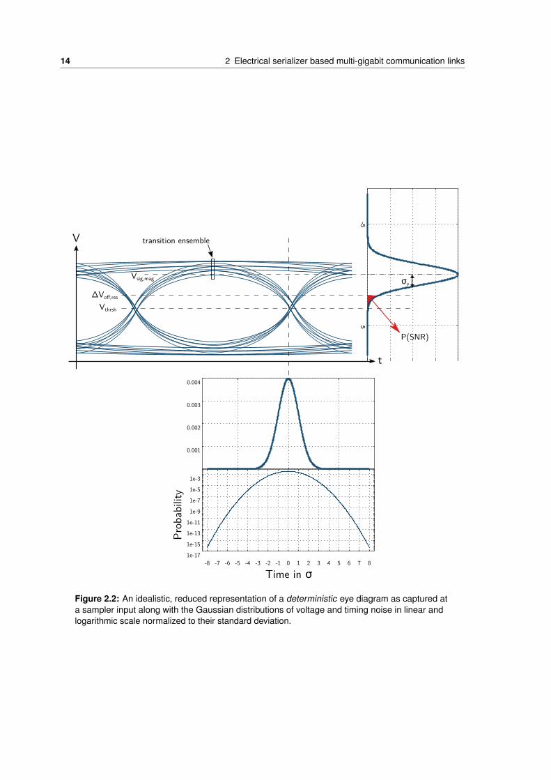
14 2 Electrical serializer based multi-gigabit communication links
1e-171e-151e-131e-111e-91e-71e-51e-3
876543210-1-2-3-4-5-6-7-8
Prob
abilit
y
0.003
0.002
0.001
0.004
5-5
transition ensembleV
t
Time in σ
Vthrsh
ΔVoff,res
Vsig,mag σv
P(SNR)
Figure 2.2: An idealistic, reduced representation of a deterministic eye diagram as captured ata sampler input along with the Gaussian distributions of voltage and timing noise in linear andlogarithmic scale normalized to their standard deviation.
2.2 Link system overview and nomenclature 15
analysis much more complicated. Random noise sources are unbound and in the context ofthis text are all based on underlying physical processes that are wide-sense stationary andergodic. The first restriction ensures consistent process behavior independent of the initialvalue and point in time of the noise source state. The latter garantuees that the process willeventually assume all possible internal states which ensures that by observing the processover time, its PDF can be derived. The combination of all unbound statistical processeswithin the system, such as thermal noise, shot noise or flicker noise (which do themselvesnot adhere to a Gaussian distribution except for thermal noise) will eventually result ina Gaussian distribution of timing and voltage noise due to the central limit theorem ofstatistics. System internal and external noise sources affect the sampler input signal voltageseen at a particular point in time. Depending on the view, this can either be considereda voltage noise or a timing noise (jitter). The slew rate of the signal translates one intothe other and it depends on the subsystem being analyzed which of the views is moreconvenient. The presence and interaction of both types of perturbation to the eye diagramis indicated by the two Gaussian probability density functions in figure 2.2. In addition tothe linear scale of the PDF which is normalized to the standard deviation σ of the process,its logarithmic representation is also shown. It highlights the unbound nature of the processand shows that extreme noise contributions both in voltage and time dimension are possiblealbeit at very low probabilities. For better visibility, a large σ compared to deterministiceye width and height was chosen here.
For a noiseless system, the performance metric is straight forward to define, the eyewidth at the decision threshold (usually chosen to be at 0) and its height for a specificinstant in time can be derived with ease. The system would be said to achieve the giveneye opening at a randomly low error level. With unbound noise sources on the other hand,the eye diagram is closed by definition. It is therefore necessary to define beforehandwhich probability of receiving a bit in error is acceptable - the so called BER. An on-dietransmission system between higher level cache and processor instruction prefetch stagefor instance has only little signal distortion and comparably high transmission levels. It istherefore rather easy to achieve BER levels much lower than 10−30 which makes it unlikelyto even receive a bit in error during the lifetime of the processor itself.
As transmission line properties decrease signal voltage levels to magnitudes comparableto those of the noise sources in the system (thus decreasing the so-called signal to noiseratio (SNR)), more realistic target BERs need to be chosen. In fact, knowing the achievableSNR at the receiver sampler (which is also directly related to the power consumption ofthe transmission system), directly determines the achievable BER level. It is the particularserializer application along with the constraints at higher OSI layers (see section 2.2.2)that call for a specific lower BER bound. For instance a serial link with a transmission rateof 10 Gb/s shall on average only produce a single maldetected bit per minute such thatthe network protocol retransmission procedure does not have a severe impact on total link
16 2 Electrical serializer based multi-gigabit communication links
performance. This is equivalent to a bit error rate of approximately 1.7 · 10−12.
From figure 2.2 it can be seen that it is the integral of the portion of the Gaussian processreaching below the decision threshold which gives the cumulative probability of actuallyreceiving a bit in error. The connection between SNR and BER can therefore be derived to
BER = P(S NR) =1
σV√
2π
S NR·σV∫−∞
e−12
( x−Vsig,magσV
)2
dx = 0.5 erfc(S NR√
2
)(2.7)
The signal to noise ratio in figure 2.2 can pessimistically be given by
S NR =Vsig,mag − Vthrsh + ∆Voff
σV
In the example of the 10 Gb/s link above, an SNR of about 7 would need to be achievedat the sampler. This is pessimistic in the sense that here we assumed convolution of theGaussian distribution with the worst case transition alone. However, this convolution wouldneed to be performed with the ensemble of all transitions passing through the samplingtime instant ts in the figure (highlighted by the black box) which would of course reducethe relative impact of the worst case transition in accordance to its probability of actuallyoccuring in a given bit pattern (see chapter 5 for more information on this process). Notealso, that the probabilites of the Gaussian plots in figure 2.2 are neither scaled with theprobability of the worst case transition nor can the probability of receiving a bit in errordirectly be read from the graphs. This would additionally involve the abovementionedintegration over the ensemble of all noise source magnitudes which could potentially pushthe voltage level below the decision threshold.
While it is straight forward to analyze the eye diagram in terms of voltage noise (andtherefore uncertainty in voltage amplitude, hence voltage error), uncertainty with respectto instants in time (timing errors) need to be defined and treated more carefully:
There are mainly three different descriptions of timing error which are all interrelated.They are the so-called phase jitter, the period jitter and the cycle to cycle jitter. Thelatter two are important when analyzing autonomously oscillating systems or parallel bussystems where a known timing between serveral lanes is important due to common retimingon the receiving side. With serial links as discussed here, each lane is considered a separatesystem. Retiming can and will be delegated to other layers of the communication stacksuch as the medium access layer (see section 2.2.2 ). The serial link transmits symbols inwell defined time intervals called bit period T or sometimes unit interval UI. The existenceof T is an idealized assumption and helps to quantify the time interval error (TIE) whichis due to residual equalization errors, residual offset errors or phase noise of the clocksources driving the gating structures responsible for creating the potential differences onthe transmission line that ultimately represent the information (bits). It is in this sense that

2.2 Link system overview and nomenclature 17
we can define the phase jitter φn = tn − nT where n ∈ N. While nT would be the momentin time where the ideal signal crossing would occur if the information modulated onto thetransmission line were actually changing, tn is the actual point in time observed for thetransition through the reference level. From a known phase noise PSD S φφ(ω) or its dualautocorrelation function, the RMS time interval error (jitter) can be derived to
σ2φ =
4ω2
0
∞∫0
S φφ(ω)dω =2ω2
0
Rφφ(0) (2.8)
where ω0 =2πT .
The SNR is a voltage domain quantity. For jitter, however, the same derivation can bemade with respect to the time domain. This is indicated by the Gaussian distribution belowthe eye diagram. The decision threshold in this case is the (ideal) sampling instant usuallylocated at the center of the eye. The Gaussian tails to be integrated give the probability ofsampling a bit pre- or succeeding the actual bit to be sampled. It is for this reason, thatthere must always be a triplet of information given to describe the performance of theoverall system: the resulting eye width ew
‡, the eye height eh‡ and the BER‡ level at which
the prior two values were obtained. As the processor example above indicates, a BER for aserial tranmission system should always be given with respect to channel attenuation at theNyquist frequency (and hence serializer data rate) and the system testing pattern used (aPRBS sequence for instance) in cases where a non-statistical analysis is made. Oftentimes,even more information like channel reflections are given too, to highlight the importanceand effectiveness of more involved equalization schemes such as the DFE (see section 3.3).
2.2.2 Interaction with higher communication layers
Figure 2.3 depicts the lowest three layers of the open systems interconnection (OSI) modelwhich are called physical layer, data link layer and the network layer respectively anddefine the constraints for the serializer system. The bulk of digital hardware componentswhich need to implement certain aspects of these layers are omitted in figure 2.1. Theseinclude the muxing and demuxing structure to adapt to on-chip data width and rate, thebuffering structures, power down, idle modes as well as offset and equalization calibrationlogic. They are all not shown as they are handled by the well established digital descriptionand implementation work flow which is ammended by the real number modelling frame-work (see section 4.2 of chapter 4 for details). Also, these aspects, albeit integral part ofthe serializer itself, can conceptually be attributed to the higher layers as well. The specifi-cation items listed in the diagram focus on those aspects of the higher two layers whichconversely exhibit an interaction with the serializer performance at the lowest level. The
18 2 Electrical serializer based multi-gigabit communication links
Line coding &Signal levels
NRZ (PAM-2), Duobinary, PAM-4
Impedance 40/80 to 60/120 Ohms
Channel type Single-ended, Differential, Termination,Coupling (AC/DC)
Physical layer
Link (MAC) Layer
Data coding XB/YB, Scrambling, DBI
Link maintenancePresence detection, calibration phase,equalization, data rate negotiation,power down and sleep modes, recovery
Network LayerPacket definitions Test patterns, NOP/Skip, Data/Control
Packet error correction
Error correction CRC, FEC, fault tolerance
Retransmission, Buffering
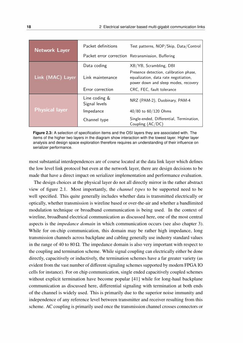
Figure 2.3: A selection of specification items and the OSI layers they are associated with. Theitems of the higher two layers in the diagram show interaction with the lowest layer. Higher layeranalysis and design space exploration therefore requires an understanding of their influence onserializer performance.
most substantial interdependences are of course located at the data link layer which definesthe low level link protocol but even at the network layer, there are design decisions to bemade that have a direct impact on serializer implementation and performance evaluation.
The design choices at the physical layer do not all directly mirror in the rather abstractview of figure 2.1. Most importantly, the channel types to be supported need to bewell specified. This quite generally includes whether data is transmitted electrically oroptically, whether transmission is wireline based or over-the-air and whether a bandlimitedmodulation technique or broadband communication is being used. In the context ofwireline, broadband electrical communication as discussed here, one of the most centralaspects is the impedance domain in which communication occurs (see also chapter 3).While for on-chip communication, this domain may be rather high impedance, longtransmission channels across backplane and cabling generally use industry standard valuesin the range of 40 to 80Ω. The impedance domain is also very important with respect tothe coupling and termination scheme. While signal coupling can electrically either be donedirectly, capacitively or inductively, the termination schemes have a far greater variety (asevident from the vast number of different signaling schemes supported by modern FPGA IOcells for instance). For on chip communication, single ended capacitively coupled schemeswithout explicit termination have become popular [41] while for long-haul backplanecommunication as discussed here, differential signaling with termination at both endsof the channel is widely used. This is primarily due to the superior noise immunity andindependence of any reference level between transmitter and receiver resulting from thisscheme. AC coupling is primarily used once the transmission channel crosses connectors or
2.2 Link system overview and nomenclature 19
even systems (compute nodes for instance) while DC connections are preferred whenevertight control of the entire system to be implemented is possible. An example for this wouldbe a memory module (such as HMC) connected to a CPU on the same board or evenpackage where the power as well as the reference clock distribution are part of the systemsdesign space.
In addition to impedance the line coding and signal levels for data transmission andreception need to be defined. The line coding is specified in the physical layer and one ofthe earliest design decisions of all. In this text, the focus solely lies on NRZ coding. Thisis, for the most part, due to its wide popularity and the interoperability requirements of theserializer whose development was assisted by this work. Another more complex choicefor line coding may have been a duobinary or ternary coding scheme. Essentially, thesecodes exhibit a vastly different power spectral density (see section 3.4) with a redistributionof signal alphabet power in favor of lower frequency. Especially in high loss, long haulchannels, this can substantially facilitate equalization efforts or the feasibility of powerconstraints. A much more involved choice offers a scheme such as a PAM-N code, wherePAM stands for pulse amplitude modulation (PAM). A transceiver which utilizes NRZline coding is also said to be using a PAM-2 scheme. There have been publications onPAM-4 systems [4, 32, 28, 13] which, with the advent of 100G Ethernet finally arrive at acommercial level as well. There is a substantial increase in design complexity associatedwith PAM-4, especially at the receiver (refer to caption of figure 2.12). Not only does thenumber of samplers and clocking resources increase. Also, equalization schemes and clockdata recovery analysis are much more involved. The benefit ultimately lies in the relaxedequalization requirements compared to a PAM-2 system with the same baud rate. Thebaud rate is the number of symbols transmitted per second. An NRZ code encodes a singlebit per bittime with its two voltage levels. A PAM-4 code on the other hand transmits twosymbols per bit time with its four defined voltage levels.
At the link layer, one of the most influential decisions with respect to serializer perfor-mance and constraining is the data coding. Popular coding schemes are XB/YB schemesin which words of data to be transmitted are translated from X to Y bits with Y beinggreater than X. Concepts of how this transformation is carried out differ substantially forthe various choices of X. In the past, one of the most popular choices has been 8B/10Bcoding [64] which used a predefined translation table under omission of some of the 10Bit codes to guarantee a DC balance in the signal over a well defined run length. The DCbalance constraint was meant to avoid a shift of the common mode voltage at the receivingsamplers which would result in a reduction of the effective signal to noise ratio. At thesame time, there is a guaranteed number of transitions per unit time so that AC coupledtransmission lines may be used. Also, the clock recovery mechanisms all rely on trackingsignal transitions and will therefore leave the ideal sampling instant (i.e. loose lock ) whena specific lower bound for the transition density can not be upheld. When designing the
20 2 Electrical serializer based multi-gigabit communication links
clock recovery circuit of a receiver, this is a very central aspect which requires thoroughanalysis. 8B/10B coding with its high transition density is a rather conservative choice inthis regard and comes at a pretty substantial cost: only 80 percent of all bits transmittedactually convey user information. This is why in recent years, other combinations of X andY have become more popular. The two most prominent are 64B/66B (10 Gigabit Ethernet/ Fibre Channel) as well as 128B/130B (PCI-E 3.0). In both cases, there is no explicittransformation table. To ensure a statistical DC balance, the transmitter scrambles the datawith a linear feedback shift register of a predefined polynomial while the receiving sideinverts this process to recapture the original data. Theoretically, it is possible to force ascrambler into producing an indefinitely long sequence of static bits with a well chosensuccession of input data. Usually, user data exhibits a good level of variability which thescrambling in turn will convert to a well randomized output bit stream (and therefore toa spectrally white frequency distribution). This may also be important for equalizationtraining algorithms, especially the widely popular SS-LMS algorithm (see section 3.3)which rely on an equal symbol probability distribution.
Link initialization and management are also vital aspects of the link layer. In thiscontext, the procedures in which a link is powered up or down, calibrated (to compensatecircuit mismatches) or even set up with respect to its data rate and equalization need tobe defined. If automatic adaption schemes are to be implemented in hardware, one of thekey aspects to investigate is how to perform digital loop based equalization proceduresand how these calibration loops respond to an elevated, initial bit error level. Anotherimportant aspect in this context is the definition of link operability. Usually, a link is saidto be operable once it reaches the predefined bit error rate (see next subsection). Thebit error rate cannot achieve low levels of statistical insignificance in all transmissiondomains, especially not within the domain primarily described in this text. The link layertherefore also needs to implement an error detection and recovery mechanism if the overallcommunication stack specification aims to avoid severe latency penalties as would beincurred if retransmissions of faulty data were delegated to higher OSI layers. Errordetection and correction schemes can for instance be realized by forward error correction(FEC) or by cyclic redundancy checks (CRC). Fault recovery when failing to correct thereceived data may include the retransmission of the faulty packet. A thorough analysisof which error levels still allow to maintain an operable link within given performancespecifications may allow to tweak overall power consumption and aid in the developmentof robust link transmission protocols. This again requires a serializer model which isclosely tied to its physical implementation but simulates magnitudes faster.
The network layer may also benefit from a concise transceiver model. When definingtest patterns and the overall package structure of the network, a thorough analysis mayhelp to increase the overall power efficiency of the system and may expose new ways ofimplementing network power states and utilization awareness. This in turn helps to avoid
2.2 Link system overview and nomenclature 21
overconstraining the metrics for the serializer itself.
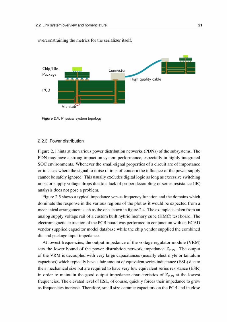
Chip/DiePackage
PCB
Connector
High quality cable
Via stub
Figure 2.4: Physical system topology
2.2.3 Power distribution
Figure 2.1 hints at the various power distribution networks (PDNs) of the subsystems. ThePDN may have a strong impact on system performance, especially in highly integratedSOC environments. Whenever the small-signal properties of a circuit are of importanceor in cases where the signal to noise ratio is of concern the influence of the power supplycannot be safely ignored. This usually excludes digital logic as long as excessive switchingnoise or supply voltage drops due to a lack of proper decoupling or series resistance (IR)analysis does not pose a problem.
Figure 2.5 shows a typical impedance versus frequency function and the domains whichdominate the response in the various regions of the plot as it would be expected from amechanical arrangement such as the one shown in figure 2.4. The example is taken from ananalog supply voltage rail of a custom built hybrid memory cube (HMC) test board. Theelectromagnetic extraction of the PCB board was performed in conjunction with an ECADvendor supplied capacitor model database while the chip vendor supplied the combineddie and package input impedance.
At lowest frequencies, the output impedance of the voltage regulator module (VRM)sets the lower bound of the power distrubtion network impedance ZPDN. The outputof the VRM is decoupled with very large capacitances (usually electrolyte or tantalumcapacitors) which typically have a fair amount of equivalent series inductance (ESL) due totheir mechanical size but are required to have very low equivalent series resistance (ESR)in order to maintain the good output impedance characteristics of ZPDN at the lowestfrequencies. The elevated level of ESL, of course, quickly forces their impedance to growas frequencies increase. Therefore, small size ceramic capacitors on the PCB and in close
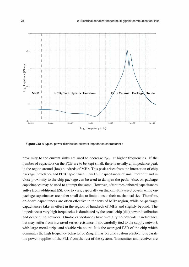
22 2 Electrical serializer based multi-gigabit communication links
Log. Frequency (Hz)
0
-0.5
-1
-1.5
-2
-2.51e+091e+081e+071e+061e+051e+041e+03
Log.
Impe
danc
e (O
hms)
VRM PCB/Electrolyte or Tantalum PCB Ceramic Package On die
Figure 2.5: A typical power distribution network impedance characteristic
proximity to the current sinks are used to decrease ZPDN at higher frequencies. If thenumber of capacitors on the PCB are to be kept small, there is usually an impedance peakin the region around (low) hundreds of MHz. This peak arises from the interaction of chippackage inductance and PCB capacitance. Low ESL capacitances of small footprint and inclose proximity to the chip package can be used to dampen the peak. Also, on-packagecapacitances may be used to attempt the same. However, oftentimes onboard capacitancessuffer from additional ESL due to vias, especially on thick multilayered boards while on-package capacitances are rather small due to limitations to their mechanical size. Therefore,on-board capacitances are often effective in the tens of MHz region, while on-packagecapacitances take an effect in the region of hundreds of MHz and slightly beyond. Theimpedance at very high frequencies is dominated by the actual chip (die) power distributionand decoupling network. On-die capacitances have virtually no equivalent inductancebut may suffer from increased series resistance if not carefully tied to the supply networkwith large metal strips and sizable via count. It is the averaged ESR of the chip whichdominates the high frequency behavior of ZPDN. It has become custom practice to separatethe power supplies of the PLL from the rest of the system. Transmitter and receiver are
2.2 Link system overview and nomenclature 23
usually tied together in a common domain. In order to minimize interactions betweenthe digital, complementary metal oxide semiconductor (CMOS) and therefore switchingnoise dominated part and the analog, often current mode logic (CML) dominated and noisesensitive part of the design, a separation of digital and analog supplies on the level of chipand package has also been used. Additionally, with a shrink in technology feature sizes,the core voltage decreases, too, due to smaller gate oxide thicknesses. While 65 nm nodescan still be operated with up to 1.2 Volts, the 22 nm node forces designers to work withsupplies as low as 0.7 Volts. This quickly becomes a problem for all I/O standards andspecifically to serializers (see also subsection 2.2.5). The alternative of using thick-oxidetransistors when designing for smaller technology nodes neccessitates a further supply andPDN which leads to design challenges especially on the packaging level but may havea favourable impact on the supply noise characteristics in conjuction with other specificdesign choices (see again subsection 2.2.5). As can be seen from this discussion, there is alot of information required to obtain a meaningful ZPDN. In addition to the vendor suppliedcharacteristics of capacitors and VRM, at least a 2.5D field solver based extraction of thepower distribtion network (PCB and package) is required. Also, a good estimate of thetotal die capacitance and ESR is needed as well. Typically this kind of information is onlyavailable very late in the design phase. Therefore, it is common practice to model the PDNas a bandwidth limited thermal noise source with a power spectral density of either
S VV, LP(ω) =
√π(1 +
√2)σ2
vn,pdn
ω3db,pdn·
1
1 +(ω
ω3db,pdn
)2 (2.9)
or (much more unphysical and even discontinuous)
S VV, Box(ω) =
σ2
vn,pdn
ω3db,pdn, 0 ≤ ω < ω3db,pdn
0 , else
where in both cases σvn,pdn‡ is the actual in-band RMS voltage noise and ω3db,pdn
‡ thePDN bandwidth. The additional factor for the lowpass filter type is chosen such that inboth cases we obtain
ω3db,pdn∫0
S VV(ω)dω = σ2pdn
and thereby ensure that the noise power contribution made by the PDN to the system is welldefined by the parameter σvn,pdn. Note that here, we drop the notion of the PDN having animpedance alltogether and think of it plainly as a source of noise power. This noise powerwould normally originate from the interaction of the systems current consumption S I(ω)
24 2 Electrical serializer based multi-gigabit communication links
(given in its spectral form) with the PDN impedance which is also a complex quantitiy.The voltage spectral density seen at the power supply would then be given by
S V(ω) = S I(ω) · ZPDN(ω)
and its equivalent voltage noise can be determined from the resulting PSD as S VV(ω) =|S V(ω)|2. As mentioned above, a good estimate of both SI(ω)‡ and ZPDN(ω)‡ can generallybe obtained with substantial effort and can potentially be included in budgeting procedures.Conversely, it is possible to use budgeting approaches to produce meaningful constraints toZPDN(ω) as board and package implementation design input. Care must be taken, however,to not delegate too much of the noise reduction efforts to system designers as their designspace is much more limited compared to the IC design itself. The equivalent noisesource approach of course assumes that the noise seen at the power supply is completelyuncorrelated with serializer events. Evidently, this is especially untrue for CMOS typelogic of which an increasing amount will be found in the serializers of the nodes andyears to come. While for the initial system design phase, the simple model serves itspurpose, the final design verification and sign-off should rely on more elaborate methods.An intermediate solution to the problem is the definition of an impedance mask and thededuction of approximate time resolved current consumption as part of the modelingprocess.
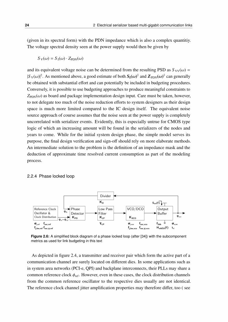
2.2.4 Phase locked loop
Reference ClockOscillator & Clock Distribution
φin=φref
σj,ref
SVV(f)
Phase Detector
Low PassFilter
VCO/DCO OutputBuffer
Divider
φout
φfb
KPD
τLP
KXCOKLP
fosc,reffj,bw,ref fosc,γ,ref
σj,xco fosc,xcofj,bw,xco fosc,γ,xco
KD
f3dbHvdd2o(f)
σn,int
trf
Figure 2.6: A simplified block diagram of a phase locked loop (after [34]) with the subcomponentmetrics as used for link budgeting in this text
As depicted in figure 2.4, a transmitter and receiver pair which form the active part of acommunication channel are surely located on different dies. In some applications such asin system area networks (PCI-e, QPI) and backplane interconnects, their PLLs may share acommon reference clock φref . However, even in these cases, the clock distribution channelsfrom the common reference oscillator to the respective dies usually are not identical.The reference clock channel jitter amplification properties may therefore differ, too ( see
2.2 Link system overview and nomenclature 25
section 5.3.4) which may in turn lead to differing characteristics for the two PLLs. In HPCnetworking applications, the reference oscillators are certainly not identical whereas theclock distribution channel usually is (if a reference oscillator is located on the networkinterface controller (NIC) PCB). In this case, a single PLL model for both sides is sufficient.The reference oscillator together with its clock distribution channel is not shown in figure2.1 as it is a part of the phase locked loop (PLL) model here. The task of a PLL is togenerate a high frequency, low jitter reference clock for the transmitter and receiver clockdividers, its (de-)mux stages, the transmitter output driver and the receiver samplers. It isdistributed to transmitter and receiver via the on-chip clock tree. The effect of on-die clockdistribution is logically assigned to transmitter and receiver domains and will be discussedbelow. The effect of clock distribution from the high precision reference oscillator (usuallya quartz with an oscillation frequency of a few MHz) can potentially be integrated withits model representation directly. Figure 2.6 shows a typical PLL block diagram togetherwith the metric symbols used for budgeting. The design space of these subcomponents isquite large and well beyond the scope of this text. Fortunately, irrespective of the exactimplementation, it is usually possible to model a PLL as a second order transfer functionin phase space. Ultimately, for the system presented here, the relevant high level metric ofthe PLL is the phase noise power spectral density Sφφ(ω)‡ including the effects of the PLLpower supply. If it is known beforehand and the PLL is no part of the design budgetingprocess, it is the single piece of information required for deriving constraints for othersubcomponents. If the PLL design effort shall be part of the constraining efforts, however,a good or at least rough approximate shape of the phase noise PSD is of importance. Itis the spectral content of this jitter that will impede the transmitter output, be potentiallyamplified by the channel and be finally processed by the clock data recovery circuit ofthe receiver. Therefore, it will have a significant impact on the system performance (seesection 2.2.6). In a final implementation S φφ(ω) will be obtained by a periodic steady stateand periodic noise simulation as offered by modern RF Spice simulators. The sensitivityof the PLL to noise on the power supply can also be obtained in this way - the necessaryanalysis is called the periodic transfer function (PXF) simulation and is also beyond thescope of this text. As is the case with detailed PDN metrics, these simulations can only beobtained fairly late in the design phase. For design space analysis and budgeting purposes,the condensed second order model as suggested by Mansuri and Kang [34] and as alsoused by the PCI Express Jitter modelling specification [47] will be used: The prototypicalsecond order phase transfer function of a PLL in phase space is given as [34]
HPLL(s) =φout
φin=
2ζωns + ω2n
s2 + 2ζωns + ω2n
(2.10)
where ωn is the PLL natural frequency and ζ the damping factor of the closed loop system.The relation between natural frequency and the 3 dB cutoff frequency of the PLL equates
26 2 Electrical serializer based multi-gigabit communication links
to ω3dB = ωn
√1 + 2ζ2 +
√(1 + 2ζ2)2 + 1. On the one hand, we do not particularly care
about the exact interdependences of a detailed PLL design here. On the other hand, wewould like to use the link budgeting procedure and framework to derive general targetspecification values for the subcomponents of the PLL and weigh their impact against othersubdesign choices. Therefore, we will go a step further than the two bare performanceparameters mentioned above and discuss the PLL design in some more detail (see againfigure 2.6). This is also necessary to arrive at the ultimate goal of obtaining a phase noisePSD for the PLL output - the various noise sources and their contribution to the noise seenat the output need to be taken into account in this case.
Frequency (Hz)
0
-50
-100
-150
-2001e+71e+61e+51e+41e+31e+2
Lorentzian
1/f^2 with lower bound
Simple 1/f^2
Pha
se n
ois
e P
SD
(1/
Hz)
Frequency (Hz)
2.5e-011
2e-011
1.5e-011
1e-011
5e-012
01e+71e+61e+51e+4
Simple 1/f^2
1/f^2 with lower bound
Lorentzian
1e+31e+2
Pha
se n
ois
e P
SD
(db
C/H
z)
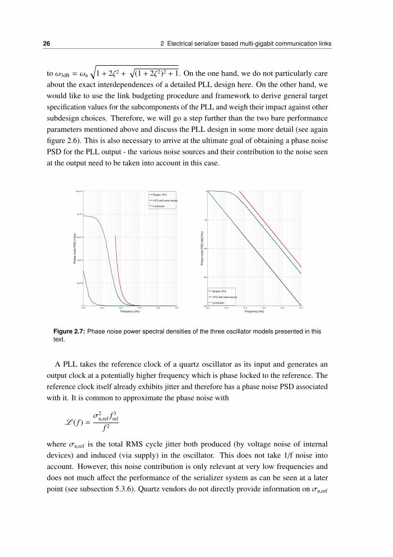
Figure 2.7: Phase noise power spectral densities of the three oscillator models presented in thistext.
A PLL takes the reference clock of a quartz oscillator as its input and generates anoutput clock at a potentially higher frequency which is phase locked to the reference. Thereference clock itself already exhibits jitter and therefore has a phase noise PSD associatedwith it. It is common to approximate the phase noise with
L ( f ) =σ2
n,ref f 3ref
f 2
where σn,ref is the total RMS cycle jitter both produced (by voltage noise of internaldevices) and induced (via supply) in the oscillator. This does not take 1/f noise intoaccount. However, this noise contribution is only relevant at very low frequencies anddoes not much affect the performance of the serializer system as can be seen at a laterpoint (see subsection 5.3.6). Quartz vendors do not directly provide information on σn,ref
2.2 Link system overview and nomenclature 27
in their datasheets. Fortunately, this is not necessary as the usual information on the totalRMS output jitter of the quartz σj,ref
‡ along with its center frequency of oscillation fref‡
are enough for the most simple model. Due to equation 2.8 the following relation for thegiven parameters hold:
σj,ref =4
(2π fref)2
fj,BW∫1
2L ( f )d f → σn,ref =πσj,ref√
2 fref
Along with the total output jitter, vendors usually supply the frequency bandwidth fj,BW‡
across which the measurement was made. For the simple 1/ f 2 model given here, thisinformation, albeit used during the integration of the phase noise PSD, does not affectthe model value σn,ref. This is due to the divergent nature of the phase noise function forf → 0 which is also the reason for restricting the integration above towards the lowerbound to 1 Hz. This restriction of the integration interval essentially states that the bulk ofnoise power as given by σn,ref concentrates within 2 Hz around the carrier. This frequencyprecision cannot even be achieved with the best devices on the market. Some spectralbroadening around the central carrier frequency can always be observed. If this broadeningis described with the parameter fosc,γ
‡ the integration above gives
σn,ref =πσj,ref√
2 fref
(fj,BW fosc,γ
fj,BW − fosc,γ
)The rather unrealistic notion that frequencies below fosc,γ do not contribute to overall phasenoise power puts more energy into higher frequency bands. This overestimation, however,may lead to more conservative overall designs. The error made by approximating thereference oscillator phase noise by almost Dirac like functions can be resolved by usinga Lorentzian model. It has been shown that oscillators, much like many other resonatingphysical systems, exhibit a spectral phase noise power distribution that adheres to thisform[49]:
L ( f ) =c f 2
oscσ2n,ref
(π f 2osc c)2 + f 2 where c =
fosc,γ
2π f 2osc
Here, for a given RMS output jitter collected over a defined frequency band, it can beshown that the parameter σn,ref can be derived from the model parameters according to
σn,ref = πσj,ref fosc
√π
2atan( fj,BW
π f 2oscc
)Figure 2.7 compares the three presented models. The left picture displays phase noisemagnitude and shows how the Lorentzian spectrum takes a position in between the two
28 2 Electrical serializer based multi-gigabit communication links
simplistic models. The right hand side compares the functions on basis of the morecommon logarithmic representation of phase noise normalized to the respective power atthe "central frequency of oscillation" (in dbC
Hz ). Here, it becomes apparent that the simple1/ f 2 model will produce a much too optimistic noise level due to the unrealistic spectralbroadening of a few Hertz. On the other hand, the lower bound limited derivation of thismodel can potentially be used as a conservative estimate, especially given the fact thatinformation about the spectral width of the central oscillation may not always be available.The phase noise of the reference oscillator undergoes a coloring process in the PLL thatis given by the PLL transfer function 2.10. Its contribution to the total PLL phase noisePSD can thus be computed straight forward provided that values for natural frequencyand damping factor are known. After all, this is exactly what the PLL is supposed to do:track all low frequency variations within a given bandwidth and reject the remainder whichusually originates from unwanted perturbations such as electromagnetic interference orclock distribution related noise.
The natural frequency depends on the so-called open loop gain Kloop which in turndepends on the phase detector gain KPD
‡, the lowpass filter decimation gain KLP‡, the
gain of the voltage controlled oscillator KXCO‡ and the divider feedback gain KD
‡ suchthat ωn =
√Kloop =
√KPDKLPKDKXCO. The damping factor ζ on the other hand can be
shown to adhere to ζ = ωnτLP2 where τLP
‡ is the lowpass filter time constant. All of thesesubcomponent parameters separate the PLL design into manageable portions and theirso-defined metrics. They, of course, strongly depend on the particular, underlying designof the PLL subcomponents but can generally be derived in simulations.
The phase detector compares a divided version of the PLL output clock with the referenceand produces a signal at its output that is proportional to the phase difference of the two.It, too, could either be implemented with a linear or a digital (bang-bang) approach.The resulting phase detector gain Kpd is more involved to analyze for the latter (as alsomentioned in subsection 2.2.6 in the context of the receivers clock data recovery). Thelowpass filter reduces the variability in the sequence of phase detector information anduses it to drive the voltage or digital controlled oscillator (XCO) which in turn needsto produce an input signal proportional frequency at its output. The phase detector, thedivider and the lowpass filter are thought of as noiseless components. This is becauseeither they may be built from passive devices with a narrow frequency band (low pass) andwith their 1/f contribution ignored (which makes their overall noise contribution at verylow frequencies negligible). The other reason may be that they are realized using all digitalcomponents (phase detector, divider and in all digital PLLs even the low pass). As a matterof fact, in recent years all digital phase locked loops (ADPLL) have become increasinglypopular as their properties are affected favorably by technology shrinks compared to theirall analog counterparts. For a more detailed treatment, refer to [38]. Therefore, the tworemaining subdesigns with contribution to PLL output phase noise here are the XCO and
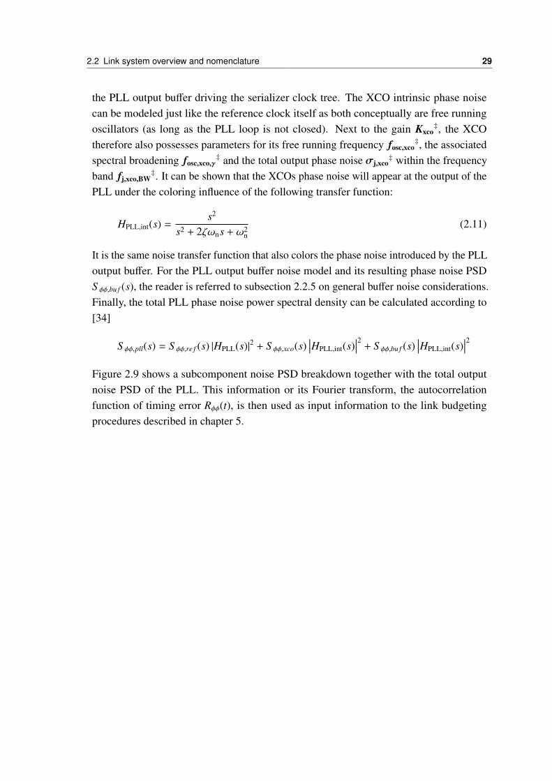
2.2 Link system overview and nomenclature 29
the PLL output buffer driving the serializer clock tree. The XCO intrinsic phase noisecan be modeled just like the reference clock itself as both conceptually are free runningoscillators (as long as the PLL loop is not closed). Next to the gain Kxco
‡, the XCOtherefore also possesses parameters for its free running frequency fosc,xco
‡, the associatedspectral broadening fosc,xco,γ
‡ and the total output phase noise σj,xco‡ within the frequency
band fj,xco,BW‡. It can be shown that the XCOs phase noise will appear at the output of the
PLL under the coloring influence of the following transfer function:
HPLL,int(s) =s2
s2 + 2ζωns + ω2n
(2.11)
It is the same noise transfer function that also colors the phase noise introduced by the PLLoutput buffer. For the PLL output buffer noise model and its resulting phase noise PSDS φφ,bu f (s), the reader is referred to subsection 2.2.5 on general buffer noise considerations.Finally, the total PLL phase noise power spectral density can be calculated according to[34]
S φφ,pll(s) = S φφ,re f (s) |HPLL(s)|2 + S φφ,xco(s)∣∣∣HPLL,int(s)
∣∣∣2 + S φφ,bu f (s)∣∣∣HPLL,int(s)
∣∣∣2Figure 2.9 shows a subcomponent noise PSD breakdown together with the total outputnoise PSD of the PLL. This information or its Fourier transform, the autocorrelationfunction of timing error Rφφ(t), is then used as input information to the link budgetingprocedures described in chapter 5.
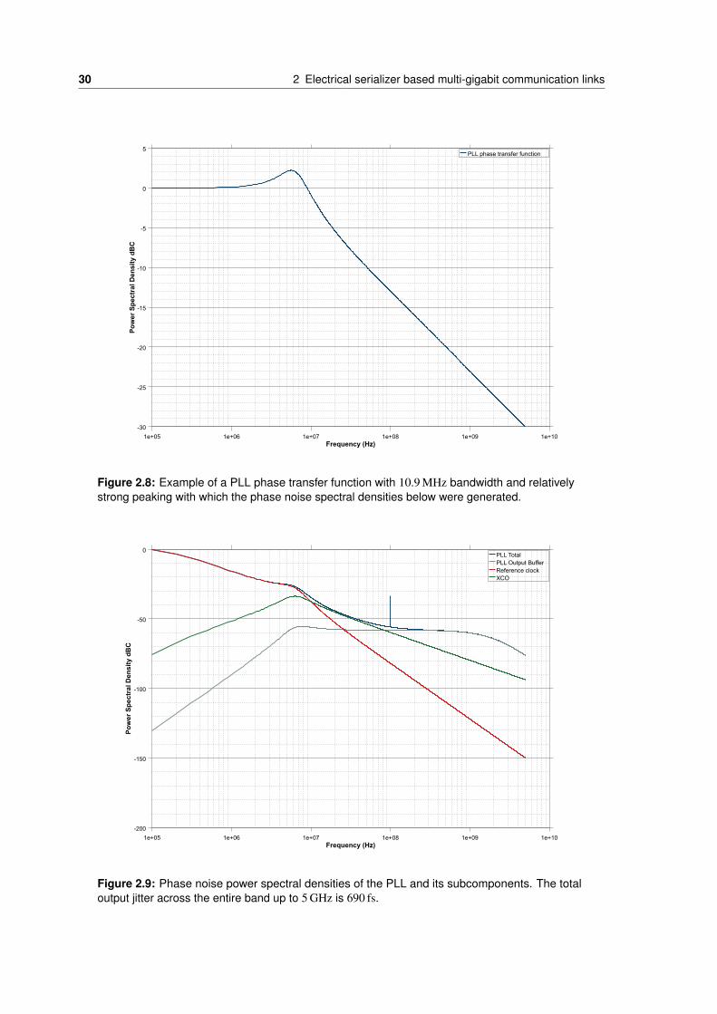
30 2 Electrical serializer based multi-gigabit communication links
1e+05 1e+06 1e+07 1e+08 1e+09 1e+10
-30
-25
-20
-15
-10
-5
0
5
Frequency (Hz)
Po
wer
Sp
ectr
al D
ensi
ty d
BC
PLL phase transfer function
Figure 2.8: Example of a PLL phase transfer function with 10.9 MHz bandwidth and relativelystrong peaking with which the phase noise spectral densities below were generated.
1e+05 1e+06 1e+07 1e+08 1e+09 1e+10
-200
-150
-100
-50
0
Frequency (Hz)
Po
wer
Sp
ectr
al D
ensi
ty d
BC
PLL TotalPLL Output BufferReference clockXCO
Figure 2.9: Phase noise power spectral densities of the PLL and its subcomponents. The totaloutput jitter across the entire band up to 5 GHz is 690 fs.
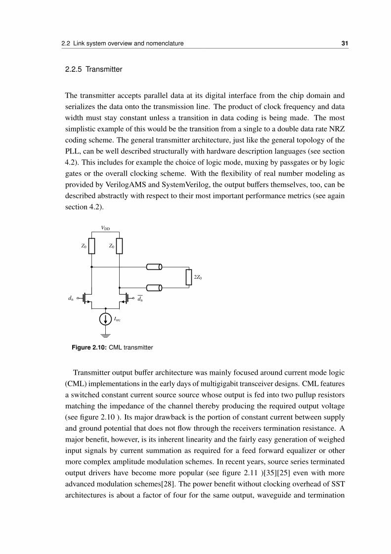
2.2 Link system overview and nomenclature 31
2.2.5 Transmitter
The transmitter accepts parallel data at its digital interface from the chip domain andserializes the data onto the transmission line. The product of clock frequency and datawidth must stay constant unless a transition in data coding is being made. The mostsimplistic example of this would be the transition from a single to a double data rate NRZcoding scheme. The general transmitter architecture, just like the general topology of thePLL, can be well described structurally with hardware description languages (see section4.2). This includes for example the choice of logic mode, muxing by passgates or by logicgates or the overall clocking scheme. With the flexibility of real number modeling asprovided by VerilogAMS and SystemVerilog, the output buffers themselves, too, can bedescribed abstractly with respect to their most important performance metrics (see againsection 4.2).
dn dn
Isrc
Z0 Z0
VDD
2Z0
Figure 2.10: CML transmitter
Transmitter output buffer architecture was mainly focused around current mode logic(CML) implementations in the early days of multigigabit transceiver designs. CML featuresa switched constant current source source whose output is fed into two pullup resistorsmatching the impedance of the channel thereby producing the required output voltage(see figure 2.10 ). Its major drawback is the portion of constant current between supplyand ground potential that does not flow through the receivers termination resistance. Amajor benefit, however, is its inherent linearity and the fairly easy generation of weighedinput signals by current summation as required for a feed forward equalizer or othermore complex amplitude modulation schemes. In recent years, source series terminatedoutput drivers have become more popular (see figure 2.11 )[35][25] even with moreadvanced modulation schemes[28]. The power benefit without clocking overhead of SSTarchitectures is about a factor of four for the same output, waveguide and termination

32 2 Electrical serializer based multi-gigabit communication links
VDD
dn
≈ Z0
VDD
dn
≈ Z0
2Z0
Figure 2.11: SST transmitter
impedance. A further power benefit can be achieved, if transmitter and receiver alikeare designed to operate single-ended instead of differentially[50]. These setups, however,require good control of current return paths across the power planes and are less noiseimmune which makes them appropriate mainly for short-haul applications.
The design tradeoff between CML and SST is an increase in overall complexity andmore stringent requirements on duty cycle distortion control, output impedance adjustmentcircuitry and linearity analysis. Also, due to the reduction of supply voltage in moreadvanced technology nodes, it becomes ever more difficult to realize the output amplitudesrequired to support more sophisticated modulation schemes. Remedies to this circumstancehave been conceived in the past ranging from thick oxide output stages to stacked andcapacitively coupled thin oxide drivers [35]. CML output stages, on the other hand, sufferfrom severe clock feedthrough in advanced technology nodes when combining output stageand last multiplexer stage. This stems from the increasing size of the gate drain capacitancewith respect to the gate source capacitance of the transistors in these technology nodes.The details are again beyond the scope of the discussion here.
For a more general analysis, the transmitter architecture is thought of being a voltagemode digital to analog converter with a preceding weighing matrix such that the inputsymbol stream is buffered and converted to a digital representation of the modulationstrength required at any given point in time. Relevant metrics for its characterization arethe output impedance (tuning range) ZTX
‡, the total output signal swing Vtx,pp‡ and the
output signal rise and fall times tr,tx‡ and tf,tx
‡ (especially their asymmetry which willresult in output common mode variations). The termination and electrostatic dischargeprotection (ESD) compensation quality could also be included as a part of the channel butis attributed to the transmitter here.
As previously discussed, the combination of output rise and fall times, power supplyrejection ratio, power supply noise and internal noise sources will jointly result in the signal
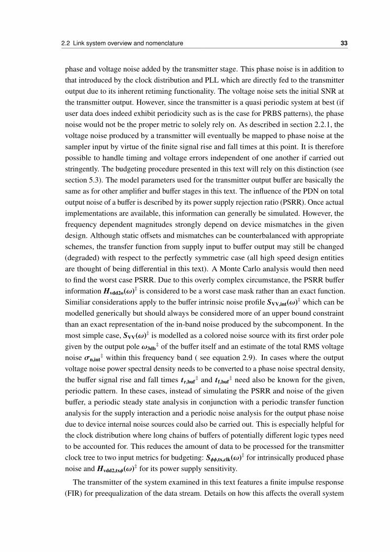
2.2 Link system overview and nomenclature 33
phase and voltage noise added by the transmitter stage. This phase noise is in addition tothat introduced by the clock distribution and PLL which are directly fed to the transmitteroutput due to its inherent retiming functionality. The voltage noise sets the initial SNR atthe transmitter output. However, since the transmitter is a quasi periodic system at best (ifuser data does indeed exhibit periodicity such as is the case for PRBS patterns), the phasenoise would not be the proper metric to solely rely on. As described in section 2.2.1, thevoltage noise produced by a transmitter will eventually be mapped to phase noise at thesampler input by virtue of the finite signal rise and fall times at this point. It is thereforepossible to handle timing and voltage errors independent of one another if carried outstringently. The budgeting procedure presented in this text will rely on this distinction (seesection 5.3). The model parameters used for the transmitter output buffer are basically thesame as for other amplifier and buffer stages in this text. The influence of the PDN on totaloutput noise of a buffer is described by its power supply rejection ratio (PSRR). Once actualimplementations are available, this information can generally be simulated. However, thefrequency dependent magnitudes strongly depend on device mismatches in the givendesign. Although static offsets and mismatches can be counterbalanced with appropriateschemes, the transfer function from supply input to buffer output may still be changed(degraded) with respect to the perfectly symmetric case (all high speed design entitiesare thought of being differential in this text). A Monte Carlo analysis would then needto find the worst case PSRR. Due to this overly complex circumstance, the PSRR bufferinformation Hvdd2o(ω)‡ is considered to be a worst case mask rather than an exact function.Similiar considerations apply to the buffer intrinsic noise profile SVV,int(ω)‡ which can bemodelled generically but should always be considered more of an upper bound constraintthan an exact representation of the in-band noise produced by the subcomponent. In themost simple case, SVV(ω)‡ is modelled as a colored noise source with its first order polegiven by the output pole ω3db
‡ of the buffer itself and an estimate of the total RMS voltagenoise σn,int
‡ within this frequency band ( see equation 2.9). In cases where the outputvoltage noise power spectral density needs to be converted to a phase noise spectral density,the buffer signal rise and fall times tr,buf
‡ and tf,buf‡ need also be known for the given,
periodic pattern. In these cases, instead of simulating the PSRR and noise of the givenbuffer, a periodic steady state analysis in conjunction with a periodic transfer functionanalysis for the supply interaction and a periodic noise analysis for the output phase noisedue to device internal noise sources could also be carried out. This is especially helpful forthe clock distribution where long chains of buffers of potentially different logic types needto be accounted for. This reduces the amount of data to be processed for the transmitterclock tree to two input metrics for budgeting: Sφφ,tx,clk(ω)‡ for intrinsically produced phasenoise and Hvdd2,txφ(ω)‡ for its power supply sensitivity.
The transmitter of the system examined in this text features a finite impulse response(FIR) for preequalization of the data stream. Details on how this affects the overall system

34 2 Electrical serializer based multi-gigabit communication links
response and further implications are presented in the next section.
2.2.6 Receiver
Figure 2.1 also shows the most budgeting relevant subcomponents of the receiver. Aswas the case with the transmitter, this does not include the receiver termination and ESDcompensation, the all digital deserialization stage or the (very complex) clocking scheme.A more detailed picture of transmitter and receiver can be found in chapter 6. For budgetinganalysis, however, the clocking scheme again boils down to the two metrics Sφφ,rx,clk(ω)‡
and Hvdd2,rxφ(ω)‡. While the transmitter did not act on this information at all, the receivermust process its spectral content in a much more complex way. The reason for this liesin the clock data recovery (CDR) circuitry that is used to extract the very clock from thedata stream with which it was put on the transmission line (see below). This is also thereason for the increase in clock distribution complexity. There must be a subcomponentin place that allows to phase shift the receivers sampling clock at a level of reasonablegranularity. In the past, all analog solutions based on voltage controlled oscillators (VCO)have been used for this purpose and it is no coincidence that analysis and metrics of clockdata recovery resemble that of PLLs somewhat - a circumstance this text aims to exploitfor budgeting at a later point (see section 5.3). As PLL designs transition to more digitalimplementations for future technology nodes, CDR designs follow suit. The role of theVCO as a voltage to frequency/phase translation unit is replaced by a digital to phaseconverter with the phase interpolator being the most popular implementation ( see below). Before clock recovery can be attempted, however, the incoming data signal needs tobe preprocessed. In broadband communication systems, the major equalization effort isusually performed in the receiving side. This includes the time continous equalizationstages (CTLE), oftentimes variable gain amplifiers (VGA) and, especially in the contextof backplane channels, decision feedback equalization (DFE). For more information onequalization and its effect on overall system response, the reader is again referred to thenext chapter.
One of the most central subcomponents of the receiver is the sampler (actually the bankof samplers). Here, the analog, equalized but noise impaired input signal is converted backto a digital representation. Depending on the line coding scheme, the number of availableclock phases and the CDR phase detector design (see below), the receiver architecture mayrequire a substantial amount of samplers. For a detailed discussion on the sampler modelused in this text, refer to section 4.5. The overall architecture of the receiver can againbe described very well with a structural, hardware description language based approach.Deterministic effects of the architecture such as residual offsets after calibration, duty cycledistortion, the comparably large time constants of the CDR (see below) or the effects ofresidual intersymbol interference (see next section) can thus be analyzed and accounted
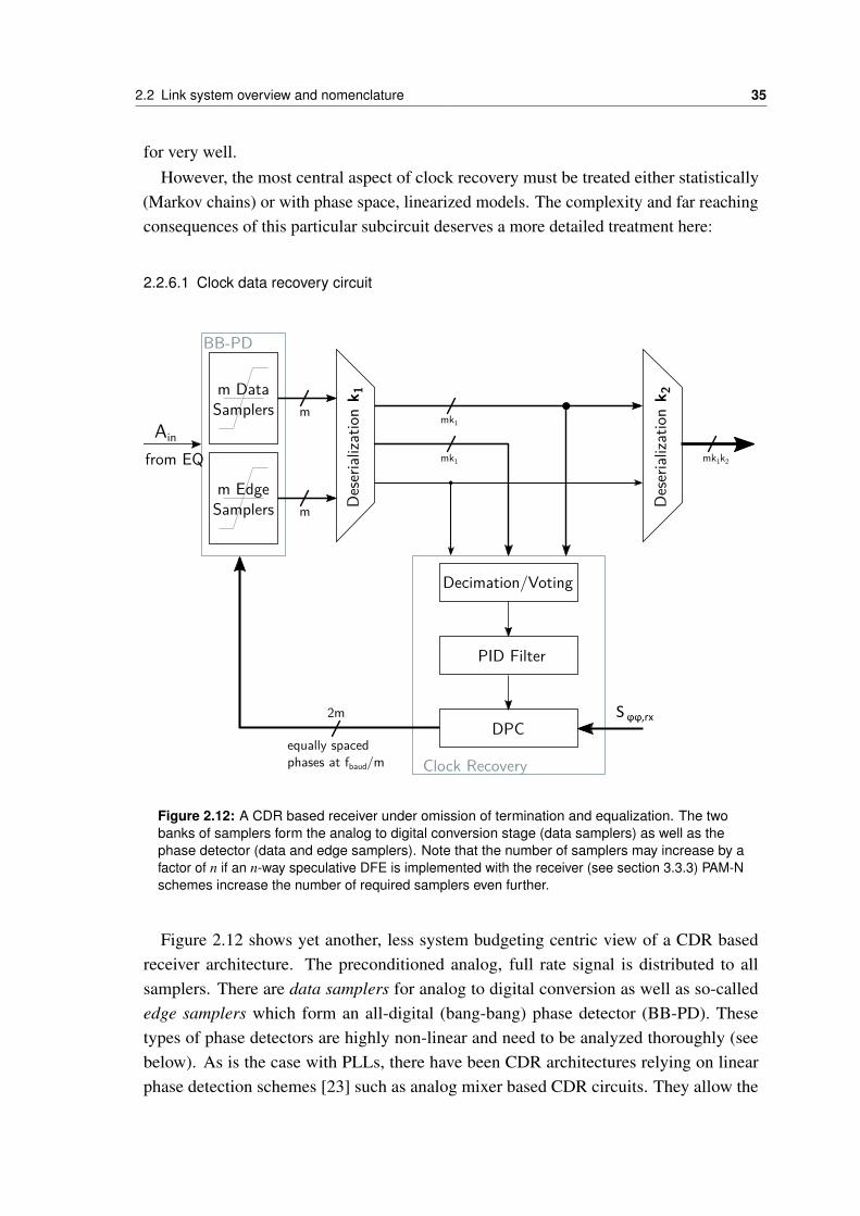
2.2 Link system overview and nomenclature 35
for very well.However, the most central aspect of clock recovery must be treated either statistically
(Markov chains) or with phase space, linearized models. The complexity and far reachingconsequences of this particular subcircuit deserves a more detailed treatment here:
2.2.6.1 Clock data recovery circuit
BB-PD
m DataSamplers
m EdgeSamplers
Decimation/Voting
PID FilterDe
seria
lizat
ion
DPC
Clock Recovery
Dese
rializ
atio
n
Ain
from EQ
m
m
k 1 k 2
mk1
mk1k2mk1
2m
equally spaced phases at fbaud/m
S ϕϕ,rx
Figure 2.12: A CDR based receiver under omission of termination and equalization. The twobanks of samplers form the analog to digital conversion stage (data samplers) as well as thephase detector (data and edge samplers). Note that the number of samplers may increase by afactor of n if an n-way speculative DFE is implemented with the receiver (see section 3.3.3) PAM-Nschemes increase the number of required samplers even further.
Figure 2.12 shows yet another, less system budgeting centric view of a CDR basedreceiver architecture. The preconditioned analog, full rate signal is distributed to allsamplers. There are data samplers for analog to digital conversion as well as so-callededge samplers which form an all-digital (bang-bang) phase detector (BB-PD). Thesetypes of phase detectors are highly non-linear and need to be analyzed thoroughly (seebelow). As is the case with PLLs, there have been CDR architectures relying on linearphase detection schemes [23] such as analog mixer based CDR circuits. They allow the
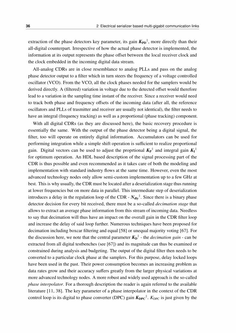
36 2 Electrical serializer based multi-gigabit communication links
extraction of the phase detectors key parameter, its gain KPD‡, more directly than their
all-digital counterpart. Irrespective of how the actual phase detector is implemented, theinformation at its output represents the phase offset between the local receiver clock andthe clock embedded in the incoming digital data stream.
All-analog CDRs are in close resemblance to analog PLLs and pass on the analogphase detector output to a filter which in turn steers the frequency of a voltage controlledoscillator (VCO). From the VCO, all the clock phases needed for the samplers would bederived directly. A (filtered) variation in voltage due to the detected offset would thereforelead to a variation in the sampling time instant of the receiver. Since a receiver would needto track both phase and frequency offsets of the incoming data (after all, the referenceoscillators and PLLs of trasmitter and receiver are usually not identical), the filter needs tohave an integral (frequency tracking) as well as a proportional (phase tracking) component.
With all digital CDRs (as they are discussed here), the basic recovery procedure isessentially the same. With the output of the phase detector being a digital signal, thefilter, too will operate on entirely digital information. Accumulators can be used forperforming integration while a simple shift operation is sufficient to realize proportionalgain. Digital vectors can be used to adjust the proprtional KP
‡ and integral gain KI‡
for optimum operation. An HDL based description of the signal processing part of theCDR is thus possible and even recommended as it takes care of both the modeling andimplementation with standard industry flows at the same time. However, even the mostadvanced technology nodes only allow semi-custom implementation up to a few GHz atbest. This is why usually, the CDR must be located after a deserialization stage thus runningat lower frequencies but on more data in parallel. This intermediate step of deserializationintroduces a delay in the regulation loop of the CDR - Ndly
‡. Since there is a binary phasedetector decision for every bit received, there must be a so-called decimation stage thatallows to extract an average phase information from this stream of incoming data. Needlessto say that decimation will thus have an impact on the overall gain in the CDR filter loopand increase the delay of said loop further. Numerous techniques have been proposed fordecimation including boxcar filtering and equal [58] or unequal majority voting [67]. Forthe discussion here, we note that the central parameter KD
‡ - the decimation gain - can beextracted from all digital testbenches (see [67]) and its magnitude can thus be examined orconstrained during analysis and budgeting. The output of the digital filter then needs to beconverted to a particular clock phase at the samplers. For this purpose, delay locked loopshave been used in the past. Their power consumption becomes an increasing problem asdata rates grow and their accuracy suffers greatly from the larger physical variations atmore advanced technology nodes. A more robust and widely used approach is the so-calledphase interpolator. For a thorough description the reader is again referred to the availableliterature [11, 38]. The key parameter of a phase interpolator in the context of the CDRcontrol loop is its digital to phase converter (DPC) gain KDPC
‡. KDPC is just given by the
2.2 Link system overview and nomenclature 37
number of steps per radian (or bit time UI) that can be performed.
There a two well-established ways in which CDR circuits can be analyzed. The first isto treat the CDR statistically by a Markov chain analysis. This analysis is the preferredchoice in literature about general communication research [60] and takes into accountmost non-linear effects. It is also the way in which some contemporary link budgetingprocedures treat the CDR [60][44].
+BB-PD
KPD
ϕin ϕe+ Decimation/ VotingKV
Kp
AccumulatorKi
PI-Filter
+
Accumulator
Digital tophase conv.KDPC
LoopDelayNdly
ϕout/samp
ϕrx,ref
-
Kp/i digital adjustment(Kp/i,min and Kp/i, range)
Figure 2.13: The (linearized) control loop view of the clock data recovery circuit with annotatedbudgeting parameters
The alternative is to describe the CDR system in phase space. For this to work, all ofits components, even the heavily non-linear BB-PD, have to be linearized. The resultingcontrol loop system can be seen in figure 2.13. The linearization will constrain the validityof the model to well-equalized systems with moderate jitter magnitudes (see section5.3 for details). Its benefit, however, is its general applicability to phase noise spectraldensity analysis (again, see section 5.3) and the straight forward derivation of the relevantbudgeting and specification metrics - the jitter tolerance HCDR,jtol(s) and sometimes thejitter transfer characteristic HCDR,jxfer(s). While the former describes how much input jitterpresent at a particular frequency (thus: the magnitude of the phase noise PSD at the givenfrequency) can be tracked by the CDR loop, the latter is a measure on how much jitter ispassed on to subsequent components in the communication chain if the recovered clock isused and no retiming occurs. This is primarily important for transceiver designs whichoperate as a repeater stage in very long physical communication channels.
Two characteristic functions for CDR performance characterization, the jitter tolerance
38 2 Electrical serializer based multi-gigabit communication links
and jitter transfer functions, can be derived from the CDR loop gain [58]:
HCDR,loop(z) =(KPDKDKDPC
1 − z−1
) (KP +
KI
1 − z−1
)z−Ndly (2.12)
Especially the delay factor z−Ndly makes an analytical treatment of this problem quiteimpossible. Numerical tools and the bilinear transformation can be used to derive the loopgain function in its Laplace form HCDR,loop(s) which we can then use to compute the jittertolerance function to
HCDR,jtol(s) =(1 −
kσj,rx,s
T
)· (1 + HCDR,loop(s)) (2.13)
where σj,rx,s is the total RMS jitter seen at the receiver sampler, k = 2S NR(BER) is twicethe signal to noise ratio required at the target BER level and T is, as usual, the bittime.
The jitter transfer function on the other hand is given by
HCDR,jxfer(s) =HCDR,loop(s)
1 + HCDR,loop(s)(2.14)
These functions do not take into account that the local oscillator itself is jittered, too, andthat the clock distribution of the receiver (which the phase interpolator(s) is obviously apart of) adds further phase noise to the sampling clock as well.
How this circumstance is considered during budgeting together with more details on thevalidity of linearization can be found in section 5.3. To conclude this section, a final remarkon a common metric to describe the performance of a receiver - the receiver sensitivity -has to be made. Again, this is a metric from the rather narrow band radio and microwavefrequency domain. It is defined as the minimal signal strength at the receiver input thatstill leads to an error free operation within the given BER limit:
S min = (S/N)minkBT0
B∫0
NF( f )d f
where (S/N)min is the minimum required signal-to-noise ratio to detect the signal at a givenBER, kB is the Boltzmann Constant, T0 the nominal temperature at receiver input (290 degK), B the bandwidth of receiver and NF( f ) the frequency dependent noise figure of thereceiver.
As described in subsection 2.2.1, this view on sensitivity, which has a voltage signal tonoise ratio in mind, is only a fraction of the information required - in this case the heightof the signal eye at the sampling instant as chosen by the receiver clock recovery circuit.There are, however, more constraints to the operation of a wideband receiver such as thephase noise spectral density of the incoming signal. Also, the residual equalization error of
2.2 Link system overview and nomenclature 39
the signal at the sampler inputs and the residual receiver offset is of importance (a difficulttask once non-LTI equlization schemes such as a decision feedback equalizer (DFE) mustbe included, too ). All of these system imperfections, next to being detrimental to theinput signal itself, lead to a reduction in phase detector gain which in turn degrades theCDR loop bandwidth and thus its capability to track jitter beyond this cutoff effectively.The result is a decrease in eye width which may disallow operation at the target BERlevel. It is due to these very complicated interactions in a system comprised of a sizableamount of subcomponents that an automated and tightly integrated modeling and budgetingmechanism is of the essence, especially as data rates continue to grow and feature sizescontinue to shrink (with thereby growing subcomponent variations). Nevertheless, thereceiver sensitivity metric is of value when channel and transmitter which provide thereference input signal are also known along with the properties discussed in the foregoingparagraphs.
For structural reasons, this text has only hinted at the importance of the transmissionchannel and the equalization stages in the serializer system so far. The next sectionis entirely dedicated to this subject and highlights the fact that it is actually the rangeof supported physical channels that puts the most severe constraints on overall systemarchitecture and the final performance metric, the bit error rate.

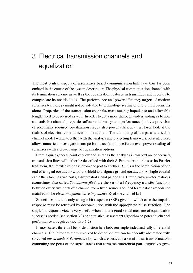
3 Electrical transmission channels andequalization
The most central aspects of a serializer based communication link have thus far beenomitted in the course of the system description: The physical communication channel withits termination scheme as well as the equalization features in transmitter and receiver tocompensate its nonidealities. The performance and power efficiency targets of modernserializer technology might not be solvable by technology scaling or circuit improvementsalone. Properties of the transmission channels, most notably impedance and allowablelength, need to be revised as well. In order to get a more thorough understanding as to howtransmission channel properties affect serializer system performance (and via provisionof potentially required equalization stages also power efficiency), a closer look at therealms of electrical communication is required. The ultimate goal is a parameterizablechannel model which together with the analysis and budgeting framework presented hereallows numerical investigation into performance (and in the future even power) scaling ofserializers with a broad range of equalization options.
From a quiet general point of view and as far as the analyses in this text are concerned,transmission lines will either be described with their S-Parameter matrices or its Fouriertransform, the impulse response, from one port to another. A port is the combination of oneend of a signal conductor with its (shield and signal) ground conductor. A single coaxialcable therefore has two ports, a differential signal pair of a PCB four. S-Parameter matrices(sometimes also called Touchstone files) are the set of all frequency transfer functionsbetween every two ports of a channel for a fixed source and load termination impedancematched to the electromagnetic wave impedance Z0 of the channel [51].
Sometimes, there is only a single bit response (SBR) given in which case the impulseresponse must be retrieved by deconvolution with the appropriate pulse function. Thesingle bit response view is very useful when either a good visual measure of equalizationsuccess is needed (see section 3.3) or a statistical assessment algorithm on potential channelperformance is required (see also 5.2).
In most cases, there will be no distinction here between single ended and fully differentialchannels. The latter are more involved to described but can be decently abstracted withso-called mixed mode S-Parameters [3] which are basically a set of linear transformationscombining the ports of the signal traces that form the differential pair. Figure 3.5 gives
41

42 3 Electrical transmission channels and equalization
an example of a channel described by both its forward transfer function (from one end ofthe cable to the other) and the associated SBR. The SBR in figure 3.5 is normalized intime to the unit interval T of the bit pulse with which it was created. Ideally, there wouldonly be a signal unequal to zero at the so-called main cursor t = 0 · T . However, due tothe dispersive (group delay) and lossy properties of the channel, there is a residual signalat time instants t = n · T . Other bits which are transmitted at these instants in time havetheir main cursor voltage superimposed with these perturbations which is why this effect iscalled intersymbol interference (ISI).
-3 -2 -1 0 1 2 3 4 5 6 7 8 9 10 11 12 13 14 15 16 17 18 19 20 21 22 23 24 25 26 27 28 29 30-0.05
0
0.05
0.1
0.15
0.2
0.25
Tap Position (UI)
Nor
mal
ized
Pul
se r
espo
nse
mag
nitu
de
Pk Dist: 3.271
0 5e+09 1e+10 1.5e+10 2e+10 2.5e+10 3e+10-40
-30
-20
-10
0
Frequency (GHz)
Res
pons
e M
agni
tude
(dB
)
IL upper bound - CEI-25G-LRIL lower bound
Figure 3.1: SBR at UI=40 ps and frequency response of a 25 Gigabit worst case CEI-25G-LRcomposite channel from ECAD generated S-Parameter data (compliance mask shown in dashedlines)
As can be guessed from figure 3.1 already, a closed form equation to describe thefrequency transfer characteristic is very hard to find analytically. Oftentimes and especiallyat higher frequencies, the connectors, landing pads of coupling capacitances or even the
43
package balls of a chip or die pose enough of a physical discontinuity to severely changethe wave impedance for a small section of the physical channel. At the spatial location ofthe impedance discontinuities, a part of the incident signal power of the electromagneticwave is reflected. Its magnitude depends on the magnitude of impedance mismatch andthe scattered electromagnetic wave then travels down the transmission line in oppositedirection. This is also one of the reasons for using source end termination and why it hasto be matched to the wave guide impedance: the termination serves as an absorber forbackreflected electromagnetic waves. Signal power which is reflected 2N times within thechannel and which is thus travelling towards the receiver once more, must naturally travela longer distance to arrive at the receiver input. This portion of the signal reveals itself asadditional ISI at tap locations very far away from the main cursor (see tap 24 and 25 of theSBR in figure 3.1). Pairs of discontinuities may form a filter for particular wavelengthsdepending on their spatial separation and the wave propagation velocity in between them.They reflect in the sporadic, periodically spaced dips of the transfer function as can also beseen in figure 3.1).
Instead of analyzing a transmission channel in terms of its frequency response by usinga vector network analyzer for instance, one can also use a time domain reflectometer(TDR). It reveals the location of discontinuities within a transmission channel by sendinga step function of well defined rise-time into the channel under test. It then records thesignal waveform incident on its own output and recomputes the waveguide impedance inrelation to the time passed since sending out the initial step. Figure 3.2 shows the resultof such a measurement for the channel whose frequency response and SBR are given infigure 3.1. A commercial ECAD tool was used for this purpose which mimics the TDRprocess numerically. One can see that in order to obtain the discontinuities, the channelwas designed to feature different sections of waveguides as they would also appear in atypical HPC network link for instance (compare figure 2.4 of section 2.2.3). All sectionsthemselves (except for the discontinuities) have a differential impedance of 100Ω. Thereis a section of package trace right after the chip followed by the discontinuity due tothe cross over from package to PCB with landing pad and chip balls (assuming a flipchip arrangement). The very small traces of the package exhibit a strong skin-effect andconductor loss (see below) and thus lead to a sharp increase in computed impedance. Thestrong discontinuity makes the PCB waveguide section appear a lot more low ohmic than itreally is. There is a further discontinuity from PCB to the AWG interconnect cable due tothe cable connector and its landing pads. The middle of the channel then is the symmetryplane of the interconnect.
In essence, while for general considerations and design space exploration simple channelmodels based on analytic equations are perfectly suitable, serializer verification andbudgeting frameworks need to work with true S-Parameter based channels, too, in order tocapture the various effects that may be detrimental to signal quality at the receiver input.

44 3 Electrical transmission channels and equalization
Time delay (ns)
130
120
110
100
90
80
7014121086420
Diff
. Im
peda
nce
(Ohm
s)
Line of SymmetryAWG-32 coaxial cablePCBPackage PCB Package
Discontinuities
Figure 3.2: TDR simulation of the transmission channel with transfer function as given in figure3.1 exhibiting various discontinuities responsible for the resonances
Examples of toplevel design space exploration profiting from a simple numeric channelmodel are given by papers which deal with feasibility and energy efficiency of exascaleHPC systems (such as [29] and [59]). They usually use the so-called bit rate capacityof a physical, electrical transmission channel to express and predict I/O performance interms of system size and integration density, i.e., to arrive at scaling laws for area costof communication. An introduction on how this metric is derived will be given belowalong with an explanation of its particular shortcomings and problems when it comes toestimating the performance of modern serializer based communication schemes. Thismotivates the introduction of the Johnson signal model for coaxial transmission lines asdescribed thereafter. This model can then already be used to derive bit rate capacity scalinglaws for comparison with previous work, even without an actual serializer system model.
3.1 The bitrate capacity
In a paper from 1997, Miller and Ozaktas introduce the concept of a so called bitratecapacity of a channel [36] which is defined to be the upper limit of data transmissioncapability when no equalization or signal refresh is applied. By starting with a coaxial line(due to its relative mathematical simplicity) and by arguing that scaling other transmissionchannel types such as microstrip and stripline geometries would basically adhere to thesame kind of physical constraints for reasonable sizing, they derive a general equation for
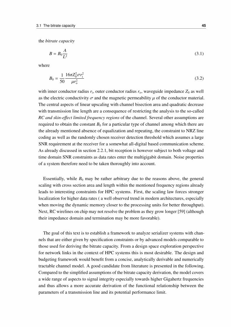
3.1 The bitrate capacity 45
the bitrate capacity
B = B0AL2 (3.1)
where
B0 =150
16πZ20σr2
i
µr2o
(3.2)
with inner conductor radius ri, outer conductor radius ro, waveguide impedance Z0 as wellas the electric conductivity σ and the magnetic permeability µ of the conductor material.The central aspects of linear upscaling with channel bisection area and quadratic decreasewith transmission line length are a consequence of restricting the analysis to the so-calledRC and skin-effect limited frequency regions of the channel. Several other assumptions arerequired to obtain the constant B0 for a particular type of channel among which there arethe already mentioned absence of equalization and repeating, the constraint to NRZ linecoding as well as the randomly chosen receiver detection threshold which assumes a largeSNR requirement at the receiver for a somewhat all-digital based communication scheme.As already discussed in section 2.2.1, bit reception is however subject to both voltage andtime domain SNR constraints as data rates enter the multigigabit domain. Noise propertiesof a system therefore need to be taken thoroughly into account.
Essentially, while B0 may be rather arbitrary due to the reasons above, the generalscaling with cross section area and length within the mentioned frequency regions alreadyleads to interesting constraints for HPC systems. First, the scaling law forces strongerlocalization for higher data rates ( a well observed trend in modern architectures, especiallywhen moving the dynamic memory closer to the processing units for better throughput).Next, RC wirelines on chip may not resolve the problem as they grow longer [59] (althoughtheir impedance domain and termination may be more favorable).
The goal of this text is to establish a framework to analyze serializer systems with chan-nels that are either given by specification constraints or by advanced models comparable tothose used for deriving the bitrate capacity. From a design space exploration perspectivefor network links in the context of HPC systems this is most desirable. The design andbudgeting framework would benefit from a concise, analytically derivable and numericallytractable channel model. A good candidate from literature is presented in the following.Compared to the simplified assumptions of the bitrate capacity derivation, the model coversa wide range of aspects to signal integrity especially towards higher Gigahertz frequenciesand thus allows a more accurate derivation of the functional relationship between theparameters of a transmission line and its potential performance limit.
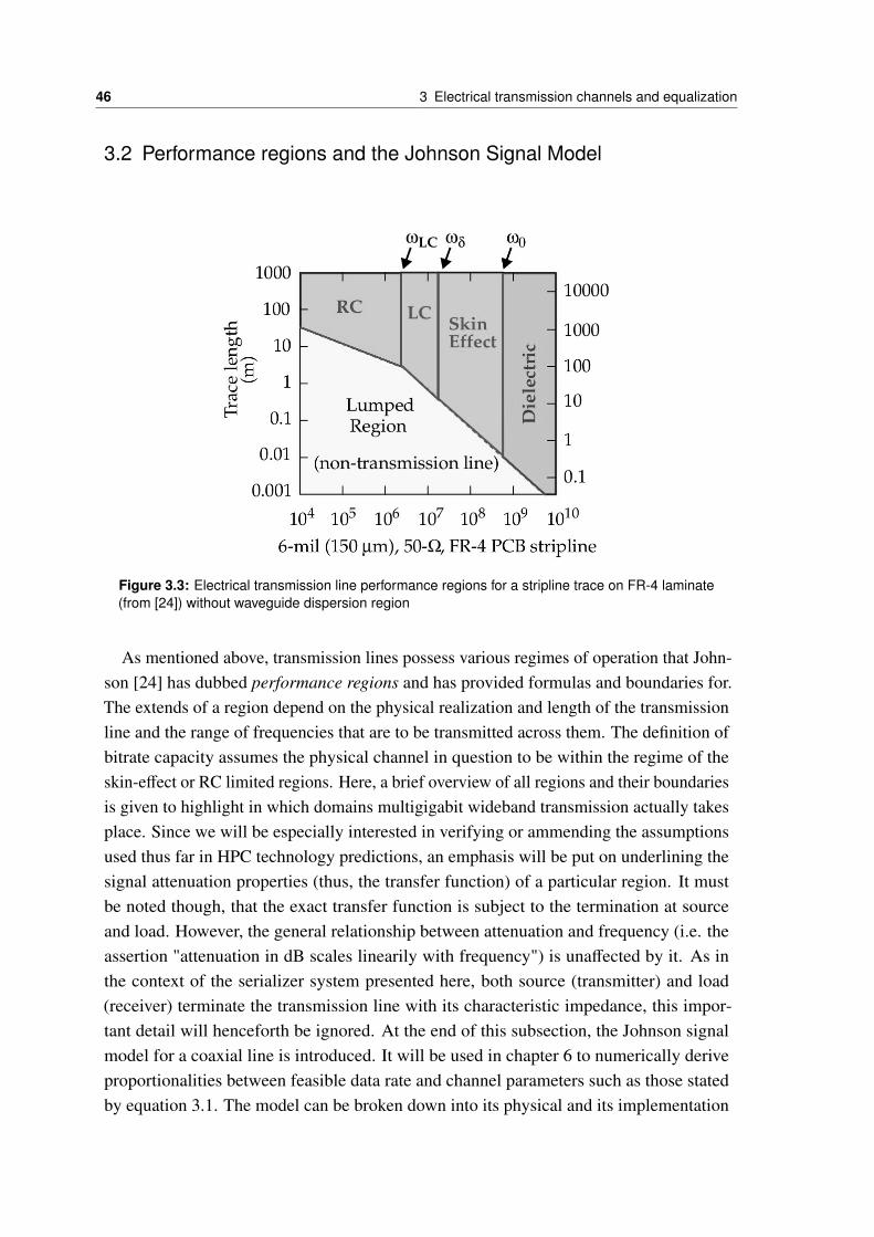
46 3 Electrical transmission channels and equalization
3.2 Performance regions and the Johnson Signal Model
Figure 3.3: Electrical transmission line performance regions for a stripline trace on FR-4 laminate(from [24]) without waveguide dispersion region
As mentioned above, transmission lines possess various regimes of operation that John-son [24] has dubbed performance regions and has provided formulas and boundaries for.The extends of a region depend on the physical realization and length of the transmissionline and the range of frequencies that are to be transmitted across them. The definition ofbitrate capacity assumes the physical channel in question to be within the regime of theskin-effect or RC limited regions. Here, a brief overview of all regions and their boundariesis given to highlight in which domains multigigabit wideband transmission actually takesplace. Since we will be especially interested in verifying or ammending the assumptionsused thus far in HPC technology predictions, an emphasis will be put on underlining thesignal attenuation properties (thus, the transfer function) of a particular region. It mustbe noted though, that the exact transfer function is subject to the termination at sourceand load. However, the general relationship between attenuation and frequency (i.e. theassertion "attenuation in dB scales linearily with frequency") is unaffected by it. As inthe context of the serializer system presented here, both source (transmitter) and load(receiver) terminate the transmission line with its characteristic impedance, this impor-tant detail will henceforth be ignored. At the end of this subsection, the Johnson signalmodel for a coaxial line is introduced. It will be used in chapter 6 to numerically deriveproportionalities between feasible data rate and channel parameters such as those statedby equation 3.1. The model can be broken down into its physical and its implementation
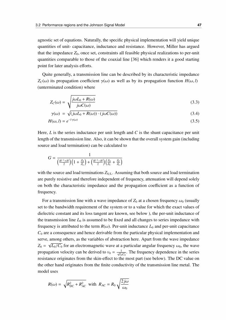
3.2 Performance regions and the Johnson Signal Model 47
agnostic set of equations. Naturally, the specific physical implementation will yield uniquequantities of unit- capacitance, inductance and resistance. However, Miller has arguedthat the impedance Z0, once set, constraints all feasible physical realizations to per-unitquantities comparable to those of the coaxial line [36] which renders it a good startingpoint for later analysis efforts.
Quite generally, a transmission line can be described by its characteristic impedanceZC(ω) its propagation coefficient γ(ω) as well as by its propagation function H(ω, l)(unterminated condition) where
ZC(ω) =
√jωL0 + R(ω)
jωC(ω)(3.3)
γ(ω) =√
( jωL0 + R(ω)) · ( jωC(ω)) (3.4)
H(ω, l) = e−l·γ(ω) (3.5)
Here, L is the series inductance per unit length and C is the shunt capacitance per unitlength of the transmission line. Also, it can be shown that the overall system gain (includingsource and load termination) can be calculated to
G =1(
H−1+H2
) (1 + ZS
ZL
)+
(H−1−H
2
) (ZSZC+ ZC
ZL
)with the source and load terminations ZS/L. Assuming that both source and load terminationare purely resistive and therefore independent of frequency, attenuation will depend solelyon both the characteristic impedance and the propagation coefficient as a function offrequency.
For a transmission line with a wave impedance of Z0 at a chosen frequency ω0 (usuallyset to the bandwidth requirement of the system or to a value for which the exact values ofdielectric constant and its loss tangent are known, see below ), the per-unit inductance ofthe transmission line L0 is assumed to be fixed and all changes to series impedance withfrequency is attributed to the term R(ω). Per-unit inductance L0 and per-unit capacitanceC0 are a consequence and hence derivable from the particular physical implementation andserve, among others, as the variables of abstraction here. Apart from the wave impedanceZ0 =
√L0/C0 for an electromagnetic wave at a particular angular frequency ω0, the wave
propagation velocity can be derived to v0 =1
√L0C0
. The frequency dependence in the seriesresistance originates from the skin-effect to the most part (see below). The DC value onthe other hand originates from the finite conductivity of the transmission line metal. Themodel uses
R(ω) =√
R2DC + R2
AC with RAC = R0
√2 jωω0
48 3 Electrical transmission channels and equalization
to describe the general development. Again, RDC and R0 form the layer of abstraction forthe physical implementation. The square root function models a smooth cross-over fromthe DC resistance dominated regime to the inductively dominated regimes. Finally, thedependence of the per-unit capacitance on frequency which is primarily due to the changesin dielectric permittivity with frequency are modelled as
C(ω) = C0
(jωω0
)− 2θ0π
(3.6)
where the loss tangent θ0 ≈ tan(θ0) =(−εiεr
)specifies the relation between real and imaginary
part of the dielectric permittivity of the material surrounding the center conductor at thegiven angular frequency ω0. With these geometry independent functions in mind, thevarious performance regions and their limits can thus be defined. Depending on thegeometry of an electric channel and the particular frequency band of operation there arethe following performance regions of an electric transmission line:
3.2.1 Lumped Element Region
In this region, the length L of the transmission line is small enough so that the effectsof distributed parasitic elements can safely be ignored. The transmission line can thenbe described as the equivalent of a Pi-Model in which all parasitic effects of the line arelumped into a single inductive, resistive and two capacitive elements (hence the name).This is the case when the magnitude of the exponent of the propagation function H(ω, l)remains lower than a constant ∆, typically set to a value of about 0.25 nepers (2.17 dB),that is
|lγ(ω)| < ∆
Since γ is a function monotonously increasing with ω, the inequality only needs to bechecked for the transmission line of greatest extent at the maximum frequency within agiven system. It can be shown that for an ideal, unloaded source (no source resistance,infinite load resistance), the resulting propagation function is approximately given byH = 1
2+(lγ) .In other words: as long as the transmission line is short enough to be considered
"lumped", there is no spectrally distorting effect on the signal it carries. Its impact liessolely in the very slight attenuation of about 0.968 at the boundary of the region. Thiscorresponds to a loss of roughly 0.3dB at the given length.
As can be seen in figure 3.3 a crossover from the lumped element region can occur eitherto the RC dominated or LC dominated domain, depending on operating frequency andlength of the transmission line. Therefore, the maximum effective length a transmission
3.2 Performance regions and the Johnson Signal Model 49
line that may safely be described as a lumped element can either be
l ≈∆
√ωRDCC
when RDC > ωL or l ≈∆
ω√
LCwhen RDC < ωL
Here, RDC is the DC resistance of the transmission line (and its current return path) and ∆arbitrarily chosen just like above. Physically speaking, the first case then demands thatthe lumped cut-off angular frequency of the RC transmission line fco =
1l2RDCC needs to be
at least 1∆2 = 16 times higher than the maximum angular frequency ω of the signal to be
transmitted. Similarly, the second case can be interpreted as the requirement of having anLC delay lγ = l
√LC 16 times smaller than 1
ω.
In this text, we are interested in how the attenuation (or equivalently put, the loss) of atransmission line changes with its most decisive feature: its length (and to some degreewith its bisectional area as well). As the term lumped, however suggests, there is not muchpractical information to be gained here, as either the frequencies of operation are of onlylittle interest to a multigigabit serializer or the extends of the transmission line itself aremuch too small. This will be much different for the regions to follow.
3.2.2 RC Region
The RC or dispersive region stretches from DC to (potentially) several MHz and requiresthat the extends of the transmission line are significant with respect to the wavelengthscontained in the signals to be transmitted. The transmission line is then described as aseries of small resistor-capacitor low pass elements as it is usually done in integrated circuitdesign for frequencies of several hundreds of MHz at larger technology nodes. Towardshigher frequencies, this region ends as soon as the per-unit series inductance ωL becomescomparable in magnitude to the per-unit DC resistance of the transmission line, that is
ωLC =RDC
L(3.7)
Similar to the length boundary definition for the lumped element region, the length belowwhich there is no significant distributed RC behavior can be derived to
lRC =∆
RDC
√LC
and is thus determined by the ratio between transmission line impedance and unit-lengthDC resistance. For long-haul channels in high quality cables and even for ordinary printedcircuit boards traces shorter than one meter, the DC resistance is usually much smallerthen the characteristic impedance (quite often 40 − 80Ω making the RC region ratherunimportant at these scopes. Due to the small bisection of on-package or on-die wiring
50 3 Electrical transmission channels and equalization
and especially with the advent of 3D through silicon via stacking, this region is however ofnoticeable importance to future short-haul multigigabit I/O standards.
In case of a low impedance source and a perfect termination ZL = ZC, the system transferfunction G will read G(ω,l) = e−l
√jωRC and it can be seen that the logarithm of signal
attenuation will scale with the inverse of the square root of frequency. The rather commoncase of termination with a purely resistive value chosen in accordance with the waveimpedance ZL = Z0 of the line produces a much more involved equation which requiresnumerical processing and analysis.
3.2.3 LC Region
If the frequency of operation is increased beyond the point at which the inductive propertiesof the transmission line are less significant than its resistive properties as suggested byequation 3.7, the interconnection is said to be operated in the LC or constant loss region.Due to the physical dimensions of commonly used transmission lines within an electronicsystem (be it on die, within packages or on PCBs), this region with its constant loss versusfrequency property is very narrow and often totally absorbed by the succeeding skin-effectregion [24].
3.2.4 Skin-effect Region
As the frequency of operation is increased further, the eddy currents within the body of theconductors will limit the flow of charge carriers to a shallow region at the perimeter of theconductors. The so-called skin-depth, the thickness of the layer of metal at the surface ofthe conductor where the current will flow can be shown to adhere to
δ =
√2ωµσ
The effective series resistance seen at higher frequencies RAC(ω) will therefore continuouslyincrease with frequency. Ignoring more subtle effects (linear correction factors due tosurface roughness and conductor proximity effects), the low frequency magnitude is
R0 ∝1
pδσ
where again, p is the perimeter of the conductors in question. Quite obviously, the onsetof this region depends greatly on the physical realization of the transmission line. Again,ignoring the subtle correction factors, an estimate is given by
ωδ =2µσ
( pa
)2(3.8)

3.2 Performance regions and the Johnson Signal Model 51
where µ is the conductors magnetic permeability constant, σ its conductivity, p the perime-ter of the conductor and a its cross sectional area. Since it can be shown that the propagationcoefficient γ(ω) is proportional to the square root of frequency, the logarithmic signalattenuation itself, too, will exhibit a (inverse) square root dependency with frequency. ForI/O standards operating in the regime of several hundreds to some thousands of MHzacross packages and PCBs, the skin-effect region is the primary region of operation to beconsidered - as Millers analysis of the bit-rate capacity [36] also underlines.
3.2.5 Dielectric loss Region
As the electromagnetic wave progresses on the transmission line, it will inevitably interactwith the surrounding dielectric material. This interaction can both take place on a molecularand atomic level depending on the angular frequency of the wave and stimulates a specificdegree of freedom in the solid state body of the dielectric. Consequently, there is a transferof energy from electromagnetic wave to the dielectric taking place. As frequency increases,so does the complex function of relative dielectric permittivity. The phase angle between itsreal and imaginary parts - the loss tangent, however, stays very constant over a broad rangeof frequencies. It can thus be shown that equation 3.6 produces a good estimation of thegeneral process 1. It can further be shown that the real part of the propagation coefficientwhich produces the attenuation component in the transfer function can be derived to
Reγ(ω) =12θ0ω
v0
(ω
ω0
)−θ0/πfrom which it can be seen that dielectric loss increases signal attenuation on a logarithmicscale in proportion to frequency. Therefore, the cross-over range from skin-effect dom-inated to dielectric loss dominated region is very broad. Mathematically, the boundarycan be specified by comparing the attenuation magnitudes caused by either effects anddetermining the frequency, where the contributions to overall signal attenuation are equal.This gives
ωθ =1ω0
(v0R0
Z0θ0
)2
It must be noted though that due to the difference in proportionality to frequency betweenskin-effect and dielectric effect, already at a frequency ten times lower than ωθ, thedielectric contribution to overall attenuation already is about one fourth! This aspect isespecially important for the discussion of highly integrated transmission lines of very small
1 Modelling the complex relative permittivity correctly is quite involved and failure to enforce a stringent relationbetween its real and imaginary parts for all frequencies will produce transfer functions which can be nonreal or evennoncausal.
52 3 Electrical transmission channels and equalization
dimensions. Naturally, their wave impedance needs to be rather low while their perimeterp is very small. This makes skin-effects look very dominant while pushing the value forωθ to fairly high frequencies (compare table 3.4 ). Due to the broad transition betweenthe two performance regions, however, neglecting the dielectric effect will produce overlyoptimistic results.
3.2.6 Waveguide dispersion region
As soon as the electromagnetic wavelengths become comparable to conductor dimensions,electromagnetic field modes other than the regular TEM mode may also propagate on thetransmission line. This linear superposition of modes can lead to phase distortion sincethe group delay of each mode may be very different. The onset frequency for non-TEMmodes mostly depends on the physical geometry of the waveguide. For the cases of highintegration and small cross-sectional dimension discussed here, however, this region cansafely be ignored even for the years to come. Table 3.4 still lists values as a reference forsome of the test channels used in this text.
3.2.7 Johnson Signal Model for a coaxial transmission line
The various different performance regions owe their existence to distinct physical effectsgaining importance over others as frequency increases. Johnson proposed a set of equationswhich are suitable to describe a transmission line from DC up to the regime of 10 GHzwith good accuracy [24] consistently covering all of the above mentioned regions exceptfor the last. Although the model itself is not limited to a specific physical realization, thecoaxial cable is chosen here due to its analytic tractability and comparability to what hasbeen introduced by Miller et al. when defining the bit rate capacity.
In order to simplify the analysis in chapter 6, the free model parameters are constrainedto a smaller set and the way in which (physical) parameters are fixed is explained below.The remaining free arguments of the model will be
• The target impedance Z0
• The real part of the dielectric permittivity εr and
• Its loss tangent θ0
• The frequency ω0 at which the complex dielectric permittivity ε (and from it thefrequency independent loss tangent θ0 ), the magnetic permeability µ of the dielectricmaterial and therefore Z0 are defined. µ, however, is fixed to unity here.
• The length L of the channel
• The radius a of the coaxial cables inner conductor

3.2 Performance regions and the Johnson Signal Model 53
The conductivity σCu of center and shield (reference plane) conductor are constrained tothe value of annealed copper at 20 C which is 5.87 · 107 S
m .Note that one of the major reasons for the limited usefulness of the model towards very
high frequencies originates from the rather simple dielectric model. At higher frequencies,the dielectric permittivity is a very much nonlinear function of frequency both in its realand imaginary parts and depends on the atomistic properties of the dielectric material itself.Especially the real part of the function can only be considered constant up to very lowGHz regions where electromagnetic absorption processes by electric dipoles or molec-ular degrees of freedom can not be stimulated by the wavelengths of the propagating signal.
The geometry of the coaxial cable is shown on the left of figure 3.4. With the innerradius a given, we constrain the sheet conductor thickness d of the shielding conductor tothe same value. For analysis of the dependence of system performance on cabling area A,the conductor bisectional area is calculated according to
A = π · (b + 2d)2
It can be shown that for a coaxial line, the per-unit capacitance and the per-unit inductanceare
C0 =2πεεr
ln(b/a)and L0 =
µ0µ
2πln(b/a)
respectively. With Z0 =
√L0C0
given, the outer radius b of the cable is then constrained to
b = aeZ0χ with χ =
√µ0µ
4π2ε0ε
Apart from the prefactor of 12π due to the coaxial geometry and the material constants of
the dielectric separating inner and outer conductor, χ looks quite like the definition of thefree space wave impedance. It can directly be seen, why cables for high-density intercon-nections need to posses very low dielectric constant to limit the bisectional area. Also,high-impedance wiring beyond the standard 50Ω which could reduce current consumptionin transmitter output buffers and terminations, lead to an increase in bisection area and thuspose a challenge to high integration requirements. Additionally and as a consequence ofhigher area demand, high impedance transmission lines are also more susceptible to crosstalk and generally electromagnetic coupling. For this reason and also due to increasingintegration densities in PCBs, the trend of recent years has even been towards lower lineimpedances (such as 40Ω in PCI- Express [14]). This, of course, is in notable contrastto what would be advisable from equation 3.2 for the bit rate capacity which increaseslinearily with Z0.

54 3 Electrical transmission channels and equalization
The DC resistance of the coaxial transmission line is given by
RDC =1σCu
(1πa2 +
12πd · b
)i.e. the inverse of the bisectional area of rugged center and a sheet shield conductormultiplied with the metals conductivity. For the low frequency value of AC ResistanceR0, we ignore surface roughness for the time being, setting kr = 1. While this should be agood choice for coaxial cables, it is rather optimistic for traces on printed circuit boards- apart from the fact that feasible geometries on multilayer circuit boards are not all thatwell described with a coaxial approach. The proximity coefficient kp (for details, refer to[24]) can be calculated to
kp =
(1 +
ab
)which thus gives
R0 = kp · kr ·1
pσδ=
(1 +
ab
) 12πa
√ω0µ
2σCu
To arrive at the values for the onset of non-TEM modes as given in table 3.2, we choosethe earliest of these modes (TE11, again compare [24]) which is calculated with
fc =ckc
2π√
er
where the geometry dependent quantity kc is the so-called wave number given by kc =2
a+b
for a coaxial cable.
a
db
Coaxial Stripline
tw s
bt
w sb
εair
Microstrip
εpassεdiel εdiel
εdiel
Figure 3.4: Common channel topologies as encountered in typical HPC systems, coax shown insingle ended, stripline and microstrip in differential configuration
For the remainder of this text, there will be two different approaches to define and use

3.2 Performance regions and the Johnson Signal Model 55
channel models. The analytic model presented here is used to derive scaling trends forserializer based links in close resemblence to what has been done in the context of bitrate capacity (chapter 6). For the actual verification and budgeting of serializer systems,however, we require less idealized channels. They need to be composed of various sectionsrepresenting the different waveguide geometries encountered in a typical network link(compare figure 2.4 of subsection 2.2.2 and figure 3.4). These sections are
• The package breakout section - very narrow and thin traces contained in layeredceramic or organic material and covered by reference planes to either side. This isalso called a stripline geometry and it is clear from figure 3.4 that the electromagneticfieldlines surrounding the center conductor(s) will be vastly different from the coaxialcase.
• The printed circuit board section - usually featuring much wider but not much thickersignal conductors and likely not to be entirely implemented as striplines. Due topotential AC coupling capacitors or connectors, there may have to be sections ofmicrostrip lines with far less favorable wave guide properties, too. This is especiallytrue due to the various dielectric constants of laminate, passivation and air that willbe penetrated by the electromagnetic waves of the center conductor(s)
• The cable section - usually a coaxial cable of rather small bisectional area due tohigh integration demands
• Impedance discontinuities between all above mentioned sections which are due topackage balls, component landing pads of packages, capacitors and connectors aswell as due to vias for the interconnection between the various layers at which signalconductors reside.
Unlike coaxial geometries, stripline and microstrip transmission lines are far more involvedto model. Additional effects such as surface roughness and the frequency dependence ofthe dielectric permittivity add to the complexity of more advanced models. Commercialcomputer aided design (CAD) vendors for microwave and RF software put considerableeffort in these types of models. Also, in modern serializer design, all interconnects areusually routed in a differential, coupled topology to provide better EMI and crosstalkimmunity in high density applications. This is indicated in figure 3.4 for microstrip andstripline and further adds to the overall complexity of the underlying equations. The closeproximity of the two center conductors which carry the same signal with opposite polarityleads to an additional coupling capacitance between them and the resulting wave guideimpedance will effectively be lowered. The details of differential signalling are beyond thescope of this text and it will be sufficient here to note the general derivability of so-calledmixed mode S-Parameters from their bare single-ended counterparts.
56 3 Electrical transmission channels and equalization
It is for these reason that for serializer analysis and budgeting we choose to use modeldata generated with advanced CAD programs. The standard output of these modellingprocesses are the S-Parameter matrices as mentioned at the beginning of this section whichcan then be preprocessed and used within the simulation framework presented in the nextchapter.
Since there would be a vast variety of parameters and implementation possibilities toarrive at very different transfer functions, the industry has agreed on certain standards totest transmission channels for compliance, that is: general suitability for a well-definedpurpose. These standards are either given in the form of a frequency mask such as thedashed lines in the exemplary frequency transfer function plots below (figures 3.6 and3.7) or - in the past and nowadays rather uncommon - in the form of pulse or impulseresponses. The former is the case with the Optical Internetworking Forum (OIF) commonelectrical I/O (CEI) standard [46], an example for the latter is the 10G Ethernet standard[17]. Finally, a third alternative is to avoid any explicit channel compliance definition bydemanding a channel to plainly allow operation at a specifc BER level with the transmitterand receiver electrical specifications of the standard. Such is the case for lower speed CEIchannels and PCI-E 3.0 [14]. Compliance is then checked for the entire system against aso-called eye mask, usually a diamond shaped representation of the eye opening in termsof eye width and eye height at the defined BER level.
In the following, we will be working with four distinct channels depending on thescope of investigation. For lower frequency budgeting investigations, the 10G Ethernetreference channel (the specification refers to it as stressor) is used. It is defined in termsof its impulse response from which the frequency transfer function and the SBR can becomputed. Both are shown in figure 3.5.
At higher frequencies, the CEI specifications for 25 Gbps long reach channels are usedfor orientation. The Johnson signal model is used to produce a worst case channel responsefor two different scenarios:
Both Johnson signal model channels have an impedance of Z0 = 50Ω single-endedlyand feature no coupling between the traces.
• The PCB type channel is shown in figure 3.6 and has a parameter set as listed in table3.2. Due to its comparably high loss tangent and small center conductor radius, it islimited to a length of about 700 mm.
• The American Wire Gauge (AWG) type channel is shown in figure 3.7 and has aparameter set as listed in the second row of table 3.2. Due to the very low losstangent and bigger center conductor radius, within the given constraint mask it canstill span 2.5 m. The onset frequency of the dielectric region ωθ is lower for the AWGchannel even though the loss tangent θ0 is smaller than for a PCB-type realization.This is because R0 decreases at the same time even more drastically due to the larger
3.2 Performance regions and the Johnson Signal Model 57
perimeter of the center conductor. It must, however, again be stressed here that ωθ isonly a measure of relative dominance between skin and dielectric loss magnitudes.As such, it is only an indicator of the relative importance each effect has for the datarate to be transmitted across this channel.
The well-known consequence of the numbers in table 3.4 thus is that dielectric effectsare an increasing issue as data rates approach the tens of gigabits per second, even moreso if the transmission channel (even partially) consists of printed circuit board traces.As metioned, this aspect is even further amplified by the fact that the coaxial line andits corresponding field distribution is a very optimistic approximation of realizable PCBchannel structures.
Additionally, a commercial ECAD tool is used to construct a fully differential channel ofZdi f f 0 = 100Ω with the above mentioned sections and intentional discontinuities betweenthem where the values for the various sections of package and PCB substrate and thesize of interconnect wiring between the two endpoints (compare figure 2.4) is chosen inaccordance with commercially available, advanced manufacturing constraints. Figure 3.1at the beginning of this section shows the according SBR and transfer function where theresonances of the discontinuities are clearly visible. Additionally, the TDR measurementof figure 3.2 highlights the various different sections of the communication channel andvisualizes the discontinuities in time (and thus space) domain.
Channel f0 = ω0/2π εr θ a L
CEI25G-LR in PCB 1 GHz 3.5 (improved FR4) 0.007
√WtypTtypπ=√
100 um17 umπ
= 23.3 um0.686 m
CEI25G-LR in 32-AWG 1 GHz 2.0 (FPE dielectric) 0.0028 100 um 2.5 m
Table 3.2: Parameters of the Johnson Signal Model for the PCB-type and AWG-type coaxialcables used in this text
Channel Name LC Skin Dielectric TE11 3dB cutoff 30dB cutoff
CEI25G-LR in PCB 5.71 MHz 26.92 MHz 24.8 GHz 380 GHz 430 MHz 16.6 GHz
CEI25G-LR in 32-AWG 430 kHz 1.36 MHz 17.14 GHz 158.75 GHz 480 MHz 16.5 GHz
Table 3.4: Approximate region boundaries with respect to frequency for the two Johnson signalmodel test channels presented here.
58 3 Electrical transmission channels and equalization
-4 -3 -2 -1 0 1 2 3 4 5 6 7 80
0.05
0.1
0.15
0.2
0.25
0.3
0.35
0.4
0.45
0.5
Tap Position (UI)
Pul
se r
espo
nse
mag
nitu
de
Pk Dist: 1.158
0 2e+09 4e+09 6e+09 8e+09 1e+10-40
-30
-20
-10
0
Frequency (GHz)
Res
pons
e M
agni
tude
(dB
)
Figure 3.5: SBR at UI=100 ps and frequency response of a 10 Gigabit Ethernet reference channel

3.2 Performance regions and the Johnson Signal Model 59
-3 -2 -1 0 1 2 3 4 5 6 7 8 9 10 11 12 13 14 15-0.05
0
0.05
0.1
0.15
0.2
0.25
Tap Position (UI)
Nor
mal
ized
Pul
se r
espo
nse
mag
nitu
de
Pk Dist: 2.792
0 5e+09 1e+10 1.5e+10 2e+10 2.5e+10 3e+10-40
-30
-20
-10
0
Frequency (GHz)
Res
pons
e M
agni
tude
(dB
)
IL upper bound - CEI-25G-LRIL lower bound
Figure 3.6: SBR at UI=40 ps and frequency response of a 25 Gigabit worst case CEI-25G-LRPCB channel (compliance mask shown in dashed lines)
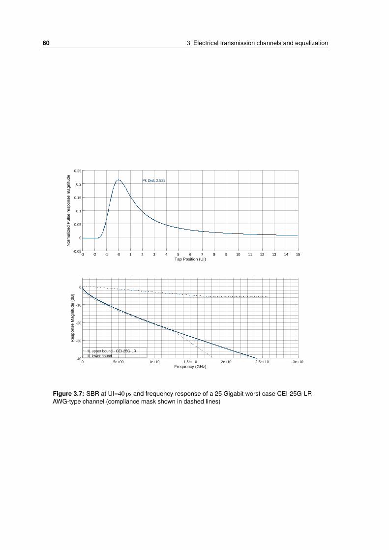
60 3 Electrical transmission channels and equalization
-3 -2 -1 -0 1 2 3 4 5 6 7 8 9 10 11 12 13 14 15-0.05
0
0.05
0.1
0.15
0.2
0.25
Tap Position (UI)
Nor
mal
ized
Pul
se r
espo
nse
mag
nitu
de
Pk Dist: 2.828
0 5e+09 1e+10 1.5e+10 2e+10 2.5e+10 3e+10-40
-30
-20
-10
0
Frequency (GHz)
Res
pons
e M
agni
tude
(dB
)
IL upper bound - CEI-25G-LRIL lower bound
Figure 3.7: SBR at UI=40 ps and frequency response of a 25 Gigabit worst case CEI-25G-LRAWG-type channel (compliance mask shown in dashed lines)
3.2 Performance regions and the Johnson Signal Model 61
Without knowing much more details about the actual serializer system to be used, theJohnson signal model only preliminarily allows to derive some first estimations on howdata rates may actually scale with transmission line properties. For this purpose we firstnote that the equalization efforts presented in the next subsection do not substantiallyelevate the signal level at the Nyquist frequency. For the moment, we therefore assumethe receiver to be capable of still resolving the incoming data stream as long as channelattenuation does not fall below a given threshold level. In light of the publications in recentyears, we set this limit in attenuation to 20 log10|H(ω)| = −30 dB. The Johnson signalmodel for the coaxial line can then be used to compute the 30 dB cutoff frequency for agiven set of parameters. For figures 3.8 to 3.10, the impedance Z0, the length L and thebisectional area A (via inner conductor radius ri) are tuned respectively, while the otherparameters are fixed at ω0 = 1 GHz, εr = 3.5 and θ0 = 0.007 to reflect a more advancedbut not too expensive PCB board material. The plot trace is colored red whenever thedielectric realm dominates over the skin-effect, it is colored grey whenever the skin-effectis more important in magnitude.
From this standpoint, the following relations for data rate scaling could be implied:
• The linear increase with A can especially be observed in the low bisectional arealimit, thus within the skin-effect dominated region as predicted by Miller. Whenscaling the bisectional area A further, the increase in center conductor perimeter pdecreases the importance of the skin-effect relative to the dielectric effect - a trendas already evident from the TDR measurement of figure 3.2 where the tiny packagestripline traces showed severe skin-effect trends whereas the AWG cable produces aflat spatial impedance profile. A good fit to the model data (dashed lines in graphs)can be achieved with the function
fc =B0
1 + A−κ(3.9)
where in this case B0 = 37.44 GHz and c = 0.4. We could interpret B0 as some sort ofupper bound to the bit rate capacity and κ as the geometry and parameter dependentscaling property as its value will certainly change when the relative importance ofskin and dielectric effects are altered, i.e. via the loss tangent or the conductivity.
• When scaling Z0, the coaxial line geometry has to be recomputed to maintain aconstant bisectional area. The unit capacitance needs to decrease, therefore the innerradius will scale downwards as impedance increases. This in turn will for instanceincrease conductor resistance and skin-effect losses. Interesting enough, apart fromnot showing an aparent proportionality, the maximum of the observed lobe is in thevicinity of the well-established 50Ω industry standard.
• The scaling behavior with L is better than an inverse proportionality to the squared
62 3 Electrical transmission channels and equalization
length as can be seen from the according logarithmic plot. From an HPC systemdesigners perspective, this may actually be good news - always assuming that theinitial presumption of a constant recoverable attenuation limit holds.
In order to more realistically estimate the potential performance given a specific serializersystem, this chapter needs to be concluded with remarks on equalization techniques, theway in which equalization is chosen and the spectral content of NRZ data. With this fullpicture of a serializer system, chapters 4 and 5 will then describe how real numer modellingcan help to analyze the various subcomponent contributions to overall performance lessheuristically.
0 0.5 1 1.5 2 2.5 3 3.50
5
10
15
20
25
Conductor bisectional area (mm^2)
30dB
cut
off F
rq (
GH
z)
Figure 3.8: Functional dependence of the 30 dB cutoff frequency on bisectional area A of acoaxial transmission line with Z0 = 50Ω and L = 1 m
3.2 Performance regions and the Johnson Signal Model 63
20 40 60 80 100 12015
16
17
18
19
20
Impedance (Ohm)
30dB
cut
off F
rq (
GH
z)
Figure 3.9: Functional dependence of the 30 dB cutoff frequency on wave guide impedance Z0 ofa coaxial transmission line with A = 1 mm2 and L = 1 m
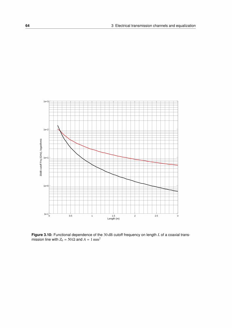
64 3 Electrical transmission channels and equalization
0 0.5 1 1.5 2 2.5 31e-1
1e+0
1e+1
1e+2
1e+3
Length (m)
30dB
cut
off F
rq (
GH
z), l
ogar
ithm
ic
Figure 3.10: Functional dependence of the 30 dB cutoff frequency on length L of a coaxial trans-mission line with Z0 = 50Ω and A = 1 mm2
3.3 Equalization techniques 65
3.3 Equalization techniques
As can be seen from the previous section, most practical transmission line topologies,especially once they grow more complex and need to span a larger distance, do not allowmultigigabit transmission without signal conditioning. This can either mean a predistortionof the signal in the transmitter, an analog filter in a receiver or even a digital feedback in thereceiver to facilitate reception of succeeding bits. It is common basis of all these approachesto remove residual ISI from the overall SBR (the time domain view), or, equivalently put, toflatten the frequency response (the frequency domain view and ultimaltey where the nameequalization stems from). Please note that the frequency responses, single bit responses andequalization results in this section already all originate from real number model simulationsof the modelling and analysis framework and the serializer system presented in chapters 4and 6.
3.3.1 Finite impulse response filter
Finite impulse response filters (in this context also called feed forward equalizers) are usedin the transmitter of a serializer. This building block uses all digital inputs ak and producesa preweighted, analog output
bk = b(kT )p(t − kT )
with the pulse function p(t) (see section 5.1) where
b(kT ) = w · a
with the so-called tap weights w. The current, preceeding and succeeding bit(s) ak formthe vector a whose weighted sum is being produced at an internal or the external node ofthe transmitter. The particular realization of weighting and summation process is of coursedependent on whether a CML or SST output or intermediate driver is used. For reasons ofpower supply rejection and the inevitable decrease in signal swing, however, virtually alldesigns in literature produce the weighted summation at their output nodes.
The concept of a four tap FIR filter is displayed in figure 3.11. This sequential shiftstructure with a single clock phase is called a full-rate architecture. It is however muchmore common to realize a multiphase design implementation strategy for the transmitterwhere the output data is produced by numerous clocks at equidistant phases. The probablymost widely adopted concept uses two clock phases (double data rate) but with rising datarates, using more clock phases has become increasingly popular over the past years [15].In this case, the FIR architecture has to be adapted accordingly. As far as the mathematicalinterpretation of the equalization process is concerned, however, the exact implementation

66 3 Electrical transmission channels and equalization
+
w-1
φ
xw0
x +
φ
w1
x +
φ w2
x +
φ
ak
bk
Figure 3.11: Conceptual view of feed forward equalization with an FIR filter
is of no importance here.
The FIR filter uses the current bit (n = 1) multiple preceeding and usually only a singlesucceeding bit to adjust the electric potential at the transmitter output. The weights wk canbe adjusted such that they optimally compensate the residual ISI of the channel SBR ifthe effect is not too strong. From a modelling point of view, the FIR filter is most easilydescribed in Z-space as a delay chain with the associated weights.
H(z) =∑
n
wnz−n (3.10)
The time discrete description of the FIR filter in z-space can, within certain limits, betranslated to a time continuous description and therefore to a frequency transfer functionvia a bilinear transformation. This process is described in more detail and in differentcontext in section 4.1. For an exemplary channel in compliance to the CEI-28-MR standard,the FIR can be shown to both remove the ISI from the SBR and to produce a much flatteroverall frequency response (see figures 3.12 and 3.13 ). As can be seen especially fromthe resulting frequency transfer function, the process of equalization at the transmitterwill equalize the signal at the expense of decreasing the overall signal to noise ratio at thetransmitter output already. Also, due to the power constraint of the transmitter∑
n
wn = 1 while necessarily w0 > wn∀n
the magnitude of correctable intersymbol interference is strictly limited.
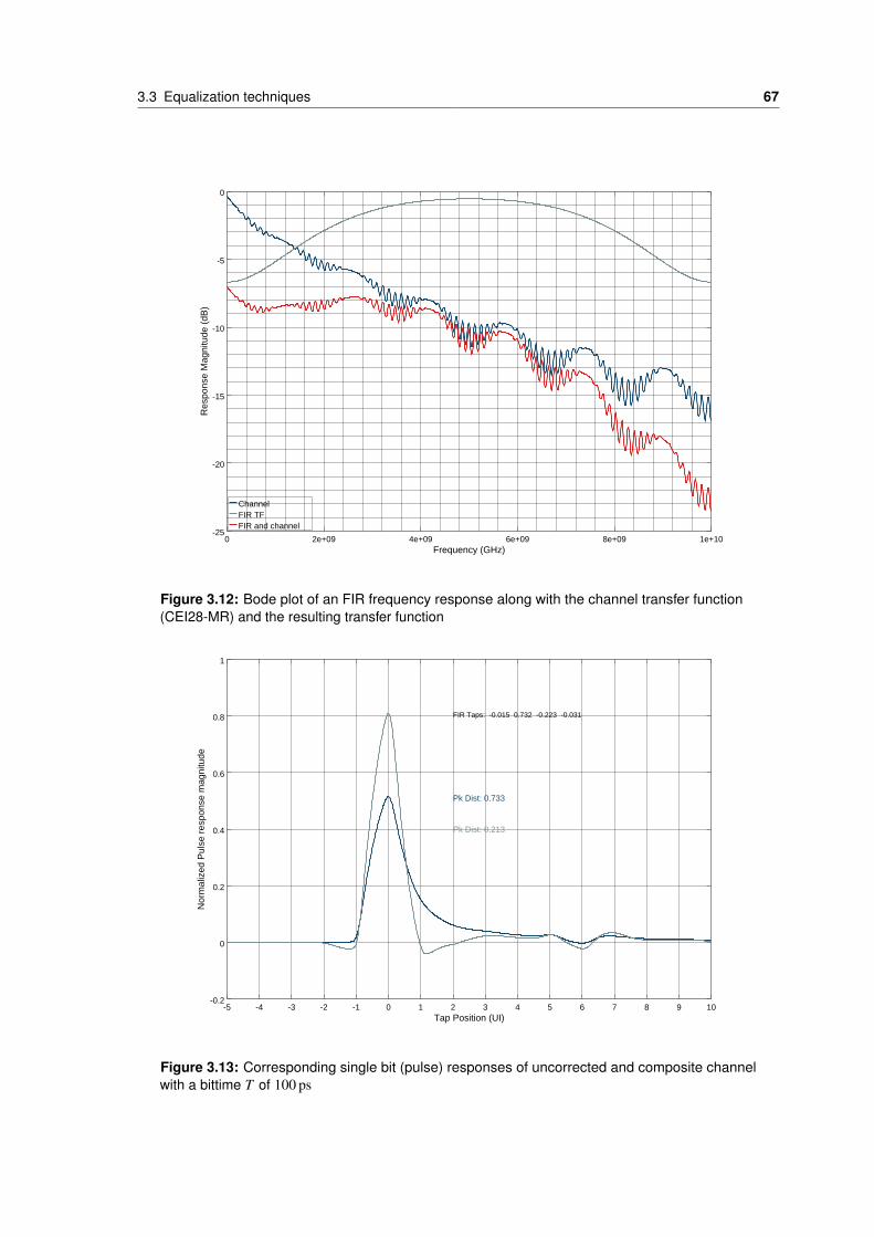
3.3 Equalization techniques 67
0 2e+09 4e+09 6e+09 8e+09 1e+10-25
-20
-15
-10
-5
0
Frequency (GHz)
Res
pons
e M
agni
tude
(dB
)
ChannelFIR TFFIR and channel
Figure 3.12: Bode plot of an FIR frequency response along with the channel transfer function(CEI28-MR) and the resulting transfer function
-5 -4 -3 -2 -1 0 1 2 3 4 5 6 7 8 9 10-0.2
0
0.2
0.4
0.6
0.8
1
Tap Position (UI)
Nor
mal
ized
Pul
se r
espo
nse
mag
nitu
de
Pk Dist: 0.733
Pk Dist: 0.213
FIR Taps: -0.015 0.732 -0.223 -0.031
Figure 3.13: Corresponding single bit (pulse) responses of uncorrected and composite channelwith a bittime T of 100 ps

68 3 Electrical transmission channels and equalization
3.3.2 Continuous time linear equalizer
The continuous time linear equalizers (CTLEs) are a means of signal preconditioning priorto analog to digital conversion in the receiver. Thus, these type of circuits are a part of theamplification chain of the receiver analog frontend. They can be implemented in eitheractive or passive ways. Since usually channel signal attenuation is sufficiently high whenequalization is required, the active structures such as the one presented in figure 3.14 aremore common as they offer additional gain and may thus reduce the number of amplifierstages and therefore noise in the signal path leading to the sampler inputs. As each gainstage in the analog receiver frontend also amplifies the noise present at its inputs, there canof course be no improvement in the signal to noise ratio as a result of equalization. Theoverall gain requirement and the resulting receiver sensitivity thus need to be carefullyanalyzed. This analysis is with respect to residual internal offsets, sampler intrinsic noiseand residual ISI.
vip(t) vin(t)
Isrc Isrc
Rd Rd
VDD
CL
von(t)
CL
vop(t)
Figure 3.14: A fully differential continuous time linear equalizer with resistive and capacitivedegeneration.
The general transfer function of an active CTLE can be derived from its small signalmodel. Ignoring the gate-drain capacitance of the input transistors Cgd and their finiteoutput impedance rds for the moment, the transfer function of the CTLE circuit shown in

3.3 Equalization techniques 69
figure 3.14 can be calculated to [9]
H(s) =(gmRD)(1 + sRsCs)
(1 + sRsCs + gmRs/2)(1 + sRDCL)
Here RS and CS are the (usually adjustable) source degeneration resistance and capacitancewhile gm is the small signal gain of the input transistors. The locations of the zero and thetwo poles of the transfer function above calculate to
ωz =1
RsCs
ωp1 =1 + gmRs/2
RsCs
and
ωp2 =1
RDCD
respectively. Figure 3.15 shows an example transfer function for a CTLE with a bandwidthof 6.8 GHz (the location of the second pole), a zero located at roughly 490 MHz and thefirst pole located at 6.54 GHz.
In order to compensate a first order low pass channel with a cutoff frequency of fBW,s
for a signal at a data rate of R (and thus T = 1/R) it can be shown that the required peak orDC gain can be calculated [9] from
Apk
ADC= 0.5 ·
fBW,pk
fBW,ch(3.11)
where fBW,pk ≈2
3T has to coincide with both fp1,p2 and fz has to be chosen to coincidewith fBW,ch . From the transfer function, the required gain levels can then be calculatedaccording to
ADC =gmRD
1 + gmRs2
and therefore
Apk = ADCωp1,p2
ωz
Apparently, there is a power tradeoff to two sides. The peak gain level will directlyincrease the power of the amplification stage itself. On the other hand, if we choose alower peak gain level, the gain in the low frequency limit (towards DC) will have to besignificantly lower to satisfy equation 3.11. However, the lower the attenuation is chosen,
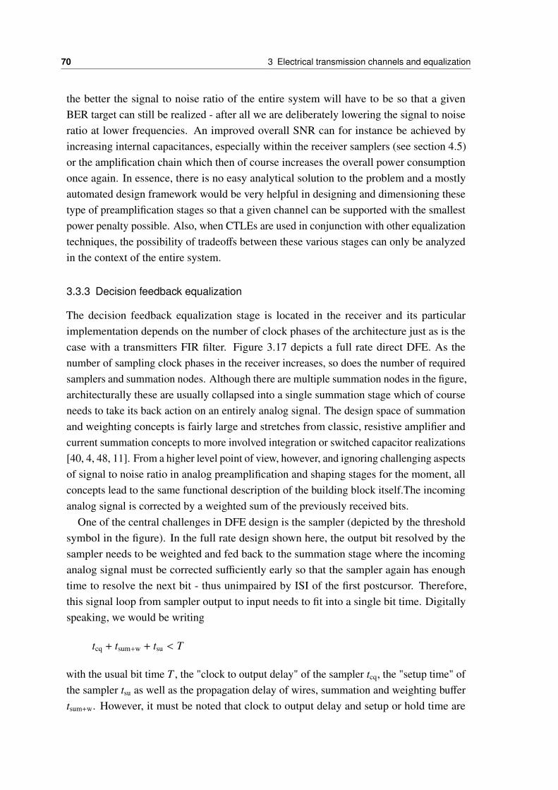
70 3 Electrical transmission channels and equalization
the better the signal to noise ratio of the entire system will have to be so that a givenBER target can still be realized - after all we are deliberately lowering the signal to noiseratio at lower frequencies. An improved overall SNR can for instance be achieved byincreasing internal capacitances, especially within the receiver samplers (see section 4.5)or the amplification chain which then of course increases the overall power consumptiononce again. In essence, there is no easy analytical solution to the problem and a mostlyautomated design framework would be very helpful in designing and dimensioning thesetype of preamplification stages so that a given channel can be supported with the smallestpower penalty possible. Also, when CTLEs are used in conjunction with other equalizationtechniques, the possibility of tradeoffs between these various stages can only be analyzedin the context of the entire system.
3.3.3 Decision feedback equalization
The decision feedback equalization stage is located in the receiver and its particularimplementation depends on the number of clock phases of the architecture just as is thecase with a transmitters FIR filter. Figure 3.17 depicts a full rate direct DFE. As thenumber of sampling clock phases in the receiver increases, so does the number of requiredsamplers and summation nodes. Although there are multiple summation nodes in the figure,architecturally these are usually collapsed into a single summation stage which of courseneeds to take its back action on an entirely analog signal. The design space of summationand weighting concepts is fairly large and stretches from classic, resistive amplifier andcurrent summation concepts to more involved integration or switched capacitor realizations[40, 4, 48, 11]. From a higher level point of view, however, and ignoring challenging aspectsof signal to noise ratio in analog preamplification and shaping stages for the moment, allconcepts lead to the same functional description of the building block itself.The incominganalog signal is corrected by a weighted sum of the previously received bits.
One of the central challenges in DFE design is the sampler (depicted by the thresholdsymbol in the figure). In the full rate design shown here, the output bit resolved by thesampler needs to be weighted and fed back to the summation stage where the incominganalog signal must be corrected sufficiently early so that the sampler again has enoughtime to resolve the next bit - thus unimpaired by ISI of the first postcursor. Therefore,this signal loop from sampler output to input needs to fit into a single bit time. Digitallyspeaking, we would be writing
tcq + tsum+w + tsu < T
with the usual bit time T , the "clock to output delay" of the sampler tcq, the "setup time" ofthe sampler tsu as well as the propagation delay of wires, summation and weighting buffertsum+w. However, it must be noted that clock to output delay and setup or hold time are
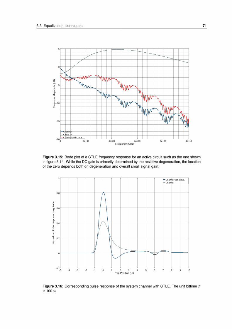
3.3 Equalization techniques 71
0 2e+09 4e+09 6e+09 8e+09 1e+10-20
-15
-10
-5
0
5
Frequency (GHz)
Res
pons
e M
agni
tude
(dB
)
ChannelCTLE TFChannel and CTLE
Figure 3.15: Bode plot of a CTLE frequency response for an active circuit such as the one shownin figure 3.14. While the DC gain is primarily determined by the resistive degeneration, the locationof the zero depends both on degeneration and overall small signal gain.
-5 -4 -3 -2 -1 0 1 2 3 4 5 6 7 8 9 10-0.2
0
0.2
0.4
0.6
0.8
1
Tap Position (UI)
Nor
mal
ized
Pul
se r
espo
nse
mag
nitu
de
Channel with CTLEChannel
Figure 3.16: Corresponding pulse response of the system channel with CTLE. The unit bittime Tis 100 ns
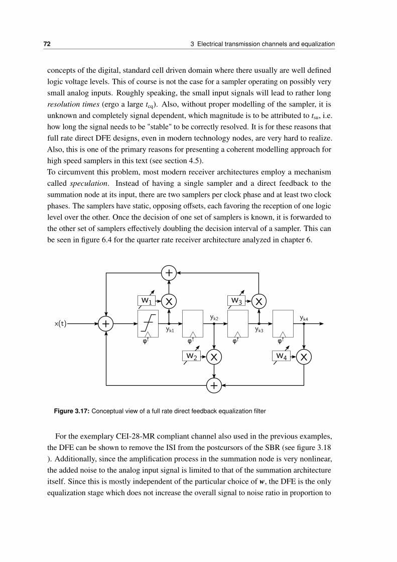
72 3 Electrical transmission channels and equalization
concepts of the digital, standard cell driven domain where there usually are well definedlogic voltage levels. This of course is not the case for a sampler operating on possibly verysmall analog inputs. Roughly speaking, the small input signals will lead to rather longresolution times (ergo a large tcq). Also, without proper modelling of the sampler, it isunknown and completely signal dependent, which magnitude is to be attributed to tsu, i.e.how long the signal needs to be "stable" to be correctly resolved. It is for these reasons thatfull rate direct DFE designs, even in modern technology nodes, are very hard to realize.Also, this is one of the primary reasons for presenting a coherent modelling approach forhigh speed samplers in this text (see section 4.5).To circumvent this problem, most modern receiver architectures employ a mechanismcalled speculation. Instead of having a single sampler and a direct feedback to thesummation node at its input, there are two samplers per clock phase and at least two clockphases. The samplers have static, opposing offsets, each favoring the reception of one logiclevel over the other. Once the decision of one set of samplers is known, it is forwarded tothe other set of samplers effectively doubling the decision interval of a sampler. This canbe seen in figure 6.4 for the quarter rate receiver architecture analyzed in chapter 6.
φ
+φ
w1 x
+
φ
x(t)yk4
φ
w3 x
w2 x
+
w4 x
yk1
yk2
yk3
Figure 3.17: Conceptual view of a full rate direct feedback equalization filter
For the exemplary CEI-28-MR compliant channel also used in the previous examples,the DFE can be shown to remove the ISI from the postcursors of the SBR (see figure 3.18). Additionally, since the amplification process in the summation node is very nonlinear,the added noise to the analog input signal is limited to that of the summation architectureitself. Since this is mostly independent of the particular choice of w, the DFE is the onlyequalization stage which does not increase the overall signal to noise ratio in proportion to
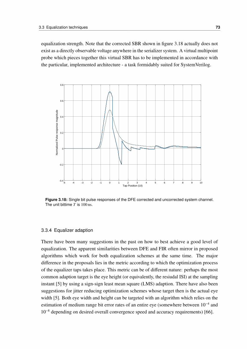
3.3 Equalization techniques 73
equalization strength. Note that the corrected SBR shown in figure 3.18 actually does notexist as a directly observable voltage anywhere in the serializer system. A virtual multipointprobe which pieces together this virtual SBR has to be implemented in accordance withthe particular, implemented architecture - a task formidably suited for SystemVerilog.
-5 -4 -3 -2 -1 0 1 2 3 4 5 6 7 8 9 10-0.4
-0.2
0
0.2
0.4
0.6
0.8
Tap Position (UI)
Nor
mal
ized
Pul
se r
espo
nse
mag
nitu
de
Figure 3.18: Single bit pulse responses of the DFE corrected and uncorrected system channel.The unit bittime T is 100 ns.
3.3.4 Equalizer adaption
There have been many suggestions in the past on how to best achieve a good level ofequalization. The apparent similarities between DFE and FIR often mirror in proposedalgorithms which work for both equalization schemes at the same time. The majordifference in the proposals lies in the metric according to which the optimization processof the equalizer taps takes place. This metric can be of different nature: perhaps the mostcommon adaption target is the eye height (or equivalently, the resiudal ISI) at the samplinginstant [5] by using a sign-sign least mean square (LMS) adaption. There have also beensuggestions for jitter reducing optimization schemes whose target then is the actual eyewidth [5]. Both eye width and height can be targeted with an algorithm which relies on theestimation of medium range bit error rates of an entire eye (somewhere between 10−4 and10−8 depending on desired overall convergence speed and accuracy requirements) [66].
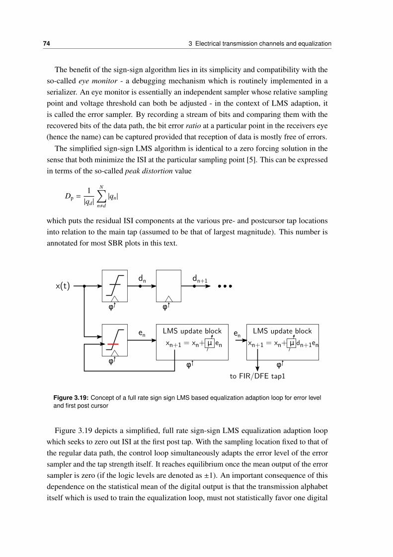
74 3 Electrical transmission channels and equalization
The benefit of the sign-sign algorithm lies in its simplicity and compatibility with theso-called eye monitor - a debugging mechanism which is routinely implemented in aserializer. An eye monitor is essentially an independent sampler whose relative samplingpoint and voltage threshold can both be adjusted - in the context of LMS adaption, itis called the error sampler. By recording a stream of bits and comparing them with therecovered bits of the data path, the bit error ratio at a particular point in the receivers eye(hence the name) can be captured provided that reception of data is mostly free of errors.
The simplified sign-sign LMS algorithm is identical to a zero forcing solution in thesense that both minimize the ISI at the particular sampling point [5]. This can be expressedin terms of the so-called peak distortion value
Dp =1|qd|
N∑n,d
|qn|
which puts the residual ISI components at the various pre- and postcursor tap locationsinto relation to the main tap (assumed to be that of largest magnitude). This number isannotated for most SBR plots in this text.
φφ
x(t)dn
φ
dn+1
en LMS update block
φ
xn+1 = xn+ μ enen LMS update block
φ
xn+1 = xn+ μ dn+1en
to FIR/DFE tap1
Figure 3.19: Concept of a full rate sign sign LMS based equalization adaption loop for error leveland first post cursor
Figure 3.19 depicts a simplified, full rate sign-sign LMS equalization adaption loopwhich seeks to zero out ISI at the first post tap. With the sampling location fixed to that ofthe regular data path, the control loop simultaneously adapts the error level of the errorsampler and the tap strength itself. It reaches equilibrium once the mean output of the errorsampler is zero (if the logic levels are denoted as ±1). An important consequence of thisdependence on the statistical mean of the digital output is that the transmission alphabetitself which is used to train the equalization loop, must not statistically favor one digital
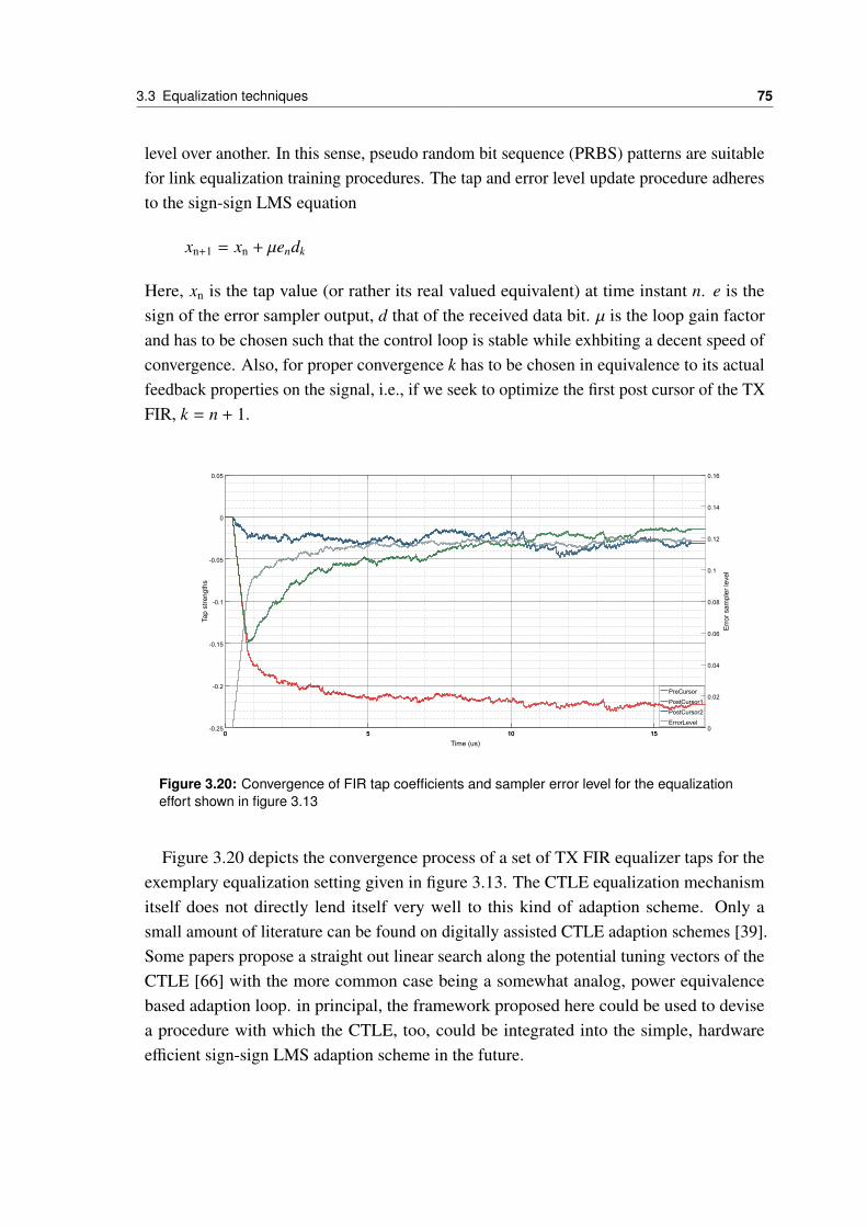
3.3 Equalization techniques 75
level over another. In this sense, pseudo random bit sequence (PRBS) patterns are suitablefor link equalization training procedures. The tap and error level update procedure adheresto the sign-sign LMS equation
xn+1 = xn + µendk
Here, xn is the tap value (or rather its real valued equivalent) at time instant n. e is thesign of the error sampler output, d that of the received data bit. µ is the loop gain factorand has to be chosen such that the control loop is stable while exhbiting a decent speed ofconvergence. Also, for proper convergence k has to be chosen in equivalence to its actualfeedback properties on the signal, i.e., if we seek to optimize the first post cursor of the TXFIR, k = n + 1.
0.16
0.14
0.12
0.1
0.08
0.06
0.04
0.02
0151050
Tap
stre
ngth
s
Time (us)
0.05
0
-0.05
-0.1
-0.15
-0.2
-0.2515
PreCursor
PostCursor1
PostCursor2
ErrorLevel
1050
Err
or s
ampl
er le
vel
Figure 3.20: Convergence of FIR tap coefficients and sampler error level for the equalizationeffort shown in figure 3.13
Figure 3.20 depicts the convergence process of a set of TX FIR equalizer taps for theexemplary equalization setting given in figure 3.13. The CTLE equalization mechanismitself does not directly lend itself very well to this kind of adaption scheme. Only asmall amount of literature can be found on digitally assisted CTLE adaption schemes [39].Some papers propose a straight out linear search along the potential tuning vectors of theCTLE [66] with the more common case being a somewhat analog, power equivalencebased adaption loop. in principal, the framework proposed here could be used to devisea procedure with which the CTLE, too, could be integrated into the simple, hardwareefficient sign-sign LMS adaption scheme in the future.
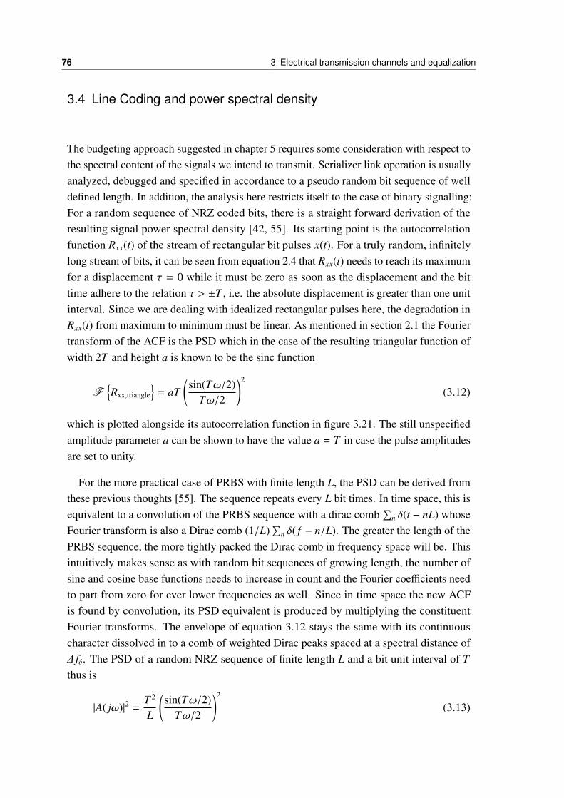
76 3 Electrical transmission channels and equalization
3.4 Line Coding and power spectral density
The budgeting approach suggested in chapter 5 requires some consideration with respect tothe spectral content of the signals we intend to transmit. Serializer link operation is usuallyanalyzed, debugged and specified in accordance to a pseudo random bit sequence of welldefined length. In addition, the analysis here restricts itself to the case of binary signalling:For a random sequence of NRZ coded bits, there is a straight forward derivation of theresulting signal power spectral density [42, 55]. Its starting point is the autocorrelationfunction Rxx(t) of the stream of rectangular bit pulses x(t). For a truly random, infinitelylong stream of bits, it can be seen from equation 2.4 that Rxx(t) needs to reach its maximumfor a displacement τ = 0 while it must be zero as soon as the displacement and the bittime adhere to the relation τ > ±T , i.e. the absolute displacement is greater than one unitinterval. Since we are dealing with idealized rectangular pulses here, the degradation inRxx(t) from maximum to minimum must be linear. As mentioned in section 2.1 the Fouriertransform of the ACF is the PSD which in the case of the resulting triangular function ofwidth 2T and height a is known to be the sinc function
FRxx,triangle
= aT
(sin(Tω/2)
Tω/2
)2
(3.12)
which is plotted alongside its autocorrelation function in figure 3.21. The still unspecifiedamplitude parameter a can be shown to have the value a = T in case the pulse amplitudesare set to unity.
For the more practical case of PRBS with finite length L, the PSD can be derived fromthese previous thoughts [55]. The sequence repeats every L bit times. In time space, this isequivalent to a convolution of the PRBS sequence with a dirac comb
∑n δ(t − nL) whose
Fourier transform is also a Dirac comb (1/L)∑
n δ( f − n/L). The greater the length of thePRBS sequence, the more tightly packed the Dirac comb in frequency space will be. Thisintuitively makes sense as with random bit sequences of growing length, the number ofsine and cosine base functions needs to increase in count and the Fourier coefficients needto part from zero for ever lower frequencies as well. Since in time space the new ACFis found by convolution, its PSD equivalent is produced by multiplying the constituentFourier transforms. The envelope of equation 3.12 stays the same with its continuouscharacter dissolved in to a comb of weighted Dirac peaks spaced at a spectral distance of∆ fδ. The PSD of a random NRZ sequence of finite length L and a bit unit interval of Tthus is
|A( jω)|2 =T 2
L
(sin(Tω/2)
Tω/2
)2
(3.13)
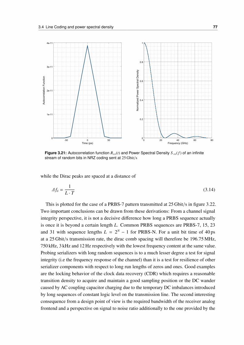
3.4 Line Coding and power spectral density 77
-50 0 500
1e-11
2e-11
3e-11
4e-11
Time (ps)
Aut
ocor
rela
tion
Fun
ctio
n
0 20 40 60 800
0.2
0.4
0.6
0.8
1
Frequency (GHz)
Nor
mal
ized
Pow
er S
pect
ral D
ensi
ty
Figure 3.21: Autocorrelation function Rxx(t) and Power Spectral Density S xx( f ) of an infinitestream of random bits in NRZ coding sent at 25 Gbit/s
while the Dirac peaks are spaced at a distance of
∆ fδ =1
L · T(3.14)
This is plotted for the case of a PRBS-7 pattern transmitted at 25 Gbit/s in figure 3.22.Two important conclusions can be drawn from these derivations: From a channel signalintegrity perspective, it is not a decisive difference how long a PRBS sequence actuallyis once it is beyond a certain length L. Common PRBS sequences are PRBS-7, 15, 23and 31 with sequence lengths L = 2N − 1 for PRBS-N. For a unit bit time of 40 psat a 25 Gbit/s transmission rate, the dirac comb spacing will therefore be 196.75 MHz,750 kHz, 3 kHz and 12 Hz respectively with the lowest frequency content at the same value.Probing serializers with long random sequences is to a much lesser degree a test for signalintegrity (i.e the frequency response of the channel) than it is a test for resilience of otherserializer components with respect to long run lengths of zeros and ones. Good examplesare the locking behavior of the clock data recovery (CDR) which requires a reasonabletransition density to acquire and maintain a good sampling position or the DC wandercaused by AC coupling capacitor charging due to the temporary DC imbalances introducedby long sequences of constant logic level on the transmission line. The second interestingconsequence from a design point of view is the required bandwidth of the receiver analogfrontend and a perspective on signal to noise ratio additionally to the one provided by the
78 3 Electrical transmission channels and equalization
eye diagram perspective (see section 2.2.1). Normalizing the PSD to unity and integratingover frequency provides the plot of figure 3.23. It shows how much of the total signalpower P is contained from DC up to a given frequency. Normalizing the x-axis to T · f ,one can see that about 80 % of the total signal power is already contained at half the signalsNyquist frequency. In order to capture about 93 % of the signal energy, an integration up toabout 3/4th of the Nyquist frequency has to be made while for 99 %, already the Nyquistfrequency has to be exceeded by a factor of 1.6. While the extension of the frequencybandwidth only leads to a very modest increase in additional signal power, the constituentcomponents of the required amplification chain (transistors, resistors) produce all whiteGaussian noise of unlimited spectral extent 1. An extension in bandwidth by a factor ofN will therefore also increase the total in-band noise by approximately the same factor.Evidently, there will be a particular point in frequency at which an additional increase inbandwidth will inevitably lead to a reduction in signal to noise ratio. However, there areother, often bandlimited sources of noise in the analog frontend of the receiver such asthe power supply induced noise which is filtered by the on-die capacitances. The requiredbandwidth can therefore often only be found approximatively and it has become commonpractice from an energy efficiency point of view to limit the bandwidth to about two thirdsof the Nyquist rate.
For narrowband systems, the so-called spot signal to noise ratio, the relation of signalpower to noise power at and in close vicinity to a certain frequency is the decisive quantity.In theses type of applications, information is modulated onto a carrier of specific frequency.These modulations can be either in amplitude, phase or both but usually are stronglylimited to a certain frequency band around the central carrier where transmission channeland noise properties of all components usually change mildly. In broadband applications,however, depending on the line coding the signal-to-noise ratio is more difficult to analyze.Of course, it is always possible to record or derive an eye diagram at the output of anygiven subcomponent in the system. However, for some design choices, the view describedabove delivers valuable insight into how subcomponents may be reasonably constrained.
There have also been publications on more advanced line coding schemes for electricalmulti-gigabit serializers. These include either the use of duobinary coding [32] or theeven more involved PAM-4 signalling scheme [32] [62] [13]. The common benefit ofboth is a compression of the PSD main lobes signal power to only half the frequencybandwidth. This comes at the expense of introducing more signalling levels and thusrequires the transmitter to produce a broader range of output voltage levels (somethingvery akin to an FIR based output) and the receiver to resolve these distinct levels back to adigital representation. In the receiver this necessitates an increased number of samplersand the additional signalling levels decrease the signal to noise ratio from the start. It
1 Unlimited at least with respect to the frequency ranges described here

3.4 Line Coding and power spectral density 79
0 5 10 15 20 250
0.2
0.4
0.6
0.8
1
Frequency (GHz)
Nor
mal
ized
Pow
er S
pect
ral D
ensi
ty
Figure 3.22: Power Spectral Density S xx( f ) of a PRBS-7 stream of bits in NRZ coding sent at25 Gbit/s
0 1 2 3 40
0.2
0.4
0.6
0.8
1
Frequency normalized to fNy
Cum
ulat
ive
spec
tral
pow
er
Figure 3.23: Cumulative power contained in an NRZ PSD normalized to the Nyquist frequency ofthe bit stream
is therefore highly dependent on data rate and the channel used, whether or not a morecomplicated signalling scheme provides an advantage with respect to reaching lower BER

80 3 Electrical transmission channels and equalization
levels. As more recent papers suggest [28] in the near future, it may therefore be a viableoption for transmitter and receivers to support more than a single line coding and rely onsophisticated analysis schemes to determine which provides the best performance within agiven environment.
4 Serializer system component modelling
This chapter will give a short introduction on the openMGT real number modelling frame-work for serializer systems and an extensive overview on its numeric backend extensionusing the open source Matlab clone Octave for advanced modelling features and post simu-lation analysis processes. It will be shown how the combined benefits of SystemVerilogreal number modelling supplemented by the flexibility and computational efficiency ofOctave can be used to model critical components. These include the transmission channel,the amplification and equalization stages in the receiver as well as the highly nonlinearreceiver sampler circuits. The resulting models will speed up the simulation processby a factor of 1000 compared to their schematic based counterparts. At the same time,unified testbenches for both model and schematic implementation will show no significantdeviation of the extracted performance metrics between the two views. These models willallow to investigate the individual influence of a broad range of subcomponent metrics orequalization choices on overall serializer system performance.
The previous chapter has highlighted the importance of a thorough understanding ofserializer system sucomponent interaction and how their respective metrics may impactdesign choices. The driving top-level metric of a cumulative bit error rate has beenshown to consider random noise effects within the components next to the various, strictlydeterministic sources of error. Additionally, it was pointed out how vastly different the timeconstants of the subcomponents are, ranging from a few MHZ for PLL/CDR bandwidthsover tens of MHz for equalization and offset cancellation calibration loops to hundredsof MHz for power distribution network induced noise all the way up to the range of GHzfor channel cutoff frequencies and intrinsic noise source bandwidths. Also, a good BERestimate cannot be obtained without properly considering the extents of and tradeoffsbetween the various equalization schemes and their different impact on signal to noiseratio. Thus, a multitude of fairly lengthy simulations have to be carried out which, due tothe inevitable fast transients, will have to use fine grained time steps. This, of course, is farfrom being a perfect fit for SPICE based simulations.
As also previously pointed out, without fast simulation models interactions of subcom-ponent metrics with higher level performance targets may be difficult to capture in transientsimulation which makes proper design space analysis at the higher layers an increasinglydifficult task. Most often, high model speedup is a result of choosing a different level ofabstraction. This level of abstraction needs to be chosen carefully and potentially even
81

82 4 Serializer system component modelling
numerous times for various models of the same component to arrive at the best solutionfor the given analysis scope. A more abstract, cumulative scope such as the CDR jitterrejection requires bare simulation performance and may thus rely on linearized modelswhich may in turn be derived from their more detailed counterparts. For smaller, moresimplistic scopes, such as the frequency response of an amplifier, the runtime of an ACsimulation alone for instance, does not justify an additional component model. Its transientresponse or its digital tuneability may, however, benefit from an abstraction of its transistorrepresentation since the real number based model view can be used to introduce a newabstraction layer directly into the general design flow. Next to a speedup, this also ensuresconsistency between the different representations and modeling approaches of all thevarious subcomponents (see again section 4.2 ).
For performance reasons, the additional modeling layers should only mimic the mostimportant properties of the physical component or, as mentioned, feature multiple levelsof abstraction depending on the higher level simulation task. An obvious example forthis is the line coding with its spectral impact on data transmission and thus intersymbolinterference which directly benefits from a more abstract modelling approach of channeland amplifier chain by real number models (see below). A less obvious analysis questionwhich can be answered more effectively with the right model abstraction is the impact ofdata coding on system functionality. The maximum run length of subsequent bits in thedata code may disturb the equilibrium state of the CDR (i.e. the recovered sampling point)since a CDR tracks transitions in the data stream.
There is a wealth of tools available to tackle different modelling and simulation tasksduring serializer design apart from schematic based design entry and all-electrical sim-ulation (SPICE, SPECTRE and many more). These include statistical simulation toolssuch as SeaSim and StatEye or microwave engineering tools such as ADS for electricalchannel analysis and characterisation for instance. These tools require a substantial amountof input parameters such as the transmitter voltage swings, rise and fall times, channelgeometry as well as the equalization properties of the receiver or models extracted fromalready conceived designs (such as IBIS models). Also, a lot of ECAD tools for integratedcircuit design provide Matlab integration to allow more complex, numerical modellingand even cosimulation where parts of the design are true schematic level while others aresignal flow models (such as those defined by Simulink). This can used for a high level ofabstraction and mathematically advanced simulation (testbench) output checks.
The major problem, however, is to keep all the subcomponent definitions and modellayers coherent with the implementation itself. A good example for this is the linear phasemodel of a CDR (see section 2.2.6) which by itself requires a substantial set of parametersto allow computation of its loop bandwidth. Knowing the bandwidth alone may already begood enough to generate an approximate statistical eye with random jitter contributionsas it may be recovered by the given receiver design. Creating the CDR subcomponents
83
such that they actually adhere to the very same constraints requires keeping all definitionsand testbenches across different programs consistent. This, of course, is a major source oferror.
There is a well established flow for defining testbenches and creating designs in thedigital hardware semicustom design flow. This flow, however, profits from a completephysical abstraction by using so-called standard cell libraries and the large signal tonoise requirements that are enforced by these (logic cell) definitions. The abstractionrequirements for analog and mixed signal systems are, however, much less generic. Also,modelling can take place at various different levels of abstraction:
The goal of VerilogA for instance is to allow a much more mathematical definitionof the relation between currents and voltages between two ports of a component - apowerful mechanism that easily allows to define completely discontinuous models forwhich convergence in DC or transient simulations may not even be achieved. VerilogAmodels run in the context of the analog simulator itself and thus produce results continuousin time and value 1.
In extension to this, VerilogA/MS was conceived which brought together the time andvalue discrete nature of Verilog HDL with the analog view of VerilogA. The languageextension for instance allows to create components with both digital and electrical portsand defines translation procedures from one domain to the other. These include filter andtransition functions to avoid grave discontinuities in analog signals as well as thresholdand cross functions which are capable of creating digital events. The simulation processis basically split into two distinct parts, the analog kernel as mentioned above and thedigital kernel with its event driven, time slot based simulation approach. The physicalquantities of voltage and current with interaction between the two (i.e. impedance) canstill be represented while the computationally efficient time discretized view can be usedwherever the digital realm is required.
Finally, there is a further step towards stronger computational simplification in Verilo-gA/MS and SystemVerilog - a grammatically more powerful successor to Verilog/A/MS. Itis called real number modelling. The time discrete nature of Verilog is ammended by a nettype of continuous real number values - the wreal net and its register-like counterpart ofreal (double) values. This mechanism allows the value and time continuous description asneeded and produced by analog environments to be translated to a value continuous buttime discrete representation. It therefore replaces the time consuming approach of variablestep size and iterative convergence processes in full analog simulation with a signal flowview as used in numeric simulators such as Matlabs SimuLink extension. There are alsoso-called user defined nettypes which allow to bundle numerous values into a user defined
1 There are of couse the usual minimal real value discretization of computer systems and the unavoidable but dynamicsimulation steps of every analog simulator
84 4 Serializer system component modelling
structure and assign a net type to them. A net-coercion mechanism which resolves whetheror not two ports of potentially different type can be interfaced with a connection modulefacilitates the use of this approach. Moreover, there are resolution functions which allow todefine custom mechanisms of resolving a multi-driver, multi-receiver situation on a giveninterconnect of the design hierarchy. The combination of these mechanisms thus allowsto mathematically mimic complicated analog interdependencies on a time discrete basiswithout having to resort to explicitly solving Kirchhoff equations of a larger network. Formore detailed information, the reader is referred to the SystemVerilog documentation [1].
For every subcomponent in the serializer system, the challenge lies in finding an appro-priate level of abstraction that exploits both the continuous character of the real numberdomain and the discretized character in the time domain to realize a model of high perfor-mance and reasonable accuracy. Subsection 4.1 will give an overview on how this can bedone in the context of SystemVerilog with signal flow models for almost generic analogfilters and describes the limitations of this process. SystemVerilogs original purpose was toimprove and automate simulation capabilities and provide stimuli of greater variability todigital designs under test. Its long term goal is to establish similar verification procedures inthe mixed signal and analog domain. The benefit of keeping the modelling procedure closeto the implementation by using the same language for testing, modelling (and in the digitalcontext even describing) a component lies in the consistency not only between modeland implementation but also between the various modelling views of a subcomponent.Model views then can have various degrees of abstraction depending on the high levelmetric to be analyzed. If feasible, the development of the model and the testbench aredone concurrently. The testbench is designed such that it can be used for extracting therelevant subdesign metrics. The common SystemVerilog based formulation (and someextensions of VerilogAMS and the simulators) makes the testbenches reusable for realnumber, electrical and possibly purely functional models alike. Therefore, the testbenchand the real number model are verified against one another. The testbench checks a designunder test with an explicitly given parameter. The model needs to use this parameter toproduce the expected reactions to the stimuli. The testbench then has to retrieve the givenmetric magnitude with the specified test procedure. In this way, the model is shown toserve both as a means of representing the implementation during design exploration andas a basis for component verification after design and before tapeout. The frameworkpresented in section 4.2 relies on these ideas to model and implement a parameterizableserializer with a top-down, digital first methodology. This was conceived in collaborationwith another dissertation. The so-called openMGT framework is briefly described here fororientation. For more details the reader is referred to [38].
Some models of a serializer system, most notably the transmission channel, requiremore computational power than almost all other elements in the design combined. Incase of channel and sampler modelling as presented in sections 4.4 and 4.5, convolution
4.1 General Real Number Modelling Considerations 85
requires multiplication of long real number vectors. This is not supported efficiently inSystemVerilog and the problem is magnified by the (current) absence of multiprocessingcapability in contemporary SystemVerilog simulators. Furthermore, a strict separationof random and deterministic effects due to simulation time optimization and problemcomplexity is one of the key design principles of the openMGT framework. Interoperationwith statistical budgeting algorithms and postprocessing of data as discussed in chapter5 requires SystemVerilog to be extended by a numeric engine. MATLAB offers suchcapabilites and, as mentioned above, commercial CAD tools offer API bridges to theseapplications. However, these are often implemented with interprocess communicationcalls and are thus enforcing a context switch within the CPU. For frequent operations suchas the convolution of a signal with a channel impulse response in a transient simulation,the communication overhead plays a vital role and needs to be diminished in importancecompared to the computation effort of convolution itself.
Fortunately, the SystemVerilog standard defines a direct programming interface (DPI)extensions which allows to extend the simulator binary with custom C code. This willpave the way of extending SystemVerilog with the powerful open source MATLAB cloneOctave. It leverages the openMGT C modelling extension (OCM) discussed in section4.3 which will be used to model channel and sampler instances efficiently with SIMDinstructions and threaded execution. It is also the gateway to the more complicated,statistical post processing which will be required by lane budgeting and peak distortionanalysis as described in chapter 5 and also provides a consistent view on composite,linearized models such as the PLL or CDR.
4.1 General Real Number Modelling Considerations
While simulator time steps in SPICE may vary in size, they are fixed with RNM simulations.SPICE offers the option of fixing the step size but this comes at a severe performanceimpact. The convergence algorithm for solving the Kirchhoff equations has to be run forevery time step of an analog simulation. When there only seems to be little change involtages or currents in the vicinity of a particular node, the simulator chooses wider timesteps if they are not constrained by the user.
The simulation speedup of real number modeling primarily lies in the abstraction ofelectrical components with a signal flow view. Thus, the time consuming process of solvingthe Kirchhoff equations for an entire, potentially huge matrix with nonlinear elements usinga successive approximation technique and variable time steps can be circumvented. In itsstead, the models have a fixed time step which needs to be chosen once for a particularsubcomponent or even the design itself (the simulation time step). Also, a single net(connection between any two ports) has only one non-interacting quantity associated with it(a real number or a logic level) to which multiple drivers (outputs) may make contributions
86 4 Serializer system component modelling
(via the resolution functions mentioned above) and multiple receivers (inputs) may sensethe value. Thus, there is no concept of impedance, wire load or wave reflection initiallyconveyed in this picture. On the other hand, newer versions of SystemVerilog offer thepossibility of creating user defined net types which allow to associate a tuple of real numberand logic values with a net. A resolution function may then be used to define, in which waymultiple drivers interact on a given value. The most basic example would be a cumulativesum of all output drivers to a net for instance. With its help, various current sourcessumming up on a single node can easily be modeled. The associated voltage drop increaseacross an attached output resistance however cannot be described without extensions toeither the resolution function of the connection or the resistor model itself.
Since the RNM approach lends itself best to signal flow descriptions of systems, theeffects of a linear, time invariant system on a signal are best described in the frequencydomain (s- space) and converted to z-space for time discretization. Then, the resulting FIRor IIR filter can be described with a few lines of code. The conversion from s- to z-spacerequires a transformation which in this case is chosen to be the bilinear transformation. Itis defined as
s =2T·
z − 1z + 1
(4.1)
with its inverse being
z =1 + T s/21 − T s/2
(4.2)
Here, T = 1fs
is the sampling rate of the time discrete system. The bilinear transformationbasically maps all elements of the s-plane s = σ+ jΩ to unit circles in the z-plane z = Ae jω.Since σ in s-space is used to enforce convergence of the transformation integrals even forunstable systems, we can safely set σ = 0 as the subcomponents described here are alleither passive or strongly bandwidth limited systems. In the z-plane, everything is thenmapped to the unit circle z = e jω.
From equation 4.2 we thus have
jΩ = s =2T
e jω − 1e jω + 1
=2T
2e− jω/2 j sin(ω/2)2e− jω/2 j cos(ω/2)
=2 jT
tan(ω
2
)(4.3)
Digital simulators in principle allow us to choose the sampling rate and simulation time stepfreely (or at least down to 1 fs which is far smaller than required by the radio frequencyand microwave regions described here). Increasing the time step, however, naturallycomes at the expense of increased simulation time and will therefore be especially hurtfulfor the purpose of simulating systems with a large spread in their characteristic timeconstants. Equation 4.3 can therefore be used to calculate the minimum time resolution
4.1 General Real Number Modelling Considerations 87
required to model a system up to a particular frequency without the nonlinearity necessarilyintroduced by the bilinear transformation process. The question which needs to be answeredbeforehand is how to select the frequency range of interest for a particular subcomponentor even the entire system. A distinct and viable choice here would be the 3 dB-cutofffrequency of the system (see section 3.4) as frequencies beyond this point provide verylimited contribution to the overall signal seen at the receiver samplers - at least if thechannels indeed have high loss characteristics as is the case in backplane and long-haulapplications.
Assuming a target angular frequency of Ω0, further simplification and rearrangement ofequation 4.3 gives
Ω0T2= tan
(ω0
2
)The approximation of tan(δ) ≈ δ holds to within 0.34 % error for δ ≤ 0.1 and to within10 % for just about δ ≤ 0.52. Thus for a stringent linear mapping between the two spaces,the general requirement
T =1
10 f0(4.4)
should be fulfilled and for a more relaxed mapping the requirement
T =1
2 f0(4.5)
is sufficient. For a system whose most wideband component features a cutoff frequency of20 GHz for instance, the simulator time steps and sampling rate of the time discrete filterrepresenting the continuous transfer function would need to be set to 5 ps for the stringentcase or 25 ps for a more relaxed setting.
Conversely, if there is a time-discrete component in the system and we are interestedin its continuous frequency response, the frequency mapping process is mediated by theatan(δ) function whose linearity is even slightly better ( 10 % for just about δ ≤ 0.6). Thismakes the mapping process reasonably linear up to frequencies of about
f0 =1
1.66T(4.6)
The time continuous frequency response estimation of an FIR filter with a data rate of10 Gbps (i.e. T = 100 ps), would therefore be only accurate up to 6 GHz which is slightlyabove half the Nyquist frequency of the given system.
For modelling analog system subcomponents with an linear time invariant (LTI) response
88 4 Serializer system component modelling
in signal flow view, an adjustable and versatile approach to translate the response of arather generic time continuous filter is required. Since for the majority of purposes in aserializer system, the number of zeros and poles up to twice the Nyquist rate is limited toonly a few, the transfer function
H(s) = A0
(1 + s
ωz0
) (1 + s
ωz1
)(1 + s
ωp0
) (1 + s
ωp1
) (1 + s
ωp2
) (4.7)
in canonical form is chosen as a starting point. Here, the set of ωz,n describe the zerosin the system while the set of ωp,n describes the poles. A0 is the DC gain of the filter. Inorder to acquire a closed form solution for the z-space filter the bilinear transformation(equation 4.2) can directly be used to replace all occurences of s in equation 4.7. Given theappropriate sampling rate (and thus frequency of clock φ in the delay elements of figure4.1), the time discrete counterpart of the time continuous transfer function can be derivedto
G(z) = A0Azn0 + n1z−1 + n2z−2 + n3z−3
1 + d1z−1 + d2z−2 + d3z−3 (4.8)
Equation 4.8 can directly be translated into SystemVerilog code by virtue of the so-calledtype II filter structure [10].
Figure 4.1 shows the generic type II time discrete filter in which a time and valuecontinuous system with gain, such as an amplifier or a passive, lumped element filter can beconverted to. In SystemVerilog, the filter weights could be implemented as fixed, numericparameters which would then need to be known at compile time of the module. However,there are serializer subcomponents, most notably the CTLE or the VGA, which requireadjustability of their transfer functions during runtime. The filter weights must therefore bedynamic values (real values/registers) rather than fixed parameters. Therefore, a numericor analytic translation between the pole/zero representation of the time continuous viewto the parameter set of the time discrete manifestation needs to be realized. While anumeric translation is indeed possible, SystemVerilog would not be the native languageto implement this process - after all, its design intent is not the formulation of rathercomplex numeric transformation processes. As described in section 4.3, however, theopenMGT extension to the opensource MATLAB clone Octave along with Octaves signalpackage1 could potentially be used here to even translate time continuous functions ofalmost arbitrary complexity to their digital counterparts. For reasons of simplicity and dueto the abovementioned limitation to only a few poles and zeros of interest, the approach
1 A package is an extension to the core functions of the numeric CAD program Octave. The signal package implementsfunctions to define and analyze both functions of time discrete and time continuous realm and also allows to translatebetween them.
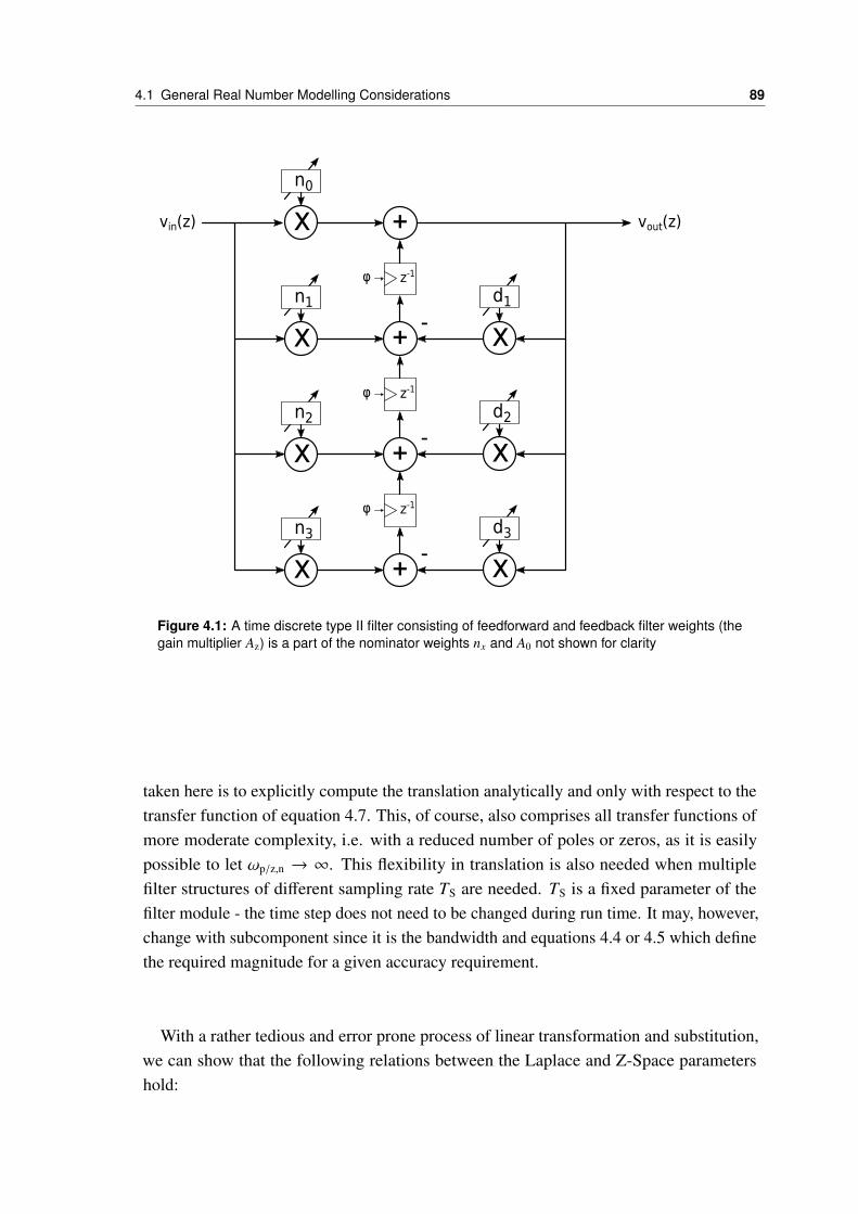
4.1 General Real Number Modelling Considerations 89
+
n0
xvin(z)
φ
n1
x
z-1
+
d1
x
φ
n2
x
z-1
+
d2
x
vout(z)
φ
n3
x
z-1
+
d3
x-
-
-
Figure 4.1: A time discrete type II filter consisting of feedforward and feedback filter weights (thegain multiplier Az) is a part of the nominator weights nx and A0 not shown for clarity
taken here is to explicitly compute the translation analytically and only with respect to thetransfer function of equation 4.7. This, of course, also comprises all transfer functions ofmore moderate complexity, i.e. with a reduced number of poles or zeros, as it is easilypossible to let ωp/z,n → ∞. This flexibility in translation is also needed when multiplefilter structures of different sampling rate TS are needed. TS is a fixed parameter of thefilter module - the time step does not need to be changed during run time. It may, however,change with subcomponent since it is the bandwidth and equations 4.4 or 4.5 which definethe required magnitude for a given accuracy requirement.
With a rather tedious and error prone process of linear transformation and substitution,we can show that the following relations between the Laplace and Z-Space parametershold:
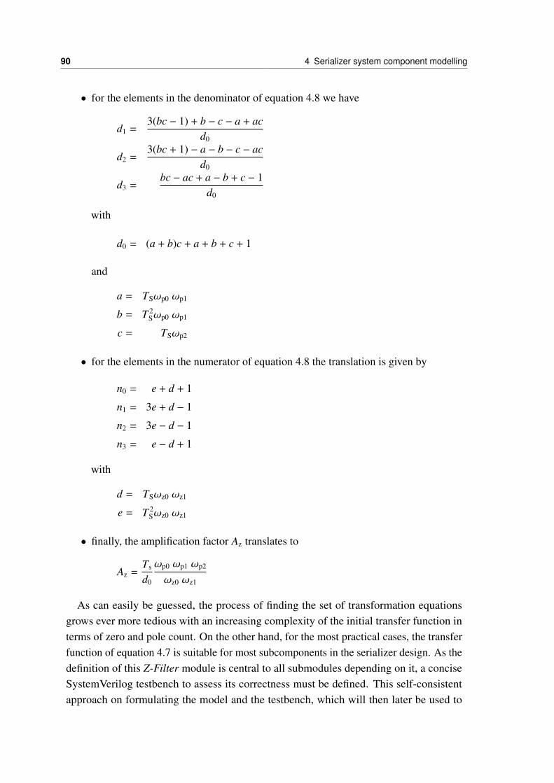
90 4 Serializer system component modelling
• for the elements in the denominator of equation 4.8 we have
d1 =3(bc − 1) + b − c − a + ac
d0
d2 =3(bc + 1) − a − b − c − ac
d0
d3 =bc − ac + a − b + c − 1
d0
with
d0 = (a + b)c + a + b + c + 1
and
a = TSωp0 ωp1
b = T 2Sωp0 ωp1
c = TSωp2
• for the elements in the numerator of equation 4.8 the translation is given by
n0 = e + d + 1
n1 = 3e + d − 1
n2 = 3e − d − 1
n3 = e − d + 1
with
d = TSωz0 ωz1
e = T 2Sωz0 ωz1
• finally, the amplification factor Az translates to
Az =Ts
d0
ωp0 ωp1 ωp2
ωz0 ωz1
As can easily be guessed, the process of finding the set of transformation equationsgrows ever more tedious with an increasing complexity of the initial transfer function interms of zero and pole count. On the other hand, for the most practical cases, the transferfunction of equation 4.7 is suitable for most subcomponents in the serializer design. As thedefinition of this Z-Filter module is central to all submodules depending on it, a conciseSystemVerilog testbench to assess its correctness must be defined. This self-consistentapproach on formulating the model and the testbench, which will then later be used to
4.2 The openMGT framework 91
verify the actual implementation against the model, relies on the openMGT and the OCMframework. We will therefore pick up the thread we started here in the next two sections.
4.2 The openMGT framework
Implementation
Specifications + MetricsParameters and Ports/Signals
TestbenchesMonitors, Scoreboard, Coverages, Assertions
Models(Leaf Cells)
Behavioral HDL / System Verilog
Behavioral Interface
Wreal Interface
Electrical / Analog Interface
MostlyCommon SystemVerilog CodeBase
Real Number Model (Power Aware)
VerilogA Model(i.e. impedance and noise)
SynthesizableHDL
Structural HDL(Hierarchy)
Gate LevelNetlist
Schematics with fixed parameters
Leaf CellHDL module(placeholder)
Placed/Routed Macro Transistor level
Drives definition of Ascertains complianceAscertains compliance / Checks against modelDerives submodule parameters and definesCustom Scripts / Tools of digital methodologyTraditional, manual implementation
MacroGDS with Lib/LEF
Final Macro / GDS
Figure 4.2: Overview of the openMGT framework
Figure 4.2 presents an overview of the openMGT framework. The framework is centeredaround the idea of simultaneous conception of testbenches, models and general designstructure as a hierarchy of subdesigns (components or cells, we will use these termsinterchangeably). The development process is a top-down specification and metric drivenflow. Specifications are well-defined, observable (hence testbench checkable) quantitiesof design performance. For a serializer, they would for instance be given by the I/Ostandard specification. Metrics are essentially the same, apart from the abscence of ahigher level constraint to them. Instead the constraint to a metric may originate fromanother performance metric or is imposed on a design by subcomponents of the samehierarchy. The common mode of a differential amplifier not interfacing with the outsideworld of the overall design is a good example for a such a metric. The major difference
92 4 Serializer system component modelling
between specification and metric therefore lies in the fact that metrics of one componentmay be traded off against those of another to realize a certain, higher level design metric oreventually specification. In the context of a network communication link, if we are free todefine our own protocol stack and there is no standard to adhere to, the distinction betweenspecification and metric would evidently be obsolete. In the following, we will thereforecarry on with the term metric exclusively.
Metrics are often associated with one or two distinct ports of a component or thecomponent itself. In addition and close relation to digital designs, components haveparameters such that they may occur within a design hierarchy numerous times, possiblywith a different parameter set for every so-called instance. In larger hierarchies, oftentimesthe implementation of a subcomponent itself is just an arrangement of more specificsubcomponents. In openMGT, these cells are dubbed structural as they can be described asa pure relation of subcomponents. This is done in ordinary Verilog HDL language. Whilefor digital designs, these ’quantized’ notions come about naturally, there is only a subsetof typical analog components that is suitable for the same kind of treatment. Nevertheless,especially in mixed signal designs with a decent number of DAC and ADC based controlloops, the automated procedures of defining vectors and arrays of instances simplifythe description of a system compared to a schematic (i.e. graphical) view substantially.Moreover, the well established netlisting routines of HDL to gate-level compilers can beused to automatically generate large schematics, symbols and schematic templates - amechanism that can be used to enforce consistency between modelling and implementationview [38]. A strict separation of digital and analog realms is an essential part of theworkflow. This is because the digital subcomponents will and shall of course profit fromthe well-established industry semicustom implementation flow. Analog components on theother hand are so-called leaf cells, a special kind of structural cell. The leaf cells definethe interface and parameters of the given subcomponent and serve as a placeholder for theparticular model to be used.
4.2.1 Leaf cells
Leaf cells may then contain one of the model views as required by a particular (higherlevel) testbench or the actual schematic implementation itself. The translation processbetween the text based Verilog description and the graphics based schematic representationis performed by a custom scripting process (for details see [38]). This ensures consistencybetween the structural description and the schematic implementation of the leaf cell. Asevident from the foregoing discussion, in order to model and test a particular metric themodel scope has to be chosen appropriately. The various model scopes are defined in thefollowing and presented in conjunction with a small example of how the scope may be ofuse in a larger design context:
4.2 The openMGT framework 93
Behavioral HDL Behavioral HDL relies on all constructs provided by the particular HDLlanguage. For openMGT, the HDL used is Verilog. Since leaf cells are never going tobe used in the semi-custom design flow, the full spectrum of language constructs can beemployed without adhering to best coding principles for synthesizability. Care must betaken however to define HDL which simulates efficiently. Especially the number of eventsgenerated by the model and the number of constructs sensitive to events needs to be keptsmall for good simulation performance. Considering an amplifier within a larger designcontext, its main purpose from a behavioral point of view is to pass on a signal from theinput to its output. Behavioral HDL, in addition to being discrete in time, only supportsdigital levels, the high impedance state and an error state x for a given signal/port. Wecan thus model some details of quite general behavior with respect to amplifier operatingconditions. These include for instance the proper reaction to the presence or abscenceof ground and power supplies or reference voltages and currents. A differential NMOSCML amplifier stage for instance might pull both of its inputs to supply potential whenthe reference voltage for its tail current source is grounded. Behavioral HDL thereforepossesses its major strength in checking proper interconnectivity, its comfortable way ofdefining more complicated component interfaces (with tuning and calibration vectors forinstance) and in asserting the correctness of the general signal flow in the design (i.e. thatthe output of an amplifier chain is not inverted).
Real number model As mentioned above, with real number models the concepts arelimited to a signal flow description or, in case of user defined net types and resolutionfunctions, to slightly more complicated arrangements such as some basic Kirchhoff con-servation type calculations 1. On the other hand, it is the level of abstraction that bringswith it the fundamental speed-up required to solve more complicated analysis tasks ofsystems with large time constant spreads or to simulate designs of larger scope. Eventhough the signal flow view is not much different from that of the behavioral description,the availability of virtually value continuous net and register types allows to implementsome very important aspects of system subcomponents. In the context of the amplifierexample, it is now for instance possible to check input common mode levels, define outputcommon mode levels, signal swings and, by virtue of the Z-Filter module described insection 4.1, even transfer function properties. With the poles and zeros even being ad-justable, the central functions of linear equalization and variable gain adjustment can bedescribed and parametrically constrained already at this fairly abstract level. It must ofcourse be understood that there may be some reiterations needed once the actual designof a component is known. This can either mean an adjustment in metric values or the
1 An example would be the summation of currents on one real number structural component while tracking impedanceor voltage on another, for well constrained circuit topologies, the problem can often be simplified in this manner
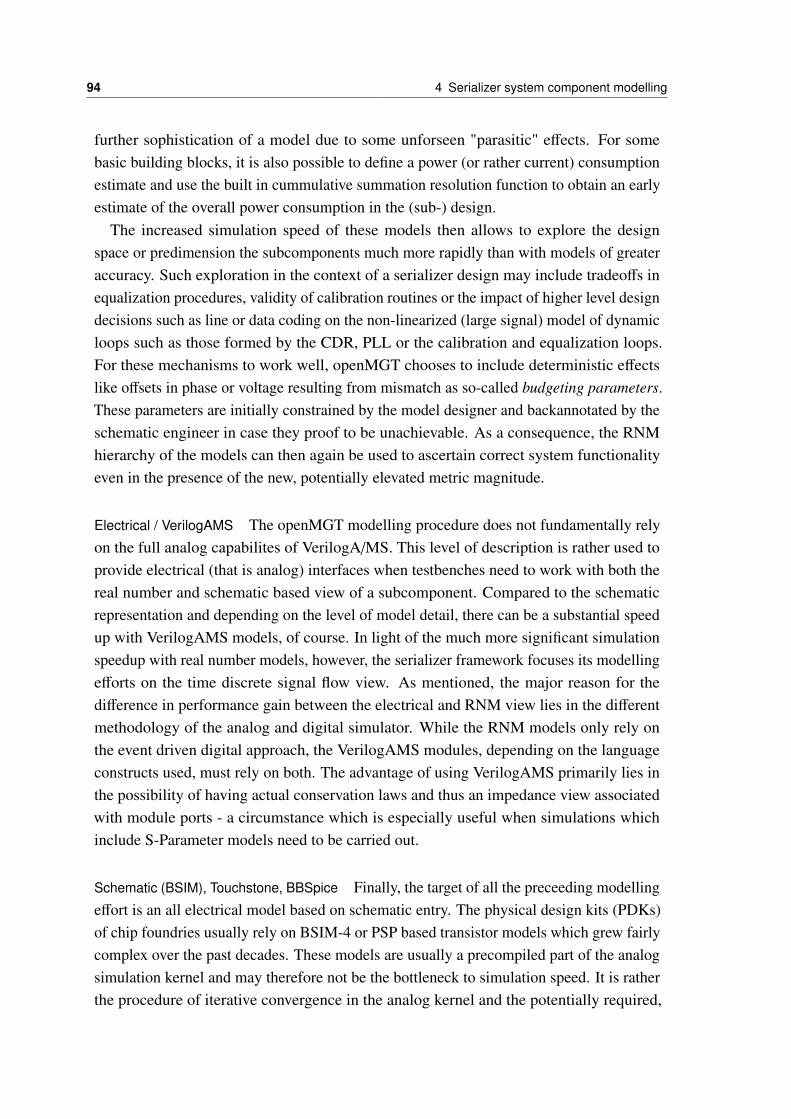
94 4 Serializer system component modelling
further sophistication of a model due to some unforseen "parasitic" effects. For somebasic building blocks, it is also possible to define a power (or rather current) consumptionestimate and use the built in cummulative summation resolution function to obtain an earlyestimate of the overall power consumption in the (sub-) design.
The increased simulation speed of these models then allows to explore the designspace or predimension the subcomponents much more rapidly than with models of greateraccuracy. Such exploration in the context of a serializer design may include tradeoffs inequalization procedures, validity of calibration routines or the impact of higher level designdecisions such as line or data coding on the non-linearized (large signal) model of dynamicloops such as those formed by the CDR, PLL or the calibration and equalization loops.For these mechanisms to work well, openMGT chooses to include deterministic effectslike offsets in phase or voltage resulting from mismatch as so-called budgeting parameters.These parameters are initially constrained by the model designer and backannotated by theschematic engineer in case they proof to be unachievable. As a consequence, the RNMhierarchy of the models can then again be used to ascertain correct system functionalityeven in the presence of the new, potentially elevated metric magnitude.
Electrical / VerilogAMS The openMGT modelling procedure does not fundamentally relyon the full analog capabilites of VerilogA/MS. This level of description is rather used toprovide electrical (that is analog) interfaces when testbenches need to work with both thereal number and schematic based view of a subcomponent. Compared to the schematicrepresentation and depending on the level of model detail, there can be a substantial speedup with VerilogAMS models, of course. In light of the much more significant simulationspeedup with real number models, however, the serializer framework focuses its modellingefforts on the time discrete signal flow view. As mentioned, the major reason for thedifference in performance gain between the electrical and RNM view lies in the differentmethodology of the analog and digital simulator. While the RNM models only rely onthe event driven digital approach, the VerilogAMS modules, depending on the languageconstructs used, must rely on both. The advantage of using VerilogAMS primarily lies inthe possibility of having actual conservation laws and thus an impedance view associatedwith module ports - a circumstance which is especially useful when simulations whichinclude S-Parameter models need to be carried out.
Schematic (BSIM), Touchstone, BBSpice Finally, the target of all the preceeding modellingeffort is an all electrical model based on schematic entry. The physical design kits (PDKs)of chip foundries usually rely on BSIM-4 or PSP based transistor models which grew fairlycomplex over the past decades. These models are usually a precompiled part of the analogsimulation kernel and may therefore not be the bottleneck to simulation speed. It is ratherthe procedure of iterative convergence in the analog kernel and the potentially required,
4.3 The openMGT C and Octave modelling extension (OCM) 95
very small time steps chosen by the simulator whenever fast transients are encounteredthat lead to longer simulation times as a design grows in complexity. Therefore, whilesimulation accuracy of this layer is by far the greatest, its speed can be very low.
4.2.2 Testbenches
Wherever applicable the ports of a subcomponent or the subcomponent itself are associatedwith constrained metrics and the testbenches are conceived such that these constraintsare captured by the testbench and satisfied by both model and implementation. TheSystemVerilog extensions of recent years [1] enables this process by allowing the definitionof the same testbench with multiple different levels of abstraction and the VerilogAMSlanguage allows for the translation process between real number, behavioral and electricalmodelling domains. The possibility to reuse a large portion of a common code basetherefore decreases the probability of inconsistensies in how metrics are defined or probed.There are of course some limitations to this process wherever models cannot fully capturethe analog reality of subcomponents, a circumstance most common as soon as impedancedependent effects come into play. Such would for instance be the case for models ofoperational amplifiers in feedback configuration whose loop stability explicitly depends onthe output loading condition for instance. A testbench for the exemplary amplifier in thisdiscussion can for instance be designed to probe and extract the pole and zero locations ofits transfer function in the loaded condition (i.e. in the electrical case with input and outputimpedances considered). The procedure of how this can be done is discussed in the nextsection where the openMGT C/Octave modelling framework extension is outlined.
4.3 The openMGT C and Octave modelling extension (OCM)
One of the major design guidelines of the openMGT framework lies in the strict separationof deterministic and random contributions to overall system behavior. As explained, thestatistical nature of random processes makes it very unlikely to capture all the importantworst case conditions within a transient simulation run, especially for systems with verylow bit error rate targets. Therefore, treatment of random noise contributions in voltageand phase is delegated to the OCM numeric post processing environment which alsohandles the linearization and calculation of the CDR closed loop transfer function andthe impact of sampler nonidealities on the data captured by the receiver. Also, once themodelling process is complete or the schematic design of the serializer system is fullyavailable, the entire design has to be simulated in concert with the physical target channels.While this task is natively handeled for schematic based designs in conjunction with S-Parameter based channels, the real number model layer performance would severely sufferfrom being cosimulated with a file based channel model. File based channel models are
96 4 Serializer system component modelling
always simulated within the analog simulator when interfaced to RNM subcomponents viaVerilogAMS connect modules. However, all negative consequences of invoking the analogsimulator will then again be unavoidable. Therefore, a mechanism needs to be devisedby which physical channels in S-Parameter notation can be embedded within the RNMcontext. The OCM framework extension is also used for this purpose. As will be explainedin chapter 5, even with the superior simulation performance of real number models, thetime to simulate the required number of bits in order to capture the worst case responseof the system channel comprised of the serializer equalization stages and the channelwould be much too long for design space exploration and verification tasks. Therefore,the numeric post processing relies on a statistical algorithm to retrieve the worst case eyein a much faster way. The role of transient simulation within the openMGT frameworktherefore mainly reduces to functionality checks, system calibration and equalization andfinally the simulation of pulse response sequences for final performance verification.
SystemVerilog code offers the possibility of extending the simulator itself with customC code. This code is compiled at elaboration time of the simulator and hence runs withinthe address space of the simulator itself. The application programming interface (API)which is called DPI defines how data is handed off between the SystemVerilog and C realm[1]. How this is handled internally totally depends on the particular implementation of thesimulation software, only the standard access functions in both the SystemVerilog and Cspace along with data type definitions are defined in the standard. There is no transparentaccess to the data structures of SystemVerilog from the C environment. Interactions alwayshave to be triggered by user defined simulator functions from within SystemVerilog andonly data defined as inputs or outputs of these functions can be read or written to from Ccode. Within SystemVerilog, functions are executed at a particular point in (simulation)time. While regular Verilog tasks may have time control statements and may thus be usedto describe a sequence of events taking place over time, Verilog functions finish in thesame simulator time step they are called in [19]. With respect to the modelling procedureof channels in RNM context, this is of distinct importance as will be seen in section 4.4.DPI translates the SystemVerilog data structures to a C counterpart. The ultimate goal ofOCM is to also provide access to the powerful and optimized numerical algorithms of theopen source MATLAB clone Octave. Therefore, there is also an additional C++ to Octavetranslation layer required, which uses the Octave API to synchronize data between thesetwo separated realms as well.
4.3.1 General architecture
Figure 4.3 shows the implementation structure of the openMGT OCM extension. Thereare two separate intentions to the framework which share a common code base. The first isto provide testbenches access to numerically intense post processing operations such as
4.3 The openMGT C and Octave modelling extension (OCM) 97
Structural Description (openMGT leaf cell)
System Verilog RNM with DPI Extension
OCM translation layer (DPI-C to C/C++ wrapper)
Plain C model
C++ to Octave Translation Layer
Octave Numerical ModelOctave Data Analysis and Post Processing (OCD)
openMGT Testbenches
Octave C ModelSupport Code
Octave SupportedC Model
Figure 4.3: Structure of the openMGT OCM extension via DPI
required during link budgeting (see chapter 5). The other is to implement an additionalreal number model layer which allows to realize numerically intense operations such asconvolution processes and the definition of more complex system responses which cannotbe efficiently realized with the SystemVerilog data structures.
In either case, the SystemVerilog description of openMGT leaf cells and testbenchesboth call user defined functions as defined in the DPI extension layer. Alongside somestatic environment initialization and finalization functions there are also functions whichallow for data hand off to and from the C and Octave domain in a flexible manner. TheocmOctavePostProcess command for instance only restricts the number of possible inputvectors of flexible length to four while the output is fixed to a single vector of variablelength. This restriction is only owed to the fact that multidimensional arrays are not yetsupported by the SystemVerilog DPI standard.
impor t " DPI−C" function i n t ocmOctavePostProcess(
input s t r i n g scriptName ,input rea l vec0 [ ] , input rea l vec1 [ ] ,input rea l vec2 [ ] , input rea l vec3 [ ] ,input i n t sizeVec0 , input i n t sizeVec1 ,input i n t sizeVec2 , input i n t sizeVec3 ,output rea l vecRes [ ] ,input i n t sizeVecRes
) ;
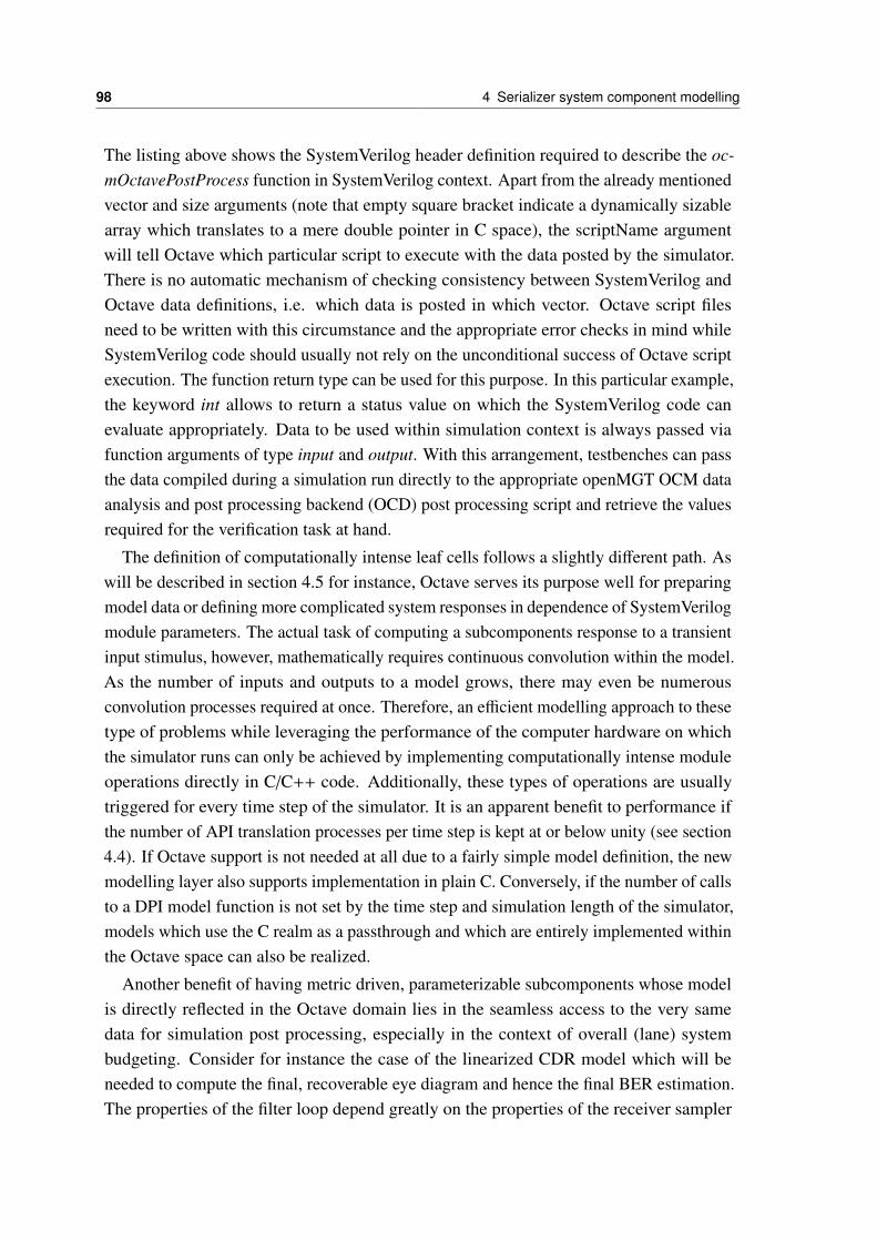
98 4 Serializer system component modelling
The listing above shows the SystemVerilog header definition required to describe the oc-mOctavePostProcess function in SystemVerilog context. Apart from the already mentionedvector and size arguments (note that empty square bracket indicate a dynamically sizablearray which translates to a mere double pointer in C space), the scriptName argumentwill tell Octave which particular script to execute with the data posted by the simulator.There is no automatic mechanism of checking consistency between SystemVerilog andOctave data definitions, i.e. which data is posted in which vector. Octave script filesneed to be written with this circumstance and the appropriate error checks in mind whileSystemVerilog code should usually not rely on the unconditional success of Octave scriptexecution. The function return type can be used for this purpose. In this particular example,the keyword int allows to return a status value on which the SystemVerilog code canevaluate appropriately. Data to be used within simulation context is always passed viafunction arguments of type input and output. With this arrangement, testbenches can passthe data compiled during a simulation run directly to the appropriate openMGT OCM dataanalysis and post processing backend (OCD) post processing script and retrieve the valuesrequired for the verification task at hand.
The definition of computationally intense leaf cells follows a slightly different path. Aswill be described in section 4.5 for instance, Octave serves its purpose well for preparingmodel data or defining more complicated system responses in dependence of SystemVerilogmodule parameters. The actual task of computing a subcomponents response to a transientinput stimulus, however, mathematically requires continuous convolution within the model.As the number of inputs and outputs to a model grows, there may even be numerousconvolution processes required at once. Therefore, an efficient modelling approach to thesetype of problems while leveraging the performance of the computer hardware on whichthe simulator runs can only be achieved by implementing computationally intense moduleoperations directly in C/C++ code. Additionally, these types of operations are usuallytriggered for every time step of the simulator. It is an apparent benefit to performance ifthe number of API translation processes per time step is kept at or below unity (see section4.4). If Octave support is not needed at all due to a fairly simple model definition, the newmodelling layer also supports implementation in plain C. Conversely, if the number of callsto a DPI model function is not set by the time step and simulation length of the simulator,models which use the C realm as a passthrough and which are entirely implemented withinthe Octave space can also be realized.
Another benefit of having metric driven, parameterizable subcomponents whose modelis directly reflected in the Octave domain lies in the seamless access to the very samedata for simulation post processing, especially in the context of overall (lane) systembudgeting. Consider for instance the case of the linearized CDR model which will beneeded to compute the final, recoverable eye diagram and hence the final BER estimation.The properties of the filter loop depend greatly on the properties of the receiver sampler

4.3 The openMGT C and Octave modelling extension (OCM) 99
(see section 5.3.6). While the transient simulation asserts correct functionality with respectto the signal flow of the design using sampler metrics as defined in the sampler leaf cellof the actual design, the very same parameters will be reflected in the numeric portion ofthe sampler model during post processing. This is a further example of how this particularapproach enforces consistency between the various simulation views of the sub- and overalldesign.
4.3.2 Self consistency of testbench and model
Stimulus Generation(Step)
Input and Output monitoringwith OCM routine
OCM Post ProcessingDeconvolution of output and input
compare equality
DUT - Amplifier (Model)
Z-Filter
Pole/ZeroInteger2BitVector BitVector2Real
Metrics as Parameters( ZeroN_lo ZeroN_hi )( PoleN_lo PoleN_hi )
compute expectedzeros/poles
constrain DUTmetrics via parameters
Frequency response fromimpulse response via FFT
Extract poles and zeros by numeric fit against prototype transfer function
Impulse response fromstep response via differentiation
Figure 4.4: Structure of the self consistent testbench and model development for amplifier transferfunction verification
As an example, an amplifier with adjustable zero and pole is modelled here. It is definedby two digital ports which translate the digital vector to real number variables whichin turn are input to a Z-filter module. The amplifier has a general section where inputcommon mode range and reference voltage range can be checked. The module receivesthe amplifier input data, converts it to single ended information and passes it on to theZ-Filter module. The required HDL code for the Z-Filter can readily be derived from thedirect type-II filter representation. Care must be taken not to propagate don’t-cares (x)into the IIR filter as this state will be irrecoverable. Therefore, as a reset and power down,resetting filter coefficients will reset the internal state. This of course is a very apparentdifference between the descriptions in the analog, time continuous and the real number

100 4 Serializer system component modelling
domain. Whereas in the first, the filter is stateless, the signal flow description of the secondmust necessarily be stateful.
The general testbench can send steps, pulses or PRBS streams into a DUT. Signalmonitors capture both in and output at simulator step time resolution. The signal monitorsuse DPI routines to transfer data to the Octave domain. Octave uses this data to derive thefrequency response from the step or pulse function (differentiation of the step response intime gives the according impulse response). The numeric backend then fits the transferfunction against equation 4.7 numerically. The resulting locations of poles and zeros mustmatch the model input parameters as given by model instantiation. Since the process ofcreating the model and probing its properties by testbench are vastly different and thenumeric domain of Octave is considered well checked with respect to implementationerrors, the testbench is implicitly assumed to extract the right metric while the model isshown to define the extracted metric in the proper manner. This also includes correctnessof the formulas derived for the generic three pole, two zero system of section 4.1 alongwith its SystemVerilog implementation. The result of the process can be seen in figure 4.5which shows an exemplary plot of a CTLE equalization stage.
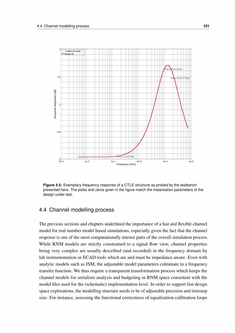
4.4 Channel modelling process 101
1e-3 1e-2 1e-1 1e+0 1e+1 1e+20
0.5
1
1.5
2
Frequency (GHz)
Res
pons
e M
agni
tude
(dB
)
Zero1: 0.133 GHz
Pole1: 9.224 GHz
Pole2: 16.477 GHz
Testbench dataModel fit
Figure 4.5: Exemplary frequency response of a CTLE structure as probed by the testbenchpresented here. The poles and zeros given in the figure match the instantiation parameters of thedesign under test.
4.4 Channel modelling process
The previous sections and chapters underlined the importance of a fast and flexible channelmodel for real number model based simulations, especially given the fact that the channelresponse is one of the most computationally intense parts of the overall simulation process.While RNM models are strictly constrained to a signal flow view, channel propertiesbeing very complex are usually described (and recorded) in the frequency domain bylab instrumentation or ECAD tools which are and must be impedance aware. Even withanalytic models such as JSM, the adjustable model parameters culminate in a frequencytransfer function. We thus require a transparent transformation process which keeps thechannel models for serializer analysis and budgeting in RNM space consistent with themodel files used for the (schematic) implementation level. In order to support fast designspace explorations, the modelling structure needs to be of adjustable precision and timestepsize. For instance, assessing the functional correctness of equalization calibration loops
102 4 Serializer system component modelling
with the two time constants of data rate and adaption loop which are spaced by a factor ofrouhgly a thousand may work with fairly coarse grained simulation resolution. The actualbudgeting procedure, however, will rely on much smaller timesteps to correctly estimatethe magnitude of residual inter symbol interference and the effects of equalization on theCDR sampling point. Finally, due to the strict separation of random and deterministiceffects in the openMGT framework, there will necessarily have to be numeric analysissteps in the OCM budgeting procedure (see section 5.3) which also need to have access tothe original channel frequency transfer function(s).
The openMGT OCM channel implementation attempts to solve these requirements inthe following way: The general idea is to mimic the channel as an FIR filter with its tapsgiven by the impulse response between two ports. This approach lends itself naturallyto the RNM modelling realm. It requires to prepare the data numerically given a setof general model parameters such as target precision or simulator time step. This onceobtained data is transferred to the C extension of the simulator where a custom convolutionimplementation then efficiently computes the channel responses for the input stimulusprovided by the SystemVerilog environment. These steps are outlined in the following ingreater detail and are also laid out graphically in figure 4.6.
Optimized C ConvolutionThreaded and SIMD extended
Data preparationConversion to Impulse Responseof proper resolution and precision
Stimulus Generation (Pulse)Input and Output monitoring
with OCM routine
OCM Post ProcessingFFT deconvolution of output and input
compare equality
DUT - Channel (Model)
SystemVerilogOCM Channel Module
frequency response andimpulse response
Model fileTouchstone (S-Param.)Impulse Response file
Octave definition, i.e. JSM
General model parametersPort InteractionsCoupling Mode
Impulse Rsp Precision
Model definition
frequency response andimpulse response
SystemVerilog Realm
OCM C RealmOCM Octave Realm
data syncport inputs
data syncport outputsParameters
OCM ChannelData Stash
Impulse Responseper port
Ports,Precision,Coupling mode
Figure 4.6: OCM channel modelling and testbench flow
4.4 Channel modelling process 103
4.4.1 OCM data preparation
The input data describing the channel can be of various origins which all must representa differentially coupled transmission line with its four ports. This sets the structuralrequirements to the schematic and SystemVerilog channel module/instance. The differentialports are combined by defining port 1 to be the positive node of the transmitter output, port3 to be the negative node of the transmitter output and ports 2 and 4 to be the positive andnegative input of the receiver respectively.
• The source can be a Touchstone file representing the single-ended S-Parameters ofthe four port. This is the most native model description as it is the direct counterpartto the schematic based, direct inclusion customly supported by ECAD tools.
• The origin of the data may also be an impulse response file (i.e. from a specification).It is assumed that this response was recorded with a differential channel. Bothtraces between port 1/2 and 3/4 will be assigned with the identical impulse response.Conceptually, this models two uncoupled traces of half the differential impedance.Since there are no EMI sources or aggressor nets in the RNM simulation (yet), thisabstraction step is considered to be permissible. Also, providing impulse responsefunctions is a more common thing among older, less demanding and slower serialstandards. Newer standards always define impedance masks in accordance to whichthe channel can be modelled with modern ECAD tools. They in turn then provideS-Parameter files as input to the procedure presented here.
• A third option is to describe the frequency transfer function with a numeric model.The Johnson Signal Model introduced in section 3.2 is an example of such a model. Itsfree model parameters can directly be specified within the SystemVerilog componentthereby ensuring consistency between transient simulation and subsequent numericalbudgeting.
Unless the impulse response is already given explicitly, it is numerically computedby Octave via an inverse Fourier transformation. Care must be taken with respect to thedefinition ranges of the input model data. The transfer functions which are usually givenfor the positive range of frequencies are first extended to negative frequencies. Since weassume the impulse response to be purely real, the real part of all frequency components issymmetrical about the y-axis, that is ReH(ω) = ReH(ω) and the imaginary part mustexhibit antisymmetry about the y-axis, that is ImH(ω) = −ImH(−ω). This effectivelydoubles the transformation window and perturbations due to the limited window size ofthe discrete transformation process are reduced. The resolution and length of the resultingimpulse response will of course depend on the highest frequency content of the transferfunction and on its resolution (refer to equations 2.2 and 2.3 in section 2.1 ).

104 4 Serializer system component modelling
Usually, start frequency fs and resolution fr of ECAD or lab instrument provided datais the same and sets the length of the computed impulse response. Since we are mostinterested in the high frequency properties of the transmission channels, the constraints onfs itself are fairly moderate as long as the propagation delay of the channel and thereforethe round trip time for resonance induced ISI is not too large. A range between 5−50 MHzis usually sufficient. As far as fr is concerned, however, a low value around 5 − 10 MHz ispreferable in order to capture the various potential resonances in the frequency transferfunction. The stop frequency fe on the other hand needs to be chosen such that fe is wellbeyond the Nyquist frequency fNy =
12T of interest. This allows a good impulse response
resolution to capture the various discontinuities in the channel for a correct prediction ofISI.
In order to find a reasonable constraint for fe, section 3.4 about the PSD of NRZ testpatterns provides valuable insight. It can be seen that the main lobe of power in the signaldrops to zero at ω = 2 fNy. There is a second lope starting at this point and reaching toω = 4 fNy. However, its power is just a fraction compared to the main lobe (five versusninety percent, which can also be seen from figure 3.23 in section 3.4). Furthermore,channels with strong attenuation already at the Nyquist frequency will diminish thisfraction of spectral power content even further. The highest frequency content in the dataprovided to the OCM framework may therefore be limited to twice the Nyquist frequencyof the highest data rate to be supported by the serializer system.
The channels impulse response taken directly from the inverse Fourier transformationmight be a very long vector. In order to comply with the simulator time steps which can betuned to trade off precision for performance, the numeric backend may additionally haveto resample and truncate the impulse response. The resampling process needs to assurethat the power integral of the impulse response
P(x) =N−1∑n=0
‖x[n]‖ · ∆t
stays constant. Naturally, the contribution per tap will therefore scale down with thenumber of taps per unit time. If the simulator time steps are small compared to theresponse duration the resulting vector of double precision values will be very long. From aconvolution standpoint, however, the important section even of a very dispersive channel isfairly short. In order to decrease the vector dot product operations (to which the convolutionessentially boils down to) the FIR tap vector should be as small as possible. This is what ismeant by impulse response precision: the general model parameter describes how largethe magnitude of the impulse response at a certain sampling point (tap location) must berelative to its maximum so that it is considered relevant. Defining the parameter of impulseresponse precision relative to the response maximum allows to support different simulator
4.4 Channel modelling process 105
time steps without changing model parameters.The truncation procedure clips the impulse response from start and end towards the
pulse and stops once it encounters a relevant tap. For long channels with strong reflections,this procedure may still lead to fairly long responses from pulse peak to end. On theother hand, the large propagation delay of long channels will mirror in a long sequenceof quiesce leading up to the impulse peak. In contrast to the tailing sequence, the lead insequence can, however, not simply be truncated since these taps reflect the propagationdelay of the physical channel.
On high performance computer hardware, the transformation and resampling processesdo not take up much time. Octave uses advanced open source libraries to implement theseprocedures in a very efficient way. Nevertheless, during development of system componentswhich rely on a channel model to be tested with, regenerating the model data on everysimulation run would proof tedious after a while. Therefore, if the general parameters of achannel with a given Touchstone file are not changed in the SystemVerilog code (which isthe location they are defined at, see below), the required impulse responses are drawn froma disk storage area called the OCM stash to avoid unnecessary recomputation.
4.4.2 Optimized C convolution routine
The C channel convolution routine receives its parameters from both the SystemVerilog andthe Octave OCM domain. While SystemVerilog derlivers all general and model parametersfor the channel instance, the C routine passes all parameters required for impulse responsegeneration on to the OCM domain. In turn, it receives the truncated impulse response.The noncontributing delay taps of the channel propagation delay are truncated from themain impulse response, too, but are also reported to the C routine. It will allocate acorresponding amount of memory for buffering up and delaying the stream of real numbervalues incident on the SystemVerilog components ports. With a sequence of further generalmodel parameters, the C convolution code and the data preparation of the numeric backendallow the explicit definition of which port interactions described by the model file willactually be considered for simulation. A real number simulation with a long, dispersivechannel with weak coupling between the traces may for instance be plainly modelled byits forward S-Parameters S 21 and S 43. If coupling in forward direction (from TX to RX)between the traces is to be considered, S 41 and S 32 may for instance also be of interest.The general parameter named coupling mode on the other hand allows to numericallycompute the mixed-mode S-Parameters of the coupled structure which could then again beused to reduce the number of port interactions to merely two again (S dd21 twice for bothtraces of the differential pair channel model).
In order to speed up the convolution procedure, three distinct optimization conceptshave been implemented in the custom C code:
106 4 Serializer system component modelling
• A ring buffer per port interaction to model initial channel delay and avoid memorycopies. Apart from being far more efficient than a SystemVerilog real value delaychain, it also allows to accept a flexible number of data samples per API call (see thesubsection below).
• The vector dot product operation for convolution is implemented using specificSIMD instructions.1 It is also implemented in a general way with floating pointvalues of double precision to support all CPU types. The degree of architectureindependent GNU C Compiler optimization flags has been tuned and analyzed forbest performance.
• There is one POSIX thread spawned per requested port interaction. This essentiallyparallelizes an otherwise single threaded SystemVerilog simulator and therefore usesthe performance potential of modern hyperthreaded or multicore machines to a muchbetter extent.
The role of the OCM C code is actually twofold. During initialization it accepts datafrom the SystemVerilog domain and triggers the Octave backend data preparation processfrom which it in turn reads back the impulse responses and the number of delay taps.During simulation, it then distributes the incoming stream of data to the appropriatethreads, gathers their results and hands the data back accordingly.
4.4.3 SystemVerilog considerations
Conceptually, the SystemVerilog channel module ports are input and output at the sametime. The port interaction definitions which are a part of the general model parameterscontained in the SystemVeriog code, permit to define a port as both source or destinationand even both at the same time. This is also necessary because of the S-Parameter returnlosses S NN which can then be included in the modelling process as well if need be. During asimulator time step, the current voltage levels, represented by a real number on the modulesfour inputs, are saved by the module into a common array of four real items. The modulethen executes the optimized OCM channel convolution function with a SystemVerilog DPIcall thereby passing over control to the custom C code extension. The new data items arepassed by using the common real array as the functions first argument. In the C domain, itcan be accessed by a simple double pointer and can thus be written into the respective ringbuffers as described above. The collected results from the various threads are combinedfor each destination port and written back to the SystemVerilog simulator. This is done byspecifying a second real array common to all ports and passing it as the second argumentof the convolution function call. Once the DPI function call returns, the values in the
1 On the Intel machines used in this thesis, these are AVX or SSE instructions

4.4 Channel modelling process 107
second array can be passed on to the respective module ports by continuous assignment.The following code listings show the SystemVerilog definition of the channel convolutionfunction as well as a fraction of the SystemVerilog model code to more accurately conveythe whole picture.
The SystemVerilog DPI call is defined in the following way.
import "DPI-C" function void ocmChannelConvolutionStep (
input real portsIn[`OMGT_OCM_SYNC_WORDS*4-1:0],
inout real portsOut[`OMGT_OCM_SYNC_WORDS*4-1:0]
);
The SystemVerilog module parameters and real input arrays allow direct manipulationof the specific model to be used, its options (such as source file), further arguments to anumeric model (such as those required by the Johnson signal model) and of course thegeneral parameters of the modelling process which define model accuracy and the requiredport interactions (for an explanation of the sync word mechanism, see below).
module MGT_MODEL_CHANNEL #(
parameter string MODEL_TYPE = "", // SXP or JSM
parameter string MODEL_DESC = "",
parameter int NUM_MODEL_ARGS = 16, // number channel model arguments
parameter int NUM_PARAMS = 16 // number of general model params
)
(
input wrealsum IN_N, // aka. port 3
input wrealsum IN_P, // aka. port 1
output wrealsum OUT_N, // aka. port 4
output wrealsum OUT_P, // aka. port 2
inout wreal REF,
input real params[NUM_PARAMS -1:0],
input real mdlArgs[NUM_MODEL_ARGS -1:0]
);
...
initial begin
cid = ocmCreateChannel(MODEL_TYPE , MODEL_DESC , params, NUM_PARAMS , mdlArgs, NUM_MODEL_ARGS);
...
forever begin
...
if(i == `OCM_SYNC_WORDS ) begin
...
ocmChannelConvolutionStep(port_hist_in , port_hist_out);
...
end
...
end
...
endmodule
This arrangement evidently creates a situation in which it is very likely to have at leasttwo drivers on a single wire. The first may for instance be the driver modelling transmitteroutput voltage contribution, the second would be the reflected voltage of the channel port.Therefore, the module ports are defined as being of type wrealsum. Wrealsum is a builtinSystemVerilog wire type whose resolution function simply adds the contributions of alldrivers attached to a net which matches very nicely with the principle of superposition ofelectromagnetic waves.
At this point, one might question the sensibility of this approach by arguing that decentring buffer and filter structures can of course be implemented by Verilog and thus Sys-
108 4 Serializer system component modelling
temVerilog as well. Also, as explained in section 4.1 it is of course possible to create FIRstructures entirely in System Verilog alone. However, for long, dispersive channels withstrong reflections, the impulse responses tend to become fairly long. Additionally, the FIRtap weights would need to be initialized in accordance with the calculated impulse response- a step which would necessitate the extension of the resulting model with some sort of DPIcall back as well. Furthermore, a flexible number of port interactions would need to berealized by cumbersome generate blocks or precompiler flags. The only potential way tocircumvent these pitfalls would be to use a scripting language which generates specificSystemVerilog modules with hardcoded FIR tap weights from a given model file and underconsideration of general model parameters defined in an additional file. Also, the resultingmodule would solely be restricted to the specific simulator time step resolution at handand would require regeneration whenever the resolution was changed. Last but not least,there is no real number vector multiplication support in SystemVerilog2012 whatsoever.The FIR structure would need to be written down (or generated) explicitly. Depending onthe number of required port interactions, there would be a considerable amount of realregisters, adders and multipliers involved to mimic the process of convolution. Given thatcurrent SystemVerilog simulators are still single threaded programs, parallelization or anymachine dependent optimization would of course not be possible at all.
Therefore using the DPI extension with its vector access functions results in the fastestand most flexible method of modelling transmission channels in a signal flow based viewfor RNM simulations. There is, however, a slight drawback to this solution if implementedexactly the way described above:
Every DPI call triggers a sequence of simulator intrinsic mechanisms which take careof translation processes and data consistency checks. If the C code executes very fastcompared to the DPI call itself, this produces an intolerable amount of overhead. Especiallyif optimization schemes such as SIMD instructions or threaded execution are to be of anybenefit, the translation process between SystemVerilog and C domain must be diminishedin its temporal extent compared to the convolution computation time. This can actually beachieved by data aggregation. Instead of calling the convolution function on every timestep, data is collected for a parameterizable amount of time and transferred to the C domainat once. The same function call also returns the computed values - the synchronizationwords - for the future time steps.
For port interactions whose impulse response displays a considerable amount of delay(that is, a sequence of taps below the significance threshold), the amount of synchronizationwords can simply be deducted from the required amount of delay taps and the synchro-nization mechanism will have no apparent effect on the correctness of the channel portinteraction. For return losses S NN however, this procedure is of course not accurate sinceinput stimulus and resulting reflection are physically immediate. In the context of serializer
4.4 Channel modelling process 109
design space exploration, however, we are mostly interested in the transfer properties ofthe channel. Real number models do not capture the notion of impedance and it wouldcertainly be a challenging task to model the multiple reflections occuring at a severelymismatched port with strong return loss within RNM context. For final performanceevaluation of a system implementation, one may also revert back to true S-Parameter basedsimulation in order to capture these impedance related effects. As far as the analysis andverification targets of real number modelling are concerned, however, the ansatz presentedhere provides enough accuracy and captures the most dominant effects.
As can also be seen from the module code listing above, the channel initialization mustalso be initiated by the specific channel instance. The module parameters, both modelspecific and general, are passed to the numeric backend which computes the requiredimpulse responses accordingly and triggers the memory allocation processes in the Cdomain. This mechanism allows to realize all required flexibility in the numeric backendincluding adjustable simulator time steps and therefore accuracy. It also ensures that thechannel model used for post simulation budgeting will work with the same model data asits preceding transient simulation (see section 5.3).
4.4.4 Testbench and performance comparison
Following the general design idea of the openMGT framework, the channel testbenchneeds to assert correctness of the channel model presented here. It also needs to proofreasonable equivalence of the real number model signal flow view and the schematic repre-sentation, that is, the vendor implementation of S-Parameter integration in analog transientsimulations. The arguably complex modelling scheme may lead to implementation errorsat various different levels. Surely, the numeric backend data preparation is based on maturecode as Octave itself is based on well-established open source libraries (i.e. the openBLASlibrary for linear algebra or the fftw library for Fourier transformation). Nevertheless,correct data preparation such as resampling are prone to result in scaling error if handledincorrectly. More importantly, it is the custom C convolution routine based on SIMDinstructions which needs to be tested thoroughly.
To this end, a pulse response testbench is used. The stimulus generator is written inSystemVerilog. It directly stimulates the transmission ports 1 and 3 of the test channelin the real number model case. For schematic based simulations, a connect module isresponsible for correct conversion to behave like a voltage mode driver of well-definedoutput impedance. The termination of the output ports 2 and 4 simply mimics the DC volt-age division in the RNM case whereas in the schematic based simulation, the terminationmodule is swapped for a schematic based implementation. Both input and output of thechannel module are recorded over time by SystemVerilog modules called monitors. They,too, use an OCM routine to transfer the recorded data to the numeric backend once the

110 4 Serializer system component modelling
simulation finishes. In the numeric backend, the post processing routine is triggered whichuses Fourier transformation based deconvolution to numerically reconstruct the impulseresponse of the DUT. The recovered and original model impulse responses can then becompared for equality. For improved visual comparability here, the impulse responsesare again Fourier transformed to present a more intuitive picture of the frequency transferfunctions magnitude plot.
This closes the circle of model and testbench development. Exemplary results for thisprocedure are given in figures 4.7 and 4.8 for the analog schematic based and real numbermodel based representation of a CEI28-MR channel respectively.
0 50 100 150 200 250-0.002
0
0.002
0.004
0.006
0.008
0.01
0.012
Time (ns)
Res
pons
e M
agni
tude
(V
/V)
From deconvolutionOriginal model data
0 5e+09 1e+10 1.5e+10 2e+10 2.5e+10 3e+10-40
-30
-20
-10
0
Frequency (GHz)
Res
pons
e M
agni
tude
(dB
)
From deconvolutionOriginal model data
Channel impulse response
Channel frequency response
Figure 4.7: Impulse response and frequency transfer function of the deconvoluted full analogsimulation together with the original S-Parameter data
From figure 4.8 it can be seen that the RNM modelling and simulation process producesa good agreement (apart from a mild, pessimistic DC offset) with original model datawhen a simulator time step and therefore FIR step resolution of 1 ps is chosen. The vendorsupplied analog convolution process on the other hand indicates an optimistic DC offset
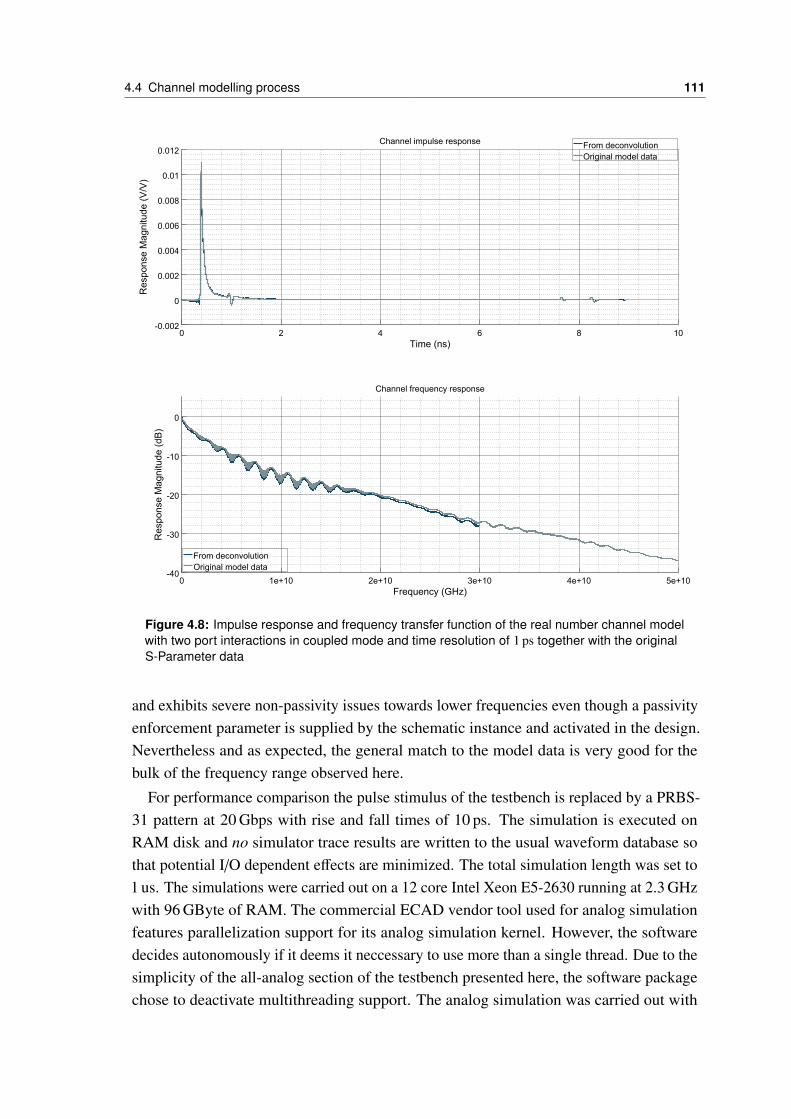
4.4 Channel modelling process 111
0 2 4 6 8 10-0.002
0
0.002
0.004
0.006
0.008
0.01
0.012
Time (ns)
Res
pons
e M
agni
tude
(V
/V)
From deconvolutionOriginal model data
0 1e+10 2e+10 3e+10 4e+10 5e+10-40
-30
-20
-10
0
Frequency (GHz)
Res
pons
e M
agni
tude
(dB
)
From deconvolutionOriginal model data
Channel impulse response
Channel frequency response
Figure 4.8: Impulse response and frequency transfer function of the real number channel modelwith two port interactions in coupled mode and time resolution of 1 ps together with the originalS-Parameter data
and exhibits severe non-passivity issues towards lower frequencies even though a passivityenforcement parameter is supplied by the schematic instance and activated in the design.Nevertheless and as expected, the general match to the model data is very good for thebulk of the frequency range observed here.
For performance comparison the pulse stimulus of the testbench is replaced by a PRBS-31 pattern at 20 Gbps with rise and fall times of 10 ps. The simulation is executed onRAM disk and no simulator trace results are written to the usual waveform database sothat potential I/O dependent effects are minimized. The total simulation length was set to1 us. The simulations were carried out on a 12 core Intel Xeon E5-2630 running at 2.3 GHzwith 96 GByte of RAM. The commercial ECAD vendor tool used for analog simulationfeatures parallelization support for its analog simulation kernel. However, the softwaredecides autonomously if it deems it neccessary to use more than a single thread. Due to thesimplicity of the all-analog section of the testbench presented here, the software packagechose to deactivate multithreading support. The analog simulation was carried out with
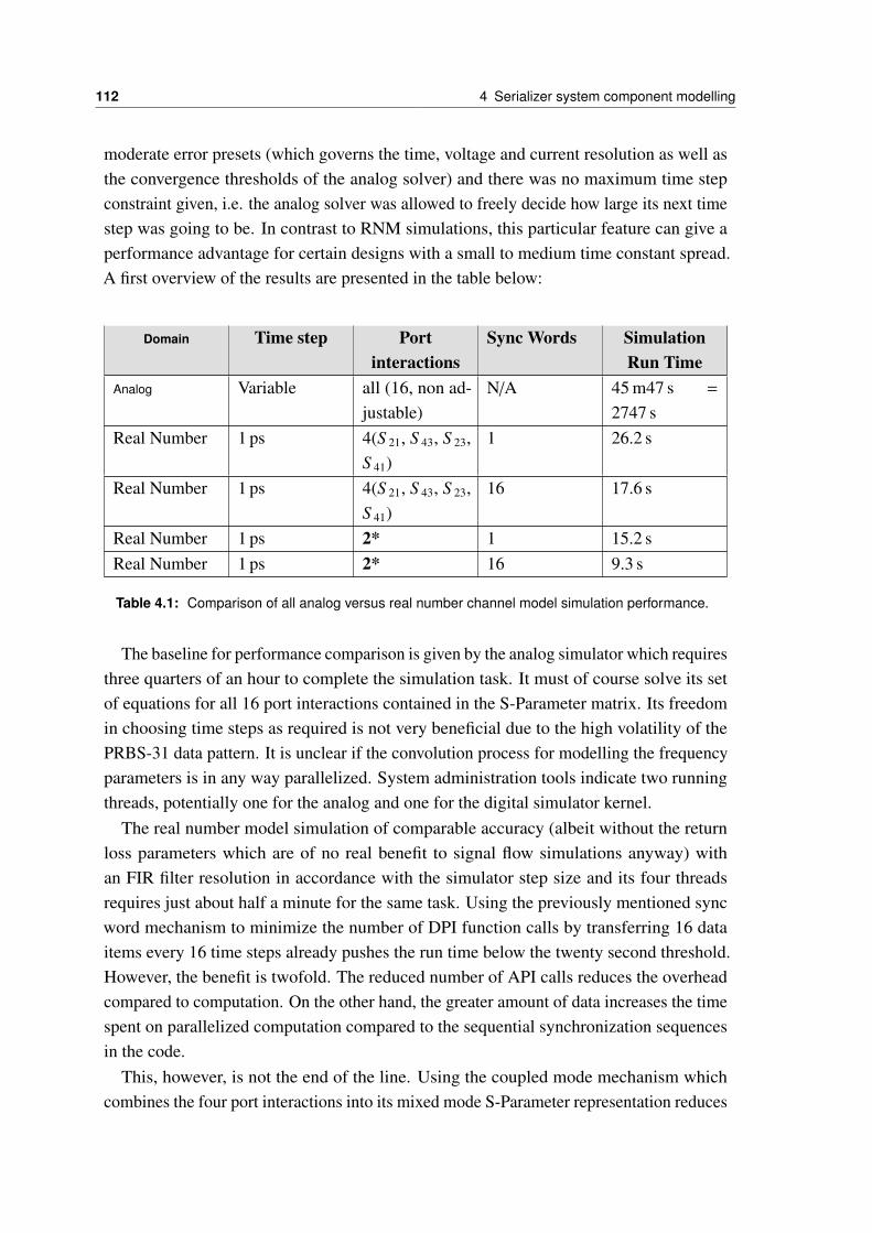
112 4 Serializer system component modelling
moderate error presets (which governs the time, voltage and current resolution as well asthe convergence thresholds of the analog solver) and there was no maximum time stepconstraint given, i.e. the analog solver was allowed to freely decide how large its next timestep was going to be. In contrast to RNM simulations, this particular feature can give aperformance advantage for certain designs with a small to medium time constant spread.A first overview of the results are presented in the table below:
Domain Time step Portinteractions
Sync Words SimulationRun Time
Analog Variable all (16, non ad-justable)
N/A 45 m47 s =
2747 sReal Number 1 ps 4(S 21, S 43, S 23,
S 41)1 26.2 s
Real Number 1 ps 4(S 21, S 43, S 23,S 41)
16 17.6 s
Real Number 1 ps 2* 1 15.2 sReal Number 1 ps 2* 16 9.3 s
Table 4.1: Comparison of all analog versus real number channel model simulation performance.
The baseline for performance comparison is given by the analog simulator which requiresthree quarters of an hour to complete the simulation task. It must of course solve its setof equations for all 16 port interactions contained in the S-Parameter matrix. Its freedomin choosing time steps as required is not very beneficial due to the high volatility of thePRBS-31 data pattern. It is unclear if the convolution process for modelling the frequencyparameters is in any way parallelized. System administration tools indicate two runningthreads, potentially one for the analog and one for the digital simulator kernel.
The real number model simulation of comparable accuracy (albeit without the returnloss parameters which are of no real benefit to signal flow simulations anyway) withan FIR filter resolution in accordance with the simulator step size and its four threadsrequires just about half a minute for the same task. Using the previously mentioned syncword mechanism to minimize the number of DPI function calls by transferring 16 dataitems every 16 time steps already pushes the run time below the twenty second threshold.However, the benefit is twofold. The reduced number of API calls reduces the overheadcompared to computation. On the other hand, the greater amount of data increases the timespent on parallelized computation compared to the sequential synchronization sequencesin the code.
This, however, is not the end of the line. Using the coupled mode mechanism whichcombines the four port interactions into its mixed mode S-Parameter representation reduces
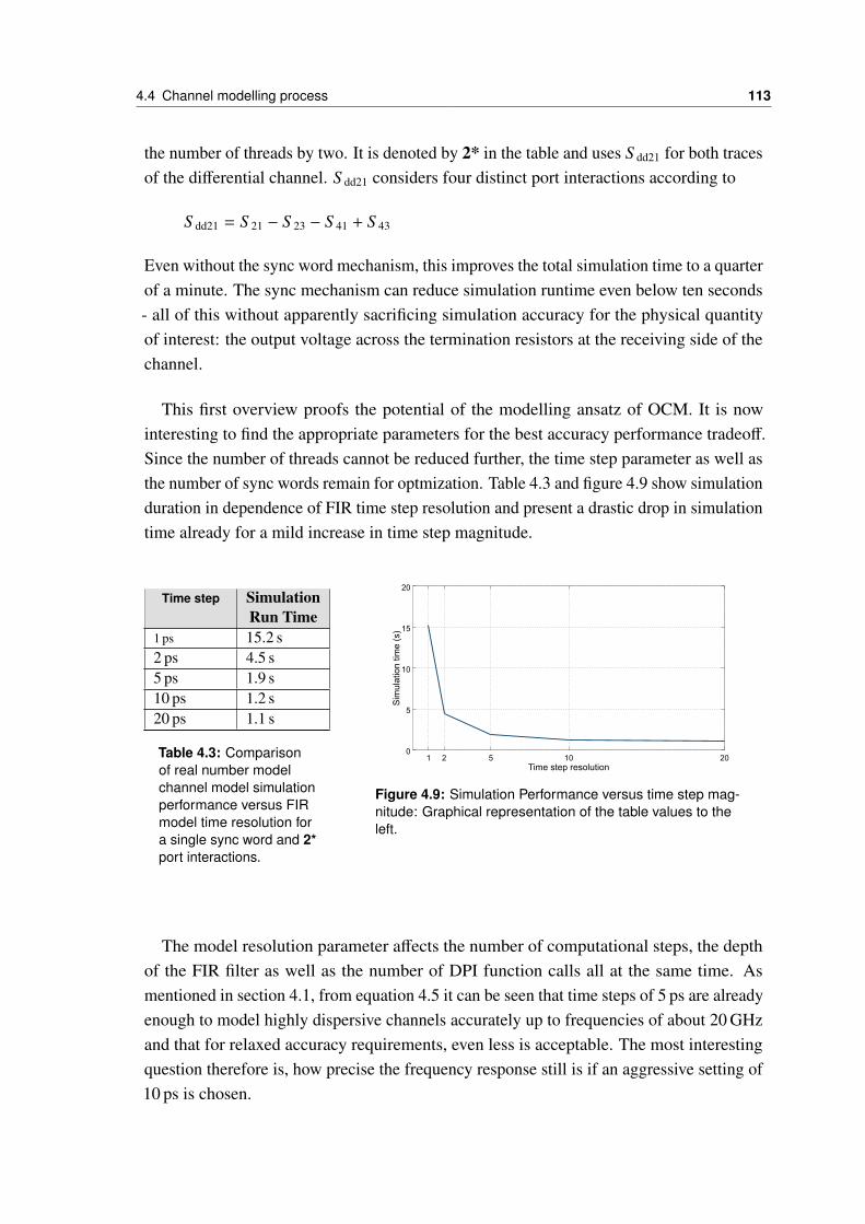
4.4 Channel modelling process 113
the number of threads by two. It is denoted by 2* in the table and uses S dd21 for both tracesof the differential channel. S dd21 considers four distinct port interactions according to
S dd21 = S 21 − S 23 − S 41 + S 43
Even without the sync word mechanism, this improves the total simulation time to a quarterof a minute. The sync mechanism can reduce simulation runtime even below ten seconds- all of this without apparently sacrificing simulation accuracy for the physical quantityof interest: the output voltage across the termination resistors at the receiving side of thechannel.
This first overview proofs the potential of the modelling ansatz of OCM. It is nowinteresting to find the appropriate parameters for the best accuracy performance tradeoff.Since the number of threads cannot be reduced further, the time step parameter as well asthe number of sync words remain for optmization. Table 4.3 and figure 4.9 show simulationduration in dependence of FIR time step resolution and present a drastic drop in simulationtime already for a mild increase in time step magnitude.
Time step SimulationRun Time
1 ps 15.2 s2 ps 4.5 s5 ps 1.9 s10 ps 1.2 s20 ps 1.1 s
Table 4.3: Comparisonof real number modelchannel model simulationperformance versus FIRmodel time resolution fora single sync word and 2*port interactions.
100
5
10
15
20
Time step resolution
Sim
ulat
ion
tim
e (
s)
521 20
Figure 4.9: Simulation Performance versus time step mag-nitude: Graphical representation of the table values to theleft.
The model resolution parameter affects the number of computational steps, the depthof the FIR filter as well as the number of DPI function calls all at the same time. Asmentioned in section 4.1, from equation 4.5 it can be seen that time steps of 5 ps are alreadyenough to model highly dispersive channels accurately up to frequencies of about 20 GHzand that for relaxed accuracy requirements, even less is acceptable. The most interestingquestion therefore is, how precise the frequency response still is if an aggressive setting of10 ps is chosen.
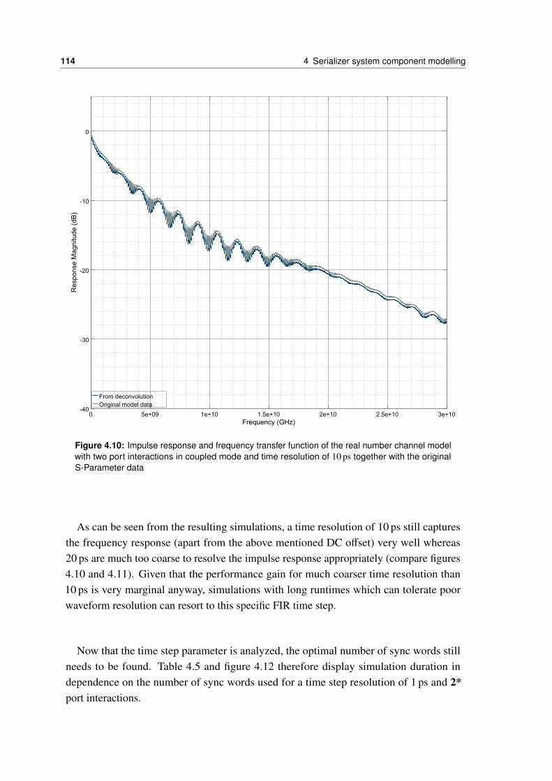
114 4 Serializer system component modelling
0 5e+09 1e+10 1.5e+10 2e+10 2.5e+10 3e+10-40
-30
-20
-10
0
Frequency (GHz)
Res
pons
e M
agni
tude
(dB
)
From deconvolutionOriginal model data
Figure 4.10: Impulse response and frequency transfer function of the real number channel modelwith two port interactions in coupled mode and time resolution of 10 ps together with the originalS-Parameter data
As can be seen from the resulting simulations, a time resolution of 10 ps still capturesthe frequency response (apart from the above mentioned DC offset) very well whereas20 ps are much too coarse to resolve the impulse response appropriately (compare figures4.10 and 4.11). Given that the performance gain for much coarser time resolution than10 ps is very marginal anyway, simulations with long runtimes which can tolerate poorwaveform resolution can resort to this specific FIR time step.
Now that the time step parameter is analyzed, the optimal number of sync words stillneeds to be found. Table 4.5 and figure 4.12 therefore display simulation duration independence on the number of sync words used for a time step resolution of 1 ps and 2*port interactions.
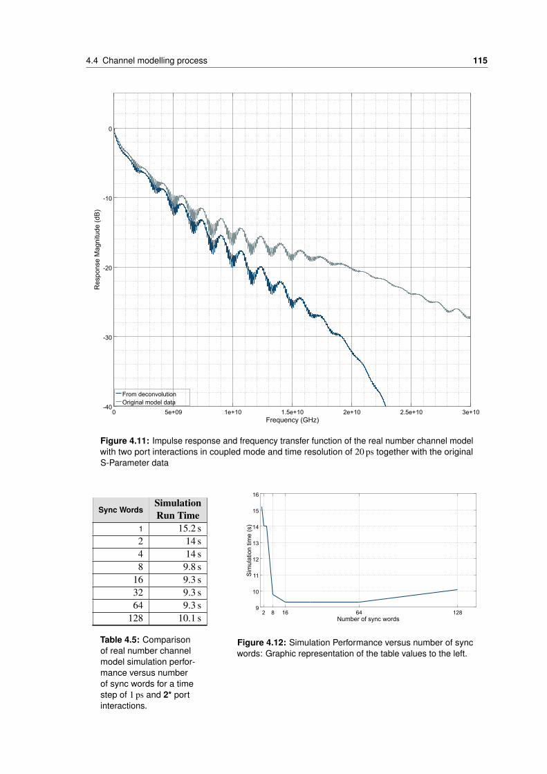
4.4 Channel modelling process 115
0 5e+09 1e+10 1.5e+10 2e+10 2.5e+10 3e+10-40
-30
-20
-10
0
Frequency (GHz)
Res
pons
e M
agni
tude
(dB
)
From deconvolutionOriginal model data
Figure 4.11: Impulse response and frequency transfer function of the real number channel modelwith two port interactions in coupled mode and time resolution of 20 ps together with the originalS-Parameter data
Sync WordsSimulationRun Time
1 15.2 s2 14 s4 14 s8 9.8 s
16 9.3 s32 9.3 s64 9.3 s
128 10.1 s
Table 4.5: Comparisonof real number channelmodel simulation perfor-mance versus numberof sync words for a timestep of 1 ps and 2* portinteractions.
11
12
13
14
15
16
Number of sync words
Sim
ulat
ion
tim
e (
s)
9128641682
10
Figure 4.12: Simulation Performance versus number of syncwords: Graphic representation of the table values to the left.

116 4 Serializer system component modelling
For the number of synchronization words between C and SystemVerilog domain, thereseems to be a sweet spot for word counts between 16 and 64. Since there are four ports,the number of transmitted real values is actually between 64 and 256 per direction. Sincethe SystemVerilog real values find their C counterpart in floating point values of doubleprecision which are represented by eight bytes on the x86 64-bit architecture, the numberof accessed bytes in either direction are between 1 to 4 kByte. The latter is the page sizeof the Linux operating system which could be one reason why performance starts to dropagain with an increase in sync words. It could, however also be simply related to the wayin which simulator internal data structures are defined.
The best overall choices considering both optimization processes are thus given in table4.6 and will be used for the equalization and calibration procedures within the openMGTdesign and budgeting framework. A resolution of 1 ps is used whenever budgeting effortsplay an important role within the simulation context and slower simulation speed isaccepted in favor of a better signal transition resolution. A resolution of 5 ps with 16 syncwords will be used for simulations with large time constant spread such as equalizationtraining loop analysis. For these simulations, the presented modelling procedure offers aperformance factor of 1830 compared to traditional all analog simulation with moderateaccuracy presets.
Time step Port in-teractions
SyncWords
Simula-tion Run
Time1 ps 2* 16 9.3 s2 ps 2* 16 3.7 s5 ps 2* 16 1.5 s10 ps 2* 1 1.4 s
Table 4.6: Optimized real number channel model simulation performance
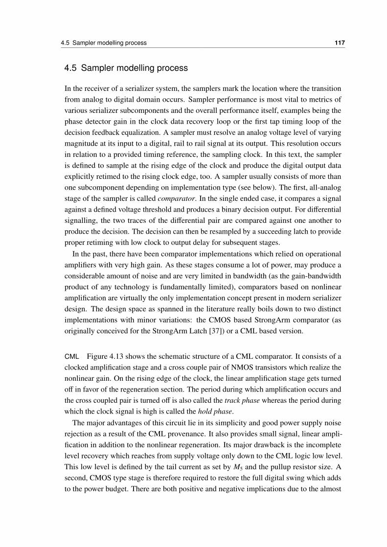
4.5 Sampler modelling process 117
4.5 Sampler modelling process
In the receiver of a serializer system, the samplers mark the location where the transitionfrom analog to digital domain occurs. Sampler performance is most vital to metrics ofvarious serializer subcomponents and the overall performance itself, examples being thephase detector gain in the clock data recovery loop or the first tap timing loop of thedecision feedback equalization. A sampler must resolve an analog voltage level of varyingmagnitude at its input to a digital, rail to rail signal at its output. This resolution occursin relation to a provided timing reference, the sampling clock. In this text, the sampleris defined to sample at the rising edge of the clock and produce the digital output dataexplicitly retimed to the rising clock edge, too. A sampler usually consists of more thanone subcomponent depending on implementation type (see below). The first, all-analogstage of the sampler is called comparator. In the single ended case, it compares a signalagainst a defined voltage threshold and produces a binary decision output. For differentialsignalling, the two traces of the differential pair are compared against one another toproduce the decision. The decision can then be resampled by a succeeding latch to provideproper retiming with low clock to output delay for subsequent stages.
In the past, there have been comparator implementations which relied on operationalamplifiers with very high gain. As these stages consume a lot of power, may produce aconsiderable amount of noise and are very limited in bandwidth (as the gain-bandwidthproduct of any technology is fundamentally limited), comparators based on nonlinearamplification are virtually the only implementation concept present in modern serializerdesign. The design space as spanned in the literature really boils down to two distinctimplementations with minor variations: the CMOS based StrongArm comparator (asoriginally conceived for the StrongArm Latch [37]) or a CML based version.
CML Figure 4.13 shows the schematic structure of a CML comparator. It consists of aclocked amplification stage and a cross couple pair of NMOS transistors which realize thenonlinear gain. On the rising edge of the clock, the linear amplification stage gets turnedoff in favor of the regeneration section. The period during which amplification occurs andthe cross coupled pair is turned off is also called the track phase whereas the period duringwhich the clock signal is high is called the hold phase.
The major advantages of this circuit lie in its simplicity and good power supply noiserejection as a result of the CML provenance. It also provides small signal, linear ampli-fication in addition to the nonlinear regeneration. Its major drawback is the incompletelevel recovery which reaches from supply voltage only down to the CML logic low level.This low level is defined by the tail current as set by M5 and the pullup resistor size. Asecond, CMOS type stage is therefore required to restore the full digital swing which addsto the power budget. There are both positive and negative implications due to the almost
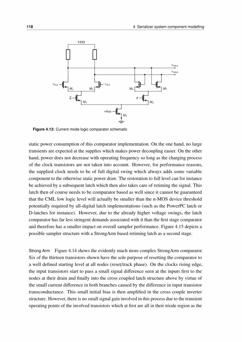
118 4 Serializer system component modelling
VDD
M1
vin,p
M2
vin,n
vout,n
vout,p
M6 M7
M4
φ
M3
φ
M5
vbias
Figure 4.13: Current mode logic comparator schematic
static power consumption of this comparator implementation. On the one hand, no largetransients are expected at the supplies which makes power decoupling easier. On the otherhand, power does not decrease with operating frequency so long as the charging processof the clock transistors are not taken into account. However, for performance reasons,the supplied clock needs to be of full digital swing which always adds some variablecomponent to the otherwise static power draw. The restoration to full level can for instancebe achieved by a subsequent latch which then also takes care of retiming the signal. Thislatch then of course needs to be comparator based as well since it cannot be guaranteedthat the CML low logic level will actually be smaller than the n-MOS device thresholdpotentially required by all-digital latch implementations (such as the PowerPC latch orD-latches for instance). However, due to the already higher voltage swings, the latchcomparator has far less stringent demands associated with it than the first stage comparatorand therefore has a smaller impact on overall sampler performance. Figure 4.15 depicts apossible sampler structure with a StrongArm based retiming latch as a second stage.
Strong Arm Figure 4.14 shows the evidently much more complex StrongArm comparator.Six of the thirteen transistors shown have the sole purpose of resetting the comparator toa well defined starting level at all nodes (reset/track phase). On the clocks rising edge,the input transistors start to pass a small signal difference seen at the inputs first to thenodes at their drain and finally into the cross coupled latch structure above by virtue ofthe small current difference in both branches caused by the difference in input transistortransconductance. This small initial bias is then amplified in the cross couple inverterstructure. However, there is no small signal gain involved in this process due to the transientoperating points of the involved transistors which at first are all in their triode region as the
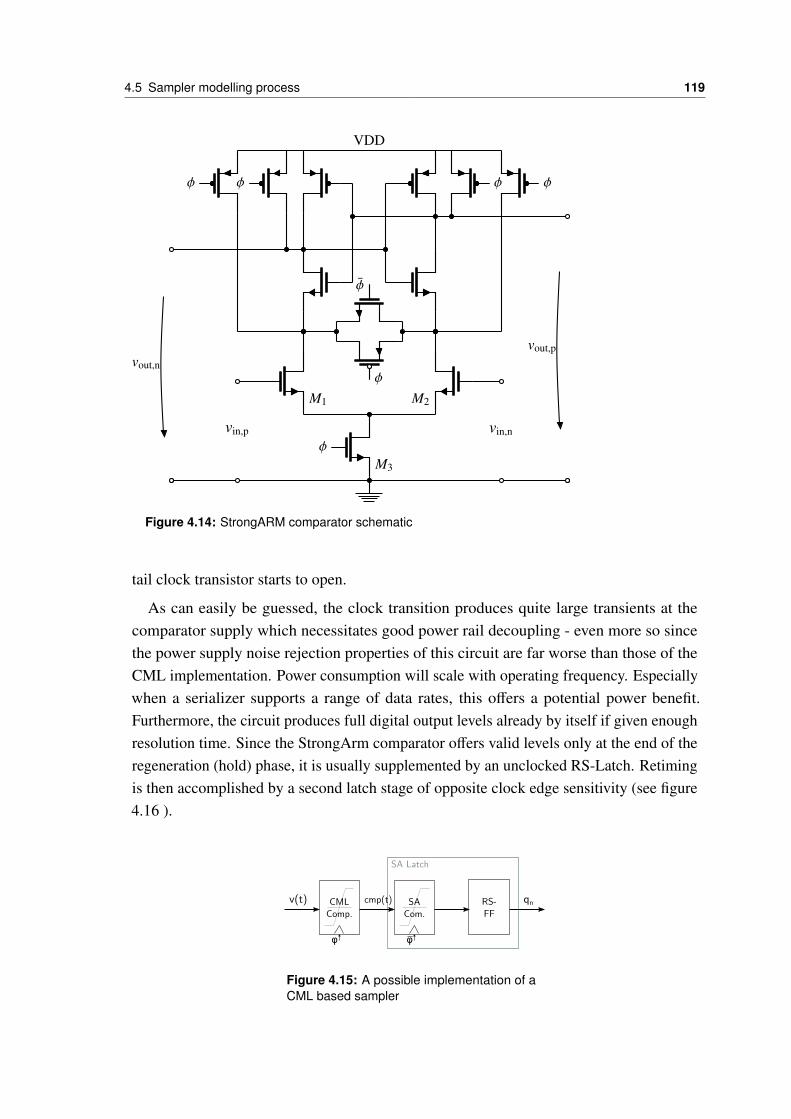
4.5 Sampler modelling process 119
VDD
φφ φ φ
vout,pvout,n
φ
φ
M1 M2
vin,p vin,n
M3
φ
Figure 4.14: StrongARM comparator schematic
tail clock transistor starts to open.
As can easily be guessed, the clock transition produces quite large transients at thecomparator supply which necessitates good power rail decoupling - even more so sincethe power supply noise rejection properties of this circuit are far worse than those of theCML implementation. Power consumption will scale with operating frequency. Especiallywhen a serializer supports a range of data rates, this offers a potential power benefit.Furthermore, the circuit produces full digital output levels already by itself if given enoughresolution time. Since the StrongArm comparator offers valid levels only at the end of theregeneration (hold) phase, it is usually supplemented by an unclocked RS-Latch. Retimingis then accomplished by a second latch stage of opposite clock edge sensitivity (see figure4.16 ).
CMLComp.
SACom.
φφ
RS-FF
v(t) cmp(t) qn
SA Latch
Figure 4.15: A possible implementation of aCML based sampler
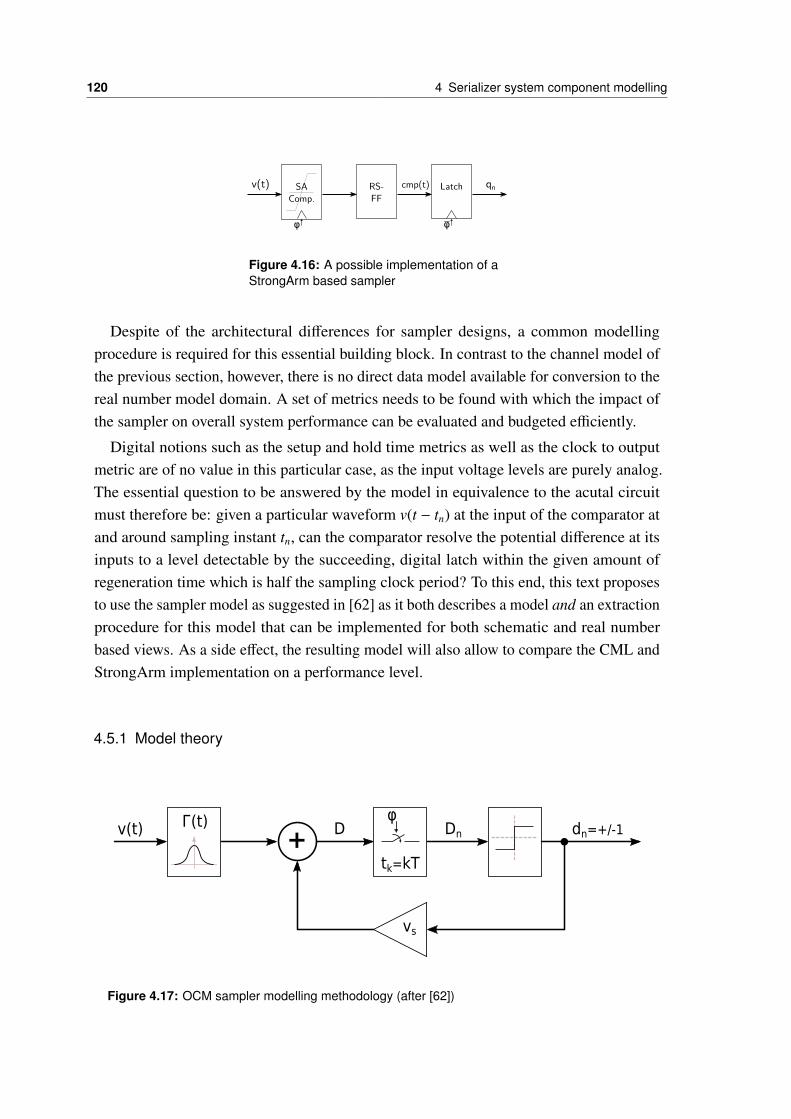
120 4 Serializer system component modelling
SAComp.
Latch
φφ
RS-FF
v(t) cmp(t) qn
Figure 4.16: A possible implementation of aStrongArm based sampler
Despite of the architectural differences for sampler designs, a common modellingprocedure is required for this essential building block. In contrast to the channel model ofthe previous section, however, there is no direct data model available for conversion to thereal number model domain. A set of metrics needs to be found with which the impact ofthe sampler on overall system performance can be evaluated and budgeted efficiently.
Digital notions such as the setup and hold time metrics as well as the clock to outputmetric are of no value in this particular case, as the input voltage levels are purely analog.The essential question to be answered by the model in equivalence to the acutal circuitmust therefore be: given a particular waveform v(t − tn) at the input of the comparator atand around sampling instant tn, can the comparator resolve the potential difference at itsinputs to a level detectable by the succeeding, digital latch within the given amount ofregeneration time which is half the sampling clock period? To this end, this text proposesto use the sampler model as suggested in [62] as it both describes a model and an extractionprocedure for this model that can be implemented for both schematic and real numberbased views. As a side effect, the resulting model will also allow to compare the CML andStrongArm implementation on a performance level.
4.5.1 Model theory
+φ
tk=kT
Г(t) v(t)
vs
dn=+/-1D Dn
Figure 4.17: OCM sampler modelling methodology (after [62])
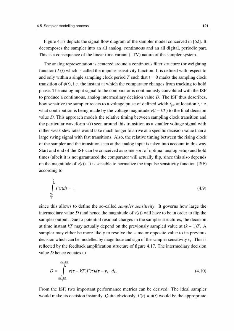
4.5 Sampler modelling process 121
Figure 4.17 depicts the signal flow diagram of the sampler model conceived in [62]. Itdecomposes the sampler into an all analog, continuous and an all digital, periodic part.This is a consequence of the linear time variant (LTV) nature of the sampler system.
The analog representation is centered around a continuous filter structure (or weightingfunction) Γ(t) which is called the impulse sensitivity function. It is defined with respect toand only within a single sampling clock period T such that t = 0 marks the sampling clocktransition of φ(t), i.e. the instant at which the comparator changes from tracking to holdphase. The analog input signal to the comparator is continuously convoluted with the ISFto produce a continuous, analog intermediary decision value D. The ISF thus describes,how sensitive the sampler reacts to a voltage pulse of defined width tpw at location t, i.e.what contribution is being made by the voltage magnitude v(t − kT ) to the final decisionvalue D. This approach models the relative timing between sampling clock transition andthe particular waveform v(t) seen around this transition as a smaller voltage signal withrather weak slew rates would take much longer to arrive at a specific decision value than alarge swing signal with fast transitions. Also, the relative timing between the rising clockof the sampler and the transition seen at the analog input is taken into account in this way.Start and end of the ISF can be conceived as some sort of optimal analog setup and holdtimes (albeit it is not garantueed the comparator will actually flip, since this also dependson the magnitude of v(t)). It is sensible to normalize the impulse sensitivity function (ISF)according to
T2∫
−T2
Γ(t)dt = 1 (4.9)
since this allows to define the so-called sampler sensitivity. It governs how large theintermediary value D (and hence the magnitude of v(t)) will have to be in order to flip thesampler output. Due to potential residual charges in the sampler structures, the decisionat time instant kT may actually depend on the previously sampled value at (k − 1)T . Asampler may either be more likely to resolve the same or opposite value to its previousdecision which can be modelled by magnitude and sign of the sampler sensitivity vs. This isreflected by the feedback amplification structure of figure 4.17. The intermediary decisionvalue D hence equates to
D =
(2k+1)T2∫
(2k−1)T2
v(τ − kT )Γ(τ)dτ + vs · dk−1 (4.10)
From the ISF, two important performance metrics can be derived: The ideal samplerwould make its decision instantly. Quite obviously, Γ(t) = δ(t) would be the appropriate

122 4 Serializer system component modelling
mathematical description in this case, or, in other words: the ISF is simply equivalent toa Dirac function. Since the ISF really models the impulse response of the time varyingsystem, a frequency response and hence a bandwidth can also be associated with it. In thecase of the ideal sampler, this bandwidth would of course be unlimited. Real and well-behaved samplers will, however, be represented by a peaking function of finite maximum,rolling off rather quickly as one moves away from the maximum (compare figure 4.22below). This broadening of the Dirac function in turn leads to a drop in sampling bandwidth.The degree to which the peak broadens therefore represents a good measure of performancefor a sampler and is called the sampling aperture.
In the literature, sampling aperture is often defined as the full width at half maximum ofthe peak. Here, we choose a more rigorous definition and demand that the level is not setat half of the peaks maximum but such, that eighty percent of the total area of the ISF iscovered by the resulting integration interval symmetric around the ISF peak. The maximumof the ISF will not necessarily be located at t = 0 but can be offset by the so-called aperturedelay which is just a consequence of the sampler device voltage thresholds, capacitancesand the time required for the sampling clock signal to fully establish or impede the devicechannel conductances.
The digital part of the model consists of an ideal sample hold stage which producesDn from D. Note, however, that this ideal sampling procedure does not hold the value ofD instantly at tk = kT but needs to capture the convolution of ISF and v(t) until the ISFmagnitude becomes insignificant. As a result, the point in time at which the output of thecomparator actually flips also strongly depends on the analog input voltage magnitude.This is in stark contrast to a digital latch, where clock to output time only changes mildlywith the particular setup time (at least for setup time values decently distant from themetastable region). The second digital stage is an ideal decision stage which produces thesampler output according to
dn =
+1,Dn ≥ 0
−1,Dn < 0(4.11)
The model described above can of course only be of use, if there is an efficient wayto determine the ISF and sensitivity from actual implementations, i.e. if the model trulycaptures real circuit properties. To this end, different procedures have been devised both forsimulation [62] or in modified form even for lab measurements [22]. As the ISF can, viaFourier transformation, be viewed in frequency domain, too, there is also a more advancedtechnique which uses periodic steady state (PSS) analysis in conjunction with PeriodicAC Analysis [27]. Mathematically, this procedure is more difficult to handle but simulatesmagnitudes faster. It is however not suitable for real number models since circuits to beanalzed by PSS may not have hidden states which all kinds of registered values as they
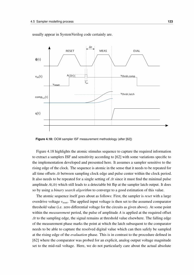
4.5 Sampler modelling process 123
usually appear in SystemVerilog code certainly are.
ϕ(t)
compout(t)
RESET MEAS EVAL
vin(t)
vreset
A(Δt)
Δt
vthrsh,comp
tpw
vthrsh,latch
q(t)
Figure 4.18: OCM sampler ISF measurement methodology (after [62])
Figure 4.18 highlights the atomic stimulus sequence to capture the required informationto extract a samplers ISF and sensitivity according to [62] with some variations specific tothe implementation developed and presented here. It assumes a sampler sensitive to therising edge of the clock. The sequence is atomic in the sense that it needs to be repeated forall time offsets ∆t between sampling clock edge and pulse center within the clock period.It also needs to be repeated for a single setting of ∆t since it must find the minimal pulseamplitude A(∆t) which still leads to a detectable bit flip at the sampler latch output. It doesso by using a binary search algorithm to converge to a good estimation of this value.
The atomic sequence itself goes about as follows: First, the sampler is reset with a largeoverdrive voltage vreset. The applied input voltage is then set to the assumed comparatorthreshold value (i.e. zero differential voltage for the circuits as given above). At some pointwithin the measurement period, the pulse of amplitude A is applied at the required offset∆t to the sampling edge, the signal remains at threshold value elsewhere. The falling edgeof the measurement phase marks the point at which the latch subsequent to the comparatorneeds to be able to capture the resolved digital value which can then safely be sampledat the rising edge of the evaluation phase. This is in contrast to the procedure defined in[62] where the comparator was probed for an explicit, analog output voltage magnitudeset to the mid-rail voltage. Here, we do not particularly care about the actual absolute
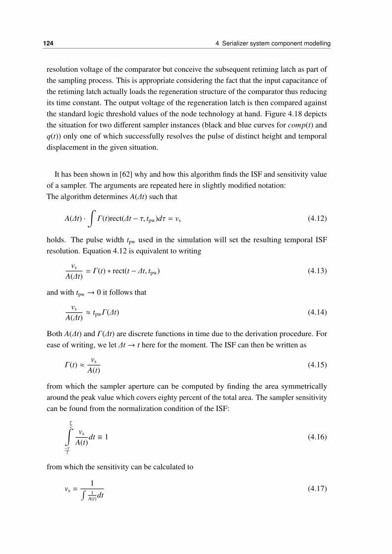
124 4 Serializer system component modelling
resolution voltage of the comparator but conceive the subsequent retiming latch as part ofthe sampling process. This is appropriate considering the fact that the input capacitance ofthe retiming latch actually loads the regeneration structure of the comparator thus reducingits time constant. The output voltage of the regeneration latch is then compared againstthe standard logic threshold values of the node technology at hand. Figure 4.18 depictsthe situation for two different sampler instances (black and blue curves for comp(t) andq(t)) only one of which successfully resolves the pulse of distinct height and temporaldisplacement in the given situation.
It has been shown in [62] why and how this algorithm finds the ISF and sensitivity valueof a sampler. The arguments are repeated here in slightly modified notation:The algorithm determines A(∆t) such that
A(∆t) ·∫Γ(t)rect(∆t − τ, tpw)dτ = vs (4.12)
holds. The pulse width tpw used in the simulation will set the resulting temporal ISFresolution. Equation 4.12 is equivalent to writing
vs
A(∆t)= Γ(t) ∗ rect(t − ∆t, tpw) (4.13)
and with tpw → 0 it follows that
vs
A(∆t)≈ tpwΓ(∆t) (4.14)
Both A(∆t) and Γ(∆t) are discrete functions in time due to the derivation procedure. Forease of writing, we let ∆t → t here for the moment. The ISF can then be written as
Γ(t) ≈vs
A(t)(4.15)
from which the sampler aperture can be computed by finding the area symmetricallyaround the peak value which covers eighty percent of the total area. The sampler sensitivitycan be found from the normalization condition of the ISF:
T2∫
−T2
vs
A(t)dt ≡ 1 (4.16)
from which the sensitivity can be calculated to
vs =1∫1
A(t)dt(4.17)
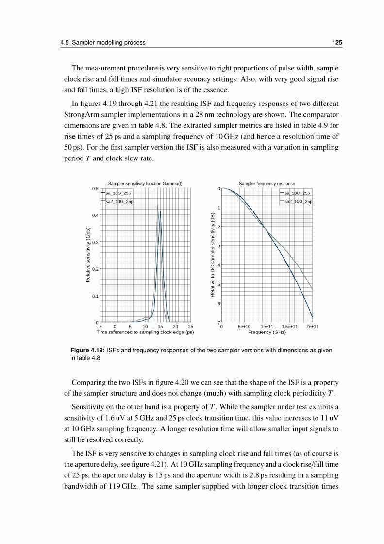
4.5 Sampler modelling process 125
The measurement procedure is very sensitive to right proportions of pulse width, sampleclock rise and fall times and simulator accuracy settings. Also, with very good signal riseand fall times, a high ISF resolution is of the essence.
In figures 4.19 through 4.21 the resulting ISF and frequency responses of two differentStrongArm sampler implementations in a 28 nm technology are shown. The comparatordimensions are given in table 4.8. The extracted sampler metrics are listed in table 4.9 forrise times of 25 ps and a sampling frequency of 10 GHz (and hence a resolution time of50 ps). For the first sampler version the ISF is also measured with a variation in samplingperiod T and clock slew rate.
-5 0 5 10 15 20 250
0.1
0.2
0.3
0.4
0.5
Time referenced to sampling clock edge (ps)
Rel
ativ
e se
nsiti
vity
(1/
ps)
sa_10G_25p
sa2_10G_25p
0 5e+10 1e+11 1.5e+11 2e+11-7
-6
-5
-4
-3
-2
-1
0
Frequency (GHz)
Rel
ativ
e to
DC
sam
pler
sen
sitiv
ity (
dB)
sa_10G_25p
sa2_10G_25p
Sampler sensitivity function Gamma(t) Sampler frequency response
Figure 4.19: ISFs and frequency responses of the two sampler versions with dimensions as givenin table 4.8
Comparing the two ISFs in figure 4.20 we can see that the shape of the ISF is a propertyof the sampler structure and does not change (much) with sampling clock periodicity T .
Sensitivity on the other hand is a property of T . While the sampler under test exhibits asensitivity of 1.6 uV at 5 GHz and 25 ps clock transition time, this value increases to 11 uVat 10 GHz sampling frequency. A longer resolution time will allow smaller input signals tostill be resolved correctly.
The ISF is very sensitive to changes in sampling clock rise and fall times (as of course isthe aperture delay, see figure 4.21). At 10 GHz sampling frequency and a clock rise/fall timeof 25 ps, the aperture delay is 15 ps and the aperture width is 2.8 ps resulting in a samplingbandwidth of 119 GHz. The same sampler supplied with longer clock transition times
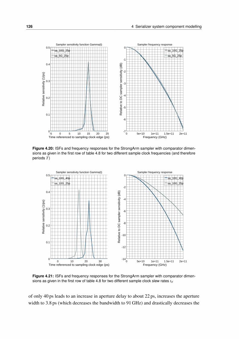
126 4 Serializer system component modelling
-5 0 5 10 15 20 250
0.1
0.2
0.3
0.4
0.5
Time referenced to sampling clock edge (ps)
Rel
ativ
e se
nsiti
vity
(1/
ps)
sa_10G_25p
sa_5G_25p
0 5e+10 1e+11 1.5e+11 2e+11-7
-6
-5
-4
-3
-2
-1
0
Frequency (GHz)
Rel
ativ
e to
DC
sam
pler
sen
sitiv
ity (
dB)
sa_10G_25p
sa_5G_25p
Sampler sensitivity function Gamma(t) Sampler frequency response
Figure 4.20: ISFs and frequency responses for the StrongArm sampler with comparator dimen-sions as given in the first row of table 4.8 for two different sample clock frequencies (and thereforeperiods T )
0 10 20 300
0.1
0.2
0.3
0.4
0.5
Time referenced to sampling clock edge (ps)
Rel
ativ
e se
nsiti
vity
(1/
ps)
sa_10G_40p
sa_10G_25p
0 5e+10 1e+11 1.5e+11 2e+11-14
-12
-10
-8
-6
-4
-2
0
Frequency (GHz)
Rel
ativ
e to
DC
sam
pler
sen
sitiv
ity (
dB)
sa_10G_40p
sa_10G_25p
Sampler sensitivity function Gamma(t) Sampler frequency response
Figure 4.21: ISFs and frequency responses for the StrongArm sampler with comparator dimen-sions as given in the first row of table 4.8 for two different sample clock slew rates trf
of only 40 ps leads to an increase in aperture delay to about 22 ps, increases the aperturewidth to 3.8 ps (which decreases the bandwidth to 91 GHz) and drastically decreases the
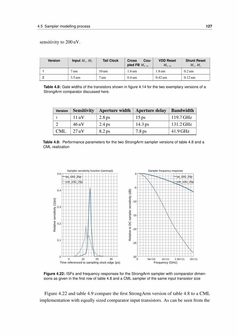
4.5 Sampler modelling process 127
sensitivity to 200 uV.
Version Input M1, M2 Tail Clock Cross Cou-pled FB Mn−m
VDD ResetMn−m
Shunt ResetMx, My
1 7 um 10 um 1.6 um 1.8 um 0.2 um
2 3.5 um 7 um 0.4 um 0.42 um 0.12 um
Table 4.8: Gate widths of the transistors shown in figure 4.14 for the two exemplary versions of aStrongArm comparator discussed here.
Version Sensitivity Aperture width Aperture delay Bandwidth1 11 uV 2.8 ps 15 ps 119.7 GHz2 46 uV 2.4 ps 14.3 ps 131.2 GHzCML 27 uV 8.2 ps 7.8 ps 41.9 GHz
Table 4.9: Performance parameters for the two StrongArm sampler versions of table 4.8 and aCML realization
0 10 20 300
0.1
0.2
0.3
0.4
0.5
Time referenced to sampling clock edge (ps)
Rel
ativ
e se
nsiti
vity
(1/
ps)
sa_10G_25p
cml_10G_25p
0 5e+10 1e+11 1.5e+11 2e+11-30
-25
-20
-15
-10
-5
0
Frequency (GHz)
Rel
ativ
e to
DC
sam
pler
sen
sitiv
ity (
dB)
sa_10G_25p
cml_10G_25p
Sampler sensitivity function Gamma(t) Sampler frequency response
Figure 4.22: ISFs and frequency responses for the StrongArm sampler with comparator dimen-sions as given in the first row of table 4.8 and a CML sampler of the same input transistor size
Figure 4.22 and table 4.9 compare the first StrongArm version of table 4.8 to a CMLimplementation with equally sized comparator input transistors. As can be seen from the

128 4 Serializer system component modelling
graphs, the aperture width of the CML implementation is much wider which leads to adrastic decrease in sampling bandwidth. The sensitivity on the other hand maintains avery good level of 27 uV and its aperture delay is significantly lower compared to theStrongArm version.
Therefore, in addition to the advantages and disadvantages of the two implementationsas described above, the measurements indicate the very small aperture width (and thereforehigh bandwidth) and good sensitivity as further strong points of StrongArm based samplerscompared to their CML counterparts whereas CML versions have an additional benefit inproviding small aperture delays.
As one can see from figure 4.19 almost the same ISF shape and therefore aperture widthcan be realized with smaller or larger devices within the comparator. Why then would adesigner still opt for the larger version of a sampler? It seems more benefitial to use verysmall devices with fast clock slew rates if the sampler sensitivity is of much concern. Afterall, a large device will certainly produce more clock load and higher transient currents!One reason is that device mismatches drastically increase with smaller device sizes andmore static offset correction would then be needed - an effect that becomes more severewith more advanced technology nodes. Perhaps the more important answer however lies inthe intrinsic noise properties of the sampler.
Intrinsic noise analysis First, it is rather difficult to find a good estimate of sampler noisefrom analytic calculations. Especially in the case of a StrongArm comparator there is asubstantial amount of device noise sources to be considered. Next, for a very nonlineardevice such as a sampler or latch, there is no direct way to refer the noise seen at its full railoutputs back to a representative noise magnitude at its inputs - the so called input referrednoise. However, for serializer link budgeting we ultimately require a metric value whichallows to calculate the impact of sampler intrinsic noise on the estimated eye diagram seenby the receivers sampler inputs. Furthermore, a good portion of the overall noise level willresult from periodic and thus deterministic effects, most notably the clock feedthrough.This is also called cyclostationary noise and cannot be covered by small signal models.
There has been a procedure suggested in [54] and extended by [57] to find the inputreferred noise σn,samp of a sampler. It is based on a transient simulation with all intrinsicnoise sources of all components within the sampler activated. Since the sampler designis rather small, a single simulation run is still fast enough to cover several hundreds ofnanoseconds. This can be done even when choosing the noise bandwidth of the transient,noise enhanced simulation to be rather large. As the lower bandwidth limit also sets alimit on minimum simulation time, this value needs to be chosen with respect to run timerather than by physical indication, i.e. in the range of some MHz. This will then of coursenot capture the steeply rising 1/ f noise components of the devices. However, since theupper bound will be chosen in accordance with the samplers bandwidth as obtained from
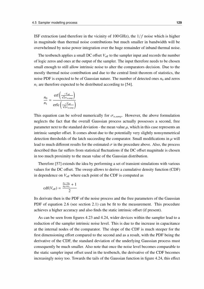
4.5 Sampler modelling process 129
ISF extraction (and therefore in the vicinity of 100 GHz), the 1/ f noise which is higherin magnitude than thermal noise contributions but much smaller in bandwidth will beoverwhelmed by noise power integration over the huge remainder of inband thermal noise.
The testbench applies a small DC offset Voff to the sampler input and records the numberof logic zeros and ones at the output of the sampler. The input therefore needs to be chosensmall enough to still allow intrinsic noise to alter the comparators decision. Due to themostly thermal noise contribution and due to the central limit theorem of statistics, thenoise PDF is expected to be of Gaussian nature. The number of detected ones n0 and zerosn1 are therefore expected to be distributed according to [54].
n0
n1=
erf(−Voff√2σn,samp
)erfc
(−Voff√2σn,samp
)This equation can be solved numerically for σn,samp. However, the above formulationneglects the fact that the overall Gaussian process actually possesses a second, freeparameter next to the standard deviation - the mean value µ, which in this case represents anintrinsic sampler offset. It comes about due to the potentially very slightly nonsymmetricaldetection thresholds of the latch succeeding the comparator. Small modifications in µ willlead to much different results for the estimated σ in the procedure above. Also, the processdescribed thus far suffers from statistical fluctuations if the DC offset magnitude is chosenin too much proximity to the mean value of the Gaussian distribution.
Therefore [57] extends the idea by performing a set of transient simulations with variousvalues for the DC offset. The sweep allows to derive a cumulative density function (CDF)in dependence on Voff where each point of the CDF is computed as
cdf(Voff) =n1−n0n0+n1+ 1
2
Its derivate then is the PDF of the noise process and the free parameters of the GaussianPDF of equation 2.6 (see section 2.1) can be fit to the measurement. This procedureachieves a higher accuracy and also finds the static intrinsic offset (if present).
As can be seen from figures 4.23 and 4.24, wider devices within the sampler lead to areduction of the sampler intrinsic noise level. This is due to the increase in capacitanceat the internal nodes of the comparator. The slope of the CDF is much steeper for thefirst dimensioning effort compared to the second and as a result, with the PDF being thederivative of the CDF, the standard deviation of the underlying Gaussian process mustconsequently be much smaller. Also note that once the noise level becomes comparable tothe static sampler input offset used in the testbench, the derivative of the CDF becomesincreasingly noisy too. Towards the tails of the Gaussian function in figure 4.24, this effect
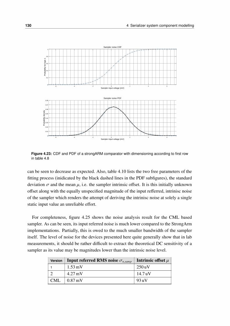
130 4 Serializer system component modelling
-6 -4 -2 0 2 4 60
0.2
0.4
0.6
0.8
1
Sampler input voltage (mV)
Pro
babi
lity
for
logi
c 1
-6 -4 -2 0 2 4 60
0.01
0.02
0.03
0.04
0.05
0.06
0.07
0.08
Sampler input voltage (mV)
Pro
babi
lity
dens
ity
Sampler noise CDF
Sampler noise PDF
Figure 4.23: CDF and PDF of a strongARM comparator with dimensioning according to first rowin table 4.8
can be seen to decrease as expected. Also, table 4.10 lists the two free parameters of thefitting process (inidicated by the black dashed lines in the PDF subfigures), the standarddeviation σ and the mean µ, i.e. the sampler intrinsic offset. It is this initially unknownoffset along with the equally unspecified magnitude of the input refferred, intrinisc noiseof the sampler which renders the attempt of deriving the intrinisc noise at solely a singlestatic input value an unreliable effort.
For completeness, figure 4.25 shows the noise analysis result for the CML basedsampler. As can be seen, its input referred noise is much lower compared to the StrongArmimplementations. Partially, this is owed to the much smaller bandwidth of the sampleritself. The level of noise for the devices presented here quite generally show that in labmeasurements, it should be rather difficult to extract the theoretical DC sensitivity of asampler as its value may be magnitudes lower than the intrinsic noise level.
Version Input referred RMS noise σn,samp Intrinsic offset µ1 1.53 mV 250 uV2 4.27 mV 14.7 uVCML 0.87 mV 93 uV
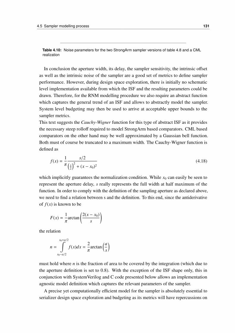
4.5 Sampler modelling process 131
Table 4.10: Noise parameters for the two StrongArm sampler versions of table 4.8 and a CMLrealization
In conclusion the aperture width, its delay, the sampler sensitivity, the intrinsic offsetas well as the intrinsic noise of the sampler are a good set of metrics to define samplerperformance. However, during design space exploration, there is initially no schematiclevel implementation available from which the ISF and the resulting parameters could bedrawn. Therefore, for the RNM modelling procedure we also require an abstract functionwhich captures the general trend of an ISF and allows to abstractly model the sampler.System level budgeting may then be used to arrive at acceptable upper bounds to thesampler metrics.This text suggests the Cauchy-Wigner function for this type of abstract ISF as it providesthe necessary steep rolloff required to model StrongArm based comparators. CML basedcomparators on the other hand may be well approximated by a Gaussian bell function.Both must of course be truncated to a maximum width. The Cauchy-Wigner function isdefined as
f (x) =1π
s/2(s2
)2+ (x − x0)2
(4.18)
which implicitly guarantees the normalization condition. While x0 can easily be seen torepresent the aperture delay, s really represents the full width at half maximum of thefunction. In order to comply with the definition of the sampling aperture as declared above,we need to find a relation between s and the definition. To this end, since the antiderivativeof f (x) is known to be
F(x) =1π
arctan(2(x − x0)
s
)the relation
n =
x0+a/2∫x0−a/2
f (x)dx =2π
arctan(a
s
)
must hold where n is the fraction of area to be covered by the integration (which due tothe aperture definition is set to 0.8). With the exception of the ISF shape only, this inconjunction with SystemVerilog and C code presented below allows an implementationagnostic model definition which captures the relevant parameters of the sampler.
A precise yet computationally efficient model for the sampler is absolutely essential toserializer design space exploration and budgeting as its metrics will have repercussions on
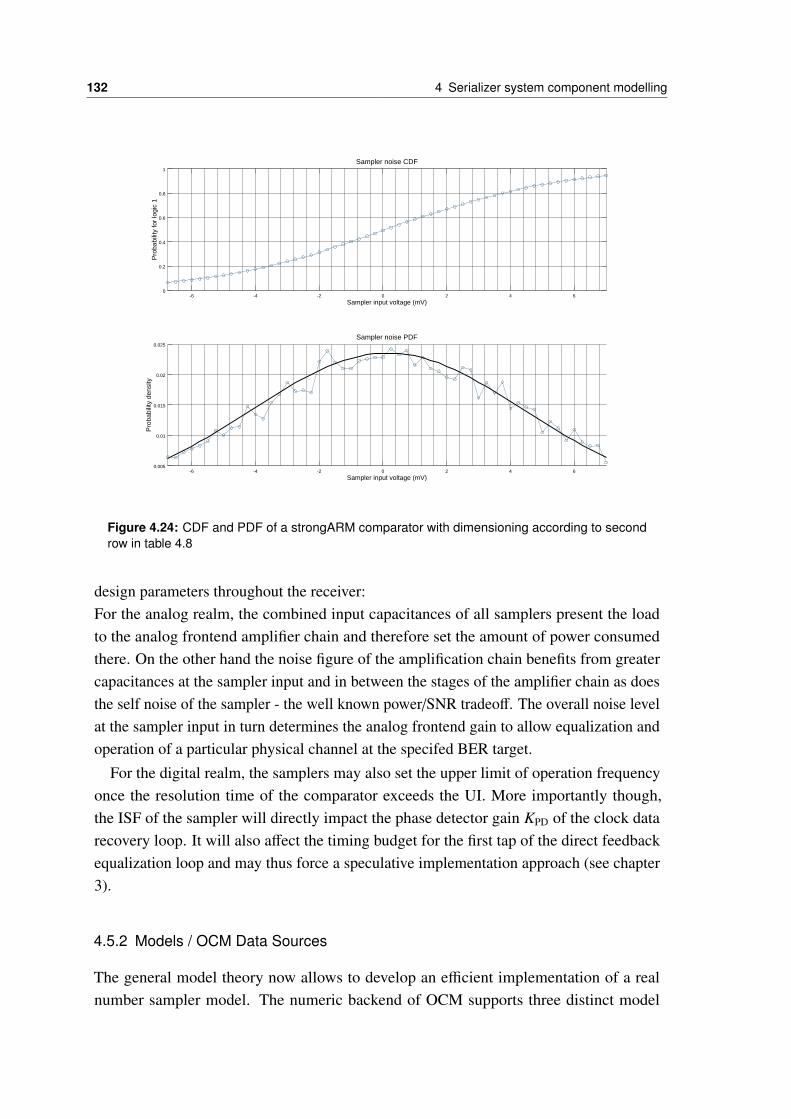
132 4 Serializer system component modelling
-6 -4 -2 0 2 4 60
0.2
0.4
0.6
0.8
1
Sampler input voltage (mV)
Pro
babi
lity
for
logi
c 1
-6 -4 -2 0 2 4 60.005
0.01
0.015
0.02
0.025
Sampler input voltage (mV)
Pro
babi
lity
dens
ity
Sampler noise CDF
Sampler noise PDF
Figure 4.24: CDF and PDF of a strongARM comparator with dimensioning according to secondrow in table 4.8
design parameters throughout the receiver:For the analog realm, the combined input capacitances of all samplers present the loadto the analog frontend amplifier chain and therefore set the amount of power consumedthere. On the other hand the noise figure of the amplification chain benefits from greatercapacitances at the sampler input and in between the stages of the amplifier chain as doesthe self noise of the sampler - the well known power/SNR tradeoff. The overall noise levelat the sampler input in turn determines the analog frontend gain to allow equalization andoperation of a particular physical channel at the specifed BER target.
For the digital realm, the samplers may also set the upper limit of operation frequencyonce the resolution time of the comparator exceeds the UI. More importantly though,the ISF of the sampler will directly impact the phase detector gain KPD of the clock datarecovery loop. It will also affect the timing budget for the first tap of the direct feedbackequalization loop and may thus force a speculative implementation approach (see chapter3).
4.5.2 Models / OCM Data Sources
The general model theory now allows to develop an efficient implementation of a realnumber sampler model. The numeric backend of OCM supports three distinct model
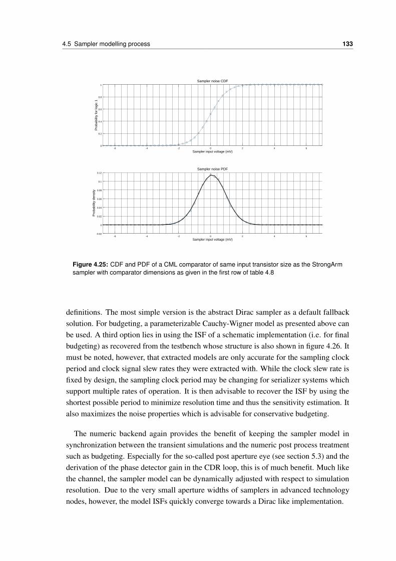
4.5 Sampler modelling process 133
-6 -4 -2 0 2 4 60
0.2
0.4
0.6
0.8
1
Sampler input voltage (mV)
Pro
babi
lity
for
logi
c 1
-6 -4 -2 0 2 4 6-0.02
0
0.02
0.04
0.06
0.08
0.1
0.12
Sampler input voltage (mV)
Pro
babi
lity
dens
ity
Sampler noise CDF
Sampler noise PDF
Figure 4.25: CDF and PDF of a CML comparator of same input transistor size as the StrongArmsampler with comparator dimensions as given in the first row of table 4.8
definitions. The most simple version is the abstract Dirac sampler as a default fallbacksolution. For budgeting, a parameterizable Cauchy-Wigner model as presented above canbe used. A third option lies in using the ISF of a schematic implementation (i.e. for finalbudgeting) as recovered from the testbench whose structure is also shown in figure 4.26. Itmust be noted, however, that extracted models are only accurate for the sampling clockperiod and clock signal slew rates they were extracted with. While the clock slew rate isfixed by design, the sampling clock period may be changing for serializer systems whichsupport multiple rates of operation. It is then advisable to recover the ISF by using theshortest possible period to minimize resolution time and thus the sensitivity estimation. Italso maximizes the noise properties which is advisable for conservative budgeting.
The numeric backend again provides the benefit of keeping the sampler model insynchronization between the transient simulations and the numeric post process treatmentsuch as budgeting. Especially for the so-called post aperture eye (see section 5.3) and thederivation of the phase detector gain in the CDR loop, this is of much benefit. Much likethe channel, the sampler model can be dynamically adjusted with respect to simulationresolution. Due to the very small aperture widths of samplers in advanced technologynodes, however, the model ISFs quickly converge towards a Dirac like implementation.

134 4 Serializer system component modelling
Optimized C Reorderingand convolution
Data preparationComputation of
Impulse sensitivity function
Stimulus GenerationInput and Output monitoring
with OCM routine
OCM Post Processing
compare / verify
DUT - Sampler (Model)
SystemVerilogOCM Sampler Module
Model fileas recorded by this TB
from schematic implementation
Cauchy-Lorenz ModelAperture, Sensitivity,
Delay, Offset
Model definition
Sampler metrics
SystemVerilog Realm
OCM C RealmOCM Octave Realm
input stream and
trigger indexbinary
decisionParameters
Impulse SensitivityFunction
Aperture, ...,Sensitivity
or
Figure 4.26: OCM sampler modelling and testbench flow
4.5.3 SystemVerilog considerations
The SystemVerilog module of the sampler continuously records the stream of real numbervalues which represent the voltage difference seen at the sampler input. The depth ofthe history it records spans an adjustable integer multiple of the sampler aperture widthcommonly set to three. Generally, it would be possible to also continuously convolutethe input data with the FIR-like filter defined by the ISF. However, in contrast to thechannel module, there may be quite a number of sampler instances in a given realizationof a receiver. The design presented in chapter 6 requires a total of fourteen samplerinstances. Continuous convolution in all these instances in order to obtain just a singlevalue per period would certainly consume a lot of computing resource without any apparentbenefit. Therefore, the sampling module calls its DPI convolution function only oncewhen triggered by its clock input. Since the ISF may span to either side of the triggerinstant, the history will be recorded even after the trigger event occured until the specifiedinteger multiple of the ISF aperture is fully recorded. Even though the convolution functionreturns with its binary decision within the same time slot of the simulator, this introducesadditional delay in the clock to output characteristic of the comparator. Since the samplerstructure always consists of a comparator element whose output is retimed by at least asingle latch stage, this does not pose a problem if the post trigger history item count doesnot exceed the resolution time of half the sampling period.
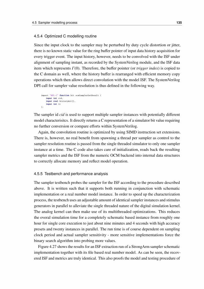
4.5 Sampler modelling process 135
4.5.4 Optimized C modelling routine
Since the input clock to the sampler may be perturbed by duty cycle distortion or jitter,there is no known static value for the ring buffer pointer of input data history acquisition forevery trigger event. The input history, however, needs to be convolved with the ISF underalignment of sampling instant, as recorded by the SystemVerilog module, and the ISF dataitem which represents Γ(0). Therefore, the buffer pointer (or trigger index) is copied tothe C domain as well, where the history buffer is rearranged with efficient memory copyoperations which then allows direct convolution with the model ISF. The SystemVerilogDPI call for sampler value resolution is thus defined in the following way.
import "DPI-C" function bit ocmSamplerGetResult (
input int cid,
input real historyArr[],
input int ti
);
The sampler id cid is used to support multiple sampler instances with potentially differentmodel characterisitcs. It directly returns a C representation of a simulator bit value requiringno further conversion or compare efforts within SystemVerilog.
Again, the convolution routine is optimized by using SIMD instruction set extensions.There is, however, no real benefit from spawning a thread per sampler as control to thesampler resolution routine is passed from the single threaded simulator to only one samplerinstance at a time. The C code also takes care of initialization, reads back the resultingsampler metrics and the ISF from the numeric OCM backend into internal data structuresto correctly allocate memory and reflect model operation.
4.5.5 Testbench and performance analysis
The sampler testbench probes the sampler for the ISF according to the procedure describedabove. It is written such that it supports both running in conjunction with schematicimplementation or a real number model instance. In order to speed up the characterizationprocess, the testbench uses an adjustable amount of identical sampler instances and stimulusgenerators in parallel to alleviate the single threaded nature of the digital simulation kernel.The analog kernel can then make use of its multithreaded optimizations. This reducesthe overal simulation time for a completely schematic based instance from roughly onehour for single core execution to just about nine minutes and 4 seconds with high accuracypresets and twenty instances in parallel. The run time is of course dependent on samplingclock period and actual sampler sensitivity - more sensitive implementations force thebinary search algorithm into probing more values.
Figure 4.27 shows the results for an ISF extraction run of a StrongArm sampler schematicimplementation together with its file based real number model. As can be seen, the recov-ered ISF and metrics are truly identical. This also proofs the model and testing procedure of
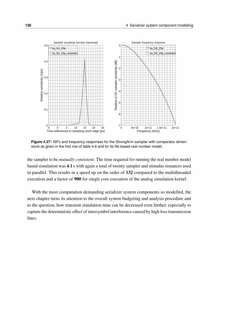
136 4 Serializer system component modelling
-5 0 5 10 15 20 250
0.1
0.2
0.3
0.4
0.5
Time referenced to sampling clock edge (ps)
Rel
ativ
e se
nsiti
vity
(1/
ps)
sa_5G_25p
sa_5G_25p_modelled
0 5e+10 1e+11 1.5e+11 2e+11-7
-6
-5
-4
-3
-2
-1
0
Frequency (GHz)
Rel
ativ
e to
DC
sam
pler
sen
sitiv
ity (
dB)
sa_5G_25p
sa_5G_25p_modelled
Sampler sensitivity function Gamma(t) Sampler frequency response
Figure 4.27: ISFs and frequency responses for the StrongArm sampler with comparator dimen-sions as given in the first row of table 4.8 and for its file based real number model.
the sampler to be mutually consistent. The time required for running the real number modelbased simulation was 4.1 s with again a total of twenty sampler and stimulus instances usedin parallel. This results in a speed up on the order of 132 compared to the multithreadedexecution and a factor of 900 for single core execution of the analog simulation kernel.
With the most computation demanding serializer system components so modelled, thenext chapter turns its attention to the overall system budgeting and analysis procedure andto the question, how transient simulation time can be decreased even further, especially tocapture the deterministic effect of intersymbol interference caused by high loss transmissionlines.
5 Link budgeting
Since the advent of multi-gigabit, baseband communication channels about two decadesago, several techniques have been developed to assist in the design of these systems andtheir constituent subcomponents. As discussed in chapters 2 and 4, each subsystem has aset of performance metrics. They may each have a more or less subtle impact on one ormore toplevel system metrics, either directly or by interaction with other subcomponentproperties. An obvious example of this may be the voltage noise spectral density S vv,pdn ofthe PDN which impacts the noise level seen at the receiver samplers via the various powersupply rejection ratios of the receiver amplifier stages. It is a simple example of how onesubcomponent metric cannot be utilized or constrained in a meaningful manner withoutknowing and constraining another subcomponents metric.
It is the central task of the link budgeting procedure to establish the relations between allimportant subcomponent metrics (if they exist) and their combined or isolated impact onkey system performance metrics. For the above mentioned example, the affected toplevelmetric of S vv,pdn and the PSRR would of course be the eye height or the expected BERof the system itself. Once these relations are established, budgeting helps to identify thestrongest contributors to system performance degradation. Some of these metrics, however,may be subject to other constraints such as power consumption in which case other, relatedmetrics have to be improved in its stead.
The goal here is to develop an approach for the openMGT/OCM framework whichallows to budget a system as described in chapter 2 without resorting to third partytools and parameter synchronization. To that end, the algorithms found in the paperspresented here will be adapted and modified as needed. In order to make this processcomprehensible, the ideas and steps taken from the papers will be repeated here albeit withadapted nomenclature and mathematical convention for improved consistency, especiallywith the peak distortion analysis (PDA) algorithm of section 5.2. The starting point ofalmost every approach is the physical transmission channel itself as its impact on requiredsystem components and their metrics is by far the strongest. The influence of voltage noisesources such as the power supply noise and the thermal noise of the circuit elements iswell understood and can be treated independently of the transmitted signal. This is due tothe linear time invariance of the TX FIR filter, the channel and the RX CTLE structure.Special care must only be taken with the CDR circuit (see section 5.3.6 ) as voltage noisewill impact key design parameters of this subcomponent and cause nonlinear backaction
137
138 5 Link budgeting
on the subcomponents behavior. The central question of budgeting therefore is, how jittersources in the system are being dealt with in the presence of high loss transmission linesand linear equalization efforts.
5.1 History and state of the art
Let H( jω) be the frequency transfer function of the transmission channel terminatedat transmitter and receiver. Its impulse response h(t) can be found as usual by Fouriertransformation. The channel response to an arbitrary input waveform x(t) can then becomputed by convolution to
y(t) = h(t) ∗ x(t) =
∞∫−∞
h(t)x(t − dτ)dτ
Further, let ε(t) represent the instantaneous time interval error of x(t) (see section 2.2.1).This of course only makes sense, if x(t) has a fundamental periodicity T . As x(t) is thecontinuous time representation of a stream of digital bits, this periodicity T is given by theunit interval of a bit. As mentioned in section 2.1, x(t) can be rewritten as
x(t) =1
2π
∞∫−∞
X(ω)e jωtdω
and thus
x( t + ε(t) ) =1
2π
∞∫−∞
(X(ω)e jωε(t)
)e jωtdω
As expected, the Fourier transform would lead to a completely new set of coefficientsX(ω) = X(ω)e jωε(t). However, if the condition |ε(t)| T holds, i.e. the time interval errorsremain small compared to the unit bit interval, X(ω) can be Taylor expanded:
x(t + ε(t)) =1
2π
∞∫−∞
(X(ω)e jωε(t)
)e jωtdω
=1
2π
∞∫−∞
(X(ω)e jωt
(1 + jωε(t) −
ω2ε2(t)2
+jω3ε3(t)
6+ ...
)dω
= x(t) + ε(t)dx(t)
dt+ε2(t)
2d2x(t)
dt2 + ...
(5.1)
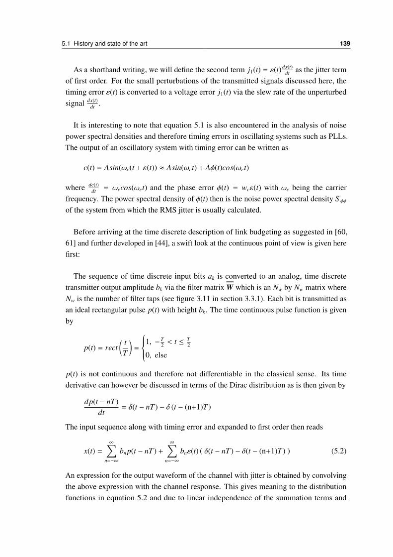
5.1 History and state of the art 139
As a shorthand writing, we will define the second term j1(t) = ε(t) dx(t)dt as the jitter term
of first order. For the small perturbations of the transmitted signals discussed here, thetiming error ε(t) is converted to a voltage error j1(t) via the slew rate of the unperturbedsignal dx(t)
dt .
It is interesting to note that equation 5.1 is also encountered in the analysis of noisepower spectral densities and therefore timing errors in oscillating systems such as PLLs.The output of an oscillatory system with timing error can be written as
c(t) = Asin(ωc(t + ε(t)) ≈ Asin(ωct) + Aφ(t)cos(ωct)
where dc(t)dt = ωccos(ωct) and the phase error φ(t) = wcε(t) with ωc being the carrier
frequency. The power spectral density of φ(t) then is the noise power spectral density S φφof the system from which the RMS jitter is usually calculated.
Before arriving at the time discrete description of link budgeting as suggested in [60,61] and further developed in [44], a swift look at the continuous point of view is given herefirst:
The sequence of time discrete input bits ak is converted to an analog, time discretetransmitter output amplitude bk via the filter matrix W which is an Nw by Nw matrix whereNw is the number of filter taps (see figure 3.11 in section 3.3.1). Each bit is transmitted asan ideal rectangular pulse p(t) with height bk. The time continuous pulse function is givenby
p(t) = rect( tT
)=
1, −T2 < t ≤ T
2
0, else
p(t) is not continuous and therefore not differentiable in the classical sense. Its timederivative can however be discussed in terms of the Dirac distribution as is then given by
dp(t − nT )dt
= δ(t − nT ) − δ (t − (n+1)T )
The input sequence along with timing error and expanded to first order then reads
x(t) =∞∑
n=−∞
bn p(t − nT ) +∞∑
n=−∞
bnε(t) ( δ(t − nT ) − δ(t − (n+1)T ) ) (5.2)
An expression for the output waveform of the channel with jitter is obtained by convolvingthe above expression with the channel response. This gives meaning to the distributionfunctions in equation 5.2 and due to linear independence of the summation terms and
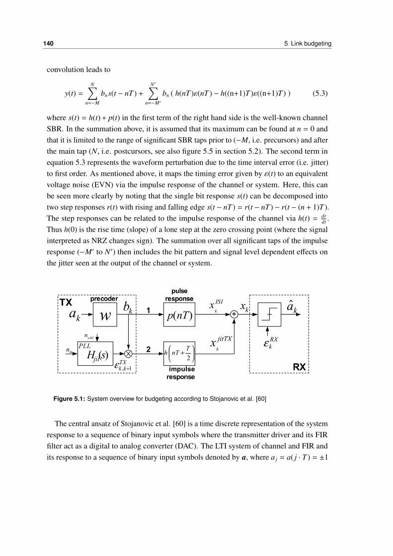
140 5 Link budgeting
convolution leads to
y(t) =N∑
n=−M
bns(t − nT ) +N′∑
n=−M′bn ( h(nT )ε(nT ) − h((n+1)T )ε((n+1)T ) ) (5.3)
where s(t) = h(t) ∗ p(t) in the first term of the right hand side is the well-known channelSBR. In the summation above, it is assumed that its maximum can be found at n = 0 andthat it is limited to the range of significant SBR taps prior to (−M, i.e. precursors) and afterthe main tap (N, i.e. postcursors, see also figure 5.5 in section 5.2). The second term inequation 5.3 represents the waveform perturbation due to the time interval error (i.e. jitter)to first order. As mentioned above, it maps the timing error given by ε(t) to an equivalentvoltage noise (EVN) via the impulse response of the channel or system. Here, this canbe seen more clearly by noting that the single bit response s(t) can be decomposed intotwo step responses r(t) with rising and falling edge s(t − nT ) = r(t − nT ) − r(t − (n + 1)T ).The step responses can be related to the impulse response of the channel via h(t) = dr
dt .Thus h(0) is the rise time (slope) of a lone step at the zero crossing point (where the signalinterpreted as NRZ changes sign). The summation over all significant taps of the impulseresponse (−M′ to N′) then includes the bit pattern and signal level dependent effects onthe jitter seen at the output of the channel or system.
Figure 5.1: System overview for budgeting according to Stojanovic et al. [60]
The central ansatz of Stojanovic et al. [60] is a time discrete representation of the systemresponse to a sequence of binary input symbols where the transmitter driver and its FIRfilter act as a digital to analog converter (DAC). The LTI system of channel and FIR andits response to a sequence of binary input symbols denoted by a, where a j = a( j · T ) = ±1
5.1 History and state of the art 141
can be written as
ytotal(t) =N∑
j=−M
b js(εtx, j − jT )
where again the binary input symbols a j are encoded to analog output amplitudes b j =
b( j · T ) via the coding matrix W. The output driver retimes the transmitted symbols to itslocal PLL reference clock which has a timing error function εtx(t) and where the transitionto the time discrete description is again made by setting εtx,j = εtx( jT ). There is no timingerror accumulation taking place in the transmitter, therefore only the particular timing errorεtx, j at the nominal time instant jT is important here. At time instant t = mT + εrx,m thereceiver samples the incoming data with its jittered clock. The time discrete sequence canthen be written as
ytotal,m =
N∑j=−M
b js(εtx, j + εrx, j − (m − j)T ) (5.4)
It can be decomposed into an ISI impaired signal and noise components. The noisecomponents are due to TX jitter εT X and RX jitter εRX and are obtained by first order Taylorexpansion of equation 5.4. This leads to the so-called EVN representation of jitter at thereceiver sampler:
ytotal,m = yisi,m + ytxn,m + yrxn,m (5.5)
yisi,m =
N∑j=−M
bm− js j (5.6)
ytxn,m =
N∑j=−M
bm− j
(h j−1εtx,m− j+1 − h jεtx,m− j
)(5.7)
yrxn,m = εrx,m
N∑j=−M
bm− j
(h j − h j−1
)(5.8)
where sn = s(nT ) and hn = h(nT +T/2). Note that here ytxn,m and yrxn,m are the time discreterepresentation of j1(t), the jitter term of first order as also found in equation 5.1. TheFIR filter and channel will take an effect on how transmitter jitter appears at the samplerwhile receiver jitter will only be scaled by a factor. Spectrally speaking, the transmit jitterexperiences a coloring (filtering) process which is due to the channel frequency responseand the FIR precoding efforts. Scaling of receiver jitter on the other hand is essentiallygiven by the specific slew rate of the signal incident at the receiver. The interaction betweenslew rate and jitter can be illustrated more clearly by turning to a specific use case of theabove formulas:
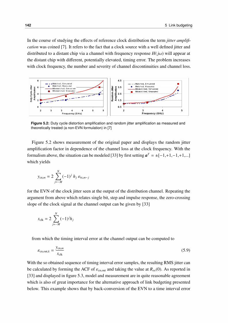
142 5 Link budgeting
In the course of studying the effects of reference clock distribution the term jitter amplifi-cation was coined [7]. It refers to the fact that a clock source with a well defined jitter anddistributed to a distant chip via a channel with frequency response H( jω) will appear atthe distant chip with different, potentially elevated, timing error. The problem increaseswith clock frequency, the number and severity of channel discontinuities and channel loss.
Figure 5.2: Duty cycle distortion amplification and random jitter amplification as measured andtheoretically treated (a non-EVN formulation) in [7]
Figure 5.2 shows measurement of the original paper and displays the random jitteramplification factor in dependence of the channel loss at the clock frequency. With theformalism above, the situation can be modeled [33] by first setting aT = ±[−1,+1,−1,+1,...]which yields
ycn,m = 2N∑
j=−M
(−1) j h j εtx,m− j
for the EVN of the clock jitter seen at the output of the distribution channel. Repeating theargument from above which relates single bit, step and impulse response, the zero-crossingslope of the clock signal at the channel output can be given by [33]
sclk = 2N∑
j=−M
(−1) jh j
from which the timing interval error at the channel output can be computed to
εcn,out,k =ycn,m
sclk(5.9)
With the so obtained sequence of timing interval error samples, the resulting RMS jitter canbe calculated by forming the ACF of εcn,out and taking the value at Rεε(0). As reported in[33] and displayed in figure 5.3, model and measurement are in quite reasonable agreementwhich is also of great importance for the alternative approach of link budgeting presentedbelow. This example shows that by back-conversion of the EVN to a time interval error
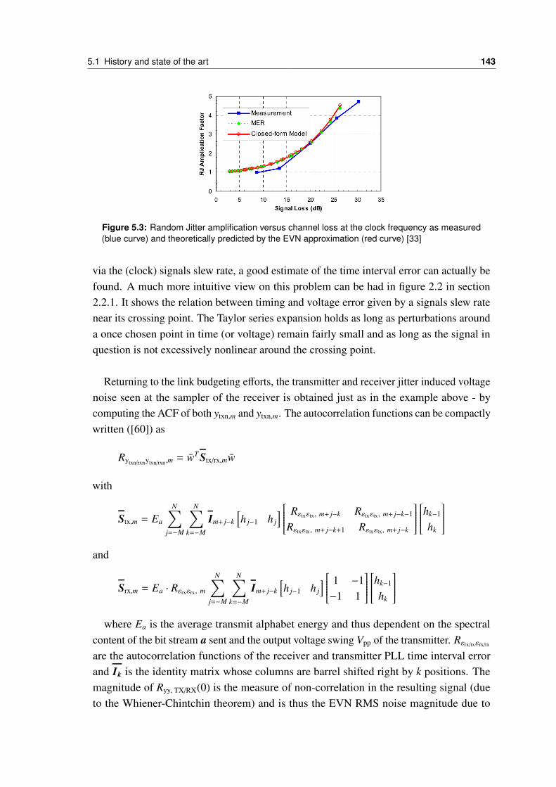
5.1 History and state of the art 143
Figure 5.3: Random Jitter amplification versus channel loss at the clock frequency as measured(blue curve) and theoretically predicted by the EVN approximation (red curve) [33]
via the (clock) signals slew rate, a good estimate of the time interval error can actually befound. A much more intuitive view on this problem can be had in figure 2.2 in section2.2.1. It shows the relation between timing and voltage error given by a signals slew ratenear its crossing point. The Taylor series expansion holds as long as perturbations arounda once chosen point in time (or voltage) remain fairly small and as long as the signal inquestion is not excessively nonlinear around the crossing point.
Returning to the link budgeting efforts, the transmitter and receiver jitter induced voltagenoise seen at the sampler of the receiver is obtained just as in the example above - bycomputing the ACF of both ytxn,m and ytxn,m. The autocorrelation functions can be compactlywritten ([60]) as
Rytxn/rxnytxn/rxn,m = wT Stx/rx,mw
with
Stx,m = Ea
N∑j=−M
N∑k=−M
Im+ j−k
[h j−1 h j
] Rεtxεtx, m+ j−k Rεtxεtx, m+ j−k−1
Rεtxεtx, m+ j−k+1 Rεtxεtx, m+ j−k
hk−1
hk
and
Srx,m = Ea · Rεrxεrx, m
N∑j=−M
N∑k=−M
Im+ j−k
[h j−1 h j
] 1 −1−1 1
hk−1
hk
where Ea is the average transmit alphabet energy and thus dependent on the spectral
content of the bit stream a sent and the output voltage swing Vpp of the transmitter. Rεrx/txεrx/txare the autocorrelation functions of the receiver and transmitter PLL time interval errorand Ik is the identity matrix whose columns are barrel shifted right by k positions. Themagnitude of Ryy, TX/RX(0) is the measure of non-correlation in the resulting signal (dueto the Whiener-Chintchin theorem) and is thus the EVN RMS noise magnitude due to

144 5 Link budgeting
jitter at and in the vicinity of the crossing points of the signal. ISI is computed at thesampling point of the receiver in the middle of the eye when only considering equation 5.6for a fixed m. However, as link budgeting algorithms seek to find both the eye height andwidth for a particular bit error level, it is common practice to calculate yisi,m at numerousdifferent points for the worst case bit pattern of the alphabet a (which needs to be foundby appropriate algorithms). The resulting vector yisi can then be interpreted as the twodimensional trajectory in the voltage versus time plane, whose probability of occuring(the z value at the location (t,v) or color code in the resulting eye diagram, see figure5.7) is that of the pattern itself. Convolution with the PDFs of ytxn and yrxn then givesthe appropriate eye width and height. This convolution of an effective voltage noise witha time dependent voltage function will then produce the equivalent timing jitter at thesignal transition (via the signals slope) and will else lead to a reduction of the eye heightas is the case for ordinary voltage noise. More recent approaches such as in [44] delegatethe construction of the statistical eye back to the time domain simulator which then alsocaptures other deterministic influences on eye height such as duty cycle distortion or static,uncorrected offsets. Only the EVN process is then left for the numeric post processingdomain thus consequently separating deterministic from random effects for increasedsimulation performance. In this case, simulation time needs to be long enough to eithercapture the entire alphabet or a preanalysis needs to be used to ensure inclusion of theworst case bit sequence.
The filtering effect of the CDR is modeled in [60] and [44] by a Markov chain statisticaldescription of the control loop. The various positions of the sampling clock with respectto the input data are conceived as phase states and the probability to transition betweenevery two phases can in general be computed from the probability density function ofthe receiver input signal jitter. The resulting output will be a steady state probabilityfunction of sampling at a particular location of the eye diagram. This probability can thenbe convoluted with the statistical eye to incorporate the effects of CDR filtering on theresulting eye diagram.
As the previous equations indicate, the matrices involved in computing the noise sourceswill grow big rather fast. However, after having seen all possible combinations of N+Mbits, looking at more alphabet codes (which may have substantially longer sequences)will not change the result with respect to the significant bit error rate metric. On theother hand, all we are interested in are the proper combinations producing the few worstcase responses. Also, it is the incoporation of the FIR equalization technique whichmakes the equations look very complex in addition to the apparent convolution processthat every single equation describes. It seems tempting to move the description back tothe frequency domain wherever possible - a feat that seems possible as indicated by thecommon mathematical basis as given by equation 5.1 and as will also be demonstrated bythe clock jitter amplification example in section 5.3. A further motivation for this path is
5.2 The Peak distortion analysis algorithm 145
the integration of other equalization concepts such as the CTLE into the analysis. Theycan be made part of the channel response which can then be dubbed system response. Animpulse and single bit response can be found for this composite channel by performing atransient simulation of the entire system omitting all sources of noise. The impact of thesevoltage and timing noise sources on the final eye as well as the additional noise due toactive components in the system channel can and should then be included separately.
While it may seem tempting at first to simulate the system with a complete sequenceof the intended transmission alphabet, even with an entirely RNM modeled serializersystem this may consume a substantial amount of time. Additionally, this procedure isineffective as it evidently carries out the same mathematical task as described above, onlythis time in a "time unrolled" fashion. Luckily, equation 5.6 hints at its strong resemblancewith a statistical approach that allows us to reduce the time based simulation efforts toone (or a few) single bit responses: the peak distortion algorithm (PDA) as presentedin the next section. On the one hand, this allows us to handle all deterministic effectsin time domain where they can be simulated efficiently. On the other hand, we cantreat all timing (phase) noise sources in the frequency domain which includes the jitteramplification process as well as the impact of the CDR circuit on the final eye diagramusing its linearized, phase space model. Also, dimensioning and power consumption of thereceiver analog frontend is strongly depending on the size of the receiver samplers and theirproperties. Current approaches use best known estimates for intrinsic noise, sensitivityand aperture (bandwidth) of the samplers. Thus, overconstraining is unavoidable anda thorough budgeting effort which weighs the impact of comparator design choices onoverall performance and power can not be realized. The procedure presented in section 5.3will therefore take the sampler properties fully into account.
A final remark on a general frequency based solution according to equation 5.1: Whileit is of course possible to obtain both S εε - the power spectral density of the timing errorfunction, and S xx, the power spectral density of a given transmission alphabet with a decentcomputation effort, the actual spectral densities S x and S ε require full knowledge of thetime signal in order to be unambiguous. If we had this information, the jitter term to firstorder could easily be computed to j1( jω) = ε( jω) ∗ jωB( jω). With only the power spectraldensities known, the Schwarz inequality tells us that (convolution is based on element-wisemultiplication) | j1( jω)|2 ≤ |ε( jω)|2 ∗ jω|B( jω)|2 which thus only gives an upper bound.
5.2 The Peak distortion analysis algorithm
Over the past years, a multitude of different techniques has been developed to allow a quickassessment of voltage and timing margins in multi-gigabit serializer systems including butnot limited to the ansatz above. The central challenge is the same for both pure analog andreal number model based simulations: In the absence of random perturbations, the system
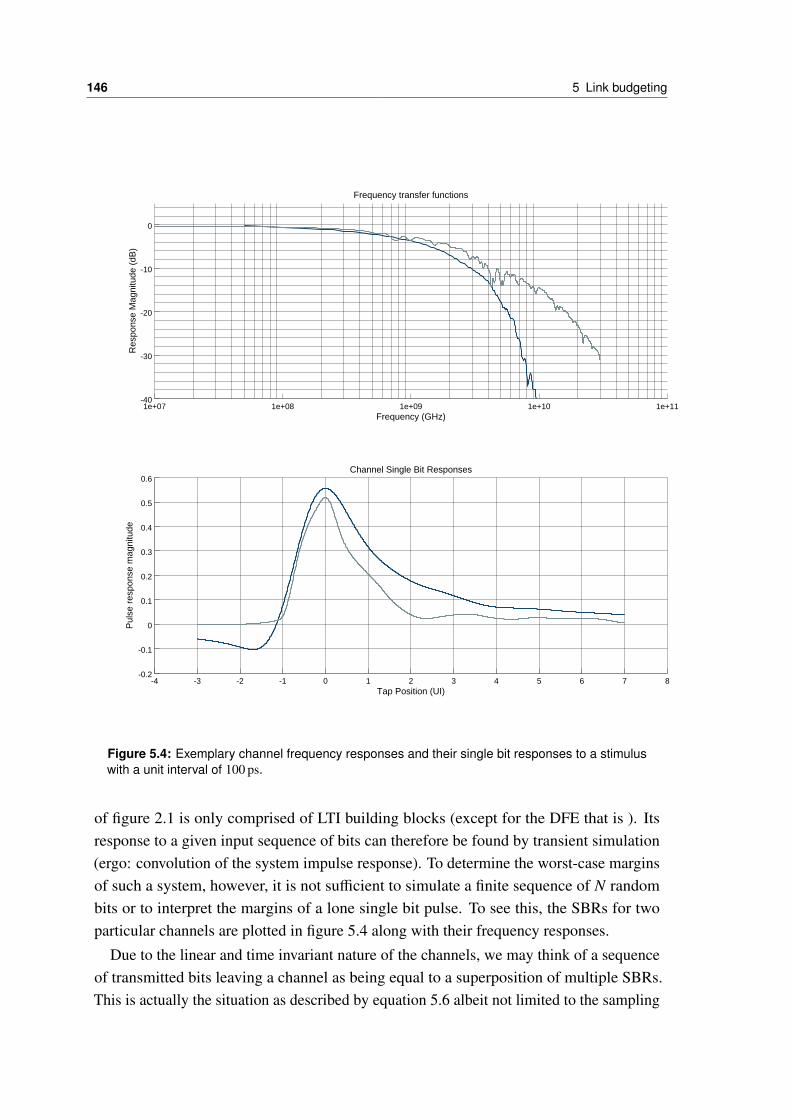
146 5 Link budgeting
1e+07 1e+08 1e+09 1e+10 1e+11-40
-30
-20
-10
0
Frequency (GHz)
Res
pons
e M
agni
tude
(dB
)
-4 -3 -2 -1 0 1 2 3 4 5 6 7 8-0.2
-0.1
0
0.1
0.2
0.3
0.4
0.5
0.6
Tap Position (UI)
Pul
se r
espo
nse
mag
nitu
de
Frequency transfer functions
Channel Single Bit Responses
Figure 5.4: Exemplary channel frequency responses and their single bit responses to a stimuluswith a unit interval of 100 ps.
of figure 2.1 is only comprised of LTI building blocks (except for the DFE that is ). Itsresponse to a given input sequence of bits can therefore be found by transient simulation(ergo: convolution of the system impulse response). To determine the worst-case marginsof such a system, however, it is not sufficient to simulate a finite sequence of N randombits or to interpret the margins of a lone single bit pulse. To see this, the SBRs for twoparticular channels are plotted in figure 5.4 along with their frequency responses.
Due to the linear and time invariant nature of the channels, we may think of a sequenceof transmitted bits leaving a channel as being equal to a superposition of multiple SBRs.This is actually the situation as described by equation 5.6 albeit not limited to the sampling
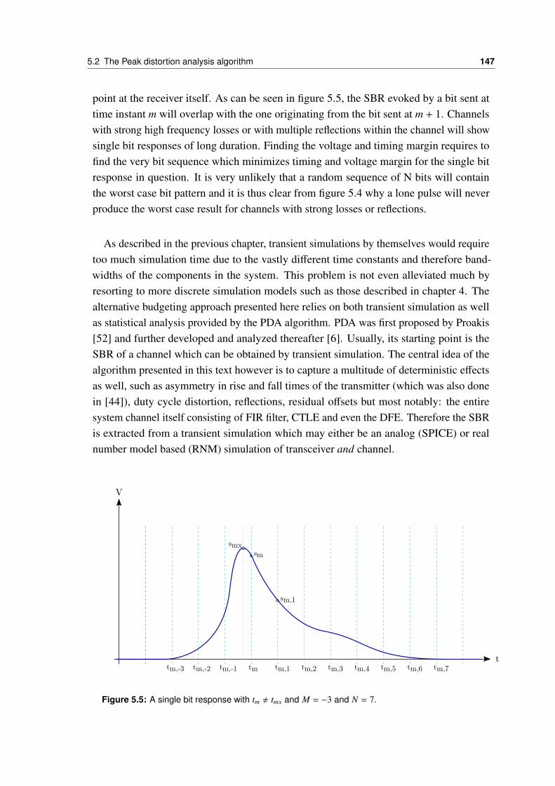
5.2 The Peak distortion analysis algorithm 147
point at the receiver itself. As can be seen in figure 5.5, the SBR evoked by a bit sent attime instant m will overlap with the one originating from the bit sent at m + 1. Channelswith strong high frequency losses or with multiple reflections within the channel will showsingle bit responses of long duration. Finding the voltage and timing margin requires tofind the very bit sequence which minimizes timing and voltage margin for the single bitresponse in question. It is very unlikely that a random sequence of N bits will containthe worst case bit pattern and it is thus clear from figure 5.4 why a lone pulse will neverproduce the worst case result for channels with strong losses or reflections.
As described in the previous chapter, transient simulations by themselves would requiretoo much simulation time due to the vastly different time constants and therefore band-widths of the components in the system. This problem is not even alleviated much byresorting to more discrete simulation models such as those described in chapter 4. Thealternative budgeting approach presented here relies on both transient simulation as wellas statistical analysis provided by the PDA algorithm. PDA was first proposed by Proakis[52] and further developed and analyzed thereafter [6]. Usually, its starting point is theSBR of a channel which can be obtained by transient simulation. The central idea of thealgorithm presented in this text however is to capture a multitude of deterministic effectsas well, such as asymmetry in rise and fall times of the transmitter (which was also donein [44]), duty cycle distortion, reflections, residual offsets but most notably: the entiresystem channel itself consisting of FIR filter, CTLE and even the DFE. Therefore the SBRis extracted from a transient simulation which may either be an analog (SPICE) or realnumber model based (RNM) simulation of transceiver and channel.
V
ttm tm,1 tm,2tm,-1tm,-2tm,-3 tm,3 tm,4 tm,5 tm,6 tm,7
sm
sm,1
smx
Figure 5.5: A single bit response with tm , tmx and M = −3 and N = 7.
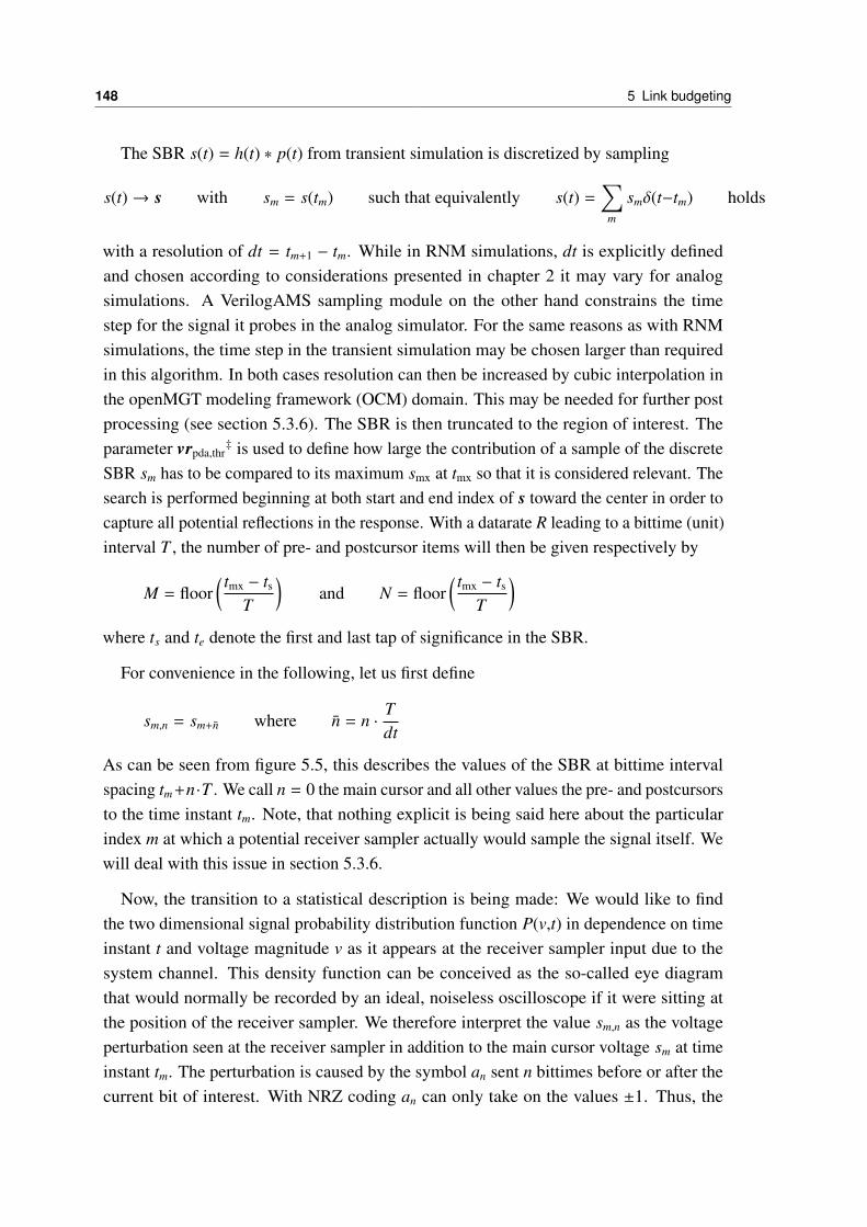
148 5 Link budgeting
The SBR s(t) = h(t) ∗ p(t) from transient simulation is discretized by sampling
s(t)→ s with sm = s(tm) such that equivalently s(t) =∑
m
smδ(t−tm) holds
with a resolution of dt = tm+1 − tm. While in RNM simulations, dt is explicitly definedand chosen according to considerations presented in chapter 2 it may vary for analogsimulations. A VerilogAMS sampling module on the other hand constrains the timestep for the signal it probes in the analog simulator. For the same reasons as with RNMsimulations, the time step in the transient simulation may be chosen larger than requiredin this algorithm. In both cases resolution can then be increased by cubic interpolation inthe openMGT modeling framework (OCM) domain. This may be needed for further postprocessing (see section 5.3.6). The SBR is then truncated to the region of interest. Theparameter vrpda,thr
‡ is used to define how large the contribution of a sample of the discreteSBR sm has to be compared to its maximum smx at tmx so that it is considered relevant. Thesearch is performed beginning at both start and end index of s toward the center in order tocapture all potential reflections in the response. With a datarate R leading to a bittime (unit)interval T , the number of pre- and postcursor items will then be given respectively by
M = floor( tmx − ts
T
)and N = floor
( tmx − ts
T
)where ts and te denote the first and last tap of significance in the SBR.
For convenience in the following, let us first define
sm,n = sm+n where n = n ·Tdt
As can be seen from figure 5.5, this describes the values of the SBR at bittime intervalspacing tm+n·T . We call n = 0 the main cursor and all other values the pre- and postcursorsto the time instant tm. Note, that nothing explicit is being said here about the particularindex m at which a potential receiver sampler actually would sample the signal itself. Wewill deal with this issue in section 5.3.6.
Now, the transition to a statistical description is being made: We would like to findthe two dimensional signal probability distribution function P(v,t) in dependence on timeinstant t and voltage magnitude v as it appears at the receiver sampler input due to thesystem channel. This density function can be conceived as the so-called eye diagramthat would normally be recorded by an ideal, noiseless oscilloscope if it were sitting atthe position of the receiver sampler. We therefore interpret the value sm,n as the voltageperturbation seen at the receiver sampler in addition to the main cursor voltage sm at timeinstant tm. The perturbation is caused by the symbol an sent n bittimes before or after thecurrent bit of interest. With NRZ coding an can only take on the values ±1. Thus, the
5.2 The Peak distortion analysis algorithm 149
voltage perturbations sm,n
∣∣∣n,0
will either increase or decrease sm depending on the actual bitpattern sent prior to the current bit (postcursors) or thereafter (precursors). More formally,we write
sm,nstat−−→ pm,n(v) =
α, v = sm,n and an = +1
1 − α, v = −sm,n and an = −1
0, else
which associates sm,n with the probability density function pm,n(v). Since the SBR iscontinuous in v, so is pm,n(v). It needs to be discretized for numerical processing. Therefore,a parameter vrpdavres
‡ is introduced which defines the binning interval for the voltages dv.The parameter α is directly related to the transmission alphabet coding. For a PRBS the
probability of transmitting and receiving a logic zero or one is equal. Therefore α = 0.5.In order to get the total PDF Pm at a given sampling instant tm, all possible combinationsof bits at the various cursor instants have to be combined. With the convolution of twoPDFs as given in 2.1 we define a cumulative convolution operator for all PDFs pmn at atime instant tm:
Pm =
N∑n=−M
∗ pm,n ≡
N+M−1∑n=0
∗ pm,n
∗ pm,M+N (5.10)
This recursive definition lends itself very well for a parallel implementation as the linearconvolution operation is associative and can thus be executed in any order and with multiplesubdivisions of the available pm,n. The result of this operation will be the probability densityfunction Pm of a signal passing through a particular voltage interval v + dv at time instanttm.
Figure 5.6 shows two different Pm for the light grey SBR shown in figure 5.4. m ischosen such that in one case, it is in between the SBRs maximum and the first precursorto the maximum. In the second case, m aligns with the maximum. At the maximum, thetwo distribution regions around v = ±smx do not overlap. In the absence of further noisesources, the statistical eye is considered "open". A potential sampler of sufficient resolutionand sensitivity might readily convert the incoming analog signal into a valid stream ofdigital bits. In the first case, however, the chosen sampling point would be in very closeproximity to the signal transition region. The two partial distributions overlap and no "eyeopening" is observed at this instant in time.
If the various Pm are concatenated in order of their associated time instant tm, a completestatistical eye can be produced (see figure 5.7). Thus
Peye(v,t) =∑
m
Pm(v)δ(t − tm)
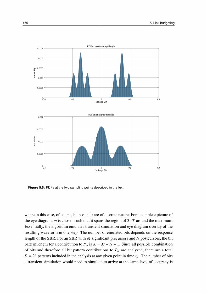
150 5 Link budgeting
-0.4 -0.2 0 0.2 0.40
0.0005
0.001
0.0015
0.002
0.0025
Voltage Bin
Pro
babi
lity
-0.4 -0.2 0 0.2 0.40
0.0005
0.001
0.0015
0.002
Voltage Bin
Pro
babi
lity
PDF at maximum eye height
PDF at left signal transition
Figure 5.6: PDFs at the two sampling points described in the text
where in this case, of course, both v and t are of discrete nature. For a complete picture ofthe eye diagram, m is chosen such that it spans the region of 3 · T around the maximum.Essentially, the algorithm emulates transient simulation and eye diagram overlay of theresulting waveform in one step. The number of emulated bits depends on the responselength of the SBR. For an SBR with M significant precursors and N postcursors, the bitpattern length for a contribution to Pm is K = M + N + 1. Since all possible combinationof bits and therefore all bit pattern contributions to Pm are analyzed, there are a totalS = 2K patterns included in the analysis at any given point in time tm. The number of bitsa transient simulation would need to simulate to arrive at the same level of accuracy is

5.2 The Peak distortion analysis algorithm 151
therefore given by
R = K · S = (M + N + 1) · 2M+N+1
The three parameters of time resolution dt, SBR significance threshold vrpda,thr andvoltage binning resolution vrpdavres determine both the precision of the result as wellas the total runtime of the algorithm. They must be chosen carefully so that runtimeis not increased excessively while only a marginal benefit in accuracy is gained. Thealgorithm was implemented using the OCM framework in conjunction with the Octavesoftware package (see chapter 4 for details on the interaction between simulations and postprocessing within the OCM framework).
0 20 40 60 80 100 120 140
-1
-0.5
0
0.5
1
Sampling instant in ps
Mag
nitu
de V
_1 @
240
.00
mV
5.96e-09
2.40e-04
4.81e-04
7.21e-04
9.61e-04
1.20e-03
1.44e-03
1.68e-03
1.92e-03
2.16e-03
2.40e-03
Figure 5.7: Statistical eye diagram resulting from peak distortion algorithm presented here. Thisfigure
The example presented in figure 5.7 shows the deterministic eye of the SBR correctedby CTLE equalization for the light gray channel. Note that the columns are normalizedto unity so that the probabilities as indicated by the colorbar to the right of the picturealways refer to a time instant. The rows will therefore not be normalized and will requirerenormalization when used as deterministic PDFs. The analysis was carried out with a timeresolution of 1 ps and a voltage resolution of about 600 uV. This lead to five pre- and 21post cursors which therefore accounted for approximately R = 3.6 · 109 statistically treatedbits. Since the unit interval T is 100 ps in this case, the total transient simulation time toarrive at the same result would have been 360 ms accordingly. The algorithm requires atotal computation time of merely 3.5 s in this case for a single SBR to PDA conversion
152 5 Link budgeting
on a 12 core Intel Xeon E5-2630 system running at 2.3 GHz and 96 GByte of RAM (thememory footprint is marginal with a few tens of megabytes).
A disadvantage of the procedure described here is that the actual alphabet coding is notconsidered. It may actually improve the eye if worst case patterns are not contained in it.Links are often tested with PRBS patterns though and if they are held to be the measureof a system passing or failing a specifc BER target, searching for worst case patterns isthe default approach. If the alphabet coding was 8B/10B for instance, the limited set ofallowed sequences will lead to a modified value for α. There is however a way in whicha future algorithm could be improved in this aspect: while still using equal probabilitesfor ones and zeros, the convolution process could be extended to filter out the disallowedsequences by tracking how a partial PDF p(v,t) is generated. If a specific sequence is notcontained in the given alphabet, it could be omitted from further processing. Since there isa lot of lookup effort involved, this may, however, proof computationally intense.
The computationally efficient PDA algorithm presented here forms the foundation ofthe serializer system budgeting and analysis algorithm presented in the following.
5.3 The OCM link budgeting algorithm
This section introduces the budgeting algorithm as it is employed in the openMGT/OCMframework. It combines the benefits of peak distortion algorithm - statistical treatmentand inherent parallelization - with the computational efficiency of treating random phasenoise sources in frequency domain to first order (compare equation 5.1). Its core ideadirectly stems from the concept pursued with the entire openMGT framework: Separationof all deterministic system properties from all random perturbations and treatment of asmany deterministic effects as possible within the transient pre-simulation while delegatingmore complex processes with larger time constants to the OCM/OCD post processingdomain. While the statistical PDA algorithm characterizes deterministic aspects of a giventransmission channel, there are the above-mentioned random contributions such as voltagenoise and timing jitter which originate from random physical processes such as 1/f andthermal noise of the electronic system. System performance constraints originating fromrandom contributions can quite generally be observed by a transient simulation. However,the likeliness of a specific event to occur in simulation is directly related to the probabilityfunction of the underlying process. In a multigigabit link analysis with target bit errorrates of below 1e-12 and simulator time steps in the picosecond range, it is quite evidentthat even the most potent computing platforms will not be able to solve the problem withtransient approaches within a sensible amount of time. Therefore the process of analyzingthe link system is segregated into two distinct portions: Deterministic effects can andmay be observed and checked by simulation approaches. The task of taking random
5.3 The OCM link budgeting algorithm 153
effects into account will entirely be placed inside the numeric modeling domain. This istrue for both random voltage and timing uncertainties. Since the translatation betweenvoltage and timing noise is always possible within the limits described earlier, the formused for budgeting depends on the availability of data from other simulations or on howspecification metrics are defined (which usually depends on the available testequipmentrequired for these meausrements).
Equalization settings provide a very good insight into how well metric constraints arechosen for a particular serializer implementation. Consider a worst case channel as definedby most modern protocol specifications: If it is used for budgeting and the equalizationsettings required are fairly moderate compared to the allocated equalization capabilites,the odds are very high that some part of the system was overconstrained. Often times, thismay be the linear preamplifier in the receiver which incurs a significant power penaltyfor the whole transceiver. This an important reason why equalization training is part ofthe transient pre-simulation for the budgeting procedure. The other is of course the mostdecisive question whether or not the given system can ensure a specific target BER on thetransmission channel in question.
With the physical transmission channel given, the PDA produces a probability densityfunction of a specific voltage to be encountered at the input of a sampler at a particual pointin time (the sampling instant). This two- dimensional PDF of the entire system channellends itself well to be further processed by combining it with probability distributionsof voltage and timing noise sources. The dominant noise source in broadband circuitsis thermal noise (Johnson-Nyquist noise) of the constituent components. Techniques toevaluate the voltage noise added by a given electronic topology to its output signal withrespect to its input are readily available and either analytical or simulation based. From thederived voltage noise power spectral density S VV( f ) the total RMS voltage noise appearingat the output of the circuit can then be computed to
σn =
∞∫0
S vv( f )d f
Due to strict separation of deterministic and random contributions (see figures 5.8 and 5.9),at least the deterministic, two dimesional eye PDF and the random PDFs can be assumedto have originated from entirely uncorrelated sources. This is not be the case for the PDFsof voltage and phase noise since all the components in either PDF that originate from thesame buffer or the same power distribution would indeed be a source of correlation. In thissense, the final outcome of the budgeting procedure is actually conservative.
The deterministic effects which are covered by the openMGT real number models forbudgeting are
• TX duty cycle distortion (DCD) due to static mismatches in the TX clock distri-

154 5 Link budgeting
bution and potential PMOS/NMOS mismatch in the output driver which leads toasymmetries in rising and falling transitions r(t) and f (t)
• The channel response H( jω) as given by either an impulse response or S-Parameterfile
• Transmitter and receiver termination mismatch Γs and Γl, which are mainly due tolarge polyresistor variations in advanced technology nodes and can be compensatedby digitally adjustable resistors with a finite resolution and thus a finite error
• Static mismatches in the receiver analog frontend which even in the presence ofcalibration logic lead to a residual offset error ∆resoff
• Sampler nonidealities as described in section 4.5 which lead to ISF Γ(t), finite dcsensitivity χdc and intrinsic offset ∆off
• Power distribution noise backaction due to the spectrally resolved current consump-tion of the system in cases where ZPDN is known.
PLL & Clock Distribution
+
Clock Data Recovery
PLL & Clock Distribution
Channel RX Analog Frontend
Sampler
DAC & Drivern-Tap Coding
DFE
φref,rx φ
φrxφ
φref,tx
EQan
bn
h(t) H(jω)
ynyn rn
Tap Count nWeights w
r(t), f(t)DCDVpp
hn*
p(t)=
s(t) sn
Hafe(jω)
Γ(t)χdcΔoff
Δresoff
Γs Γl
Figure 5.8: Deterministic effects and their respective subcomponent as used duringOCM link budgeting
A transient pre-simulation will consist of
• Initializing offset correction vectors where applicable such that the residual offseterror will be minimized. This is a shortcut to the calibration routines which arenormally used to find a particular correction vector for a given stage. These loopsare verified separately so it can be assumed here that the optimal code is actuallyretrieved during serializer startup.
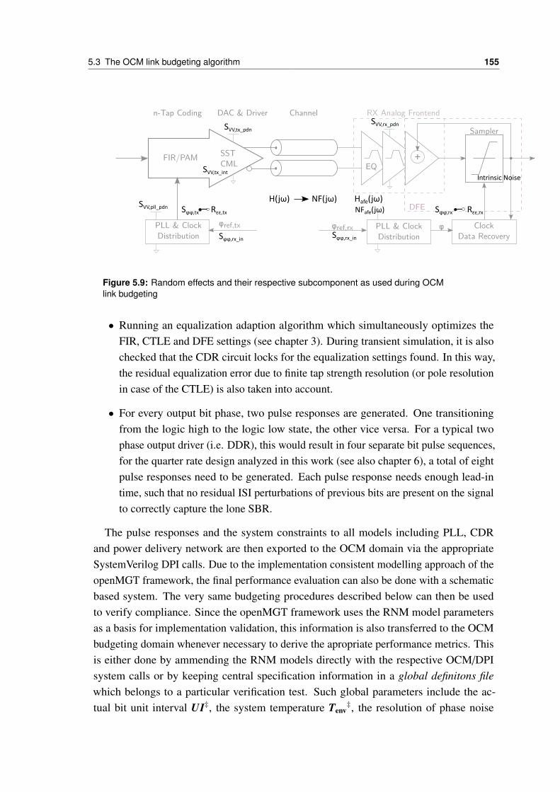
5.3 The OCM link budgeting algorithm 155
PLL & Clock Distribution
+
Clock Data Recovery
PLL & Clock Distribution
Channel RX Analog Frontend
Sampler
DAC & Drivern-Tap Coding
SSTCML
DFE
FIR/PAM
φref,rx φφref,tx
EQ
H(jω) Hafe(jω)
Intrinsic Noise
NFafe(jω)Rεε,tx Sϕϕ,tx Rεε,rx Sϕϕ,rx
Sϕϕ,rx_in
NF(jω)
Sϕϕ,rx_in
SVV,tx_pdn
SVV,tx_int
SVV,pll_pdn
SVV,rx_pdn
Figure 5.9: Random effects and their respective subcomponent as used during OCMlink budgeting
• Running an equalization adaption algorithm which simultaneously optimizes theFIR, CTLE and DFE settings (see chapter 3). During transient simulation, it is alsochecked that the CDR circuit locks for the equalization settings found. In this way,the residual equalization error due to finite tap strength resolution (or pole resolutionin case of the CTLE) is also taken into account.
• For every output bit phase, two pulse responses are generated. One transitioningfrom the logic high to the logic low state, the other vice versa. For a typical twophase output driver (i.e. DDR), this would result in four separate bit pulse sequences,for the quarter rate design analyzed in this work (see also chapter 6), a total of eightpulse responses need to be generated. Each pulse response needs enough lead-intime, such that no residual ISI perturbations of previous bits are present on the signalto correctly capture the lone SBR.
The pulse responses and the system constraints to all models including PLL, CDRand power delivery network are then exported to the OCM domain via the appropriateSystemVerilog DPI calls. Due to the implementation consistent modelling approach of theopenMGT framework, the final performance evaluation can also be done with a schematicbased system. The very same budgeting procedures described below can then be usedto verify compliance. Since the openMGT framework uses the RNM model parametersas a basis for implementation validation, this information is also transferred to the OCMbudgeting domain whenever necessary to derive the apropriate performance metrics. Thisis either done by ammending the RNM models directly with the respective OCM/DPIsystem calls or by keeping central specification information in a global definitons filewhich belongs to a particular verification test. Such global parameters include the ac-tual bit unit interval UI‡, the system temperature Tenv
‡, the resolution of phase noise

156 5 Link budgeting
functions d fφ‡, the (random) digital test sequence used during analysis as well as thesupply voltage level and (in verification runs) the technology corner used. As describedin sections 4.4 and 4.5 the actual component modelling for channel and sampler is imple-mented in the OCM domain itself. In this case, the information required for postprocessingis already in place and consistent with the data used throughout the transient pre simulation.
Post processing is separated into seven distinct steps which may themselves be furtherbroken down into substeps.
5.3.1 Power distribution
The budgeting procedure checks for the presence of a PDN impedance profile for PLL,RX and TX. This can either be an impedance mask or a more realistic impedance curve asgenerated by EM extraction of board and package together with the known characteristicsof VRM and capacitances. In order to use the impedance profiles, a file describingthe subcomponents spectral current consumption must also be supplied. This currentprofile can potentially be obtained together with the transient budgeting simulation itself,provided that all subcomponents of the system feature activity dependent power modelsor a full schematic based transient simulation has been carried out. In the absence of thisinformation (which is typical for a predesign phase), the procedure reverts to the simplebox or lowpass noise model specified by the global defintions file. How the informationis being processed from this point onward depends on the actual subcomponent and isdescribed in the respective sections below.
5.3.2 PLL phase noise spectral density for transmitter and receiver
Referring to section 2.2.4, it is possible to use and constrain parameters for the subcompo-nents of the PLL as a basis for further link budgeting. The budgeting procedure compilesthe information from the global definition file and uses the equations described to producethe phase noise spectral density S φφ. They are used both for the transmitter and the receiverunless the phase noise properties of their respective clock distribution is known as well. Incases where system components are already designed, the more accurate, simulation basedphase noise PSDs may and should be used instead of the model. The model, howevercan always be used as a compliance check for the actual implementation. Once the PLLphase noise spectral density S φφ,PLL is computed, a global parameter magφ,t rsh
‡ is used todetermine the phase noise bandwidth ωφ,BW
‡, i.e. the frequency range to be consideredduring phase noise analysis in all subsequent steps. Since there is also a strict separationbetween voltage and phase noise sources in the budgeting flow and we expect the majorrandom contributions to phase noise in the system to mainly arise from the PLL itself, thislimitation keeps the phase noise vector at manageable sizes.
5.3 The OCM link budgeting algorithm 157
5.3.3 Peak distortion analysis
The PDA algorithm is the central element of the budgeting procedure. As mentioned insection 5.2, the statistical algorithm is used to decrease the transient simulation time andto acquire an accurate estimate of the two-dimensional eye PDF at the sampler input andis as such a complete representation of yisi,m in equation 5.6 for all potential samplingpoints m. Here, we extend the idea of the intersymbol interference term. First, it alsocovers the residual signal deterioration which is due to imperfect equalization. Also, itcovers the effects of residual offsets in all equalization stages. And finally, the deterministiceffect of duty cycle distortion is also taken into account as part of the transient simulation.The resulting estimation thus not only absorbs the effects of the FIR weighting matrixW, but also captures the signal improvement efforts of CTLE and DFE without havingto describe their effects in the time domain mathematically - literature on budgeting andsystem performance estimation usually does not cover these aspects at all. In addition,since the serializer system is simulated in conjunction with its calibration and equalizationloops, the quality of their respective result is considered implicitly. This helps to choosethe right dimensions for calibration vectors and filter constants for the respective controlloops. Due to this great degree of coverage, a more appropriate symbol for the resultingquantities is Peye, det,v,tm .
One of the central TX and RX design parameters is the number of clock phases usedfor (de-) serialization. If the final retiming stage of the transmitter is double data rate anddifferential, it requires two clock phases. If a receiver is said to be a quarter rate design, ituses four distinct clock phases with its four data samplers. In order to capture the effects ofduty cycle distortion, the resulting PDA needs to be calculated from equally many distinctsingle bit responses as there are clock phases in the transmitter. The distinct SBRs needto originate from the respective clock phases and will lead to differing, determinstic eyeheights and widths. In order to capture asymmetries in transmitter rise and fall times ornonlinearities in the preamplification stages of the receiver, for every TX output phaseboth logic transitions will be simulated. For a quarter rate design for instance, this resultsin a total of eight single bit responses to be analyzed seperately. The resulting statisticaleyes will be weighted equally and summed. Strictly speaking, the transmission alphabetwould need to be factored in at this point as it may exhibit a statistical imbalance betweenthe logic levels. Since the PDA itself, however is also calculated under the assumption ofequal probabilities for all logic levels, this notion is perpetuated here. The requirement ofcalculating multiple statistical eye diagrams is also a major reason for the parallelizationefforts during the development of the OCM PDA algorithm.
Figure 5.10 depicts the result of a statistical system channel analysis with the serializersystem as presented in the next chapter. The system does not perform proper equlization.As a result, the statistical eye is almost closed, even in the absence of superimposed voltage
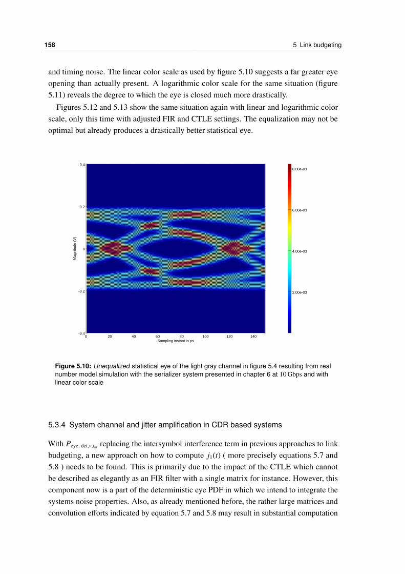
158 5 Link budgeting
and timing noise. The linear color scale as used by figure 5.10 suggests a far greater eyeopening than actually present. A logarithmic color scale for the same situation (figure5.11) reveals the degree to which the eye is closed much more drastically.
Figures 5.12 and 5.13 show the same situation again with linear and logarithmic colorscale, only this time with adjusted FIR and CTLE settings. The equalization may not beoptimal but already produces a drastically better statistical eye.
0 20 40 60 80 100 120 140-0.4
-0.2
0
0.2
0.4
Sampling instant in ps
Mag
nitu
de (
V)
2.00e-03
4.00e-03
6.00e-03
8.00e-03
Figure 5.10: Unequalized statistical eye of the light gray channel in figure 5.4 resulting from realnumber model simulation with the serializer system presented in chapter 6 at 10 Gbps and withlinear color scale
5.3.4 System channel and jitter amplification in CDR based systems
With Peye, det,v,tm replacing the intersymbol interference term in previous approaches to linkbudgeting, a new approach on how to compute j1(t) ( more precisely equations 5.7 and5.8 ) needs to be found. This is primarily due to the impact of the CTLE which cannotbe described as elegantly as an FIR filter with a single matrix for instance. However, thiscomponent now is a part of the deterministic eye PDF in which we intend to integrate thesystems noise properties. Also, as already mentioned before, the rather large matrices andconvolution efforts indicated by equation 5.7 and 5.8 may result in substantial computation
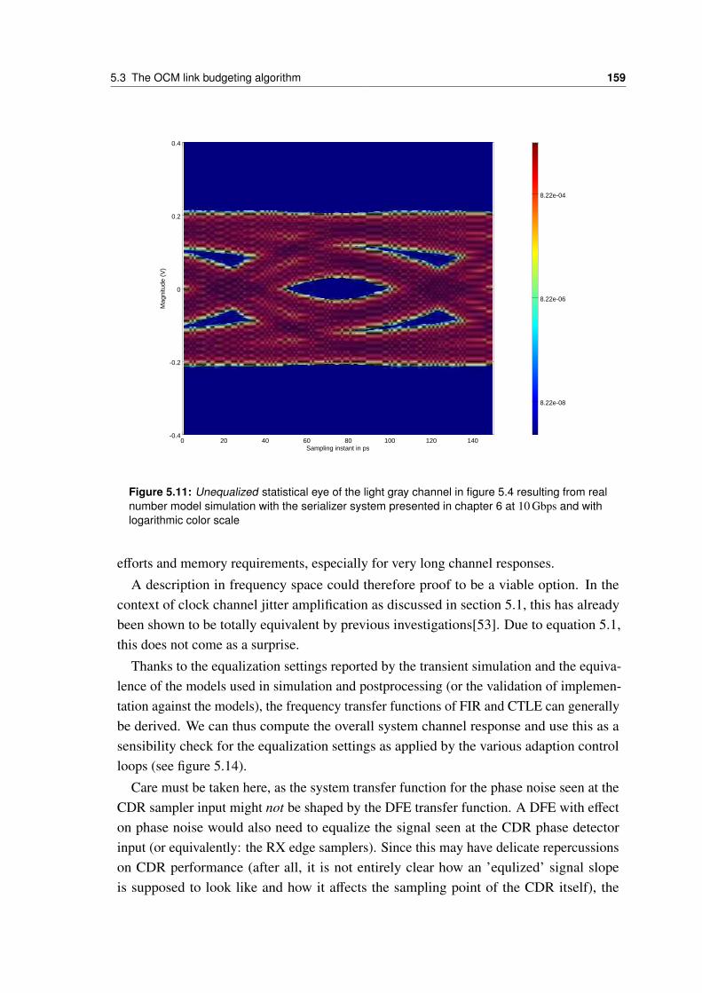
5.3 The OCM link budgeting algorithm 159
0 20 40 60 80 100 120 140-0.4
-0.2
0
0.2
0.4
Sampling instant in ps
Mag
nitu
de (
V)
8.22e-04
8.22e-06
8.22e-08
Figure 5.11: Unequalized statistical eye of the light gray channel in figure 5.4 resulting from realnumber model simulation with the serializer system presented in chapter 6 at 10 Gbps and withlogarithmic color scale
efforts and memory requirements, especially for very long channel responses.
A description in frequency space could therefore proof to be a viable option. In thecontext of clock channel jitter amplification as discussed in section 5.1, this has alreadybeen shown to be totally equivalent by previous investigations[53]. Due to equation 5.1,this does not come as a surprise.
Thanks to the equalization settings reported by the transient simulation and the equiva-lence of the models used in simulation and postprocessing (or the validation of implemen-tation against the models), the frequency transfer functions of FIR and CTLE can generallybe derived. We can thus compute the overall system channel response and use this as asensibility check for the equalization settings as applied by the various adaption controlloops (see figure 5.14).
Care must be taken here, as the system transfer function for the phase noise seen at theCDR sampler input might not be shaped by the DFE transfer function. A DFE with effecton phase noise would also need to equalize the signal seen at the CDR phase detectorinput (or equivalently: the RX edge samplers). Since this may have delicate repercussionson CDR performance (after all, it is not entirely clear how an ’equlized’ signal slopeis supposed to look like and how it affects the sampling point of the CDR itself), the

160 5 Link budgeting
0 20 40 60 80 100 120 140-0.4
-0.2
0
0.2
0.4
Sampling instant in ps
Mag
nitu
de (
V)
1.00e-03
2.00e-03
3.00e-03
4.00e-03
5.00e-03
Figure 5.12: Equalized statistical eye of the light gray channel in figure 5.4 resulting from realnumber model simulation with the serializer system presented in chapter 6 at 10 Gbps with linearcolor scale
phase detector is usally supplied with the signal as output by the receivers analog frontend.This aspect of system design will be an interesting future topic for which the openMGTframework may be very useful and is not covered further in this text since the serializerdesign to be analyzed in chapter 6, does indeed not correct the edge path (see figure 6.3).
With a frequency description of the system channel available, the key ideas of thisapproach can now be developed:
first, instead of using the ACF of the PLL jitter input to the TX, we use its Fourier trans-form - the power spectral density. Rεtxεtx(t) S φφ,tx(ω) Although potentially recomputableto a frequency power spectral density (referring it to the oscillation carrier), the ansatzin [53] suggests a more elegant alternative which directly uses the one sided phase noisespectral density. This view is particularly helpful here as the second idea directly benefitsfrom this thought:
We view the clock recovery circuit as a special kind of phase locked loop. Its majorproperty is its capability of working with multiple, divided versions of the same referenceclock embedded in the data stream at once in order to recover the phase and frequencyoffset between the embedded clock and the local oscillator. This ensemble of frequenciesresults from the different patterns and run-lengths of logic ones and zeros in the incoming
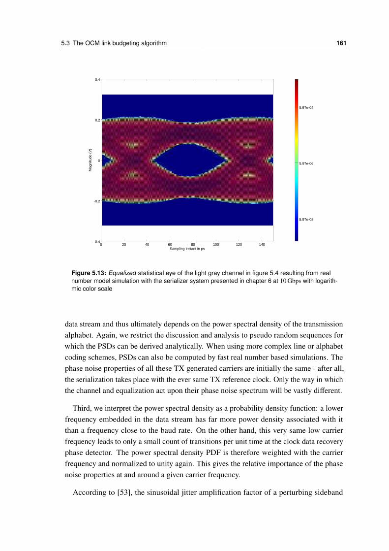
5.3 The OCM link budgeting algorithm 161
0 20 40 60 80 100 120 140-0.4
-0.2
0
0.2
0.4
Sampling instant in ps
Mag
nitu
de (
V)
5.97e-04
5.97e-06
5.97e-08
Figure 5.13: Equalized statistical eye of the light gray channel in figure 5.4 resulting from realnumber model simulation with the serializer system presented in chapter 6 at 10 Gbps with logarith-mic color scale
data stream and thus ultimately depends on the power spectral density of the transmissionalphabet. Again, we restrict the discussion and analysis to pseudo random sequences forwhich the PSDs can be derived analytically. When using more complex line or alphabetcoding schemes, PSDs can also be computed by fast real number based simulations. Thephase noise properties of all these TX generated carriers are initially the same - after all,the serialization takes place with the ever same TX reference clock. Only the way in whichthe channel and equalization act upon their phase noise spectrum will be vastly different.
Third, we interpret the power spectral density as a probability density function: a lowerfrequency embedded in the data stream has far more power density associated with itthan a frequency close to the baud rate. On the other hand, this very same low carrierfrequency leads to only a small count of transitions per unit time at the clock data recoveryphase detector. The power spectral density PDF is therefore weighted with the carrierfrequency and normalized to unity again. This gives the relative importance of the phasenoise properties at and around a given carrier frequency.
According to [53], the sinusoidal jitter amplification factor of a perturbing sideband

162 5 Link budgeting
1e+07 1e+08 1e+09 1e+10 1e+11-40
-30
-20
-10
0
10
Frequency (GHz)
Res
pons
e M
agni
tude
(dB
)
channel tfFIR and CTLE correctionsystem tf
System transfer function
Figure 5.14: Equalized system channel response of the light gray channel in figure 5.4 resultingfrom real number model simulation and equalization adaption with the serializer system presentedin chapter 6 and the statistical eye as presented in figure 5.13
0 1e+09 2e+09 3e+09 4e+090
1
2
3
4
5
6
Offset from clock frequency
SJ
ampl
ifica
tion
fact
or
@ 125 MHz@ 5 GHz@ 10 GHz
Figure 5.15: Sinusoidal jitter amplification factor for the dark grey channel in figure 5.4 and forvarious clock center frequencies
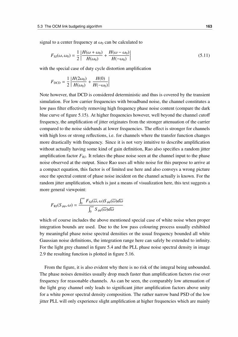
5.3 The OCM link budgeting algorithm 163
signal to a center frequency at ω0 can be calculated to
FSJ(ω,ω0) =12
∣∣∣∣∣H(ω + ω0)H(ω0)
+H(ω − ω0)
H(−ω0)
∣∣∣∣∣ (5.11)
with the special case of duty cycle distortion amplification
FDCD =12
∣∣∣∣∣H(2ω0)H(ω0)
+H(0)
H(−ω0)
∣∣∣∣∣Note however, that DCD is considered deterministic and thus is covered by the transientsimulation. For low carrier frequencies with broadband noise, the channel constitutes alow pass filter effectively removing high frequency phase noise content (compare the darkblue curve of figure 5.15). At higher frequencies however, well beyond the channel cutofffrequency, the amplification of jitter originates from the stronger attenuation of the carriercompared to the noise sidebands at lower frequencies. The effect is stronger for channelswith high loss or strong reflections, i.e. for channels where the transfer function changesmore drastically with frequency. Since it is not very intuitive to describe amplificationwithout actually having some kind of gain definition, Rao also specifies a random jitteramplification factor FRJ. It relates the phase noise seen at the channel input to the phasenoise observed at the output. Since Rao uses all white noise for this purpose to arrive ata compact equation, this factor is of limited use here and also conveys a wrong pictureonce the spectral content of phase noise incident on the channel actually is known. For therandom jitter amplification, which is just a means of visualization here, this text suggests amore general viewpoint:
FRJ(S φφ, ω) =
∫ ∞0
FSJ(ω,ω)S φφ(ω)dω∫ ∞0
S φφ(ω)dω
which of course includes the above mentioned special case of white noise when properintegration bounds are used. Due to the low pass colouring process usually exhibitedby meaningful phase noise spectral densities or the usual frequency bounded all whiteGaussian noise definitions, the integration range here can safely be extended to infinity.For the light grey channel in figure 5.4 and the PLL phase noise spectral density in image2.9 the resulting function is plotted in figure 5.16.
From the figure, it is also evident why there is no risk of the integral being unbounded.The phase noises densities usually drop much faster than amplification factors rise overfrequency for reasonable channels. As can be seen, the comparably low attenuation ofthe light gray channel only leads to significant jitter amplification factors above unityfor a white power spectral density composition. The rather narrow band PSD of the lowjitter PLL will only experience slight amplification at higher frequencies which are mainly
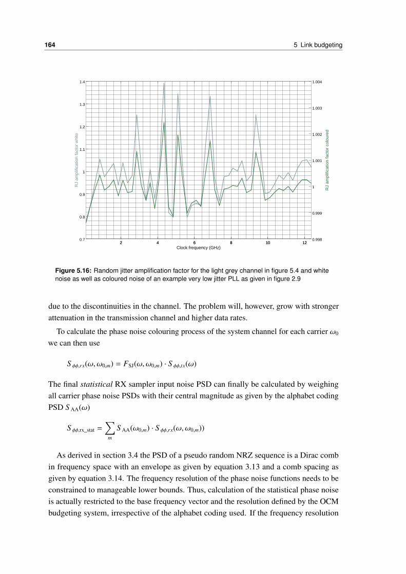
164 5 Link budgeting
2 4 6 8 10 120.7
0.8
0.9
1
1.1
1.2
1.3
1.4
Clock frequency (GHz)
RJ
ampl
ifica
tion
fact
or w
hite
2 4 6 8 10 120.998
0.999
1
1.001
1.002
1.003
1.004
RJ
ampl
ifica
tion
fact
or c
olou
red
Figure 5.16: Random jitter amplification factor for the light grey channel in figure 5.4 and whitenoise as well as coloured noise of an example very low jitter PLL as given in figure 2.9
due to the discontinuities in the channel. The problem will, however, grow with strongerattenuation in the transmission channel and higher data rates.
To calculate the phase noise colouring process of the system channel for each carrier ω0
we can then use
S φφ,rx(ω,ω0,m) = FSJ(ω,ω0,m) · S φφ,tx(ω)
The final statistical RX sampler input noise PSD can finally be calculated by weighingall carrier phase noise PSDs with their central magnitude as given by the alphabet codingPSD S AA(ω)
S φφ,rx_stat =∑
m
S AA(ω0,m) · S φφ,rx(ω,ω0,m))
As derived in section 3.4 the PSD of a pseudo random NRZ sequence is a Dirac combin frequency space with an envelope as given by equation 3.13 and a comb spacing asgiven by equation 3.14. The frequency resolution of the phase noise functions needs to beconstrained to manageable lower bounds. Thus, calculation of the statistical phase noiseis actually restricted to the base frequency vector and the resolution defined by the OCMbudgeting system, irrespective of the alphabet coding used. If the frequency resolution
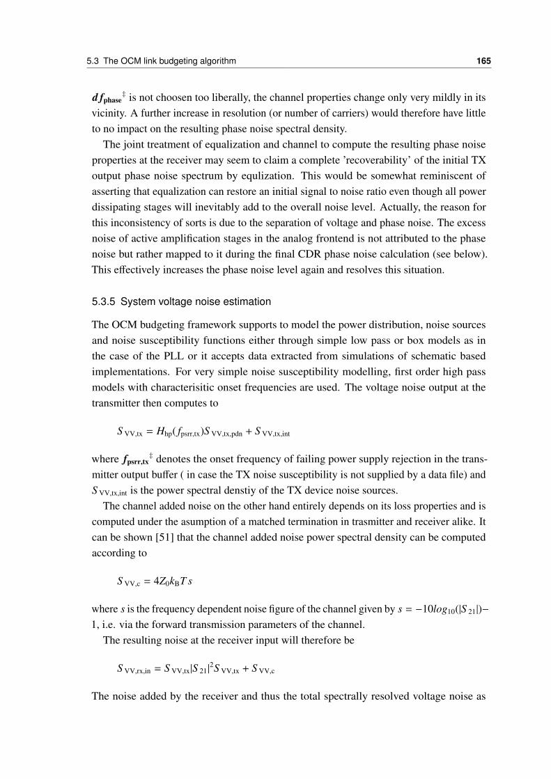
5.3 The OCM link budgeting algorithm 165
d fphase‡ is not choosen too liberally, the channel properties change only very mildly in its
vicinity. A further increase in resolution (or number of carriers) would therefore have littleto no impact on the resulting phase noise spectral density.
The joint treatment of equalization and channel to compute the resulting phase noiseproperties at the receiver may seem to claim a complete ’recoverability’ of the initial TXoutput phase noise spectrum by equlization. This would be somewhat reminiscent ofasserting that equalization can restore an initial signal to noise ratio even though all powerdissipating stages will inevitably add to the overall noise level. Actually, the reason forthis inconsistency of sorts is due to the separation of voltage and phase noise. The excessnoise of active amplification stages in the analog frontend is not attributed to the phasenoise but rather mapped to it during the final CDR phase noise calculation (see below).This effectively increases the phase noise level again and resolves this situation.
5.3.5 System voltage noise estimation
The OCM budgeting framework supports to model the power distribution, noise sourcesand noise susceptibility functions either through simple low pass or box models as inthe case of the PLL or it accepts data extracted from simulations of schematic basedimplementations. For very simple noise susceptibility modelling, first order high passmodels with characterisitic onset frequencies are used. The voltage noise output at thetransmitter then computes to
S VV,tx = Hhp( fpsrr,tx)S VV,tx,pdn + S VV,tx,int
where fpsrr,tx‡ denotes the onset frequency of failing power supply rejection in the trans-
mitter output buffer ( in case the TX noise susceptibility is not supplied by a data file) andS VV,tx,int is the power spectral denstiy of the TX device noise sources.
The channel added noise on the other hand entirely depends on its loss properties and iscomputed under the asumption of a matched termination in trasmitter and receiver alike. Itcan be shown [51] that the channel added noise power spectral density can be computedaccording to
S VV,c = 4Z0kBT s
where s is the frequency dependent noise figure of the channel given by s = −10log10(|S 21|)−1, i.e. via the forward transmission parameters of the channel.
The resulting noise at the receiver input will therefore be
S VV,rx,in = S VV,tx|S 21|2S VV,tx + S VV,c
The noise added by the receiver and thus the total spectrally resolved voltage noise as
166 5 Link budgeting
appearing on the sampler input can then be caculated to
S VV,rx = Hhp( fpsrr,rx)S VV,rx,pdn + S VV,rx,int + |Hrx|2S VV,rx,in
Actually, S VV,rx,int would depend on the chosen equalization setting Hrx. This couldpotentially be considered in the future. For the purpose of budgeting here, it shall representthe worst case added receiver noise.
In addition to the transmitter, channel and receiver induced noise contributions, one ofthe most important aspects is the sampler self induced noise (see section 4.5). The samplernoise simulation results are not spectrally resolved and therefore require the input referredsampler RMS voltage noise to be considered spectrally white finally giving
S VV,sampler,in = S VV,rx + S VV,sampler,self
Figure 5.17 gives an exemplary overview of the various noise sources and shapingprocesses with the final voltage noise PSD at the sampler input on the lower right.
1e+05 1e+06 1e+07 1e+08 1e+09 1e+10-110
-105
-100
-95
-90
-85
Frequency (Hz)
Pow
er S
pect
ral D
ensi
ty d
B
PDNTX thermalRX thermalSampler self noise
1e+05 1e+06 1e+07 1e+08 1e+09 1e+100
0.002
0.004
0.006
0.008
0.01
Frequency (GHz)
Res
pons
e M
agni
tude
(dB
)
TX PSRRRX PSRR
1e+05 1e+06 1e+07 1e+08 1e+09 1e+10-170
-160
-150
-140
-130
-120
-110
-100
Frequency (Hz)
Pow
er S
pect
ral D
ensi
ty d
B
TX OutputChannel contributionRx Input
1e+05 1e+06 1e+07 1e+08 1e+09 1e+10-97
-96.5
-96
-95.5
-95
-94.5
-94
-93.5
Frequency (Hz)
Pow
er S
pect
ral D
ensi
ty d
B
at sampler
Figure 5.17: Random voltage noise sources in transmitter, channel and receiver and as they maybe commonly present in the system and finally appear at the receiver sampler input.
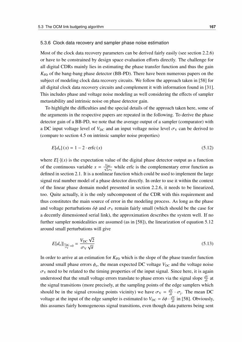
5.3 The OCM link budgeting algorithm 167
5.3.6 Clock data recovery and sampler phase noise estimation
Most of the clock data recovery parameters can be derived fairly easily (see section 2.2.6)or have to be constrained by design space evaluation efforts directly. The challenge forall digital CDRs mainly lies in estimating the phase transfer function and thus the gainKPD of the bang-bang phase detector (BB-PD). There have been numerous papers on thesubject of modeling clock data recovery circuits. We follow the approach taken in [58] forall digital clock data recovery circuits and complement it with information found in [31].This includes phase and voltage noise modeling as well considering the effects of samplermetastability and intrinsic noise on phase detector gain.
To highlight the difficulties and the special details of the approach taken here, some ofthe arguments in the respective papers are repeated in the following. To derive the phasedetector gain of a BB-PD, we note that the average output of a sampler (comparator) witha DC input voltage level of VDC and an input voltage noise level σV can be derived to(compare to section 4.5 on intrinsic sampler noise properties)
E[dn] (x) = 1 − 2 · erfc (x) (5.12)
where E[·](x) is the expectation value of the digital phase detector output as a functionof the continuous variable x = VDC√
2σVwhile erfc is the complementary error function as
defined in section 2.1. It is a nonlinear function which could be used to implement the largesignal real number model of a phase detector directly. In order to use it within the contextof the linear phase domain model presented in section 2.2.6, it needs to be linearized,too. Quite actually, it is the only subcomponent of the CDR with this requirement andthus constitutes the main source of error in the modeling process. As long as the phaseand voltage perturbations δφ and σV remain fairly small (which should be the case fora decently dimensioned serial link), the approximation describes the system well. If nofurther sampler nonidealities are assumed (as in [58]), the linearization of equation 5.12around small perturbations will give
E[dn]| VDCσV≈0 =
VDC√
2σV√π
(5.13)
In order to arrive at an estimation for KPD which is the slope of the phase transfer functionaround small phase errors φe, the mean expected DC voltage VDC and the voltage noiseσV need to be related to the timing properties of the input signal. Since here, it is againunderstood that the small voltage errors translate to phase errors via the signal slope dV
dt atthe signal transitions (more precisely, at the sampling points of the edge samplers whichshould be in the signal crossing points vicinity) we have σV =
dVdt · σj. The mean DC
voltage at the input of the edge sampler is estimated to VDC = δφ ·dVdt in [58]. Obviously,
this assumes fairly homogeneous signal transitions, even though data patterns being sent

168 5 Link budgeting
will produce ISI and consequently different signal slopes. Also, this assumes the samplerto be equally sensitive to changes at the input irrespective of the phase error magnitude(which is equivalent to a static sampler sensitivity function). Finally, it asserts that dcsensitivity does not depend on the previous decision made by the sampler (i.e. there is nometastability). Instead, [58] estimates a well equalized signal at the edge sampler inputto have an amplitude of 2A and a slope dV
dt = A/2 (in units of Vrad) which is equivalent to
2A/T in units of Vs . More simply put, this assumes full height of the eye at the center of
the UI which may not at all be the case. The height of course depends on the success ofthe system equalization efforts which are again an integral part of the OCM budgetingprocedure. In general, the resulting deterministic jitter PDF will be heavily dependent onthe channel and the equalization properties of FIR and CTLE and will not at all adhere to aGaussian distribution. It is customary and also done in [58] to perform a Gaussian fit tothe deterministic PDF in order to derive a reasonable approximation for σj. With theseassumptions, the phase detector gain can be estimated to
KPD =1
σ j√
2π(5.14)
in units of rad−1. If the intrinsic offsets of data and edge samplers are not compensated bycalibration, this will lead to a dead-band in the phase transfer function (compare figure5.18 from [58]). The CDR will then wander around the actual target sampling point sincethere is no meaningful phase detector gain for small phase errors. Since the samplersare offset calibrated within the openMGT OCM budgeting procedure, however, we cansafely assume this error to be very small and consider it absorbed by the usual CDR clockdithering (see below). When looking at the sampling point distribution which can berecorded for smaller periods of time during transient simulations, one can verify that thisassumption actually is justified for a given implementation.
Yet another, numeric way to derive KPD is to initially model the phase detector witha step transfer function and take the ensemble average over jitter present at the input toarrive at the expectation value for the output E[dn] [31]. This can be done by convolvingthe jitter PDF with the ideal step function. Numerically, this is the same as arriving atequation 5.12 directly - a very interesting circumstance, since it opens a path for integratingthe deterministic components of jitter at the sampler input (such as ISI) in the analysispresented here. In addition to phase noise present at the (edge) sampler input, we haveto consider the samplers intrinsic property of metastability. It has been suggested [31] toderive the malicious impact of metastability on KPD by transient (all-digital) simulationswith pseudo random input sequences. On the other hand, metastability is a deterministicproperty of the sampler and is well characterized by the ISF of the sampler (see section4.5. We will therefore suggest an alternate path further below for deriving an approximatevalue of KPD.

5.3 The OCM link budgeting algorithm 169
Figure 5.18: Phase detector transfer charac-teristics under the influence of varying data toedge sampler offset mismatches (from [58]).This problem can be alleviated by proper sam-pler calibration which is an essential part ofthe OCM budgeting procedure.
Finally, there are two sources of intrinsic sampler noise that also need to be taken intoaccount here. The first is the broadband intrisic noise of the sampler itself which is referredback to an equivalent input voltage noise and can in turn be mapped to an input phase noise.This noise source is uncorrelated with any noise appearing on the sampler input whichallows its resulting noise PDF to be directly convoluted with the jitter PDF at the input.The second source is the so-called self noise. The BB-PD produces a binary decision bitfor every clock signal transition and an early/late decision for every signal transition. Thequantization noise is therefore
√2 and is white and broadband in nature. The consequence
of this noise source is a dithering of the CDR position around its ideal position which getsmore severe when CDR bandwidth is not limited [58]. This behavior can be modeled byrefering the self noise of the phase detector back to its input, too. It can be shown that thenoise source has an equivalent RMS magnitude of
√πσj. Assuming again this source of
noise is uncorrelated with the rest, its PDF can again be convoluted with the input phasenoise PDF.
Now that the ideas and problems central to the acquisition of a good estimate of Kpd havebeen presented, the custom OCM budgeting approach can be outlined. The idea is basedon the following observations. For one, the phase detector and CDR system performanceare affected much differently by deterministic, mainly ISI induced jitter and by random,noise induced jitter. The former is spectrally located at very high frequencies (after all, ISIdepends on the specifc bit sequence sent) and can therefore not be rejected/tracked by theCDR. However, its peak to peak value usually is much greater than that of the randomnoise contribution while at the same time it will not adhere to a Gaussian distribution.However, it is the specific nature of this very distribution which determines the actual

170 5 Link budgeting
shape of the phase detector transfer function. On the other hand the random noise sourcesmake a much smaller contribution to overall phase gain degradation but do have a lot ofspectral content within the CDRs tracking range. Parts of it may therefore be rejected bythe CDR. Also, the random noise sources are unbounded. For very low BER operationit is equally important to achieve a good equalization as it is to lower the noise levels atevery possible location. All of these preliminary thoughts lead to the following sequenceof evaluation.
First, the histogram of the deterministic jitter is determined. The construction of thestatistical, deterministic eye of the system channel by performing the PDA analysis takescare of this step - the PDF at the voltage threshold P0(t) = Peye(0, t) can then be usedfor this purpose. The random jitter and voltage noise sources appearing at the inputof the sampler have also been found in the previous step. They are available as phasenoise power and voltage power spectral density. This information will be needed twice.First, to calculate the overall phase noise level at the phase detector and therefore thelinearized CDR loop characteristics. In this first case, the information contained in thespectral densities is simply reduced to the resulting RMS noise level and associated withthe appropriate Gaussian PDF. And second, once the linearized model is obtained, theCDR transfer function can be calculated and used to color the spectral noise densities atthe inputs to finally arrive at a residual phase noise level and calculate its detrimental effecton the deterministic eye width.
Therefore, instead of using the simple deterministic transition PDF at the thresholdas suggested above, the deterministic eye is first convoluted with the voltage noise PDFwhich also has the effect of averaging the potentially sparsely populated matrix elementsaround the transition. A resulting deterministic, ISI induced PDF with random voltagenoise contribution is shown in figure 5.19 as it results from the deterministic eye diagramand the sampler input voltage noise as given in figures 5.13 and 5.17 respectively.
Now, the random contributions to jitter as seen at the CDR input also have to be takeninto account. The previously obtained time interval error PDF is therefore convoluted withthe PDFs of the statistical receiver input phase noise spectral density (potentially degradedby channel jitter amplification) as well as by the receiver reference clock jitter PDF andthe phase interpolator dither PDF whose magnitude is given by the phase interpolatorresolution and the current data rate via
φPI,mag = KDPC · T
in case of a digital dither with a magnitude of a least significant PI bit. The resulting,complete time interval error PDF can be seen in figure 5.20.
It is now asserted here, that the PD characteristic of metastability can be obtained byconvolution of the ideal, step like phase detector characteristic (blue curve in figure 5.21)
5.3 The OCM link budgeting algorithm 171
-20 -10 0 10 200
0.001
0.002
0.003
0.004
0.005
0.006
Time (ps)
Pro
babi
lity
dens
ity in
1 /
( 0.
1 ps
)Time interval error PDF of deterministic signal transition with voltage noise contribution
Figure 5.19: Preliminary probability density function as it may appear at the sampler inputs of aCDR circuit.
with the complete TIE PDF (grey curve) and the impulse sensitivity function of the sampler,resulting in the red curve of figure 5.21. As described in section 4.5 the convolution of theISF with a step function will lead to a value that, if compared to the samplers dc sensitivitythreshold, will determine if a digital zero or one is resolved. The sensitivity parameteraffects the decision depending on the previously resolved bit. If the process of comparison(thus, digital resolution) is omitted, we instead obtain the expectation value E[dn] of theensemble average of all possible data pattern combinations with their signal transitionsall located at the specified phase offset to the sampling clock instant. Just this time, theexpectation value is not resulting from phase noise present at the phase detectors input, butfrom its intrinsic, metastable behavior (which by itself is of course deterministic) and therandom resolved states of the sampler which are due to the randomness of the receiveddata. Strictly speaking, this assumption only holds if logic zeros and ones are equallyprobable within the data stream (an assumption already made in the context of constructingthe PDA statistical eye). We then take the derivative at a phase error of zero. The processof obtaining Kpd involves the consideration of all input noise sources in their unfiltered

172 5 Link budgeting
-3 -2 -1 0 1 2 30
0.01
0.02
0.03
0.04
0.05
0.06
Time (ps)
Pro
babi
lity
dens
ity in
1 /
( 0.
1 ps
)
-20 -10 0 10 200
0.001
0.002
0.003
0.004
0.005
0.006
Time (ps)
Pro
babi
lity
dens
ity in
1 /
( 0.
1 ps
)
Random time interval error PDF from phase noise PSD
Total unfiltered time interval error PDF at sampler input
Figure 5.20: Complete probability density function as it may appear at the sampler inputs of aCDR circuit.
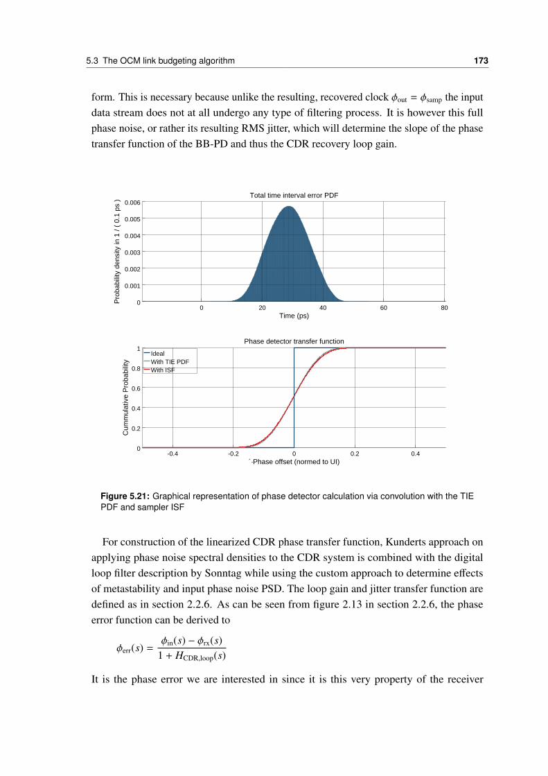
5.3 The OCM link budgeting algorithm 173
form. This is necessary because unlike the resulting, recovered clock φout = φsamp the inputdata stream does not at all undergo any type of filtering process. It is however this fullphase noise, or rather its resulting RMS jitter, which will determine the slope of the phasetransfer function of the BB-PD and thus the CDR recovery loop gain.
0 20 40 60 800
0.001
0.002
0.003
0.004
0.005
0.006
Time (ps)
Pro
babi
lity
dens
ity in
1 /
( 0.
1 ps
)
-0.4 -0.2 0 0.2 0.40
0.2
0.4
0.6
0.8
1
´·Phase offset (normed to UI)
Cum
mul
ativ
e P
roba
bilit
y
IdealWith TIE PDFWith ISF
Total time interval error PDF
Phase detector transfer function
Figure 5.21: Graphical representation of phase detector calculation via convolution with the TIEPDF and sampler ISF
For construction of the linearized CDR phase transfer function, Kunderts approach onapplying phase noise spectral densities to the CDR system is combined with the digitalloop filter description by Sonntag while using the custom approach to determine effectsof metastability and input phase noise PSD. The loop gain and jitter transfer function aredefined as in section 2.2.6. As can be seen from figure 2.13 in section 2.2.6, the phaseerror function can be derived to
φerr(s) =φin(s) − φrx(s)
1 + HCDR,loop(s)
It is the phase error we are interested in since it is this very property of the receiver
174 5 Link budgeting
system that gives timing jitter on the input data stream its meaning - it is the quantity,that the BB-PD will eventually convert to an average digital representation and it is thisrepresentation which will be filtered and used as an estimate of the phase of the incomingclock embedded in the data stream. Now though, this phase error actually is affected bythe CDR loop filtering properties. The input phase noise and the RX reference clock phasenoise power spectral densities are the known quantities and the resulting phase error powerspectral density can consequently be derived to
S φerrφerr(ω) =S φinφin(ω) + S φrxφrx(ω)
1 + H2CDR,loop(ω)
A phase noise spectral density plot as resulting from this filtering process is shown infigure 5.22 where the CDR can be seen to effectively remove the spectral content up tofrequencies set by its own loop bandwidth. It is shown without PI dither contribution. Toits top, the resulting time interval error PDF as required to construct the final, statisticaleye for system metric evaluation is also presented.
While not impossible to estimate, S φrxφrx(ω) is tough to thoroughly model. Apart from theinitial phase noise of the PLL, the entire clock distribution tree with the rather complicatedchain of clock buffers and shapers in the DPC would need to be modeled and its modelparameters estimated. The framework would generally support this procedure as describedin section 2.2.5. On the other hand, as a starting point in design space explorations or forreasons of simplicity, an upper bound estimation may also be used. Once the schematicbased implementation has reached a mature state, a PXF and periodic noise analysis canthen be used to derive the then rather exact form of the receiver reference clock phasenoise.
As explained above, the input data stream phase noise has far more contributors to itsoverall shape. The previous sections already explained the shaping process of the PLL/TXoutput phase noise by the channel and jitter amplification in the presence of reflectionsand equalization. It must be noted here, that estimating the phase noise at the input of thephase detector should not include the equalization effects of the DFE in cases when thereis no feedback summation stage feeding the inputs of the edge samplers. Whether it isworth the additional effort of feedback-equalizing a signal transition, which kind of clocktiming would need to be used for this and also which consequences this may have for theoverall CDR loop dynamics are all questions beyond the scope of this text and open forexploration with the framework presented here.
Finally, digital implementations of clock data recovery circuits do not simply implementa single value for the proportional and integral gain. They can and should be adjustable bydigital control vectors. If such vectors are present, the numeric optimization routines ofOctave and its OCM extension can be used to advise on optimal settings for these vectorswith respect to the overall residual phase noise level for clock recovery.

5.3 The OCM link budgeting algorithm 175
-4 -3 -2 -1 0 10
0.02
0.04
0.06
0.08
Time (ps)
Pro
babi
lity
dens
ity in
1 /
( 0.
1 ps
)
1e-4 1e-3 1e-2 1e-1 1e+0 1e+1-180
-160
-140
-120
-100
-80
Frequency (GHz)
Pow
er S
pect
ral D
ensi
ty d
BC
RX input pnoise PSDCDR REC CLK pnoise PSD
Effective random sampling input TIE PDF after filtering with PI dither
Filtered and unfiltered RX phase noise PSD (without PI dither)
Figure 5.22: TIE PDF as well as unfiltered and filtered sampler input phase noise PSDs resultingfrom analysis procedure presented here
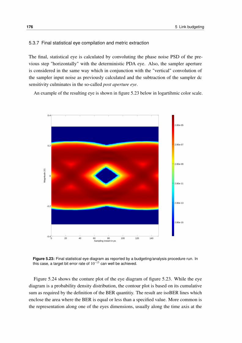
176 5 Link budgeting
5.3.7 Final statistical eye compilation and metric extraction
The final, statistical eye is calculated by convoluting the phase noise PSD of the pre-vious step "horizontally" with the deterministic PDA eye. Also, the sampler apertureis considered in the same way which in conjunction with the "vertical" convolution ofthe sampler input noise as previously calculated and the subtraction of the sampler dcsensitivity culminates in the so-called post aperture eye.
An example of the resulting eye is shown in figure 5.23 below in logartihmic color scale.
0 20 40 60 80 100 120 140-0.4
-0.2
0
0.2
0.4
Sampling instant in ps
Mag
nitu
de (
V)
2.80e-05
2.80e-07
2.80e-09
2.80e-11
2.80e-13
2.80e-15
Figure 5.23: Final statistical eye diagram as reported by a budgeting/analysis procedure run. Inthis case, a target bit error rate of 10−15 can well be achieved.
Figure 5.24 shows the conture plot of the eye diagram of figure 5.23. While the eyediagram is a probability density distribution, the contour plot is based on its cumulativesum as required by the definition of the BER quantitiy. The result are isoBER lines whichenclose the area where the BER is equal or less than a specified value. More common isthe representation along one of the eyes dimensions, usually along the time axis at the
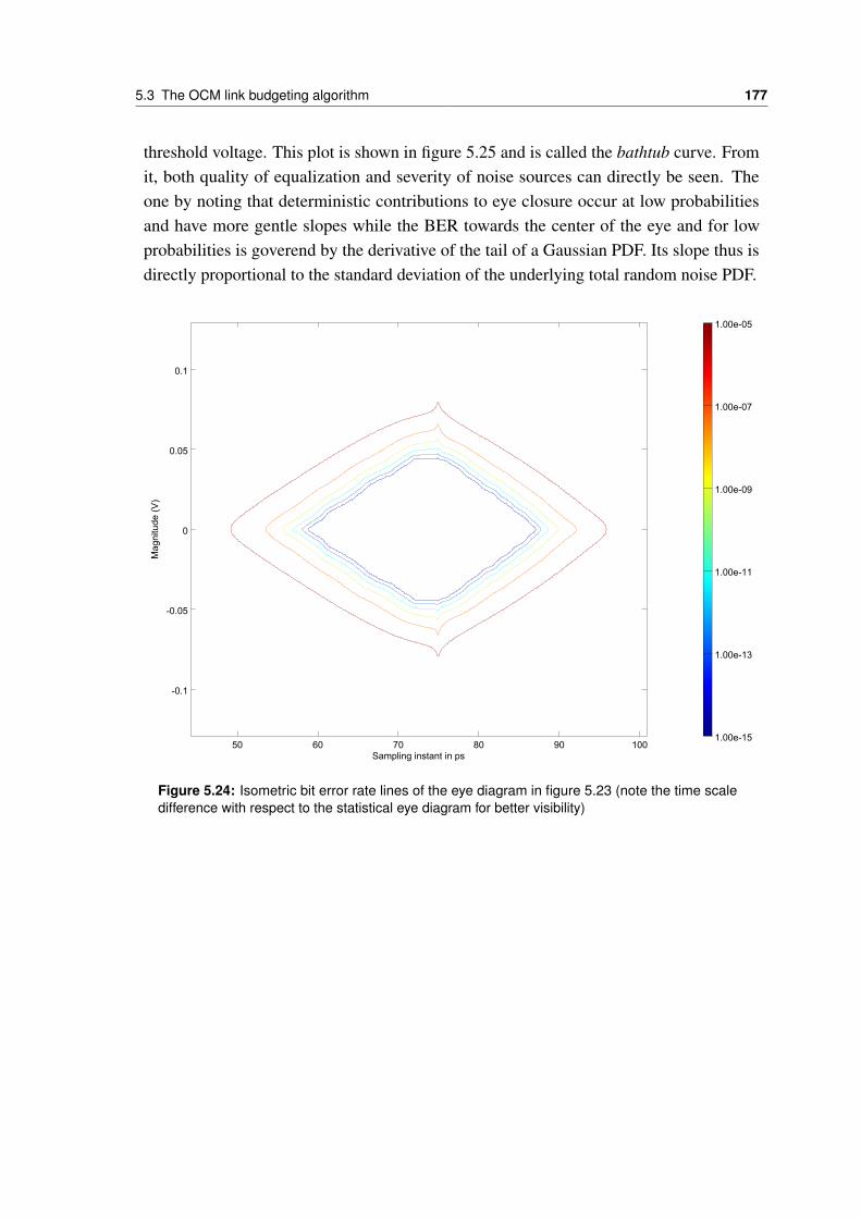
5.3 The OCM link budgeting algorithm 177
threshold voltage. This plot is shown in figure 5.25 and is called the bathtub curve. Fromit, both quality of equalization and severity of noise sources can directly be seen. Theone by noting that deterministic contributions to eye closure occur at low probabilitiesand have more gentle slopes while the BER towards the center of the eye and for lowprobabilities is goverend by the derivative of the tail of a Gaussian PDF. Its slope thus isdirectly proportional to the standard deviation of the underlying total random noise PDF.
50 60 70 80 90 100
-0.1
-0.05
0
0.05
0.1
Sampling instant in ps
Mag
nitu
de (
V)
1.00e-05
1.00e-07
1.00e-09
1.00e-11
1.00e-13
1.00e-15
Figure 5.24: Isometric bit error rate lines of the eye diagram in figure 5.23 (note the time scaledifference with respect to the statistical eye diagram for better visibility)
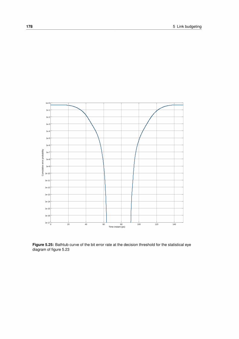
178 5 Link budgeting
0 20 40 60 80 100 120 1401e-17
1e-16
1e-15
1e-14
1e-13
1e-12
1e-11
1e-10
1e-9
1e-8
1e-7
1e-6
1e-5
1e-4
1e-3
1e-2
1e-1
1e+0
Time instant (ps)
Cum
ulat
ive
erro
r pr
obab
ility
Figure 5.25: Bathtub curve of the bit error rate at the decision threshold for the statistical eyediagram of figure 5.23
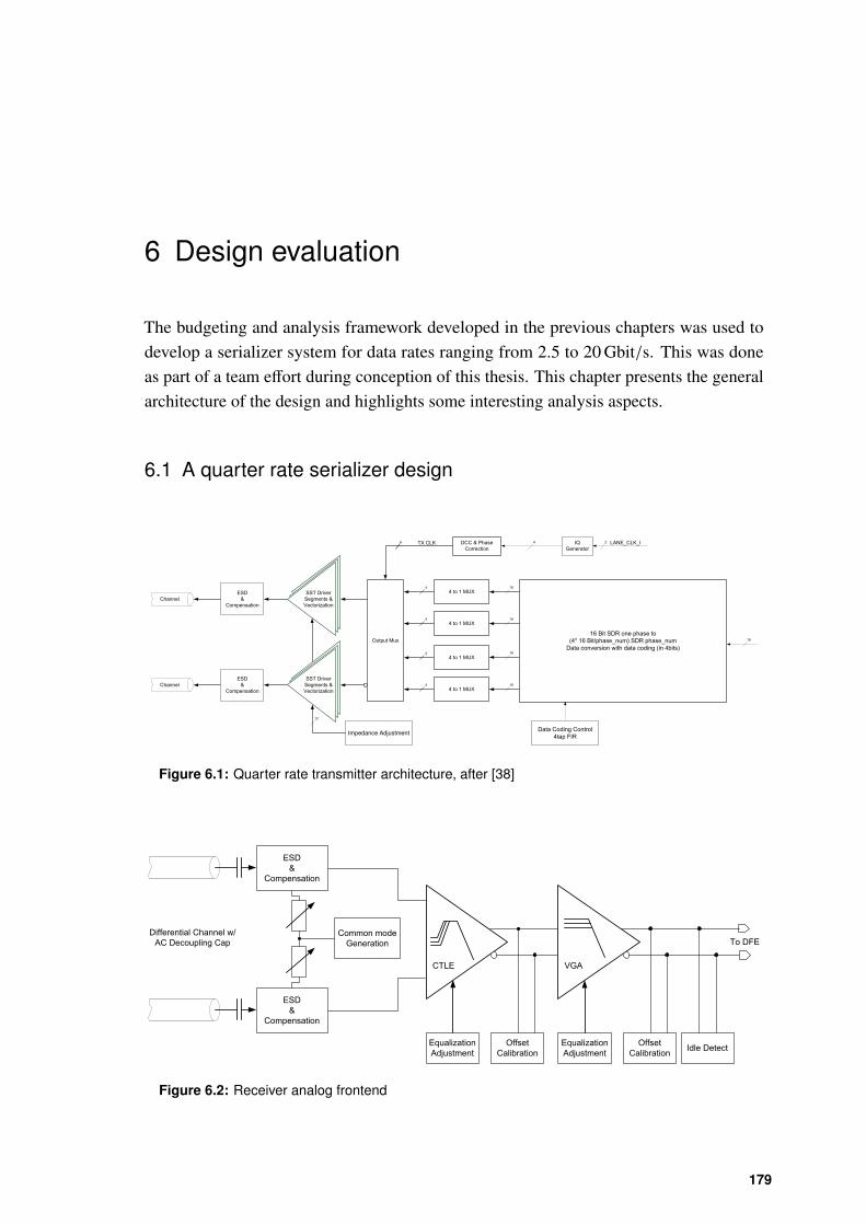
6 Design evaluation
The budgeting and analysis framework developed in the previous chapters was used todevelop a serializer system for data rates ranging from 2.5 to 20 Gbit/s. This was doneas part of a team effort during conception of this thesis. This chapter presents the generalarchitecture of the design and highlights some interesting analysis aspects.
6.1 A quarter rate serializer design
Impedance Adjustment
ChannelESD
&Compensation
4 TX CLK DCC & Phase Correction
IQGenerator
4 LANE_CLK_I2
4
4
4
4
4 to 1 MUX
12
4 to 1 MUX
4 to 1 MUX
4 to 1 MUX
16 Bit SDR one phase to(4* 16 Bit/phase_num) SDR phase_num
Data conversion with data coding (in 4bits)
Data Coding Control4tap FIR
16
16
16
16
16
Output Mux
SST DriverSegments &Vectorization
ChannelESD
&Compensation
SST DriverSegments &Vectorization
Figure 6.1: Quarter rate transmitter architecture, after [38]
ESD &
Compensation
Common mode Generation
Offset Calibration
Idle Detect
Differential Channel w/AC Decoupling Cap
ESD &
Compensation
CTLE
EqualizationAdjustment
VGA
Offset Calibration
EqualizationAdjustment
To DFE
Figure 6.2: Receiver analog frontend
179
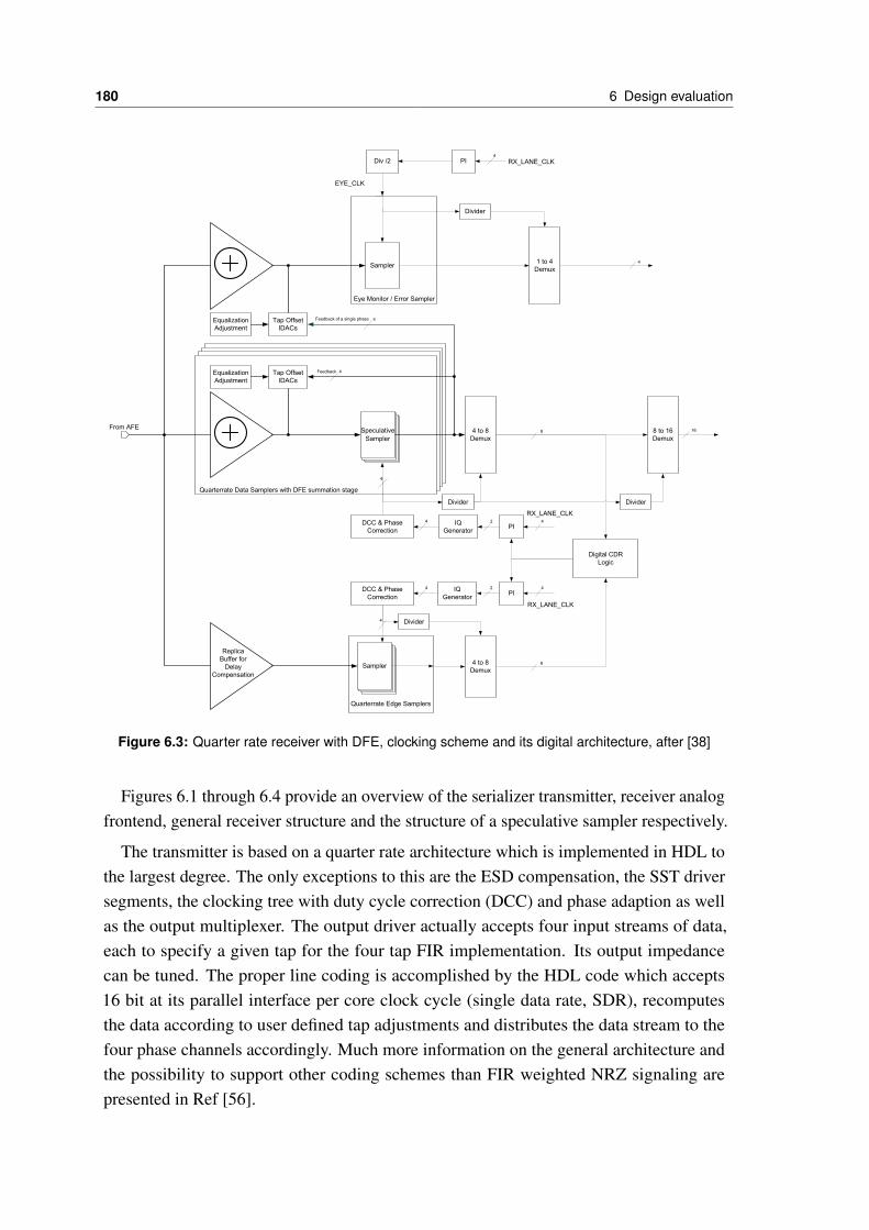
180 6 Design evaluation
IQGenerator
PI4 2 4
4 to 8Demux
PI4
16
EYE_CLK
4
DCC & Phase Correction
Sampler
4
Divider
Quarterrate Data Samplers with DFE summation stage
Sampler
Eye Monitor / Error Sampler
1 to 4Demux
RX_LANE_CLK
SamplerSampler
Divider
RX_LANE_CLKDiv /2
4 to 8Demux
8
Divider
IQGenerator
PI4 2 4DCC & Phase
Correction
4
8 to 16Demux
Divider
Sampler
Quarterrate Edge Samplers
SamplerSamplerSampler
8
RX_LANE_CLK
Digital CDRLogic
Tap Offset IDACs
EqualizationAdjustment
Feedback 4
Tap Offset IDACs
EqualizationAdjustment
4Feedback of a single phase
ReplicaBuffer for
DelayCompensation
From AFE SpeculativeSampler
Figure 6.3: Quarter rate receiver with DFE, clocking scheme and its digital architecture, after [38]
Figures 6.1 through 6.4 provide an overview of the serializer transmitter, receiver analogfrontend, general receiver structure and the structure of a speculative sampler respectively.
The transmitter is based on a quarter rate architecture which is implemented in HDL tothe largest degree. The only exceptions to this are the ESD compensation, the SST driversegments, the clocking tree with duty cycle correction (DCC) and phase adaption as wellas the output multiplexer. The output driver actually accepts four input streams of data,each to specify a given tap for the four tap FIR implementation. Its output impedancecan be tuned. The proper line coding is accomplished by the HDL code which accepts16 bit at its parallel interface per core clock cycle (single data rate, SDR), recomputesthe data according to user defined tap adjustments and distributes the data stream to thefour phase channels accordingly. Much more information on the general architecture andthe possibility to support other coding schemes than FIR weighted NRZ signaling arepresented in Ref [56].
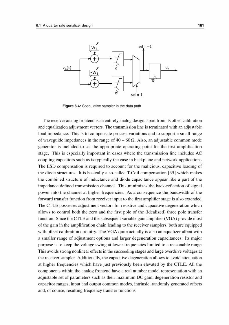
6.1 A quarter rate serializer design 181
φ
+φ
w1
vin(t) dn
sel n-1
+φ
-w1
sel n+1
Figure 6.4: Speculative sampler in the data path
The receiver analog frontend is an entirely analog design, apart from its offset calibrationand equalization adjustment vectors. The transmission line is terminated with an adjustableload impedance. This is to compensate process variations and to support a small rangeof waveguide impedances in the range of 40 − 60Ω. Also, an adjustable common modegenerator is included to set the appropriate operating point for the first amplificationstage. This is especially important in cases where the transmission line includes ACcoupling capacitors such as is typically the case in backplane and network applications.The ESD compensation is required to account for the malicious, capacitive loading ofthe diode structures. It is basically a so-called T-Coil compensation [35] which makesthe combined structure of inductance and diode capacitance appear like a part of theimpedance defined transmission channel. This minimizes the back-reflection of signalpower into the channel at higher frequencies. As a consequence the bandwidth of theforward transfer function from receiver input to the first amplifier stage is also extended.The CTLE possesses adjustment vectors for resistive and capacitive degeneration whichallows to control both the zero and the first pole of the (idealized) three pole transferfunction. Since the CTLE and the subsequent variable gain amplifier (VGA) provide mostof the gain in the amplification chain leading to the receiver samplers, both are equippedwith offset calibration circuitry. The VGA quite actually is also an equalizer albeit witha smaller range of adjustment options and larger degeneration capacitances. Its majorpurpose is to keep the voltage swing at lower frequencies limited to a reasonable range.This avoids strong nonlinear effects in the succeeding stages and large overdrive voltages atthe receiver sampler. Additionally, the capacitive degeneration allows to avoid attenuationat higher frequencies which have just previously been elevated by the CTLE. All thecomponents within the analog frontend have a real number model representation with anadjustable set of parameters such as their maximum DC gain, degeneration resistor andcapacitor ranges, input and output common modes, intrinsic, randomly generated offsetsand, of course, resulting frequency transfer functions.
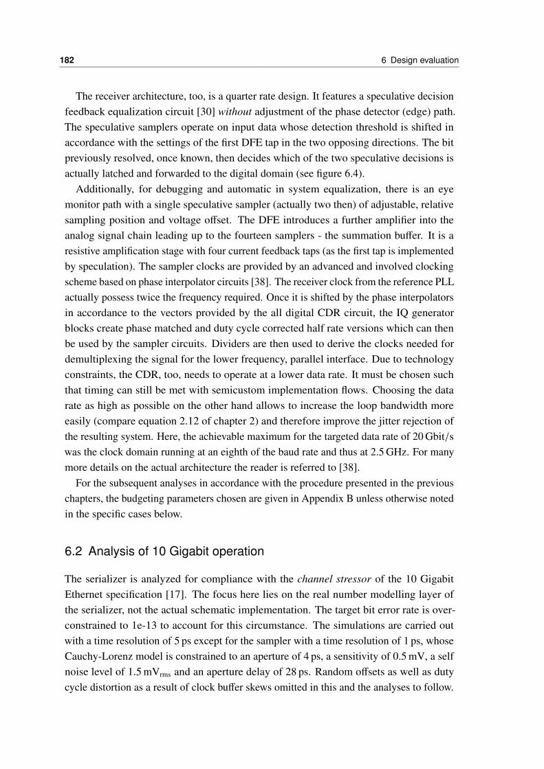
182 6 Design evaluation
The receiver architecture, too, is a quarter rate design. It features a speculative decisionfeedback equalization circuit [30] without adjustment of the phase detector (edge) path.The speculative samplers operate on input data whose detection threshold is shifted inaccordance with the settings of the first DFE tap in the two opposing directions. The bitpreviously resolved, once known, then decides which of the two speculative decisions isactually latched and forwarded to the digital domain (see figure 6.4).
Additionally, for debugging and automatic in system equalization, there is an eyemonitor path with a single speculative sampler (actually two then) of adjustable, relativesampling position and voltage offset. The DFE introduces a further amplifier into theanalog signal chain leading up to the fourteen samplers - the summation buffer. It is aresistive amplification stage with four current feedback taps (as the first tap is implementedby speculation). The sampler clocks are provided by an advanced and involved clockingscheme based on phase interpolator circuits [38]. The receiver clock from the reference PLLactually possess twice the frequency required. Once it is shifted by the phase interpolatorsin accordance to the vectors provided by the all digital CDR circuit, the IQ generatorblocks create phase matched and duty cycle corrected half rate versions which can thenbe used by the sampler circuits. Dividers are then used to derive the clocks needed fordemultiplexing the signal for the lower frequency, parallel interface. Due to technologyconstraints, the CDR, too, needs to operate at a lower data rate. It must be chosen suchthat timing can still be met with semicustom implementation flows. Choosing the datarate as high as possible on the other hand allows to increase the loop bandwidth moreeasily (compare equation 2.12 of chapter 2) and therefore improve the jitter rejection ofthe resulting system. Here, the achievable maximum for the targeted data rate of 20 Gbit/swas the clock domain running at an eighth of the baud rate and thus at 2.5 GHz. For manymore details on the actual architecture the reader is referred to [38].
For the subsequent analyses in accordance with the procedure presented in the previouschapters, the budgeting parameters chosen are given in Appendix B unless otherwise notedin the specific cases below.
6.2 Analysis of 10 Gigabit operation
The serializer is analyzed for compliance with the channel stressor of the 10 GigabitEthernet specification [17]. The focus here lies on the real number modelling layer ofthe serializer, not the actual schematic implementation. The target bit error rate is over-constrained to 1e-13 to account for this circumstance. The simulations are carried outwith a time resolution of 5 ps except for the sampler with a time resolution of 1 ps, whoseCauchy-Lorenz model is constrained to an aperture of 4 ps, a sensitivity of 0.5 mV, a selfnoise level of 1.5 mVrms and an aperture delay of 28 ps. Random offsets as well as dutycycle distortion as a result of clock buffer skews omitted in this and the analyses to follow.
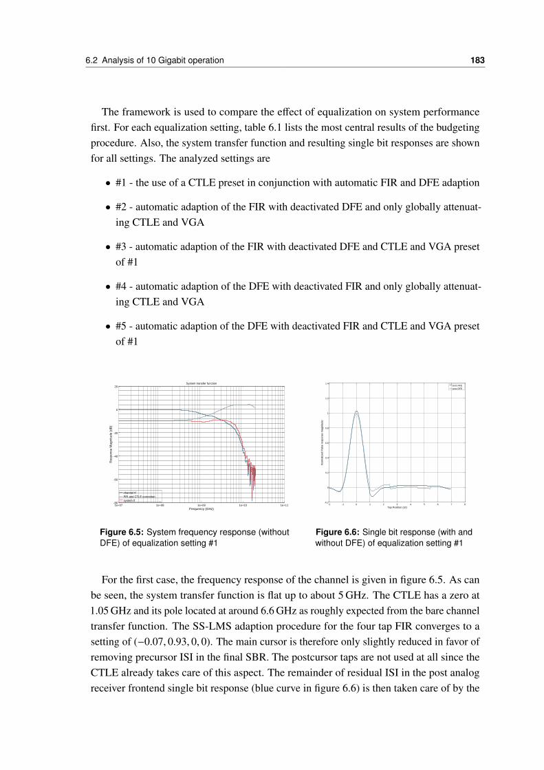
6.2 Analysis of 10 Gigabit operation 183
The framework is used to compare the effect of equalization on system performancefirst. For each equalization setting, table 6.1 lists the most central results of the budgetingprocedure. Also, the system transfer function and resulting single bit responses are shownfor all settings. The analyzed settings are
• #1 - the use of a CTLE preset in conjunction with automatic FIR and DFE adaption
• #2 - automatic adaption of the FIR with deactivated DFE and only globally attenuat-ing CTLE and VGA
• #3 - automatic adaption of the FIR with deactivated DFE and CTLE and VGA presetof #1
• #4 - automatic adaption of the DFE with deactivated FIR and only globally attenuat-ing CTLE and VGA
• #5 - automatic adaption of the DFE with deactivated FIR and CTLE and VGA presetof #1
1e+07 1e+08 1e+09 1e+10 1e+11-80
-60
-40
-20
0
20
Frequency (GHz)
Res
pons
e M
agni
tude
(dB
)
channel tfFIR and CTLE correctionsystem tf
System transfer function
Figure 6.5: System frequency response (withoutDFE) of equalization setting #1
-2 -1 0 1 2 3 4 5 6 7 8-0.2
0
0.2
0.4
0.6
0.8
1
1.2
1.4
Tap Position (UI)
Nor
mal
ized
Pul
se r
espo
nse
mag
nitu
de
post AFEpost DFE
Figure 6.6: Single bit response (with andwithout DFE) of equalization setting #1
For the first case, the frequency response of the channel is given in figure 6.5. As canbe seen, the system transfer function is flat up to about 5 GHz. The CTLE has a zero at1.05 GHz and its pole located at around 6.6 GHz as roughly expected from the bare channeltransfer function. The SS-LMS adaption procedure for the four tap FIR converges to asetting of (−0.07, 0.93, 0, 0). The main cursor is therefore only slightly reduced in favor ofremoving precursor ISI in the final SBR. The postcursor taps are not used at all since theCTLE already takes care of this aspect. The remainder of residual ISI in the post analogreceiver frontend single bit response (blue curve in figure 6.6) is then taken care of by the
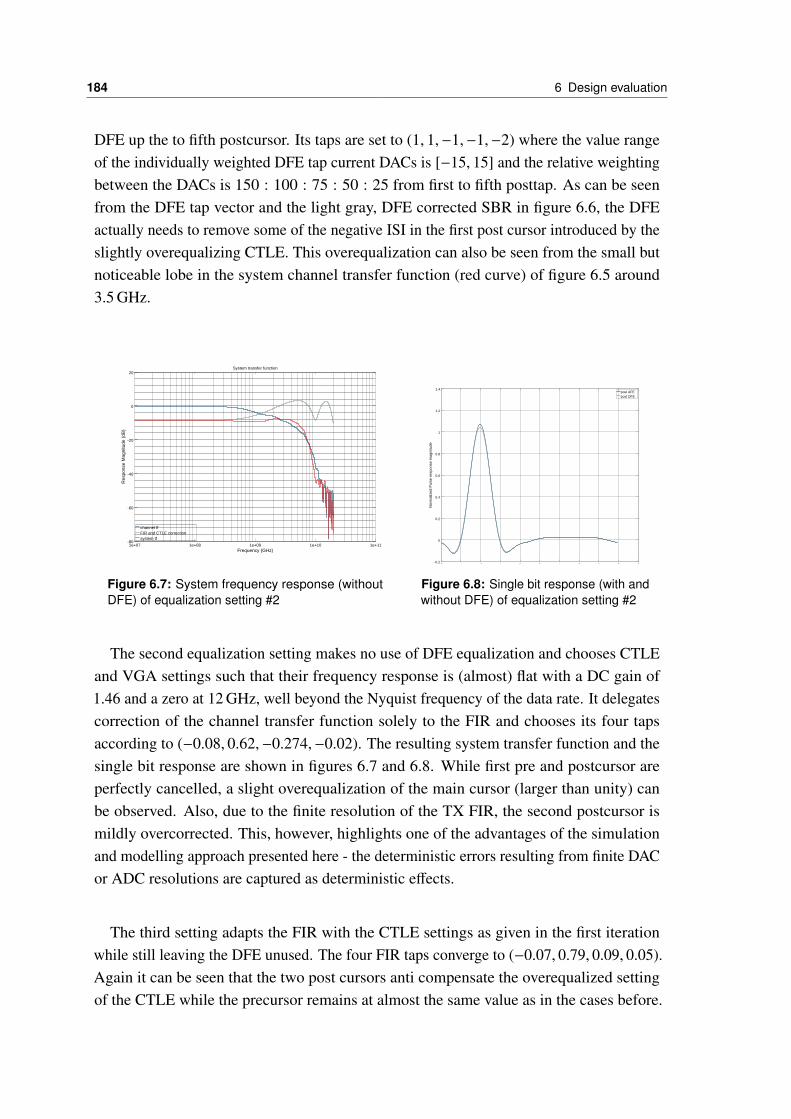
184 6 Design evaluation
DFE up the to fifth postcursor. Its taps are set to (1, 1,−1,−1,−2) where the value rangeof the individually weighted DFE tap current DACs is [−15, 15] and the relative weightingbetween the DACs is 150 : 100 : 75 : 50 : 25 from first to fifth posttap. As can be seenfrom the DFE tap vector and the light gray, DFE corrected SBR in figure 6.6, the DFEactually needs to remove some of the negative ISI in the first post cursor introduced by theslightly overequalizing CTLE. This overequalization can also be seen from the small butnoticeable lobe in the system channel transfer function (red curve) of figure 6.5 around3.5 GHz.
1e+07 1e+08 1e+09 1e+10 1e+11-80
-60
-40
-20
0
20
Frequency (GHz)
Res
pons
e M
agni
tude
(dB
)
channel tfFIR and CTLE correctionsystem tf
System transfer function
Figure 6.7: System frequency response (withoutDFE) of equalization setting #2
-2 -1 -0 1 2 3 4 5 6 7 8-0.2
0
0.2
0.4
0.6
0.8
1
1.2
1.4
Nor
mal
ized
Pul
se r
espo
nse
mag
nitu
de
post AFEpost DFE
Figure 6.8: Single bit response (with andwithout DFE) of equalization setting #2
The second equalization setting makes no use of DFE equalization and chooses CTLEand VGA settings such that their frequency response is (almost) flat with a DC gain of1.46 and a zero at 12 GHz, well beyond the Nyquist frequency of the data rate. It delegatescorrection of the channel transfer function solely to the FIR and chooses its four tapsaccording to (−0.08, 0.62,−0.274,−0.02). The resulting system transfer function and thesingle bit response are shown in figures 6.7 and 6.8. While first pre and postcursor areperfectly cancelled, a slight overequalization of the main cursor (larger than unity) canbe observed. Also, due to the finite resolution of the TX FIR, the second postcursor ismildly overcorrected. This, however, highlights one of the advantages of the simulationand modelling approach presented here - the deterministic errors resulting from finite DACor ADC resolutions are captured as deterministic effects.
The third setting adapts the FIR with the CTLE settings as given in the first iterationwhile still leaving the DFE unused. The four FIR taps converge to (−0.07, 0.79, 0.09, 0.05).Again it can be seen that the two post cursors anti compensate the overequalized settingof the CTLE while the precursor remains at almost the same value as in the cases before.

6.2 Analysis of 10 Gigabit operation 185
1e+07 1e+08 1e+09 1e+10 1e+11-80
-60
-40
-20
0
20
Frequency (GHz)
Res
pons
e M
agni
tude
(dB
)
channel tfFIR and CTLE correctionsystem tf
System transfer function
Figure 6.9: System frequency response (withoutDFE) of equalization setting #3
-2 -1 0 1 2 3 4 5 6 7 8-0.2
0
0.2
0.4
0.6
0.8
1
1.2
1.4
Tap Position (UI)
Nor
mal
ized
Pul
se r
espo
nse
mag
nitu
de
post AFEpost DFE
Figure 6.10: Single bit response (withand without DFE) of equalization setting#3
From table 6.1 it can be seen that this effectively trades eye height against an increase ineye width. As can be seen from figure 6.10, the overequalization of the main cursor isremoved and the second post cursor manages to nearly zero out the ISI at its location. As aconsequence, the system frequency transfer functions flatness is superior to those of thepreceding examples.
1e+07 1e+08 1e+09 1e+10 1e+11-80
-60
-40
-20
0
20
Frequency (GHz)
Res
pons
e M
agni
tude
(dB
)
channel tfFIR and CTLE correctionsystem tf
System transfer function
Figure 6.11: System frequency response (withoutDFE) of equalization setting #4
-2 -1 0 1 2 3 4 5 6 7 8-0.2
0
0.2
0.4
0.6
0.8
Tap Position (UI)
Nor
mal
ized
Pul
se r
espo
nse
mag
nitu
de
post AFEpost DFE
Figure 6.12: Single bit response (withand without DFE) of equalization setting#4
The fourth setting uses neither FIR nor CTLE (apart from a signal gain of 1.46). As aresult, the system transfer function without DFE is unchanged in shape, the resulting singlebit response after the receiver analog frontend exhibits large magnitudes of ISI which arecompletely cancelled by the first speculative and second, current DAC based tap. TheDFE tap weights which the SS-LMS algorithm converges to are (−15,−12,−9,−8,−7). Itis unclear why the last taps do not converge to more negative values as the tuning range
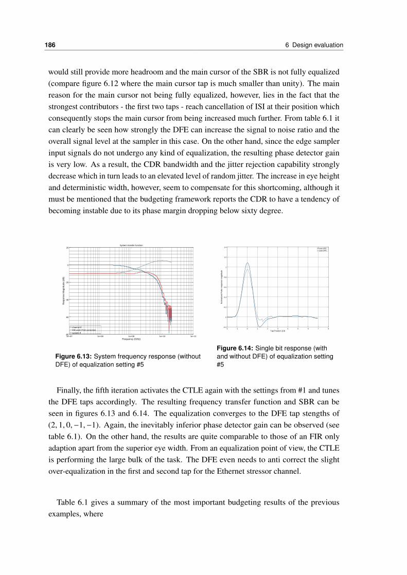
186 6 Design evaluation
would still provide more headroom and the main cursor of the SBR is not fully equalized(compare figure 6.12 where the main cursor tap is much smaller than unity). The mainreason for the main cursor not being fully equalized, however, lies in the fact that thestrongest contributors - the first two taps - reach cancellation of ISI at their position whichconsequently stops the main cursor from being increased much further. From table 6.1 itcan clearly be seen how strongly the DFE can increase the signal to noise ratio and theoverall signal level at the sampler in this case. On the other hand, since the edge samplerinput signals do not undergo any kind of equalization, the resulting phase detector gainis very low. As a result, the CDR bandwidth and the jitter rejection capability stronglydecrease which in turn leads to an elevated level of random jitter. The increase in eye heightand deterministic width, however, seem to compensate for this shortcoming, although itmust be mentioned that the budgeting framework reports the CDR to have a tendency ofbecoming instable due to its phase margin dropping below sixty degree.
1e+07 1e+08 1e+09 1e+10 1e+11-80
-60
-40
-20
0
20
Frequency (GHz)
Res
pons
e M
agni
tude
(dB
)
channel tfFIR and CTLE correctionsystem tf
System transfer function
Figure 6.13: System frequency response (withoutDFE) of equalization setting #5
-2 -1 0 1 2 3 4 5 6 7 8-0.2
0
0.2
0.4
0.6
0.8
1
1.2
1.4
Tap Position (UI)
Nor
mal
ized
Pul
se r
espo
nse
mag
nitu
de
post AFEpost DFE
Figure 6.14: Single bit response (withand without DFE) of equalization setting#5
Finally, the fifth iteration activates the CTLE again with the settings from #1 and tunesthe DFE taps accordingly. The resulting frequency transfer function and SBR can beseen in figures 6.13 and 6.14. The equalization converges to the DFE tap stengths of(2, 1, 0,−1,−1). Again, the inevitably inferior phase detector gain can be observed (seetable 6.1). On the other hand, the results are quite comparable to those of an FIR onlyadaption apart from the superior eye width. From an equalization point of view, the CTLEis performing the large bulk of the task. The DFE even needs to anti correct the slightover-equalization in the first and second tap for the Ethernet stressor channel.
Table 6.1 gives a summary of the most important budgeting results of the previousexamples, where
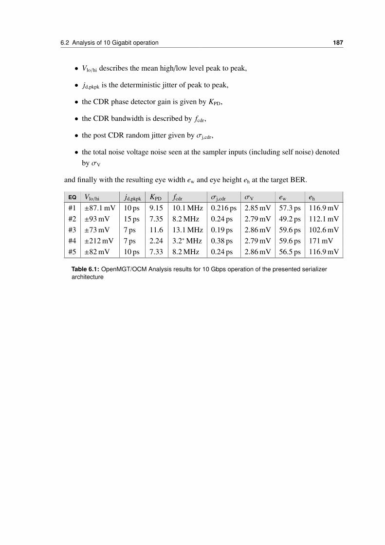
6.2 Analysis of 10 Gigabit operation 187
• Vlo/hi describes the mean high/low level peak to peak,
• jd,pkpk is the deterministic jitter of peak to peak,
• the CDR phase detector gain is given by KPD,
• the CDR bandwidth is described by fcdr,
• the post CDR random jitter given by σj,cdr,
• the total noise voltage noise seen at the sampler inputs (including self noise) denotedby σV
and finally with the resulting eye width ew and eye height eh at the target BER.
EQ Vlo/hi jd,pkpk KPD fcdr σj,cdr σV ew eh
#1 ±87.1 mV 10 ps 9.15 10.1 MHz 0.216 ps 2.85 mV 57.3 ps 116.9 mV#2 ±93 mV 15 ps 7.35 8.2 MHz 0.24 ps 2.79 mV 49.2 ps 112.1 mV#3 ±73 mV 7 ps 11.6 13.1 MHz 0.19 ps 2.86 mV 59.6 ps 102.6 mV#4 ±212 mV 7 ps 2.24 3.2∗MHz 0.38 ps 2.79 mV 59.6 ps 171 mV#5 ±82 mV 10 ps 7.33 8.2 MHz 0.24 ps 2.86 mV 56.5 ps 116.9 mV
Table 6.1: OpenMGT/OCM Analysis results for 10 Gbps operation of the presented serializerarchitecture
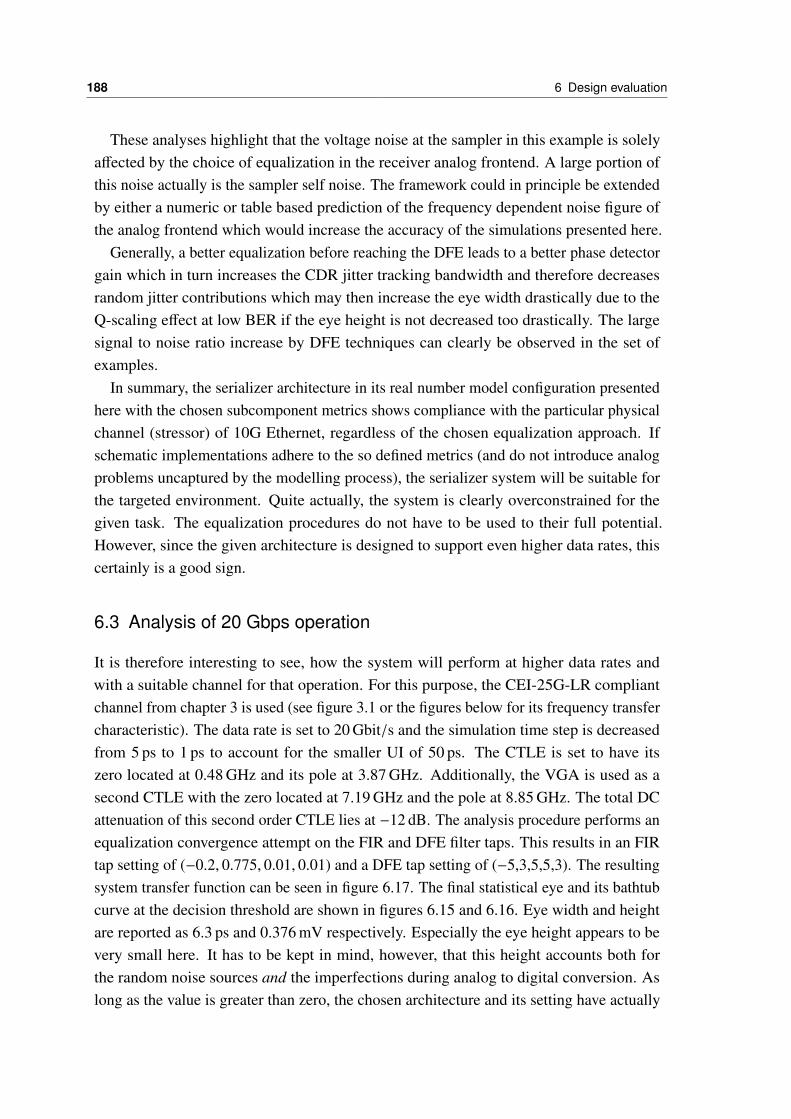
188 6 Design evaluation
These analyses highlight that the voltage noise at the sampler in this example is solelyaffected by the choice of equalization in the receiver analog frontend. A large portion ofthis noise actually is the sampler self noise. The framework could in principle be extendedby either a numeric or table based prediction of the frequency dependent noise figure ofthe analog frontend which would increase the accuracy of the simulations presented here.
Generally, a better equalization before reaching the DFE leads to a better phase detectorgain which in turn increases the CDR jitter tracking bandwidth and therefore decreasesrandom jitter contributions which may then increase the eye width drastically due to theQ-scaling effect at low BER if the eye height is not decreased too drastically. The largesignal to noise ratio increase by DFE techniques can clearly be observed in the set ofexamples.
In summary, the serializer architecture in its real number model configuration presentedhere with the chosen subcomponent metrics shows compliance with the particular physicalchannel (stressor) of 10G Ethernet, regardless of the chosen equalization approach. Ifschematic implementations adhere to the so defined metrics (and do not introduce analogproblems uncaptured by the modelling process), the serializer system will be suitable forthe targeted environment. Quite actually, the system is clearly overconstrained for thegiven task. The equalization procedures do not have to be used to their full potential.However, since the given architecture is designed to support even higher data rates, thiscertainly is a good sign.
6.3 Analysis of 20 Gbps operation
It is therefore interesting to see, how the system will perform at higher data rates andwith a suitable channel for that operation. For this purpose, the CEI-25G-LR compliantchannel from chapter 3 is used (see figure 3.1 or the figures below for its frequency transfercharacteristic). The data rate is set to 20 Gbit/s and the simulation time step is decreasedfrom 5 ps to 1 ps to account for the smaller UI of 50 ps. The CTLE is set to have itszero located at 0.48 GHz and its pole at 3.87 GHz. Additionally, the VGA is used as asecond CTLE with the zero located at 7.19 GHz and the pole at 8.85 GHz. The total DCattenuation of this second order CTLE lies at −12 dB. The analysis procedure performs anequalization convergence attempt on the FIR and DFE filter taps. This results in an FIRtap setting of (−0.2, 0.775, 0.01, 0.01) and a DFE tap setting of (−5,3,5,5,3). The resultingsystem transfer function can be seen in figure 6.17. The final statistical eye and its bathtubcurve at the decision threshold are shown in figures 6.15 and 6.16. Eye width and heightare reported as 6.3 ps and 0.376 mV respectively. Especially the eye height appears to bevery small here. It has to be kept in mind, however, that this height accounts both forthe random noise sources and the imperfections during analog to digital conversion. Aslong as the value is greater than zero, the chosen architecture and its setting have actually
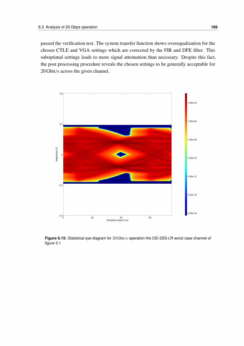
6.3 Analysis of 20 Gbps operation 189
passed the verification test. The system transfer function shows overequalization for thechosen CTLE and VGA settings which are corrected by the FIR and DFE filter. Thissuboptimal settings leads to more signal attenuation than necessary. Despite this fact,the post processing procedure reveals the chosen settings to be generally acceptable for20 Gbit/s across the given channel.
0 20 40 60-0.4
-0.2
0
0.2
0.4
Sampling instant in ps
Mag
nitu
de (
V)
1.90e-04
1.90e-06
1.90e-08
1.90e-10
1.90e-12
1.90e-14
1.90e-16
Figure 6.15: Statistical eye diagram for 20 Gbit/s operation the CEI-25G-LR worst case channel offigure 3.1
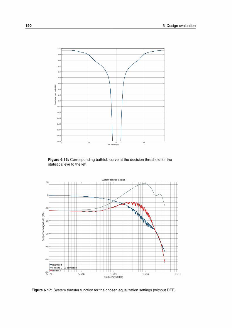
190 6 Design evaluation
0 20 40 601e-16
1e-15
1e-14
1e-13
1e-12
1e-11
1e-10
1e-9
1e-8
1e-7
1e-6
1e-5
1e-4
1e-3
1e-2
1e-1
1e+0
Time instant (ps)
Cum
ulat
ive
erro
r pr
obab
ility
Figure 6.16: Corresponding bathtub curve at the decision threshold for thestatistical eye to the left
1e+07 1e+08 1e+09 1e+10 1e+11-60
-50
-40
-30
-20
-10
0
10
Frequency (GHz)
Res
pons
e M
agni
tude
(dB
)
channel tfFIR and CTLE correctionsystem tf
System transfer function
Figure 6.17: System transfer function for the chosen equalization settings (without DFE)

6.4 Influence of the sampler ISF 191
6.4 Influence of the sampler ISF
The major aim of developing the framework presented here is twofold. First, it shall beused to verify the functional correctness and specification conformity of serializer systems.The previous section highlighted some aspects of this process with respect to equalizationprovisioning and choices. The second goal, however, is to also allow for fast design spaceexploration as a tool for future serializer designs. As an example, the influence of thereceiver sampler aperture on overall system performance will exemplify this aspect of theframework.
The same simulation as carried out in setting #1 is repeated here, only this time theaperture is decreased from the 4 ps of the previous version to 8 ps. This degradation ofsampler aperture might for instance result from an IR drop on the supply or, as shownin section 4.5, due to lowered rise and fall times of the clock signal as they typicallyresult from additional capacitive load on the clock tree (i.e. as a result of the post layoutextraction) or from insufficient capacitive decoupling of the CMOS clock buffers.
Table 6.2 summarizes the results from the previous and this new simulation run.
Aperture Vlo/hi jd,pk−pk KPD fcdr σj,cdr ew eh
4 ps ±87.1 mV 10 ps 9.15 10.1 MHz 0.216 ps 57.3 ps 116.9 mV8 ps ±87.2 mV 11 ps 8 8.8 MHz 0.231 ps 34.2 ps 80.78 mV
Table 6.2: OpenMGT/OCM Analysis results for 10 Gbps operation of the presented serializerarchitecture
The equalization properties should not and are not affected by the change in aperturewidth as long as the correct bits are still resolved - a property checked by the transientsimulation run itself outside the domain of numeric post processing. However, since theCDR phase detector gain directly depends on the sampler ISF, it consequently decreases toa lower value and with it the CDR bandwidth. This in turn increases the random jitter. Thevoltage noise on the other hand is of course not affected unless the physically reasonablereduction of sampler self noise due to the smaller sampling bandwidth would also betaken into account (which has not been done here). Compared to these mild changes insubcomponent metrics, however, the final statistical, post aperture eye shows a much moresevere degradation, both in vertical and horizontal dimension. The strong decrease ineye width is a consequence of the weighting process of the now broadened aperture. Thepre-aperture eye can be conceived as the eye as evaluated by a Dirac like sampler whilethe post-aperture eye, by convolution, factors in the nonideal voltage resolution processof the sampler. The same argument can be made for the decrease in eye height. The postaperture eye height needs to take into account the contributions of the input voltage atvarious time instants. The post aperture eye thus represents the ISF weighted average ofthe pre-aperture voltages seen over the ISF duration. The resulting iso-BER plots of the
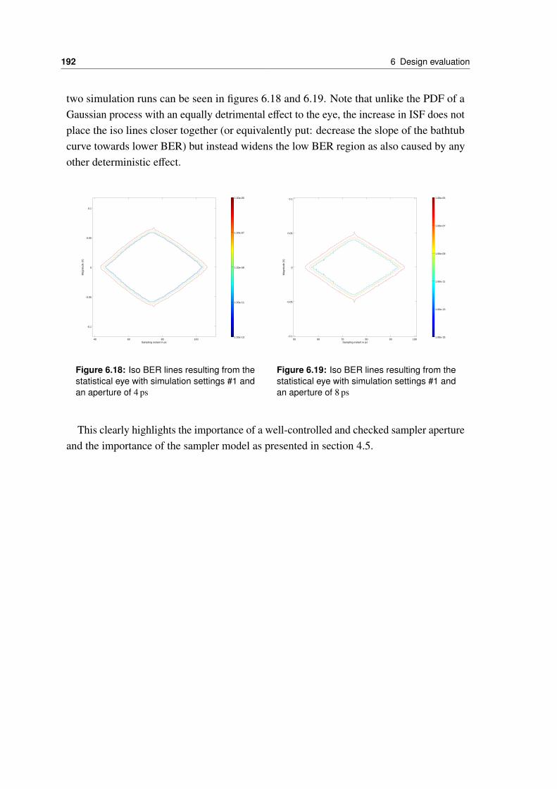
192 6 Design evaluation
two simulation runs can be seen in figures 6.18 and 6.19. Note that unlike the PDF of aGaussian process with an equally detrimental effect to the eye, the increase in ISF does notplace the iso lines closer together (or equivalently put: decrease the slope of the bathtubcurve towards lower BER) but instead widens the low BER region as also caused by anyother deterministic effect.
40 60 80 100
-0.1
-0.05
0
0.05
0.1
Sampling instant in ps
Mag
nitu
de (
V)
1.00e-05
1.00e-07
1.00e-09
1.00e-11
1.00e-13
Figure 6.18: Iso BER lines resulting from thestatistical eye with simulation settings #1 andan aperture of 4 ps
50 60 70 80 90 100-0.1
-0.05
0
0.05
0.1
Sampling instant in ps
Mag
nitu
de (
V)
1.00e-05
1.00e-07
1.00e-09
1.00e-11
1.00e-13
1.00e-15
Figure 6.19: Iso BER lines resulting from thestatistical eye with simulation settings #1 andan aperture of 8 ps
This clearly highlights the importance of a well-controlled and checked sampler apertureand the importance of the sampler model as presented in section 4.5.
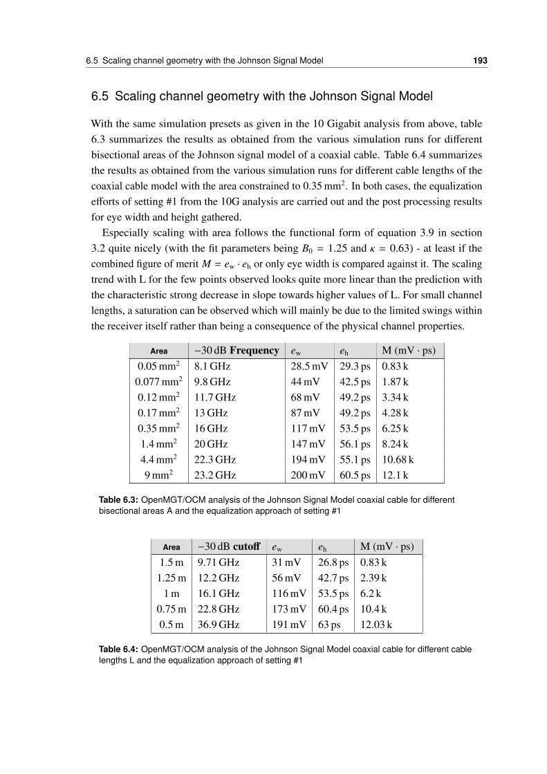
6.5 Scaling channel geometry with the Johnson Signal Model 193
6.5 Scaling channel geometry with the Johnson Signal Model
With the same simulation presets as given in the 10 Gigabit analysis from above, table6.3 summarizes the results as obtained from the various simulation runs for differentbisectional areas of the Johnson signal model of a coaxial cable. Table 6.4 summarizesthe results as obtained from the various simulation runs for different cable lengths of thecoaxial cable model with the area constrained to 0.35 mm2. In both cases, the equalizationefforts of setting #1 from the 10G analysis are carried out and the post processing resultsfor eye width and height gathered.
Especially scaling with area follows the functional form of equation 3.9 in section3.2 quite nicely (with the fit parameters being B0 = 1.25 and κ = 0.63) - at least if thecombined figure of merit M = ew · eh or only eye width is compared against it. The scalingtrend with L for the few points observed looks quite more linear than the prediction withthe characteristic strong decrease in slope towards higher values of L. For small channellengths, a saturation can be observed which will mainly be due to the limited swings withinthe receiver itself rather than being a consequence of the physical channel properties.
Area −30 dB Frequency ew eh M (mV · ps)0.05 mm2 8.1 GHz 28.5 mV 29.3 ps 0.83 k
0.077 mm2 9.8 GHz 44 mV 42.5 ps 1.87 k0.12 mm2 11.7 GHz 68 mV 49.2 ps 3.34 k0.17 mm2 13 GHz 87 mV 49.2 ps 4.28 k0.35 mm2 16 GHz 117 mV 53.5 ps 6.25 k1.4 mm2 20 GHz 147 mV 56.1 ps 8.24 k4.4 mm2 22.3 GHz 194 mV 55.1 ps 10.68 k9 mm2 23.2 GHz 200 mV 60.5 ps 12.1 k
Table 6.3: OpenMGT/OCM analysis of the Johnson Signal Model coaxial cable for differentbisectional areas A and the equalization approach of setting #1
Area −30 dB cutoff ew eh M (mV · ps)1.5 m 9.71 GHz 31 mV 26.8 ps 0.83 k
1.25 m 12.2 GHz 56 mV 42.7 ps 2.39 k1 m 16.1 GHz 116 mV 53.5 ps 6.2 k
0.75 m 22.8 GHz 173 mV 60.4 ps 10.4 k0.5 m 36.9 GHz 191 mV 63 ps 12.03 k
Table 6.4: OpenMGT/OCM analysis of the Johnson Signal Model coaxial cable for different cablelengths L and the equalization approach of setting #1

194 6 Design evaluation
Bisectional Area A (sq mm)
1.4
1.2
1
0.8
0.6
0.4
0.2
01086
Eye widthEye heightFOMFit
420
Nor
mal
ized
mag
nitu
de
Figure 6.20: Normalized eye height, width and figure of merit M versus bisectional area A of theJohnson signal model coaxial cable
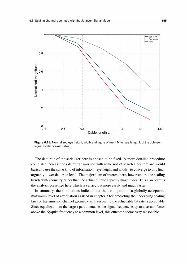
6.5 Scaling channel geometry with the Johnson Signal Model 195
Cable length L (m)
1
0.8
0.6
0.4
0.2
01.61.41.210.8
Eye widthEye heightFOM
0.60.4
Nor
mal
ized
mag
nitu
de
Figure 6.21: Normalized eye height, width and figure of merit M versus length L of the Johnsonsignal model coaxial cable
The data rate of the serializer here is chosen to be fixed. A more detailed procedurecould also increase the rate of transmission with some sort of search algorithm and wouldbasically use the same kind of information - eye height and width - to converge to this final,arguably lower data rate level. The major item of interest here, however, are the scalingtrends with geometry rather than the actual bit rate capacity magnitudes. This also permitsthe analysis presented here which is carried out more easily and much faster.
In summary, the simulations indicate that the assumption of a globally acceptable,maximum level of attenuation as used in chapter 3 for predicting the underlying scalinglaws of transmission channel geometry with respect to the achievable bit rate is acceptable.Since equalization to the largest part attenuates the signal frequencies up to a certain factorabove the Nyquist frequency to a common level, this outcome seems very reasonable.

7 Conclusion and Outlook
This work presented a design and analysis framework for modelling and implementing amultigigabit serializer design. It is based on previously published analysis and modellingideas for the various serializer subcomponents but realizes and combines them in a new andunique way to be compatible with the context of real number model based simulation andverification. The framework strictly separates deterministic and random effects in order tominimize the negative impact of statistical processes on analysis time. Additionally, theansatz implicitly ensures consistency between different modelling views and the actualimplementation of a subcomponent, especially between real number and full-analog realms.Due to the resulting, superior simulation performance, the framework thus allows to analyzea broad range of serializer system properties that were previously intractable by a singledesign and simulation environment.
The strong entanglement of the serializer with higher OSI protocol layers underlined therequirement of having meaningful, accurate, yet very fast simulation models at disposalto allow for higher level integration in larger systems and to enable the development ofcomplex link protocols with automatic equalization support. To this end, the SystemVerilogreal number modelling approach in conjunction with VerilogAMS mixed signal simulationwas used to conceive the openMGT framework in collaboration with another dissertation[38]. Its main ideas are a top-down, digital first implementation approach together with aflexible model view on each system subcomponent. The modelling views can be either ofpurely functional (VerilogHDL), real number signal flow or electrical (SPICE/SPECTRE)nature depending on modelling scope and required accuracy. This mechnism is used to keepmodelling and implementation consistent. It also introduces the concept of interoperabletestbenches for real number and all analog representation which may serve as both ameans of analog component verification and real number model extraction. On the basisof well-established theories, the process was exemplified with the computationally mostchallenging parts of a serializer system: the transmission channel and the high speedreceiver samplers.
By extending the commercial simulation tools with optimized and parallelized customC code, the compuational flexibility of Octave, the SystemVerilog DPI extension andby optimizing the SystemVerilog modelling process, the resulting real number singalflow models simulate approximately a factor of a thousand times faster than their allanalog counterparts while no loss in accuracy with respect to the extracted subcomponent
197
198 7 Conclusion and Outlook
parameters is observed. The modellig infrastructure also allows to use parameterizable,numeric models in order to use the resulting simulation framework for a more generalanalysis of the so-called transmission channel bit rate capacity.
Moreover, the Octave extension to the SystemVerilog openMGT framework via DPI,dubbed OCM, also enables the powerful numeric postprocessing required for serializerbudgeting and design analysis. It provides mathematical algorithms not customarily foundwithin SystemVerilog itself and ways to parallelize vector and matrix based numericcomputation to drastically decrease post processing runtime. OCM therefore not onlyallows the flexible definition of models, but also advanced data acquisition and postprocessing functionality along with a mechanism to keep the model definitions used intransient simulations fully consistent with the data base of post processing analysis.
One particular application to OCM presented here are physical transmission channelsand their bit rate capacity. Channels are very difficult to model, involving many freelyselectable parameters and geometries. This task is therefore often delegated to advanced,commerical microwave engineering software tools. For more comparable analyses inthe context of the bit rate capacity as use in HPC technology projections, the Johnsonsignal model of a coaxial line is presented here as an alternative and implemented in OCM.It allows to capture more physical channel effects than previously and is thus used as abasis for a new projection attempt. Even without considering the serializer system itself,general trends of the bit rate capacity in the multigigabit regime with respect to channelimpedance, bisectional area and length are shown. These results ammend previous workdone in this context. The trends derived indicate a scaling with bisectional area that isless favorable than previously anticipated. It also highlights the optimality of signalling inthe impedance regime around 45 to 60 Ω. On the other hand, it can also be seen that thebit rate capacity may actually downscale less drastically with length than the previouslypostulated, geometric trend.
The design and modelling framework is supplemented by a serializer link budgetingalgorithm. It combines the insights of the foregoing chapters and captures all deterministiceffects of the system such as duty cycle distortion, residual offsets or imperfect equalizationin a transient simulation run. A strict separation of deterministic effects from randomtiming noise and random voltage noise enables fast design space exploration and analysis.The OCM extension allows model data consistency by working within a single toolenvironment only.
The implementation presented in this work is based on the well-known peak distortionalgorithm. It is a statistical analysis to reduce the required transient simulation time by afactor of roughly one million to achieve the same level of statistical eye diagram accuracy.The algorithm is implemented in Octave and uses its above mentioned parallelizationcapabilities to speed up this process.
The budgeting procedure includes effects of timing jitter, voltage noise and a linearized
199
phase state model for the clock recovery circuit to arrive at an estimate for the statisticaleye diagram as it ought to be observed by the receiver. It does so by considering timingjitter entirely in frequency domain (as opposed to time domain descriptions in traditionalapproaches). It also describes the CDR with its phase state model based on well establishedtheory enriched by information otherwise not available to modelling attempts outside ofOCM. This is especially true with respect to sampler performance metrics such as theimpulse sensitivity function or to deterministic jitter resulting from residual intersymbolinterference.
The framework is then used to assess the performance of a serializer design for 10Gigabit Ethernet as it was codeveloped in a team and along with this thesis. Differentoptions of equalization and their effect on overall eye opening are analyzed and thepresented serializer system is shown to be compliant with the 10G Ethernet channel model.
In order to highlight the frameworks capability of supporting design space explorationefforts and the importance of sampler aperture modelling, the impact of the sampler impulsesensitivity function on overall system performance is demonstrated.
Also, the Johnson signal model is used in conjunction with this system to gain morerealistic insight into the scaling properties of bit rate capacity with bisectional area andlength. The heuristic predictions resulting from the postulation of a globally acceptablelevel of attenuation leads to very similar scaling trends when compared with the actualserializer system which covers a much greater variety of contributions to the final outcome.
In order to verify the budgeting approach presented here, laboratory measurements ofthe serializer system have to be carried out and comapred to the numeric results once thechip returns from fabrication. In this context, the jitter projections made by the frequencyspace approach are, of course, of special interest. Also the framework may and shall beextended by power aware models to facilitate the conception of power saving states andhigher level protocol support for more energy efficient network protocols. It also awaitsintegration into higher level, network protocol design efforts and must proof its value infinding new concepts for equalization preset negotiation, dynamic link frequency or widthscaling or the implementation of advanced power down and idle states to increase I/Opower efficiency in future designs.

List of Figures
1.1 The ITRS technology projection of 2013 for feature size scaling [21] . . . 2
1.2 ITRS projection of total die size from 2008 [29] already revealing thefundamental thermal and mechanical constraints . . . . . . . . . . . . . 2
2.1 The system components of a multi-gigabit serial link as they will be used,described and modeled throughout this text . . . . . . . . . . . . . . . . 13
2.2 An idealistic, reduced representation of a deterministic eye diagram ascaptured at a sampler input along with the Gaussian distributions of volt-age and timing noise in linear and logarithmic scale normalized to theirstandard deviation. . . . . . . . . . . . . . . . . . . . . . . . . . . . . . 14
2.3 A selection of specification items and the OSI layers they are associatedwith. The items of the higher two layers in the diagram show interactionwith the lowest layer. Higher layer analysis and design space explorationtherefore requires an understanding of their influence on serializer perfor-mance. . . . . . . . . . . . . . . . . . . . . . . . . . . . . . . . . . . . . 18
2.4 Physical system topology . . . . . . . . . . . . . . . . . . . . . . . . . . 21
2.5 A typical power distribution network impedance characteristic . . . . . . 22
2.6 A simplified block diagram of a phase locked loop (after [34]) with thesubcomponent metrics as used for link budgeting in this text . . . . . . . 24
2.7 Phase noise power spectral densities of the three oscillator models pre-sented in this text. . . . . . . . . . . . . . . . . . . . . . . . . . . . . . . 26
2.8 Example of a PLL phase transfer function with 10.9 MHz bandwidth andrelatively strong peaking with which the phase noise spectral densitiesbelow were generated. . . . . . . . . . . . . . . . . . . . . . . . . . . . 30
2.9 Phase noise power spectral densities of the PLL and its subcomponents.The total output jitter across the entire band up to 5 GHz is 690 fs. . . . . 30
2.10 CML transmitter . . . . . . . . . . . . . . . . . . . . . . . . . . . . . . 31
2.11 SST transmitter . . . . . . . . . . . . . . . . . . . . . . . . . . . . . . . 32
201
202 List of Figures
2.12 A CDR based receiver under omission of termination and equalization.The two banks of samplers form the analog to digital conversion stage(data samplers) as well as the phase detector (data and edge samplers).Note that the number of samplers may increase by a factor of n if ann-way speculative DFE is implemented with the receiver (see section3.3.3) PAM-N schemes increase the number of required samplers evenfurther. . . . . . . . . . . . . . . . . . . . . . . . . . . . . . . . . . . . . 35
2.13 The (linearized) control loop view of the clock data recovery circuit withannotated budgeting parameters . . . . . . . . . . . . . . . . . . . . . . 37
3.1 SBR at UI=40 ps and frequency response of a 25 Gigabit worst caseCEI-25G-LR composite channel from ECAD generated S-Parameter data(compliance mask shown in dashed lines) . . . . . . . . . . . . . . . . . 42
3.2 TDR simulation of the transmission channel with transfer function as givenin figure 3.1 exhibiting various discontinuities responsible for the resonances 44
3.3 Electrical transmission line performance regions for a stripline trace onFR-4 laminate (from [24]) without waveguide dispersion region . . . . . 46
3.4 Common channel topologies as encountered in typical HPC systems, coaxshown in single ended, stripline and microstrip in differential configuration 54
3.5 SBR at UI=100 ps and frequency response of a 10 Gigabit Ethernet refer-ence channel . . . . . . . . . . . . . . . . . . . . . . . . . . . . . . . . . 58
3.6 SBR at UI=40 ps and frequency response of a 25 Gigabit worst caseCEI-25G-LR PCB channel (compliance mask shown in dashed lines) . . . 59
3.7 SBR at UI=40 ps and frequency response of a 25 Gigabit worst caseCEI-25G-LR AWG-type channel (compliance mask shown in dashed lines) 60
3.8 Functional dependence of the 30 dB cutoff frequency on bisectional areaA of a coaxial transmission line with Z0 = 50Ω and L = 1 m . . . . . . . 62
3.9 Functional dependence of the 30 dB cutoff frequency on wave guideimpedance Z0 of a coaxial transmission line with A = 1 mm2 and L = 1 m 63
3.10 Functional dependence of the 30 dB cutoff frequency on length L of acoaxial transmission line with Z0 = 50Ω and A = 1 mm2 . . . . . . . . . 64
3.11 Conceptual view of feed forward equalization with an FIR filter . . . . . 66
3.12 Bode plot of an FIR frequency response along with the channel transferfunction (CEI28-MR) and the resulting transfer function . . . . . . . . . 67
3.13 Corresponding single bit (pulse) responses of uncorrected and compositechannel with a bittime T of 100 ps . . . . . . . . . . . . . . . . . . . . . 67
3.14 A fully differential continuous time linear equalizer with resistive andcapacitive degeneration. . . . . . . . . . . . . . . . . . . . . . . . . . . . 68

List of Figures 203
3.15 Bode plot of a CTLE frequency response for an active circuit such as theone shown in figure 3.14. While the DC gain is primarily determinedby the resistive degeneration, the location of the zero depends both ondegeneration and overall small signal gain. . . . . . . . . . . . . . . . . . 71
3.16 Corresponding pulse response of the system channel with CTLE. The unitbittime T is 100 ns . . . . . . . . . . . . . . . . . . . . . . . . . . . . . 71
3.17 Conceptual view of a full rate direct feedback equalization filter . . . . . 72
3.18 Single bit pulse responses of the DFE corrected and uncorrected systemchannel. The unit bittime T is 100 ns. . . . . . . . . . . . . . . . . . . . 73
3.19 Concept of a full rate sign sign LMS based equalization adaption loop forerror level and first post cursor . . . . . . . . . . . . . . . . . . . . . . . 74
3.20 Convergence of FIR tap coefficients and sampler error level for the equal-ization effort shown in figure 3.13 . . . . . . . . . . . . . . . . . . . . . 75
3.21 Autocorrelation function Rxx(t) and Power Spectral Density S xx( f ) of aninfinite stream of random bits in NRZ coding sent at 25 Gbit/s . . . . . . 77
3.22 Power Spectral Density S xx( f ) of a PRBS-7 stream of bits in NRZ codingsent at 25 Gbit/s . . . . . . . . . . . . . . . . . . . . . . . . . . . . . . . 79
3.23 Cumulative power contained in an NRZ PSD normalized to the Nyquistfrequency of the bit stream . . . . . . . . . . . . . . . . . . . . . . . . . 79
4.1 A time discrete type II filter consisting of feedforward and feedback filterweights (the gain multiplier Az) is a part of the nominator weights nx andA0 not shown for clarity . . . . . . . . . . . . . . . . . . . . . . . . . . . 89
4.2 Overview of the openMGT framework . . . . . . . . . . . . . . . . . . . 91
4.3 Structure of the openMGT OCM extension via DPI . . . . . . . . . . . . 97
4.4 Structure of the self consistent testbench and model development foramplifier transfer function verification . . . . . . . . . . . . . . . . . . . 99
4.5 Exemplary frequency response of a CTLE structure as probed by thetestbench presented here. The poles and zeros given in the figure matchthe instantiation parameters of the design under test. . . . . . . . . . . . . 101
4.6 OCM channel modelling and testbench flow . . . . . . . . . . . . . . . . 102
4.7 Impulse response and frequency transfer function of the deconvoluted fullanalog simulation together with the original S-Parameter data . . . . . . . 110
4.8 Impulse response and frequency transfer function of the real number chan-nel model with two port interactions in coupled mode and time resolutionof 1 ps together with the original S-Parameter data . . . . . . . . . . . . 111
4.9 Simulation Performance versus time step magnitude: Graphical represen-tation of the table values to the left. . . . . . . . . . . . . . . . . . . . . 113
204 List of Figures
4.10 Impulse response and frequency transfer function of the real number chan-nel model with two port interactions in coupled mode and time resolutionof 10 ps together with the original S-Parameter data . . . . . . . . . . . . 114
4.11 Impulse response and frequency transfer function of the real number chan-nel model with two port interactions in coupled mode and time resolutionof 20 ps together with the original S-Parameter data . . . . . . . . . . . . 115
4.12 Simulation Performance versus number of sync words: Graphic represen-tation of the table values to the left. . . . . . . . . . . . . . . . . . . . . 115
4.13 Current mode logic comparator schematic . . . . . . . . . . . . . . . . . 118
4.14 StrongARM comparator schematic . . . . . . . . . . . . . . . . . . . . 119
4.15 A possible implementation of a CML based sampler . . . . . . . . . . . 119
4.16 A possible implementation of a StrongArm based sampler . . . . . . . . 120
4.17 OCM sampler modelling methodology (after [62]) . . . . . . . . . . . . 120
4.18 OCM sampler ISF measurement methodology (after [62]) . . . . . . . . 123
4.19 ISFs and frequency responses of the two sampler versions with dimensionsas given in table 4.8 . . . . . . . . . . . . . . . . . . . . . . . . . . . . . 125
4.20 ISFs and frequency responses for the StrongArm sampler with comparatordimensions as given in the first row of table 4.8 for two different sampleclock frequencies (and therefore periods T ) . . . . . . . . . . . . . . . . 126
4.21 ISFs and frequency responses for the StrongArm sampler with comparatordimensions as given in the first row of table 4.8 for two different sampleclock slew rates trf . . . . . . . . . . . . . . . . . . . . . . . . . . . . . . 126
4.22 ISFs and frequency responses for the StrongArm sampler with comparatordimensions as given in the first row of table 4.8 and a CML sampler of thesame input transistor size . . . . . . . . . . . . . . . . . . . . . . . . . . 127
4.23 CDF and PDF of a strongARM comparator with dimensioning accordingto first row in table 4.8 . . . . . . . . . . . . . . . . . . . . . . . . . . . 130
4.24 CDF and PDF of a strongARM comparator with dimensioning accordingto second row in table 4.8 . . . . . . . . . . . . . . . . . . . . . . . . . . 132
4.25 CDF and PDF of a CML comparator of same input transistor size as theStrongArm sampler with comparator dimensions as given in the first rowof table 4.8 . . . . . . . . . . . . . . . . . . . . . . . . . . . . . . . . . 133
4.26 OCM sampler modelling and testbench flow . . . . . . . . . . . . . . . 134
4.27 ISFs and frequency responses for the StrongArm sampler with comparatordimensions as given in the first row of table 4.8 and for its file based realnumber model. . . . . . . . . . . . . . . . . . . . . . . . . . . . . . . . 136
5.1 System overview for budgeting according to Stojanovic et al. [60] . . . . 140
List of Figures 205
5.2 Duty cycle distortion amplification and random jitter amplification asmeasured and theoretically treated (a non-EVN formulation) in [7] . . . . 142
5.3 Random Jitter amplification versus channel loss at the clock frequency asmeasured (blue curve) and theoretically predicted by the EVN approxima-tion (red curve) [33] . . . . . . . . . . . . . . . . . . . . . . . . . . . . . 143
5.4 Exemplary channel frequency responses and their single bit responses to astimulus with a unit interval of 100 ps. . . . . . . . . . . . . . . . . . . . 146
5.5 A single bit response with tm , tmx and M = −3 and N = 7. . . . . . . . 1475.6 PDFs at the two sampling points described in the text . . . . . . . . . . . 1505.7 Statistical eye diagram resulting from peak distortion algorithm presented
here. This figure . . . . . . . . . . . . . . . . . . . . . . . . . . . . . . 1515.8 Deterministic effects and their respective subcomponent as used during
OCM link budgeting . . . . . . . . . . . . . . . . . . . . . . . . . . . . 1545.9 Random effects and their respective subcomponent as used during OCM
link budgeting . . . . . . . . . . . . . . . . . . . . . . . . . . . . . . . . 1555.10 Unequalized statistical eye of the light gray channel in figure 5.4 resulting
from real number model simulation with the serializer system presented inchapter 6 at 10 Gbps and with linear color scale . . . . . . . . . . . . . . 158
5.11 Unequalized statistical eye of the light gray channel in figure 5.4 resultingfrom real number model simulation with the serializer system presented inchapter 6 at 10 Gbps and with logarithmic color scale . . . . . . . . . . . 159
5.12 Equalized statistical eye of the light gray channel in figure 5.4 resultingfrom real number model simulation with the serializer system presented inchapter 6 at 10 Gbps with linear color scale . . . . . . . . . . . . . . . . 160
5.13 Equalized statistical eye of the light gray channel in figure 5.4 resultingfrom real number model simulation with the serializer system presented inchapter 6 at 10 Gbps with logarithmic color scale . . . . . . . . . . . . . 161
5.14 Equalized system channel response of the light gray channel in figure 5.4resulting from real number model simulation and equalization adaptionwith the serializer system presented in chapter 6 and the statistical eye aspresented in figure 5.13 . . . . . . . . . . . . . . . . . . . . . . . . . . . 162
5.15 Sinusoidal jitter amplification factor for the dark grey channel in figure 5.4and for various clock center frequencies . . . . . . . . . . . . . . . . . . 162
5.16 Random jitter amplification factor for the light grey channel in figure 5.4and white noise as well as coloured noise of an example very low jitterPLL as given in figure 2.9 . . . . . . . . . . . . . . . . . . . . . . . . . 164
5.17 Random voltage noise sources in transmitter, channel and receiver andas they may be commonly present in the system and finally appear at thereceiver sampler input. . . . . . . . . . . . . . . . . . . . . . . . . . . . 166

206 List of Figures
5.18 Phase detector transfer characteristics under the influence of varying datato edge sampler offset mismatches (from [58]). This problem can bealleviated by proper sampler calibration which is an essential part of theOCM budgeting procedure. . . . . . . . . . . . . . . . . . . . . . . . . . 169
5.19 Preliminary probability density function as it may appear at the samplerinputs of a CDR circuit. . . . . . . . . . . . . . . . . . . . . . . . . . . . 171
5.20 Complete probability density function as it may appear at the samplerinputs of a CDR circuit. . . . . . . . . . . . . . . . . . . . . . . . . . . . 172
5.21 Graphical representation of phase detector calculation via convolution withthe TIE PDF and sampler ISF . . . . . . . . . . . . . . . . . . . . . . . . 173
5.22 TIE PDF as well as unfiltered and filtered sampler input phase noise PSDsresulting from analysis procedure presented here . . . . . . . . . . . . . 175
5.23 Final statistical eye diagram as reported by a budgeting/analysis procedurerun. In this case, a target bit error rate of 10−15 can well be achieved. . . . 176
5.24 Isometric bit error rate lines of the eye diagram in figure 5.23 (note thetime scale difference with respect to the statistical eye diagram for bettervisibility) . . . . . . . . . . . . . . . . . . . . . . . . . . . . . . . . . . 177
5.25 Bathtub curve of the bit error rate at the decision threshold for the statisticaleye diagram of figure 5.23 . . . . . . . . . . . . . . . . . . . . . . . . . 178
6.1 Quarter rate transmitter architecture, after [38] . . . . . . . . . . . . . . . 1796.2 Receiver analog frontend . . . . . . . . . . . . . . . . . . . . . . . . . . 1796.3 Quarter rate receiver with DFE, clocking scheme and its digital architec-
ture, after [38] . . . . . . . . . . . . . . . . . . . . . . . . . . . . . . . . 1806.4 Speculative sampler in the data path . . . . . . . . . . . . . . . . . . . . 1816.5 System frequency response (without DFE) of equalization setting #1 . . . 1836.6 Single bit response (with and without DFE) of equalization setting #1 . . 1836.7 System frequency response (without DFE) of equalization setting #2 . . . 1846.8 Single bit response (with and without DFE) of equalization setting #2 . . 1846.9 System frequency response (without DFE) of equalization setting #3 . . . 1856.10 Single bit response (with and without DFE) of equalization setting #3 . . 1856.11 System frequency response (without DFE) of equalization setting #4 . . . 1856.12 Single bit response (with and without DFE) of equalization setting #4 . . 1856.13 System frequency response (without DFE) of equalization setting #5 . . . 1866.14 Single bit response (with and without DFE) of equalization setting #5 . . 1866.15 Statistical eye diagram for 20 Gbit/s operation the CEI-25G-LR worst case
channel of figure 3.1 . . . . . . . . . . . . . . . . . . . . . . . . . . . . 1896.16 Corresponding bathtub curve at the decision threshold for the statistical
eye to the left . . . . . . . . . . . . . . . . . . . . . . . . . . . . . . . . 190

List of Figures 207
6.17 System transfer function for the chosen equalization settings (without DFE)1906.18 Iso BER lines resulting from the statistical eye with simulation settings #1
and an aperture of 4 ps . . . . . . . . . . . . . . . . . . . . . . . . . . . 1926.19 Iso BER lines resulting from the statistical eye with simulation settings #1
and an aperture of 8 ps . . . . . . . . . . . . . . . . . . . . . . . . . . . 1926.20 Normalized eye height, width and figure of merit M versus bisectional area
A of the Johnson signal model coaxial cable . . . . . . . . . . . . . . . . 1946.21 Normalized eye height, width and figure of merit M versus length L of the
Johnson signal model coaxial cable . . . . . . . . . . . . . . . . . . . . . 195

List of Tables
3.2 Parameters of the Johnson Signal Model for the PCB-type and AWG-typecoaxial cables used in this text . . . . . . . . . . . . . . . . . . . . . . . 57
3.4 Approximate region boundaries with respect to frequency for the twoJohnson signal model test channels presented here. . . . . . . . . . . . . 57
4.1 Comparison of all analog versus real number channel model simulationperformance. . . . . . . . . . . . . . . . . . . . . . . . . . . . . . . . . 112
4.3 Comparison of real number model channel model simulation performanceversus FIR model time resolution for a single sync word and 2* portinteractions. . . . . . . . . . . . . . . . . . . . . . . . . . . . . . . . . 113
4.5 Comparison of real number channel model simulation performance versusnumber of sync words for a time step of 1 ps and 2* port interactions. . . 115
4.6 Optimized real number channel model simulation performance . . . . . . 1164.8 Gate widths of the transistors shown in figure 4.14 for the two exemplary
versions of a StrongArm comparator discussed here. . . . . . . . . . . . 1274.9 Performance parameters for the two StrongArm sampler versions of table
4.8 and a CML realization . . . . . . . . . . . . . . . . . . . . . . . . . 1274.10 Noise parameters for the two StrongArm sampler versions of table 4.8 and
a CML realization . . . . . . . . . . . . . . . . . . . . . . . . . . . . . . 131
6.1 OpenMGT/OCM Analysis results for 10 Gbps operation of the presentedserializer architecture . . . . . . . . . . . . . . . . . . . . . . . . . . . . 187
6.2 OpenMGT/OCM Analysis results for 10 Gbps operation of the presentedserializer architecture . . . . . . . . . . . . . . . . . . . . . . . . . . . . 191
6.3 OpenMGT/OCM analysis of the Johnson Signal Model coaxial cable fordifferent bisectional areas A and the equalization approach of setting #1 . 193
6.4 OpenMGT/OCM analysis of the Johnson Signal Model coaxial cable fordifferent cable lengths L and the equalization approach of setting #1 . . . 193
.1 OCM link budgeting variables as defined and used throughout this text . . 214
.2 OCM link budgeting variable values for budgeting runs as presented inchapter 6 . . . . . . . . . . . . . . . . . . . . . . . . . . . . . . . . . . . 217
209


Appendix A - System component metric overview
Symbol Description Source
Overall systemBER Target bit error rate Set by serializer application require-
ments, especially error correctioncapabilities
ew Eye width at target BER Result of analysiseh Eye height at target BER Result of analysisUI Unit interval - time duration of a
single symbol as modulated ontothe transmission line
From data rate and line coding, ap-plication dependent
Tenv Environmental system temperatureat which channel and terminationnoise is calculated
Constrained by budgeting
d fφ Phase noise transfer function andpower spectral density resolutionused during post processing
Constrained by accuracy and perfor-mance requirementof the budgetingrun
Power distribution networksσvn,pdn Power distribution network in-band
RMS voltage noiseSpecified for simple model or de-rived from S VV(ω)
ω3db,pdn Power distribution network voltagenoise bandwidth
Specified for simple model or de-rived from S VV(ω)
S I(ω) Spectrally resolved current con-sumption of system attached togiven PDN
From transient (RNM) simulation
ZPDN(ω) Spectrally resolved impedance ofthe complete PDN
From board and package levelEM extraction and vendor suppliedmodel data (capacitors, VRM)
Phase locked loops
211
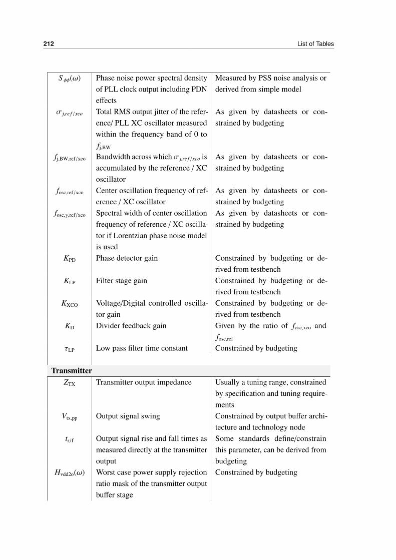
212 List of Tables
S φφ(ω) Phase noise power spectral densityof PLL clock output including PDNeffects
Measured by PSS noise analysis orderived from simple model
σ j,re f /xco Total RMS output jitter of the refer-ence/ PLL XC oscillator measuredwithin the frequency band of 0 tofj,BW
As given by datasheets or con-strained by budgeting
fj,BW,ref/xco Bandwidth across whichσ j,re f /xco isaccumulated by the reference / XCoscillator
As given by datasheets or con-strained by budgeting
fosc,ref/xco Center oscillation frequency of ref-erence / XC oscillator
As given by datasheets or con-strained by budgeting
fosc,γ,ref/xco Spectral width of center oscillationfrequency of reference / XC oscilla-tor if Lorentzian phase noise modelis used
As given by datasheets or con-strained by budgeting
KPD Phase detector gain Constrained by budgeting or de-rived from testbench
KLP Filter stage gain Constrained by budgeting or de-rived from testbench
KXCO Voltage/Digital controlled oscilla-tor gain
Constrained by budgeting or de-rived from testbench
KD Divider feedback gain Given by the ratio of fosc,xco andfosc,ref
τLP Low pass filter time constant Constrained by budgeting
TransmitterZTX Transmitter output impedance Usually a tuning range, constrained
by specification and tuning require-ments
Vtx,pp Output signal swing Constrained by output buffer archi-tecture and technology node
tr/f Output signal rise and fall times asmeasured directly at the transmitteroutput
Some standards define/constrainthis parameter, can be derived frombudgeting
Hvdd2o(ω) Worst case power supply rejectionratio mask of the transmitter outputbuffer stage
Constrained by budgeting
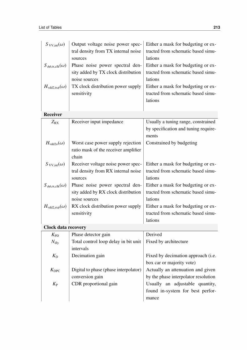
List of Tables 213
S VV,int(ω) Output voltage noise power spec-tral density from TX internal noisesources
Either a mask for budgeting or ex-tracted from schematic based simu-lations
S φφ,tx,clk(ω) Phase noise power spectral den-sity added by TX clock distributionnoise sources
Either a mask for budgeting or ex-tracted from schematic based simu-lations
Hvdd2,txφ(ω) TX clock distribution power supplysensitivity
Either a mask for budgeting or ex-tracted from schematic based simu-lations
ReceiverZRX Receiver input impedance Usually a tuning range, constrained
by specification and tuning require-ments
Hvdd2o(ω) Worst case power supply rejectionratio mask of the receiver amplifierchain
Constrained by budgeting
S VV,int(ω) Receiver voltage noise power spec-tral density from RX internal noisesources
Either a mask for budgeting or ex-tracted from schematic based simu-lations
S φφ,rx,clk(ω) Phase noise power spectral den-sity added by RX clock distributionnoise sources
Either a mask for budgeting or ex-tracted from schematic based simu-lations
Hvdd2,rxφ(ω) RX clock distribution power supplysensitivity
Either a mask for budgeting or ex-tracted from schematic based simu-lations
Clock data recoveryKPD Phase detector gain DerivedNdly Total control loop delay in bit unit
intervalsFixed by architecture
KD Decimation gain Fixed by decimation approach (i.e.box car or majority vote)
KDPC Digital to phase (phase interpolator)conversion gain
Actually an attenuation and givenby the phase interpolator resolution
KP CDR proportional gain Usually an adjustable quantity,found in-system for best perfor-mance

214 List of Tables
KI CDR integral gain Usually an adjustable quantity,found in-system for best perfor-mance
Peak Distortion Algorithmvrpda,thr Relative magnitude of an SBR tap
compared to its maximum value tostill be considered for PDA analysis
Fixed by accuracy requirements
vrpdavres PDA analysis SBR voltage resolu-tion
Fixed by accuracy requirements
Table .1: OCM link budgeting variables as defined and used throughout this text

Appendix B - Design budgeting constraints
Symbol Value Notes
Overall systemBER 10−13 Slight overconstraint to the usual
10−12 for marginUI In variationTenv 300K Room temperatured fφ 100 kHz
PLL Power distribution networkσvn,pdn 5 mVω3db,pdn 2 GHz High frequency cutoff due to on-die
capacitance of low ESR
TX/RX Power distribution networkσvn,pdn 5 mVω3db,pdn 1 GHz
Low jitter phase locked loop modelσ j,re f 750 fsfj,BW,ref 1 MHzfosc,ref 100 MHz
fosc,γ,ref 250 kHzσ j,re f 500 fsfj,BW,ref 10 MHzfosc,ref 5 GHz
fosc,γ,ref 250 kHzKPD 500KLP 1
KXCO 10 GHz/VKD 50τLP 20 ns
215

216 List of Tables
TransmitterZTX 50Ω single ended, 100Ω differen-
tialVtx,pp 800 mV differential with transmit-
ter terminated with matched loadtr/f 20 ps pre ESD compensation
Hvdd2o(ω) Simple first order high pass modelwith onset frequency of 500 MHzminimal susceptibiliy of 10−3 andmaximum of 10−2
S VV,int(ω) Simple low pass noise model with1.5 mVrms within a band of 17 GHz
S φφ,tx,clk(ω) as reported by PLL modelHvdd2,txφ(ω) - unused
ReceiverZRX 50Ω single ended, 100Ω differen-
tialHvdd2o(ω) Simple first order high pass model
with onset frequency of 500 MHzminimal susceptibiliy of 10−4 andmaximum of 10−2
CML amplifier stages with betternoise rejection than SST segmentsof transmitter at low frequencies
S VV,int(ω) Simple low pass noise model with2 mVrms within a band of 17 GHz
S φφ,rx,clk(ω) As reported by PLLHvdd2,rxφ(ω) - unusedClock data recovery
Ndly 32 Given by architecture, CDR run-ning in clk8 domain
KD 8 Simple majority votingKDPC
126 Given by PI resolution
KP128 not optimized in simulation
KI1
219 not optimized in simulation
Peak Distortion Algorithmvrpda,thr not used but fixed to 4 precursors
and 20 postcursors

List of Tables 217
vrpdavres 2.5 mV
Table .2: OCM link budgeting variable values for budgeting runs as presented in chapter 6

Bibliography
[1] Accellera. ‘SystemVerilog 3.1a Language Reference Manual’. In: (2004), p. 586. url: http:
//www.eda.org/sv/SystemVerilog%7B%5C_%7D3.1a.pdf.
[2] Accellera. Verilog-AMS Language Reference Manual v2.4. 2014. url: http : / / www .
accellera.org/downloads/standards/v-ams.
[3] David E. Bockelman and William R. Eisenstadt. ‘Combined differential and common-mode
scattering parameters: theory and simulation’. In: IEEE Transactions on Microwave Theory
and Techniques 43.7 pt 1 (1995), pp. 1530–1539. issn: 00189480. doi: 10.1109/22.392911.
arXiv: 95 [0018-9480].
[4] Bulzacchelli. ‘A 10-Gb/s 5-Tap DFE/4-Tap FFE Transceiver in 90-nm CMOS Technology’.
In: IEEE Journal of Solid-State Circuits 41.12 (Dec. 2006), pp. 2885–2900. issn: 0018-9200.
doi: 10.1109/JSSC.2006.884342. url: http://ieeexplore.ieee.org/lpdocs/
epic03/wrapper.htm?arnumber=4014602.
[5] Anthony Chan Carusone. ‘An equalizer adaptation algorithm to reduce jitter in binary
receivers’. In: IEEE Transactions on Circuits and Systems II: Express Briefs 53.9 (2006),
pp. 807–811. issn: 10577130. doi: 10.1109/TCSII.2006.881161.
[6] B.K. Casper, M. Haycock, and R. Mooney. ‘An accurate and efficient analysis method for
multi-Gb/s chip-to-chip signaling schemes’. In: 2002 Symposium on VLSI Circuits. Digest
of Technical Papers (Cat. No.02CH37302) (2002), pp. 54–57. doi: 10.1109/VLSIC.2002.
1015043.
[7] Santanu Chaudhuri et al. ‘Jitter Amplification Characterization of Passive Clock Channels
at 6.4 and 9.6 Gb/s’. In: IEEE Electrical Performance of Electronic Packaging (2006),
pp. 35–38.
[8] J Chen. Mixed-Signal Methodology Guide. 2014, p. 408. isbn: 9781300035206.
[9] James Chen. ‘Self-calibrating on-chip interconnects [Dissertation]’. PhD thesis. Stanford
University, 2012.
[10] Norbert Fliege and Markus Gaida. Signale und Systeme: Grundlagen und Anwendungen mit
MATLAB. 1st ed. Schlembach, 2008, p. 355. isbn: 978-3935340427.
219
220 Bibliography
[11] Gautam R. Gangasani et al. ‘A 16-Gb/s Backplane Transceiver With 12-Tap Current Integrat-
ing DFE and Dynamic Adaptation of Voltage Offset and Timing Drifts in 45-nm SOI CMOS
Technology’. In: IEEE Journal of Solid-State Circuits 47.8 (Aug. 2012), pp. 1828–1841. issn:
0018-9200. doi: 10.1109/JSSC.2012.2196313. url: http://ieeexplore.ieee.org/
xpls/abs%7B%5C_%7Dall.jsp?arnumber=6244847%20http://ieeexplore.ieee.
org/document/6244847/.
[12] GNU. Octave Scientific Programming Language. 2017. url: https://www.gnu.org/
software/octave/.
[13] Karthik Gopalakrishnan et al. ‘3.4 A 40/50/100Gb/s PAM-4 Ethernet transceiver in 28nm
CMOS’. In: Digest of Technical Papers - IEEE International Solid-State Circuits Conference
59 (2016), pp. 62–63. issn: 01936530. doi: 10.1109/ISSCC.2016.7417907.
[14] PCI-SIG Group. PCI Express Base Specification Revision 3.1a. 2015.
[15] Amr Amin Hafez, Ming-Shuan Chen, and Chih-Kong Ken Yang. ‘A 32-to-48Gb/s serializing
transmitter using multiphase sampling in 65nm CMOS’. In: IEEE, 2013, pp. 38–39. url:
http : / / ieeexplore . ieee . org / xpls / abs % 7B % 5C _ %7Dall . jsp ? arnumber =
6487627.
[16] H. Hatamkhani et al. ‘Power-centric design of high-speed I/Os’. In: 2006 43rd ACM/IEEE
Design Automation Conference 1 (2006), pp. 867–872. issn: 0738-100X. doi: 10.1109/DAC.
2006.229252. url: http://ieeexplore.ieee.org/lpdocs/epic03/wrapper.htm?
arnumber=1688919.
[17] IEEE. IEEE Standard for Ethernet, IEEE Standard 802.3-2015. 2015.
[18] IEEE. IEEE Standard for SystemVerilog – Unified Hardware Design, Specification and
Verification Language, IEEE Standard 1800-2012. 2012.
[19] IEEE Computer Society. IEEE Standard Verilog Hardware Description Language. 2001,
p. 791.
[20] Intel. Intel Xeon Phi Processors. 2017. url: http://www.intel.com/content/www/
us/en/products/processors/xeon-phi/xeon-phi-processors.html (visited on
02/28/2017).
[21] ITRS. International Technology Roadmap Service Report 2013. Tech. rep. 2013. url: http:
//www.itrs2.net/.
[22] M. Jeeradit et al. ‘Characterizing sampling aperture of clocked comparators’. In: IEEE
Symposium on VLSI Circuits, Digest of Technical Papers (2008), pp. 64–65. issn: 1424418046.
doi: 10.1109/VLSIC.2008.4585955.
[23] Jhih-Yu Jiang et al. ‘100Gb/s ethernet chipsets in 65nm CMOS technology’. In: IEEE, 2013,
pp. 120–121. url: http://ieeexplore.ieee.org/xpls/abs%7B%5C_%7Dall.jsp?
arnumber=6487663.
Bibliography 221
[24] Howard Johnson and Martin Graham. High-Speed Signal Propagation. 1st ed. Upper Saddle
River, NJ 07458: Prentice Hall, 2003. isbn: 0-13-084408-X.
[25] Kambiz Kaviani et al. ‘A 0.4-mW/Gb/s near-ground receiver front-end with replica transcon-
ductance termination calibration for a 16-Gb/s source-series terminated transceiver’. In:
IEEE Journal of Solid-State Circuits 48.3 (2013), pp. 636–648. issn: 00189200. doi: 10.
1109/JSSC.2013.2242714.
[26] Kambiz Kaviani et al. ‘A Tri-modal 20-Gbps/link differential/DDR3/GDDR5 memory
interface’. In: IEEE Journal of Solid-State Circuits. Vol. 47. 4. 2012, pp. 926–937. isbn:
978-4-86348-166-4. doi: 10.1109/JSSC.2012.2185370.
[27] Jaeha Kim, Brian S. Leibowitz, and Metha Jeeradit. ‘Impulse sensitivity function analysis of
periodic circuits’. In: 2008 IEEE/ACM International Conference on Computer-Aided Design
(2008), pp. 386–391. doi: 10.1109/ICCAD.2008.4681602. url: http://ieeexplore.
ieee.org/lpdocs/epic03/wrapper.htm?arnumber=4681602.
[28] Jihwan Kim et al. ‘A 16-to-40Gb/s quarter-rate NRZ/PAM4 dual-mode transmitter in 14nm
CMOS’. In: Digest of Technical Papers - IEEE International Solid-State Circuits Conference.
Vol. 58. IEEE, 2015, pp. 60–61. isbn: 9781479962235. doi: 10 . 1109 / ISSCC . 2015 .
7062925. url: http://ieeexplore.ieee.org/xpls/abs%7B%5C_%7Dall.jsp?
arnumber=7062925.
[29] Peter Kogge et al. ‘ExaScale Computing Study : Technology Challenges in Achieving
Exascale Systems’. In: Government PROcurement TR-2008-13 (2008), p. 278. doi: 10.1.1.
165.6676.
[30] Stefan Kosnac. ‘Design-Aspects of a Decision Feedback Equalizer in a 28nm Technology
[Master Thesis]’. PhD thesis. University of Heidelberg, 2016, p. 68.
[31] Kenneth S. Kundert. ‘Verification of Bit-Error Rate in Bang-Bang Clock and Data Recovery
Circuits’. In: (2010), pp. 1–22.
[32] Jri Lee, Ming-shuan Chen, and Huai-de Wang. ‘Design and Comparison of Three 20-Gb/s
Backplane Transceivers for Duobinary, PAM4 and NRZ Data’. In: 43.9 (2008), pp. 2120–
2133.
[33] Chris Madden. ‘Jitter modeling in statistical link simulation’. In: 2008 IEEE International
Symposium on Electromagnetic Compatibility 4 (2008), pp. 1–4. doi: 10.1109/ISEMC.
2008.4652155. url: http://ieeexplore.ieee.org/lpdocs/epic03/wrapper.
htm?arnumber=4652155.
[34] M. Mansuri and Chih-Kong Ken. ‘Jitter optimization based on phase-locked loop design
parameters’. en. In: IEEE Journal of Solid-State Circuits 37.11 (Nov. 2002), pp. 1375–1382.
issn: 0018-9200. doi: 10.1109/JSSC.2002.803935. url: http://ieeexplore.ieee.
org/lpdocs/epic03/wrapper.htm?arnumber=1046079.
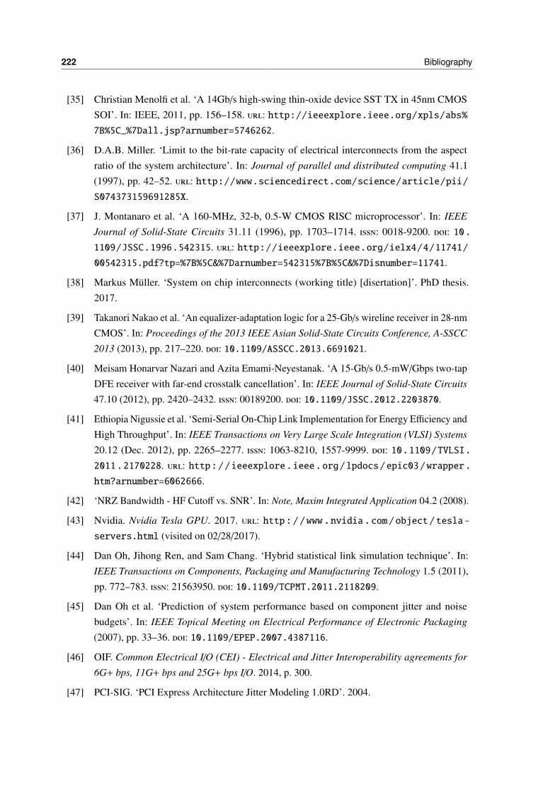
222 Bibliography
[35] Christian Menolfi et al. ‘A 14Gb/s high-swing thin-oxide device SST TX in 45nm CMOS
SOI’. In: IEEE, 2011, pp. 156–158. url: http://ieeexplore.ieee.org/xpls/abs%
7B%5C_%7Dall.jsp?arnumber=5746262.
[36] D.A.B. Miller. ‘Limit to the bit-rate capacity of electrical interconnects from the aspect
ratio of the system architecture’. In: Journal of parallel and distributed computing 41.1
(1997), pp. 42–52. url: http://www.sciencedirect.com/science/article/pii/
S074373159691285X.
[37] J. Montanaro et al. ‘A 160-MHz, 32-b, 0.5-W CMOS RISC microprocessor’. In: IEEE
Journal of Solid-State Circuits 31.11 (1996), pp. 1703–1714. issn: 0018-9200. doi: 10.
1109/JSSC.1996.542315. url: http://ieeexplore.ieee.org/ielx4/4/11741/
00542315.pdf?tp=%7B%5C&%7Darnumber=542315%7B%5C&%7Disnumber=11741.
[38] Markus Müller. ‘System on chip interconnects (working title) [disertation]’. PhD thesis.
2017.
[39] Takanori Nakao et al. ‘An equalizer-adaptation logic for a 25-Gb/s wireline receiver in 28-nm
CMOS’. In: Proceedings of the 2013 IEEE Asian Solid-State Circuits Conference, A-SSCC
2013 (2013), pp. 217–220. doi: 10.1109/ASSCC.2013.6691021.
[40] Meisam Honarvar Nazari and Azita Emami-Neyestanak. ‘A 15-Gb/s 0.5-mW/Gbps two-tap
DFE receiver with far-end crosstalk cancellation’. In: IEEE Journal of Solid-State Circuits
47.10 (2012), pp. 2420–2432. issn: 00189200. doi: 10.1109/JSSC.2012.2203870.
[41] Ethiopia Nigussie et al. ‘Semi-Serial On-Chip Link Implementation for Energy Efficiency and
High Throughput’. In: IEEE Transactions on Very Large Scale Integration (VLSI) Systems
20.12 (Dec. 2012), pp. 2265–2277. issn: 1063-8210, 1557-9999. doi: 10.1109/TVLSI.
2011.2170228. url: http://ieeexplore.ieee.org/lpdocs/epic03/wrapper.
htm?arnumber=6062666.
[42] ‘NRZ Bandwidth - HF Cutoff vs. SNR’. In: Note, Maxim Integrated Application 04.2 (2008).
[43] Nvidia. Nvidia Tesla GPU. 2017. url: http://www.nvidia.com/object/tesla-
servers.html (visited on 02/28/2017).
[44] Dan Oh, Jihong Ren, and Sam Chang. ‘Hybrid statistical link simulation technique’. In:
IEEE Transactions on Components, Packaging and Manufacturing Technology 1.5 (2011),
pp. 772–783. issn: 21563950. doi: 10.1109/TCPMT.2011.2118209.
[45] Dan Oh et al. ‘Prediction of system performance based on component jitter and noise
budgets’. In: IEEE Topical Meeting on Electrical Performance of Electronic Packaging
(2007), pp. 33–36. doi: 10.1109/EPEP.2007.4387116.
[46] OIF. Common Electrical I/O (CEI) - Electrical and Jitter Interoperability agreements for
6G+ bps, 11G+ bps and 25G+ bps I/O. 2014, p. 300.
[47] PCI-SIG. ‘PCI Express Architecture Jitter Modeling 1.0RD’. 2004.
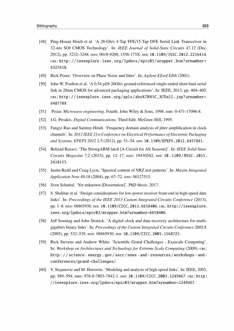
Bibliography 223
[48] Ping-Hsuan Hsieh et al. ‘A 28-Gb/s 4-Tap FFE/15-Tap DFE Serial Link Transceiver in
32-nm SOI CMOS Technology’. In: IEEE Journal of Solid-State Circuits 47.12 (Dec.
2012), pp. 3232–3248. issn: 0018-9200, 1558-173X. doi: 10.1109/JSSC.2012.2216414.
url: http://ieeexplore.ieee.org/lpdocs/epic03/wrapper.htm?arnumber=
6327618.
[49] Rick Poore. ‘Overview on Phase Noise and Jitter’. In: Agilent EEsof EDA (2001).
[50] John W. Poulton et al. ‘A 0.54 pJ/b 20Gb/s ground-referenced single-ended short-haul serial
link in 28nm CMOS for advanced packaging applications’. In: IEEE, 2013, pp. 404–405.
url: http://ieeexplore.ieee.org/xpls/abs%7B%5C_%7Dall.jsp?arnumber=
6487789.
[51] Pozar. Microwave engineering. Fourth. John Wiley & Sons, 1998. isbn: 0-471-17096-8.
[52] J.G. Proakis. Digital Communications. Third Edit. McGraw-Hill, 1995.
[53] Fangyi Rao and Sammy Hindi. ‘Frequency domain analysis of jitter amplification in clock
channels’. In: 2012 IEEE 21st Conference on Electrical Performance of Electronic Packaging
and Systems, EPEPS 2012 2.5 (2012), pp. 51–54. doi: 10.1109/EPEPS.2012.6457841.
[54] Behzad Razavi. ‘The StrongARM latch [A Circuit for All Seasons]’. In: IEEE Solid-State
Circuits Magazine 7.2 (2015), pp. 12–17. issn: 19430582. doi: 10.1109/MSSC.2015.
2418155.
[55] Justin Redd and Craig Lyon. ‘Spectral content of NRZ test patterns’. In: Maxim Integrated
Application Note 49.18 (2004), pp. 67–72. issn: 00127515.
[56] Sven Schatral. ‘Yet unknown [Dissertation]’. PhD thesis. 2017.
[57] S. Shekhar et al. ‘Design considerations for low-power receiver front-end in high-speed data
links’. In: Proceedings of the IEEE 2013 Custom Integrated Circuits Conference (2013),
pp. 1–8. issn: 08865930. doi: 10.1109/CICC.2013.6658406. url: http://ieeexplore.
ieee.org/lpdocs/epic03/wrapper.htm?arnumber=6658406.
[58] Jeff Sonntag and John Stonick. ‘A digital clock and data recovery architecture for multi-
gigabit/s binary links’. In: Proceedings of the Custom Integrated Circuits Conference 2005.8
(2005), pp. 532–539. issn: 08865930. doi: 10.1109/CICC.2005.1568725.
[59] Rick Stevens and Andrew White. ‘Scientific Grand Challenges - Exascale Computing’.
In: Workshop on Architectures and Technology for Extreme Scale Computing (2009). url:
http://science.energy.gov/ascr/news-and-resources/workshops-and-
conferences/grand-challenges/.
[60] V. Stojanovic and M. Horowitz. ‘Modeling and analysis of high-speed links’. In: IEEE, 2003,
pp. 589–594. isbn: 978-0-7803-7842-1. doi: 10.1109/CICC.2003.1249467. url: http:
//ieeexplore.ieee.org/lpdocs/epic03/wrapper.htm?arnumber=1249467.
224 Bibliography
[61] Vladimir Stojanovic, Amir Amirkhany, and Mark A. Horowitz. ‘Optimal linear precoding
with theoretical and practical data rates in high-speed serial-link backplane communication’.
In: vol. 5. IEEE, 2004, pp. 2799–2806. url: http://ieeexplore.ieee.org/xpls/abs%
7B%5C_%7Dall.jsp?arnumber=1313040.
[62] T. Toifl et al. ‘A 22-Gb/s PAM-4 Receiver in 90-nm CMOS SOI Technology’. en. In:
IEEE Journal of Solid-State Circuits 41.4 (Apr. 2006), pp. 954–965. issn: 0018-9200. doi:
10.1109/JSSC.2006.870898. url: http://ieeexplore.ieee.org/lpdocs/epic03/
wrapper.htm?arnumber=1610640.
[63] M Tsuk et al. ‘An electrical-level superposed-edge approach to statistical serial link sim-
ulation’. In: Computer-Aided Design - Digest of Technical Papers, 2009. ICCAD 2009.
IEEE/ACM International Conference on (2009), pp. 717–724. issn: 1092-3152. doi: 10.
1145/1687399.1687533.
[64] A X Widmer and P A Franaszek. ‘A DC-Balanced, Partitioned-Block, 8B/10B Transmission
Code’. In: IBM Journal of Research and Development 27.5 (1983), pp. 440–451. issn:
0018-8646. doi: 10.1147/rd.275.0440.
[65] Ricki Dee Williams and Theresa Sze. ‘JEDEC Server Memory Roadmap’. In: 2012.
[66] Hyosup Won et al. ‘An on-chip stochastic sigma-tracking eye-opening monitor for BER-
optimal adaptive equalization’. In: Proceedings of the Custom Integrated Circuits Conference
2015-Novem (2015), pp. 15–18. issn: 08865930. doi: 10.1109/CICC.2015.7338374.
[67] Arash Zargaran-yazd and Wendemagagnehu T Beyene. ‘Discrete-Time Modeling and Simu-
lation Considerations for High-Speed Serial Links’. In: (2014), pp. 165–168.


![Resenha: BENVINDO, JULIANO ZAIDEN (2010). [OS LIMITES DA JURISDIÇÃO CONSTITUCIONAL: DESCONSTRUINDO O BALANCEAMENTO E O ATIVISMO JUDICIAL]. HEIDELBERG: SPRINGER.](https://static.fdokumen.com/doc/165x107/63442faaf474639c9b044216/resenha-benvindo-juliano-zaiden-2010-os-limites-da-jurisdicao-constitucional.jpg)