
Digital Signal Processing System Design: LabVIEW-Based ...
342
-
Upload
khangminh22 -
Category
Documents
-
view
0 -
download
0
Transcript of Digital Signal Processing System Design: LabVIEW-Based ...


Digital Signal Processing System
Design: LabVIEW-Based Hybrid
Programming
Nasser Kehtarnavaz

This page intentionally left blank

Digital Signal Processing System
Design: LabVIEW-Based Hybrid
Programming
by Nasser Kehtarnavaz
University of Texas at Dallas
With laboratory contributions by Namjin Kim
and Qingzhong Peng
Amsterdam • Boston • Heidelberg • London • New York • Oxford Paris • San Diego • San Francisco • Singapore • Sydney • Tokyo
Academic Press is an imprint of Elsevier

Academic Press is an imprint of Elsevier30 Corporate Drive, Suite 400, Burlington, MA 01803, USA525 B Street, Suite 1900, San Diego, California 92101-4495, USA84 Theobald’s Road, London WC1X 8RR, UK
Copyright # 2008, Elsevier Inc. All rights reserved.
Cover image: supplied by authorCover Design: Alisa AndreolaCover Direction: Alisa Andreola
No part of this publication may be reproduced or transmitted in any form or by any means, electronicor mechanical, including photocopy, recording, or any information storage and retrieval system,without permission in writing from the publisher.
Permissions may be sought directly from Elsevier’s Science & Technology Rights Department inOxford, UK: phone: (þ44) 1865 843830, fax: (þ44) 1865 853333, E-mail: [email protected] may also complete your request online via the Elsevier homepage (http://elsevier.com), byselecting “Support & Contact” then “Copyright and Permission” and then “Obtaining Permissions.”
Library of Congress Cataloging-in-Publication DataApplication Submitted
British Library Cataloguing-in-Publication DataA catalogue record for this book is available from the British Library.
ISBN: 978-0-12-374490-6
For information on all Academic Press publicationsvisit our Web site at www.books.elsevier.com
Printed in the United States of America08 09 10 9 8 7 6 5 4 3 2 1

Contents
Preface.............................................................................................. xi
What’s On the CD-ROM? .................................................................. xiii
Chapter 1: Introduction ..................................................................... 1
1.1 Digital Signal Processing Hands-On Lab Courses ......................................................21.2 Organization ..................................................................................................................31.3 Software Installation.....................................................................................................31.4 Updates..........................................................................................................................41.5 Bibliography ..................................................................................................................4
Chapter 2: LabVIEW Graphical Programming Environment ............... 5
2.1 Virtual Instruments (VIs) .............................................................................................52.1.1 Front Panel and Block Diagram......................................................................... 52.1.2 Icon and Connector Pane .................................................................................. 6
2.2 Graphical Environment ................................................................................................72.2.1 Functions Palette ................................................................................................ 72.2.2 Controls Palette .................................................................................................. 82.2.3 Tools Palette ....................................................................................................... 8
2.3 Building a Front Panel..................................................................................................92.3.1 Controls ............................................................................................................... 92.3.2 Indicators ........................................................................................................... 102.3.3 Align, Distribute, and Resize Objects.............................................................. 10
2.4 Building a Block Diagram ..........................................................................................112.4.1 Express VI and Function .................................................................................. 112.4.2 Terminal Icons .................................................................................................. 122.4.3 Wires.................................................................................................................. 122.4.4 Structures........................................................................................................... 13
2.4.4.1 For Loop.................................................................................................132.4.4.2 While Loop............................................................................................142.4.4.3 Case Structure .......................................................................................14
v

2.5 MathScript...................................................................................................................142.6 Grouping Data: Array & Cluster ...............................................................................162.7 Debugging and Profiling VIs.......................................................................................16
2.7.1 Probe Tool......................................................................................................... 162.7.2 Profile Tool........................................................................................................ 16
2.8 Bibliography ................................................................................................................18
Lab 1: Getting Familiar with LabVIEW: Part I ................................... 19
L1.1 Building a Simple VI................................................................................................20L1.1.1 VI Creation................................................................................................... 20L1.1.2 SubVI Creation............................................................................................. 25
L1.2 Using Structures and SubVIs ...................................................................................29L1.3 Create an Array with Indexing................................................................................33L1.4 Debugging VIs: Probe Tool ......................................................................................34L1.5 Bibliography ..............................................................................................................36L1.6 Lab Experiments .......................................................................................................36
Lab 2: Getting Familiar with LabVIEW: Part II .................................. 37
L2.1 Express VIs Versus Regular VIs ...............................................................................37L2.1.1 Building a System VI with Express VIs....................................................... 37L2.1.2 Building a System with Regular VIs............................................................ 45
L2.2 Hybrid Programming ................................................................................................50L2.2.1 MathScript Feature....................................................................................... 50L2.2.2 Call Library Function Feature...................................................................... 51
L2.2.2.1 Building C DLL Using MS Visual Studio .................................... 51L2.2.2.2 Calling C DLL from LabVIEW..................................................... 52
L2.3 Profile VI ...................................................................................................................54L2.4 Bibliography ..............................................................................................................56L2.5 Lab Experiments .......................................................................................................56
Chapter 3: Analog-to-Digital Signal Conversion............................... 57
3.1 Sampling......................................................................................................................573.1.1 Fast Fourier Transform...................................................................................... 60
3.2 Quantization................................................................................................................623.3 Signal Reconstruction.................................................................................................653.4 Bibliography ................................................................................................................67
Lab 3: Sampling, Quantization, and Reconstruction ........................ 69
L3.1 Aliasing .....................................................................................................................69L3.2 Fast Fourier Transform .............................................................................................76L3.3 Quantization..............................................................................................................80L3.4 Signal Reconstruction ..............................................................................................87L3.5 Bibliography ..............................................................................................................90L3.6 Lab Experiments .......................................................................................................91
vi
Contents

Chapter 4: Digital Filtering .............................................................. 93
4.1 Digital Filtering...........................................................................................................934.1.1 Difference Equations ......................................................................................... 934.1.2 Stability and Structure...................................................................................... 95
4.2 LabVIEW Digital Filter Design Toolkit ....................................................................974.2.1 Filter Design ...................................................................................................... 974.2.2 Analysis of Filter Design .................................................................................. 984.2.3 Fixed-Point Filter Design.................................................................................. 984.2.4 Multi-rate Digital Filter Design........................................................................ 98
4.3 Bibliography ................................................................................................................98
Lab 4: FIR/IIR Filtering System Design............................................. 99
L4.1 FIR Filtering System.................................................................................................99L4.1.1 Design FIR Filter with DFD Toolkit ........................................................... 99L4.1.2 Creating a Filtering System VI.................................................................. 101
L4.2 IIR Filtering System................................................................................................106L4.2.1 IIR Filter Design ......................................................................................... 106L4.2.2 Filtering System .......................................................................................... 110
L4.3 Building Filtering System Using Filter Coefficients .............................................112L4.4 Filter Design Without Using DFD Toolkit ...........................................................113L4.5 Building Filtering System Using Dynamic Link Library (DLL)...........................115
L4.5.1 Point-by-Point Processing .......................................................................... 115L4.5.2 Creating DLL in C ..................................................................................... 118L4.5.3 Calling DLL from LabVIEW ..................................................................... 119
L4.6 Bibliography ............................................................................................................120L4.7 Lab Experiments .....................................................................................................121
Chapter 5: Fixed-Point versus Floating-Point.................................. 123
5.1 Q-format Number Representation ...........................................................................1235.2 Finite Word Length Effects ......................................................................................1275.3 Floating-Point Number Representation...................................................................1285.4 Overflow and Scaling................................................................................................1305.5 Data Types in LabVIEW..........................................................................................1305.6 Bibliography ..............................................................................................................132
Lab 5: Data Type and Scaling ........................................................ 133
L5.1 Handling Data Types in LabVIEW .......................................................................133L5.2 Overflow Handling .................................................................................................135
L5.2.1 Q-Format Conversion................................................................................. 137L5.2.2 Creating a Polymorphic VI........................................................................ 138
vii
Contents

L5.3 Scaling Approach ...................................................................................................140L5.4 Digital Filtering in Fixed-Point Format.................................................................143
L5.4.1 Design and Analysis of Fixed-Point Digital Filtering System.................. 143L5.4.2 Filtering System .......................................................................................... 146L5.4.3 Fixed-Point IIR Filter Example.................................................................. 150
L5.5 Bibliography ............................................................................................................154L5.6 Lab Experiments .....................................................................................................154
Chapter 6: Adaptive Filtering......................................................... 157
6.1 System Identification ................................................................................................1576.2 Noise Cancellation ...................................................................................................1586.3 Bibliography ..............................................................................................................160
Lab 6: Adaptive Filtering Systems.................................................. 161
L6.1 System Identification ..............................................................................................161L6.1.1 Least Mean Square (LMS) Algorithm ...................................................... 161L6.1.2 Waveform Chart......................................................................................... 163L6.1.3 Shift Register and Feedback Node ............................................................ 163
L6.2 Noise Cancellation .................................................................................................168L6.3 Lab Experiments .....................................................................................................173
Chapter 7: Frequency Domain Processing...................................... 175
7.1 Discrete Fourier Transform (DFT) and Fast Fourier Transform (FFT) .................1757.2 Short-Time Fourier Transform (STFT) ...................................................................1767.3 Discrete Wavelet Transform (DWT) ......................................................................1787.4 Signal Processing Toolset .........................................................................................1807.5 Bibliography ..............................................................................................................181
Lab 7: FFT, STFT, and DWT............................................................ 183
L7.1 FFT Versus STFT ...................................................................................................183L7.1.1 Property Node............................................................................................. 189
L7.2 DWT .......................................................................................................................190L7.3 Bibliography ............................................................................................................195L7.4 Lab Experiments .....................................................................................................195
Chapter 8: DSP Implementation Platform: TMS320C6xArchitecture and Software Tools .............................................. 197
8.1 TMS320C6X DSP.....................................................................................................1978.1.1 Pipelined CPU ................................................................................................ 1988.1.2 C64x DSP........................................................................................................ 199
viii
Contents

8.2 C6x DSK Target Boards ...........................................................................................2018.2.1 Board Configuration and Peripherals ............................................................. 2018.2.2 Memory Organization ..................................................................................... 202
8.3 DSP Programming.....................................................................................................2038.3.1 Software Tools: Code Composer Studio........................................................ 2048.3.2 Linking............................................................................................................. 2058.3.3 Compiling........................................................................................................ 205
8.4 Bibliography ..............................................................................................................206
Lab 8: Getting Familiar with Code Composer Studio ...................... 207
L8.1 Code Composer Studio...........................................................................................207L8.2 Creating Projects ....................................................................................................207L8.3 Debugging Tools .....................................................................................................214L8.4 Bibliography ............................................................................................................222
Chapter 9: LabVIEW DSP Integration ............................................. 223
9.1 Communication with LabVIEW: Real-Time Data Exchange (RTDX).................2239.2 LabVIEW DSP Test Integration Toolkit for TI DSP.............................................2239.3 Combined Implementation: Gain Example.............................................................224
9.3.1 LabVIEW Configuration................................................................................. 2269.3.2 DSP Configuration.......................................................................................... 227
9.4 Bibliography ..............................................................................................................230
Lab 9: DSP Integration Examples ................................................... 231
L9.1 CCS Automation....................................................................................................231L9.2 Digital Filtering.......................................................................................................233
L9.2.1 FIR Filter..................................................................................................... 233L9.2.2 IIR Filter ..................................................................................................... 238
L9.3 Fixed-Point Implementation ..................................................................................244L9.4 Adaptive Filtering Systems ....................................................................................248
L9.4.1 System Identification.................................................................................. 248L9.4.2 Noise Cancellation..................................................................................... 252
L9.5 Frequency Processing: FFT .....................................................................................254L9.6 Bibliography ............................................................................................................264
Chapter 10: DSP System Design: Dual Tone Multi-Frequency(DTMF) Signaling....................................................................... 265
10.1 Bibliography ............................................................................................................268
Lab 10: Hybrid Programming of Dual Tone Multi-FrequencySystem....................................................................................... 269
L10.1 DTMF Tone Generator System...........................................................................269L10.2 DTMF Decoder System ........................................................................................273L10.3 Bibliography ..........................................................................................................275
ix
Contents
Chapter 11: DSP System Design: Software-Defined Radio .............. 277
11.1 QAM Transmitter...................................................................................................27711.2 QAM Receiver........................................................................................................280
11.2.1 Ideal QAM Demodulation.......................................................................... 28011.2.2 Frame Synchronization................................................................................ 28111.2.3 Decision-Based Carrier Tracking................................................................ 281
11.3 Bibliography ............................................................................................................284
Lab 11: Hybrid Programming of a 4-QAM Modem System.............. 285
L11.1 QAM Transmitter ................................................................................................286L11.2 QAM Receiver......................................................................................................289L11.3 Bibliography ..........................................................................................................301
Chapter 12: DSP System Design: Cochlear Implant Simulator........ 303
12.1 Cochlear Implant System .......................................................................................30312.2 Real-Time Implementation ....................................................................................305
12.2.1 Pre-Emphasis Filter...................................................................................... 30612.2.2 Filterbank for Decomposition and Synthesis ............................................. 30612.2.3 Envelope Detection..................................................................................... 30612.2.4 White Noise Excitation .............................................................................. 307
12.3 Bibliography ............................................................................................................308
Lab 12: Hybrid Programming of Cochlear Implant SimulatorSystem....................................................................................... 309
L12.1 Filter Design..........................................................................................................310L12.1.1 Bandpass Filter Design............................................................................ 312L12.1.2 Lowpass Filter Design ............................................................................. 314
L12.2 Real-Time Implementation..................................................................................315L12.3 Bibliography ..........................................................................................................320
Index .............................................................................................. 321
x
Contents

Preface
The previous edition of this book, titled Digital Signal Processing System-LevelDesign Using LabVIEW, showed how LabVIEWTM graphical programming can beused to build and analyze digital signal processing (DSP) systems in an interactivemanner and in relatively shorter times as compared to text-based programming.The motivation for writing the previous edition was derived from the observationthat many students taking DSP lab courses, in particular at the undergraduate level,often struggle and spend a fair amount of their time debugging C and MATLABW
codes in lab sessions instead of placing more effort into analyzing and thusunderstanding signal processing systems.
In this second edition of the book, graphical and textual programming are combinedto provide a hybrid programming approach toward achieving a more effectivemechanism to build and analyze DSP systems. Textual programming and graphicalprogramming have their own merits and demerits from a programming point of view.In general, math operations are found to be easier to code in textual mode. Forexample, MATLAB provides a rich set of built-in functions for performing signalprocessing vector and matrix-based math operations. On the other hand, graphicalprogramming offers an easy-to-build interactive and visualization environment and amore intuitive approach toward building signal processing systems.
In an effort to bring together the preferred features of textual and graphicalprogramming, the labs in the previous edition have been redesigned by incorporatingMATLAB code blocks or modules into the LabVIEW graphical programmingenvironment via its new MathScripting feature. In other words, the coding formath-oriented modules is now done using M-files, while interactivity, visualization,and modularity are maintained by using LabVIEW.
xi

In addition to the hybrid programming approach adopted in this second edition, thelabs have been redesigned based on the latest release of LabVIEW (LabVIEW 8.5) atthe time of this writing instead of LabVIEW 7.1, which was utilized in the firstedition.
I would like to express my appreciation and gratitude to National Instruments, inparticular the Academic Marketing Division, for their support of this book.
Nasser KehtarnavazDecember 2007
xii
Preface

What’s On the CD-ROM?
� The accompanying CD-ROM includes all the lab files discussed throughout the
book. These files are placed in corresponding folders as follows:
○ Lab01: Getting Familiar with LabVIEW: Part I
○ Lab02: Getting Familiar with LabVIEW: Part II
○ Lab03: Sampling, Quantization, and Reconstruction
○ Lab04: FIR/IIR Filtering System Design
○ Lab05: Data Type and Scaling
○ Lab06: Adaptive Filtering Systems
○ Lab07: FFT, STFT, and DWT
○ Lab08: Getting Familiar with Code Composer Studio
○ Lab09: DSP Integration Examples
○ Lab10: Hybrid Programming of Dual Tone Multi-Frequency System
○ Lab11: Hybrid Programming of 4-QAM Modem System
○ Lab12: Hybrid Programming of Cochlear Implant Simulator System
� To run the lab files, the National Instruments LabVIEW 8.5 is used and assumed
installed. The lab files need to be copied into the folder “C:\LabVIEW Labs\”, as
shown in the following figure.
xiii

� For Lab 8 and Lab 9, the Texas Instruments Code Composer StudioTM (CCStudio)
version 3.0 is used and assumed installed in the folder “C:\CCStudio\”. The
subfolders correspond to the following DSP platforms:
○ DSK 6416
○ DSK 6713
○ Simulator (configured as DSK6713 as shown in the following figure)
xiv
What’s On the CD-ROM?

xv
What’s On the CD-ROM?

This page intentionally left blank

CHAPTER1Introduction
The field of digital signal processing (DSP) has experienced a considerable growth inthe past two decades, primarily due to the availability and advancements in digitalsignal processors (also called DSPs). Nowadays, DSP systems such as cell phones andhigh-speed modems have become an integral part of our lives.
In general, sensors generate analog signals in response to various physical phenom-ena that occur in an analog manner (i.e., in continuous-time and amplitude). Pro-cessing of signals can be done either in analog or digital domain. To perform theprocessing of an analog signal in digital domain, it is required that a digital signal isformed by sampling and quantizing (digitizing) the analog signal. Hence, in contrastto an analog signal, a digital signal is discrete in both time and amplitude. Thedigitization process is achieved via an analog-to-digital (A/D) converter. The field ofDSP involves the manipulation of digital signals in order to modify their charac-teristics or to extract useful information from them.
There are many reasons why one wishes to process an analog signal in a digitalfashion by converting it into a digital signal. The main reason is that digital pro-cessing offers programmability, which means the same processor hardware can beused for many different applications by simply changing the code residing in mem-ory. Another reason is that digital circuits provide a more stable and tolerant outputthan analog circuits—for instance, when subjected to temperature changes. Inaddition, the advantage of operating in digital domain may be intrinsic. For example,a linear phase filter or a steep-cutoff notch filter can be easily realized by using digitalsignal processing techniques, and many adaptive systems are achievable in a practi-cal product only via digital manipulation of signals. In essence, digital representation(0’s and 1’s) allows voice, audio, image, and video data to be treated the same forerror-tolerant digital transmission and storage purposes.
1

1.1 Digital Signal Processing Hands-On Lab Courses
Nearly all electrical engineering curricula include DSP courses. DSP lab or designcourses are also being offered at many universities concurrently or as follow-ups toDSP theory courses. These hands-on lab courses have played a major role in betterunderstanding of DSP concepts. A number of textbooks, e.g. [1–5], have been writ-ten to provide the teaching materials for DSP lab courses. The programming lan-guage used in these textbooks consists of either C, MATLABW, or Assembly, whichare all text-based languages. In addition to these text-based languages, it is becomingimportant for students to gain experience in block-based or graphical (G) program-ming or environment for the purpose of designing DSP systems in a relatively shortamount of time. Graphical programming offers an interactive and a more intuitiveapproach toward building DSP systems. Thus, the main objective of this book is toprovide a block-based or system-level programming approach in DSP lab courses.The system-level programming environment chosen is LabVIEW.
Laboratory Virtual Instrumentation Engineering Workbench (LabVIEW) is agraphical programming environment developed by National Instruments (NI) whichallows performing high-level or system-level designs. It uses a graphical programminglanguage to create so-called Virtual Instrument (VI) blocks in an intuitive flowchart-like manner. A design is achieved by integrating different blocks, components, orsubsystems within a graphical framework. LabVIEW provides data acquisition,analysis, and visualization features well suited for DSP system design. It is also anopen environment accommodating MATLAB and C Dynamic Link Libraries(DLLs).
This book is written primarily for those who are already familiar with signal pro-cessing concepts and are interested in designing signal processing systems withoutneeding them to be proficient C or MATLAB programmers. After familiarizing thereader with LabVIEW, the book covers a LabVIEW-based approach to genericexperiments encountered in a typical DSP lab course. It brings together in one placethe information scattered in several NI LabVIEW manuals to provide the necessarytools and know-how for designing signal processing systems within a one-semesterlab course. This book can also be used as a self-study LabVIEW guide towarddesigning and analyzing signal processing systems.
In addition, for those interested in DSP hardware implementation, two chapters inthe book are dedicated to executing selected portions of a LabVIEW designed systemon an actual DSP processor. The DSP processor chosen is TMS320C6000. Thisprocessor has been manufactured by Texas Instruments (TI) for computationallyintensive signal processing applications. The DSP hardware utilized to interface with
2
Chapter 1

LabVIEW is the widely adopted TI’s C6416 or C6713 DSP Starter Kit (DSK) board.It should be mentioned that since the DSP hardware implementation aspect ofthe labs (which includes C programs) is independent of the LabVIEW imple-mentation, those who are not interested in the DSP hardware implementationmay skip these two chapters.
1.2 Organization
The book includes 12 chapters and 12 labs. After this introduction, the LabVIEWprogramming environment is presented in Chapter 2. Lab 1 and Lab 2 in Chapter 2provide a tutorial on getting familiar with the LabVIEW programming environ-ment. Lab 1 provides a general introduction to LabVIEW, and Lab 2 covers buildingsignal processing systems graphically. Lab 2 also shows how to incorporate M-filenodes or blocks within LabVIEW. The topic of analog-to-digital signal conversion ispresented in Chapter 3 followed by Lab 3 covering signal sampling experiments.Chapter 4 involves digital filtering. Lab 4 in Chapter 4 shows how to use LabVIEWto design FIR and IIR digital filters. In Chapter 5, fixed-point versus floating-pointimplementation issues are discussed, followed by Lab 5 covering data type andfixed-point effect experiments. In Chapter 6, the topic of adaptive filtering is dis-cussed. Lab 6 in Chapter 6 covers two adaptive filtering systems consisting of systemidentification and noise cancellation. Chapter 7 presents frequency domainprocessing, followed by Lab 7 covering the three widely used transforms in signalprocessing: fast Fourier transform (FFT), short-time Fourier transform (STFT), anddiscrete wavelet transform (DWT). Chapter 8 discusses the implementation of aLabVIEW-designed system on the TMS320C6000 DSP processor. First, an overviewof the TMS320C6000 architecture is provided. Then, in Lab 8, a tutorial ispresented to show how to use the Code Composer Studio (CCStudio) softwaredevelopment tool to achieve the DSP hardware implementation. As a continuationof Chapter 8, Chapter 9 and Lab 9 discuss the issues related to the interfacing ofLabVIEW and the DSP processor. Chapters 10 through 12 and Labs 10 through 12,respectively, discuss the following three DSP systems or project examples that aredesigned in a hybrid mode or a combination of graphical and textual modes: (i) dualtone multi-frequency (DTMF) signaling, (ii) software-defined radio, and (iii)cochlear implant simulator.
1.3 Software Installation
LabVIEW 8.5, which is the latest version at the time of this writing, can be installedby running setup.exe on the LabVIEW Core DVD. Some lab portions use the Lab-VIEW toolkits “Digital Filter Design,” “Advanced Signal Processing,” and “DSP Test
3
Introduction

Integration for TI DSP.” The toolkit “Digital Filter Design” appears under the Lab-VIEW Core DVD and can be included while installing LabVIEW 8.5. The toolkits“Advanced Signal Processing” and “DSP Test Integration for TI DSP” appear on theSignal Processing and Communications DVD and can be installed by runningsetup.exe on this DVD. To generate C DLLs, it is required to have Microsoft VisualStudioW or a similar C development environment installed. To use the MATLABscript node feature of LabVIEW, it is required to have MATLAB Version 6.0 orlater installed.
If one desires to run parts of a LabVIEW-designed system on a DSP processor, thenit is required to install the Code Composer Studio (CCStudio) software tool byrunning setup.exe on the CCStudio CD. In the DSK related labs, CCStudio v3.0 isused.
The accompanying CD includes all the files necessary for running the labs coveredthroughout the book.
1.4 Updates
Considering that any programming environment goes through enhancements andupdates, it is expected that there will be updates of LabVIEW and its toolkits. Toaccommodate for such updates and to make sure that the labs provided in the bookcan still be used in DSP lab courses, any new version of the labs will be posted at thewebsite http://www.utdallas.edu/~kehtar/LabVIEW for easy access. It is recom-mended that this website is periodically checked to download any necessary updates.
1.5 Bibliography
[1] N. Kehtarnavaz, Real-Time Digital Signal Processing Based on the TMS320C6000,Elsevier, 2005.
[2] S. Kuo and W-S. Gan, Digital Signal Processors: Architectures, Implementations,and Applications, Prentice-Hall, 2005.
[3] R. Chassaing, DSP Applications Using C and the TMS320C6x DSK, WileyInter-Science, 2002.
[4] T. Welch, C. Wright and M. Morrow, Real-Time Digital Signal Processingfrom MATLAB to C with the TMS320C6x DSK, CRC Press, 2006.
[5] L. Tan, Digital Signal Processing: Fundamentals and Applications, Elsevier, 2007.
4
Chapter 1

CHAPTER2LabVIEW Graphical Programming
Environment
LabVIEW constitutes a graphical programming environment that allows one todesign and analyze a DSP system in a shorter time as compared to text-basedprogramming environments. LabVIEW graphical programs are called VirtualInstruments (VIs). VIs run based on the concept of data flow programming. Thismeans that execution of a block or a graphical component is dependent on the flowof data, or more specifically a block executes when data are made available at allof its inputs. Output data of the block are then sent to all other connectedblocks. Data flow programming allows multiple operations to be performed inparallel, since its execution is determined by the flow of data and not bysequential lines of code.
2.1 Virtual Instruments (VIs)
A VI consists of two major components, which include a Front Panel (FP) and aBlock Diagram (BD). An FP provides the user-interface of a program, whereas a BDincorporates its graphical code. When a VI is located within the block diagram ofanother VI, it is called a subVI. LabVIEW VIs are modular, meaning that any VI orsubVI can be run by itself.
2.1.1 Front Panel and Block Diagram
An FP contains the user interfaces of a VI shown in a BD. Inputs to a VI arerepresented by controls. Knobs, pushbuttons, and dials are a few examples ofcontrols. Outputs from a VI are represented by indicators. Graphs, LEDs (lightindicators), and meters are a few examples of indicators. As a VI runs, its FP providesa display or user interface of controls (inputs) and indicators (outputs).
5

A BD contains terminal icons, nodes, wires, and structures. Terminal icons areinterfaces through which data are exchanged between an FP and a BD. Theycorrespond to controls or indicators that appear on an FP. Whenever a control orindicator is placed on an FP, a terminal icon gets added to the corresponding BD.A node represents an object which has input and/or output connectors and performsa certain function. SubVIs and functions are examples of nodes. Wires establish theflow of data in a BD. Structures are used to control the flow of a program such asrepetitions or conditional executions. Figure 2-1 shows what an FP and a BD windowlook like.
2.1.2 Icon and Connector Pane
A VI icon is a graphical representation of a VI. It appears in the top right corner of aBD or an FP window. When a VI is inserted in a BD as a subVI, its icon getsdisplayed.
A connector pane defines inputs (controls) and outputs (indicators) of a VI. Thenumber of inputs and outputs can be changed by using different connector panepatterns. In Figure 2-1, a VI icon is shown at the top right corner of the BD and itscorresponding connector pane having two inputs and one output is shown at the topright corner of the FP.
Figure 2-1: LabVIEW windows: Front Panel and Block Diagram.
6
Chapter 2

2.2 Graphical Environment
2.2.1 Functions Palette
The Functions palette, shown in Figure 2-2, provides various function VIs orblocks for building a system. This palette can be displayed by right-clicking onan open area of a BD. Note that this palette can be displayed only in a BD.
Figure 2-2: Functions palette.
7
LabVIEW Graphical Programming Environment

2.2.2 Controls Palette
The Controls palette, shown inFigure 2-3, provides controls andindicators of an FP. This palette canbe displayed by right-clicking onan open area of an FP. Note that thispalette can be displayed only in anFP.
2.2.3 Tools Palette
The Tools palette provides variousoperation modes of the mouse cursorfor building or debugging a VI. TheTools palette and the frequently usedtools are shown in Figure 2-4.
Each tool is utilized for a specific task.For example, the Wiring tool is usedto wire objects in a BD. If theautomatic tool selection mode isenabled by clicking the Automatic ToolSelection button, LabVIEW selectsthe best matching tool based on acurrent cursor position. Figure 2-3: Controls palette.
Figure 2-4: Tools palette.
8
Chapter 2

2.3 Building a Front Panel
In general, a VI is put together by going back and forth between an FP and a BD,placing inputs/outputs on the FP and building blocks on the BD.
2.3.1 Controls
Controls make up the inputs to a VI. Controls grouped in the Numeric Controls palette(Controls » Express » Num Ctrls) are used for numerical inputs, grouped in the Buttons &Switches palette (Controls » Express » Buttons) for Boolean inputs, and grouped in the TextControls palette (Controls » Express » Text Ctrls) for text and enumeration inputs.These control options are displayed in Figure 2-5.
Figure 2-5: Control palettes.
9
LabVIEW Graphical Programming Environment

2.3.2 Indicators
Indicators make up the outputs of a VI. Indicators grouped in the Numeric Indicatorspalette (Controls » Express » Num Inds) are used for numerical outputs, grouped in theLEDs palette (Controls » Express » LEDs) for Boolean outputs, grouped in the TextIndicators palette (Controls » Express » Text Inds) for text outputs, and grouped in theGraph Indicators palette (Controls » Express » Graph Indicators) for graphical outputs.These indicator options are displayed in Figure 2-6.
2.3.3 Align, Distribute, and Resize Objects
The menu items on the toolbar of an FP, as shown in Figure 2-7, provide options toalign and orderly distribute objects on the FP. Normally, after controls andindicators are placed on an FP, one uses these options to tidy up their appearance.
Figure 2-6: Indicator palettes.
10
Chapter 2

2.4 Building a Block Diagram
2.4.1 Express VI and Function
Express VIs denote higher-level VIs that have been configured to incorporatelower-level VIs or functions. These VIs are displayed as expandable nodes with a bluebackground. Placing an Express VI in a BD brings up a configuration windowallowing adjustment of its parameters. As a result, Express VIs demand less wiring. Aconfiguration window can be brought up by double-clicking on its Express VI.
Basic operations such as addition or subtraction are represented by functions.Figure 2-8 shows three examples corresponding to three types of a BD object(VI, Express VI, and function).
A subVI or an Express VI can be displayed as icons or expandable nodes. If a subVI isdisplayed as an expandable node, the background appears yellow. Icons are used tosave space in a BD, while expandable nodes are used to provide easier wiring orbetter readability. Expandable nodes can be resized to show their connection nodesmore clearly. Three appearances of a VI/Express VI are shown in Figure 2-9.
Figure 2-7: Menu for align, distribute, resize, and reorder objects.
Figure 2-8: Block Diagram objects (a) VI, (b) Express VI, and (c) function.
11
LabVIEW Graphical Programming Environment

2.4.2 Terminal Icons
FP objects get displayed as terminal icons in a BD. A terminal icon exhibits an inputor output as well as its data type. Figure 2-10 shows two terminal icon examplesconsisting of a double precision numerical control and indicator. As shown in thisfigure, terminal icons can be displayed as data type terminal icons to conserve spacein a BD.
2.4.3 Wires
Wires transfer data from one node to another in a BD. Based on the data type of adata source, the color and thickness of its connecting wires change.
Figure 2-9: Icon versus expandable node.
Figure 2-10: Terminal icon examples displayed in a BD.
12
Chapter 2

Wires for the basic data types used in LabVIEW are shown in Figure 2-11. Otherthan the data types shown in this figure, there are some other specific data types. Forexample, the dynamic data type is always used for Express VIs, and the waveformdata type, which corresponds to the output from a waveform generation VI, is aspecial cluster of components incorporating trigger time, time interval, and datavalue.
2.4.4 Structures
A structure is represented by a graphical enclosure. The graphical code enclosed bya structure gets repeated or executed conditionally. A loop structure is equivalentto a For Loop or a While Loop statement encountered in text-basedprogramming languages, whereas a Case structure is equivalent to an if-elsestatement.
2.4.4.1 For Loop
A For Loop structure is used to perform repetitions. Asillustrated in Figure 2-12, the displayed border indicatesa For Loop structure, where the count terminalrepresents the number of times the loop is to berepeated. It is set by wiring a value from outside the loopto it. The iteration terminal denotes the number ofcompleted iterations, which always starts at zero.
Wire Type Scalar 1D Array 2D Array Color
Orange (Floating point)Blue (Integer)
Green
Pink
Numeric
Boolean
String
Figure 2-11: Basic types of wires [2].
Figure 2-12: For Loop.
13
LabVIEW Graphical Programming Environment

2.4.4.2 While Loop
A While Loop structure allows repetitions dependingon a condition; see Figure 2-13. The conditionalterminal initiates a stop if the condition is true.Similar to a For Loop, the iteration terminalprovides the number of completed iterations, alwaysstarting at zero.
2.4.4.3 Case Structure
A Case structure, shown in Figure 2-14, allows runningdifferent sets of operations depending on the value itreceives through its selector terminal, which is indicatedby . In addition to Boolean type, the input to a selectorterminal can be of integer, string, or enumerated type.This input determines which case to execute. The caseselector shows the status being executed. Casescan be added or deleted as needed.
2.5 MathScript
MathScript is a new feature of the latest version of LabVIEW (LabVIEW 8.0þ)which allows one to perform textual programming in conjunction with graphicalprogramming [6]. It includes various built-in functions and uses matrices andarrays as fundamental data types with built-in operators for data manipulation.User-defined functions can also be added to it. MathScript is compatible with theM-file script syntax that is encountered in MATLAB codes. MathScript possesses aninteractive and a programming interface named MathScript Interactive Windowand MathScript Node, respectively.
A MathScript Interactive Window is shown in Figure 2-15. Three interfaces—command window, output window, and MathScript window—are shown in thisfigure. The command window interface is used to enter commands and for scriptdebugging or to view help statements for built-in functions. The output windowinterface is used for viewing output values. The MathScript window interface is usedto display variables, edit scripts, and display command history. Script editing allowsthe execution of a group of commands.
A MathScript Node represents the textual code via a blue rectangle, as shownin Figure 2-16. Its inputs and outputs are defined on the border of this rectangle
Figure 2-14:Case structure.
Figure 2-13: While Loop.
14
Chapter 2

Figure 2-16: MathScript Node Interface.
Figure 2-15: MathScript Interactive Window.
15
LabVIEW Graphical Programming Environment

for transferring data between the graphical environment and a textualMathScript code. For example, as indicated in Figure 2-16, the input variableson the left side, namely lowcutoff, uppcutoff, and order, transfervalues to the M-file script and the output variables on the right side, namelyF and sH, transfer values to the graphical environment. This process makes iteasy to utilize M-file script variables within the graphical programmingenvironment.
2.6 Grouping Data: Array & Cluster
An array represents a group of elements having the same data type. An array consistsof data elements having a dimension up to 231–1. For example, if a random numberis generated in a loop, it makes sense to build the output as an array, since the lengthof the data element is fixed at 1 and the data type is not changed during iterations.
A cluster consists of a collection of different data type elements, similar to thestructure data type in text-based programming languages. Clusters allow one toreduce the number of wires on a BD by bundling different data type elementstogether and passing them to only one terminal. An individual element can beadded to or extracted from a cluster by using the cluster functions such as Bundleby Name and Unbundle by Name.
2.7 Debugging and Profiling VIs
2.7.1 Probe Tool
The Probe tool is used for debugging VIs as they run. The value on a wire can bechecked while a VI is running. Note that the Probe tool can be accessed only in aBD window.
The Probe tool can be used together with breakpoints and execution highlighting toidentify the source of an incorrect or an unexpected outcome. A breakpoint is usedto pause the execution of a VI at a specific location, while execution highlightinghelps one to visualize the flow of data during program execution.
2.7.2 Profile Tool
The Profile tool can be used to gather timing and memory usage information, i.e.,how long a VI takes to run and how much memory it consumes. It is necessary tomake sure a VI is stopped before setting up a Profile window.
16
Chapter 2

An effective way to become familiar with LabVIEW programming is by goingthrough hands-on examples. Thus, in the two labs that follow in this chapter,most of the key programming features of LabVIEW are learned via building somesimple VIs. More detailed information on LabVIEW programming can be foundin [1-6].
17
LabVIEW Graphical Programming Environment

2.8 Bibliography
[1] National Instruments, LabVIEW Getting Started with LabVIEW, Part Number323427A-01, 2003.
[2] National Instruments, LabVIEW User Manual, Part Number 320999E-01,2003.
[3] National Instruments, LabVIEW Performance and Memory Management,Part Number 342078A-01, 2003.
[4] National Instruments, Introduction to LabVIEW Six-Hour Course, PartNumber 323669B-01, 2003.
[5] Robert H. Bishop, Learning with LabVIEW 7 Express, Prentice-Hall, 2003.
[6] National Instruments, Inside LabVIEW MathScript, http://zone.ni.com/devzone/conceptd.nsf/webmain
18
Chapter 2

Lab 1: Getting Familiarwith LabVIEW: Part I
The objective of this first lab is to provide an initial hands-on experience in buildinga VI. For detailed explanations of the LabVIEW features mentioned here, thereader is referred to [1]. LabVIEW 8.5 can get launched by double-clicking on theLabVIEW 8.5 icon. The dialog box shown in Figure L1-1 should appear.
Figure L1-1: Starting LabVIEW.
19

L1.1 Building a Simple VI
To become familiar with the LabVIEW programming environment, it is found tobe more effective if one starts by going through a simple example. The examplepresented here consists of calculating the sum and average of two input values. Thisexample is described in a step-by-step fashion in the following sections.
L1.1.1 VI Creation
To create a new VI, click on the Blank VI under New; see Figure L1-1. This step canalso be done by choosing File » New VI from the menu. As a result, a blank FP and ablank BD window appear, as shown in Figure L1-2. It should be remembered that anFP and a BD coexist when building a VI.
Clearly, the number of inputs and outputs to a VI is dependent on its function. In thisexample, two inputs and two outputs are needed, one output generating the sum and theother the average of two input values. The inputs are created by locating two Numeric
Figure L1-2: Blank VI.
20
Lab 1

Controls on the FP. This is done by right-clicking on an open area of the FP to bring upthe Controls palette, followed by choosing Controls » Modern » Numeric » Numeric Control.Each numeric control automatically places a corresponding terminal icon on the BD.Double-clicking on a numeric control highlights its counterpart on theBD, and vice versa.
Next, let us label the two inputs as x and y. This is achieved by using the Labeling toolfrom the Tools palette, which can be displayed by choosing View » Tools Palettefrom the menu bar. Choose the Labeling tool and click on the default labels, Numericand Numeric 2, in order to edit them. Alternatively, if the automatic tool selectionmode is enabled by clicking Automatic Tool Selection in the Tools palette, the labels can beedited by simply double-clicking on the default labels. Editing a label on the FPchanges its corresponding terminal icon label on the BD, and vice versa.
Similarly, the outputs are created by locating two Numeric Indicators(Controls » Modern » Numeric » Numeric Indicator) on the FP. Each numeric indicatorautomatically places a corresponding terminal icon on the BD. Edit the labelsof the indicators to read Sum and Average.
For a better visual appearance, objects on an FP window can be aligned, distributed,and resized using the appropriate buttons appearing on the FP toolbar. To do this,select the objects to be aligned or distributed and apply the appropriate option fromthe toolbar menu. Figure L1-3 shows the configuration of the FP just created.
Figure L1-3: FP configuration.
21
Getting Familiar with LabVIEW: Part I

Now, let us build a graphical code on the BD to perform the summation andaveraging operations. Note that <Ctrl-E> toggles between an FP and a BD window.If one finds the objects on a BD are too close to insert other functions or VIs inbetween, a horizontal or vertical space can be inserted by holding down the <Ctrl>key to create space horizontally and/or vertically. As an example, Figure L1-4(b)illustrates a horizontal space inserted between the objects shown in Figure L1-4(a).
Next, place an Add function (Functions » Express » Arithmetic & Comparison »Express Numeric » Add) and a Divide function (Functions » Express » Arithmetic &Comparison»ExpressNumeric »Divide) on the BD. The divisor, in our case 2, needs to beentered in a Numeric Constant (Functions » Express » Arithmetic & Comparison »Express Numeric » Numeric Constant) and connected to the y terminal of the Dividefunction using the Wiring tool.
To have a proper data flow, functions, structures, and terminal icons on a BD need to bewired. The Wiring tool is used for this purpose. To wire these objects, point the Wiringtool at a terminal of a function or a subVI to be wired, click on the terminal, drag themouse to a destination terminal, and click once again. Figure L1-5 illustrates thewires placed between the terminals of the numeric controls and the input terminals ofthe add function. Notice that the label of a terminal is displayed whenever the cursor ismoved over it if the automatic tool selection mode is enabled. Also, note that theRun button on the toolbar remains broken until the wiring process is completed.
For better readability of a BD, wires which are hidden behind objects or crossed overother wires can be cleaned up by right-clicking on them and choosing Clean Up Wirefrom the shortcut menu. Any broken wires can be cleared by pressing <Ctrl-B> orEdit » Remove Broken Wires.
The label of a BD object, such as a function, can be shown (or hidden) by right-clicking on the object and checking (or unchecking) Visible Items » Label from theshortcut menu. Also, a terminal icon corresponding to a numeric control or indi-cator can be shown as a data type terminal icon. This is done by right-clicking onthe terminal icon and unchecking View As Icon from the shortcut menu. Figure L1-6shows an example where the numeric controls and indicators are shown as data typeterminal icons. The notation DBL represents double precision data type.
It is worth pointing out that there exists a shortcut to build the preceding VI. Insteadof choosing the numeric controls, indicators, or constants from the Controls orFunctions palette, one can use the shortcut menu Create, activated by right-clickingon a terminal of a BD object such as a function or a subVI. As an example of thisapproach, create a blank VI and locate an Add function. Right-click on its x ter-minal and choose Create » Control from the shortcut menu to create and wire a
22
Lab 1

Figure L1-4: Inserting horizontal/vertical space: (a) creatingspace while holding down the <Ctrl> key, and (b) insertedhorizontal space.
23
Getting Familiar with LabVIEW: Part I

Figure L1-5: Wiring BD objects.
Figure L1-6: Completed BD.
24
Lab 1

numeric control or input. This locates a numeric control on the FP as well as acorresponding terminal icon on the BD. The label is automatically set to x. Createa second numeric control by right-clicking on the y terminal of the Add function.Next, right-click on the output terminal of the Add function and choose Create »Indicator from the shortcut menu. A data type terminal icon, labeled as xþy, iscreated on the BD as well as a corresponding numeric indicator on the FP.
Next, right-click on the y terminal of the Divide function to choose Create »Constant from the shortcut menu. This creates a Numeric Constant as the divisorand wires its y terminal. Type the value 2 in the numeric constant. Right-click onthe output terminal of the Divide function, labeled as x/y, and choose Create »Indicator from the shortcut menu. In case a wrong option is chosen, the terminal doesnot get wired. A wrong terminal option can be easily changed by right-clicking onthe terminal and choosing Change to Control or Change to Constant from the shortcutmenu.
To save the created VI for later use, choose File » Save from the menu or press<Ctrl-S> to bring up a dialog box to enter a name. Type Sum and Average as theVI name and click Save.
To test the functionality of the VI, enter some sample values in the numeric controls onthe FP and run the VI by choosing Operate » Run, by pressing <Ctrl-R>, or by clickingthe Run button on the toolbar.From the displayed outputvalues in the numericindicators, the functionality ofthe VI can be verified.Figure L1-7 illustrates theoutcome after running the VIwith two inputs 10 and 30.
L1.1.2 SubVI Creation
If a VI is to be used as part of ahigher level VI, its connectorpane needs to be configured.A connector pane assignsinputs and outputs of a subVIto its terminals through whichdata are exchanged.A connector pane can be Figure L1-7: VI verification.
25
Getting Familiar with LabVIEW: Part I

displayed by right-clicking onthe top right corner icon of anFP and selecting ShowConnector from the shortcutmenu.
The default pattern of aconnector pane is determinedbased on the number of con-trols and indicators. In general,the terminals on the left side ofa connector pane pattern areused for inputs, and the ones onthe right side for outputs.Terminals can be added to orremoved from a connectorpane by right-clicking andchoosing Add Terminal orRemove Terminal from theshortcut menu. If a change isto be made to the number ofinputs/outputs or to the distri-bution of terminals,a connector pane pattern canbe replaced with a new one byright-clicking and choosingPatterns from the shortcutmenu. Once a pattern isselected, each terminal needsto be reassigned to a control oran indicator by using theWiring tool, or by enabling theautomatic tool selection mode.
Figure L1-8(a) illustratesassigning a terminal of theSum and Average VI to anumeric control. The com-pleted connector pane isshown in Figure L1-8(b).
Figure L1-8 Connector pane: (a) assigning aterminal to a control, and (b) terminalassignment completed.
26
Lab 1

Notice that the output terminals have thicker borders. The color of a terminalreflects its data type.
Considering that a subVI icon is displayed on the BD of a higher level VI, it isimportant to edit the subVI icon for it to be explicitly identified. Double-clicking onthe top right corner icon of a BD brings up the Icon Editor. The tools provided inthe Icon Editor are very similar to those encountered in other graphical editors,such as Microsoft Paint. An editing of the icon for the Sum and Average VI isillustrated in Figure L1-9.
A subVI can also be created from a section of a VI. To do so, select the nodes onthe BD to be included in the subVI, as shown in Figure L1-10(a). Then, choose Edit »Create SubVI. This inserts a new subVI icon. Figure L1-10(b) illustrates the BD withan inserted subVI. This subVI can be opened and edited by double-clicking on itsicon on the BD. Save this subVI as Sum and Average.vi. This subVI performs thesame function as the original Sum and Average VI.
In Figure L1-11, the completed FP and BD of the Sum and Average VI are shown.
Figure L1-9: Editing subVI icon.
27
Getting Familiar with LabVIEW: Part I

Figure L1-10 Creating a subVI: (a) selecting nodes tomake a subVI, and (b) inserted subVI icon.
28
Lab 1

L1.2 Using Structures and SubVIs
Let us now consider another example to demonstrate the use of structures and subVIs.In this example, a VI is used to show the sum and average of two input values in acontinuous fashion. The two inputs can be altered by the user. If the average of thetwo inputs becomes greater than a preset threshold value, an LED warning light is lit.
As the first step to build such a VI, build an FP as shown in Figure L1-12(a). For theinputs, consider two Knobs (Controls » Modern » Numeric » Knob). Adjust the size ofthe knobs by using the Positioning tool. Properties of knobs such as precision anddata type can be modified by right-clicking and choosing Properties from the shortcutmenu. A Knob Properties dialog box is brought up, and an Appearance tab isshown by default. Edit the label of one of the knobs to read Input 1. Select theData Range tab, and click Representation to change the data type from doubleprecision to byte by selecting Byte among the displayed data types. This can also beachieved by right-clicking on the knob and choosing Representation » Byte fromthe shortcut menu. In the Data Range tab, a default value needs to be specified.
Figure L1-11: Sum and Average VI.
29
Getting Familiar with LabVIEW: Part I

In this example, the default value is considered to be 0. The default value can be setby right-clicking on the control and choosing Data Operations » Make Current ValueDefault from the shortcut menu. Also, this control can be set to a default value byright-clicking and choosing Data Operations » Reinitialize to Default Value from theshortcut menu.
Label the second knob as Input 2 and repeat all the adjustments as done for thefirst knob except for the data representation part. The data type of the second knobis specified to be double precision in order to demonstrate the difference in theoutcome. As the final step of configuring the FP, align and distribute the objectsusing the appropriate buttons on the FP toolbar.
To set the outputs, locate and place a Numeric Indicator, a Round LED(Controls » Modern » Boolean » Round LED), and a Gauge (Controls » Modern » Numeric »Gauge). Edit the labels of the indicators as shown in Figure L1-12(a).
Now let us build the BD as shown in Figure L-12(b). There are five control andindicator icons already appearing on the BD. Right-click on an open area of the BDto bring up the Functions palette and then choose Select a VI. . . . This brings up a file
Figure L1-12: Example of structure and subVI: (a) FP and (b) BD.
30
Lab 1

dialog box. Navigate to the Sum and Average VI in order to place it on theBD. This subVI is displayed as an icon on the BD. Wire the numeric controls,Input 1 and Input 2, to the x and y terminals, respectively. Also, wire the Sumterminal of the subVI to the numeric indicator labeled Sum and the Averageterminal to the gauge indicator labeled Average.
A Greater or Equal? function is located from Functions » Programming »Comparison » Greater or Equal? in order to compare the average output of the subVI witha threshold value. Create a wire branch on the wire between the Average terminalof the subVI and its indicator via the Wiring tool. Then, extend this wire to thex terminal of the Greater or Equal? function. Right-click on the y terminal of theGreater or Equal? function and choose Create » Constant in order to place aNumeric Constant. Enter 9 in the numeric constant. Then, wire the Round LED,labeled as Warning, to thex>¼y? terminal of thisfunction to provide a Booleanvalue.
In order to run the VI con-tinuously, one uses a WhileLoop structure. ChooseFunctions » Programming »Structures » While Loop tocreate a While Loop.Change the size by draggingthe mouse to enclose theobjects in the While Loopas illustrated in Figure L1-13.
Once this structure is cre-ated, its boundary togetherwith the loop iterationterminal , and conditional
terminal get shown on
the BD. If the While Loopis created by using Functions» Programming » Structures »While Loop, then theStop Button is notincluded as part of the Figure L1-13: While Loop enclosure.
31
Getting Familiar with LabVIEW: Part I

structure. This button can be created by right-clicking on the conditional terminaland choosing Create » Control from the shortcut menu. A Boolean condition can bewired to a conditional terminal, instead of a stop button, in order to stop the loopprogrammatically.
As the final step, tidy up the wires, nodes, and terminals on the BD using the Alignobject and Distribute object options on the BD toolbar. Then, save the VI in a filenamed Structure and SubVI.vi.
Now run the VI to verify its functionality. After clicking the Run button on the toolbar,adjust the knobs to alter the inputs. Verify whether the average and sum are displayedcorrectly in the gauge and numeric indicators. Note that only integer values can beentered via the Input 1 knob, whereas real values can be entered via the Input2 knob. This is due to the data types associated with these knobs. The Input 1knob is set to byte type, i.e.,I8 or 8-bit signed integer.As a result, only integervalues within the range�128 and 127 can beentered. Considering thatthe minimum andmaximum value of thisknob are set to 0 and 10,respectively, onlyinteger values from 0 to 10can thus be entered forthis input.
When the average value ofthe two inputs becomesgreater than the presetthreshold value of 9, thewarning LED will light up, asshown in Figure L-14.Click the stop button onthe FP to stop the VI.Otherwise, the VI keepsrunning until the conditionalterminal of the While Loopbecomes true. Figure L1-14: FP as VI runs.
32
Lab 1

L1.3 Create an Array with Indexing
Auto-indexing enables one to read/write each element from/to a data array in a loopstructure. In this section, this feature is covered.
Let us first locate a For Loop (Functions » Programming » Structures » For Loop).Right-click on its count terminal and choose Create » Constant from the shortcutmenu to set the number of iterations. Enter 10 so that the code inside it getsrepeated 10 times. Note that the current loop iteration count, which is read from theiteration terminal, starts at index 0 and ends at index 9.
Place a Random Number (0–1) function (Functions » Programming » Numeric »Random Number (0–1)) inside the For Loop and wire the output terminal of thisfunction, number (0 to 1), to the border of the For Loop to create an outputtunnel. The tunnel appears as a box with the array symbol [ ] inside it. For a ForLoop, auto-indexing is enabled by default, whereas for a While Loop, it is disabledby default. Create an indicator on the tunnel by right-clicking and choosing Create »Indicator from the shortcut menu. This creates an array indicator icon outside theloop structure on the BD. Its wire appears thicker due to its array data type. Also,another indicator representing the array index gets displayed on the FP. This indi-cator is of array data type and can be resized as desired. In this example, the size ofthe array is specified as 10 to display all the values, considering that the number ofiterations of the For Loop is set to be 10.
Create a second output tunnel by wiring the output of the Random Number (0–1)function to the border of the loop structure; then right-click on the tunnel andchoose Disable indexing from the shortcut menu to disable auto-indexing. When onedoes this, the tunnel becomes a filled box representing a scalar value. Create anindicator on the tunnel by right-clicking and choosing Create » Indicator from theshortcut menu. This sets up an indicator of scalar data type outside the loop structureon the BD.
Next, create a third indicator on the Number (0 to 1) terminal of the RandomNumber (0–1) function located in the For Loop to observe the values comingout. To do this, right-click on the output terminal or on the wire connected to thisterminal and choose Create » Indicator from the shortcut menu.
Place a Time Delay Express VI (Functions » Programming » Timing » Time Delay) todelay the execution in order to have enough time to observe a current value.A configuration window is brought up for specifying the delay time in seconds. Enterthe value 0.1 to wait 0.1 seconds at each iteration. Note that the Time Delay ExpressVI is shown as an icon in Figure L1-15 in order to have a more compact display.
33
Getting Familiar with LabVIEW: Part I

Save the VI as Indexing Example.vi and run it to observe its functionality. From theoutput displayed on the FP, a new random number should get displayed every 0.1second on the indicator residing inside the loop structure. However, no data will beavailable from the indicators outside the loop structure until the loop iterations end.An array of 10 elements should be generated from the indexing-enabled tunnel,while only one output, the last element of the array, should be passed from theindexing-disabled tunnel.
L1.4 Debugging VIs: Probe Tool
The Probe tool is used to observe data that are being passed while a VI is running.A probe can be placed on a wire by using the Probe tool or by right-clicking on awire and choosing Probe from the shortcut menu. Probes can also be placed whilea VI is running.
Figure L1-15: Creating array with indexing.
34
Lab 1

Placing probes on wires creates probe windows through which intermediate valuescan be observed. A probe window can be customized. For example, showing data ofarray data type via a graph makes debugging easier. To do this, right-click on thewire where an array is being passed and choose Custom Probe » Controls » Modern »Graph » Waveform Graph from the shortcut menu.
As an example of using custom probes, a Waveform Chart is used here to trackthe scalar values at probe location 1, a waveform graph to monitor the array at probelocation 2, and a regular probe window at probe location 3 to see the values ofthe Indexing Example VI. These probes and their locations are illustrated inFigure L1-16.
Figure L1-16: Probe tool.
35
Getting Familiar with LabVIEW: Part I

L1.5 Bibliography
[1] National Instruments, LabVIEW User Manual, Part Number 320999E-01,2003.
L1.6 Lab Experiments
Perform the following experiments with and without using the MathScript feature ofLabVIEW 8.
1. Build a subVI to compute the product, sum, and difference of two given squarematrices A and B.
2. Build a subVI to compute and display the roots of a quadratic equationax2 þ bx þ c for given coefficients a, b, and c.
3. Build a subVI to generate the first 20 numbers of the Fibonacci sequence andstore them using an indexing array.
4. Build a subVI to compute the sum of the first n natural numbers for a specifiedvalue of n.
36
Lab 1
Lab 2: Getting Familiarwith LabVIEW: Part II
Now that an initial familiarity with the LabVIEW programming environment hasbeen acquired in Lab 1, this second lab shows how a DSP system can be built inLabVIEW. In addition, the hybrid programming approach is introduced.
L2.1 Express VIs Versus Regular VIs
A simple DSP system consisting of signal generation and amplification is coveredhere. The shape of the input signal (sine, square, triangle, or saw tooth) as well as itsfrequency and gain are altered by using appropriate FP controls. The system isbuilt with Express VIs first; then the same system is built with regular VIs. This isdone in order to illustrate the use of Express VIs versus regular VIs for buildinga system.
L2.1.1 Building a System VI with Express VIs
The use of Express VIs allows less wiring on a BD. Also, it provides an interactiveuser interface by which parameter values can be adjusted on the fly. The BD of thesignal generation system using Express VIs is shown in Figure L2-1.
To build this BD, locate the Simulate Signal Express VI (Functions » Express» Input » Simulate Signal) to generate a signal source. This brings up a configura-tion window, as shown in Figure L2-2. Different types of signals including sine,square, triangle, sawtooth, or DC can be generated with this VI. Enter andadjust the parameters as indicated in Figure L2-2 to simulate a sinewave havinga frequency of 200 Hz and an amplitude swinging between –100 and 100. Setthe sampling frequency to 8000 Hz. A total of 128 samples spanning a timeduration of 15.875 milliseconds (ms) is generated. Note that when the parametersare changed, the modified signal gets displayed instantly in the Result Previewgraph window.
Next, place a Scaling and Mapping Express VI (Functions » Express » Arithmetic& Comparison » Scaling and Mapping) to amplify or scale this simulated input signal.
37

When its configuration dialog box is brought up, as shown in Figure L2-3, chooseLinear (Y=mx+b) and enter 5 in Slope (m) to scale the signal 5 times.
Wire the Sine terminal of the Simulate Signal Express VI to the Signalsterminal of the Scaling and Mapping Express VI. Note that a wire having adynamic data type gets created.
To display the output signal, place a waveform graph (Controls » Modern » Graph »Waveform Graph) on the FP. The waveform graph can also be created by right-clicking on the Scaled Signals terminal and choosing Create » Graph Indicatorfrom the shortcut menu.
Now, in order to observe the original and the scaled signal together in the samegraph, wire the Sine terminal of the Simulate Signal Express VI to thewaveform graph. This inserts a Merge Signals function on the wire automati-cally. An automatic insertion of the Merge Signals function occurs when a signalhaving a dynamic data type is wired to other signals having the same or other data
Figure L2-1: BD of signal generation and amplification system using Express VIs [1].
38
Lab 2

types. The Merge Signals function combines multiple inputs, thus allowing twosignals, consisting of the original and scaled signals, to be handled by one wire. Sinceboth the original and scaled signals are displayed in the same graph, resize the plotlegend to display the two labels and markers. The use of the dynamic data type setsthe signal labels automatically.
To run the VI continuously, place a While Loop. Position the While Loop toenclose all the Express VIs and the graph. Now the VI is ready to be run.
Figure L2-2: Configuration of Simulate Signal Express VI.
39
Getting Familiar with LabVIEW: Part II

Run the VI and observe the waveform graph. The output should appear asshown in Figure L2-4. To extend the plot to the right-end of the plotting area,right-click on the waveform graph, choose X Scale, and then uncheck Loose Fitfrom the shortcut menu. The graph shown in Figure L2-5 should appear.
If the plot runs too fast, a delay can be placed in the While Loop. To do this, placea Time Delay Express VI (Functions » Programming » Timing » Time Delay) andset the delay time to 0.2 in the configuration window. This way, the loop executionis delayed by 0.2 second in the BD appearing in Figure L2-1.
Figure L2-3: Configuration of Scaling and Mapping Express VI.
40
Lab 2

Although this system runs successfully, no control of the signal frequency and gain isavailable during its execution, since all the parameters are set in the configurationdialogs of the Express VIs. To gain such a flexibility, one needs to make somemodifications.
To change the frequency at run time, place a Vertical Pointer Slide control(Controls » Modern » Numeric » Vertical Pointer Slide) on the FP and wire it to theFrequency terminal of the Simulate Signal Express VI. The control is labeledas Frequency. The Express VI can be resized to show more terminals at the
Figure L2-4: FP of signal generation and amplification system.
41
Getting Familiar with LabVIEW: Part II

bottom of the expandable node. Resize the VI to show an additional terminal belowthe Sine terminal. Then, click on this new terminal, error out by default, toselect Frequency from the list of the displayed terminals.
Next, replace the Scaling and Mapping Express VI with a Multiply function(Functions » Programming » Numeric » Multiply). Place another Vertical PointerSlide control and wire it to the y terminal of the Multiply function to adjustthe gain. This control is labeled as Gain. These modifications are illustrated inFigure L2-6.
Figure L2-5: Plot with Loose Fit.
42
Lab 2

Now on the FP, set the maximum range of each slide control to 1000 for theFrequency control and 5 for the Gain control, respectively. Also, set the defaultvalues for these controls to 200 and 2, respectively.
By running this modified VI, one can observe that the two signals get displayedwith the same label, since the source of these signals, i.e., the Sine terminal ofthe Simulate Signal Express VI, is the same. Also, due to the autoscalefeature of the waveform graph, the scaled signal appears unchanged, whereas theY axis of the waveform graph changes appropriately. This is illustrated inFigure L2-7.
Figure L2-6: BD of signal generation and amplification system with controls.
43
Getting Familiar with LabVIEW: Part II

Let us now modify the property of the waveform graph. In order to disable theautoscale feature, right-click on the waveform graph and uncheck Y Axis »AutoScale Y. The maximum and minimum scale can also be adjusted. In thisexample –600 and 600 are used as the minimum and maximum values,respectively. This is done by modifying the maximum and minimum scale valuesof the Y axis with the Labeling tool. If the automatic tool selection mode isenabled, just click on the maximum or minimum scale of the Y axis to enter anydesired scale value. To modify the labels displayed in the plot legend,right-click and choose Ignore Attributes. Then, edit the labels to read Originaland Scaled using the Labeling tool. The properties of the waveform graphcan also be changed by using its properties dialog box. This box is brought up
Figure L2-7: Autoscaled graph of two signals shown together.
44
Lab 2

by right-clicking on the waveform graph and choosing Properties from theshortcut menu.
The completed FP is shown in Figure L2-8. With this version of the VI, thefrequency of the input signal and the gain of the output signal can be controlledusing the controls on the FP.
L2.1.2 Building a System with Regular VIs
In this section, the implementation of the same system discussed in the precedingsection is achieved by using regular VIs.
Figure L2-8: FP of signal generation and amplification system with controls.
45
Getting Familiar with LabVIEW: Part II

After creating a blank VI, place a While Loop (Functions » Programming »Structures » While Loop) on the BD, which may need to be resized later. To providethe signal source of the system, place a Basic Function Generator VI(Functions » Programming » Waveform » Analog Waveform » Waveform Generation »Basic Function Generator) inside the While Loop. To configure the parameters ofthe signal, one needs to wire appropriate controls and constants. To create acontrol for the signal type, right-click on the signal type terminal of theBasic Function Generator VI and choose Create » Control from the shortcutmenu. Note that an enumerated (Enum) type control for the signal gets located onthe FP. Four items including sine, triangle, square, and sawtooth are listed inthis control.
Next, right-click on the amplitude terminal and choose Create » Constant fromthe shortcut menu to create an amplitude constant. Enter 100 in the numericconstant box to set the amplitude of the signal. In order to configure thesampling frequency and the number of samples, create a constant on thesampling information terminal by right-clicking and choosing Create »Constant from the shortcut menu. This creates a cluster constant which includestwo numeric constants. The first element of the cluster shown in the upper boxrepresents the sampling frequency, and the second element shown in the lower boxrepresents the number of samples. Enter 8000 for the sampling frequency and128 for the number of samples. Note that the same parameters were used in thepreceding section.
Now, toggle to the FP by pressing <Ctrl-E> and place two Vertical PointerSlide controls on the FP by choosing Controls » Modern » Numeric » Vertical PointerSlide. Rename the controls Frequency and Gain, respectively. Set themaximum scale values to 1000 for the Frequency control and 5 for the Gaincontrol. The Vertical Pointer Slide controls create corresponding iconson the BD. Make sure that the icons are located inside the While Loop. Ifnot, select the icons and drag them inside the While Loop. The Frequencycontrol should be wired to the frequency terminal of the Basic FunctionGenerator VI in order to be able to adjust the frequency at run time. TheGain control is used at a later stage.
46
Lab 2

The output of the Basic Function Generator VI appears in the waveform datatype. The waveform data type is a special cluster which bundles three components(t0, dt, and Y) together. The component t0 represents the trigger time of thewaveform; dt, the time interval between two samples; and Y, data values of thewaveform.
Next, the generated signal needs to be scaled based on a gain factor. This is done byusing a Multiply function (Functions » Programming » Numeric » Multiply) and asecond Vertical Pointer Slide control, named Gain. Wire the generatedwaveform out of the signal out terminal of the Basic Function GeneratorVI to the x terminal of the Multiply function. Also, wire the Gain control to they terminal of the Multiply function.
Recall that the Merge Signals function is used to combine two signals havingdynamic data types into the same wire. To achieve the same outcome withregular VIs, place a Build Array function (Functions » Programming » Array »Build Array) to build a 2D array, i.e., two rows (or columns) of one dimensionalsignal. Resize the Build Array function to have two input terminals. Wire theoriginal signal to the upper terminal of the Build Array function and theoutput of the Multiply function to the lower terminal. Remember that theBuild Array function is used to concatenate arrays or build n-dimensionalarrays. Since the Build Array function is used for comparing the twosignals, make sure that the Concatenate Inputs option is unchecked from theshortcut menu. More details on the use of the Build Array function can befound in [2].
A waveform graph (Controls » Modern » Graph » Waveform Graph) is then placed onthe FP. Wire the output of the Build Array function to the input of the wave-form graph. Resize the plot legend to display the labels and edit them. Similar tothe example in the preceding section, the AutoScale feature of the Y axis should bedisabled and the Loose Fit option should be unchecked along the X axis.
Place a Wait (ms) function (Functions » Programming » Timing » Wait) inside theWhile Loop to delay the execution in case the VI runs too fast. Right-click onthe milliseconds to wait terminal and choose Create » Constant from theshortcut menu to create and wire a Numeric Constant. Enter 200 in the boxcreated.
47
Getting Familiar with LabVIEW: Part II

Figure L2-9 and Figure L2-10 illustrate the BD and FP of the designed signalgeneration system, respectively. Save the VI as Lab02_ Regular_Waveform.vi andrun it. Change the signal type, gain, and frequency values to see the original andscaled signal in the waveform graph.
The waveform data type is not accepted by all the functions or subVIs. To copewith this issue, one extracts the Y component (data value) of the waveformdata type to have the output signal as an array of data samples. This is done byplacing a Get Waveform Components function (Functions » Programming »Waveform » Get Waveform Components). Then, wire the signal out terminalof the Basic Function Generator VI to the waveform terminal of the Get
Figure L2-9: BD of signal generation and amplification system using regular VIs.
48
Lab 2

Waveform Components function. Click on t0, the default terminal, of theGet Waveform Components function and choose Y as the output to extractdata values from the waveform data type, as shown in Figure L2-11. Theremaining steps are the same as those done for the version shown in Figure L2-9.In this version, however, the processed signal is an array of double precisionsamples.
Figure L2-10: Original and scaled output signals.
49
Getting Familiar with LabVIEW: Part II

L2.2 Hybrid Programming
The hybrid programming feature of LabVIEW allows one to combine textual andgraphical programming, leading to a higher code writing efficiency as compared topure textual or graphical approaches. In this section, the hybrid programmingapproach is introduced by redesigning the VIs built earlier using the MathScript andthe Call Library Function features of LabVIEW.
L2.2.1 MathScript Feature
In many cases, it is easier to perform math operations via M-files, while carryingout user interfacing, interactivity, and analysis in the more intuitive graphicalenvironment of LabVIEW. M-file codes can be typed in or copied and pasted toMathScript windows or nodes.
Let us now build a program to perform the summation and averaging operations viaMathScripting (refer to Figure L2-12). Choose Functions » Programming » Structures» MathScript to create a MathSript window. This window appears as a blue box inthe BD, and its size can be adjusted if needed. The inputs consist of x and y. To
Figure L2-11: Matching data types.
50
Lab 2

add these inputs, right-click on the border of the MathScript window and click onthe Add Input option. After one adds these inputs, two controls are createdwhich allow changing the inputs interactively via the FP. When one right-clickson the border, the outputs can be added in a similar manner. Also, two numericindicators are added and wired to the outputs. Although inputs and outputs can beadded anywhere on the border, it is a good practice to arrange them such that theymatch the data flow of a BD. Finally, the M-file code is typed in the MathScriptwindow to describe the relationship between the inputs and the outputs.
L2.2.2 Call Library Function Feature
In this section, the same system is implemented in a hybrid fashion using the CallLibrary Function Node of LabVIEW. First, a C DLL is built that scales theinput signal, and then a VI is built that calls this DLL during run time.
L2.2.2.1 Building C DLL Using MS Visual Studio
After starting the MS Visual Studio, create a new project by selecting File » New »Project. . . . Under Project types, choose Visual C++ » Win32, and select Visual Studioinstalled templates » Win32 Project under Templates. Name the project Scale and select adesired directory. Clicking OK opens a Win32 Application Wizard window. Under
Figure L2-12: BD with MathScript window.
51
Getting Familiar with LabVIEW: Part II

Application Settings, choose DLL for Application type, and check Empty project for Additionaloptions. Click Finish to complete creating an empty project.
Type the following C source file using any text editor and save it as Scale.c:
#include <windows.h>#include <string.h>#include <ctype.h>
BOOL WINAPI DllMain (HANDLE hModule,DWORD dwFunction,LPVOID lpNot)
{return TRUE;
}
/* This function scales an input signal */_declspec (dllexport) double Scale(double *signal, double gain){
int i;
for (i=0; i<28; i++){
signal[i]=signal[i]*gain;}return 0;
}
Add the C file to the project by selecting Project » Add Existing Item. . ., and build theDLL by selecting Build » Build Solution. Now, one can see a file named Scale.dll underthe debug folder of the project directory.
L2.2.2.2 Calling C DLL from LabVIEW
With some small modifications to the VIs built earlier, the DLL built in VisualStudio can get called from LabVIEW. As shown in Figure L2-13, first replacethe Multiply function with the Call Library Function Node VI(Functions » Connectivity » Libraries and Executables » Call Library Function Node).By default, this VI has no terminals, and it needs to be configured appropriatelybefore it is used.
52
Lab 2

Double-clicking this VI brings up a Call Library Function window. UnderFunction tab, set Library name or path by browsing to the directory of the DLL file(Scale.dll) created earlier and set Function name to Scale, which is the name of thefunction defined in the source code. Select Run in UI thread for Thread and C forCalling convention. Under the tab Parameters, the input and output of this VI needto be defined according to the function parameters defined in the C source code.The four buttons allow one to add, delete, and reorder parameters. By default,the first parameter is return type, and thus two more input parameters for signal and gainneed to be added. The configuration of the parameters is performed as shown inFigure L2-14.
Once this configuration is completed, connect the terminals of the VI as illustratedin Figure L2-13. When this VI is run, the FP should produce the same result asdisplayed in Figure L2-10.
Figure L2-13: Calling DLL from LabVIEW.
53
Getting Familiar with LabVIEW: Part II

L2.3 Profile VI
The Profile tool is used to gather timing and memory usage information. Make surethe VI is stopped before setting up a Profile window. Select Tools » Profile »Performance and Memory . . . to bring up a Profile window.
Place a checkmark in the Timing Statistics checkbox to display timing statisticsof the VI. The Timing Details option provides more detailed statistics of the VIsuch as drawing time. To profile memory usage as well as timing, check theMemory Usage checkbox after checking the Profile Memory Usage checkbox.Note that this option can slow down the execution of the VI. Startprofiling by clicking the Start button on the profiler; then run the VI.A snapshot of the profiler information can be obtained by clicking on theSnapshot button. After viewing the timing information, click the Stopbutton. The profile statistics can be stored into a text file by clicking theSave button.
An outcome of the profiler is exhibited in Figure L2-15 after runningthe Lab02_Regular VI. More details on the use of the Profile tool can befound in [3].
Figure L2-14: Configuration of calling library function parameters.
54
Lab 2

Figure L2-15: Profile window after running Lab02_Regular VI.
55
Getting Familiar with LabVIEW: Part II

L2.4 Bibliography
[1] National Instruments, Getting Started with LabVIEW, Part Number323427A-01, 2003.
[2] National Instruments, LabVIEW User Manual, Part Number 320999E-01,2003.
[3] National Instruments, LabVIEW Performance and Memory Management,Application Note 168, Part Number 342078B-01, 2004.
L2.5 Lab Experiments
Perform the following experiments with and without using the MathScript feature.
1. Build a VI to generate two sinusoid signals with the frequencies f1 Hz and f2 Hzand the amplitudes A1 and A2, based on a sampling frequency of 8000 Hz withthe number of samples being 256. Set the frequency ranges from 100 Hz to400 Hz and set the amplitude ranges from 20 to 200. Generate a third signal withthe frequency f3 ¼ (mod (lcm (f1, f2), 400) þ 100) Hz, where mod and lcm denotethe modulus and least common multiple operation, respectively, and theamplitude A3 being the sum of the amplitudes A1 and A2. Use the same samplingfrequency and number of samples as used for the first two signals. Display allthe signals using the legend on the same waveform graph and label themaccordingly. When the MathScript feature is not being used, it is easier to useExpress VIs.
2. Build a VI to check whether a given positive integer n is a prime number anddisplay a warning message if it is not a prime number.
3. Build a VI to generate two sinusoid signals, the same as the ones in Experiment 2.Generate a third signal with the frequency f3 ¼ (gcd (f1, f2) þ mean (f1, f2)) Hz,where gcd and mean denote the greatest common divisor and the averageoperation, respectively, and the amplitude A3 being the sum of the amplitudesA1 and A2. Use the same sampling frequency and number of samples as used forthe first two signals. Display all the signals using the legend on the samewaveform graph and label them accordingly. When the MathScript feature is notbeing used, it is easier to use Express VIs.
4. Build a VI to generate the first n prime numbers and store them using an indexingarray. Display the outcome.
56
Lab 2

CHAPTER3Analog-to-Digital Signal Conversion
The process of analog-to-digital signal conversion consists of converting acontinuous time and amplitude signal into discrete time and amplitude values.Sampling and quantization constitute the steps needed to achieve analog-to-digitalsignal conversion. To minimize any loss of information that may occur as a result ofthis conversion, one must understand the underlying principles behind samplingand quantization.
3.1 Sampling
Sampling is the process of generating discrete time samples from an analog signal. First,it is helpful to mention the relationship between analog and digital frequencies. Let usconsider an analog sinusoidal signal x tð Þ ¼Acos otþfð Þ. Sampling this signalat t¼ nTs, with the sampling time interval of Ts, generates the discrete time signal
x½n� ¼ AcosðonTs þ fÞ ¼ Acos ðynþ fÞ; n ¼ 0; 1; 2; . . . ; (3.1)
where y ¼ oTs ¼ 2pffs
denotes digital frequency with units being radians
(as compared to analog frequency o with units being radians/sec).
The difference between analog and digital frequencies becomes more evident byobserving that the same discrete time signal is obtained from different continuous timesignals if the product oTs remains the same. (An example is shown in Figure 3-1.)Likewise, different discrete time signals are obtained from the same analog orcontinuous time signal when the sampling frequency is changed. (An example isshown in Figure 3-2.) In other words, both the frequency of an analog signal f and thesampling frequency fs define the frequency of the corresponding digital signal y.
57

10 15 201 1.5 2
1 1.5 2
−1
−0.5
0
0.5
1
−1
−0.5
0
50
10 15 2050
0.5
1
−1
−0.5
0
0.5
1
−1
−0.5
0
0.5
1
x(t) = cos(2πt)
x(t) = cos(2πt)
Ts = 0.05s
Ts = 0.025s
Figure 3-2: Sampling of the same analog signalleading to two different digital signals.
1 1.5 2
1 1.5 2
−1
−0.5
0
0.5
1
−1
−0.5
0
0.5
1
−1
−0.5
0
0.5
1
−1
−0.5
0
0.5
1
0 5 10 15 20
0 5 10 15 20
x(t) = cos(2πt)
x(t) = cos(4πt)
Ts = 0.05s
Ts = 0.025s
Figure 3-1: Sampling of two different analogsignals leading to the same digital signal.
58
Chapter 3

It helps to understand the constraints associated with the preceding sampling processby examining signals in the frequency domain. The Fourier transform pairs in theanalog and digital domains are given by
Fourier transform pair foranalog signals
XðjoÞ ¼ð1�1
xðtÞe�jotdt
xðtÞ ¼ 1
2p
ð1�1
XðjoÞejotdo
8>>>><>>>>:
(3.2)
Fourier transform pair fordiscrete signals
XðejyÞ ¼X1n¼�1
x½n�e�jny; y ¼ oTs
x½n� ¼ 1
2p
ðp�p
XðejyÞejnydy
8>>>>><>>>>>:
(3.3)
As illustrated in Figure 3-3, when an analog signal with a maximum bandwidth
of W (or a maximum frequency of fmax) is sampled at a rate of Ts ¼ 1
fs, its
(a) (b)
x(t)
t1 t1t2 t2t3 t3t tt4 t4
Spectrum
Analog Signal Discrete Signal
Spectrum
X(f)
fW−W
Y(f)
fW−W
y(t)
Ts
fs=1/Ts
Figure 3-3: (a) Fourier transform of a continuous-time signal and (b) its dis-crete time version.
59
Analog-to-Digital Signal Conversion

corresponding frequency response is repeated every 2p radians, or fs. In other words,the Fourier transform in the digital domain becomes a periodic version of theFourier transform in the analog domain. That is why, for discrete signals, one isinterested only in the frequency range ½0; fs=2�.Therefore, in order to avoid any aliasing or distortion of the frequency content ofthe discrete signal, and hence to be able to recover or reconstruct the frequency contentof the original analog signal, we must have fs � 2 fmax. This is known as the Nyquistrate; that is, the sampling frequency should be at least twice the highest frequencyin the signal. Normally, before any digital manipulation, a front-end antialiasinglowpass analog filter is used to limit the highest frequency of the analog signal.
The aliasing problem can be further illustrated by considering an undersampled sinu-soid, as depicted in Figure 3-4. In this figure, a 1 kHz sinusoid is sampled at fs=0.8 kHz,which is less than the Nyquist rate of 2 kHz. The dashed-line signal is a 200 Hzsinusoid passing through the same sample points. Thus, at the sampling frequency of0.8 kHz, the output of an A/D converter would be the same if either of the 1 kHz or200 Hz sinusoids was the input signal. On the other hand, oversampling a signalprovides a richer description than that of the signal sampled at the Nyquist rate.
3.1.1 Fast Fourier Transform
The Fourier transform of discrete signals is continuous over the frequency range½0; fs=2�. Thus, from a computational standpoint, this transform is not suitable to use.In practice, the discrete Fourier transform (DFT) is used in place of the Fouriertransform. DFT is analogous with Fourier series in the analog domain. Detailed
0 0.5 1 1.5 2 2.5 3 3.5 4
x 10−3
−1
−0.8
−0.6
−0.4
−0.2
0
0.2
0.4
0.6
0.8
1
Time
1 kHz 200 Hz
Am
plitu
de
Figure 3-4: Ambiguity caused by aliasing.
60
Chapter 3

descriptions of signal transforms can be found in various textbooks on digital signalprocessing, e.g., [1], [2]. Fourier series and DFT transform pairs are expressed as
Fourier series for periodicanalog signals
Xk ¼ 1
T
ðT=2�T=2
xðtÞe�jo0ktdt
xðtÞ ¼X1k¼�1
Xkejo0kt
8>>>><>>>>:
(3.4)
where T denotes period and o0 fundamental frequency.
Discrete Fouriertransform (DFT) forperiodic discretesignals
X½k� ¼XN�1
n¼0
x½n�e�j2pN
nk
; k ¼ 0; 1; ::: ;N� 1
x½n� ¼ 1
N
XN�1
k¼0
X½k�ej2pN
nk
; n ¼ 0; 1; ::: ;N� 1
8>>>>>><>>>>>>:
(3.5)
It should be noted that DFT and Fourier series pairs are defined for periodic signals.Hence, when one is computing DFT, it is required to assume periodicity with aperiod of N samples. Figure 3-5 illustrates a sampled sinusoid which is no longer
······
t
NTs
t
x(t)
x(t)
······ ······
······
Figure 3-5: Periodicity condition of sampling.
61
Analog-to-Digital Signal Conversion

periodic. In order to make sure that the sampled version remains periodic, the analogfrequency should satisfy this condition [3]
f ¼ m
Nfs (3.6)
where m denotes the number of cycles over which DFT is computed.
The computational complexity(number of additions andmultiplications) of DFTis reduced from N2 to N log Nby using fast Fourier transform(FFT) algorithms. In thesealgorithms, N is normallyconsidered to be a power oftwo. Figure 3-6 shows theeffect of the periodicityconstraint on the FFTcomputation. In this figure,the FFTs of two sinusoidswith frequencies of 250 Hzand 251 Hz are shown. Theamplitudes of the sinusoidsare considered to be one.Although there is only a1Hz difference betweenthe sinusoids, the FFToutcomes are significantlydifferent due to theimproper sampling.
3.2 Quantization
An A/D converter has afinite number of bits (orresolution). As a result,continuous amplitudevalues get represented orapproximated by discreteamplitude levels.
(a)
0
−350
−325
−300
−275
−250
−225
−200
−175
−150
−125
−100
−75
−50
−25
Frequency (Hz) 50 100 5000 150 200 250 300 350 400 450
FFT (250 Hz)
Am
plitu
de (
dB)
(b)
0
−100
−90
−80
−70
−60
−50
−40
−30
−20
−10
Frequency5000 50 100 150 200 250 300 350 400 450
Due to improper sampling
Due to improper sampling
FFT (251 Hz)
Am
plitu
de (
dB)
Figure 3-6: FFTs of (a) a 250 Hz and (b) a 251 Hzsinusoid.
62
Chapter 3

The process of converting continuous into discrete amplitude levels is calledquantization. This approximation leads to errors called quantization noise.The input/output characteristic of a 3-bit A/D converter is shown in Figure 3-7 tosee how analog voltage values are approximated by discrete voltage levels.
A quantization interval depends on the number of quantization or resolutionlevels, as illustrated in Figure 3-8. Clearly, the amount of quantization noisegenerated by an A/D converter depends on the size of the quantization interval.
(a) (b)Analog Input
0000 1 2 3 4 5 6 7
001
010
011
100
101
010
111
Digital Output
Analog Input 0 1 2 3 4 65 7
Quantization Error
½ LSB
−½ LSB
Figure 3-7: Characteristic of a 3-bit A/D converter: (a) input/output transfer function and (b) additive quantization noise.
Δ
t
x(t)
Figure 3-8: Quantization levels.
63
Analog-to-Digital Signal Conversion

More quantization bits translate into a narrower quantization interval and henceinto a lower amount of quantization noise.
In Figure 3-8, the spacing △ between two consecutive quantization levels corre-sponds to one least significant bit (LSB). Usually, it is assumed that quantizationnoise is signal independent and is uniformly distributed over –0.5 LSB and 0.5 LSB.Figure 3-9 shows the quantization noise of an analog signal quantized by a 3-bit A/Dconverter.
7
0
2
4
6
Time (ms)3000 20 40 60 80 100 120 140 160 180 200 220 240 260 280
A/D Input/Output
0.6
−0.6
−0.4
−0.2
0
0.2
0.4
Time (ms)3000 20 40 60 80 100 120 140 160 180 200 220 240 260 280
Quantization Error
Am
plitu
deq(
t) (
LSB
)
(a)
40
0
10
20
30
Quantization Error0.6−0.6 −0.4 −0.2 0 0.2 0.4
Occ
urre
nce
(b)
Figure 3-9: Quantization of an analog signal by a 3-bitA/D converter: (a) output signal and quantization error,(b) histogram of quantization error, and
Continued
64
Chapter 3

3.3 Signal Reconstruction
So far, we have examined the forward process of sampling. It is also important tounderstand the inverse process of signal reconstruction from samples. According tothe Nyquist theorem, an analog signal va can be reconstructed from its samples byusing the following equation:
vaðtÞ ¼X1k¼�1
va½kTs� sinct�kTs
Ts
� �� �(3.7)
One can see that the reconstruction is based on the summations of shifted sincfunctions. Figure 3-10 illustrates the reconstruction of a sinewave from its samples.
It is very difficult to generate sinc functions by electronic circuitry. That is why, inpractice, a pulse approximation of a sinc function is used. Figure 3-11 shows a sincfunction approximated by a pulse, which is easy to realize in electronic circuitry.In fact, the well-known sample and hold circuit performs this approximation [3].
(c)
b2
b3
b1
Sample Number3000 20 40 60 80 100 120 140 160 180 200 220 240 260 280
Vr+
Vr−
Vm
Figure 3-9 Continued: (c) bit stream.
65
Analog-to-Digital Signal Conversion

−4 −2 0 2 4 6 8 10 12−4
−0.8
−0.6
−0.4
−0.2
0
0.2
0.4
0.6
0.8
−1
1Sinc Interpolation
Samples
Interpolated curve
Sinc function
Wei
ghte
d S
incs
Time (ms)
Figure 3-10: Reconstruction of an analog sinewavebased on its samples, f = 125 Hz, and fs = 1 kHz.
−5 −4 −3 −2 −1 0 1 2 3 4 5−0.4
−0.2
0
0.2
0.4
0.6
0.8
1
Sinc function
Pulse approximation
−Ts Ts
−Ts/2 Ts/2
Figure 3-11: Approximation of a sinc function by a pulse.
66
Chapter 3

3.4 Bibliography
[1] J. Proakis and D. Manolakis, Digital Signal Processing: Principles, Algorithms,and Applications, Prentice-Hall, 1996.
[2] S. Mitra, Digital Signal Processing: A Computer-Based Approach, McGraw-Hill,2001.
[3] B. Razavi, Principles of Data Conversion System Design, IEEE Press, 1995.
67
Analog-to-Digital Signal Conversion

This page intentionally left blank

Lab 3: Sampling, Quantization,and Reconstruction
This lab covers several examples to further convey sampling, quantization, and recon-struction aspects of analog-to-digital and digital-to-analog signal conversion processes.
L3.1 Aliasing
In this example, a discrete signal is generated by sampling a sinusoidal signal. Whenthe normalized frequency f=fs of the discrete signal becomes greater than 0.5, or theNyquist frequency, the aliasing effect becomes evident.
A sampling process is done by setting the sampling frequency fs to 1 kHz, and thenumber of samples N to 10. This results in a 10 ms sampled signal. The signal fre-quency is arranged to vary between 0 and 1000 Hz using an FP control. Figure L3-1shows a sinusoidal signal having a frequency of 300 Hz which is sampled at 1 kHz for10 ms producing 10 samples, which are displayed in a waveform graph. In this graph,an analog signal representation is also made by oversampling the sinusoidal signal100 times faster. In other words, an analog signal representation is obtained byconsidering a sampling frequency of 100 kHz generating 1000 samples.
The FP of the VI includes a Horizontal Pointer Slide control for thesignal frequency and two Numeric Indicators for the normalized frequencyand aliased frequency. A Stop Button associated with a While Loop on theBD is located on the FP. This button is used to stop the execution of the VI.
Figure L3-2 shows the BD for this sampling system. To generate the analog anddiscrete sinusoids, one uses a MathScript node. The input to the script nodeconsists of frequency f and sampling frequency fs. The output of the script nodeconsists of three arrays corresponding to the sinusoidal samples (discrete, analog, andaliased) and normalized aliased frequency fa. The Build Waveform function(Functions » Programming » Waveform » Build Waveform) is used to build a waveform bycombining the samples into the Y terminal, and the time duration betweensamples, Ts¼1=1000, into the dt terminal. As discussed earlier, the number ofsamples for the analog representation of the signal is considered to be 100 times thatof the discrete signal. Thus, the time interval of the analog signal is set to onehundredth of that of the discrete signal.
69

In the MathScript node, the discrete signal and the analog signal are generated bysampling a cosine wave at 1 kHz and 100 kHz, respectively, and the aliased signal isgenerated when the signal frequency gets higher than the Nyquist frequency.
An If-else Statement is used to handle the sampling cases with and withoutaliasing. If the normalized frequency fn is greater than 0.5, the aliased frequency iscalculated and used for generating the aliased signal. If fn is less than or equal to0.5, the aliased signal is the same as the analog signal, and the aliased frequency isset to 0.
Figure L3-1: Aliasing effect.
70
Lab 3

When using a MathScript node, one needs to set the input/output data typemanually corresponding to the variables in the script. The default data type is set toScalar Double, which needs to be changed to 1-D Array Double to get the outputas a signal. This can be done by right-clicking on any of the output nodes andselecting Choose Data Type (see Figure L3-3).
Alternatively, instead of using MathScript, one can use Sine Wave VIs (Functions »Signal Processing » Signal Generation » Sine Wave) to generate the analog and discretesignals. These VIs are arranged vertically in the middle of the BD shown inFigure L3-4. The inputs to these VIs comprise number of samples, amplitude,frequency, and phase offset. Amplitude is set to 1 by default in the absence of anywiring to the amplitude terminal. The f terminal requires frequency to be spe-cified in cycles per sample, which is the reciprocal of number of samples per period.
Figure L3-2: BD of aliasing example using MathScript.
71
Sampling, Quantization, and Reconstruction

For the analog signal generation, the value wired to the f terminal is divided by 100because it is sampled 100 times faster than the discrete signal. For phase, the numericconstant 90 is wired to the phase in terminal.
Among the three Sine Wave VIs shown in Figure L3-4, the top VI generates thediscrete signal, the middle VI generates the analog signal, and the bottom VI generatesthe aliased signal when the signal frequency gets higher than the Nyquist frequency.
A Case Structure is used to handle the sampling cases with aliasing and withoutaliasing. If the normalized frequency is greater than 0.5, corresponding to the Truecase, the third Sine Wave VI generates an aliased signal. All the inputs exceptfor the aliased signal frequency are the same.
Note that an Expression Node (Functions » Programming » Numeric » ExpressionNode) is used to obtain the aliased frequency. An Expression Node is usuallyused to calculate an expression of a single variable. Many built-in functions, e.g.,abs (absolute), can be used in an Expression Node to evaluate an equation.More details on the use of Expression Node can be found in [1].
For the False case, i.e., sampling without aliasing, there is no need to generatean aliased signal. Thus, the analog signal is connected to the output of theCase Structure so that the same signal is drawn on the waveform graph and
Figure L3-3: Changing script node data type.
72
Lab 3

the frequency of the aliased signal is set to 0. This is illustrated in Figure L3-5.It should be remembered that, when using a Case Structure, one needs towire all the outputs for each case.
An aliasing outcome is illustrated in Figure L3-6, where samples of a 700 Hz sinusoidare shown. Note that these samples could have also been obtained from a 300 Hzsinusoid, shown by the dotted line in Figure L3-6.
Next, all the three waveforms are bundled together by using the Build Arrayfunction and displayed in the same graph. The properties of the waveform graphshould be configured as shown in Figure L3-7. This is done by expanding theplot legend vertically to display the three entries and renaming the labelsappropriately. Right-click on the waveform graph and choose Properties from theshortcut menu.
Figure L3-4: BD of aliasing example—True case.
73
Sampling, Quantization, and Reconstruction

Figure L3-5: False case.
Figure L3-6: A 700 Hz sinusoid aliased with a 300 Hz sinusoid.
74
Lab 3

A Waveform Graph Properties dialog box will be brought up. Select the Plots tab tomodify the plot style. Choose Sampled Signal in the Plot drop-down menu, asshown in Figure L3-7. Also, choose the options for Point Style, Plot Interpolation,and Fill to as indicated in this figure. Adjust the line style of the aliased signal todotted line.
Rename all the controls and indicators, and modify the maximum scale of theHorizontal Pointer Slide control to 1000 to complete the VI.
Figure L3-7: Waveform Graph Properties dialog box.
75
Sampling, Quantization, and Reconstruction

L3.2 Fast Fourier Transform
The analog frequency should satisfy the condition in Equation (3.6) to avoid anydiscontinuity in DFT. Let us build the example shown in Figure L3-8 using ExpressVIs to demonstrate the required periodicity of DFT.
Use two Simulate Signal Express VIs (Functions » Express » Input » SimulateSignal) to simulate the signals. Placing a Simulate Signal Express VI brings up aconfiguration dialog box for setting up the parameters, including signal type,frequency, amplitude, and sampling frequency, as shown in Figure L3-9. ChooseSine for the signal type; then set the frequency to 250, the amplitude to 1, andthe phase to 90. Furthermore, enter 1000 as the sampling frequency and 512 as thenumber of samples. These parameters satisfy the condition in Equation (3.6). Asfor the 251 Hz sinusoid, use the same parameters except for the frequency, whichis to be set to 251.
Figure L3-8: BD of Express VI FFTs.
76
Lab 3

Now, place two Spectral Measurements Express VIs (Functions »Express » Signal Analysis » Spectral Measurements) to compute the FFTs of thesignals. The configuration dialog box entries need to be adjusted as shown inFigure L3-10. The adjustments shown in this figure provide the spectrum indB scale without using a spectral leakage window. Notice that when theparameters are adjusted, the preview windows are updated based on the currentsetting.
Figure L3-9: Configuration dialog box of Simulate Signal Express VI.
77
Sampling, Quantization, and Reconstruction

The spectra of the two signals are shown in Figure L3-11. As seen from thisfigure, the spectrum of the 251 Hz signal is spread over a wide range due to theimproper sampling. Also, its peak drops by nearly 4 dB.
The plot in the waveform graph can be magnified using the Graph Palette forbetter visualization. The Graph Palette can be displayed by right-clicking on thewaveform graph and choosing Visible Item » Graph Palette from the shortcut menu.The options Cursor Movement Tool, Zoom, and Panning Tool are provided in thepalette. More specific options for zooming in and out are available in the expandedmenu when the Zoom option is chosen as shown in Figure L3-12.
Figure L3-10: Configuration dialog box of Spectral Measurements Express VI.
78
Lab 3

The improper sampling for the 251 Hz signal can be corrected by modifying thesampling parameters. The configuration dialog box of the Simulate SignalExpress VI provides a useful option, which is Integer number of cycles, to satisfy thesampling condition. This is illustrated in Figure L3-13.
Figure L3-11: FFTs of 250 and 251 Hz sinusoids.
Figure L3-12: Menu options of Graph palette.
79
Sampling, Quantization, and Reconstruction

Checking the Integer number of cycles option alters the number of samples andfrequency to 502 and 250.996, respectively. As a result, a proper sampling conditionis established. The spectrum of this resampled signal is shown in Figure L3-14. Asseen from this figure, the frequency leakage is considerably reduced in this case.
L3.3 Quantization
Let us now build an A/D converter VI to illustrate the quantization effect. An analogsignal given by
yðtÞ ¼ 5:2expð�10tÞsinð20ptÞ þ 2:5
Figure L3-13: Modifying sampling parameters.
80
Lab 3

is considered for this purpose. Note that the maximum and minimum values of thesignal fall in the range 0 to 7, which can be represented by 3 bits. On the FP, thequantization error, the histogram of the quantization error, as well as the quantizedoutput are displayed as indicated in Figure L3-15.
To build the converter BD, as shown in Figure L3-16, one needs to use the FormulaWaveform VI (Functions » Programming » Waveform » Analog Waveform » WaveformGeneration » Formula Waveform). The inputs to this VI comprise a string constantspecifying the formula, amplitude, frequency, and sampling information. The values of theoutput waveform, Y component, are extracted with the Get Waveform Componentsfunction (Functions » Programming » Waveform » Get Waveform Components).
To exhibit the quantization process, one can use the To Unsigned ByteInteger function (Functions » Programming » Numeric » Conversion » To UnsignedByte Integer) to convert the double precision signal into an unsigned integer signal.The resolution of quantization is assumed to be 3 bits, noting that the amplitude ofthe signal remains between 0 and 7. Values of the analog waveform are replacedby quantized values forming a discretized waveform. This is done by wiring thequantized values to a Build Waveform function while the other properties arekept the same as the analog waveform.
Figure L3-14: FFTs of 250 and 251Hz sinusoids (modified sampling condition).
81
Sampling, Quantization, and Reconstruction

Figure L3-15: Quantization of an analog signal by a 3-bit A/D converter: outputsignal, quantization error, and histogram of quantization error.
82
Lab 3

Now the difference between the input and quantized output values can be found byusing the Subtract function. This difference represents the quantization error.Also, the histogram of the quantization error is obtained by using the CreateHistogram Express VI (Functions » Express » Signal Analysis » Create Histogram).Placing this VI brings up a configuration dialog, as shown in Figure L3-17.The maximum and minimum quantization errors are 0.5 and –0.5, respectively.Hence, the number of bins is set to 10 in order to divide the errors between –0.5 and0.5 into 10 levels. In addition, for the Amplitude Representation option, chooseSample count to generate the histogram. A waveform graph can be created byright-clicking on the Histogram node of the Create Histogram Express VIand choosing Create » Graph Indicator.
Return to the FP and change the property of the graph for a more understandabledisplay of the discrete signal. Add the plot legend to the waveform graph and resize itto display the two signals. Rename the analog signal as Input Signal and thediscrete signal as Output Signal.
Figure L3-16: Quantization of an analog signal by a 3-bit A/D converter.
83
Sampling, Quantization, and Reconstruction

To display the discrete signal, bring up the Properties dialog box by right-clickingand choosing Properties from the shortcut menu. Click the Plots tab and choose thesignal plot Output Signal. Then, choose stepwise horizontal, indicated by ,from the Plot Interpolation option as the interpolation method. Now, the VI iscomplete, as shown in Figure L3-18.
Next, let us build a VI which can analyze the quantized discrete waveform into abitstream resembling a logic analyzer. For a 3-bit A/D converter, the bitstream canbe represented by b3b2b1 in binary format. The discrete waveform and its bitdecomposition are shown in Figure L3-18.
Figure L3-17: Configuration dialog box of Create Histogram Express VI.
84
Lab 3

The same analog signal used in the previous example is considered here. The analogsignal is generated by a Formula Waveform VI and quantized by using a ToUnsigned Byte Integer function. Locate a For Loop to repeat thequantization as many times as the number of samples. This number is obtained byusing the Array Size function (Functions » Programming » Array » Array Size).Wire this number to the Count terminal of the For Loop.
Figure L3-18: Bitstream of 3-bit quantization.
85
Sampling, Quantization, and Reconstruction

Wiring the input array to the For Loop places a Loop Tunnel on the loop border.Note that auto-indexing is enabled by default when one inputs an array into a ForLoop. With auto-indexing enabled, each element of the input array is passed intothe loop one at a time per loop iteration.
In order to obtain a binary bitstream, each value passed into the For Loop isconverted into a Boolean array via a Number To Boolean Array function(Functions » Programming » Boolean » Number To Boolean Array). The elements of theBoolean array represent the decomposed bits of the 8-bit integer. The value of aspecific bit can be accessed by passing the Boolean array into an Index Arrayfunction (Functions » Programming » Array » Index Array) and specifying the bitlocation with a Numeric Constant. Since the values stored in the array areBoolean, i.e. false or true, they are then converted into 0 and 1, respectively,using the Boolean To (0,1) function (Functions » Programming » Boolean »Boolean To (0,1)). Data from each bit location are wired out of the For Loop. Notethat an array output is created with the auto-indexing being enabled.
As configured in the previous example, the stepwise horizontal interpolation methodis used for the waveform graph of the discrete signal. The completed VI is shown inFigure L3-19.
Figure L3-19: Logic analyzer BD.
86
Lab 3

L3.4 Signal Reconstruction
As the final example in this lab, a signal reconstruction VI is built. Let us examinethe FP shown in Figure L3-20 exhibiting a sampled signal and its reconstructedversion. The reconstruction kernel is also shown in this FP.
The sampled signal is shown via bars in the top waveform graph. In order toreconstruct an analog signal from the sampled signal, a convolution operation with asinc function is carried out as specified by Equation (3.7).
Figure L3-20: FP of a reconstructed sinewave from its samples.
87
Sampling, Quantization, and Reconstruction

Let us now build the VI. It is assumed that a unity amplitude sinusoid of 10 Hz issampled at 80 Hz. To display the reconstructed analog signal, one sets the samplingfrequency and number of samples to 100 times those of the discrete signal. The twowaveforms are merged and displayed in the same waveform graph as shown inFigure L3-20.
The BD of the signal reconstruction system is shown in Figure L3-21. Two customsubVIs are shown on this BD. The Add Zeros VI is used to insert zeros betweenconsecutive samples to simulate oversampling, and the Sinc Function VI is usedto generate samples of a sinc function with a specified number of zero-crossings.
The BD of each subVI is briefly explained here. In the Add Zeros VI, shown inFigure L3-22, zero rows are concatenated to the 1D signal array. The augmented 2Darray is then transposed and reshaped to 1D so that the zeros are located between thesamples. The number of zeros inserted between the samples can be controlled bywiring a numeric control. The output waveform shown in the BD takes its inputfrom the other VI and is created by right-clicking on the Get WaveformComponents function and choosing Create » Control. The outputs of the VIcomprise the array of zero-inserted samples and the total number of samples. Theconnector pane of the VI consists of two input terminals and two output terminals.
Figure L3-21: BD of signal reconstruction system.
Lab 3
88

The input terminals are wired to the controls and the output terminals to theindicators, respectively.
The Sinc Function VI, shown in Figure L3-23, generates samples of a sincfunction based on the number of samples, delay, and sampling interval parameters.
Figure L3-22: Add Zeros subVI.
Figure L3-23: Sinc Function subVI.
Sampling, Quantization, and Reconstruction
89

Finally, let us return to the BD shown in Figure L3-21. The two signals generatedby the subVIs, i.e., the zero-inserted signal and sinc signal, are convolved usingthe Convolution VI (Functions » Signal Processing » Signal Operation »Convolution). Note that the length of the convolved array obtained from theConvolution VI is one less than the sum of the samples in the two signals,e.g., 249. Since the number of the input samples is 200, only a 200 sample portion(samples indices between 25 and 224) of the convolved output is displayed forbetter visualization.
L3.5 Bibliography
[1] National Instruments, LabVIEW User Manual, Part Number 320999E-01,2003.
Lab 3
90

L3.6 Lab Experiments
Perform the following experiments with and without using the MathScript feature.
1. Build a VI to generate the signal given by Equation (3.8) with the frequency f Hzand amplitude A based on a sampling frequency of 4000 Hz with the number ofsamples being 200. Set the frequency range from 1 Hz to 1000 Hz and theamplitude range from 0 to 25. Generate the quantized bit stream and display ittogether with the quantization error. Also, reconstruct an analog signal using theabove-sampled signal by performing a convolution operation with a sinc functionas specified by Equation (3.7).
xðtÞ¼Að3=2Þ sin ð2pftÞþffiffiffiffiffiffiffi3:7
p(3.8)
2. Build a VI to compute m, the number of cycles over which DFT must becomputed, as indicated by Equation (3.9) with analog frequency f, samplingfrequency fs, and total number of samples N. Specify the data types of thecontrols—analog frequency, sampling frequency, and total number of samples—to be DBL, I32, and I32, respectively. The VI should also issue a warning messagein case m is not an integer due to improper sampling.
f¼ m
N
� �fs (3.9)
3. Build a VI to generate the signal given by Equation (3.10) with the frequenciesf1 Hz and f2 Hz and the amplitude A with the number of samples being 300.Compute the sampling frequency as (4 * max (f1, f2)). Set the frequency rangesfrom 1 Hz to 1 KHz and the amplitude range from 0 to 40. Generate thequantized bit stream and display it together with the quantization error. Also,reconstruct an analog signal using the above-sampled signal by performing aconvolution operation with a sinc function as specified by Equation (3.7).
xðtÞ¼Asin ð2pf1tÞþAcos ð2pf2tÞ (3.10)
4. Build a VI to compute m similar to (2). In case of improper sampling, the VIshould compute and display the nearest possible analog frequency fnew and totalnumber of samples Nnew for having an integer number of cycles mnew. In theabsence of improper sampling, use fnew = f, Nnew = N, and mnew = m. Hint: If m isnot an integer, then round it to the nearest integer mnew and then recomputeNnew. If Nnew is not an integer, round it to the nearest integer and compute fnewby using the updated values of mnew and Nnew for the specified samplingfrequency.
Sampling, Quantization, and Reconstruction
91

This page intentionally left blank

CHAPTER4Digital Filtering
Filtering of digital signals is a fundamental concept in digital signal processing. Here,it is assumed that the reader has already taken a theory course in digital signalprocessing or is already familiar with Finite Impulse Response (FIR) and InfiniteImpulse Response (IIR) filter design methods.
In this chapter, the structure of digital filters is briefly mentioned, followed by adiscussion on the LabVIEW Digital Filter Design (DFD) toolkit. This toolkitprovides various tools for the design, analysis, and simulation of digital filters.
4.1 Digital Filtering
4.1.1 Difference Equations
As a difference equation, an FIR filter is expressed as
y½n� ¼XNk¼0
bkx½n� k� (4.1)
where b’s denote the filter coefficients and N the number of zeros or filter order. Asdescribed by this equation, an FIR filter operates on a current input x[n] and anumber of previous inputs x[n�k] to generate a current output y[n].
The equi-ripple method, also known as the Remez algorithm, is normally used toproduce an optimal FIR filter [1]. Figure 4-1 shows the filter responses using the avail-able design methods consisting of equi-ripple, Kaiser window, and Dolph-Chebyshevwindow. Among these methods, the equi-ripple method generates a response whosedeviation from the desired response is evenly distributed across the passband andstopband [2].
93

The difference equation of an IIR filter is given by
y½n� ¼XNk¼0
bkx½n� k� �XMk¼1
aky½n� k� (4.2)
where b’s and a’s denote the filter coefficients and N and M the number of zeros andpoles, respectively. As indicated by Equation (4.2), an IIR filter uses a number ofprevious outputs y[n�k] as well as a current and a number of previous inputs togenerate a current output y[n].
Several methods are widely used to design IIR filters. They include Butterworth,Chebyshev, Inverse Chebyshev, and Elliptic methods. Figure 4-2 shows the magni-tude response of an IIR filter designed by these methods having the same orderfor comparison purposes. For example, the elliptic method generates a relativelynarrower transition band and more ripples in passband and stopband, whereas theButterworth method generates a monotonic type response [2]. Table 4-1 summarizesthe characteristics of these design methods.
5
−80
−70
−60
−50
−40
−30
−20
−10
0
Normalized Frequency0.50 0.1 0.2 0.3 0.4
Kaiser
Dolph-Chebyshev
Equi-Ripple
Mag
nitu
de (
dB)
Figure 4-1: Responses of different FIR filter design methods.
94
Chapter 4

4.1.2 Stability and Structure
In general, as compared to IIR filters, FIR filters require less precision and arecomputationally more stable. The stability of an IIR filter depends on whetherits poles are located inside the unit circle in the complex plane. Consequently,when an IIR filter is implemented on a fixed-point processor, its stability can beaffected. Table 4-2 provides a summary of the differences between the attributesof FIR and IIR filters.
5
−60
−50
−40
−30
−20
−10
0
Normalized Frequency0.4 0.50 0.1 0.2 0.3
Butterworth
Chebyshev
Inv Chebyshev
Elliptic
Mag
nitu
de (
dB)
Figure 4-2: Responses of different IIR filter design methods.
Table 4-1: Comparison of Different IIR Filter Design Methods [1]
IIR FilterRipple inPassband?
Ripple inStopband?
TransitionBandwidth
Needed Order for GivenFilter Specifications
Butterworth No No Widest Highest
Chebyshev Yes No Narrower Lower
InverseChebyshev
No Yes Narrower Lower
Elliptic Yes Yes Narrowest Lowest
95
Digital Filtering

Let us now discuss the stability and structure of IIR filters. The transfer function ofan IIR filter is expressed as
HðzÞ ¼ b0 þ b1z�1 þ . . .þ bNz
�N
1þ a1z�1 þ . . .þ aMz�M(4.3)
It is well known that as far as stability is concerned, the direct-form implementationis sensitive to coefficient quantization errors. Noting that the second-order cascadeform produces a more robust response to quantization noise [2], the precedingtransfer function can be rewritten as
HðzÞ ¼YNs
k¼1
b0k þ b1kz�1 þ b2kz
�2
1þ a1kz�1 þ a2kz�2(4.4)
where Ns¼bN/2c, b.c represents the largest integer less than or equal to the insidevalue. This serial or cascaded structure is illustrated in Figure 4-3.
It is worth mentioning that each second-order filter is considered to be ofdirect-form II, as shown in Figure 4-4, in order to have a more memory efficientimplementation.
Table 4-2: Some FIR Filter Attributes Versus IIR Filter Attributes [1]
Attribute FIR Filter IIR Filter
Stability Always stable Conditionally stable
Fixed-point implementation Easier to implement More involved
Computational complexity More operations Fewer operations
Datapath precision Lower precision required More precision required
x [n] y [n]…Stage 1 Stage 2 Stage Ns
Figure 4-3: Cascaded filter stages.
96
Chapter 4

4.2 LabVIEW Digital Filter Design Toolkit
There exist various software tools for designing digital filters. Here, we have used theLabVIEW Digital Filter Design (DFD) toolkit. Any other filter design tool may beused to obtain the coefficients of a desired digital filter. The DFD toolkit providesvarious tools to design, analyze, and simulate floating-point and fixed-point imple-mentations of digital filters [1].
4.2.1 Filter Design
The Filter Design VIs of the DFD toolkit allow one to design a digital filter with ease byspecifying its specifications. For example, the DFD Classical Filter DesignExpress VI (Functions » Addons » Digital Filter Design » Filter Design) provides agraphical user interface to design and analyze digital filters, and the DFD Pole-ZeroPlacement Express VI (Functions » Addons » Digital Filter Design » Filter Design) canbe used to alter the locations of poles and zeros in the complex plane.
The filter design methods provided in the DFD toolkits include Kaiser window,Dolph-Chebyshev window, and equi-ripple for FIR filters; and Butterworth,Chebyshev, Inverse Chebyshev, and Elliptic for IIR filters.
In addition, the DFD toolkit has some Special Filter Design VIs. These VIs are usedto design special filters such as notch/peak filter, comb filter, maximally flat filter,narrowband filter, and group delay compensator.
+
+
+
+
Z−1
Z−1
−a2 b2
−a1 b1
b0y [n]x [n]
Figure 4-4: Second order direct-form II.
97
Digital Filtering

4.2.2 Analysis of Filter Design
A comprehensive analysis of a digital filter can be achieved by using the AnalysisVIs (Functions » Addons » Digital Filter Design) of the DFD toolkit. These VIsprovide magnitude response, phase response, impulse response, step response,and zero/pole plot.
4.2.3 Fixed-Point Filter Design
The Fixed-Point Tools VIs (Functions » Addons » Digital Filter Design » Fixed-PointTools) of the DFD toolkit can be used to examine the outcome of a fixed-pointimplementation. Note that when a filter structure is changed from the direct formto the cascade form or any other form, a different filter response is obtained, inparticular when a fixed-point implementation is realized.
4.2.4 Multi-rate Digital Filter Design
The DFD toolkit also provides a group of VIs, named Multirate Filter Design VIs(Functions » Addons » Digital Filter Design), for the design, analysis, and implementa-tion of multi-rate filters. These multi-rate filters include single-stage, multi-stage,halfband, Nyquist, raised cosine, and cascaded integrator comb (CIC) filters [1].
4.3 Bibliography
[1] National Instruments, Digital Filter Design Toolkit User Manual, Part Number371353A-01, 2005.
[2] J. Proakis and D. Manolakis, Digital Signal Processing: Principles, Algorithms,and Applications, Prentice-Hall, 1995.
98
Chapter 4

Lab 4: FIR/IIR FilteringSystem Design
In this lab, an FIR and an IIR filter are designed using the VIs as part of the DigitalFilter Design (DFD) toolkit. In addition, a point-by-point FIR filter system in hybridmode is implemented utilizing the Call Library Function feature of LabVIEW.
L4.1 FIR Filtering System
An FIR lowpass filtering system is designed and built in this section.
L4.1.1 Design FIR Filter with DFD Toolkit
Let us design a lowpass filter having the following specifications: passband response¼0.1 dB, passband frequency¼1200 Hz, stopband attenuation¼30 dB, stopbandfrequency¼2200 Hz, and sampling rate¼ 8000 Hz. In order to design this filterusing the DFD toolkit, place the DFD Classical Filter Design Express VI(Functions » Addons » Digital Filter Design » Filter Design » DFD Classical Filter Design) onthe BD. Enter the specifications of the filter in the configuration dialog box whichappears when placing this Express VI. The magnitude response of the filter and thezero/pole plot are displayed based on the filter specifications in the configuration dialogbox, as shown in Figure L4-1. Here, the equi-ripple method is chosen as the designmethod.
Once this Express VI is configured, its label is changed based on the filter typespecified, e.g., Equi-Ripple FIR Lowpass Filter in this example. The filtertype gets displayed on the BD, as shown in Figure L4-2.
Additional information on the designed filter such as phase, group delay, impulseresponse, unit response, frequency response, and zero/pole plot can be seen by using theDFD Filter Analysis Express VI (Functions » Addons » Digital Filter Design » FilterAnalysis » DFD Filter Analysis). As indicated in Figure L4-2, wire five waveform graphs tothe output terminals of the DFD Filter Analysis Express VI except for the ZPlane terminal. The DFD Pole-Zero Plot control (Controls » Addons » Digital FilterDesign » DFD Pole-Zero Plot) needs to be placed on the FP to obtain the zero/pole plot.This locates a terminal icon on the BD. Then, wire the Z Plane terminal of the DFDFilter Analysis Express VI to the DFD Pole-Zero Plot control.
99

The coefficients of the filter are obtained by wiring the DFD Get TF VI(Functions » Addons » Digital Filter Design » Utilities » DFD Get TF) to the filtercluster, i.e., the output of the DFD Classical Filter Design Express VI.The DFD Get TF VI retrieves the transfer function of the filter designed by theDFD Classical Filter Design Express VI. For FIR filters, the numeratorvalues of the transfer function correspond to the b coefficients of the filter and thedenominator to unity. The transfer function of the designed filter can be observed bycreating two Numeric Indicators. To do this, right-click on the numeratorterminal of the DFD Get TF VI and choose Create » Indicator from the shortcutmenu. The second indicator is created and wired to the denominator terminalof the VI.
Figure L4-1: Configuration of FIR lowpass filter.
100
Lab 4

Save the VI as FIR Filter Design.vi and then run it. The response of the designed FIRfilter is illustrated in Figure L4-3. Notice that the indicator array on the FP needsto be resized to display all the elements of the coefficient set.
L4.1.2 Creating a Filtering System VI
The VI of the filtering system built here consists of signal generation, filtering, andgraphical output components. Three sinusoidal signals are summed and passedthrough the designed FIR filter and the filtered signal is then displayed and verified.
Let us build the FP of the filtering system. Place three Horizontal PointerSlide controls (Controls » Modern » Numeric » Horizontal Pointer Slide) to adjust thefrequency of the signals. Place three waveform graphs to display the input signal and
Figure L4-2: Design and analysis of FIR filter using the DFD toolkit.
101
FIR/IIR Filtering System Design

filtered signal in the time and frequency domains. Observe that the correspondingterminal icons for the Horizontal Pointer Slide controls and waveformgraphs get created on the BD, as shown in Figure L4-4.
Next, switch to the BD. To provide the signal source of the system, place threeSine Waveform VIs (Functions » Signal Processing » Waveform Generation » SineWaveform) on the BD. The amplitude of the output sinusoid is configured to be its
Figure L4-3: FP of FIR filter object.
102
Lab 4

default value of unity in the absence of an input. The icons of the HorizontalPointer Slide controls are wired to the frequency terminal of each SineWaveform VI.
Create a cluster constant to incorporate the sampling information. This is done byright-clicking on the sampling info terminal of the Sine Waveform VI andchoosing Create » Constant. Enter 8000 as the sampling rate and 256 as the numberof samples. Wire the cluster constant to all three VIs so that all the signalshave the same sampling rate and length. The three signal arrays are summedtogether to construct the input signal of the filtering system. This is done byusing two Add functions (Functions » Programming » Numeric » Add), as shownin Figure L4-4.
Now the filtering component is described. The filter is designed by using theDFD Classical Filter Design Express VI (Functions » Addons » Digital Filter
Figure L4-4: BD of FIR filtering system.
103
FIR/IIR Filtering System Design

Design » Filter Design » DFD Classical Filter Design) as described earlier. This VIcreates a filter object in the form of a cluster based on the configured filterspecifications. The filter object is wired to the filter in terminal of theDFD Filtering VI (Functions » Addons » Digital Filter Design » Processing » DFDFiltering) in order to filter the input signal, which is wired from the cascadedAdd function.
The input signal and the output of the DFD Filtering VI are wired to twowaveform graphs to observe the filtering effect in the time domain. To have aspectral measurement of the signal, place a Spectral Measurements ExpressVI on the BD. On the configuration dialog box of the Express VI, configure theSpectral Measurement field as Magnitude (peak), the Result field as dB, and theWindow field as None. Wire the FFT output in dB to a waveform graph. Place aWhile Loop on the BD to enclose all the sections of the code on the BD.The completed BD is shown in Figure L4-4.
Now, return to the FP to change the properties of the FP objects. Rename thelabels of the controls and waveform graphs as shown in Figure L4-5. First, letus change the properties of the three Horizontal Pointer Slide controls.Right-click on each control and choose Properties from the shortcut menu.This brings up a properties dialog box. Change the maximum scale of all thethree controls to the Nyquist frequency, 4000 Hz, in the Scale tab, and set thedefault frequency values to 750 Hz, 2500 Hz, and 3000 Hz, respectively, inthe Data Range tab.
Next, let us modify the properties of the waveform graph labeled as FFT ofOutput in Figure L4-5. Right-click on the waveform graph and chooseProperties from the shortcut menu to bring up a properties dialog box. UncheckAutoscale of the Y axis and change the minimum scale to –80 in the Scalestab to observe peaks of the waveform more closely. In the other twographs corresponding to the time domain signal, uncheck X Scale » Loose Fitfrom the shortcut menu to fit the plot into the entire plotting area.
Save the VI as FIR Filtering System.vi and then run it. Note that among the threesignals 750 Hz, 2500 Hz, and 3000 Hz, the 2500 Hz and 3000 Hz signals should befiltered out and only the 750 Hz signal should be seen at the output. The waveformresult on the FP during run time is shown in Figure L4-5.
104
Lab 4

Figure L4-5: FP of FIR filtering system during run time.
105
FIR/IIR Filtering System Design

L4.2 IIR Filtering System
An IIR bandpass filter is designed and built in this section.
L4.2.1 IIR Filter Design
Let us consider a bandpass filter with the following specifications: passband response ¼0.5 dB, passband frequency¼1333 to 2666 Hz, stopband attenuation¼ 20 dB,stopband frequency¼1000 to 3000 Hz, and sampling frequency¼8000 Hz. Thedesign of an IIR filter is achieved by using the DFD Classical Filter DesignExpress VI described earlier. Enter the specifications of the filter in the configurationdialog box which is brought up by placing this Express VI on the BD, as shown inFigure L4-6. The elliptic method is chosen here as the design method to achievea narrow transition band.
Figure L4-6: Configuration of IIR bandpass filter.
106
Lab 4

Similar to FIR filtering, the label of the Express VI is changed to EllipticBandpass Filter by altering the configuration as shown in Figure L4-7.The response of the designed filter can be obtained by using the DFD FilterAnalysis Express VI and wiring five waveform graphs and a DFD Pole-Zero Plotcontrol. These steps are similar to those mentioned for FIR filtering.
The filter coefficients provided by the DFD Classical Filter DesignExpress VI correspond to the “IIR cascaded second order sections form II” structureby default. To observe the cascaded coefficients, one can wire the filter cluster to theDFD Get Cascaded Coef VI. A cluster of indicators is created by right-clickingon the IIR Filter Cluster terminal of the VI and choosing Create » Indicator.The filter coefficients corresponding to the “IIR direct form II” structure are obtainedby using the DFD Get TF VI similar to FIR filtering.
Save the VI as IIR Filtering Design.vi and then run it. The response of the IIRbandpass filter is illustrated in Figure L4-8.
Notice that the filter coefficients are displayed as truncated values in Figure L4-8.The format of the numeric indicators is configured to be floating-point with6 digits of precision. This is done by right-clicking on the numeric indicators
Figure L4-7: Design and analysis of IIR filter using DFD toolkit.
107
FIR/IIR Filtering System Design

on the FP and choosing Format & Precision . . . from the shortcut menu.A properties dialog box is brought up, as shown in Figure L4-9. Configure therepresentation to Floating point and the precision to 6 Digits of precision, as shownin Figure L4-9.
Figure L4-8: FP of IIR filter object.
108
Lab 4

From the coefficient set, the transfer function of the IIR filter is given by
H½z� ¼ 0:162179� 0:000161z�1 � 0:132403z�2 þ 0:132403z�4 þ 0:000161z�5 � 0:162179z�6
1� 0:001873z�1 þ 1:130506z�2 � 0:001913z�3 þ 0:979368z�4 � 0:000797z�5 þ 0:259697z�6
¼ H1½z��H2½z��H3½z� (4.5)
where, H1[z], H2[z], and H3[z] denote the transfer functions of the three second-order sections. From the cascade coefficient cluster, the three transfer functions are
H1½z� ¼ 0:545337� 0:735242z�1 þ 0:545337z�2
1� 0:955505z�1 þ 0:834882z�2 (4.6a)
Figure L4-9: Changing properties of numeric indicator format and precision.
109
FIR/IIR Filtering System Design

H2½z� ¼ 0:545337þ 0:734702z�1 þ 0:545337z�2
1þ 0:954255z�1 þ 0:834810z�2 (4.6b)
H3½z� ¼ 0:545337� 0:545337z�2
1� 0:000622z�1 þ 0:372609z�2 (4.6c)
L4.2.2 Filtering System
Using the FIR Filtering System VI created in the previous section, replace thefilter portion with the IIR bandpass filter just designed, as shown in Figure L4-10.Then, save the VI as IIR Filtering System.vi.
Let us change the default values of the three frequency controls on the FP to1000 Hz, 2000 Hz, and 3000 Hz to see whether the IIR filter is functioning properly.The signals having the frequencies 1000 Hz and 3000 Hz should be filtered outwhile only the signal having the frequency 2000 Hz should remain and be seen inthe output. The output waveform as seen on the FP is shown in Figure L4-11.From the FFT of the output, one can see that the desired stopband attenuation of20 dB is obtained.
Figure L4-10: BD of IIR filtering system.
110
Lab 4

Figure L4-11: FP of IIR filtering system during run time.
111
FIR/IIR Filtering System Design

L4.3 Building Filtering System Using Filter Coefficients
There are various tools which one can use to compute coefficient sets of digital filtersbased on their specifications. In this section, the creation of a filter object is discussedwhen using different tools for obtaining its coefficients.
Figure L4-12 illustrates two ways to build a filter object using arrays of numericconstants containing filter coefficients. The DFD Build Filter from TF VI(Functions » Addons » Digital Filter Design » Utilities » DFD Build Filter from TF) canbe used to build a filter object if the direct-form coefficients of the filter areavailable; see Figure L4-12(a). For an IIR filter in the second-order cascade form, theDFD Build Filter from Cascaded Coef VI (Functions » Addons »Digital Filter Design » Utilities » DFD Build Filter from Cascaded Coef) can be used tobuild a filter object; see Figure L4-12(b). The input cluster to this VI consists of anumeric constant for the filter structure and two arrays of numeric constants,labeled as Reverse Coefficients and Forward Coefficients. Each filtersection consists of two reverse coefficients in the denominator, and three forwardcoefficients in the numerator, considering that the first coefficient of thedenominator is regarded as 1.
Figure L4-12: DFD Build Filter: (a) using direct-formcoefficients and (b) using cascade-form coefficients.
112
Lab 4

L4.4 Filter Design Without Using DFD Toolkit
The examples explained in the preceding sections can be implemented without usingthe DFD toolkit. One can achieve this by using the Digital FIR Filter VI(Functions » Signal Processing » Waveform Conditioning » Digital FIR Filter) and DigitalIIRFilterVI (Functions » Signal Processing »WaveformConditioning »Digital IIR Filter).
Similar to the Classic Filter Design Express VI of the DFD toolkit, theDigital FIR Filter VI is configured based on the filter specifications; thus, onedoes not need to obtain the filter coefficients before building the filtering system. Asa result, the specifications can be adjusted on the fly. The BD corresponding to thisapproach is shown in Figure L4-13.
For the Digital FIR Filter VI, the filter specifications are defined via twoinputs in the form of a cluster constant. A cluster constant is created by right-clicking on the FIR filter specifications terminal and choosing Create »Constant. This cluster specifies the filter type, number of taps, and lower/upperpassband or stopband. Another cluster constant specifying the passband gain,stopband gain, and window type can be wired to the Optional FIR filterspecifications terminal. More details on the use of cluster constants asrelated to the Digital FIR Filter VI can be found in [1].
Figure L4-13: BD of FIR filtering system without using DFD VI.
113
FIR/IIR Filtering System Design

Figure L4-14: FP of filtering system using specifications.
114
Lab 4

Rename the FP objects and set the maximum and default values of the controls.Save the VI as FIR Filtering System without DFD.vi and then run it. The FP of the VIduring run time is shown in Figure L4-14. Observe that the 750 Hz signal fallingin the passband remains, while the 2500 Hz and 3000 Hz signals falling inthe stopband, i.e., greater than 2200 Hz, are attenuated by 30 dB.
L4.5 Building Filtering System Using Dynamic LinkLibrary (DLL)
When a system is being implemented, it is often more efficient to merge existingmodules from available or previously written codes. In this section, an FIR filteris implemented as a C DLL and called in a point-by-point fashion within theLabVIEW programming environment.
L4.5.1 Point-by-Point Processing
Before one builds a filtering system using DLL, it is useful to become familiar withthe point-by-point processing feature of LabVIEW. As implied by its name, point-by-point processing is a scalar type of data processing. Point-by-point processing issuitable for real-time data processing tasks, such as signal filtering, since it allowsinputs and outputs to be synchronized. On the other hand, in array-based processing,there exists a delay between data acquisition and processing [2].
Figure L4-15 shows the BD of an FIR filtering system utilizing point-by-pointprocessing. A single sample of the input signal, which consists of three sinusoids,gets generated at each iteration of the While Loop by using the Sine WavePtByPt VI (Functions » Signal Processing » Point By Point » Signal Generation PtByPt »Sine Wave PtByPt). This VI requires a normalized frequency input. Thus, the signalfrequency is divided by the sampling frequency, 8000 Hz, and is wired to thef terminal of the VI. Also, the iteration counter of the While Loop is wired tothe time terminal of the VI.
The FIR Filter PtByPt VI (Functions » Signal Processing » Point By Point » FiltersPtByPt » FIR Filter PtByPt) is used here to serve as the FIR filter. The filter coefficientsobtained from the DFD toolkit (section L4.1.1) are entered and wired to the VI.This is done by right-clicking on the forward coefficients terminal andchoosing Create » Constant from the shortcut.
The filtered output signal is then examined in both the time and frequencydomains. The FFT PtByPt VI (Functions » Signal Processing » Point By Point »Transforms PtByPt » FFT PtByPt) is used to see the frequency response. Note thatthis VI collects a frame of the incoming samples to compute the FFT. A total of
115
FIR/IIR Filtering System Design

256 input samples is used to generate the magnitudes of 256 complex FFT values.Only the first half of the values is displayed in normalized magnitude,considering that the second half is a mirror image of the first half. This is done byusing the Array Subset function. Notice that the index is set to its defaultvalue, i.e., 0, in the absence of an input to ensure the consistency of themagnitude spectrum display. The FFT outcome is converted to dB andnormalized by its maximum and then displayed in a waveform graph.
For the time domain observation of the signals, waveform charts (Controls » Modern »Graph » Waveform Chart) are used instead of waveform graphs. Waveform charts arefurther discussed in Chapter 6.
The FP of the FIR filtering system is shown in Figure L4-16. To modify the displaylength, right-click on the plot area of the waveform chart and choose Chart HistoryLength . . . . This brings up a dialog box to adjust the number of samples for thedisplay. Enter 256 for the buffer length.
Let us change the properties of the FP objects. Rename the axes of thewaveform graphs as shown in Figure L4-16. The scale factor needs to be modifiedin order to have a proper scaling of the frequency axis on the waveform graphs.The value of 4000/128 ¼ 31.25 is used as the multiplier of the X axis to scale itin the range 0 to p (radians), that is, 4000 Hz. This is done by right-clicking on
Figure L4-15: BD of point-by-point FIR filtering system.
116
Lab 4

Figure L4-16: FP of point-by-point FIR filtering system.
117
FIR/IIR Filtering System Design

the waveform graphs and choosing Properties. This brings up the WaveformGraph Property window. Click the Scales tab and choose the Frequency (Hz)axis to edit its property. Enter 31.25 for the multiplier under theScaling factors field. The Magnitude (dB) axis properties need to beedited as well. To keep the magnitude spectrum display consistent, disablethe Autoscale option for the Y axis and set the Minimum field andMaximum field to –80 and 0, respectively. The FP should display the outcomeas that of Figure L4-16 when all the axis properties are set correctly.
L4.5.2 Creating DLL in C
Now let us implement the FIR filter in C and build a DLL that can be called byLabVIEW. Consider the following filtering source code in C for generating a DLL file:
#include <windows.h>#include <string.h>#include <ctype.h>
BOOL WINAPI DllMain (HANDLE hModule, DWORD dwFunction, LPVOID lpNot){
return TRUE;}/* This function implements FIR filter */_declspec (dllexport) double FIR(double input, double *inputBuffer){
int i;int bufferLength=15;double h[15]={-0.008773, 0.0246851, 0.0217041, -0.0396942,
-0.0734726, 0.0560876,0.305969, 0.437365,0.305969, 0.0560876, -0.0734726,
-0.0396942, 0.0217041, 0.0246851, -0.008773};double sum=0;
// shift data in the input bufferfor(i=bufferLength-1; i>0; i--){
inputBuffer[i]=inputBuffer[i-1];}inputBuffer[0]=input;// calculate outputfor(i=0; i<bufferLength; i++)sum=sum+inputBuffer[i]*h[i];
return sum;}
118
Lab 4

To generate the DLL file, create a new Win32 project in Microsoft Visual Studio andinclude the preceding C code as the source file. After the project is built, the DLLfile can be seen in the debug folder.
L4.5.3 Calling DLL from LabVIEW
With little modification, the point-by-point FIR filter system built earlier can be turnedinto a hybrid system incorporating the DLL file. As shown in Figure L4-17, the FIRFilter PtByPt VI is replaced by a Call Library Function Node VI(Connectivity » Libraries & Executables » Call Library Function Node). To call the DLL, onehas to properly configure this VI. Double-click on the VI to bring up a dialog box forconfiguring the function node. Under Function tab, Library name or pathmust be specifiedas the path of the DLL file. Function namemust be set to have the same name as the onedefined in the source code (FIR in this case). Also, select Run in UI thread for Thread andC for Calling convention. The parameters of the function node must be added andconfigured under the Parameters tab. The number and data type of parameters mustmatch those of the function defined in the source code. The first parameter (output) isreturn type, and the rest (input and inputBuffer) are function inputs. For theinput andoutput parameters, Type is set to Numeric, Data type is set to 8-byte Double, and Pass is
Figure L4-17: BD of FIR filtering system using DLL.
119
FIR/IIR Filtering System Design

set to Value. For the inputBuffer parameter, Type is set to Array, Data type is set to8-byte Double, Dimensions is set to 1, and Array format is set to Array Data Pointer.
Notice that an array is initialized outside the While Loop and wired to theinputBuffer terminal of the function node. This way, memory is allocated tostore input samples, with the memory address getting passed into the functionnode. The array size is set to 15, the length of the filter. This FIR filter systembuilt in hybrid mode produces the same output as the system appearing inFigure L4-16.
L4.6 Bibliography
[1] National Instruments, Signal Processing Toolset User Manual, Part Number322142C-01, 2002.
[2] National Instruments, LabVIEW Analysis Concepts, Part Number 370192C-01,2004.
120
Lab 4

L4.7 Lab Experiments
Perform the first two experiments by using the MathScript feature and the next twoexperiments without using the MathScript feature.
1. Build a VI to eliminate the frequency component f2 Hz from the composite signalgiven by Equation (4.7). The composite signal in Equation (4.7) consists of threesinusoids with frequencies f1 Hz, f2 Hz, f3 Hz, and amplitudes A1, A2, A3,respectively. It is based on a sampling frequency of 8500 Hz with the numberof samples being 400. Set the f1 Hz, f2 Hz, and f3 Hz frequency ranges to 20 Hz –60 Hz, 150 Hz – 240 Hz, and 700 Hz – 900 Hz, respectively. Set the A1, A2, andA3 amplitude ranges to 2–5, 7–10, and 12–15, respectively. Generate thecomposite signal and display it together with the filtered signal. Also, display theFFT spectrum of the composite signal and the filtered signal.
xðtÞ ¼ Að3=2Þ1 sin ð2p f1tÞ þ A
ð1=2Þ2 cos ð2p f2tÞ þ A3 sin ð2pf3tÞ (4.7)
2. Build a VI to decompose the composite signal given by Equation (4.8) into itsindividual frequency components. The composite signal in Equation (4.8)consists of three sinusoids with frequencies f1 Hz, f2 Hz, f3 Hz, and amplitudes A1,A2, A3, respectively. It is based on a sampling frequency of 7500 Hz with thenumber of samples being 400. Set the f1 Hz, f2 Hz, and f3 Hz frequency ranges to40 Hz – 80 Hz, 250 Hz – 360 Hz, and 850 Hz – 1000 Hz, respectively. Set the A1,A2, and A3 amplitude ranges from 3–8, 14–20, and 22–35, respectively. Generatethe composite signal and display it together with the filtered signals. Also, displaythe FFT spectrum of the composite signal and the filtered signals.
xðtÞ ¼ Að5=2Þ1 sin ð2pf1tÞ þ A
ð3=2Þ2 cos ð2pf2tÞ þ A3 sin ð2pf3tÞ (4.8)
3. Build a VI to estimate the order of the Butterworth IIR filter with a samplingfrequency of 8000 Hz based on the frequency, ripple, and filter type specifications.Display the estimated filter order, the cascaded filter coefficients together withthe magnitude and phase response of the filter. Also, find the inverse filter andcheck its stability. Issue a warning message if it becomes unstable.
4. Build a VI to estimate the order of the Chebyshev IIR filter with a samplingfrequency of 8000 Hz based on the frequency, ripple, and filter type specifications.Display the estimated filter order, the cascaded filter coefficients together withthe magnitude and phase response of the filter. Also, find the inverse filter andcheck its stability. Issue a warning message if it becomes unstable.
121
FIR/IIR Filtering System Design

This page intentionally left blank

CHAPTER5Fixed-Point versus Floating-Point
From an arithmetic point of view, there are two ways a DSP system can beimplemented in LabVIEW to match its hardware implementation on a processor.These include fixed-point and floating-point implementations. In this chapter, wediscuss the issues related to these two hardware implementations.
In a fixed-point processor, numbers are represented and manipulated in integerformat. In a floating-point processor, in addition to integer arithmetic, floating-pointarithmetic can be handled. This means that numbers are represented by thecombination of a mantissa (or a fractional part) and an exponent part, and theprocessor possesses the necessary hardware for manipulating both of these parts.As a result, in general, floating-point processors are slower than fixed-point ones.
In a fixed-point processor, one needs to be concerned with the dynamic range of num-bers, since a much narrower range of numbers can be represented in integer format ascompared to floating-point format. Formost applications, such a concern can be virtuallyignored when using a floating-point processor. Consequently, fixed-point processorsusually demand more coding effort than do their floating-point counterparts.
5.1 Q-format Number Representation
The decimal value of anN-bit 2’s-complement number, B¼bN�1bN�2:::b1b0;bi2f0;1g,is given by
DðBÞ¼�bN�12N�1þ bN�22
N�2þ :::þ b121þ b02
0 (5.1)
The 2’s-complement representation allows a processor to perform integer additionand subtraction by using the same hardware. When the unsigned integer repre-sentation is used, the sign bit is treated as an extra bit. This way, only positivenumbers can be represented.
123

There is a limitation of the dynamic range of the foregoing integer representationscheme. For example, in a 16-bit system, it is not possible to represent numberslarger than 215�1¼ 32767 and smaller than �215¼ �32768. To cope with thislimitation, numbers are often normalized between –1 and 1. In other words, they arerepresented as fractions. This normalization is achieved by the programmer movingthe implied or imaginary binary point (note that there is no physical memoryallocated to this point) as indicated in Figure 5-1. This way, the fractional value isgiven by
FðBÞ ¼ �bN�120þ bN�22
�1þ :::þ b12�ðN�2Þ þ b02
�ðN�1Þ (5.2)
This representation scheme is referred to as the Q-format or fractional representa-tion. The programmer needs to keep track of the implied binary point whenmanipulating Q-format numbers. For instance, let us consider two Q15 formatnumbers. Each number consists of 1 sign bit plus 15 fractional bits. When thesenumbers are multiplied, a Q30 format number is generated (the product of twofractions is still a fraction), with bit 31 being the sign bit and bit 32 another sign bit(called an extended sign bit). Assuming a 16-bit wide memory, not enough bits areavailable to store all 32 bits, and only 16 bits can be stored. It makes sense to storethe 16 most significant bits. This requires storing the upper portion of the 32-bitproduct by doing a 15-bit right shift. In this manner, the product would be stored inQ15 format. (See Figure 5-2.)
Based on the 2’s-complement representation, a dynamic range of�2N�1�DðBÞ�2N�1�1 can be covered, where N denotes the number of bits.For illustration purposes, let us consider a 4-bit system where the most negativenumber is –8 and the most positive number is 7. The decimal representations of thenumbers are shown in Figure 5-3. Notice how the numbers change from most positiveto most negative with the sign bit. Since only the integer numbers falling within
Integer Representation
Implied binary point
Fractional Representation
Implied binary point
bN-1 bN-2 b0
bN-1 bN-2 b0
Figure 5-1: Number representations.
124
Chapter 5

the limits –8 and 7 can be represented, one can easily see that any multiplication oraddition resulting in a number larger than 7 or smaller than –8 will cause overflow.For example, when 6 is multiplied by 2, the result is 12. Hence, the result is greater thanthe representation limits and will be wrapped around the circle to 1100, which is –4.
The Q-format representation solves this problem by normalizing the dynamic rangebetween –1 and 1. This way, any resulting multiplication will be within these limits.Using the Q-format representation, the dynamic range is divided into 2N sections,where 2�ðN�1Þ is the size of a section. The most negative number is always �1 andthe most positive number is 1�2�ðN�1Þ.
Q15 S x x x x x x x x x x x x x x x
Q15�
Q30
Q15
Add 1 to ? bit then truncalte
If? = 0, no effect (i.e. rounded down)If? = 1, result rounded up
S S z z z z z z z z z z z z z z z z z z z z z z z z z z z z z z
S z z z z z z z z z z z z z z ?
S y y y y y y y y y y y y yy y
Figure 5-2: Multiplying and storing Q15 numbers.
10000111
0110
0101
0100
0011
0010
00010000
0−1
−2
−3
−4
−5
−6
−7−8
7
6
5
4
3
2
1
1111
1110
1101
1100
1011
1010
1001
Figure 5-3: Four-bit binary representation.
125
Fixed-Point versus Floating-Point

The following example helps one to see the difference in the two representationschemes. As shown in Figure 5-4, the multiplication of 0110 by 1110 in binary isequivalent to multiplying 6 by –2 in decimal, giving an outcome of –12, a numberexceeding the dynamic range of the 4-bit system. Based on the Q3 representation,these numbers correspond to 0.75 and –0.25, respectively. The result is –0.1875,which falls within the fractional range. Notice that the hardware generates the same1’s and 0’s; what is different is the interpretation of the bits.
When multiplying Q-N numbers, one should remember that the result will consist of2N fractional bits, one sign bit, and one or more extended sign bits. Based on thedata type used, the result has to be shifted accordingly. If two Q15 numbers aremultiplied, the result will be 32 bits wide, with the most significant bit being theextended sign bit followed by the sign bit. The imaginary decimal point will be afterthe 30th bit. So a right shift of 15 is required to store the result in a 16-bit memorylocation as a Q15 number. It should be realized that some precision is lost, of course,as a result of discarding the smaller fractional bits. Since only 16 bits can be stored,the shifting allows one to retain the higher precision fractional bits. If a 32-bitstorage capability is available, a left shift of 1 can be done to remove the extendedsign bit and store the result as a Q31 number.
To further understand a possible precision loss when manipulating Q-format num-bers, let us consider another example where two Q12 numbers corresponding to 7.5and 7.25 are multiplied. As can be seen from Figure 5-5, the resulting product mustbe left-shifted by 4 bits to store all the fractional bits corresponding to Q12 format.
Note that since theMSB is a sign bit,the correspondingpartial product isthe 2’s complementof the multiplicand
0110 0.110 0.75 Q3−0.25
−0.1875
Q3
Q6
1.110
0 000
01 10
011 01010
100
1.110 best approximationin 4-bit memory
sign bitsign bit
extended
−0.25
11.110
6−2
−12
* * ** 1110
0000
0110
0110
1010
11110100
sign bit
Figure 5-4: Binary and fractional multiplication.
126
Chapter 5

However, doing so results in a product value of 6.375, which is different than thecorrect value of 54.375. If the product is stored in a lower precision Q-format—say,in Q8 format—then the correct product value can be obtained and stored.
Although Q-format solves the problem of overflow during multiplications,addition and subtraction still pose a problem. When two Q15 numbers are beingadded, the sum could exceed the range of the Q15 representation. Solving thisproblem requires employing the scaling approach, discussed later in this chapter.
5.2 Finite Word Length Effects
Due to the fact that the memory or registers of a processor have a finite number ofbits, there could be a noticeable error between desired and actual outcomes on afixed-point processor. The so-called finite word length quantization effect is similarto the input data quantization effect introduced by an A/D converter.
Consider fractional numbers quantized by a bþ1 bit converter. When these numbersare manipulated and stored in an Mþ1 bit memory, with M<b, there is goingto be an error (simply because b�M of the least significant fractional bits arediscarded or truncated). This finite word length error could alter the behavior of aDSP system by an unacceptable degree. The range of the magnitude of truncationerror et is given by 0� jetj�2�M�2�b. The lowest level of truncation error corre-sponds to the situation when all the thrown-away bits are zeros, and the highest levelto the situation when all the thrown-away bits are ones.
This effect has been extensively studied for FIR and IIR filters; for example, see [1].Since the coefficients of such filters are represented by a finite number of bits, theroots of their transfer function polynomials, or the positions of their zeros andpoles, shift in the complex plane. The amount of shift in the positions of poles andzeros can be related to the amount of quantization errors in the coefficients.
Q12
Q12
Q24
7.5 *0111. 1000 0000 00000111. 0100 0000 0000
0011 0110. 0110 0000 0000 00007.25
54.375Q12 6.375
54.375Q8
Figure 5-5: Q-format precision loss example.
127
Fixed-Point versus Floating-Point

For example, for an Nth-order IIR filter, the sensitivity of the ith pole pi with respectto the kth coefficient ak can be derived to be (see [1])
@pi@ak
¼ �pN�kiQN
l¼ 1l 6¼ i
ðpi�plÞ(5.3)
This means that a change in the position of a pole is influenced by the positions ofall the other poles. That is the reason the implementation of an Nth order IIR filteris normally achieved by having a number of second-order IIR filters in cascade orseries in order to decouple this dependency of poles.
Also, note that as a result of coefficient quantization, the actual frequency responseHðejyÞ is different than the desired frequency response HðejyÞ. For example, for anFIR filter having N coefficients, it can be easily shown that the amount of error inthe magnitude of the frequency response, jDHðejyÞj, is bounded by
jDHðejyÞj¼jHðejyÞ� HðejyÞj� N2� b (5.4)
In addition to the preceding effects, coefficient quantization can lead to limit cycles.This means that in the absence of an input, the response of a supposedly stablesystem (poles inside the unit circle) to a unit sample is oscillatory instead ofdiminishing in magnitude.
5.3 Floating-Point Number Representation
Due to relatively limited dynamic ranges of fixed-point processors, when using suchprocessors, one should be concerned with the scaling issue, or how big the numbersget in the manipulation of a signal. Scaling is not of concern when using floating-point processors, since the floating-point hardware provides a much wider dynamicrange.
As an example, let us consider the C67x processor, which is the floating-pointversion of the TI family of TMS320C6000 DSP processors. There are two floating-point data representations on the C67x processor: single precision (SP) and doubleprecision (DP). In the single-precision format, a value is expressed as (see [2])
�1s�2ðexp� 127Þ�1:frac (5.5)
where s denotes the sign bit (bit 31), exp denotes the exponent bits (bits 23through 30), and frac denotes the fractional or mantissa bits (bits 0 through 22).(See Figure 5-6.)
128
Chapter 5

Consequently, numbers as big as 3:4�1038 and as small as 1:175�10�38 can beprocessed. In the double-precision format, more fractional and exponent bits areused as indicated in
�1s�2ðexp� 1023Þ�1:frac (5.6)
where the exponent bits are from bits 20 through 30, and the fractional bits are allthe bits of a first word and bits 0 through 19 of a second word. (See Figure 5-7.) Inthis manner, numbers as big as 1:7�10308 and as small as 2:2�10�308 can be handled.
When one is using a floating-point processor, all the steps needed to performfloating-point arithmetic are done by the floating-point hardware. For example,consider adding two floating-point numbers represented by
a ¼ afrac�2a exp
b ¼ bfrac�2b exp(5.7)
The floating-point sum c has the following exponent and fractional parts:
c ¼ a þ b
¼�afracþ
�bfrac�2�ða exp � b expÞ
���2a exp if a exp � b exp
¼��
afrac�2�ðb exp � a expÞ�þ bfrac
��2b exp if a exp < b exp
(5.8)
These parts are computed by the floating-point hardware. This shows that, thoughpossible, it is inefficient to perform floating-point arithmetic on fixed-point proces-sors, since all the operations involved, such as those in Equation (5.8), must be donein software.
31 30 23 22 0
s exp frac
Figure 5-6: C67x floating-point data representation.
31 30
s exp frac frac
Even registerOdd register
20 19 310 0
Figure 5-7: C67x double-precision floating-point representation.
129
Fixed-Point versus Floating-Point

5.4 Overflow and Scaling
As stated previously, fixed-point processors have a much smaller dynamic range thantheir floating-point counterparts. It is due to this limitation that the Q15 represen-tation of numbers is normally considered. For instance, a 16-bit multiplier can beused to multiply two Q15 numbers and produce a 32-bit product. Then the productcan be stored in 32 bits or shifted back to 16 bits for storage or further processing.
When two Q15 numbers are being multiplied, which are in the range of –1 and 1, asdiscussed earlier, the product will be in the same range. However, when two Q15numbers are added, the sum may fall outside this range, leading to an overflow.Overflows can cause major problems by generating erroneous results. When one isusing a fixed-point processor, the range of numbers must be closely examined and, ifnecessary, be adjusted to compensate for overflows. The simplest correction methodfor avoiding overflows is scaling.
The idea of scaling is to scale down the system input before performing any pro-cessing and then to scale up the resulting output to the original size. Scaling can beapplied to most filtering and transform operations. An easy way to achieve scalingis by shifting. Since a right shift of 1 is equivalent to a division by 2, we can scalethe input repeatedly by 0.5 until all overflows disappear. The output can then berescaled back to the total scaling amount.
As far as FIR and IIR filters are concerned, it is possible to scale coefficients to
avoid overflows. Let us consider the output of an FIR filter y½n�¼XN� 1
k¼ 0
h½k�x½n�k�,where h’s denote coefficients or unit sample response terms and x’s represent inputsamples. In the case of IIR filters, for a large enough N, the terms of the unit sampleresponse become so small that they can be ignored. Let us suppose that x’s are in Q15
format (i.e., jx½n�k�j � 1). Therefore, we can write jy½n�j �XN� 1
k¼ 0
jh½k�j.
This means that, to ensure no output overflow (i.e., jy½n�j � 1), the conditionXN� 1
k¼ 0
jh½k�j � 1 must be satisfied. This condition can be satisfied by repeatedly scaling
(dividing by 2) the coefficients or unit sample response terms.
5.5 Data Types in LabVIEW
The numeric data types in LabVIEW together with their symbols and ranges arelisted in Table 5-1.
130
Chapter 5

Note that, other than the numeric data types shown in Table 5-1, there exist otherdata types in LabVIEW, such as cluster, waveform, and dynamic data type; seeTable 5-2. For more details on all the LabVIEW data types, refer to [3,4].
Table 5-1: Numeric Data Types in LabVIEW [4]
Terminal Symbol Numeric Data Type Bits of Storage on Disk
Single-precision, floating-point 32
Double-precision, floating-point 64
Extended-precision, floating-point 128
Complex single-precision, floating-point 64
Complex double-precision, floating-point 128
Complex extended-precision, floating-point 256
Byte signed integer 8
Word signed integer 16
Long signed integer 32
Byte unsigned integer 8
Word unsigned integer 16
Long unsigned integer 32
128-bit time stamp <64.64>
Table 5-2: Other Data Types in LabVIEW [4]
Terminal Symbol Data Type
Enumerated type
Boolean
String
Array—Encloses the data type of its elements in square brackets and takesthe color of that data type.
Cluster—Encloses several data types. Cluster data types are brown if allelements in the cluster are numeric or pink if all the elements of the clusterare different types.
Path
Dynamic—(Express VIs) Includes data associated with a signal and theattributes that provide information about the signal, such as the name ofthe signal or the date and time the data were acquired.
Waveform—Carries the data, start time, and dt of a waveform.
Digital waveform—Carries start time, delta x, the digital data, and anyattributes of a digital waveform.
Digital—Encloses data associated with digital signals.
(Continued)
131
Fixed-Point versus Floating-Point

5.6 Bibliography
[1] J. Proakis and D. Manolakis, Digital Signal Processing: Principles, Algorithms,and Applications, Prentice-Hall, 1996.
[2] Texas Instruments, TMS320C6000 CPU and Instruction Set Reference Guide,Literature ID# SPRU189F, 2000.
[3] National Instruments, LabVIEW Data Storage, Application Note 154, PartNumber 342012C-01, 2004.
[4] National Instruments, LabVIEW User Manual, Part Number 320999E-01,2003.
Table 5-2: Other Data Types in LabVIEW [4]—Cont’d
Terminal Symbol Data Type
Reference number (refnum)
Variant—Includes the control or indicator name, the data typeinformation, and the data itself.
I/O name—Passes resources you configure to I/O VIs to communicate withan instrument or a measurement device.
Picture—Includes a set of drawing instructions for displaying pictures thatcan contain lines, circles, text, and other types of graphic shapes.
132
Chapter 5

Lab 5: Data Type and Scaling
Fixed-point implementation of a DSP system requires one to examine permissibleranges of numbers so that necessary adjustments are made to avoid overflows. Themost widely used approach to cope with overflows is scaling. The scaling approach iscovered in this lab.
L5.1 Handling Data Types in LabVIEW
In LabVIEW, the data type of exchanged data between two blocks is exhibited bythe color of their connecting wires as well as their icons. A mismatched data type isrepresented by a coercion dot on a function or subVI input terminal, alerting thatthe input data type is being coerced into a different type. In general, a lower preci-sion data value gets converted to a higher precision value. Coercion dots can lead toan increase in memory usage and run time [1]. Thus, it is recommended to resolvecoercion dots in a VI.
An example exhibiting a mismatched data type is depicted in Figure L5-1. A doubleprecision value and a 16-bit integer are wired to the input terminals of an Add
Figure L5-1: Data type mismatch.
133

function. As can be seen from this figure, a coercion dot appears at the y terminal ofthe Add function, since the input to this terminal is of 16-bit integer type,whereas the other input is of double-precision type.
Let us build the VI shown in Figure L5-1. Place an Add function and create twoinput controls by right-clicking and choosing Create » Control from the shortcut menuat each input terminal. By default, the data types of the two controls are set todouble precision. In order to change the data type of the second NumericControl, labeled y, right-click on the icon on the BD and select Representation »Word, which is represented by I16.
Create a Numeric Indicator by right-clicking on the xþy terminal of the Addfunction and choosing Create » Indicator from the shortcut menu. The data type ofthe newly created Numerical Indicator is double precision, since the additionof two double-precision values results in another double-precision value.
Let us switch to the FP of the VI to demonstrate the importance of specifying thecorrect data type to the Numeric Control/Indicator. If the value entered onthe FP control does not match the data type specified by the Numeric Control/Indicator, the input value is automatically converted into the data typespecified by the Numeric Control. In the example shown in Figure L5-2, the
Figure L5-2: Data type conversion: (a) data typed in and(b) data are converted to 16-bit integer by LabVIEW.
134
Lab 5

value 1.5 is entered in both of theNumeric Controls on the FP.As can be seen, the entered valueof the second Numeric Control,labeled y, automatically getsconverted to a 16-bit integer or 2.
Coercion dots can be avoided ifappropriate conversion functions areinserted in the BD. For example, asshown in Figure L5-3, the additionof a double precision and a 16-bitinteger value is achieved withoutgetting a coercion dot by insertinga To Double Precision Floatfunction.
L5.2 Overflow Handling
An overflow occurs when the outcome of an operation is too large or too small for aprocessor to handle. In a 16-bit system, when one is manipulating integer numbers,they must remain in the range –32768 to 32767. Otherwise, any operation resultingin a number smaller than –32768 or larger than 32767 will cause overflow. Forexample, when 32767 is multiplied by 2, the result is 65534, which is beyond therepresentation limit of a 16-bit system.
Consider the BD shown in Figure L5-4. In this BD, samples of a sinusoidal signalhaving an amplitude of 30000 are multiplied by 2. To illustrate the overflowproblem, the input values generated by the Sine Waveform VI are converted toword signed integers or 16-bit integers (I16). This is done by inserting a To WordInteger function (Functions » Programming » Numeric » Conversion » To WordInteger) at the output of the Get Waveform Component function. After theinsertion of this function, the color of the wire connected to the output terminal ofthe function should appear blue, indicating integer data type.
In addition, the multiplicand constant should also be converted to the I16 data typeto avoid a coercion dot. To achieve this, right-click on the Numeric Constantand select Representation » Word. As a result, the data type of the multiplicationoutcome or product is automatically set to word signed integer (I16).
It should be noted that the definition of data types is software/hardware dependent.For example, the “word” data type in LabVIEW has a length of 16 bits, whereas it
Figure L5-3: Data type conversion.
135
Data Type and Scaling

is 32 bits in the C6x DSP. That is, the “word” data type in LabVIEW is equivalentto the “short” data type in the C6x DSP [2].
The multiplication of a sinusoidal signal by 2 is expected to generate anothersinusoidal signal with twice the amplitude. However, as seen from the FP inFigure L5-5, the result is distorted and clipped when the product is beyond the
Figure L5-4: Signal multiplication data type conversion.
Figure L5-5: Signal distorted by overflow.
136
Lab 5

word integer (I16) range. Let us examine whether any overflow is caused bythese multiplications. From Figure L5-5, one can see that the output signalincludes wrong values due to overflows. For example, –5536 is shown to be theresult of the multiplication of 30000 (the maximum input value) by 2, which isincorrect.
L5.2.1 Q-Format Conversion
Let us now consider the conversion of single- or double-precision values to Q-format.As shown in Figure L5-6, a double-precision input value is first checked to seewhether it is in the range of –1 and 1. This is done by using the In Range andCoerce function (Functions » Programming » Comparison » In Range and Coerce).The input is scaled so that it falls within the range of 16-bit signed integer data typeor �32768 to 32767, by multiplying it with its maximum allowable value 32768.Then, the product is converted to 16-bit signed integer data type by using aTo Word Integer function. This ensures that the product falls within the rangeof the specified data type. In the worst case, the product gets clipped or saturatedto the maximum or minimum allowable value.
Edit the icon of the VI as shown in Figure L5-6. The connector pane of the VI hasone input and one output terminal. Assign the input terminal to the NumericControl and the output terminal to the Numeric Indicator. Save the VI in afile named Q15_Conv_Scalar.vi and use it as a Q15 format converter for scalarinputs.
Figure L5-6: BD of Q15 format conversion.
137
Data Type and Scaling

Next, the Q15_Conv_Scalar VIis modified to perform Q15 conver-sion for array type inputs/outputs asfollows. As shown in Figure L5-7,one needs to replace the scalarnumeric control and indicator withan array of controls and indicators,respectively. An array of controls orindicators can be created by firstplacing an Array shell (Controls »Modern » Array, Matrix & Cluster »Array) and then by dragging a con-trol or indicator into it. The iconand the connector pane of themodified VI should be reconfiguredaccordingly. Save the modified VI ina file named Q15_Conv_Array.vi.
L5.2.2 Creating aPolymorphic VI
The two VIs just created areintegrated into a polymorphic VI sothat one VI can handle both scalarand array inputs/outputs. A poly-morphic VI is a collection ofmultiple VIs for different instanceshaving the same input andoutput connector pane [3]. Themultiplication function is a goodexample of polymorphism, since itcan be applied to two scalars, anarray and a scalar, or two arrays.
To create a polymorphic VI, select File » New » VI » Polymorphic VI.This brings up a Polymorphic VI window, as shown in Figure L5-8. Add theQ15_Conv_Scalar and Q15_Conv_Array VIs to include both the scalar andarray cases. Edit the icon of the polymorphic VI as shown in Figure L5-8 and then savethe VI as Q15_Conv.vi. This polymorphic VI is used for the remaining part of this lab.
Figure L5-7: Q15 format conversion:(a) scalar input and output and(b) array input and output.
138
Lab 5

Next, a VI is presented to show how the overflow is checked. In the BD shownin Figure L5-9(a), two input values in the range between –1 and 1 are convertedto Q15 format by using the polymorphic Q15_Conv VI. These inputs areconverted into a higher precision data type, e.g., long integer (I32), to avoidgetting any saturation during their addition. Consider that LabVIEWautomatically limits the output of numerical operations to the input range.The sum of the two input values is wired into the In Range and Coerce functionto check whether they are in the allowable range. If the output does not fall in therange of I16, this indicates that an overflow has occurred. The FP in Figure L5-9(b)illustrates such an overflow.
Figure L5-8: Creating a polymorphic VI.
139
Data Type and Scaling

L5.3 Scaling Approach
Scaling is the most widely used approach to overcome the overflow problem. In orderto see how scaling works, let us consider a simple multiply/accumulate operation.Suppose there are four constants or coefficients that need to be multiplied withsamples of an input signal. The worst possible overflow case would be the one inwhich all the multiplicandsCk’s and x½n�’s are 1’s. For this case, the result y½n� will be4, given that y½n�¼
X4
k¼ 1Ckx½n�k�. Assuming that we have control only over the
Figure L5-9: Test for overflow: (a) BD and (b) FP.
140
Lab 5

input signal, the input samples should be scaled for the result or sum y½n� to fall in theallowable range. A single half-scaling, or division by 2, reduces the input samples byone-half, and a double half-scaling reduces them further by one-quarter. Of course,this leads to less precision, but it is better than getting an erroneous outcome.
A simple method to implement the scaling approach is to create a VI that returnsthe necessary amount of scaling on the input. For multiply/accumulate types ofoperations, such as filtering or transforms, the worst case is multiplications andadditions of all 1’s. This means that the required number of scaling is dependent onthe number of additions in the summation. To examine the worst case, one needs toobtain the required number of scaling so that all overflows disappear. This canbe achieved by building a VI to compute the required number of scaling. For theexample covered in this lab, such a VI is shown in Figure L5-10 and is implementedin a hybrid fashion utilizing the MathScript node feature of LabVIEW.
Here, the input is first converted into Q15 format via the Q15_Conv VI. Inside theouter loop (LabVIEW While Loop), the input is scaled. In each iteration of theinner loop (MathScript For Loop), a new input sample is taken into considerationand a summation is obtained. Then, the summation value is compared with theminimum and maximum values in the allowable range. If the summation value doesnot fall into this range, the inner loop is stopped, and the input samples are scaleddown for a next iteration. The number of scaling is also counted. After the input isscaled, the summation is repeated. If another overflow occurs, the input sample is
Figure L5-10: Computing number of scaling (hybrid approach).
141
Data Type and Scaling

scaled down further. This process is continued until no overflow occurs. The finalnumber of scaling is then displayed. Care must be taken not to scale the inputtoo many times; otherwise, the input signal gets buried in the quantization noise.Here, the auto-indexing is enabled to collect the output samples into an arraycorresponding to each While Loop. As a result, a 2D array is generated.
Figure L5-11 shows the same method to compute the required number of scalingwithout using the MathScript node feature.
Figure L5-12 shows the FP for the computation of the number of scaling. The inputsignal consists of the samples of one period of a sinusoid with an amplitude of 0.8sampled at 0.125 in terms of normalized frequency. The elements of the columnshown in the output indicator represent the accumulated sums of the input samples.Notice that an overflow occurs at the third summation, since the value is greaterthan the maximum value of a 16-bit signed integer, i.e., 32767. The overflow dis-appears if the input is scaled down once by one-half. Thus, in this example, therequired number of scaling to avoid any overflow is one.
It is worth mentioning that, in addition to scaling the input, one also can scalethe filter coefficients or constants in convolution type of operations so that theoutcome is forced to stay within the allowable range. In this case, the worst casefor the input samples is assumed to be one. Note that scaling down the coefficients
Figure L5-11: Computing number of scaling (graphical approach).
142
Lab 5

by one-half is equivalent to scaling down the input samples by one-half. An exampleof fixed-point digital filtering as well as coefficient scaling is examined in thefollowing section.
L5.4 Digital Filtering in Fixed-Point Format
The analysis of overflow and scaling discussed in the preceding sections is repeatedhere by using the DFD Fixed-Point Tools VIs. These VIs allow the quantizationof filter coefficients and the fixed-point simulation of digital filters. As anexample of fixed-point digital filtering, the FIR lowpass filter designed in Lab 4is revisited here.
L5.4.1 Design and Analysis of Fixed-Point Digital Filtering System
To design an FIR filter, place the DFD Classical Filter Design Express VI onthe BD and enter the filter specifications on the configuration dialog box of thisExpress VI. Four VIs are used as part of the DFD toolkit to display the filter response,as shown in Figure L5-13.
Let us examine each object of this BD. The DFD FXP Quantize Coef VI(Functions » Addons » Digital Filter Design » Fixed-Point Tools » DFD FXP Quantize
Figure L5-12: Number of scaling for one period of sinusoidal signal.
143
Data Type and Scaling

Coef) quantizes the filter coefficients according to the specified options. By default,a 16-bit word length is used for quantization. The bk coefficients of the filterare unbundled by using the Unbundle By Name function. Right-click onthe Unbundle By Name function and choose Select Item » quantized coef »coef b(v) from the shortcut menu. Next, the quantized coefficients are scaled downto match the number of scaling specified in the Numeric Control. The use ofan array of indicators labeled as Scaled Coefficient is optional. This can beused to easily export the filter coefficients to other VIs. The original filtercoefficients are replaced with the scaled coefficients by using the Bundle byName function.
The DFD FXP Simulation VI (Functions » Addons » Digital Filter Design »Fixed-Point Tools » DFD FXP Simulation) simulates the filter operation andgenerates its statistics using the fixed-point filter coefficient set. The filter statisticsinclude min and max value, number of overflow/underflow, and number of
Figure L5-13: Computing number of scaling with DFD toolkit.
144
Lab 5

operation. A text report of the filter statistics is generated via the DFD FXPSimulation Report VI (Functions » Addons » Digital Filter Design » Fixed-PointTools » DFD FXP Simulation Report) and displayed in the String Indicator.The DFD FXP Coef Report VI (Functions » Addons » Digital Filter Design »Fixed-Point Tools » DFD FXP Coef Report) generates a text report on the quantizedfilter coefficients.
In order to consider the worst case scenario, one can create an array of all ones andwire them to act as the input of the filter. The length of this array is determinedby the number of filter coefficients. The simulated result is shown in Figure L5-14.
Figure L5-14: Fixed-point analysis using DFD toolkit (no scaling).
145
Data Type and Scaling

As one can see in this figure, five overflows are reported at the output for the noscaling case. The sums of the filter coefficients Ck’s are listed in Table L5-1 with theoverflows in bold.
Now, enter 1 as the number of scaling and run the VI. The outcome of thissimulation after scaling by one-half is shown in Figure L5-15. No overflow isobserved after this scaling. The scaled coefficient set is also shown in this figure.In addition, the sums of the scaled coefficients are listed in Table L5-1 indicatingno overflow.
L5.4.2 Filtering System
As stated previously, the coefficients of the FIR filter need to be scaled by one-half toavoid overflows. For simplicity, two arrays of constants containing the scaled filtercoefficients are used on the BD, as shown in Figure L5-16. One way to create anarray of constants corresponding to the filter coefficients is to change an array ofindicators to an array of constants. To do this, one can copy an icon of anindicator, labeled as Scaled Coefficient in Figure L5-13, is copied to the BD
Table L5-1: Scaling Example
Ck
PCk
Ck
2
P Ck
2
�0.00878906 �0.00878906 �0.00439453 �0.00439453
0.0246582 0.01586914 0.0123291 0.00793457
0.021698 0.03756714 0.010849 0.01878357
�0.03970337 �0.00213623 �0.01985168 �0.00106811
�0.07348633 �0.07562256 �0.03674316 �0.03781127
0.05606079 �0.01956177 0.0280304 �0.00978087
0.30593872 0.28637695 0.15296936 0.14318849
0.43734741 0.72372436 0.21867371 0.3618622
0.30593872 1.02966308 0.15296936 0.51483156
0.05606079 1.08572387 0.0280304 0.54286196
�0.07348633 1.01223754 �0.03674316 0.5061188
�0.03970337 0.97253417 �0.01985168 0.48626712
0.021698 0.99423217 0.010849 0.49711612
0.0246582 1.01889037 0.0123291 0.50944522
�0.00878906 1.01010131 �0.00439453 0.50505069
146
Lab 5

of a new VI. Make sure that the array of indicators displays the coefficients before itis copied to a new VI. Right-click on the icon of the indicator on the BD andchoose Change to Constant. This way, an array of constants containing the filtercoefficients is created.
A filter object is created from the coefficient or transfer function of thefilter. This is done by placing the DFD Build Filter from TF VI
Figure L5-15: Fixed-point analysis using DFD toolkit (one scaling).
147
Data Type and Scaling

(Functions » Addons » Digital Filter Design » Utilities » DFD Build Filter from TF) andwiring the copied array constants as the numerator of the transfer function.Note that the denominator of the FIR transfer function is a single element arrayof size 1. Once the filter cluster is created, it is wired to the DFD Filtering VIto carry out the filtering operation.
The input to the DFD Filtering VI consists of three sinusoidal signals. Thesummed input is divided by 3 to make the range of the input values between –1 and1 and then is connected to the FIR filter. The input and output signals are shown inFigure L5-17. It can be observed that the fixed-point version of the filter operatesexactly the same way as the floating-point version covered in Lab 4. The differencein the scales is due to the use of the one-half scaled filter coefficients and one-thirdscaled input values.
Figure L5-16: Fixed-point FIR filtering system.
148
Lab 5

Figure L5-17: Fixed-point FIR filtering output.
149
Data Type and Scaling

L5.4.3 Fixed-Point IIR Filter Example
Considering that the stability of an IIR filter is sensitive to the precision used, anexample is provided here to demonstrate this point. This example involves the fixed-point versions of an IIR filter corresponding to different filter forms.
Let us consider an IIR lowpass filter with the following specifications: passbandresponse¼0.1 dB, passband frequency¼1200 Hz, stopband attenuation¼30 dB,stopband frequency¼2200 Hz, and sampling rate¼8000 Hz. The default form of theIIR filter designed by the DFD Classical Filter Design Express VI is thesecond-order cascade form. The filter can be converted to the direct form by usingthe DFD Convert Structure VI (Functions » Addons » Digital Filter Design »Conversion » DFD Convert Structure). The DFD Convert Structure VI provides atotal of 23 forms as the target structure. A Ring Constant is created by right-clicking on the target structure terminal of the VI and then choosing Create »Constant. Click on the created Ring Constant and select IIR Direct Form IIas the target structure.
Next, the filter coefficients in the direct form are quantized by using the DFD FXPQuantize Coef VI. Notice that 16 bits is the default word length of thefixed-point representation in the absence of a configuration cluster constant.Different configurations of quantization can be set by creating and wiring a clusterconstant at the Coefficient quantizer terminal of the DFD FXP QuantizeCoef VI. The floating-point (unquantized) and fixed-point (quantized) filterclusters are wired to the DFD Filter Analysis Express VIs, which areconfigured to create the magnitude responses. These magnitude responses areplaced into one waveform graph. This is done by creating a graphical indicator atthe magnitude terminal of one of the Express VIs and then by wiring the outputof the other Express VI to the same waveform graph. A Merge Signalfunction gets automatically located on the BD. This normally occurs when twoor more dynamic data type wires are merged. The BD of the fixed-point IIR filteris shown in Figure L5-18.
The quantized filter object is also wired to a DFD FXP Coef Report VI (Functions »Addons » Digital Filter Design » Fixed-Point Tools » DFD FXP Coef Report) to generate atext report. This report provides reference coefficients, quantized coefficients, andnote sections such as overflow/underflow.
150
Lab 5

The FP of the VI after running the fixed-point filter is shown in Figure L5-19. Noticethat the line style of the fixed-point plot is chosen as dotted for comparison purposes.This is done by right-clicking on the label or plotting in the plot legend andchoosing Line Style from the shortcut menu.
From Figure L5-19, the magnitude response of the fixed-point version of the IIR filteris seen to be quite different than its floating-point version. This is due to the factthat one underflow and one overflow occur in the filter coefficients, causing thediscrepancies in the responses.
Next, let us examine the fixed-point version of the IIR filter in the second-ordercascade form. This can be achieved simply by removing the DFD Convert
Figure L5-18: BD of fixed-point IIR filter in direct form.
151
Data Type and Scaling

Structure VI from the BD shown in Figure L5-18. The magnitude responses ofthe floating-point and fixed-point versions are illustrated in Figure L5-20. Thesemagnitude responses appear to be identical. Also, no overflow or underflow isobserved. This indicates that the effect of quantization can be minimized by usingthe second-order cascade form.
Figure L5-19: FP of fixed-point IIR filter in direct form.
152
Lab 5

Figure L5-20: FP of fixed-point IIR filter in cascade form.
153
Data Type and Scaling

L5.5 Bibliography
[1] National Instruments, LabVIEW Data Storage, Application Note 154, PartNumber 342012C-01, 2004.
[2] Texas Instruments, TMS320C6000 CPU and Instruction Set Reference Guide,Literature Number: SPRU189F, 2000.
[3] National Instruments, LabVIEW User Manual, Part Number 320999E-01,2003.
L5.6 Lab Experiments
Perform the following experiments with and without using the MathScript feature.
1. Build a VI to design an IIR elliptic bandpass floating-point filter based on asampling frequency of 8000 Hz. Set the passband response as 0.1dB and stopbandattenuation as 60 dB. Use a passband frequency range of 1600–2400 Hz and astopband frequency range of 1200–2800 Hz. Generate the fixed-point filter usingthe DFD toolkit by quantizing the coefficients of the floating-point filter. Convertthe fixed-point filter coefficients to Q15 format and find out the number of scalingrequired to avoid overflow. Compare the magnitude response of the filter beforeand after coefficient scaling. Use the scaled coefficients to filter the compositesignal given by Equation (5.9). This composite signal consists of three sinusoidswith the number of samples being 128. Set the frequency range as 0–3500 Hz foreach of the frequencies f1 Hz, f2 Hz, and f3 Hz. Generate the composite signal anddisplay it together with the filtered signal. Also, display the FFT spectrum of thecomposite and filtered signals.
xðtÞ¼ sinð2pf1tÞþ cos ð2pf2tÞþ sinð2pf3tÞ5
� �(5.9)
2. Build a VI to design an IIR Chebyshev bandpass floating-point filter based on asampling frequency of 8000 Hz. Set the passband response as 0.1dB and stopbandattenuation as 60 dB. Use a passband frequency range of 1300–2700 Hz and astopband frequency range of 1000–3000 Hz. Generate the fixed-point filter usingthe DFD toolkit by quantizing the coefficients of the floating-point filter. Convertthe fixed-point filter coefficients to Q15 format and find out the number of scalingrequired to avoid overflow. Compare the magnitude response of the filter beforeand after coefficient scaling. Use the scaled coefficients to filter the compositesignal given by Equation (5.10). This composite signal consists of three sinusoids
154
Lab 5

with the number of samples being 128. Set the frequency range as 0–4000 Hz foreach of the frequencies f1 Hz, f2 Hz, and f3 Hz. Generate the composite signal anddisplay it together with the filtered signal. Also, display the FFT spectrum of thecomposite and filtered signals.
xðtÞ¼ cos ð2pf1tÞþ sin ð2pf2tÞþ cos ð2pf3tÞ6
� �(5.10)
3. Build a VI to compute the equivalent decimal magnitude of 16-bit integers usingthe following formats: (i) Q15, (ii) Q12, and (iii) Q10. For example, in thecase of Q12 format, the 4 MSB bits of a 16-bit integer should correspond to theinteger part of the number and the remaining 12 bits to the fractional part ofthe number. For negative integers, first generate the 2’s-complement bits; thenuse these bits to compute the equivalent decimal magnitude, followed by negationto obtain the final result.
4. Build a VI to compute the equivalent decimal magnitude of 32-bit integers usingthe following formats: (i) Q25, (ii) Q23, and (iii) Q20. For example, in thecase of Q25 format, the 7 MSB bits of a 32-bit integer should correspond to theinteger part of the number and the remaining 25 bits to the fractional part ofthe number. For negative integers, first generate the 2’s-complement bits; thenuse these bits to compute the equivalent decimal magnitude, followed by negationto obtain the final result.
155
Data Type and Scaling

This page intentionally left blank

CHAPTER6Adaptive Filtering
Adaptive filtering is used inmany applications including noise cancellation and systemidentification. In most cases, the coefficients of an FIR filter are modified accordingto an error signal in order to adapt to a desired signal. In this chapter, a systemidentification and a noise cancellation system are presented wherein an adaptive FIRfilter is used.
6.1 System Identification
In system identification, the behavior of an unknown system is modeled by accessingits input and output. An adaptive FIR filter can be used to adapt to the outputof the unknown system based on the same input. As indicated in Figure 6-1,the difference in the output of the system, d½n�, and the output of the adaptiveFIR filter, y½n�, constitutes the error term, e½n�, which is used to updatethe coefficients of the filter.
UnknownSystem
AdaptiveFIR filter
Input x [n]
d [n]
y [n]
e [n]
+
+
−
Figure 6-1: System identification system.
157

The error term, or the difference between the outputs of the two systems, is used toupdate each coefficient of the FIR filter according to the equation (known as theleast mean square, or LMS, algorithm [1])
hn½k� ¼ hn� 1½k� þ de½n�x½n � k� (6.1)
where h’s denote the unit sample response or FIR filter coefficients, and d denotesa step size. This adaptation causes the output y½n� to approach d½n�. A small step sizewill ensure convergence but result in a slow adaptation rate. A large step size,though faster, may lead to skipping over the solution.
6.2 Noise Cancellation
A system for adaptive noise cancellation has two inputs consisting of a noise-corrupted signal and a noise source. Figure 6-2 illustrates an adaptive noisecancellation system. A desired signal s½n� is corrupted by a noise signal v1½n�,which originates from a noise source signal v0½n�. Bear in mind that the originalnoise source signal gets altered as it passes through an environment or channelwhose characteristics are unknown. For example, this alteration can be in theform of a lowpass filtering process. Consequently, the original noise signal v0½n�cannot be simply subtracted from the noise-corrupted signal, as there exists anunknown dependency between the two noise signals, v1½n� and v0½n�. The adaptivefilter is thus used to provide an estimate for the noise signal v1½n�.
The weights of the filter are adjusted in the same manner stated previously. Theerror term of this system is given by
e½n� ¼ s½n� þ v1½n� � y½n� (6.2)
Channel
AdaptiveFIR filter
++
−
e [n]
n1 [n]
y [n]
Noise n0 [n]
Signal s [n]
Figure 6-2: Noise cancellation system.
158
Chapter 6

The error e½n� approaches the signal s½n� as the filter output adapts to the noisecomponent of the input v1½n�. To obtain an effective noise cancellation system, oneshould place the sensor for capturing the noise source adequately far from the signalsource.
159
Adaptive Filtering

6.3 Bibliography
[1] S. Haykin, Adaptive Filter Theory, Prentice-Hall, 1996.
160
Chapter 6

Lab 6: Adaptive Filtering Systems
This lab covers adaptive filtering by presenting two adaptive systems using the LMSalgorithm, one involving system identification and the other noise cancellation.
L6.1 System Identification
A seventh-order IIR bandpass filter having a passband from p/3 to 2p/3 radians isused here to act as the unknown system. An adaptive FIR filter is designed to adaptto the response of this system.
L6.1.1 Least Mean Square (LMS) Algorithm
Figure L6-1 shows the BD of the LMS VI, which is built by using the MathScriptNode feature. The inputs of this VI include desired output (Input 1), array ofsamples in a previous iteration (x[n]), input to the unknown system (Input 2), stepsize, and filter coefficient set of the previous iteration (h[n]) ordered from top tobottom. The outputs of this VI include updated array (x[nþ1]), error term, FIRfilter output, and updated filter coefficient set (h[nþ1]) ordered from top to bottom.
Figure L6-1: BD of LMS VI using MathScript Node.
161

The LMS algorithm inside the MathScript Node consists of five lines of code. Lines1 and 2 create a circular buffer to read one sample at a time. Line 3 computes thefilter output using a dot product. Line 4 generates the error signal, and line 5 updatesthe filter coefficients as stated in Equation (6.1).
At this point, it is worth mentioning that it is possible to use the same code withina MATLAB Script Node (Functions » Mathematics » Script & Formula » Script Nodes »MATLAB Script Node), with the difference that this approach requires the installationof MATLAB. In MathScripting, M-files get interpreted in LabVIEW, whereas inMATLAB scripting, they are interpreted in the MATLAB environment.
As an alternative to scripting or the textual approach, the LMS VI can be builtgraphically, as shown in Figure L6-2. The two array functions, Replace ArraySubset (Functions » Programming » Array » Replace Array Subset) and Rotate 1DArray (Functions » Programming » Array » Rotate 1D Array), act as a circular bufferwhere the input sample at index 0 gets replaced by a new incoming sample. Toperform point-by-point processing, the FIR Filter PtByPt VI (Functions » Signal
Figure L6-2: BD of LMS VI.
162
Lab 6

Processing » Point By Point » Filters PtByPt » FIR Filter PtByPt) is used. This VI requires asingle-element input and a coefficient array.
The Subtract function on the BD calculates the error or the differencebetween the desired signal and the output of the adaptive FIR filter. This erroris multiplied by the step size d and then by the elements in the input buffer toobtain the coefficient updates. Next, these updates are added to theprevious coefficients’ h½n�’s to compute the updated coefficients’ h½nþ1�’s as statedin Equation (6.1).
The icon of the LMS VI is edited as shown in Figure L6-2. The connector pane ofthe VI is also modified as shown in Figure L6-3 for it to be used as a subVI.
L6.1.2 Waveform Chart
A waveform graph plots an array of samples, whereas a waveform chart takes one ormore samples as its input and maintains a history so that a trajectory can bedisplayed, similar to an oscilloscope.
There are three different updating modes in a waveform chart. They include a Stripchart, Scope chart, and Sweep chart. The Strip chart mode provides a continuous datadisplay. Once the plot reaches the right border, the old data are scrolled to the left, andnew data are plotted on the right edge of the plotting area. The Scope chart modeprovides a data display from left to right. Then, it clears the plot and resumes it from theleft border of the plotting area. This is similar to data display on an oscilloscope. TheSweep chart mode functions similar to the Scope chart mode except the old data are notcleared. The old and new data are separated by a vertical line. These three modes areillustrated in Figure L6-4. They can be configured by right-clicking on the plot area andthen by selecting Advanced » Update Mode.
The length of data displayed on the chart is changeable. To change it, right-click on theplot area and select Chart History Length. This brings up a dialog box to enter data length.
L6.1.3 Shift Register and Feedback Node
The BD of the overall adaptive system is shown in Figure L6-5. The figure showstwo Feedback Nodes denoted by . A Feedback Node is used to transfer data
Figure L6-3: Connector pane of LMS VI.
163
Adaptive Filtering Systems

from one iteration to a next iteration inside a For Loop or a While Loop.A Feedback Node gets automatically generated when the output of a VI is wired toits input inside a loop structure. By default, an initializer terminal is added onto theleft border of the loop for each Feedback Node. An initializer terminal is used toinitialize the value to be transferred by the Feedback Node. If no initializationis needed, the terminal can be removed by right-clicking on it and uncheckingInitializer terminal.
Figure L6-4: Three different modes of a waveform chart.
Figure L6-5: BD of system identification.
164
Lab 6

A Feedback Node can be replaced by a Shift Register. To achieve this, right-click onthe Feedback Node. Then choose Replace with Shift Register. This adds a ShiftRegister at both sides of the While Loop. Also, the Shift Registers get wired tothe terminals of the LMS subVI.
In the BD shown in Figure L6-5, a sinusoidal wave is generated to serve as the inputsignal, and a Butterworth Filter PtByPt VI (Functions » Point By Point »Filters PtByPt » Butterworth Filter PtByPt) is used to act as the unknown system. Thefilter coefficient array and the input data array are passed from one iteration to anext iteration by the Feedback Nodes to update the filter coefficients via theLMS algorithm. Both of these arrays are initialized with 32 zero values,considering that the number of filter taps is 32. This is done by wiring anInitialize Array function (Functions » Programming » Array » Initialize Array)to the initializer terminal. The initialization array is configured to be of length32 containing zero values.
For the step size of the LMS algorithm, a Numeric Constant is created and wired.This value can be adjusted to control the speed of adaptation. In this example, 0.003is used. Also, a Wait(ms) function is placed in the While Loop to delay theexecution of the loop.
In addition to the programming approaches mentioned previously, a C DLL can beused to perform the function of the LMS VI. The following C source code can beused for this purpose.
#include <windows.h>#include <string.h>#include <ctype.h>
BOOL WINAPI DllMain (HANDLE hModule,DWORD dwFunction,LPVOID lpNot)
{return TRUE;
}/* This function implements LMS algorithm */_declspec (dllexport) double LMS(double input1, double input2,double stepSize, double *x, double *h, double *error){
int i;int bufferLength=32;double output=0;
165
Adaptive Filtering Systems

// shift data in the input bufferfor (i=bufferLength-1;i>0; i--){
x[i]=x[i-1];}x[0]=input2;// calculate outputoutput=0;for (i=0; i<bufferLength; i++){
output=output+x[i]*h[i];}// calculate errorerror[0]=input1-output;// update coefficientsfor (i=0; i<bufferLength; i++){
h[i]=h[i]+stepSize*error[0]*x[i];}
return output;}
To incorporate the C DLL in the BD shown in Figure L6-6, one needs to use a CallLibrary Function Node to call it. Notice that two sets of InitializeArray VI are used: one for the input buffer (x[n]) and one for the filter coefficients
Figure L6-6: BD of system identification using C DLL.
166
Lab 6

(h[n]). It is necessary to separate the two initializations for this case, unlike the arrayinitialization shown in Figure L6-5, because these two arrays are passed by pointers.Having the same pointer causes computation error. The input variable error is alsopassed by a pointer because it is desired to see this variable as an output.
As shown in Figure L6-7, the output of the adaptive LMS filter adapts to the outputof the Butterworth IIR filter and thus the error between the outputs diminishes.
Figure L6-7: FP of system identification.
167
Adaptive Filtering Systems

L6.2 Noise Cancellation
The design of a noise cancellation system is achieved similar to the system identifi-cation system mentioned previously. A noise cancellation system takes two inputs: anoise corrupted input signal and a reference noise signal. The BD of the adaptivenoise cancellation system is shown in Figure L6-8. Again, as in the system identifi-cation example, the point-by-point processing feature is employed here. Thisrequires using a Get Waveform Components function together with an IndexArray function at the output of the noise and signal sources. The number ofsamples of the waveforms generated by the three Sine Waveform VIs is set to 1for performing point-by-point processing. The data type of the Y component is stillof array type with size 1. The Index Array function is used to extract a scalarelement from the array. This ensures that the numerical operations are done in apoint-by-point fashion.
To be able to observe the adaptability of the system, one can add a time-varyingchannel. The noise source, which consists of the sum of two sinusoidal waveforms(400 and 700 Hz), is passed through the channel before it is added to the inputsignal. The BD of the time-varying channel is shown in Figure L6-9.
Figure L6-8: BD of noise cancellation system.
168
Lab 6

The channel consists of an FIR lowpass filter with its passband and stopbandvarying according to a discretized triangular waveform. The reason for thediscretization is to give the LMS algorithm enough time to adapt to the noisesignal. The characteristic of the channel is varied with time by swinging the filterpassband from 100 to 900 Hz. The bandwidth of the time-varying Channel VI isillustrated in Figure L6-10.
The waveform graph shown in Figure L6-5 indicates that the adaptive filteradapts to its input by cancelling out the noise component as the characteristic ofthe channel is changed. As illustrated in Figure L6-5, the input signal to thesystem is a 50 Hz sinusoid, and the noise varies in the range of 100–900 Hz. Thestep size d may need to be modified depending on how fast the system isconverging. It is necessary to make sure that the characteristic of the channelis not changing so fast, giving the adaptive filter adequate time to adapt to
Figure L6-9: Time-varying channel.
169
Adaptive Filtering Systems

the noise signal passed through it. As one can see in Figure L6-11, the systemadapts to the noise signal before the channel changes.
Note that the noise-cancelled signal is available from the Error terminal of theLMS VI. If a DC input signal, i.e., a 0 Hz signal, is applied to the system, the outputof the adaptive filter becomes the error between the noise signal passed throughthe channel and the reference noise signal. This is illustrated in Figure L6-12.
Figure L6-10: Bandwidth of time-varying Channel VI.
170
Lab 6

Figure L6-11: FP of noise cancellation system.
171
Adaptive Filtering Systems

Figure L6-12: Error between input and noise-cancelled output.
172
Lab 6

L6.3 Lab Experiments
1. Build a VI graphically to implement the inverse system identification problemshown in Figure L6-13 by modifying the system identification VI appearing inFigure L6-5. Generate the desired signal by setting the delay equal to one-half theorder of the unknown system. Verify the inverse system identification VI for thesystem orders 12 and 16.
2. Build a VI to implement the LMS VI shown in Figure L6-2 in a hybrid fashion byusing the MathScript feature.
3. Build a VI to implement the time varying channel shown in Figure L6-9 by usingthe MathScript feature.
4. Build a VI to implement and verify the noise cancellation system shown inFigure L6-8 in a hybrid fashion as in (2) and (3).
+
−
d(k)
y(k)x(k)s(k) e(k)SUMAdaptive FilterUnknown System
Delay
Figure L6-13: Inverse system identification.
173
Adaptive Filtering Systems

This page intentionally left blank

CHAPTER7Frequency Domain Processing
Transformation of signals to the frequency domain is widely used in signalprocessing. In many cases, such transformations provide a more effective repre-sentation and a more computationally efficient processing of signals as compared totime domain processing. For example, due to the equivalency of convolutionoperation in the time domain to multiplication in the frequency domain, one canfind the output of a linear system by simply multiplying the Fourier transform ofthe input signal by the system transfer function.
This chapter presents an overview of three widely used frequency domain trans-formations, namely fast Fourier transform (FFT), short-time Fourier transform(STFT), and discrete wavelet transform (DWT). More theoretical details regardingthese transformations can be found in many signal processing textbooks, e.g. [1].
7.1 Discrete Fourier Transform (DFT) and Fast FourierTransform (FFT)
Discrete Fourier transform (DFT) X½k� of an N-point signal x½n� is given by
X½k� ¼XN�1
n¼0
x½n�WnkN ; k ¼ 0; 1; ::: ;N�1
x½n� ¼ 1
N
XN�1
n¼0
X½k�W � nkN ; n ¼ 0; 1; ::: ;N�1
8>>>>>><>>>>>>:
(7.1)
where WN¼e�j2p=N. The above transform equations require N complexmultiplications and N�1 complex additions for each term. For all N terms, N2
complex multiplications and N2�N complex additions are needed. As it is wellknown, the direct computation of (7.1) is not efficient.
175

To obtain a fast or real-time implementation of (7.1), one often uses a fast Fouriertransform (FFT) algorithm, which makes use of the symmetry properties of DFT.There are many approaches to finding a fast implementation of DFT; that is, thereare many variations of FFT algorithms. Here, we mention the approach presentedin the TI Application Report SPRA291 for computing a 2N-point FFT [2]. Thisapproach involves forming two new N-point signals x1½n� and x2½n� from a 2N-pointsignal g½n� by splitting it into an even and an odd part as follows:
x1½n� ¼ g½2n� 0 � n � N�1
x2½n� ¼ g½2nþ 1� (7.2)
From the two sequences x1½n� and x2½n�, a new complex sequence x½n� is definedto be
x½n� ¼ x1½n� þ jx2½n� 0 � n � N�1 (7.3)
To get G½k�, the DFT of g½n�, the equation
G½k� ¼ X½k�A½k� þX�½N�k�B½k�k ¼ 0; 1; ::: ;N�1;with X½N� ¼ X½0� (7.4)
is used, where
A½k� ¼ 1
2ð1� jWk
2NÞ (7.5)
and
B½k� ¼ 1
2ð1þ jWk
2NÞ (7.6)
Only N points of G½k� are computed from (7.4). The remaining points are found byusing the complex conjugate property of G½k�, that is, G½2N�k�¼G�½k�. As a result, a2N-point transform is calculated based on an N-point transform, leading to areduction in the number of operations.
7.2 Short-Time Fourier Transform (STFT)
Short-time Fourier transform (STFT) is a sequence of Fourier transforms of awindowed signal. STFT provides the time-localized frequency information forsituations in which frequency components of a signal vary over time, whereas thestandard Fourier transform provides the frequency information averaged overthe entire signal time interval.
176
Chapter 7

The STFT pair is given by
XSTFT½m; n� ¼XL� 1
k¼0
x½k�g½k�m�e� j2pnk=L
x½k� ¼Xm
Xn
XSTFT½m; n�g½k�m�ej2pnk=L
8>>><>>>:
(7.7)
where x½k� denotes a signal and g½k� denotes an L-point window function. From(7.7), the STFT of x½k� can be interpreted as the Fourier transform of the productx½k�g½k�m�. Figure 7-1 illustrates computing STFT by taking Fourier transforms of awindowed signal.
There exists a trade-off between time and frequency resolution in STFT. In otherwords, although a narrow-width window results in a better resolution in the timedomain, it generates a poor resolution in the frequency domain, and vice versa.Visualization of STFT is often realized via its spectrogram, which is an intensity plotof STFT magnitude over time. Three spectrograms illustrating different time-frequency resolutions are shown in Figure 7-2. The implementation details of STFTare described in Lab 7.
g(t)
FT
FT
FT
Time
Time
x(t)
····
STFT
Fre
quen
cy
Figure 7-1: Short-time Fourier transform.
177
Frequency Domain Processing

7.3 Discrete Wavelet Transform (DWT)
Wavelet transform offers a generalization of STFT. From a signal theory point ofview, similar to DFT and STFT, wavelet transform can be viewed as the projectionof a signal into a set of basis functions named wavelets. Such basis functions offerlocalization in the frequency domain. In contrast to STFT having equally spacedtime-frequency localization, wavelet transform provides high frequency resolution atlow frequencies and high time resolution at high frequencies. Figure 7-3 providesa tiling depiction of the time-frequency resolution of wavelet transform as comparedto STFT and DFT.
256
0
25
50
75
100
125
150
175
200
225
256
0
25
50
75
100
125
150
175
200
225
Time (ms) Time (ms)10000 200 400 600 800
STFT with medium window
10000 200 400 600 800
STFT with wide window
256
0
25
50
75
100
125
150
175
200
225
Time (ms)10000 200 400 600 800
STFT with narrow window
4
−2
0
2
Time10 0.2 0.4 0.6 0.8
250
0
Frequency2550 50 100 150 200
Fre
quen
cy (
Hz)
Fre
quen
cy (
Hz)
Fre
quen
cy (
Hz)
Figure 7-2: STFT with different time-frequency resolutions.
178
Chapter 7

The discrete wavelet transform (DWT) of a signal x½n� is defined based on approxi-mation coefficients, Wf½j0; k�, and detail coefficients, Wc½j; k�, as follows:
Wf½j0; k� ¼ 1ffiffiffiffiffiM
pXn
x½n�fj0;k½n�
Wc½j; k� ¼ 1ffiffiffiffiffiM
pXn
x½n�cj;k½n� for j � j0
(7.8)
and the inverse DWT is given by
x½n� ¼ 1ffiffiffiffiffiM
pXk
Wf½j0; k�fj0;k½n� þ 1ffiffiffiffiffi
Mp
XJ
j¼j0
Xk
Wc½j; k�cj;k½n� (7.9)
where n ¼ 0; 1; 2; . . . ;M�1, j ¼ 0; 1; 2; . . . ; J�1, k ¼ 0; 1; 2; . . . ; 2j�1, andM denotes the number of samples to be transformed. This number is selected to beM¼2J, where J indicates the number of transform levels. The basis functions ffj;k½n�gand fcj;k½n�g are defined as
fj;k½n� ¼ 2j=2f½2jn�k�cj;k½n� ¼ 2j=2c½2jn�k�
(7.10)
where f½n� is called the scaling function and c½n� is called the wavelet function.
For an efficient implementation of DWT, the filter bank structure is often used.Figure 7-4 shows the decomposition or analysis filter bank for obtaining the forwardDWT coefficients. The approximation coefficients at a higher level are passed
Freq
uenc
y
Time Time Time
(a) (b) (c)
Figure 7-3: Time-frequency tiling for (a) DFT, (b) STFT, and (c) DWT.
179
Frequency Domain Processing

through a highpass and a lowpass filter, followed by a downsampling by two tocompute both the detail and approximation coefficients at a lower level. This treestructure is repeated for a multi-level decomposition.
Inverse DWT (IDWT) is obtained by using the reconstruction or synthesis filterbank shown in Figure 7-5. The coefficients at a lower level are upsampled by two andpassed through a highpass and a lowpass filter. The results are added together toobtain the approximation coefficients at a higher level.
7.4 Signal Processing Toolset
Signal Processing Toolset (SPT) is an add-on toolkit of LabVIEW that providesuseful tools for performing time-frequency analysis [3]. SPT has three components:Joint Time-Frequency Analysis (JTFA), Super-Resolution Spectral Analysis(SRSA), and Wavelet Analysis.
The VIs associated with STFT are included as part of the JTFA component. TheSRSA component is based on the model-based frequency analysis normally used forsituations in which a limited number of samples is available. The VIs associated withthe SRSA component include high-resolution spectral analysis and parameter esti-mation, such as amplitude, phase, damping factor, and damped sinusoidal estimation.The VIs associated with the Wavelet Analysis component include 1D and 2Dwavelet transform as well as their filter bank implementations.
Wj[ j+1,n]
G1(z) Wy[ j,n]
Wj[ j,n]G0(z) ↓2
↓2
Figure 7-4: Discrete wavelet transform decomposition filterbank, G0 lowpass and G1 highpass decomposition filters.
Wj[ j+1,n]
H1(z)
H0(z)
Wy[ j,n]
Wj[ j,n] ↑2
↑2
Figure 7-5: Discrete wavelet transform reconstruction filterbank, H0 lowpass and H1 highpass reconstruction filters.
180
Chapter 7

7.5 Bibliography
[1] C. Burrus, R. Gopinath, and H. Gao, Wavelets and Wavelet TransformsA Primer, Prentice-Hall, 1998.
[2] Texas Instruments, TI Application Report SPRA291.
[3] National Instruments, Signal Processing Toolset User Manual, Part Number322142C-01, 2002.
181
Frequency Domain Processing

This page intentionally left blank

Lab 7: FFT, STFT, and DWT
This lab shows how to use the LabVIEW tools to perform FFT, STFT, and DWT aspart of a frequency domain transformation system.
L7.1 FFT Versus STFT
To illustrate the difference between FFT and STFT transformations, three signalsare combined here to form a 512-point input signal: a 75 Hz sinusoidal signalsampled at 512 Hz, a chirp signal with linearly decreasing frequency from 200 to120 Hz, and an impulse signal having an amplitude of 2 for 500 ms located at the256th sample. This composite signal is shown in Figure L7-1. The FFT and STFTgraphs are also shown in this figure. The FFT graph shows the time averagedspectrum reflecting the presence of a signal from 120 to 200 Hz, with one majorpeak at 75 Hz. As one can see from this graph, the impulse having the short timeduration does not appear in the spectrum. The STFT graph shows the spectrogramfor a time increment of 1 and a rectangular window of width 32 by which thepresence of the impulse can be detected.
As far as the FP is concerned, two Menu Ring controls (Controls » Modern » Ring &Enum » Menu Ring) are used to input values via their labels. The labels andcorresponding values of the ring controls can be modified by right-clicking andchoosing Edit Items. . . from the shortcut menu. This brings up the dialog box shownin Figure L7-2.
An Enum (enumerate) control acts the same as a Menu Ring control, except thatvalues of an Enum control cannot be modified and are assigned sequentially.A Menu Ring or Enum can be changed to a Ring Constant or Enum Constantwhen used on a BD.
Several spectrograms with different time window widths are shown in Figure L7-3.Figure L7-3(a) shows an impulse (vertical line) at time 500 ms because of therelatively time-localized characteristic of the window used. Even though a highresolution in the time domain is achieved with this window, the resolution in thefrequency domain is so poor that the frequency contents of the sinusoidal and chirpsignals cannot be easily distinguished. This is due to the Heisenberg’s uncertaintyprinciple [1], which states that if the time resolution is increased, the frequencyresolution is decreased.
183

Now, let us increase the width of the time-frequency window. This causes thefrequency resolution to become better while the time resolution becomes poorer.As a result, as shown in Figure L7-3(d), the frequency contents of the sinusoidal andchirp signals become better distinguished. One can also see that as the timeresolution becomes poorer, the moment of occurrence of the impulse becomes moredifficult to identify.
Figure L7-1: FP of FFT versus STFT.
184
Lab 7

The BD of this example is illustrated in Figure L7-4. To build this VI, let us firstgenerate the input signal with the specifications stated previously. Figure L7-5(a)shows the generation of the input signal (512 samples generated with the samplingfrequency of 512 Hz) using a MathScript Node. In order to use this VI as thesignal source of the system, an output terminal in the connector pane is wired to awaveform indicator. Then, the VI is saved as Composite Signal.vi.
Alternatively, the three signals can be generated using the built-in LabVIEW VIsand added together to form a composite signal; see Figure L7-5(b). The sinusoidal
Figure L7-2: Properties of a ring control.
185
FFT, STFT, and DWT

waveform is generated by using the Sine Waveform VI (Functions » SignalProcessing » Waveform Generation » Sine Waveform), and the chirp signal is generatedby using the Chirp Pattern VI (Functions » Signal Processing » SignalGeneration » Chirp Pattern). Also, the impulse is generated by using the ImpulsePattern VI (Functions » Signal Processing » Signal Generation » Impulse Pattern).
Now, let us create the entire transformation system using the Composite SignalVI just made. Create a blank VI; then select Functions » Select a VI. . . . This brings upa window for choosing and locating a VI. Click Composite Signal.vi to insert it intothe BD. The composite signal output is connected to three blocks consisting of awaveform graph, an FFT, and an STFT VI. The waveform data (Y component) areconnected to the input of the FFT VI (Functions » Signal Processing » Transforms » FFT).Only the first half of the output data from the FFT VI is taken, since the other half is amirror image of the first half. This is done by placing an Array Subset function
Figure L7-3: STFT with time window of width (a) 16, (b) 32, (c) 64, and (d) 128.
186
Lab 7

and wiring to it one half of the signal length. The magnitude of the FFT output is thendisplayed in the waveform graph. Properties of an FP object, such as scale multiplierof a graph, can be changed programmatically by using a property node. Property nodesare discussed in the next subsection.
Getting the STFT output is more involved than FFT. The STFT VI (Functions »Addons » Time Frequency Analysis » Time Frequency Transform » STFT), which is part ofthe Signal Processing Toolkit (SPT), is used here for this purpose. To utilize theSTFT VI, one needs to connect several inputs as well as the input signal. Theseinputs are time-freq sampling info, extension, window info, and user-definedwindow. The time-freq sampling info is a cluster of time steps and frequency binswhere time steps specify the sampling period along the time axis and the frequencybins indicate the FFT block size of the STFT. A constant of 1 is used for time stepsin the example shown in Figure L7-4. The extension input specifies the method topad data at both ends of a signal to avoid abrupt changes in the transformedoutcome. There exist three different extension options: zero padding, symmetric, andperiodic. The periodic mode is used in the example shown in Figure L7-4. Thewindow info input specifies which commonly used sliding window to apply and
Figure L7-4: BD of FFT and STFT.
187
FFT, STFT, and DWT

Figure L7-5: Composite signal (sine + chirp + impulse) generation using(a) MathScript Node and (b) graphical approach.
188
Lab 7

defines the resolution of the resulting time-frequency representation. On the otherhand, the user-defined window input allows one to have a customized sliding windowby specifying the coefficients. In our example, a Hanning window is considered bypassing an array of all 1’s whose width is adjustable by the user through theHanning window VI (Functions » Signal Processing » Window » Hanning Window).Similar to FFT, only one-half of the frequency values are taken while the time valuesretain the original length. The start index of the array subset is set to one-half thenumber of frequency bins to access the positive frequency values, as shown inFigure L7-4. The reason is that the output of the STFT corresponding to thenegative frequency values is followed by the output belonging to the positivefrequency values. Additional details on using the STFT VI can be found in [2].
The output of the STFT is displayed in the Intensity Graph (Controls » Modern »Graph » Intensity Graph). Right-click on the Intensity Graph and then uncheckthe Loose Fit option under both X Scale and Y Scale from the shortcut menu.When this is done, the STFT output graph gets fitted into the entire plotting area.Enable auto-scaling of intensity by right-clicking on the Intensity Graph andchoosing Z Scale » AutoScale Z.
L7.1.1 Property Node
The number of FFT values varies based on the number of samples. Similarly, thenumber of frequency rows of STFT varies based on the number of frequency binsspecified by the user. However, the scale of the frequency axis in FFT or STFTgraphs should always remain between 0 and fs=2, which is 256 Hz in the example,regardless of the number of frequency bins, as illustrated in Figure L7-1 andFigure L7-3. For this reason, the multiplier for the spectrogram scale needs to bechanged depending on the width of the time window during run time.
A property node can be used to modify the appearance of an FP object. A propertynode can be created by right-clicking either on a terminal icon in a BD or an objectin an FP, and then by choosing the visible property element through Create » PropertyNode. This way, the default element of the chosen property gets created in a BD,which is linked to a corresponding FP object. Various property elements of theproperty node can be modified to reflect the read or the write mode. Note that, bydefault, a property node is set to read. To change to the write mode, right-click on aproperty element and choose Change to Write. The read/write mode of all elementscan be changed together by choosing Change all to Read/Write.
To change the scale of the spectrogram graph, one needs to modify the value of theelement YScale.Multiplier. Replace the element visible with YScale.Multiplier by
189
FFT, STFT, and DWT

clicking it and choosing Y Scale » Offset and Multiplier » Multiplier. The samplingfrequency of the signal divided by the number of frequency bins, which defines thescale multiplier, is wired to the element YScale.Multiplier of the property node. Twomore elements, XScale.Multiplier and XScale.Precision, are added to the property nodefor modifying the time axis multiplier and precision, respectively.
A property node of the FFT graph is also created and modified in a similar way con-sidering that the resolution of FFT is altered depending on the sampling frequency andnumber of input signal samples. The property nodes of the STFT and FFT graphs areshown in Figure L7-4. More details on using property nodes can be found in [3].
L7.2 DWT
In this transformation, the time-frequency window has high frequency resolution forhigher frequencies and high time resolution for lower frequencies. This is a greatadvantage over STFT where the window size is fixed for all frequencies.
The BD of a 1D decomposition and reconstruction wavelet transform is shown inFigure L7-6. Three VIs including WA Wavelet Filter VI (Functions » Addons »Wavelet Analysis » Discrete Wavelet » Filter Banks), WA Discrete Wavelet
Figure L7-6: Wavelet decomposition and reconstruction.
190
Lab 7

Transform VI, and WA Inverse Discrete Wavelet Transform VI(Functions » Addons » Wavelet Analysis » Discrete Wavelet) are used here from thewavelet analysis palette.
A chirp type signal, shown in Figure L7-7, is considered to be the input signal source.This signal is designed to consist of four sinusoidal signals, each consisting of 128samples with increasing frequencies in this order: 250, 500, 1000, 2000 Hz. Thismakes the entire chirp signal 512 samples. The Fourier transform of this signal is alsoshown in Figure L7-7.
Figure L7-8(a) illustrates the BD of this signal generation process. Save this VI as ChirpSignal.vi to be used as a signal source subVI within the DWTVI. Note that the ConcatenateInputs option of the Build Array function should be chosen to build the 1D chirpsignal. This VI has only one output terminal. As an alternative to the graphical approach,a MATLAB Script Node can be used to generate the chirp signal. This way, the foursignals need to be concatenated using the operator [ ], as shown in Figure L7-8(b).
Figure L7-7: Waveforms of input signal: (a) time domain and (b) frequency domain.
191
FFT, STFT, and DWT

Figure L7-8: Generating input signal using (a) graphical approach and(b) textual approach.
192
Lab 7

The WA Discrete Wavelet Transform VI requires four inputs, including inputsignal, extension, levels, and analysis filter. The input signal is provided by theChirp Signal VI. For the extension input, the same options are available asmentioned earlier for STFT. The input levels specify the number of levels ofdecomposition. In the BD shown in Figure L7-6, a three-level decomposition is usedvia specifying a constant 3. The filter bank implementation for a three-level waveletdecomposition is illustrated in Figure L7-9. In this example, the Daubechies-2wavelet is used. The coefficients of the filters are generated by the WaveletFilter VI. This VI provides the coefficient sets for both the decomposition andreconstruction parts.
The result of the WA Discrete Wavelet Transform VI is structured into a 1Darray corresponding to the components of the transformed signal in the order LLL,LLH, LH, H, where L stands for low and H for high. The length of each componentis also available from this VI. The wavelet decomposed outcome for each stage of thefilter bank is shown in Figure L7-10. From the outcome, it can be observed thatlower frequencies occur earlier and higher frequencies occur later in time. Thisdemonstrates the fact that wavelet transform provides both frequency and timeresolution, a clear advantage over Fourier transform.
The decomposed signal can be reconstructed by the WA Inverse DiscreteWavelet Transform VI. From the reconstructed signal, shown in Figure L7-10,one can see that the wavelet decomposed signal is reconstructed perfectly by usingthe synthesis or reconstruction filter bank.
G1(z )
G1(z )
G1(z )
G0(z )
G0(z )
G0(z )
↓2
↓2
↓2
↓2
↓2
H
LH
LLH
LLL
↓2
Figure L7-9: Waveform decomposition tree.
193
FFT, STFT, and DWT
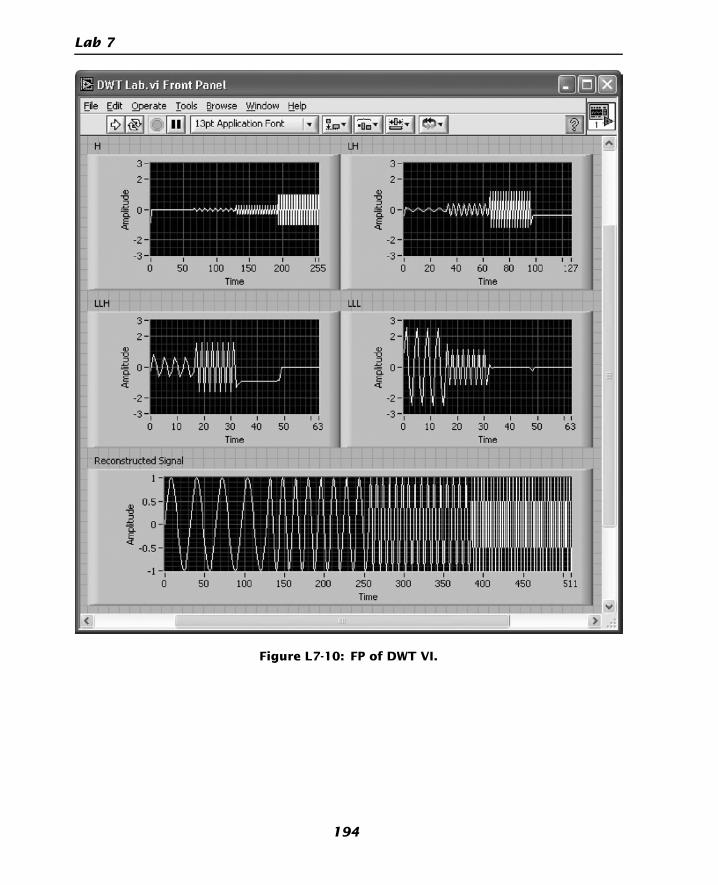
Figure L7-10: FP of DWT VI.
194
Lab 7

L7.3 Bibliography
[1] C. Burrus, R. Gopinath, and H. Gao, Wavelets and Wavelet Transforms—A Primer, Prentice-Hall, 1998.
[2] National Instruments, Signal Processing Toolset User Manual, Part Number322142C-01, 2002.
[3] National Instruments, LabVIEW User Manual, Part Number 320999E-01,2003.
L7.4 Lab Experiments
1. Build a VI to show the difference between the FFT and STFT transformations ona 512-point composite signal consisting of the following four components addedtogether: (i) a 215 Hz sinusoidal signal sampled at 1200 Hz, (ii) a 125 Hz sinu-soidal signal sampled at 1200 Hz with a phase shift of 90 degrees, (iii) a chirpsignal sampled at 1200 Hz with linearly increasing frequency from 150 Hz to200 Hz, and (iv) an impulse signal having an amplitude of 5 at the 75th and240th samples. Generate the composite signal with and without using theMathScript feature. For each case, compute and display both FFT and STFT.Observe the STFT output for varying levels of frequency bins and time windowwidths. Also, compare the STFT output for different user-defined windows suchas Hanning and Hamming windows.
2. Build a VI to show the difference between the FFT and STFT transformations on a512-point composite signal consisting of the following four components addedtogether: (i) a 175 Hz sinusoidal signal sampled at 1500 Hz, (ii) a 225 Hz sinusoidalsignal sampled at 1500Hz with a phase shift of 90 degrees, (iii) a chirp signal sampledat 1500 Hz with linearly increasing frequency from 350–425 Hz, and (iv) an impulsesignal having an amplitude of 10 at the 165th and 235th samples. Generate thecomposite signal with and without using the MathScript feature. For each case,compute and display both FFT and STFT. Observe the STFT output for varyinglevels of frequency bins and time window widths. Also, compare the STFT output fordifferent user-defined windows such as Chebyshev and Kaiser-Bessel windows.
3. Build a VI to show the four-level DWT transformation on a 512-point compositesignal consisting of four components each having 128 samples, namely threesinusoidal signals with increasing frequencies 125 Hz, 235Hz, 455Hz, and a chirpsignal with linearly increasing frequency from 500 Hz to 700 Hz. Use a sampling
195
FFT, STFT, and DWT

frequency of 8000 Hz. Generate the composite signal with and without using theMathScript feature. For each case, compute and display the four-level waveletdecomposition and reconstruction of the composite signal.
4. Build a VI to show the five-level DWT transformation on a 512-point compositesignal consisting of four components each having 128 samples, namely threesinusoidal signals with increasing frequencies 165 Hz, 295Hz, 575Hz, and a chirpsignal with linearly increasing frequency from 700 Hz to 900 Hz. Use a samplingfrequency of 8000 Hz. Generate the composite signal with and without usingthe MathScript feature. Also, extract the wavelet decomposed outcomes for eachstage of the filter bank with and without using the MathScript feature. For eachcase, compute and display the five-level wavelet decomposition and reconstruc-tion of the composite signal.
196
Lab 7

CHAPTER8DSP Implementation Platform:TMS320C6x Architecture and
Software Tools
Implementing some or most components of a signal processing system on a DSPprocessor is often computationally more efficient. The choice of a DSP processor touse in a signal processing system is application dependent. Many factors influencethis choice, including cost, performance, power consumption, ease-of-use, time-to-market, and integration/interfacing capabilities.
8.1 TMS320C6X DSP
The family of TMS320C6x processors, manufactured by Texas Instruments, is builtto deliver speed. They are designed for a million instructions per second (MIPS)intensive applications such as digital video. There are many processor versionsbelonging to this family differing in instruction cycle time, speed, power con-sumption, memory, peripherals, packaging, and cost. For example, the fixed-pointC6416-600 version operates at 600 MHz (1.67 ns cycle time), delivering a peakperformance of 4800 MIPS. The floating-point C6713-225 version operates at 225MHz (4.4 ns cycle time), delivering a peak performance of 1350 MIPS.
Figure 8-1 shows a block diagram of the generic C6x architecture. The C6x centralprocessing unit (CPU) consists of eight functional units divided into two sides: Aand B. Each side has an .M unit (used for multiplication operation), an .L unit (usedfor logical and arithmetic operations), an .S unit (used for branch, bit manipulation,and arithmetic operations), and a .D unit (used for loading, storing, and arithmeticoperations). Some instructions such as ADD can be done by more than one unit.Sixteen 32-bit registers are associated with each side. Interaction with the CPU mustbe done through these registers.
197

As shown in Figure 8-2 the internal buses consist of a 32-bit program address bus, a256-bit program data bus accommodating eight 32-bit instructions, two 32-bit dataaddress buses (DA1 and DA2), two 32-bit (64-bit for C64 version) load data buses(LD1 and LD2), and two 32-bit (64-bit for the floating-point version) store databuses (ST1 and ST2). In addition, there are a 32-bit direct memory access (DMA)data and a 32-bit DMA address bus. The off-chip, or external, memory is accessedthrough a 20-bit address bus and a 32-bit data bus.
The peripherals on a typical C6x processor include External Memory Interface(EMIF), DMA, Boot Loader, Multi-channel Buffered Serial Port (McBSP), HostPort Interface (HPI), Timer, and Power Down unit. EMIF provides the necessarytiming for accessing external memory. DMA allows the movement of data from oneplace in memory to another place without interfering with the CPU operation.Boot Loader boots the code from off-chip memory or HPI to the internal memory.McBSP provides a high-speed multi-channel serial communication link. HPI allowsa host to access the internal memory. Timer provides two 32-bit counters. ThePower Down unit is used to save power for durations when the CPU is inactive.
8.1.1 Pipelined CPU
In general, there are three basic steps to perform an instruction. They includefetching, decoding, and execution. If these steps are done serially, not all of theresources on the processor, such as multiple buses or functional units, are fullyutilized. In order to increase throughput, DSP CPUs are designed to be pipelined.
ExternalMemory
-Sync
-Async
Addr
D(32)EMIF
Program RAM Data RAM
DMA
Serial Port
Host Port
Boot Load
Timers
Pwr Down
Internal Buses
Reg
s (A
0-A
15) R
egs (B0-B
15)
.D1 .D2
.M2.M1
.L1 .L2
.S2.S1
Control Regs
Figure 8-1: Generic C6x architecture.
198
Chapter 8

This means that the foregoing steps are carried out simultaneously. Figure 8-3illustrates the difference in the processing time for three instructions executed on aserial or non-pipelined and a pipelined CPU. As one can see from this figure, a pipe-lined CPU requires fewer clock cycles to complete the same number of instructions.
The C6x architecture is based on the Very Long Instruction Word (VLIW)architecture. In such architectures, several instructions are captured and processedsimultaneously. For more details on the TMS320C6000 architecture, the interestedreader is referred to [1].
8.1.2 C64x DSP
The C64x is a more recently released DSP core, as part of the C6x family, withhigher MIPS power operating at higher clock rates. This core can operate in therange of 300–1000 MHz clock rates, giving a processing power of 2400–8000 MIPS.The C64x speedups are achieved due to many enhancements, some of which arementioned here.
InternalMemory
Addr �32
Data �32
Data �32
Data �32
Addr �32
Addr
ExternalMemory
Peripherals
Program Addr
Program Data
�32
�32
�32
�32
�32
�32
�32
�32/64
�32/64
�32/64
�32/64
�256
Data Addr - A (DA1)
Data Addr - B (DA2)
Load Data - A (LD1)
Store Data - A (ST1)
Load Data - B (LD2)
Store Data - B (ST2)
DMA Addr - Read
DMA Data - Read
DMA Addr - Write
DMA Data - Write
.D1
.D2
DMA
Figure 8-2: C6x internal buses.
199
DSP Implementation Platform: TMS320C6x Architecture and Software Tools

Per CPU data path, the number of registers is increased from 16 to 32, A0–A31 andB0–B31. These registers support packed data types, allowing storage andmanipulation of four 8-bit or two 16-bit values within a single 32-bit register.
Although the C64x core is code compatible with the earlier C6x cores, it can runadditional instructions on packed data types, boosting parallelism. For example, thenew instruction MPYU4 performs four, or quad, 8-bit multiplications, or theinstruction MPY2 performs two, or dual, 16-bit multiplications in a singleinstruction cycle on an .M unit. This packed data processing capability is illustrated inFigure 8-4.
Additional instructions have been added to each functional unit on the C64x forperforming special-purpose functions encountered in wireless and digital imagingapplications. In addition, the functionality of each functional unit on the C64x hasbeen improved, leading to a greater orthogonality, or generality, of operations. Forexample, the .D unit can perform 32-bit logical operation just as the .S and .L units,or the .M unit can perform shift and rotate operations just as the .S unit.
CPU Type
Non-Pipelined
Pipelined
1 2 3 4 5 6 7 8 9
F1
F1
D1
D1
D2F2
F3
E1
E1
E2
E3D3
F2 D2 E2 F3 D3 E3
Fx = fetching of instruction x
Dx = decoding of instruction x
Ex = execution of instruction x
Clock Cycles
Figure 8-3: Pipelined versus non-pipelined CPU.
8 bit
32 32
8�8 8�8 8�8 8�8
161616 16
16�16 16�16OR
32
32 32
32
16 bit
Figure 8-4: C64x packed data processing capability.
200
Chapter 8

8.2 C6x DSK Target Boards
Upon the availability of a DSP Starter Kit (DSK) board, appropriate components ofa DSP system can be run on an actual C6x processor.
8.2.1 Board Configuration and Peripherals
As shown in Figure 8-5, the C6713 DSK board is a DSP platform which includes aC6713 floating-point DSP chip operating at 225 MHz with 8 Mbytes of on-boardsynchronous dynamic RAM (SDRAM), 512 Kbytes of flash memory, and a 16-bitstereo codec AIC23. The codec is used to convert an analog input signal to a digitalsignal for the DSP manipulation. The sampling frequency of the codec can bechanged from 8 kHz to 96 kHz. The C6416 DSK board includes a C6416 fixed-pointDSP chip operating at 600 MHz with 16 Mbytes of on-board SDRAM, 512 Kbytes offlash memory, and an AIC23 codec.
PowerJack
USBPort
DIPSwithces
LEDs ResetSwitch
ConfigSwitch
ExternalJTAG
HurricaneHeader
Line In Mic In
HeadphoneLine Out
Figure 8-5: C6713 DSK board [2].
201
DSP Implementation Platform: TMS320C6x Architecture and Software Tools

8.2.2 Memory Organization
The external memory used by a DSP processor can be either static or dynamic. Staticmemory (SRAM) is faster than dynamic memory (DRAM), but it is moreexpensive because it takes more space on silicon. SDRAM (synchronous DRAM)provides a compromise between cost and performance.
Given that the address bus is 32 bits wide, the total memory space of C6x consists of232 ¼ 4 Gbytes. For the lab exercises in this book, the DSK board is configured basedon the memory map 1 shown in Figure 8-6.
Address Memory Map 1
Internal RAM (L2)0000 64K
Reserved0000 24M
EMIF control regs0000 32
Cache Configuration regs0000 4
L2 base addr & count regs4000 32
L2 flush & clean regs5000 32
CE0 mem attribute regs8200 16
CE1 mem attribute regs8240 16
CE2 mem attribute regs8280 16
CE3 mem attribute regs82C0 16
HPI control regs0000 4
McBSP0 regs0000 40
McBSP1 regs0000 40
Timer0 regs0000 12
Timer1 regs0000 12
Interrupt selector regs0000 12
EDMA parameter RAM0000 2M
EDMA control regsFFE0 32
QDMA regs0000 20
QDMA pseudo-regs0020 20
McBSP0 data0000 64M
McBSP1 data0000 64M
CE0, SDRAM 16M
CE1, 8-bit ROM
0000
0000 128K
CE1, 8-bit I/O port 4
CE2-Daughtercard 256M
CE3-Daughtercard
0000
0000
0000
0000
256M
L1 base addr & count regs4020
0000
0001
0180
0184
0184
0184
0184
0184
0184
0184
0188
018C
0190
0194
0198
019C
01A0
01A0
0200
0200
3000
3400
8000
9000
9008
A000
B000
10000
0184 32
Block Size(Bytes)
Figure 8-6: C6x DSK memory map [3].
202
Chapter 8

If a program fits into the on-chip or internal memory, it should be run from there toavoid delays associated with accessing off-chip or external memory. If a program istoo big to be fitted into the internal memory, most of its time-consuming portionsshould be placed into the internal memory for efficient execution. For repetitivecodes, it is recommended that the internal memory is configured as cache memory.This allows accessing external memory as seldom as possible and hence avoidingdelays associated with such accesses.
8.3 DSP Programming
Most DSP processors can be programmed either in C or assembly. Although writingprograms in C would require less effort, the efficiency achieved is normally lessthan that of programs written in assembly. Efficiency means having as few instruc-tions or as few instruction cycles as possible by making maximum use of the resourceson the chip.
In practice, one starts with C coding to analyze the behavior and functionality of analgorithm. Then, if the required processing time is not met by using the C compileroptimizer, the time-consuming portions of the C code are identified and convertedinto assembly, or the entire code is rewritten in assembly. In addition to C andassembly, the C6x allows writing code in linear assembly. Figure 8-7 illustrates codeefficiency versus coding effort for three types of source files on the C6x: C, linearassembly, and hand-optimized assembly. As one can see, linear assembly provides agood compromise between code efficiency and coding effort.
C
LinearASM
ASM
CompilerOptimizer
AssemblyOptimizer
HandOptimized
TypicalEfficiency
CodingEffort
50-80%
80-100%
100%
Low
Med
High
Figure 8-7: Code efficiency versus coding effort [1].
203
DSP Implementation Platform: TMS320C6x Architecture and Software Tools

More efficient codes are obtained by performing assembly programming fully utilizingthe pipelined feature of the CPU. Details regarding programming in assembly/linearassembly and code optimization are discussed in [1].
8.3.1 Software Tools: Code Composer Studio
The assembler is used to convert an assembly file into an object file (.obj extension).The assembly optimizer and the compiler are used to convert, respectively, a linearassembly file and a C file into an object file. The linker is used to combine objectfiles, as instructed by the linker command file (.cmd extension), into an executablefile. All the assembling, linking, compiling, and debugging steps have beenincorporated into an integrated development environment (IDE) called CodeComposer Studio (CCS or CCStudio). CCS provides an easy-to-use graphical userenvironment for building and debugging C and assembly codes on various targetDSPs. Figure 8-8 shows the steps involved in going from a source file (.c extensionfor C, .asm for assembly, and .sa for linear assembly) to an executable file (.outextension).
During its setup, CCS can be configured for different target DSP boards (e.g., C6713DSK, C6416 DSK, C6xxx Simulator). The version used in the book is CCS 3.0.CCS provides a file management environment for building application programs.It includes an integrated editor for editing C and assembly files. For debugging
.out.obj
Code Composer Studio
.asm
.sa
.c
.c = C source file
.sa = linear assembly source file
.asm = assembly source file
.obj = object file
.out = executable file
.cmd = linker command file
TextEditor
Compiler
AssemblyOptimizer
Assembler Linker Debugging
Link.cmd
Figure 8-8: C6x software tools [1].
204
Chapter 8

purposes, it provides breakpoints, data monitoring and graphing capabilities, profilerfor benchmarking, and probe points to stream data to and from a target DSP.
8.3.2 Linking
Linking places code, constant, and variable sections into appropriate locations inmemory as specified in a linker command file. Also, it combines several object filesinto a final executable file. A typical command file corresponding to the DSKmemory map 1 is shown in Figure 8-9.
The first part, MEMORY, provides a description of the type of physical memory, itsorigin and its length. The second part, SECTIONS, specifies the assignment ofvarious code sections to the available physical memory. These sections are definedby directives such as .text, .data, etc.
8.3.3 Compiling
The build feature of CCS can be used to perform the entire process of compiling,assembling, and linking in one step. The compiler allows four levels of optimizations.
Debugging and full-scale optimization cannot be done together, since they are inconflict; that is, in debugging, information is added to enhance the debugging
Figure 8-9: A typical command file.
205
DSP Implementation Platform: TMS320C6x Architecture and Software Tools

process, whereas in optimizing, information is minimized or removed to enhancecode efficiency. In essence, the optimizer changes the flow of C code, makingprogram debugging very difficult.
It is thus a good programming practice to first verify the proper functionality of codesby using the compiler with no optimization. Then, use full optimization to makethem efficient. It is recommended that an intermediary step be taken in whichsome optimization is done without interfering with source-level debugging.This intermediary step can re-verify code functionality before performing fulloptimization.
8.4 Bibliography
[1] N. Kehtarnavaz, Real-Time Digital Signal Processing Based on theTMS320C6000, Elsevier, 2005.
[2] Texas Instruments “C6713 DSK Tutorial,” Code Composer Studio 2.2 C6713DSK Help, 2003.
[3] Texas Instruments, TMS320C6711, TMS320C6711B, TMS320C6711C,TMS320C6711D Floating-Point Digital Signal Processors, SPRS088L, 2004.
206
Chapter 8

Lab 8: Getting Familiar withCode Composer Studio
L8.1 Code Composer Studio
This tutorial lab introduces the basic features of CCS one needs to know in order tobuild and debug a C program running on a DSP processor. To become familiarwith all of its features, refer to the TI CCS Tutorial [1] and TI CCS User’s Guidemanuals [2].
This lab demonstrates how a simple DSP program can be compiled and linked byusing CCS. The algorithm consists of a sinewave generator via using a differenceequation. As part of this example, debugging and benchmarking issues are alsocovered. Knowledge of C programming is required for this and the next lab. Theselabs may be skipped if the reader is interested only in the LabVIEW implementation.
Note that the accompanying CD provides the lab programs separately for the DSPtarget boards C6416 and C6713 DSK, as well as the simulator.
L8.2 Creating Projects
Let us consider all the files required to create an executable file; that is, .c (c),.asm (assembly), and .sa (linear assembly) source files; a .cmd linker commandfile; an .h header file; and appropriate .lib library files. The CCS code develop-ment process begins with the creation of a project to easily integrate and manageall these required files for generating and running an executable file. After openingCCS by double-clicking the CCS icon on the desktop, one can see the ProjectView panel on the left side of the CCS window. This panel provides an easymechanism for building a project. In this panel, a project file (.pjt extension) canbe created or opened to contain not only the source and library files, but also thecompiler, assembler, and linker options for generating an executable file.
To create a project, choose the menu item Project » New from the CCS menu bar.This brings up the dialog box Project Creation, as shown in Figure L8-1. In thedialog box, navigate to the working folder, here considered to be C:\CCStudio\myprojects, and type a project name in the field Project Name. Then, click the buttonFinish for CCS to create a project file named Lab08.pjt. All the files necessary to runa program should be added to the project.
207

CCS provides an integrated editor which allows the creation of source files. Someof the features of the editor are color syntax highlighting, code block marking inparentheses and braces, parenthesis/brace matching, control indentions, andfind/replace/search capabilities. It is also possible to add files to a project fromWindows Explorer using the drag-and-drop approach. An editor window isbrought up by choosing the menu item File » New » Source File. For this lab,let us type the following C code into the editor window:
#include <stdio.h>#include <math.h>
#define PI 3.141592
void main(){
short i, gain;float fs, f;float y[3], a[2], b1, x;
short *output;output = (short *) 0x0000FF00;
// Coefficient Initialization
fs = 8000; // Sampling frequencyf = 500; // Signal frequencygain = 100; // Amplitude gain
Figure L8-1: Creating a new project.
208
Lab 8

a[0] = -1;a[1] = 2 * cos(2*PI*f/fs);b1 = gain;
// Initial Conditions
y[1] = y[2] = 0;x = 1;
printf("BEGIN\n");
for (i=0; i<128; i++){
y[0] = b1*x + a[1]*y[1] + a[0]*y[2];y[2] = y[1];y[1] = y[0];x = 0;
output[i] = (short) y[0];}printf("END\n");
}
This code generates a sinusoidal waveform y½n� based on the following differenceequation:
y½n� ¼ B1x½n� 1� þ A1y½n� 1� þ A0y½n� 2� (8.1)
where B1 ¼ 1, A0 ¼ �1, A1 ¼ 2 cos ðyÞ, and x½n� is a delta function. The frequencyof the waveform is given by [1]
f ¼ fs2p
arccos ðA1=2Þ (8.2)
By changing the coefficient A1, one can alter the frequency. By changing the coef-ficient B1, one can alter the gain.
Save the created source file by choosing the menu item File » Save. This brings upthe dialog box Save As, as shown in Figure L8-2. In the dialog box, go to the fieldSave as type and select C Source Files (*.c) from the pull-down list. Then, go to thefield File name and type sinewave.c. Finally, click Save to save the code into a Csource file named sinewave.c.
209
Getting Familiar with Code Composer Studio

In addition to source files, a linker command file must be specified to createan executable file and to conform to the memory map of the target DSP.A linker command file can be created by choosing File » New » Source File. Forthis lab, let us type the command file shown in Figure L8-3. This file can also bedownloaded from the accompanying CD, which is configured based on the DSKmemory map. Save the editor window into a linker command file by choosingFile » Save or by pressing <Ctrl-S>. This brings up the dialog box Save As.Go to the field Save as type and select TI Command Language Files (*.cmd)from the pull-down list. Then, type Lab08.cmd in the field File name andclick Save.
Figure L8-2: Creating a source file.
210
Lab 8

Now that the source file sinewave.c and the linker command file Lab08.cmd arecreated, they should be added to the project for compiling and linking. To do this,choose the menu item Project » Add Files to Project. This brings up the dialog boxAdd Files to Project. In the dialog box, select sinewave.c and click the button Open.This adds sinewave.c to the project. In order to add Lab08.cmd, choose Project » AddFiles to Project. Then, in the dialog box Add Files to Project, set Files of type toLinker Command File (*.cmd) so that Lab08.cmd appears in the dialog box. Next,select Lab08.cmd and click the button Open. In addition to sinewave.c and Lab08.cmdfiles, the run-time support library should be added to the project. To do so,choose Project » Add Files to Project, go to the compiler library folder (here assumed tobe the default option C:\CCStudio\c6000\cgtools\lib), select Object and LibraryFiles (*.o*,*.l*) in the box Files of type, then select rts6700.lib, and click Open.If running on the TMS320C6416, select rts6400.lib instead.
After one adds all the source files, the command file, and the library file to theproject, it is time to either build the project or to create an executable file for thetarget DSP. This is achieved by choosing the Project » Build menu item. CCScompiles, assembles, and links all of the files in the project. Messages about thisprocess are shown in a panel at the bottom of the CCS window. When the buildingprocess is completed without any errors, the executable file Lab08.out is generated.It is also possible to do incremental builds—that is, rebuilding only those files
Figure L8-3: Linker command file for Lab 8.
211
Getting Familiar with Code Composer Studio

changed since last build—by choosing the menu item Project » Rebuild. The CCSwindow provides shortcut buttons for frequently used menu options, such asIncremental Build and Rebuild All .
Although CCS provides default build options, all the compiler, assembler, and linkeroptions can be changed via the menu item Project » Build Options. Among manycompiler options shown in Figure L8-4, particular attention should be paid to theoptimization level options. There are four levels of optimization (0, 1, 2, 3), whichcontrol the type and degree of optimization. Note that in some cases, debuggingis not possible due to optimization. Thus, it is recommended to first debug a programto make sure that it is logically correct before performing any optimization.
Figure L8-4: Build and compiler options.
212
Lab 8

Another important compiler option is the Target Version option. When imple-menting on the floating-point target DSP (TMS320C6713 DSK), go to the TargetVersion field and select C671x (-mv6710) from the pull-down list. For the fixed-pointtarget DSP (TMS320C6416 DSK), select C64xx (-mv6400).
When a message stating a compilation error appears, click Stop Build and scroll up inthe build area to see the syntax error message. Double-click on the red text thatdescribes the location of the syntax error. Notice that the sinewave.c file opens, andthe cursor appears on the line that has caused the error, as shown in Figure L8-5.After one corrects the syntax error, the file should be saved and the project rebuilt.
Figure L8-5: Build error.
213
Getting Familiar with Code Composer Studio

L8.3 Debugging Tools
Once the build process is completed without any errors, the program can be loadedand executed on the target DSP. To load the program, choose File » Load Program,select the program Lab08.out just rebuilt, and click Open. To run the program,choose the menu item Debug » Run. One should be able to see BEGIN and ENDappearing in the Stdout window.
Now, let us view the content of the memory at a specific location. To do so, selectView » Memory from the menu. The Memory Window panel should appear on the rightside of the CCS window. Select 16-bit Signed Int from the pull-down list at thebottom of the panel. Then, type 0x0000FF00 in the Address field and press Enter.A memory window grid should appear in the middle of the panel, as shown inFigure L8-6. The contents of the CPU, peripheral, DMA, and serial port registerscan also be viewed by selecting View » Registers » Core Registers.
Data stored in the DSP memory can be saved to a file. CCS provides a probe pointcapability so that a stream of data can be moved from the DSP to a PC host file orvice versa. In order to use this capability, one should set a probe point within the
program by placing a mouse cursor at the line where a stream of data needs to be
transferred and by clicking the button Probe Point (see Figure L8-7). Choose
File » File I/O to invoke the dialog box File I/O, as shown in Figure L8-8. Select the tabFile Output for saving the data file; then click the button Add File and type the nameof the data file. Next, the file should be connected to the probe point by clicking thebutton Add Probe Point. In the Probe Point field, select the probe point to make itactive; then connect the probe point to the PC file through File Out:. . . in the fieldConnect To. Click the button Replace and then the button OK.
Figure L8-6: Memory Window Options dialog box and memory window.
214
Lab 8

Figure L8-7: Probe Points window.
Figure L8-8: File I/O window.
215
Getting Familiar with Code Composer Studio

Finally, enter the memory location in the Address field and the data type in theLength field. For storing the data in short format, 64 words need to be stated in thelength field for 128 short data. A probe point connected to a PC file is shown inFigure L8-8. The probe point capability can be used to simulate the execution of aprogram in the absence of a live signal. A valid PC file should have the correct fileheader and extension. The file header should conform to the following format:
MagicNumber Format StartingAddress PageNum Length
MagicNumber is fixed at 1651. Format indicates the format of samples in the file:1 for hexadecimal, 2 for integer, 3 for long, and 4 for float. StartingAddressand PageNum are determined by CCS when a stream of data is saved into a PCfile. Length indicates the number of samples in memory. A valid data file shouldhave the extension .dat. Data files having the same format can be transferred bychoosing File » Data » Load. . . instead. However, data transfer with this capabilityof CCS needs to be activated manually, whereas the probe point does data updatesautomatically.
A graphical display of data often provides better feedback about the behavior of aprogram. CCS provides a signal analysis interface to monitor a signal. Let usdisplay the array of values at 0x0000FF00 as a signal or a time graph. To do so, selectView » Graph » Time/Frequency to view the Graph Property Dialog box. Field namesappear in the left column. Go to the Start Address field, click it, and type0x0000FF00. Then, go to the Acquisition Buffer Size field, click it, and enter 128.Also, enter 128 in the Display Data Size field. Finally, click on DSP Data Type,select 16-bit signed integer from the pull-down list, and click OK (see Figure L8-9).A graph window appears based on the properties selected. This window is illustratedin Figure L8-10. Properties of the graph window can be changed by right-clickingon it and selecting Properties at any time during the debugging process.
To access a specific location of the DSP memory, one can assign a memoryaddress directly to a pointer. It is necessary to typecast the pointer to shortbecause the values are of that type. In the code shown, a pointer is assignedto 0x0000FF00.
When developing and testing programs, one often needs to check the value of avariable during program execution. This can be achieved by using breakpointsand watch windows. To view the values of the pointer in sinewave.c before andafter the pointer assignment, choose File » Reload Program to reload the program.
216
Lab 8

Then, double-click on sinewave.c in the Project View panel to bring up the source file,as shown in Figure L8-11. You may wish to make the window larger to see more of thefile in one place. Next, put the cursor on the line that reads output ¼ (short *)0x0000FF00 and press <F9> to set a breakpoint. To open a watch window, choose
Figure L8-9: Graph Property Dialog box.
Figure L8-10: Graphical Display window.
217
Getting Familiar with Code Composer Studio

View » Watch Window from the menu bar. This will bring up a watch window withthe local variables listed in theWatch Locals tab. To add a new expression to the watchwindow, select the Watch 1 tab; then type output (or any expression you desire toexamine) in the Name column. Then, choose Debug » Run or press<F5>. The programstops at the breakpoint and the watch window displays the value of the pointer. This isthe value before the pointer is set to 0x0000FF00. By pressing <F10> to step over theline, or the shortcut button , one should be able to see the value 0x0000FF00 in thewatch window.
To add a C function that sums the values, one can simply pass a pointer to an arrayand have a return type of integer. The following C function can be used to sumthe values and return the result:
#include <stdio.h>#include <math.h>
#define PI 3.141592
void main(){
short i, gain;int ret;
Figure L8-11: Project View panel.
218
Lab 8

float fs, f;float y[3], a[2], b1, x;
short *output;output = (short *) 0x0000FF00;
// Coefficient Initializationfs = 8000; // Sampling frequencyf = 500; // Signal frequencygain = 100; // Amplitude gain
a[0] = -1;a[1] = 2 * cos(2*PI*f/fs);b1 = gain;
// Initial Conditions
y[1] = y[2] = 0;x = 1;
printf("BEGIN\n");
for (i=0; i<128; i++){
y[0] = b1*x + a[1]*y[1] + a[0]*y[2];y[2] = y[1];y[1] = y[0];x = 0;
output[i] = (short) y[0];}ret = sum(output,128);
printf("Sum = %d\n", ret);printf("END\n");
}int sum(const short* array,int N){
int count,sum;sum = 0;
for(count=0 ; count<N ; count++)sum += array[count];
return(sum);}
219
Getting Familiar with Code Composer Studio

As part of the debugging process, it is normally required to benchmark or time aprogram. In this lab, let us determine how much time it takes for the function sum()to run. To achieve this benchmarking, reload the program and choose Profile » Setup.
This will bring up the Profile Setup panel. Click at the top of the panel to enable
profiling. Then, click to enable profiling of all the functions. To view and modify
the profiling function list, switch to the Ranges tab. Remove the unnecessaryfunction main() from the list by highlighting the function name under Function »Enabled and press the spacebar. Notice that the function main() now appears ingray under Function » Disabled. Finally, press <F5> to run the program andchoose Profile » Viewer to examine the number of cycles for sum(), as shown inFigure L8-12 (the exact number may vary slightly from the one shown). This is thenumber of cycles it takes to execute the function sum().
There is another way to benchmark codes using breakpoints. Double-click on the filesinewave.c in the Project View panel and choose View » Mixed Source/ASM to list theassembled instructions corresponding to the C code lines. Set a breakpoint at thecalling line by placing the cursor on the line that reads ret ¼ sum(point,128);then press <F9> or double-click Selection Margin located on the left side of theeditor. Set another breakpoint at the next line, as indicated in Figure L8-13. Oncethe breakpoints are set, choose Profile » Clock » Enable to enable a profiler clock.
Then, choose Profile » Clock » View, and a Profile Clock icon will appear at the
lower right corner of the CCS window. Press <F5> to run the program. When theprogram is stopped at the first breakpoint, reset the clock by double-clicking theProfile Clock icon. Finally, click Step Out or Run in the Debug menu to execute andstop at the second breakpoint. Examine the number of clock cycles displayed on theright side of the icon. It should be close to the breakpoint approach. The differencein the number of cycles between the breakpoint and the profile approaches is origi-nated from the extra procedures for calling functions, e.g., passing arguments tofunction, storing return address, branching back from function, etc.
Figure L8-12: Profile window.
220
Lab 8

A workspace containing breakpoints, streaming data, graphs, and watch windowscan be stored and recalled later. To do so, choose File » Workspace » Save WorkspaceAs. This will bring up the Save Workspace window. Type the workspace name in theFile name field; then click Save.
Table L8-1 provides the number of cycles needed to run the sum() function usingseveral different builds. When a program is too large to fit into the internalmemory, it has to be placed into the external memory. Although the program in thislab is small enough to fit in the internal memory, it is also placed in the externalmemory to show the change in the number of cycles. To move the program intothe external memory, open the command file Lab08.cmd and replace the line.text > PMEM with .text > BMEM. As seen in Table L8-1, this build slows
Table L8-1: Number of Cycles for Different Builds
Type of Build Number of Cycles
C program in external memory 82573
C program in internal memory 3998
-o0 1838
-o1 1814
-o2 172
Figure L8-13: Profiling code execution time using breakpoints.
221
Getting Familiar with Code Composer Studio

down the execution to 82573 cycles. In the second build, the program resides inthe internal memory, and the number of cycles is hence reduced to 3998. Byincreasing the optimization level, one can further decrease the number of cycles to172. At this point, it is worth pointing out that the stated numbers of cycles inthis lab correspond to the C6713 DSK with the CCS version 3.0. One shouldrealize that the numbers of cycles will vary depending on the DSK target boardand CCS version used.
L8.4 Bibliography
[1] Texas Instruments, TMS320C6000 Code Composer Studio Tutorial, LiteratureID# SPRU 301C, 2000.
[2] Texas Instruments, Code Composer Studio User’s Guide, Literature ID# SPRU328B, 2000.
222
Lab 8

CHAPTER9LabVIEW DSP Integration
A DSP system designed in LabVIEW can be placed entirely or partially on ahardware platform. This chapter discusses the implementation process on a DSPhardware platform consisting of a TMS320C6713 or TMS320C6416 DSK board.Such an implementation or integration is made possible by using the LabVIEWtoolkit DSP Test Integration for TI DSP.
9.1 Communication with LabVIEW: Real-Time Data Exchange(RTDX)
Communication between LabVIEW and a C6x DSK board is achieved by using theReal-Time Data Exchange (RTDX™) feature of the TMS320C6x DSP. This featureallows one to exchange data between a DSK board and a PC host (runningLabVIEW) without stopping program execution on the DSP side. This dataexchange is done either via the Joint Test Action Group (JTAG) connection orthe Universal Serial Bus (USB) port emulating the JTAG connection.
RTDX can be configured in two modes: non-continuous and continuous. In non-continuous mode, data are written to a log file on the host. This mode is normallyused for recording purposes. In continuous mode, data are buffered by the RTDXhost library. This mode is normally used for continuously displaying data. Here, sothat one can view the processed data on the PC/LabVIEW side, RTDX is configuredto be in continuous mode.
9.2 LabVIEW DSP Test Integration Toolkit for TI DSP
The DSP Test Integration for TI DSP toolkit provides a set of VIs which enableinterfacing between LabVIEW and Code Composer Studio [1]. The VIs provided in
223

this toolkit are categorized into two groups: CCS Automation and CCS Communi-cation. These VI groups are listed in Table 9-1.
The VIs in the CCS Automation group allow automating the CCS code executionsteps through LabVIEW. They include (a) open CCS, (b) build project, (c) resetCPU, (d) load program, (e) run code, (f) halt CPU, and (g) close CCS. The flow ofthese steps is the same as those in CCS.
The VIs in the CCS Communication group allow exchange of data throughthe RTDX channel. For example, the CCS RTDX write VI and CCS RTDXread VI are used for writing and reading data to and from the DSP side,respectively. Note that these VIs are polymorphic. Therefore, data types(i.e., single precision, double precision, or integer) and data formats (i.e., scalaror array) should be matched in LabVIEW and CCS in order to establish aproper LabVIEW DSP integration.
9.3 Combined Implementation: Gain Example
In this section, a LabVIEW DSP integration example is presented to show thebasic steps that are required for a combined LabVIEW and DSP implementation.From the main dialog box of LabVIEW, open the NI Example Finder, shown inFigure 9-1, by choosing Help » Find Examples.
Table 9-1: List of VIs in the LabVIEW DSP Test Integration Toolkit
CCS Automation VIs CCS Communication VIs
CCS Open Project VI CCS RTDX Read VI
CCS Build VI CCS RTDX Write VI
CCS Download Code VI CCS RTDX Enable VI
CCS Run VI CCS RTDX Enable Channel VI
CCS Halt VI CCS RTDX Disable VI
CCS Close Project VI CCS RTDX Disable Channel VI
CCS Window Visibility VI CCS Memory Read VI
CCS Reset VI CCS Memory Write VI
CCS Symbol to Memory Address VI
224
Chapter 9

Open the Gain_dsk6713 VI by clicking on Directory Structure from the categoryBrowse according to of the Browse tab and by choosing DSPTest » dsk6713 » Gain »Gain_dsk6713.vi. If using a C6416 DSK, open the dsk6416 folder.
In this example, an input signal and a gain factor are sent from the LabVIEWside to the DSP side. On the DSP side, the input signal is multiplied by thegain factor and then sent back to the LabVIEW side. The gain factor, thefrequency of the input signal, and the signal type can be altered by the controlsspecified in the FP. Also, the original and scaled signals are displayed in the FP,as shown in Figure 9-2.
Figure 9-1: NI Example Finder—Gain example.
225
LabVIEW DSP Integration

9.3.1 LabVIEW Configuration
To better understand the LabVIEW DSP integration process, let us examine the BDof the Gain_dsk6713 VI, which is shown in Figure 9-3.
Two major sections are associated with this BD. The first section consisting of aStacked Sequence structure, shown to the left side of the While Loop,corresponds to the CCS automation process. This section includes a CCS OpenProject VI, a CCS Build VI, a CCS Reset VI, a CCS Download Code VI, anda CCS Run VI. In addition, a CCS Halt VI and a CCS Close Project VI,shown to the right side of the While Loop, are a part of the CCS automationprocess. The three functions (Strip Path, Build Path, and Current VI’sPath) of the File I/O palette (Functions » Programming » File I/O) are used in theStacked Sequence structure to create a file path to a CCS project file that can beopened from the CCS side. With these VIs and functions in place, the process ofopening CCS, building a project, loading a program to the DSP, and running it on
Figure 9-2: FP of Gain example.
226
Chapter 9

the DSP can be controlled from the LabVIEW side. The CCS Automation VIs arelocated in the DSP Test Integration Palette (Functions » Addons » DSP TestIntegration). Note that the CCS automation process just described can be used forall the LabVIEW DSP integration examples presented in Lab 9.
The second section of the BD shown in the While Loop involves signal generationand CCS RTDX communication. The Basic Function Generator VI(Functions » Signal Processing » Waveform Generation) is used to generate waveformsamples. Two CCS RTDX read VIs and one CCS RTDX write VI are located in theWhile Loop. The channel name of each CCS RTDX VI is wired to this VI.This allows the generated samples to be continuously sent to the DSP side, and theDSP processed samples to be continuously read from the DSP side. The scaled signalis displayed in a waveform graph. Note that the original and scaled signals are ofarray type, while the gain factor is scalar. Thus, one of the CCS RTDX read/writeVIs is set to 32-bit integer array, indicated by [I32]on its icon, and the other is setto 32-bit integer, indicated by I32 on its icon.
9.3.2 DSP Configuration
A CCS project implemented on the DSP side should include four components: alinker command file, an interrupt service table which defines the interrupt vector forRTDX, the RTDX library along with the run-time support library, and the sourcecode, as shown in Figure 9-4.
Figure 9-3: BD of Gain example.
227
LabVIEW DSP Integration

The C source code of the Gain example running on the DSP side is as follows:
#include <rtdx.h> /* RTDX */#include "target.h" /* TARGET_INITIALIZE() */
#define kBUFFER_SIZE 49
RTDX_CreateInputChannel(cinput);RTDX_CreateInputChannel(cgain);RTDX_CreateOutputChannel(coutput);
// Gain value scales the waveformvoid Gain (int *output, int *input, int gain){
int i;for(i=0; i<kBUFFER_SIZE; i++)
output[i]=input[i]*gain;}void main(){
int input[kBUFFER_SIZE];
Figure 9-4: Project view of CCS.
228
Chapter 9

int output[kBUFFER_SIZE];int gain = 10;
// Target initialization for RTDXTARGET_INITIALIZE();
/* enable RTDX channels */RTDX_enableInput(&cgain);RTDX_enableInput(&cinput);RTDX_enableOutput(&coutput);
for (;;) /* Infinite message loop. */{
/* Read new gain value if one exists */if (!RTDX_channelBusy(&cgain))
RTDX_readNB(&cgain, &gain, sizeof(gain));/* Wait for input waveform */while(!RTDX_read(&cinput, input, sizeof(input)));
Gain (output, input, gain);
/* Write scaled data back to host. */RTDX_write(&coutput, output, sizeof(output));
}}
In this code, several application programming interfaces (APIs), which are partof the CCS RTDX library, are used to allow data exchange between the DSP andLabVIEW side. First, the RTDX_CreateInputChannel() and RTDX_CreateOutputChannel() APIs are used to declare the input and outputchannels. Second, the DSP board is initialized with the TARGET_INITIALIZE()API. Both of the RTDX channels are enabled by the RTDX_enableInput()and RTDX_enableOutput() APIs. To get scalar data from the LabVIEWto the DSP side, one needs to use the RTDX_readNB() API, with the argumentsbeing channel, buffer pointer, and buffer size. In addition, one needs to usethe RTDX_read() API, with the arguments being channel, array pointer,and array size. The RTDX_write() API is used to send data back to theLabVIEW side.
Bear in mind that the name assigned to the RTDX communication channelshould be the same as the one used in LabVIEW. Also, the data types of polymorphicVIs, i.e., CCS RTDX Read VI and CCS RTDX Write VI, as well as the array
229
LabVIEW DSP Integration

lengths should be the same as the ones defined in LabVIEW. For example, theinput array input[]in the preceding source code should be defined asfollows:
int input[kBUFFER_SIZE];
That is, input[]must be declared as a 32-bit integer, and the array size must beconfigured to be kBUFFER_SIZE, which is specified as 49 at the beginning of theGain sample code.
9.4 Bibliography
[1] National Instruments, LabVIEW DSP Test Toolkit for TI DSP User’s Manual,Literature Number 323452A-01, 2002.
230
Chapter 9

Lab 9: DSP Integration Examples
This lab includes four DSP integration examples. These examples correspond to theDSP systems built by LabVIEW in the previous labs, i.e., digital filtering, integerarithmetic, adaptive filtering, and frequency processing.
L9.1 CCS Automation
Figure L9-1 illustrates the CCS automation process. In this lab, all the examplesare assumed to have the sub-diagrams shown to the left and right of the WhileLoop and thus are not explicitly mentioned.
Let us explain the CCS automation process in more detail. In order to specify a projectto be used by the CCS Automation VIs, one should build a file path to the project file.Two methods of creating a path are mentioned here. The first method involves usinga relative path by assuming that the CCS project file is located in the folder that theVI resides. Place a Current VI’s Path function (Functions » Programming » File I/O »File Constants » Current VI’s Path) in the BD to get the entire file path of the projectfile and wire the output of this VI to the path terminal of a Strip Path function(Functions » Programming » File I/O » Strip Path), which returns a stripped path byremoving the VI’s name from the path. The stripped path is wired to the base pathterminal of the Build Path function (Functions » Programming » File I/O » Build Path).This function appends the name of the file, wired to the name or relative path
Figure L9-1: Generic structure of CCS Automation.
231

terminal of the function as a string constant, to the stripped path. Now, the output ofthe function indicates the entire path of the CCS project file. The created file path isthen wired to the Path to Project terminal of the CCS Open Project VI toallow access by the CCS Automation VIs.
The second method of creating a project path involves using an absolute path. Wirea Path Constant (Functions » Programming » File I/O » File Constants » Path Constant)to the Path to Project terminal of the CCS Open Project VI or create a fileconstant by right-clicking and choosing Create » Constant on the Path to Projectterminal of the VI. Enter the absolute path of the CCS project file in the PathConstant. The absolute path can also be generated by browsing the project file path.To do this, right-click on the Path Constant and choose Browse for Path. . . from theshortcut menu. A file dialog box appears to select the path via file browsing.
Next, place the CCS Automation VIs (CCS Open Project VI, CCS BuildVI, CCS Reset VI, CCS Download Code VI, and CCS Run VI) from the DSPTest Integration Palette (Functions » Addons » DSP Test Integration) in the ordershown in Figure L9-1. These VIs are wired to each other via the terminals of theCCS references out (or dup CCS references) and error out to theterminals of the CCS references in and error in. The VIs are used to open aCCS project, build a project, reset CPU, download a program to the DSP, and runthe program. The CCS references cluster, wired to all the CCS Automation VIs,contains the CCS IDE references, while the error in/out cluster carries the errorinformation of the CCS Automation VIs. Consequently, if an error occurs in one ofthe CCS Automation VIs, the error information is passed through the CCSAutomation VIs to the Simple Error Handler VI (Functions » Programming »Dialog & User Interface » Simple Error Handler) located at the end of the CCSAutomation VIs. This VI displays a description of the error.
A String Indicator is placed in the FP in order to display the current statusof the CCS automation process. A Control Reference for this indicator iscreated by right-clicking on it and choosing Create » Reference from the shortcutmenu. This reference should be wired to the Status String Refnum terminal ofthe CCS Open Project VI in order to post a status string to this indicator.
Now, let us explain the exchange of data between LabVIEW and the DSP. Data arecontinuously exchanged using the CCS Communication VIs, CCS RTDX Read VIand CCS RTDX Write VI, when both the VI and CCS are running. As mentionedearlier, data types should be carefully configured on the LabVIEW and CCS sides,since the CCS RTDX Read VI and the CCS RTDX Write VI are data type poly-morphic. The read/write data type can be specified from the Select Type menu as partof the shortcut menu. This menu can be brought up by right-clicking on the CCS
232
Lab 9

RTDX Read VI or CCS RTDX Write VI. Another way to change the data type is touse a Polymorphic VI Selector. This selector can be displayed by right-clicking on itand choosing Visible Items » Polymorphic VI Selector from the shortcut menu. Thestring constants indicate the names of the RTDX channels that are wired to the CCSRTDX Read VI or CCS RTDX Write VI.
The execution of the While Loop structure is stopped by pressing a stop buttonin the FP or if an error is generated by the CCS Automation or CCSCommunication VIs. In such cases, the CCS needs to be halted and closed. Thisis done by locating and wiring a CCS Halt VI to a CCS Close Project VI.These VIs appear to the right side of the While Loop structure.
L9.2 Digital Filtering
In this section, the filtering code written in C is used to run the filtering blockor component of the Lab 4 filtering system on the DSP.
L9.2.1 FIR Filter
The BD of the FIR lowpass filtering system that was built in Lab 4 is illustratedin Figure L9-2.
Figure L9-2: Filtering system in Lab 4.
233
DSP Integration Examples

Let us modify this BD to send the generated samples to the DSP and then toreceive the filtered samples from the DSP. This is achieved by inserting the CCSautomation process to the left and right sections of the While Loop structure.As indicated in Figure L9-3, a portion of the DFD Filter VI is replaced with the CCSRTDX Write VI and the CCS RTDX Read VI. Both of these VIs are configuredto write and read single-precision floating-point array data, which means configuringthe polymorphic VIs as CCS RTDX Write Array SGL and CCS RTDX ReadArray SGL; refer to Figure L9-3. Consider that the number of samples in thesampling info cluster is reduced to 128 in order to reduce the time associated withthe RTDX communication.
An array of signal samples consisting of the sum of the three sinusoids is wired to theData terminal of the CCS RTDX Write Array SGL VI. Also, a string constantcontaining the name of the input channel, cinput, is wired to the Channelterminal.
Figure L9-3: BD of filtering system with DSP integration.
234
Lab 9

In the CCS RTDX Read Array SGL VI, the data transmitted via RTDX is readfrom the Data terminal of the VI. This terminal is wired to a waveform graphas well as to a Spectral Measurements Express VI for frequency analysis.
To check the status of errors generated by the CCS Automation or CCSCommunication VIs, observe the status element of the error cluster. Thisis made possible by locating an Unbundle By Name function (Functions »Programming » Cluster & Variant » Unbundle By Name). Wire the error out clusterfrom the CCS RTDX Read Array SGL VI to the Unbundle By Name function.This way, the status element of the error out cluster is selected by default.The result of an OR operation of two Boolean values, corresponding to thestatus element of the cluster and a stop button, is wired to the conditionalterminal of the While Loop. Whenever the stop button is pressed or an erroroccurs while accessing CCS or communicating via RTDX, the execution of theloop stops.
Notice the importance of the timeout value of the CCS RTDX Read Array SGL VI.If the RTDX communication speed is too slow or the number of data samples islarge, the timeout value should be changed to avoid getting an RTDX error, asshown in Figure L9-4. The default timeout value is 2000. To change the timeoutvalue, wire a Numeric Constant to the timeout terminal of the CCS RTDXRead Array SGL VI and enter a desired timeout value in milliseconds. Save thecompleted VI as DSP FIR Filtering System.vi.
Figure L9-4: RTDX error.
235
DSP Integration Examples

Next, let us discuss how to create a project in CCS. Create a new project and nameit FIR.pjt. Add the linker command file c6713dsk.cmd, the interrupt service vectorintvecs.asm, the source code FIR.c, and the library files rtdx.lib (CCStudio\C6000\rtdx\lib) and rts6700.lib (CCStudio\C6000\cgtools\lib) into the project. The linkercommand file and interrupt service vector are located in the folder DSK6713\Shared. This folder also includes the header file target.h. The path to this folder needsto be added in Include Search Path of Build Options, as shown in Figure L9-5.
Figure L9-5: Build Options of CCS.
236
Lab 9

It is worth mentioning that, if a C6416 DSK is used, the files and libraries to beadded to the project are different from those when using a C6713 DSK. Thecorresponding path of the linker command (c6416dsk.cmd) and interrupt servicevector (intvecs6416.asm) files for the DSK6416 board is DSK6416\Shared.The libraries that need to be added to the project are rtdx64xx.lib (CCStudio\C6000\rtdx\lib) and rts6400.lib (CCStudio\C6000\cgtools\lib).
The FIR filtering C source code is as follows:
#include <rtdx.h> /* RTDX */#include "target.h" /* TARGET_INITIALIZE() */
#define kBUFFER_SIZE 128#define N 15
float b[N] = {-0.008773, 0.0246851,0.0217041, -0.0396942,-0.0734726,0.0560876, 0.305969, 0.437322, 0.305969,0.0560876, -0.0734726, -0.0396942, 0.0217041,0.0246851,
-0.008773};float samples[N];
RTDX_CreateInputChannel(cinput);RTDX_CreateOutputChannel(coutput);
void FIR(float *input, float *output){
int i, j;float result;
for(j=0; j<kBUFFER_SIZE; j++){
for(i=N-1; i>0; i--)samples[i] = samples[i-1];
samples[0] = input[j];
result = 0;for(i=0; i<N ; i++)
result += samples[i] * b[i];
output[j] = result;}
}
237
DSP Integration Examples

void main(){
float input[kBUFFER_SIZE];float output[kBUFFER_SIZE];int i;
for(i=0; i<N; i++)samples[i] =0;
// Target initialization for RTDXTARGET_INITIALIZE();
/*enable RTDX channels */RTDX_enableInput(&cinput);RTDX_enableOutput(&coutput);
for (;;) /* Infinite message loop. */{
while(!RTDX_read(&cinput, input, sizeof(input)));
FIR(input, output);
/* Write filtered data back to host. */RTDX_write(&coutput, output, sizeof(output));
}}
After creating the VI for the signal source and the CCS project for the FIRfiltering block, run the VI from LabVIEW. One should see the outcome depicted inFigure L9-6. Notice that the amplitudes of the frequency components in thestopband (2200-4000 Hz) appear attenuated by 30 dB. This agrees with the filterspecification.
L9.2.2 IIR Filter
The bandpass IIR filter designed in Lab 4 is modified here. The DSP FIR FilteringSystem VI used previously is modified in order to run the IIR filtering project, i.e.,IIR.pjt, on the DSP. The modified VI is then saved as DSP IIR Filtering System.vi.
As mentioned in Chapter 4, by default, the DFD Classical Filter DesignExpress VI of the DFD toolkit provides the IIR filter coefficients in thesecond-order cascade form. In the following C source code, the IIR filter comprises
238
Lab 9

Figure L9-6: FP of FIR filtering system with DSP integration.
239
DSP Integration Examples

three second-order IIR filters in cascade. The advantage of the second-ordercascade form lies in its lower sensitivity to coefficient quantization. In thisimplementation, the output from a second-order filter becomes the input to anext second-order filter.
#include <rtdx.h> /* RTDX */#include "target.h" /* TARGET_INITIALIZE() */
#define kBUFFER_SIZE 128
float a1[2]={-0.955505, 0.834882};float b1[3]={0.545337, -0.735242, 0.545337};
float a2[2]={0.954255, 0.834810};float b2[3]={0.545337, 0.734702, 0.545337};
float a3[2]={-0.000622, 0.372609};float b3[3]={0.545337, 0, -0.545337};
float IIRwindow1[3] = {0,0,0};float y_prev1[2] = {0,0};
float IIRwindow2[3] = {0,0,0};float y_prev2[2] = {0,0};
float IIRwindow3[3] = {0,0,0};float y_prev3[2] = {0,0};
RTDX_CreateInputChannel(cinput);RTDX_CreateOutputChannel(coutput);
void main(){
float input[kBUFFER_SIZE];float output[kBUFFER_SIZE];int i, n;float ASUM, BSUM;
// Target initialization for RTDXTARGET_INITIALIZE();
/*enable RTDX channels */RTDX_enableInput(&cinput);RTDX_enableOutput(&coutput);
240
Lab 9

for (;;) /* Infinite message loop. */{
while(!RTDX_read(&cinput, input, sizeof(input)));
// IIR filtering
for(i=0; i<kBUFFER_SIZE; i++){
// Stage #1
for(n=2; n>0; n--)IIRwindow1[n] = IIRwindow1[n-1];
IIRwindow1[0] = input[i];
BSUM = 0;for(n=0; n<¼2; n++){
BSUM += b1[n] * IIRwindow1[n];}
ASUM = 0;for(n=0; n<=1; n++){
ASUM += a1[n] * y_prev1[n];}
y_prev1[1] = y_prev1[0];y_prev1[0] = BSUM - ASUM;
// Stage #2
for(n=2; n>0; n--)IIRwindow2[n] = IIRwindow2[n-1];
IIRwindow2[0] = y_prev1[0];
BSUM = 0;for(n=0; n<=2; n++){
BSUM += b2[n] * IIRwindow2[n];}
ASUM = 0;for(n=0; n<=1; n++){
ASUM += a2[n] * y_prev2[n];}
241
DSP Integration Examples

y_prev2[1] = y_prev2[0];y_prev2[0] = BSUM - ASUM;
// Stage #3
for(n=2; n>0; n--)IIRwindow3[n] = IIRwindow3[n-1];
IIRwindow3[0] = y_prev2[0];
BSUM = 0;for(n=0; n<=2; n++){
BSUM += b3[n] * IIRwindow3[n];}ASUM = 0;for(n=0; n<=1; n++){
ASUM += a3[n] * y_prev3[n];}
output[i] = BSUM - ASUM;y_prev3[1] = y_prev3[0];y_prev3[0] = output[i];
}
/* Write data back to host. */RTDX_write(&coutput, output, sizeof(output));
}}
The output of the IIR bandpass filter is depicted in Figure L9-7. Consideringthat the passband of this filter is between 1333 and 2667 Hz, the amplitude ofany signal in the stopband is attenuated by about 25 dB, which matches theoutcome in Lab 4.
242
Lab 9

Figure L9-7: FP of IIR filtering system with DSP integration.
243
DSP Integration Examples

L9.3 Fixed-Point Implementation
This section shows an example demonstrating fixed-point arithmetic operations onthe DSP. The FIR filtering system in the previous section is modified here to achievefixed-point filtering on the DSP.
The BD of the fixed-point version of the FIR filtering system is shown in Figure L9-8.In this BD, the amplitude of the sum of the three sinusoids is multiplied by 10000to represent its value as a 16-bit integer while not exceeding the representablerange of 16-bit integer numbers.
For the simulator case, use rtdxsim.lib (CCStudio\C6000\rtdx\lib). The linkercommand and the interrupt service vector files, c6416dsk.cmd and intvecs6416.asm,need to be included from the Simulator/Shared folder for the C6416 simulator,likewise c6713dsk.cmd and intvecs.asm for the C6713 simulator. In addition, thesource code FIR.c and the corresponding library file rts6400.lib or rts6700.lib(CCStudio\ C6000\cgtools\lib) need to be added to the project accordingly.Note that the path to the Simulator/Shared folder is included in Include Search Pathof Build Options.
Figure L9-8: BD of fixed-point FIR filtering system with DSP integration.
244
Lab 9

The source code of the fixed-point version of the FIR filtering system is shown here.In this code, the filter coefficients originally expressed in floating-point format arefirst converted into Q15 format. Then, they are scaled by one-half to avoid over-flows. The number of scaling is determined to be one by considering that all theinputs are 1’s, as discussed in Lab 5.
#include <rtdx.h> /* RTDX */#include "target.h" /* TARGET_INITIALIZE() */
#define kBUFFER_SIZE 128#define N 15
float b[N] = {-0.008773, 0.0246851, 0.0217041, -0.0396942,-0.0734726, 0.0560876, 0.305969, 0.437322, 0.305969,0.0560876, -0.0734726, -0.0396942, 0.0217041, 0.0246851,
-0.008773};
short samples[N];short coeff[N];
RTDX_CreateInputChannel(cinput);RTDX_CreateOutputChannel(coutput);
void FIR(short *input, short *output){
int i, j;int result;
for(j=0; j<kBUFFER_SIZE; j++){
for(i=N-1; i>0; i--)samples[i] = samples[i-1];
samples[0] = input[j];
result = 0;for(i=0; i<N; i++)
result += ( samples[i] * coeff[i] ) << 1;
result = result >> 16;
// Scale the Output to Compensate Scaling of Coefficients.output[j] = (short) ( result << 1 );
}}
245
DSP Integration Examples

void main(){
short input[kBUFFER_SIZE];short output[kBUFFER_SIZE];int i;
for(i=0; i<N ; i++)samples[i] =0;
// Convert to Q-15for(i=0; i<N ; i++)
coeff[i] = b[i] * 0x7fff;
// Scale by Halffor(i=0; i<N ; i++)
coeff[i] = coeff[i] >> 1;
// Target initialization for RTDXTARGET_INITIALIZE();
/*enable RTDX channels */RTDX_enableInput(&cinput);RTDX_enableOutput(&coutput);
for (;;) /* Infinite message loop. */{
while(!RTDX_read(&cinput, input, sizeof(input)));
FIR(input, output);
/* Write filtered data back to host. */RTDX_write(&coutput, output, sizeof(output));
}}
The multiplication of two Q15 numbers results in a Q30 format number withan extended sign bit being at the most significant bit. The extended sign bitis removed by left-shifting this output number by one bit, which makes it aQ31 format number. To store it in Q15 format, one needs to right-shift itby 16 bits.
The FP corresponding to the fixed-point DSP integration is shown in Figure L9-9.As one can see from this figure, the displays match those in the floating-pointversion shown in Figure L9-6.
246
Lab 9

Figure L9-9: FP of fixed-point FIR filtering system with DSP integration.
247
DSP Integration Examples

L9.4 Adaptive Filtering Systems
The DSP integration of the adaptive filtering systems in Lab 6 is presented inthis section. Though one can implement adaptive filtering by sending one sampleat a time to the DSP, this approach is very inefficient due to the overhead asso-ciated with the RTDX communication. It is thus more efficient to send an array ofinput data to the DSP where point-by-point processing is performed.
L9.4.1 System Identification
An IIR filter is used to act as the unknown system by using the ButterworthFilter VI. Note that unlike the Butterworth Filter PtByPt VI used in Lab 6,this VI processes an array input. A 64-sample sinusoidal signal is used as the referenceinput via the RTDX channel cin1, and the output of the IIR filter is sent to theDSP via the RTDX channel cin2. The output of the LMS FIR filter and the errorbetween the filter output and the desired output are read via the cout1 andcout2 channels, respectively.
A True Constant is wired to the init/cont terminal of the ButterworthFilter VI. This disables the initialization of the internal state of the filter, thusavoiding the group delay effect at the beginning of each output array. The BD of thesystem identification system with DSP integration is shown in Figure L9-10.
Figure L9-10: System identification with DSP integration.
248
Lab 9

The C code for performing adaptive filtering on the C6x DSP is shown here. Thiscode updates two arrays, consisting of the coefficients and input samples, at eachiteration, similar to the LabVIEW implementation.
#include "target.h"#include <rtdx.h>
#define N 32 //filter length#define kBUFFER_SIZE 64
float h[N] = {0.0, 0.0, 0.0, 0.0, 0.0, 0.0, 0.0, 0.0, 0.0, 0.0, 0.0, 0.0,0.0, 0.0, 0.0, 0.0, 0.0, 0.0, 0.0, 0.0, 0.0, 0.0, 0.0, 0.0, 0.0, 0.0, 0.0,0.0, 0.0, 0.0, 0.0, 0.0};float samples[N];
RTDX_CreateInputChannel(cin1);RTDX_CreateInputChannel(cin2);RTDX_CreateOutputChannel(cout1);RTDX_CreateOutputChannel(cout2);
void main(){
float input1[kBUFFER_SIZE];float input2[kBUFFER_SIZE];float output[kBUFFER_SIZE];float e[kBUFFER_SIZE];
int i, j;float stemp, stemp2;
for(i=0; i<N ; i++)samples[i] = 0;
// Target initialization for RTDXTARGET_INITIALIZE();
/*enable RTDX channels */
RTDX_enableInput(&cin1);RTDX_enableInput(&cin2);RTDX_enableOutput(&cout1);RTDX_enableOutput(&cout2);
for (;;) /* Infinite message loop. */{
/* Wait for input sample */while(!RTDX_read(&cin1, input1, sizeof(input1)));
249
DSP Integration Examples

while(!RTDX_read(&cin2, input2, sizeof(input2)));
for (j=0; j<kBUFFER_SIZE; j++){
// Update array samplesfor(i=N-1; i>0; i--)
samples[i] = samples[i-1];
samples[0] = input1[j];
stemp =0;
// FIR Filteringfor(i=0; i<N ; i++)
stemp += (samples[i] * h[i]);output[j] = stemp;
e[j] = input2[j] - stemp;
stemp = (0.001 * e[j]);
// Update Coefficientfor(i=0; i<N; i++){
stemp2 = (stemp * samples[i]);h[i] = h[i] + stemp2;
}}
/* Write scaled data back to host. */RTDX_write(&cout1, output, sizeof(output));RTDX_write(&cout2, e, sizeof(e));
}}
The output of the IIR filter and the adaptive FIR filter are shown in Figure L9-11.The output of the adaptive FIR filter adapts to the output of the IIR filter (unknownsystem) when the input is changed. Notice that the speed of convergence isgoverned by the step size specified in the C code.
250
Lab 9

Figure L9-11: System identification with DSP integration.
251
DSP Integration Examples

L9.4.2 Noise Cancellation
For the DSP integration of the noise cancellation system, the same CCS project,LMS.pjt, is used here. As shown in Figure L9-12, the noise signal acts as the refer-ence signal and is sent to the DSP via the cin1 channel. The filtered noise signal,generated by passing the noise signal through a time-varying channel, is sent to theDSP via the cin2 channel. The LMS filter output then becomes available from thecout1 channel, and the noise-cancelled output signal is read from the cout2channel.
In the Channel VI, introduced in Lab 6, the time duration between the stepsis modified. This is done by changing the frequency of the Basic FunctionGenerator VI to 25. As shown in Figure L9-13, the LMS filter adapts to the noisesignal in such a way that the difference between its output and the noise corruptedsignal approaches zero.
Figure L9-12: BD of noise cancellation with DSP integration.
252
Lab 9

Figure L9-13: FP of noise cancellation with DSP integration.
253
DSP Integration Examples

L9.5 Frequency Processing: FFT
In this section, the DSP integration of the FFT algorithm is presented.
The BD of the combined implementation is shown in Figure L9-14(a). In this BD,a 128-sample sinusoidal signal having a 16-bit integer array format is sent to theDSP. Notice that the samples read from the DSP are in the 32-integer array format,since the FFT magnitude values are quite large, as indicated in the FP shown inFigure L9-14(b).
Figure L9-14: FFT DSP integration: (a) BD.
Continued
254
Lab 9

Figure L9-14 Continued: FFT DSP integration: (b) FP.
255
DSP Integration Examples

For the DSP implementation, it is required to have the C source code of the FFTalgorithm presented in Chapter 7. This code, which follows, is provided on theaccompanying CD [3]:
#include <math.h>#include "twiddleR.h"#include "twiddleI.h"
#include <rtdx.h> /* RTDX */#include "target.h" /* TARGET_INITIALIZE() */
#define kBUFFER_SIZE 128#define NUMDATA 128 /* number of real data samples */#define NUMPOINTS 64 /* number of points in the DFT, NUMDATA/2 */#define TRUE 1#define FALSE 0#define BE TRUE#define LE FALSE#define ENDIAN LE /* selects proper endian building code
in Big Endian, use BE, else use LE */
#define PI 3.141592653589793 /* definition of pi */
typedef struct { /* define the data type for the radix-4 twiddlefactors */
short imag;short real;} COEFF;
/* BIG Endian */#if ENDIAN == TRUE
typedef struct {short imag;short real;
} COMPLEX;
#else
/* LITTLE Endian */typedef struct {
short real;short imag;
} COMPLEX;
#endif
#pragma DATA_ALIGN(x,NUMPOINTS);COMPLEX x[NUMPOINTS+1]; /* array of complex DFT data */
256
Lab 9

COEFF W4[NUMPOINTS];short g[NUMDATA];COMPLEX A[NUMPOINTS]; /* array of complex A coefficients */COMPLEX B[NUMPOINTS]; /* array of complex B coefficients */COMPLEX G[2*NUMPOINTS]; /* array of complex DFT result */unsigned short IIndex[NUMPOINTS], JIndex[NUMPOINTS];int count;
int magR[NUMDATA];int magI[NUMDATA];
int output[kBUFFER_SIZE];
void make_q15(short out[], float in[], int N);void R4DigitRevIndexTableGen(int, int *, unsigned short *,unsigned short *);void split1(int, COMPLEX *, COMPLEX *, COMPLEX *, COMPLEX *);voiddigit_reverse(int *, unsigned short *, unsigned short *, int);void radix4(int, short[], short[]);void fft();
RTDX_CreateInputChannel(cinput);RTDX_CreateOutputChannel(coutput);
void main(){
int i,k;short tr[NUMPOINTS], ti[NUMPOINTS];
// Target initialization for RTDXTTARGET_INITIALIZE();
/*enable RTDX channels*/RTDX_enableInput(&cinput);RTDX_enableOutput(&coutput);
//Read Twiddle factors to COMPLEX array and make Q-15;make_q15(tr, TR, NUMPOINTS); //Data in Header files from Matlabmake_q15(ti, TI, NUMPOINTS);
for(i=0; i<NUMPOINTS; i++){
W4[i].real = tr[i];W4[i].imag = ti[i];
}
/* Initialize A,B, IA, and IB arrays */for(k=0; k<NUMPOINTS; k++){A[k].imag =(short)(16383.0*(-cos(2*PI/(double)(2*NUMPOINTS)*
(double)k)));
257
DSP Integration Examples

A[k].real =(short)(16383.0*(1.0 - sin(2*PI/(double)(2*NUMPOINTS)*(double)k)));
B[k].imag =(short)(16383.0*(cos(2*PI/(double)(2*NUMPOINTS)*(double)k)));
B[k].real =(short)(16383.0*(1.0 + sin(2*PI/(double)(2*NUMPOINTS)*(double)k)));
}
/* Initialize tables for FFT digit reversal function */R4DigitRevIndexTableGen(NUMPOINTS,&count, IIndex, JIndex);
for(;;) /* Infinite message loop. */{
while(!RTDX_read(&cinput, g, sizeof(g)));
/* Call FFT algorithm */fft();
for (k=0; k<NUMDATA; k++){
magR[k] = (G[k].real*G[k].real) << 1;magI[k] = (G[k].imag*G[k].imag) << 1;
output[k] = magR[k] + magI[k];}
/* Write scaled data back to host. */RTDX_write(&coutput, &output, sizeof(output));
}}
void fft(){
int n;/* Forward DFT *//* From the 2N point real sequence, g(n), for the N-point
complex sequence, x(n) */
for (n=0; n<NUMPOINTS; n++){
x[n].imag = g[2*n + 1]; /* x2(n) = g(2n + 1) */x[n].real = g[2*n]; /* x1(n) = g(2n) */
}
/* Compute the DFT of x(n) to get X(k) -> X(k) = DFT{x(n)} */radix4(NUMPOINTS, (short *)x, (short *)W4);digit_reverse((int *)x, IIndex, JIndex, count);
258
Lab 9

/* Because of the periodicity property of the DFT, we know thatX(N+k) = X(k) . */
x[NUMPOINTS].real = x[0].real;x[NUMPOINTS].imag = x[0].imag;/* The split function performs the additional computations
required to get G(k) from X(k). */
split1(NUMPOINTS, x, A, B, G);/* Use complex conjugate symmetry properties to get the rest
of G(k) */G[NUMPOINTS].real = x[0].real - x[0].imag;G[NUMPOINTS].imag = 0;
for (n=1; n<NUMPOINTS; n++){
G[2*NUMPOINTS-n].real = G[n].real;G[2*NUMPOINTS-n].imag = -G[n].imag;
}}
void radix4(int n, short x[], short w[]){
int n1, n2, ie, ia1, ia2, ia3, i0, i1, i2, i3, j, k;short t, r1, r2, s1, s2, co1, co2, co3, si1, si2, si3;n2 = n;ie = 1;for (k=n; k>1; k>>=2){
n1 = n2;n2 >>= 2;ia1 = 0;for (j=0; j<n2; j++){
ia2 = ia1 + ia1;ia3 = ia2 + ia1;co1 = w[ia1 * 2 + 1];si1 = w[ia1 * 2];co2 = w[ia2 * 2 + 1];si2 = w[ia2 * 2];co3 = w[ia3 * 2 + 1];si3 = w[ia3 * 2];ia1 = ia1 + ie;for (i0=j; i0<n; i0+=n1){
i1 = i0 + n2;i2 = i1 + n2;i3 = i2 + n2;r1 = x[2 * i0] + x[2 * i2];r2 = x[2 * i0] - x[2 * i2];
259
DSP Integration Examples

t = x[2 * i1] + x[2 * i3];x[2 * i0] = r1 + t;r1 = r1 - t;s1 = x[2 * i0 + 1] + x[2 * i2 + 1];s2 = x[2 * i0 + 1] - x[2 * i2 + 1];t = x[2 * i1 + 1] + x[2 * i3 + 1];x[2 * i0 + 1] = s1 + t;s1 = s1 - t;x[2 * i2] = (r1 * co2 + s1 * si2) >> 15;x[2 * i2 + 1] = (s1 * co2-r1 * si2)>>15;t = x[2 * i1 + 1] - x[2 * i3 + 1];r1 = r2 + t;r2 = r2 - t;t = x[2 * i1] - x[2 * i3];s1 = s2 - t;s2 = s2 + t;x[2 * i1] = (r1 * co1 + s1 * si1) >>15;x[2 * i1 + 1] = (s1 * co1-r1 * si1)>>15;x[2 * i3] = (r2 * co3 + s2 * si3) >>15;x[2 * i3 + 1] = (s2 * co3-r2 * si3)>>15;
}}ie <<= 2;
}}
void digit_reverse(int *yx, unsigned short *JIndex, unsigned short *IIndex, int count){
int i;unsigned short I, J;int YXI, YXJ;for (i=0; i<count; i++){
I = IIndex[i];J = JIndex[i];YXI = yx[I];YXJ = yx[J];yx[J] = YXI;yx[I] = YXJ;
}}
void R4DigitRevIndexTableGen(int n, int *count, unsigned short*IIndex, unsigned short *JIndex){
int j, n1, k, i;j = 1;n1 = n - 1;
Lab 9
260

*count = 0;for(i=1; i<=n1; i++){
if(i<j){
IIndex[*count] = (unsigned short)(i-1);JIndex[*count] = (unsigned short)(j-1);*count = *count + 1;
}k = n >> 2;while(k*3 < j){
j = j - k*3;k = k >> 2;
}j = j + k;
}}voidsplit1(int N, COMPLEX *X, COMPLEX *A, COMPLEX *B, COMPLEX *G){
int k;int Tr, Ti;
for (k=0; k<N; k++){
Tr=(int)X[k].real*(int)A[k].real-(int)X[k].imag*(int)A[k].imag+(int)X[N-k].real*(int)B[k].real+(int)X[N-k].imag*(int)B[k].imag;
G[k].real = (short)(Tr>>15);
Ti = (int)X[k].imag * (int)A[k].real + (int)X[k].real *(int)A[k].imag +(int)X[N-k].real*(int)B[k].imag-(int)X[N-k].imag*(int)B[k].real;
G[k].imag = (short)(Ti>>15);}
}void make_q15(short out[], float in[], int N){
int i;
for(i=0; i<N; i++){
out[i]=0x7fff*in[i];//Convert to Q-15, good approximate}
}
DSP Integration Examples
261

Care must be taken to avoid overflows if the algorithm is running on a fixed-pointDSP. The amplitude of the input signal needs to be scaled properly in order to avoidoverflows in the computations of the FFT on the DSP. In the example shown inFigure L9-14 256 is used as the amplitude of the input signal. Figure L9-15 illustratesan overflowed FFT outcome when the amplitude is set to 4096.
Figure L9-15: Overflow in computing FFT.
Lab 9
262

It should be noted that the overall timing of a typical DSP integration is often not soefficient due to the overhead associated with the RTDX communication. Never-theless, the discussed DSP integration allows one to examine code execution on theC6x DSP hardware platform.
DSP Integration Examples
263

L9.6 Bibliography
[1] Texas Instruments, Application Report SPRA 291, 1997.
Lab 9
264

CHAPTER10DSP System Design: Dual Tone
Multi-Frequency (DTMF) Signaling
In this and the next two chapters, three DSP system project examples are discussedand built using the LabVIEW hybrid programming approach. These examples showhow relatively complex DSP systems can be devised in a relatively short amountof time by deploying hybrid programming. In the order of complexity, theseexamples consist of dual tone multi-frequency signaling, software-defined radio,and cochlear implant simulator.
Dual tone multi-frequency (DTMF) signaling is extensively used in voice commu-nication applications such as voice mail and telephone banking. A DTMF signal ismade up of two tones selected from a low and a high tone group. Each pair of tonescontains one frequency from the low group (697 Hz, 770 Hz, 852 Hz, 941 Hz) andone frequency from the high group (1209 Hz, 1336 Hz, 1477 Hz). Figure 10-1 showsthe frequencies allocated to the telephone pad push buttons.
1209 Hz 1336 Hz 1477 Hz
697 Hz
770 Hz
852 Hz
941 Hz
2 3
654
7
*
8
0 #
9
1
Figure 10-1: Keypad and allocated frequencies.
265
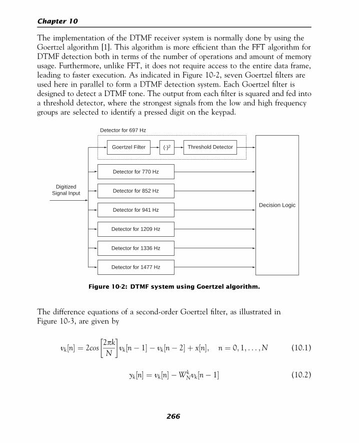
The implementation of the DTMF receiver system is normally done by using theGoertzel algorithm [1]. This algorithm is more efficient than the FFT algorithm forDTMF detection both in terms of the number of operations and amount of memoryusage. Furthermore, unlike FFT, it does not require access to the entire data frame,leading to faster execution. As indicated in Figure 10-2, seven Goertzel filters areused here in parallel to form a DTMF detection system. Each Goertzel filter isdesigned to detect a DTMF tone. The output from each filter is squared and fed intoa threshold detector, where the strongest signals from the low and high frequencygroups are selected to identify a pressed digit on the keypad.
The difference equations of a second-order Goertzel filter, as illustrated inFigure 10-3, are given by
vk½n� ¼ 2cos2pkN
� �vk½n� 1� � vk½n� 2� þ x½n�; n ¼ 0; 1; . . . ;N (10.1)
yk½n� ¼ vk½n� �WkNvk½n� 1� (10.2)
DigitizedSignal Input
Detector for 697 Hz
Goertzel Filter (.)2 Threshold Detector
Detector for 770 Hz
Detector for 852 Hz
Detector for 941 Hz
Detector for 1209 Hz
Detector for 1336 Hz
Detector for 1477 Hz
Decision Logic
Figure 10-2: DTMF system using Goertzel algorithm.
266
Chapter 10

where x n½ � denotes input, yk n½ � denotes output, vk n½ � denotes intermediate output,
the subscript k indicates frequency bin, N is the DFT size, and WkN ¼ exp �j
2pkN
� �.
The initial conditions are assumed to be zero, i.e., vk �1½ � ¼ vk �2½ � ¼ 0. Consideringthat only the magnitude of the signal is required for the DTMF tone detection,the following equation is used to generate magnitude squared outputs:
yk N½ �j j2 ¼ v2k N½ � þ v2k N� 1½ � � 2cos2pkN
� �vk N½ �vk N� 1½ � (10.3)
The coefficients 2cos2pkN
� �are selected based on the DTMF tones. They are listed
in Table 10-1.
Table 10-1: Fundamental Frequencies
Fundamental Frequency (Hz) Coefficient
697 1.703275
770 1.635585
852 1.562297
941 1.482867
1209 1.163138
1336 1.008835
1477 0.790074
x [n]
2cos2πκN
vk[n]
yk[n]
–WNk
–1
Σ Σ
Z–1
Z–1
Figure 10-3: Structure of a second-order Goertzel filter.
267
DSP System Design: Dual Tone Multi-Frequency (DTMF) Signaling

10.1 Bibliography
[1] E. Ifeachor and B. Jervis, Digital Signal Processing: A Practical Approach,Prentice-Hall, 2001.
268
Chapter 10

Lab 10: Hybrid Programming of DualTone Multi-Frequency System
In this lab, a DTMF system is built by using the LabVIEW hybrid programmingapproach.
L10.1 DTMF Tone Generator System
Before building a BD for the DTMF system, let us begin by creating a keypad, asshown in Figure L10-1. The 12 buttons shown are grouped into a cluster so that theiroutputs are wired via a cluster wire. This is done by placing a Cluster shell (Controls »Modern » Array, Matrix & Cluster » Cluster) on the FP and then by locating TextButtons (Controls » Express » Buttons & Switches » OK Button) in the cluster area.
Figure L10-1: Creating a cluster control.
269

The width and height of a button can be adjusted for having a larger display on theFP. This is achieved by choosing the buttons and then selecting the option Set Widthand Height from the Resize Objects menu of the FP toolbar, as shown in Figure L10-1.In this example, both the width and height of the buttons are set to 30. Also, themechanical action of the buttons is configured to be Latch When Released by right-clicking on the buttons and choosing Mechanical Action from the shortcut menu.Once the configuration of a button is complete, the button is copied multipletimes to construct a keypad. Change the Boolean text of the buttons appropriately.Align and distribute the buttons via Align Objects and Distribute Objects on theFP toolbar.
Next, the output value of the cluster control is specified for each button, i.e., thevalue coming out of the output of the cluster control when one of the buttons ispressed. To accomplish this, right-click on the border of the cluster and chooseReorder Controls In Cluster from the shortcut menu. This brings up the window shownin Figure L10-2. The numbers shown in the black background correspond to themodified order and the numbers in the white background to the original order.
Figure L10-2: Reordering cluster control.
270
Lab 10

The number assigned to a key is displayed next to Click to set to shown on thetoolbar. Click the buttons in a sequential order to specify the value shown in thetoolbar area. After finishing the assignment of the values to the buttons, click theOK button to finish reordering controls or the X button to cancel the changes.
Right-click on the border of the cluster and choose Auto Sizing » Size to Fit to resizethe cluster, if desired. Also, rename the label of the cluster as Keypad.
The BD of the built DTMF system is shown in Figure L10-3. Note that the keypadcluster control is shown as an icon on the BD. This VI generates a tone dependingon the number pressed on the keypad in the FP. The DTMF decoder based on theGoertzel algorithm can be seen in the lower half of the BD.
Figure L10-3: BD of the DTMF system.
271
Hybrid Programming of Dual Tone Multi-Frequency System

To build the BD, wire the output value of the cluster to an array by using theCluster to Array function (Functions » Programming » Cluster & Variant » Clusterto Array). This is done in order to have the value of each button as an element of anarray. The array is then wired to a Search 1D Array function to search for theTrue values among the array elements. In other words, this is done to check thestatus of the buttons considering that the index of the array, which is greater than orequal to zero, is returned when a button is pressed; otherwise, –1 is returned.
Thus, if the index of the array becomes greater than or equal to zero, i.e., any buttonis pressed, a DTMF signal is generated and the decoding part in the True case of theCase Structure is executed. In the False case of the Case Structure,a time delay is included to continue the idle status until a key is pressed.
Now, let us go through the DTMF signal generation for the True case of the CaseStructure. The value of the array index is wired to the Quotient &Remainder function with 3 as divisor. Since the numbers on the keypad arearranged in 3 columns and 4 rows, the remainder of this operation becomes thecolumn index, and the quotient becomes the row index. Based on the column androw indices, a high and a low tone value are chosen using two 1D array constants.The low and high tone values are wired to a Sine Waveform VI to generate awaveform based on the chosen frequencies.
The generated waveform is scaled to an 8-bit integer so that it can be played at anaudible volume level. An Expression Node (Functions » Programming » Numeric »Expression Node) is used for scaling the waveform. An Expression Node is usefulfor evaluating a simple equation or expression containing a single variable [1].A Play Waveform VI (Functions » Programming » Graphics & Sound » Sound »Output » Play Waveform) is located to send out the waveform to the PC sound card.This is an Express VI which plays data from the sound output device based on afinite number of samples. The Get Waveform Components and BuildWaveform VIs are used to build the waveform of the generated samples. For thespectral analysis of the generated samples, a Spectral Measurement Express VIand a waveform graph are used. The Spectral Measurement Express VI isconfigured as linear amplitude spectrum with no windowing.
At this stage, the DTMF generator is complete. The next section covers thedecoding module.
272
Lab 10

L10.2 DTMF Decoder System
The Goertzel algorithm is used for the decoding of DTMF signals. The BD shown inFigure L10-4 illustrates the Goertzel algorithm described by Equation (10.3) usinga MATLAB Script Node.
The inputs of this subVI consist of a 1D array of 205 samples and the coefficients ofthe Goertzel algorithm. A Text Ring control (Controls » Modern » Ring & Enum »Text Ring), labeled as Freq/Coeff, is located on the FP. Its data representationand properties are then modified as illustrated in Figure L10-5. This is done byright-clicking on the Text Ring in the FP and then choosing Edit Items. . . from theshortcut menu. Note that this Goertzel subVI is designed to incorporate onlythe first harmonic. It uses 205 input samples, and its coefficients are calculatedbased on 205 frequency bins.
The output of the Goertzel subVI is a Boolean value which indicates whether thespecified frequency component is present in the input samples. This is decided bycomparing the squared output of this subVI with a threshold value. The thresholdvalue here is empirically set to 5000.
In the BD of the DTMF system shown in Figure L10-3, a total of seven GoertzelsubVIs are placed to detect each frequency of a DTMF signal. The outputs of theGoertzel subVIs are grouped into two arrays to incorporate the row and column
Figure L10-4: BD of Goertzel algorithm.
273
Hybrid Programming of Dual Tone Multi-Frequency System

frequencies. From these arrays, indices of the True values are searched to determinea pressed key. A string constant gets referred to by the indices of the 2D array ofstring constants.
To create the 2D array of string constants, first place an Array Constant shell(Functions » Programming » Array » Array Constant) on the BD. Then, place a StringConstant (Functions » Programming » String » String Constant) in the ArrayConstant. As a result, a 1D array of string constants is created. In order to increasethe dimension of the array, right-click on the Array Constant and choose AddDimension from the shortcut menu. Now, enter the corresponding strings in the2D array.
Figure L10-5: Ring properties.
274
Lab 10

The output of the DTMF is shown in Figure L10-6. Notice that, when the button #is pressed, two frequencies are observed at 941 Hz and 1477 Hz in the decodedoutput. Furthermore, the decoded output matches the expected outcome.
L10.3 Bibliography
[1] National Instruments, LabVIEW User Manual, Part Number 320999E-01,2003.
Figure L10-6: FP of the DTMF system.
275
Hybrid Programming of Dual Tone Multi-Frequency System

This page intentionally left blank

CHAPTER11DSP System Design:
Software-Defined Radio
This chapter covers a software-defined radio system built by using the LabVIEWhybrid programming approach. A software-defined radio consists of a programmablecommunication system where functional changes can be made by merelyupdating software. For a detailed description of software-defined radio, the readeris referred to [1], [2].
4-QAM (Quadrature Amplitude Modulation) is chosen to be the modulationscheme of our software-defined radio system, noting that this modulation is widelyused for data transmission applications over bandpass channels such as FAX modem,high-speed cable, multi-tone wireless, and satellite systems [2]. For simplicity, herethe communication channel is considered to be ideal or noise-free.
11.1 QAM Transmitter
For transmission, pseudo noise (PN) sequences are generated to serve as our messagesignal. A PN sequence is generated with a five-stage linear feedback shift registerstructure, as shown in Figure 11-1, whose connection polynomial is given by
hðDÞ ¼ 1þ D2 þ D5 (11.1)
where D denotes delay and the summations represent modulo 2 additions.
The sequence generated by the preceding equation has a period of 31(¼ 25 � 1).Two PN sequence generators are used in order to create the message sequencesfor both the in-phase and quadrature phase components. The constellation of 4-QAMis shown in Figure 11-2. For more details of PN sequence generation, refer to [2].
277

Note that frame marker bits are inserted in front of the generated PN sequences.This is done for frame synchronization purposes, as discussed in the followingreceiver section. As illustrated in Figure 11-3, a total of 10 frame maker bits islocated in front of each period of a PN sequence.
Q
1
1 I
−1
−1
Figure 11-2: Constellation of 4-QAM.
1
0
FrameMarker Bits
FrameMarker Bits
PN Sequence (Length = 31)
Am
plitu
de
−1
Figure 11-3: PN sequence generator.
+
+ + + +
D D D D Dy(n−1)
h1 h2 h3 h4 h5
y(n−2) y(n−3) y(n−4) y(n−5)
y(n)
x(n)
Figure 11-1: PN generation with linear feedback shift register.
278
Chapter 11

The generated message sequences are then passed through a raised-cosine FIR filterto create a band-limited baseband signal. The frequency response of the raised cosinefilter is given by
GðfÞ ¼
1 for jf j � ð1� aÞfc
cos2p
4afc
�jf j � ð1� aÞfc
�" #for ð1� aÞfc� jf j � ð1þ aÞfc
0 elsewhere
8>>>><>>>>:
(11.2)
where a 2 ½0; 1� denotes a roll-off factor specifying the excess bandwidth beyond theNyquist frequency fc.
The output of the raised cosine filter is then used to build a complex envelope, ~sðtÞ,of a QAM signal expressed by
~sðtÞ ¼X1k¼�1
ck gTðt� kTÞ (11.3)
where ck indicates a complex message, made up of two real messages ak and bk,ck ¼ ak þ jbk.
When ~sðtÞ is modulated with ejoct, an analytical signal or pre-envelope, sþðtÞ, isgenerated,
sþðtÞ ¼ ~sðtÞejoct ¼X1k¼�1
ck gTðt� kTÞejoct (11.4)
The transmitted QAM signal, sðtÞ, is thus given by
sðtÞ ¼ Âe½sþðtÞ�¼ aðtÞcosðoctÞ � bðtÞsinðoctÞ
(11.5)
where Âe½�� corresponds to the real part of the complex value inside the brackets.
Figure 11-4 illustrates the block diagram of the QAM transmitter just discussed.Notice that the two data paths, indicated by a solid line and a dotted line,represent complex data. Again, the reader is referred to [2] for more theoreticaldetails.
279
DSP System Design: Software-Defined Radio

11.2 QAM Receiver
11.2.1 Ideal QAM Demodulation
Here, it is assumed that the exact phase and frequency information of the carrieris available. The received QAM signal is denoted by rðtÞ. To simplify thesystem, an ideal channel is assumed between the transmitter and the receiver,i.e., rðtÞ ¼ sðtÞ.If rðnTÞ is considered to be the sampled received signal, the analytic signal rþðnTÞ isgiven by
rþðnTÞ ¼ rðnTÞ þ jrðnTÞ (11.6)
where rð�Þ indicates the Hilbert transform of rð�Þ. Thus, the complex envelope of thereceived QAM signal ~rðnTÞ can be expressed as
~rðnTÞ ¼ rþðnTÞe� jocn T
¼ aðnTÞ þ jbðnTÞ (11.7)
Such a QAM demodulation process is illustrated in Figure 11-5.
HilbertTransform
g (nT )
g (nT )
g (nT ) = an + jbn
an�
e-xx
bn
g+ (nT )
ˆ
ˆ
Figure 11-5: Ideal demodulation [2].
PNGenerator
an
bn
cn = an + bn
PNGenerator
ImpulseModulator
c *(t )Pulse Shaping
Filter gT (t )
ejwc t
s (t ) S+(t) S(t )Re(.)
~
Figure 11-4: QAM transmitter [2].
280
Chapter 11

11.2.2 Frame Synchronization
Frame synchronization is required for properly grouping transmitted bits into analphabet. To achieve this synchronization, a similarity measure, consisting of cross-correlation, is computed between the known marker bits and received samples. Thecross-correlation of two complex values v and w is given by
Rwv½j� ¼X1n¼�1
�w½n�v½nþ j� (11.8)
where the bar denotes complex conjugate.
An example of the cross-correlation outcome for frame synchronization is shown inFigure 11-6. The maximum value is found to be at the location of index 33. Thesubsequent message symbols are then framed from this index point.
11.2.3 Decision-Based Carrier Tracking
Let us now consider the phase offset, denoted by y, between the transmitter and thereceiver. Based on this offset, the received signal can be written as
~rðnTÞ ¼ rþðnTÞe�jðocn TþyÞ
¼ cne�jy
(11.9)
where cn indicates the output of a slicer mapping a received sample to the nearestideal reference in the signal constellation. As a result, the baseband error at thereceiver is given by
~eðnTÞ ¼ cn �~rðnTÞ (11.10)
20
15
10
XC
orr
5
00 5 10 15 20 25
Index30 35 40 45 50
Figure 11-6: Cross-correlation of frame marker bits and received samples.
281
DSP System Design: Software-Defined Radio

Next, the LMS update method is used to minimize a decision-directed cost function,JDDðyÞ, consisting of the mean squared baseband error
JDDðyÞ ¼ avg j~eðnTÞj2h i
¼ avg ~eðnTÞe~ðnTÞh i (11.11)
By differentiating JDDðyÞ with respect to y, we get
dJDDðyÞdy
¼ avgd½~eðnTÞ~eðnTÞ�
dy
" #
¼ 2avg Âe ~eðnTÞ d~eðnTÞdy
( )" # (11.12)
where
d~eðnTÞdy
¼ d
dy½cn �~rðnTÞ� ¼ � d~rðnTÞ
dy(11.13)
and
d~rðnTÞdy
¼ �jcne�jy ¼ �j~rðnTÞ (11.14)
Equation (11.12) can thus be rewritten as
dJDDðyÞdy
¼ 2avg Âe ~eðnTÞj~rðnTÞn oh i
¼ �2avg Ám ~eðnTÞ~rðnTÞn oh i
¼ �2avg Ám cn~rðnTÞn oh i
(11.15)
where Ám½�� corresponds to the imaginary part of the complex value inside thebrackets.
282
Chapter 11

By writing the term Ám cn~rðnTÞ� �
in polar form, we get
Ám cn~rðnTÞ� � ¼ Ám Rcejbc Rre
jbrn o
¼ RcRr sinðbr � bcÞ(11.16)
Thus,
sinðbr � bcÞ ¼Ám cn~rðnTÞ
� �RcRr
(11.17)
Note that for small br � bc,
sin ðbr � bcÞ � br � bc
Rr�Rc ¼ jcnj(11.18)
As a result, the phase error DyðnÞ is given by
DyðnÞ ¼Ám ~eðnTÞ~rðnTÞ
n ojcnj2
(11.19)
Figure 11-7 shows a block diagram of the preceding tracking equations.
When both phase and frequency tracking are considered, the carrier phase of thereceiver becomes
fðnþ 1Þ ¼ fðnÞ þ DfðnÞ (11.20)
Slicercn
ℑm(.)
x (nT)
z−1
� k1
k2
�
+
+
+y (n)
Δq(n) Δj (n)
e(nT )
(.)
|.|21
y (n − 1)
Figure 11-7: Decision-directed carrier phase and frequency tracking.
283
DSP System Design: Software-Defined Radio

In this case, the phase update DfðnÞ is given by
DfðnÞ ¼ k1DyðnÞ þ cðnÞ (11.21)
where cðnÞ denotes the contribution of frequency tracking, which is expressed as
cðnÞ ¼ cðn� 1Þ þ k2DyðnÞ (11.22)
The scale factors k1 and k2 are configured to be small here, and usually k1=k2 � 100is required for phase convergence [2].
11.3 Bibliography
[1] C. Johnson and W. Sethares, Telecommunication Breakdown: Concepts ofCommunication Transmitted via Software-Defined Radio, Prentice-Hall, 2004.
[2] S. Tretter, Communication System Design Using DSP Algorithms, KlumerAcademic/Plenum Publishers, 2003.
284
Chapter 11

Lab 11: Hybrid Programmingof a 4-QAM Modem System
The design of a 4-QAM modem system is covered in this lab. As shown inFigure L11-1, this system consists of the following functional modules: messagesource, pulse shape filter, QAM modulator, Hilbert transformer, QAM demodulator,frame synchronizer, and phase and frequency tracker. The system is divided into twoparts: transmitter and receiver. The first three modules (message source, pulse shapefilter, and QAM modulator) make up the transmitter side; and the other modules,the receiver side. The building of each functional module is described in the sectionsthat follow.
Figure L11-1: System-level VI of 4-QAM modem.
285

L11.1 QAM Transmitter
The first component of the QAM modem is the message source. Here, PN sequencesare used for this purpose. Frame marker bits are inserted in front of these sequences toachieve frame synchronization. The BD of the Message Source VI is shown inFigure L11-2.
The generated samples are oversampled four times. This is done by comparing with 0the remainder of the global counter, indicated by n, divided by 4. Thus, out offour executions of this VI, one message sample (frame marker bit or PN sample) isgenerated. For the remaining three executions of the VI, zero samples are generated.The total length of the message for one period of a PN sequence and frame markerbits is 164, which is obtained by 4 (oversampling rate) � [10 (frame marker bits) þ31 (period of PN sequence)]. A constant array of 10 complex numbers is used tospecify the marker bits. Note that the real parts of the complex values are used as theframe marker bits of the in-phase samples and the imaginary parts as the framemarker bits of the quadrature-phase samples. In order to create complex constants,
Figure L11-2: Message Source VI.
286
Lab 11

one needs to change the representation of a numeric constant by right-clicking on itand choosing Representation » Complex Double (or Complex Single).
The BD of the PN Generator VI is shown in Figure L11-3. With this subVI, apseudo noise sequence of length 31 is generated by XORing the values of the secondand fifth shift registers.
The Shift Register, Select,and MathScript Node VIs are used tocompute a new PN sample. A For Loop with one iteration and a First Call?function (Functions » Programming » Synchronization » First Call?) are used to pass theshift register value of a current call to a next call of the subVI. The FirstCall? function checks whether a current call is occurring for the first time. If that isthe case, the shift register values are initialized by their specified initialvalues. Otherwise, the old values of the shift registers are passed from the previousexecution of the subVI. Notice that the PN Generator VI shown in Figure L11-3is built with the consideration of porting the algorithm to a DSP hardware platform.Alternatively, the built-in Binary MLS VI (Functions » Signal Processing » SignalGeneration » Binary MLS) can be used for the LabVIEW implementation.
Figure L11-3: PN Generator VI.
287
Hybrid Programming of a 4-QAM Modem System

Next, the generated samples are passed to a pulse shape filter shown in Figure L11-4.A raised cosine filter is used to serve as the pulse shape filter. The FIR FilterPtByPt VI is utilized for this purpose. The two outputs of the pulse shape filters arecombined to construct the pulse-shaped message signal by using the Re/Im toComplex function (Functions » Programming » Numeric » Complex » Re/Im toComplex).
As for the filter coefficients, they can be designed by a filter design tool, such as theone discussed in Lab 4, and stored in an array of constants.
The signal passed through the pulse shape filter is then connected to the QAMmodulator shown in Figure L11-5. The QAM modulated signal sðtÞ is obtained bytaking the real part of the pre-envelope signal sþðtÞ. This is achieved by performinga complex multiplication between the complex input and a complex carrierconsisting of a cosine and a sine waveform. This completes the modules of thetransmitter. In the next section, the modules of the receiver are built.
Figure L11-4: Pulse shape filter.
288
Lab 11

L11.2 QAM Receiver
The first module on the receiver side is the Hilbert transformer. This module buildsthe required analytic signal for demodulation based on the transmitted QAM signal.
A Hilbert transformer is built by using the DFD Remez Design VI (Functions »Addons » Digital Filter Design » Filter Design » Advance FIR Filter Design » DFD RemezDesign) of the DFD toolkit. To have an integer group delay, an even number, such as32, is specified as the filter order. The DFD Filter Analysis Express VI iswired to analyze the group delay of the filter as well as its magnitude and phaseresponse, as shown in Figure L11-6.
The specifications of the Hilbert transformer are similar to those of a bandpass filter,as indicated in Figure L11-7. Notice that only one element of the cluster array isneeded to design the Hilbert transformer. However, when a control is created at theband specs terminal of the DFD Remez Design VI, there are two default clustervalues. The second element, indexed at 1, should thus be deleted. To do this, selectthe element of the cluster array to be deleted; then right-click and choose DataOperation » Delete Element from the shortcut menu.
By running the VI, one can see the magnitude, phase response, and group delay ofthe Hilbert transformer, as shown in Figure L11-7.
Figure L11-5: QAM modulator.
289
Hybrid Programming of a 4-QAM Modem System

The array of indicators corresponding to the Hilbert transform coefficients is con-verted to an array of constants to be used by the other VIs. Note that the design andanalysis of the Hilbert transformer are needed only in the designing phase, not in theimplementation phase of the modem system.
The BD of the Hilbert transformer using the coefficients obtained from the DFDtoolkit is shown in Figure L11-8.
A Data Queue PtByPt VI (Functions » Signal Processing » Point By Point » OtherFunctions PtByPt » Data Queue PtByPt) is employed in order to synchronize the inputand output of the Hilbert transformer. In other words, the input samples are delayeduntil the corresponding output samples become available. This is needed due tothe group delay associated with the filtering operation. For an FIR filter of 33 taps,the group delay is 16. An array of numeric constants corresponding to the filtercoefficients is set up based on the text file generated by a filter design tool. Here, anFIR filter has been used for the implementation of the Hilbert transformer insteadof the built-in VI of LabVIEW. This is done to allow its execution by a DSPplatform.
Figure L11-6: Building the Hilbert transformer.
290
Lab 11

Figure L11-7: Analysis of the Hilbert transformer.
Figure L11-8: Hilbert Transform VI.
291
Hybrid Programming of a 4-QAM Modem System

The analytic signal achieved from theHilbert transformer is demodulated by theQAMdemodulator, as illustrated in Figure L11-9. The demodulation process is similar tothe modulation process illustrated in Figure L11-5 except for the negative frequencypart.
Next, the QAM demodulated signal is decimated by 4. To do this, one can usea Case Structure so that every fourth sample is selected for processing, as illu-strated in Figure L11-1. The decimated signal is sent to the Sync & TrackingVI for frame synchronization and phase/frequency tracking. The Sync &Tracking VI is an intermediate-level subVI incorporating several subVIs/functionsand operating in two different modes: frame synchronization and phase/frequency
Figure L11-9: QAM demodulator.
292
Lab 11

tracking. Let us examine the BD of this VI displayed in Figure L11-10. The inputsamples are passed into the receiver queue, implemented via the Complex QueuePtByPt VI (Functions » Signal Processing » Point By Point » Other Functions PtByPt »Complex Queue PtByPt), in order to obtain the beginning of a frame by cross-correlatingthe frame marker bits and received samples in the queue. The queue continues to befilled until it is completely full. Extra iterations are done to avoid including anytransient samples due to the delays associated with the filtering operations in thetransmitter.
The length of the queue is configured to be 51 in order to include the entire markerbits in the queue. This length is decided based on this calculation: 31 (one period ofPN sequence) þ 2 � 10 (frame marker bits). Also, 16 extra samples are taken toflush out any possible transient output of the filter, as mentioned previously. Bear inmind that the length of the queue or the number of extra reads varies based on thespecification of the transmitted signal, such as the length of the frame marker bitsand the number of taps of the phase shape filter. A counter, denoted by the LoopCount VI in Figure L11-11, is used to count the number of samples filling thequeue. Once the queue is completely filled and extra reads are done, the framesynchronization module is initiated.
Figure L11-10: Sync & Tracking VI—frame synchronization mode.
293
Hybrid Programming of a 4-QAM Modem System

The subVI for frame synchronization implemented within a MathScript Node isshown in Figure L11-12. In this subVI, the cross-correlation of the frame marker bitsand the samples in the receiver queue are computed. Lines 1 to 4 perform the
Figure L11-11: Loop Count VI.
Figure L11-12: Frame Synchronization VI.
294
Lab 11

complex cross-correlation operation as indicated in Equation (11.8). The absolutevalue of the complex correlation output is used to obtain the cross-correlation peak,since the location of this peak coincides with the beginning of the frame. The findfunction in line 5 is used to detect the index corresponding to the maximumcross-correlation value.
Once the index of the maximum cross-correlation value is obtained, all the datasamples are taken at this location of the queue. Consequently, the data bits getsynchronized.
The initial phase estimation is achieved using the phase of the complex data atthe beginning of the marker bits. Considering that the ideal reference is knownfor the first bit of the frame marker, 1þi in our case, this allows us to obtain thephase difference between the ideal reference and the received frame marker bits.The real and imaginary parts of data at the beginning of the marker bits are alsopassed to the Phase & Frequency Tracking VI to provide the initialconstellation.
The subVI of the frame synchronization is now complete. Locate the subVI on theBD of the Sync & Tracking VI shown in Figure L11-10. Notice that threelocal variables are created in order to pass the indicator values to the other partsof the VI which cannot be wired. In the Sync & Tracking VI, a RoundedLED indicator, labeled as Sync, is placed on the FP. A local variable is created byright-clicking either on the terminal icon in the BD or on the Rounded LEDindicator in the FP and choosing Create » Local Variable. Next, a local variableicon is placed on the BD. More details on using local and global variables can befound in [1].
The local variable Sync is used to control the flow of data for the frame synchro-nization. The initial value of the local variable is set to True to execute the framesynchronization. Then, it is changed to False within the Case Structure sothat it is not invoked again. The other two local variables, Initial Const andDelay Index, are used as the inputs of the phase and frequency tracking module,as shown in Figure L11-13.
295
Hybrid Programming of a 4-QAM Modem System

Now, let us describe the Phase & Frequency Tracking VI illustrated inFigure L11-14. A Formula Node (Functions » Programming » Structures »Formula Node) is shown in the upper part of the BD, which acts as a slicer todetermine the nearest ideal reference based on the quadrant on the I-Q plane.A Formula Node structure is capable of evaluating a script written in text-basedC code. There are numerous built-in mathematical functions and variables whichcan be used in a Formula Node. For example, pi represents p in the formulanode script shown in Figure 11-21. Further details on Formula Node can befound in [1].
The phase error, as shown in the BD in Figure L11-14, is computed from Equation(11.19). This error is multiplied by a small-scale factor to determine the phaseupdate D’ðnÞ in a second Formula Node implementing Equation (11.20).
Figure L11-13: Sync & Tracking VI—phase and frequency tracking mode.
296
Lab 11

Now, all the components of the modem system are completed. As the final step,a waveform chart and an XY Graph (Controls » Modern » Graph » XY Graph) areadded to the system-level BD shown in Figure L11-1. Figure L11-15 shows the FPof the system. After the phase is updated, the received signal becomes nearly aperfect reproduction of the transmitted signal except for the time delay. If thereexist a phase and a frequency offset with no tracking, the received signal appearsas shown in Figure L11-16. As displayed in this figure, the constellation of thereceived signal is rotated, and the amplitudes of some of the received samplesbecome too small. Obviously, the received signal will change by introducingchannel noise.
Figure L11-14: Phase & Frequency Tracking VI.
297
Hybrid Programming of a 4-QAM Modem System

The change in the constellation via the phase and frequency tracking is illustrated inFigure L11-17. The constellation of the samples in the I-Q plane becomes that ofthe ideal reference as the tracking operation progresses.
In summary, a 4-QAM transmitter and receiver system is built in LabVIEWby adopting a hierarchical approach. A simplified version of the systemhierarchy, displayed by choosing View » VI Hierarchy, is shown in
Figure L11-15: Initial phase estimation.
298
Lab 11

Figure L11-18. When the phase and frequency tracking module is used, thephase and/or frequency offset between the transmitter and receiver is successfullycompensated.
Note that all the subVIs discussed in this lab can be saved in a LabVIEW Library(LLB) file, e.g., Lab 11.llb. A new LLB file can be created by choosing New VI Libraryand naming it from the Name the VI window, which is brought up during the saveoperation.
Figure L11-16: Received signal with no phase and frequency tracking.
299
Hybrid Programming of a 4-QAM Modem System

Figure L11-18: Hierarchy of the QAM Modem VI.
Figure L11-17: Phase and frequencytracking in the I-Q plane.
300
Lab 11

L11.3 Bibliography
[1] National Instruments, LabVIEW User Manual, Part Number 320999E-01,2003.
301
Hybrid Programming of a 4-QAM Modem System

This page intentionally left blank

CHAPTER12DSP System Design: Cochlear
Implant Simulator
This chapter covers the real-time implementation of a cochlear implant signalprocessing simulator by using the LabVIEW hybrid programming approach.A cochlear implant is a prosthetic device surgically implanted into the innerear that is used to restore partial hearing in profoundly deaf people or patientssuffering from nerve deafness. In this device, sounds acquired from a microphoneare converted into electrical signals, which are then transmitted to a numberof implanted electrodes in the cochlea via radio waves leading to hearingperception [1]. This chapter covers the signal processing components of a cochlearimplant system and their implementations in a hybrid mode.
12.1 Cochlear Implant System
A cochlear implant system consists of the following four major components:(1) a microphone that picks up an input speech signal, (2) a signal processor thatconverts this signal into electrical signals, (3) a transmission system that transmitsthe electrical signals to implanted electrodes in the cochlea, and (4) an array ofelectrodes that are surgically inserted into the cochlea. Via the array of electrodes,auditory nerve fibers at different locations in the cochlea get stimulated dependingon the signal frequency. A signal processor is used for bandpass filtering the inputspeech signal into several (12–22) frequency bands. The processor converts thesignals from each band into electrical signals and delivers them to the array ofelectrodes. For a detailed description of cochlear implants, see [1].
Different signal processing strategies have been presented in the literature for con-verting acoustic signals to electrical signals [1], [2]. Here, a vocoder-based strategyknown as Continuous Interleaved Sampling (CIS) [2] is considered. This vocoder
303

strategy is widely used in commercial cochlear implants. In order to conduct aqualitative analysis of electrical stimuli obtained via the vocoder strategy, a synthesisstage is included along with the decomposition stage in our implementation, asillustrated in Figure 12-1. The synthesis method implemented here is based on thenoise-band vocoder simulation reported in [2].
As shown in Figure 12-1, during the decomposition stage, an input speech signal isfirst pre-emphasized and passed through a bank of bandpass filters. The cut-offfrequencies for the bandpass filters are obtained by logarithmically dividing thespeech signal bandwidth equally over a given number of channels. The envelopes ofthe filtered signals are then extracted via full-wave rectification and lowpass filteringwith a typical cut-off frequency of 400 Hz. During the synthesis stage, theenvelopes obtained after the decomposition are excited with white noise and thenfiltered through the same bank of bandpass filters that are used during thedecomposition stage. Finally, a synthesized signal is reconstructed by summing all thefiltered signals as indicated in Figure 12-1. In essence, the CIS strategy consists ofthe following signal processing parts: pre-emphasis filter, filterbank of bandpassfilters for decomposition and synthesis stages, envelope detection (full-waverectification þ lowpass filtering), and white noise excitation.
InputSignal Pre-
emphasis
BPF 2
BPF n
BPF 1
BPF 2
BPF n
BPF 1
Rectifier
Rectifier
Rectifier
LPF
LPF
LPF
DECOMPOSITION STAGE SYNTHESIS STAGE
BandpassFiltersEnvelope Detection
BandpassFilters
Excitationwith White
Noise
SynthesizedSpeechSignal
Figure 12-1: Noise-band vocoder simulation of cochlear implants.
304
Chapter 12

12.2 Real-Time Implementation
In order to process acquired speech frames from a microphone in real-time, thecoefficients of the filters need to be computed. The real-time implementation of theCIS strategy is done here in two phases: Design and Real-Time [3]. In the Designphase, the filter coefficients for the pre-emphasis filter, bandpass filters, and lowpassfilter are computed based on user-specified characteristics including filter orderand cut-off frequency. In addition, a white noise sequence is generated for noiseexcitation during the synthesis stage depending on the frame length specified bythe user. In the Real-Time phase, all the computed filter coefficients together withthe white noise sequence are fed back continuously within a real-time loop, asindicated in Figure 12-2.
In the real-time loop, an input frame is first acquired from a microphone at a givensampling rate. The pre-emphasized output is then passed through the filter bankdecomposition and synthesis stages. Finally, the synthesized frames are sent toa speaker or headphone to provide audio feedback. This process is repeatedcontinuously within the real-time loop until the user halts the process. Since thisprocess is based on continuous acquisition and processing of input frames, havinga real-time throughput is essential. For this purpose, it is required to completethe processing of a current frame before a next frame is captured. In other words,the total processing time for a frame should not exceed its length in time. Moredetails of each of the CIS components follow.
FilterbankDecomposition
(Analysis)
Read CurrentFrame From
Microphone InputDesign
CurrentFrame
Filter Coefficients
Envelopes FilterbankSynthesis
SynthesizedFrame Speakers or
Headphones
White Noise
Real-Time Loop(Repeated until stopped by user)
Figure 12-2: Real-time implementation flow of noise-band vocoder strategy.
305
DSP System Design: Cochlear Implant Simulator

12.2.1 Pre-Emphasis Filter
The pre-emphasis component consists of a first order IIR filter whose forwardcoefficients bp and reverse coefficients ap are given by
bp ¼ 1� exp �1200 � 2 � pi=Fsð Þ½ �ap ¼ 1� exp �3000 � 2 � pi=Fsð Þ½ �
(12.1)
where Fs denotes the sampling frequency.
12.2.2 Filterbank for Decomposition and Synthesis
During the decomposition stage, the bandpass filter associated with each channelpasses only a certain frequency band ½ f1ðiÞ f2 ðiÞ� of the entire input speech signalbandwidth ½ flow fhigh �, where f1ðiÞ and f2ðiÞ denote the lower and upper cut-off fre-quencies for the ith bandpass filter, and flow and fhigh the lowest and highest fre-quencies of the speech signal. The frequency band of a channel ½ f1ðiÞ f2 ðiÞ� isdetermined by logarithmically dividing the entire signal bandwidth equally inton channels. In other words, the upper and lower cut-off frequencies for the ithchannel bandpass filter are specified as
f1ðiÞ ¼ flow � 10Cb�ði�1Þ
Fs
!(12.2)
f2ðiÞ ¼ flow � 10Cb�ðiÞ
Fs
!(12.3)
where Cb denotes the channel bandwidth given by
Cb ¼log10ðfhigh=flowÞ
n
� �(12.4)
12.2.3 Envelope Detection
The full-wave rectified output of each channel is obtained by taking the absolutevalue of the corresponding bandpass filter output. This output is then passed througha lowpass filter having a cut-off frequency normally set at 400 Hz to extract itsenvelope.
306
Chapter 12

12.2.4 White Noise Excitation
Finally, a white noise sequence is used to modulate the envelope of each channel.Here, a white noise sequence is generated by passing a uniformly distributedpseudorandom sequence with the values in the range [–1 1] through the sgn functiondefined as
sgnðxÞ ¼�1; x< 00; x¼01; x>0
0@ (12.5)
307
DSP System Design: Cochlear Implant Simulator

12.3 Bibliography
[1] P. Loizou, “Mimicking the human ear,” IEEE Signal Processing Magazine,vol. 15, pp. 101–130, 1998.
[2] P. Loizou, “Speech processing in vocoder-centric cochlear implants,”Cochlear and Brainstem Implants (ed. Moller, A.), Adv. Otorhinolaryngol.Basel, Karger, vol. 64, pp. 109–143, 2006.
[3] V. Peddigari, N. Kehtarnavaz, and P. Loizou, “Real-time LabVIEWimplementation of cochlear implant signal processing on PDA platforms,”Proceedings of IEEE Conference on Acoustics, Speech and Signal Processing,vol. 2, pp. 357–360, 2007.
308
Chapter 12

Lab 12: Hybrid Programming ofCochlear Implant Simulator System
This lab shows how a cochlear implant simulator can be built in a hybrid mode as aDSP system design application example. Figure L12-1 illustrates the system-levelBD of such a system consisting of the following functional modules: filter designand real-time loop. The filter design module is executed only once before thereal-time loop is initiated for the purpose of computing the pre-emphasis, bandpass,and lowpass filter coefficients depending on user-specified input parameters.Then, the processing is repeated continuously in a While Loop until the userhalts the program by choosing the Exit control. It uses two Case Structures:one to initiate the real-time loop via a Start Boolean control and the otherto stop the real-time loop via a Stop Boolean control. For each of theseBoolean controls, first right-click and choose the Properties menu. Under theProperties menu, choose the Operation tab and set the Button behavior asLatch when released.
When the user presses the Start Boolean control, the DesignFilterCoeff VIcomputes the pre-emphasis, bandpass, and lowpass filter coefficients and passes themto a C DLL. The C DLL implements the system within a real-time loop using theCALLBACK function supported by Windows APIs [1]. Once the real-time loop isinitiated via CALLBACK, the cochlear implant signal processing keeps running inthe background till halted via the Stop Boolean control or the Exit control.When the Stop Boolean control is pressed, the real-time loop is halted, and thememory allocated to all global variables gets cleared.
As can be seen from Figure L12-1, a Flat Sequence Structure (Functions »Programming » Structures » Flat Sequence Structure) is used to initialize theProcessing Time (ms) before initiating the cochlear implant simulator.The Processing Time (ms) indicates the amount of time which is requiredto obtain a synthesized frame for an input speech signal frame. More details onbuilding the functional module DesignFilterCoeff subVI and the C DLLincorporating the functions StartCISProcess and StopCISProcess arepresented next.
309

L12.1 Filter Design
The cochlear implant simulator presented here is built using the vocoder-basedContinuous Interleaved Sampling (CIS) strategy. Figure L12-2 shows the BD ofthe DesignFilterCoeff VI, which computes the pre-emphasis filter, bandpassfilter, and lowpass filter coefficients, along with the white noise sequence. As shown
Figure L12-1: System-level VI of Cochlear Implant Simulator.
310
Lab 12

in this figure, an Expression Node (Functions » Mathematics » Numeric » ExpressionNode) is used to compute the pre-emphasis filter coefficients given by Equation(12.1). The sampling frequency, Srate, is passed as an input to the ExpressionNode to evaluate the first-order pre-emphasis filter coefficients, which include bothforward and reverse coefficients PreEmpFor and PreEmpRev, respectively.
Next, a white noise sequence, named White Noise, is generated using theUniform White Noise VI (Functions » Signal Processing » Signal Generation »
Figure L12-2: Filter Design VI.
311
Hybrid Programming of Cochlear Implant Simulator System

Uniform White Noise). The length of the white noise sequence is equal to the numberof samples in the acquired speech frame and is specified by passing the FrameLength to the Uniform White Noise VI. Then the output of the UniformWhite Noise VI, which generates uniformly distributed pseudo random numbersin the range [–1 1], is passed through the Sign VI (Functions » Programming »Numeric » Sign) to obtain the white noise sequence according to Equation (12.5). Itshould be noted that this white noise sequence is used to modulate the envelopesobtained during the decomposition stage of CIS as discussed earlier. The followingsubsections elaborate more on the design of lowpass and bandpass filter coefficients.
L12.1.1 Bandpass Filter Design
As a first step toward the design of the bandpass filters, it is required to compute thecut-off frequencies of each channel. Figure L12-3 shows the system-level BDof the ComputeCutoff VI to compute the cut-off frequencies according to
Figure L12-3: Compute Cut-off Frequencies VI.
312
Lab 12

user-specified input parameters. The inputs UpperFreq and LowFreq to this VIcorrespond to the input speech signal bandwidth as specified by flow and fhigh and thenChannels denotes the number of channels n. First, this VI computes the channelbandwidth or interval Cb by using the Logarithm Base 10 VI (Functions » Mathe-matics » Elementary & Special Functions » Exponential Functions » Logarithm Base 10). Thecomputed channel bandwidth Cb is then passed to a For Loop (Functions » Pro-gramming » Structures » For Loop) along with the sampling frequency Srate Fs forcomputing the cut-off frequencies of the ith channel according to Equations (12.2)and (12.3). To evaluate the cut-off frequencies of the ith channel, one needs to usebasic arithmetic VIs together with the Power Of 10 VI (Functions » Mathematics »Elementary & Special Functions » Exponential Functions » Power Of 10). The arrays UC andLC indicate the upper and lower cut-off frequencies for each of the n channels.
After the cut-off frequencies are computed, they are passed to the BPFDesignVI to compute the bandpass filter coefficients of each channel that are used bothin the decomposition and synthesis stages. Figure L12-4 shows the BD of theBPFDesign VI.
As indicated in Figure L12-4, a For Loop structure is used to compute the bandpassfilter coefficients of each channel. The UpperCutOff and LowerCutOfffrequencies obtained from the ComputeCutoff VI along with the BandpassFilter Type and Bandpass Filter Order are passed to the For Loopstructure. A Case Structure is used to support these three different types of IIRfilter design: Butterworth, Elliptic, and Chebyshev. These filters are part ofAdvanced Filter Design (Functions » Addons » Digital Filter Design » Filter Design »
Figure L12-4: Bandpass Filter Design VI.
313
Hybrid Programming of Cochlear Implant Simulator System

Advanced Filter Design) in the Digital Filter Design toolkit [2]. To achieve this, oneneeds to use an Enum (Controls » Modern » Ring & Enum » Enum) control forBandpass Filter Type corresponding to these three different filter types.The VIs for IIR filter design that are part of the Digital Filter Design toolkit areutilized here. Once the filter coefficients are obtained in the IIR filter cluster, theforward and reverse coefficients bpforwCoeffSGL and bprevCoeffSGL ofeach channel are extracted using the Unbundle By Name VI (Functions »Programming » Cluster & Variant » Unbundle By Name). Since the filter design using theDigital Filter Design toolkit generates the IIR filter cluster in terms of SecondOrder Sections (SOS), the BPFDesign VI also computes the number of SOS,bpSections, for any given channel. It should be noted that the UpperCutOffand LowerCutOff frequencies are normalized cut-off frequencies, and theBandpass Filter Order is thus doubled before passing it to the IIR filter designVIs as per the specifications of the filter design VIs.
L12.1.2 Lowpass Filter Design
The lowpass filter is used for extracting envelopes of each channel during thedecomposition stage. Figure L12-5 shows the BD of the LPFDesign VI to computethe lowpass filter coefficients based on user-specified input parameters: FilterType, LP Filter Order, Cutoff Frequency, and Sampling Frequency.Similar to the bandpass filter design, a Case structure is used to support thesethree different types of IIR filter design: Butterworth, Elliptic, and Chebyshev.To achieve this, one can use an Enum control for Filter Type corresponding tothese filter types. The VIs for IIR filter design that are part of the Digital FilterDesign toolkit are utilized here. Once the filter coefficients are obtained in the IIR
Figure L12-5: Lowpass Filter Design VI.
314
Lab 12

filter cluster, the forward and reverse coefficients lpforwCoeffSGL and lprev-CoeffSGL are extracted using the Unbundle By Name cluster. Since the filterdesign using the Digital Filter Design toolkit generates the IIR filter cluster in termsof Second Order Sections (SOS), the LPFDesign VI also computes the number ofSOS, lpSections, for the designed lowpass filter.
The outputs of the LPFDesign VI and BPFDesign VI form part of the outputs ofthe DesignFilterCoeff VI. These outputs, along with the other outputs,namely the pre-emphasis filter coefficients and white noise sequence, are passed to aC DLL, which implements the real-time module. Further details on building the CDLL and its various functions are provided in the following section.
L12.2 Real-Time Implementation
The real-time implementation of the CIS strategy is carried out in a hybrid modeusing the Call Library Function Node (Functions » Connectivity » Libraries &Executables » Call Library Function Node) feature of LabVIEW. This function allowsone to invoke C codes via Dynamic Link Library (DLL) and helps to reduce theprocessing time [3]. Before invoking the functions within a C code, one needs tocreate a Dynamic Link Library. To create a DLL, use the Visual Studio IDE appli-cation. Create a New » Project under File menu and select Win32 Project under theVisual C++ Project type. Enter the Project name as CIS, choose the option Createdirectory for solution, and enter the Solution name to be the same as Project name,i.e., CIS. Now, set the Application Settings as Dynamic Link Library and choose an EmptyProject. After creating the Win32 Dynamic Link Library Project solution with thepreviously mentioned steps, add the source file CIS.cpp and the header file CIS.h tothe project. Before building the project, make sure that the path of the header fileis added to Additional Include Directories under Project » Properties » ConfigurationProperties » C/C++ » General. Remember that the header file should be included forboth the Release and Debug configurations of the project. Next, choose the Build »Batch Build menu and check to build both the Release and Debug configurations.Once the build is complete, it should create DLLs for both the Release and Debugconfigurations in the respective directories under the Project. The CIS.dllcorresponding to the Release configuration is used to configure the Call LibraryFunction Node by selecting the appropriate exported function.
Both the source and header files are included in the accompanying CD under thefolder LabVIEW Labs\Lab12. In order to avoid the overhead associated withcalling the C DLL each time a new speech frame is acquired by using the LabVIEWsound acquisition VIs, the supplied source file CIS.cpp utilizes Windows APIs toacquire speech frames from a microphone. It then processes acquired frames based on
315
Hybrid Programming of Cochlear Implant Simulator System

the noise-band vocoder strategy to obtain synthesized frames and play them backcontinuously to a speaker using Windows APIs. This is achieved by utilizing theCALLBACK function supported by Windows APIs. Two buffers are used for acqui-sition and playback so that while one buffer is used for acquiring current samples, theother buffer is used for processing samples.
The source file CIS.cpp has a number of functions that perform different tasks. Thesetasks are summarized in Table L12-1. It should be noted that among all these func-tions, only the two functions StartCISProcess and StopCISProcess areexported to the C DLL and get invoked using the Call Library FunctionNode feature of LabVIEW. All the other functions are local to the C code and areinvoked internally. Also, it is important to note that the C code for the bandpassand lowpass filtering is generated based on the pseudo code obtained from the FixedPoint tools of the Digital Filter Design toolkit, as indicated in Figure L12-6.
Table L12-1: Building Functions
S.No. Function Name Tasks Performed
1. StartCISProcess Initializes all filter coefficients and other parametersto global variables and then sets up the CIS real-time loop using CALLBACK function supported byWindows APIs.
2. StopCISProcess Stops the real-time loop using the CALLBACKfunction and then clears all memory allocated toglobal variables.
3. InitializeSound Initializes sound input and output device, that ismicrophones and speakers. It sets up buffers forspeech frames acquisition and playback ofsynthesized speech. Also, it enables theCALLBACK function to invoke the real-time loop.
4. CreateMixBuffer Creates output buffers to write synthesized framesthat need to be played back to speakers.
5. CreateInMixBuffer Creates input buffers to acquire speech frames from amicrophone for further processing according to theCIS strategy and obtains synthesized frames.
6. WaveInCallbackFunction CALLBACK function invokes the functionProcessAudioBuffer whenever a new speech frame isacquired and ready to be processed.
7. ProcessAudioBuffer Processes an acquired input speech frame accordingto the CIS strategy, which includes both thedecomposition and synthesis stages and finallyobtains synthesized speech for playback ontospeakers.
316
Lab 12

Table L12-1: Building Functions—Cont’d
S.No. Function Name Tasks Performed
8. DestroySound Closes input and output devices that were openedusing Windows APIs. It also clears all memoryallocated for global variables.
9. PreEmphasis Performs the pre-emphasis filtering to obtain pre-emphasized output.
10. FullWaveRect Obtains the full-wave rectified output of an inputsignal.
11. BandpassFilteringFP Initializes the previous states of each second ordersection of the designed bandpass filter for a givenchannel and then invokes the functionBPFilter_FilteringFP to filter each inputsample of current speech frame.
12. BPFilter_FilteringFP Obtains a corresponding bandpass filter output for agiven input sample by passing through a cascadedstages of second order sections.
13. LowpassFilteringFP Initializes the previous states of each second ordersection of the designed lowpass filter for a givenchannel and then invokes the functionLPFilter_FilteringFP to filter each inputsample of current speech frame.
14. LPFilter_FilteringFP Obtains the corresponding lowpass filter output for agiven input sample by passing through a cascadedstages of second order sections.
Figure L12-6: Generate C code using Fixed-Point tools of DFD toolkit.
317
Hybrid Programming of Cochlear Implant Simulator System

As indicated in Figure L12-6, the designed floating-point filter coefficients are firstquantized to generate a fixed-point filter using DFD FXP Quantize Coef(Functions » Addons » Digital Filter Design » Fixed-Point Tools » DFD FXP Quantize Coef),and then DFD FXP C Code Generator (Functions » Addons » Digital FilterDesign » Fixed-Point Tools » DFD FXP Code Generator) is used to generate the C code.When the VI is executed, it creates the pseudo code for fixed-point filtering in Cand stores the files in the specified path. One can locate the source file created andmodify the fixed-point filtering code in C to floating-point filtering accordingly—that is, by changing the input and output data types and removing the scale factors.It should be noted that the C code thus generated implements the filteringoperation using cascaded stages of second order sections.
Once the DLL is created, the functions are exported via the Call LibraryFunction Node feature in LabVIEW, as shown in Figure L12-1. As indicated inthis figure, one of the Call Library Function Nodes is configured to invokethe exported function StartCISProcess, whereas the other is configured to
Figure L12-7: Interactive FP of cochlear implant simulator.
318
Lab 12

invoke the exported function StopCISPro-cess. In order to configure any Call LibraryFunction Node, right-click on the CallLibrary Function Node and choose theConfigure option. Then choose the path of the CDLL, select the exported function, and add theappropriate input and output parameters as perthe definition of the exported function.
As can be seen from Figure L12-1, all the relevantinputs are passed to the C DLL via the CallLibrary Function Node. When the userpresses the Stop Boolean control, the synthesizedframe last obtained and the Processingtime(ms) are displayed; see the simulator FPdisplayed in Figure L12-7. It should be realizedthat the pointers to the output variables are passedto the C DLL, and then the output is updatedwithin the C DLL accordingly. The FP of thesimulator allows the user to interactively changevarious input parameters and then observe thecorresponding change in outputs. When the userpresses the Start Boolean control, the synthe-sized frame is played back to the speakers inresponse to the speech through a microphone andhalts the program either when the Stop Booleancontrol or the Exit control is pressed.
In summary, a cochlear implant simulator systemis built in hybrid mode. A simplified version ofthe system hierarchy, displayed by choosing View » VI Hierarchy, is shown inFigure L12-8. When C DLLs are used, the real-time implementation of the CISstrategy, which includes the decomposition and synthesis stages, is achieved. Allthe subVIs discussed in this lab can be saved in a LabVIEW Library (LLB) file, e.g.,Lab 12.llb. A new LLB file can be created by choosing New VI Library and naming itfrom the Name the VI window, which is brought up during the save operation.
Figure L12-8: Hierarchy ofcochlear implant simulator VI.
319
Hybrid Programming of Cochlear Implant Simulator System

L12.3 Bibliography
[1] Microsoft Developer Network, Visual Cþþ, MSDN Library VisualStudio, 2007.
[2] National Instruments, Digital Filter Design Toolkit (search keywords),http://www.ni.com.
[3] National Instruments, Integrating C DLLs (search keywords), http://www.ni.com.
320
Lab 12

Index
Aacoustic signals, 303adaptive filtering systems
DSP integration of, 248system identification of, 248–251
adaptive FIR filter, usages of, 157A/D converter, 62
bitstream of, 84characteristic of, 63data quantization effect, 127quantization effect, analog signal, 80
output signal, 82–84quantization error, 81–83
quantization noise, 63additive quantization noise, 63Add Zeros VI, 88aliasing, of discrete time signal, 60analog signal
processing of, 1sampling of, 57
analog-to-digital signal conversionquantization, 63–64sampling, 57signal reconstruction, sinewave, 65–66Sine Wave VIs for
aliased signal, 72inputs to, 71
application programming interfaces(APIs), 229
arraycreation using auto-indexing, 33–34of data elements, 16
Array Subset function, 116auto-indexing, 33
input array, For Loop, 86
BBandpass filters, 304, 306Bandpass IIR filter. See IIR filterbandwidth, 279baseband signal, 279Basic Function Generator VI, 46binary bitstream, 86binary point, 124
Block Diagram (BD)of aliasing, 72–73building
Express VI and function, 11–12structure, graphical enclosure, 13–14terminal icon, 12wires, data transfer, 12–13
control and indicator icons, 30of Express VI FFTs, 76of FFT and STFT, 187of noise cancellation system, 168of signal generation and amplification
system, 38of signal reconstruction system, 88Subtract function on, 163of system identification, 164wiring of, 24
boolean control, 309breakpoints, 16, 205, 216–218, 220–221Building C DLL, 51–52Build Options of CCS, 236Butterworth Filter VI, 248Butterworth IIR filter, 121
CCALLBACK function, 316Calling C DLL, 52–54Call Library Functionbuilding C DLL, 51–52calling C DLL, 52–54configuration of, 54
Call Library Function Node VI, 119cascade coefficient cluster, 111–112cascaded filter, stages of, 96Cascaded integrator comb (CIC), 98cascade-form coefficients, 112case selector, 14Case Structure, 14CCS Automation, 231CCS Build VI, 226CCS Communication VIs, 235CCS Download Code VI, 226CCS Open Project VI, 226CCS Reset VI, 226
CCS RTDX Read, 234CCS RTDX Read Array SGL VI, 235CCS RTDX Write Array SGL, 234CCS RTDX Write VI, 234CCS Run VI, 226C DLL, 309central processing unit (CPU), 197C function, process for adding, 218channel noise, 297Chebyshev IIR filter, 121Chebyshev method, 94Chirp Pattern VI, 186CIC. See Cascaded integrator combCIS.cpp, 315–316C Langauge, filtering code written in, 233cluster control, 269clusters, 16cochlear implant simulator vi, hierarchy
of, 319cochlear implant system
components of, 303filter design
bandpass filter design, 312–314DesignFilterCoeff VI, 310–312lowpass filter design, 314–315
interactive FP of, 318noise-band vocoder simulation of, 304system-level VI of, 310
Code Composer Studio (CCS), 204–205,207, 223
automation process for, 226,231–233
RTDX communication, 227code execution, time profiling using
breakpoints for, 221coefficient quantization, 128compiler options, 212Compiling, 205Composite Signal VI, 186conditional terminal, 14configuration dialog box, 77connector pane, of LMS VI, 163Continuous Interleaved Sampling (CIS)
real-time implementation of, 305
321

call library function node,configuration, 315
decomposition and synthesis,filterbank for, 306
pre-emphasis filter, 306white noise excitation, 307
Control palettes, 9Controls, 9Convolution VI, 90count terminal, 13Create Histogram Express VI, 83–84C6x DSK Target Boards
configuration and peripherals of, 201memory organization of, 202–203
Ddata transmission applications, 277Data type conversion, 134Data type mismatch, 133Data Types, 130debugging tools, for removing errors on
DSP programs, 214decision-directed carrier phase, 283decomposition tree, 193designed floating-point filter
coefficients, 318DesignFilterCoeff VI, 309–310DFD. See Digital Filter DesignDFD Build Filter from Cascaded Coef
VI, 112DFD Build Filter from TF VI, 112, 147DFD Classical Filter Design Express
VI, 97, 99, 103–104, 107, 238DFD Convert Structure VI, 150DFD filter analysis, 289DFD Filter Analysis Express VI, 99, 107DFD Filtering VI, input and output signal
of, 104DFD FXP Coef Report VI, 145DFD FXP Quantize Coef VI, 143DFD FXP Simulation VI, 144DFD Get Cascaded Coef VI, 107DFD Pole-Zero Placement Express VI, 97DFD Remez Design VI, 289DFT. See Discrete Fourier transformdifference equation, 93Digital Filter Design (DFD), 93
fixed-point and analysis of, 98methods, comparison of, 97multi-rate, 98
Digital Filter Design toolkit, 97–98, 314,316–317
digital filtering and filtersdifference equations of, 93–95FIR filter, 233–238fixed-point format of, 143–146IIR filter, 238–243stability and structure of, 95–97
digital frequency, 57Digital signal processing
advantages of, 1courses, 2growth and development in, 1
digital signal processor (DSP)components of signal processing system
on, 197configuration of, 227–230debugging tools for, 214design, 265with Express VI
autoscaled graph of, 43–44FP of, 45Multiply function, 42–43resizing, 41–42signal generation, 37Simulate Signal, 38–39, 43Time Delay, 40waveform graph, 38, 44
fixed-point implementation of, 133implementation, 197integration
BD of filtering system with, 234of noise cancellation system, 252system identification with, 248
programming methods for, 203compiling process, 205–206linking, 205using software tools: Code Composer
Studio, 204–205with regular VIs, creation
Basic Function Generator VI, 46–47BD and FP of, 48cluster constant, 46waveform graph, 47While Loop, 46
digitization process, 1direct-form coefficients, 112direct memory access (DMA), 198Discrete Fourier transform, 60
computational complexity of, 62for periodic discrete signals, 61
discrete time signalaliasing problem, 60Fourier transform of, 59generation of, 69sampling, 57
discrete wavelet transform(DWT), 175–176, 178–180
advantages of, 190–194DLL. See Dynamic Link LibraryDSK Target Boards, 201DSP FIR Filtering System VI, 238DSP hardware platform, 287DSP programming, 203DSP Starter Kit (DSK) board, 201DSP systems. See Digital signal processor
(DSP)DSP Test Integration for TI DSP, 223DSP Test Integration Palette, 227DTMF decoder system, 273
DTMF receiver systemimplementation of, 266tone detection for, 267
DTMF tone generator system, 269–272dual tone multi-frequency (DTMF)
signaling, 265hybrid programming of, 269
Dynamic Link Library (DLL), 115Visual Studio IDE application, 315
Eelectrical signals, 303Elliptic Bandpass Filter, 107Equi-ripple method, 93, 99error term, of FIR filter, 158–159Example Finder, 225Expression Node, 72Express VI, 99appearances of, 11–12block diagram object, 11periodicity of DFT, 76Time Delay, 33–34vs. regular VIs, 37–49
External Memory Interface (EMIF), 198
FFast Fourier transform (FFT)of discrete signals, 61–62of N-point signal, 175–176of sinusoids, 62, 78–79
Feedback Node, 163–165FFT. See Fast Fourier transformFFT algorithmDSP integration of, 254for DTMF detection, 266
FFT and STFT transformations, differenceof, 183–189
property node, 189–190FFT PtByPt VI, 115Filter design VI, 311Finite Impulse Response (FIR), 93finite word length, 127–128FIR. See Finite Impulse ResponseFIR filteranalysis of, 101design of, 101, 113–115DFD toolkit and design of, 99–101frequency response of, 279implementation of
calling DLL, 119–120DLL creation and C, 118–119point-by-point processing, 115–118
PtByPt VI, 288, 293specifications, 113VI of, 101–105
FIR Filter PtByPt VI, 115, 162FIR lowpass filter, 233for achieving fixed-point filtering on
DSP, 244configuration of, 100
322
Index

C source code for, 237source code of fixed-point version
of, 245–247FIR transfer function, 148fixed-point
digital filtering, 143filter coefficient, 144implementation
and arithmetic operations onDSP, 244
vs. floating point, 123processor, 123tools VIs, 98
floating-pointimplementations of, 123number representation, 128–129
For Loop structure, 13auto-indexing for, 33–34
Formula Waveform VI, 81, 85Forward Coefficients, 112Fourier series, for periodic analog
signals, 61Fourier transform
of analog signal, 59of continuous-time signal and its
discrete time version, 59of digital signal, 59
FP. See Front panelFractional representation, 124frame synchronization
cross-correlation of, 281MathScript node, subVI for,
294–295Sync & tracking VI, 293
frequency domain transformationsdiscrete wavelet transform,
178–180fast Fourier transform and discrete
wavelet transform, 175–176short-time Fourier transform,
176–178signal processing toolset, 180
frequency offset, 297frequency tracking, 283, 298Front Panel (FP)
buildingalign, distribute, and resize objects
menu for, 10–11control options for, 9indicator options for, 10
configuration of, 21graphical code on, 22numeric control, 25of reconstructed sinewave, 87
full-wave rectification, 304
GGoertzel algorithm, 271, 273Goertzel filters, 266graphical programming, 2Graph palette, 78–79
HHanning window VI, 189Heisenberg’s uncertainty principle, 183Hilbert transform, 280histogram, of quantization error, 64, 81–83Horizontal pointer slide controls and
signal frequency, 101–104Host Port Interface (HPI), 198hybrid programming, 50, 269, 285
IIcon Editor, 27IDWT. See Inverse DWTIIR. See Infinite Impulse ResponseIIR bandpass filter, configuration of, 106IIR Chebyshev bandpass floating-point
filter, 154IIR elliptic bandpass floating-point
filter, 154IIR filter, 128, 130, 150, 238–243, 248BD of, 110design, 106–110design methods, responses of, 95difference equation of, 93–94filtering system, 110–111FP of, 111stability and structure of, 96transfer function of, 96, 109vs. FIR filter, 96
IIR Filter Cluster, 107IIR Filtering Design.vi, 107–108Impulse Pattern VI, 186Impulse Response (IIR) filter, 93Index Array function, 168Indicators palette, 10Infinite Impulse Response (IIR), 93Initialize Array VI, 166–167input/output transfer function, of A/D
converter, 63–64integrated development environment
(IDE). See Code ComposerStudio (CCS)
inverse Chebyshev method, 94Inverse DWT (IDWT), 180inverse system identification, 173iteration terminal, 13–14, 31, 33
JJoint Test Action Group (JTAG), 223Joint Time-Frequency Analysis
(JTFA), 180
Kkeypad, 265Knob Properties dialog box, 29
LLabeling tool, 21, 44Laboratory Virtual Instrumentation
Engineering Workbench.See LabVIEW
LabVIEWcall library function feature
building C DLL, 51–52calling C DLL, 52–54
communication C6x DSK board, 223configuration and integration process
for, 226–227data types in, 130–132Digital Filter Design toolkit, 97–98,
314, 316–317DSP test integration toolkit for TI
DSP, 223–224graphical environment, 2
controls palette and tools palette, 8functions palette, 7
handling data types in, 133–135hybrid programming, 265
summation and averagingoperations, 50–51
installation of, 3–4MathScript Interactive Window,
14–16MathScript node feature of, 141steps required for
implementing, 224–225, 249virtual instruments (VIs) of
creation of, 20–32front panel (FP) and block diagram
(BD), 5–6icon and connector pane, 6
LabVIEW Digital Filter Design toolkitfilter design of, 97fixed-point and analysis of, 98multi-rate, 98
LabVIEW hybrid programming, 303LabVIEW library (LLB) file, 319LabVIEW sound acquisition VIs, 315Least mean square algorithm (LMS), BD
of, 161least significant bit (LSB), 64linker command file, for creation of
executable file, 210LMS update method, 282LMS VI
connector pane of, 163graphical representation of, 162
Logic analyzer BD, 86Loop count VI, 293–294Lowpass filtering, 304
MMathScript
analog and discrete signalgeneration, 69–70
characteristics of, 121inputs and outputs of, 14, 16Interactive Window, 14interfaces, 14–15
MathScript Node, 161–162MathScript Node VIs, 287MATLAB Script Node, 162, 273
323
Index

mean squared baseband error, 282Memory organization, 202Merge Signals function
automatic insertion of, 38inputs, 39
modulation, 277Multi-channel Buffered Serial Port
(McBSP), 198multi-channel serial communication
link, 198Multiply function, 42Multirate Filter Design VIs, 98
Nnoise-band vocoder simulation
of cochlear implants, 304real-time implementation of, 305
noise cancellation system, 158–159BD of, 161DSP integration of, 252FP of, 171
noise-cancelled output signal, 252noise corrupted signal, 158, 168noise source signal, 158, 168Numeric Constant, 22Numeric Indicators, 100Nyquist frequency, 279Nyquist rate, 60Nyquist theorem, 65
OOptional FIR filter specifications, 113Overflow handling, 135–137
Q-format conversion, 137–138
Pphase and frequency tracking module
in I-Q plane, 300received signal, 299Sync & Tracking VI, 296
phase error, 283phase estimation, 298Phase & frequency tracking VI,
296–297phase offset, 281pipelined CPU, 198–199PN generation, 277
with linear feedback shift register, 278point-by-point processing,
115–118polymorphic VI, 138
creation of, 138–140probe points, 215Probe tool, 16, 35–36Profile tool, 16–17, 54property node, in FFT and STFT
graphs, 189–190Pseudo code
bandpass and lowpass filtering, 316for fixed-point filtering, 318
pseudo noise (PN), 277sequence, 287
pulse shape filter, 288
QQAM demodulator signal, 292QAM modem
system-level VI of, 285VI, hierarchy of, 300
QAM modulator, 288–289QAM receiver
decision-based carriertracking, 281–284
frame synchronization, 281Hilbert transformer, 289–290
analysis of, 291–292DFD Remez Design VI, 289
QAM demodulation, 280QAM transmitter, 277
block diagram of, 279–280message source VI of, 286
Q15 Conv VI, 139Q-format conversion, 137–138Q-format number, representation of, 123Quadrature amplitude modulation
(4-QAM), 277constellation of, 278
quantization, 63of analog signal, 64
using A/D converter, 80–83
Rrandom number, 33Real-Time Data Exchange (RTDXTM), 223
communication channel, 229communication speed for, 235procedure to avoid errors for, 235
real-time implementationof CIS strategy, 315of noise-band vocoder, 311–313
reconstruction kernel, 87Remez algorithm. See Equi-ripple methodReplace Array Subset, 162Reverse Coefficients, 112ring control, 185Rotate 1D Array, 162RTDX error, 235Run button, 22Run-time support library, 227
Ssampling
analog sinusoidal signal, 57frequency domain, signals, 60of 251 Hz signal, 79periodicity condition of, 61
Scaled Signals terminal, 38scaling, 130Scaling and Mapping Express VI
configuration of, 40
input signal amplification, 37Signals terminal of, 38
Scope chart mode, 163–164second-order filter, 240sgn function, 307shift registers, 163–165, 287Short-time Fourier transform
(STFT), 175–178STFT VI, 187
signal analysis interface, 216signal constellation, 281signal processing, in analog/digital
domain, 1Signal processing toolset (SPT), 180Signal processor, bandpass filtering, 303signal reconstructionof analog signal, 65–66Virtual Instruments (VI)
BD of, 88FP, reconstruction kernel, 87subVI of, 88–89
Simulate Signal Express VI, 38–39, 43, 76Simulation Report VI, 145Sinc functions, pulse approximation
of, 65–66Sinc Function subVI, 89Sine Waveform VI, 103, 135, 186sinewave generator, 207Sine Wave PtByPt VI, 115Software installation, 3Special Filter Design VIs, 97Spectral Measurements Express VI, 104Spectrogram, for STFT visualization, 177SPT. See Signal Processing Toolsetstability, 95standard Fourier transform, 176StartCISProcess, 309, 318stepwise horizontal interpolation
method, 86STFT. See Short-time Fourier transformStopCISProcess, 309, 319Strip chart mode, 163–164Structuresrepresentation of, 13–14uses of, 6
sum and average of two inputvalues, 29–31
SubVIAdd Zeros, 88–89creation of
connector pane pattern, 26icon editing, 27–28inputs and outputs of, 25
Sinc Function, 89use of
two input values, sum and averageof, 29–31
Super-Resolution Spectral Analysis(SRSA), 180
Sweep chart mode, 163–164
324
Index

Synchronous dynamic RAM(SDRAM), 201
system identification system, 157, 248BD of, 164LMS algorithm, 161–163shift register and feedback
node, 163–167waveform chart, 163
Ttelephone pad push buttons. See keypadterminal icons, 12textual programming, 14Time Delay Express VI, 33, 40Time-frequency resolutions, for
STFT, 178Time-frequency tiling, 179time-varying channel, of FIR
filter, 169–170TMS320C6x architecture, 197TMS320C6X DSP processor, 197–198
C64x DSP, 199–200pipelined CPU, 198–199
Tools palette, 8transfer function, assessment of, 96transfer function polynomials, 127Transform VI, 191, 193
UUniversal Serial Bus (USB) port, 223
VVery Long Instruction Word (VLIW)
architecture, 199Virtual Instrument (VI)block diagram
Express VI and function, 11–12structure, graphical enclosure,
13–14terminal icon, 12wires, data transfer, 12–13
creationblank, 20continuously running, 31–32horizontal/vertical space,
21–22numeric control, 25outputs, 21and save, 32SubVI, 25–29Wiring tool, 22
debugging and profiling ofProbe tool, 16, 35–36Profile tool, 16–17
front panel
align, distribute, and resize objectsmenu, 10–11
control options, 9Horizontal Pointer Slide control, 69indicator options, 10
icon and connector pane, 6for quantized discrete waveform
analysis, 84–85verification of, 32
vocoder strategy, 304
WWA Discrete Wavelet Transform VI, 193WA Inverse Discrete Wavelet Transform
VI, 191, 193Waveform Chart, 35, 116
updating modes in, 163–164Waveform decomposition tree, 193waveform graph, 44–45Waveform Graph Properties, 75Wavelet Transform VI, 191, 193WA Wavelet Filter VI, 190While Loop structure, 14white noise excitation, 307White noise VI, 311wires, 12–13Wiring tool, 22, 26, 31
325
Index